742 IEEE TRANSACTIONS ON COMPONENTS AND PACKAGING TECHNOLOGIES, VOL. 28, NO. 4, DECEMBER 2005
Printed Organic Transistors for Ultra-Low-CostRFID Applications
Vivek Subramanian, Member, IEEE, Paul C. Chang, Student Member, IEEE, Josephine B. Lee, Student Member, IEEE,Steven E. Molesa, and Steven K. Volkman
Abstract—Printed electronics provides a potential pathwaytoward the realization of ultra-low-cost radio frequency identi-fication (RFID) tags for item-level tracking of consumer goods.Here, we report on our progress in developing materials andprocesses for the realization of printed transistors for low-costRFID applications. Using inkjet printing of novel conductors,dielectrics, and organic semiconductors, we have realized printedtransistors with mobilities 10 1 cm2/V-s. AC performance ofthese devices is adequate for 135-kHz RFID, and, with furtheroptimization, 13.56-MHz RFID appears to be within reach. Wereview the performance of these devices, and discuss optimizationstrategies for achieving the ultimate performance goals requisitefor realizing ultra-low-cost printed RFID.
Index Terms—Organic semiconductors, printed electronics,radio frequency identification (RFID).
I. INTRODUCTION
I N RECENT years, there has been significant interest in thedevelopment of radio frequency identification (RFID) tags
for item-level tracking of individual consumer goods [1]. Suchtags are expected to dramatically improve automation, inven-tory control, and checkout/purchasing operations, provided theyare cheap enough to be widely deployed. For widespread de-ployment, a cost ceiling of 1–2 cents per tag has generally beenindicated by most consumer product companies. Printed elec-tronics is particularly promising for realizing such a low costceiling, since the cost of printed electronics is generally ex-pected to be two to three orders of magnitude cheaper than sil-icon per unit area. We briefly review the basic cost assumptionsdriving the development of printed RFID tags, explore the var-ious approaches being pursued, and describe our progress to-ward realizing the component technologies required to realizeultra-low-cost all-printed RFID.
Based on FCC regulations, RFID devices are generallybeing deployed in four main communication bands: 1) thelow-frequency range up to 135 kHz, 2) a band at 13.56 MHz,3) a band at 900 MHz, and 4) a band at 2.4 GHz [2]. Each bandhas its own advantages and disadvantages. The range of RFIDtags is typically larger at higher frequencies for reasons relatingto the antenna Q, and thus, most pallet-level RFID solutionsmake use of 900 MHz or 2.4 GHz [3]. Furthermore, since the
Manuscript received January 8, 2005; revised June 20, 2005. This work wasrecommended by Associate Editor J. E. Morris upon evaluation of the reviewers’comments.
The authors are with the Department of Electrical Engineering and ComputerSciences, University of California, Berkeley, CA 94720-1770 USA (e-mail:[email protected]).
Digital Object Identifier 10.1109/TCAPT.2005.859672
passive components (both inductors and capacitors) are smallerat these higher frequencies, total tag size can be reduced atthese frequencies, reducing cost.
For item-level tracking, unfortunately, these frequencies donot work particularly well due to the presence of substantialamounts of metal (for example, soup cans, etc), and RF-absorbing fluids (water, milk, etc.). Therefore, at this time,it appears that 13.56 MHz or lower is attractive from thisperspective, since absorption is substantially reduced at lowerfrequencies. In general, therefore, the sweet spot for item-levelRFID will likely exist at 13.56 MHz, though there is currentlya push for developing 900-MHz solutions as well. Tag size at135 kHz is generally too large, and likely too expensive forwidespread item level tracking use, and operational use of thehighest frequencies in metal-contaminated environments iscorrespondingly problematic.
II. CURRENT STATUS OF LOW-COST RFID DEVELOPMENT
Three main approaches are being pursued to realize ultra-low-cost RFID. In the conventional approach, low-cost siliconchips are used. The chip cost is miniscule, since typical tags(excluding the antenna) are less than 1 mm wide. Using variousattachment technologies such as pick-and-place [4] and fluidicself assembly [5]), the tags are added to a paper or plastic stripcontaining the external antenna. Unfortunately, costs for thisattachment operation do not appear to scale well at this time,and it seems unlikely that a silicon-based approach will realizesub-1-cent RFID in the foreseeable future. For cost reasons, sil-icon tags also generally operate in the higher frequency ranges,and are thus problematic in metal-contaminated environments,as discussed above.
A more aggressive approach is to make use of flexibleelectronics based on organic devices. Several groups are devel-oping such technologies [6]–[8]. Using vacuum sublimation,good performance has been achieved using organic materials,in particularly pentacene. Carrier mobilities 10 cm /V-shave been realized, with circuits operating at several MHz[7]. Unfortunately, all high-performance pentacene devicesto date make use of slow deposition processes that reducethroughput to unacceptable levels. Correspondingly, the use ofshadow-masking (required to achieve patterning) is economi-cally uncertain at this time. If progress is made toward realizinghigh-performance, high-throughput technologies based onvacuum-sublimation and shadow-masking, these vacuum-sub-limated organic thin film technologies (TFTs) may represent adisruptive path toward the realization of low-cost RFID.
SUBRAMANIAN et al.: PRINTED ORGANIC TRANSISTORS 743
Fig. 1. Process-flow used to fabricate printed transistors. Various p-type and n-type printable semiconductors have been developed.
The final approach being considered for the realization ofitem-level RFID is all-printed organic electronics [8], [9].In this process, an entirely additive printing process is usedto realize printed devices and circuits, thus eliminating theneed for lithography, vacuum processing, and subtractiveprocess steps. Printing is also potentially an extremely highthroughput technology. Thus, the costs associated with thistechnology are expected to be substantially lower than silicon-based techniques, particularly since the large area antenna iseasily integrated using this process. To date, performance ofprinted devices is generally lower than the aforementionedvacuum-based technologies, though progress has been rapidand sustained. Here, we will describe the results obtained in ourgroup that will hopefully allow performance to be improved tothe point where all-printed item-level RFID will be technicallyand economically feasible.
III. PRINTED TRANSISTORS: STATUS AND OUTLOOK
To realize item-level RFID, both high-quality printed passivecomponents (inductors and capacitors) and high-performance
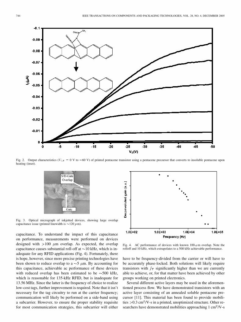
all-printed transistors are required. We have previously reportedon our printed passive component technologies [9]. Here, wewill focus on printed active components, specifically, transis-tors. To realize printed transistors, we use the general processflow shown in Fig. 1 [10]. A metallic gate line is printed, fol-lowed by a polymer dielectric. Next, source and drain contactsare printed, followed by a printed semiconductor. The net re-sult is the realization of a printed bottom-gate inverted staggeredtransistor structure. Using this structure, we typically obtain car-rier mobilities of approximately 10 cm /V-s (Fig. 2), withoutany optimization of contacts or interfaces. AC performance ofthese devices is, unfortunately, inadequate for 13.56-MHz RFIDapplications, though it is likely adequate for 135-kHz RFID.
Based on limitations of our inkjetting technology, it isdifficult to produce transistors with channel lengths less than10 m without substantial overlap capacitance. This is ap-parent by looking at an optical micrograph of a sample printeddevice (Fig. 3). Current limitations of inkjet-printing limitprinted gate length to 30 m or larger. To achieve the shortchannel length necessary for high-speed, the source and drainand substantially overlap over the gate, resulting in large
744 IEEE TRANSACTIONS ON COMPONENTS AND PACKAGING TECHNOLOGIES, VOL. 28, NO. 4, DECEMBER 2005
Fig. 2. Output characteristics (V = 0 V to �60 V) of printed pentacene transistor using a pentacene precursor that converts to insoluble pentacene uponheating (inset).
Fig. 3. Optical micrograph of inkjetted devices, showing large overlapcapacitance issue (printed linewidth is �120 �m).
capacitance. To understand the impact of this capacitanceon performance, measurements were performed on devicesdesigned with 100 m overlap. As expected, the overlapcapacitance causes substantial roll-off at 10 kHz, which is in-adequate for any RFID applications (Fig. 4). Fortunately, thereis hope, however, since more precise printing technologies havebeen shown to reduce overlap to a 5 m. By accounting forthis capacitance, achievable ac performance of these deviceswith reduced overlap has been estimated to be 500 kHz,which is reasonable for 135-kHz RFID, but is inadequate for13.56 MHz. Since the latter is the frequency of choice to realizelow-cost tags, further improvement is required. Note that it isn’tnecessary for the tag circuitry to run at the carrier frequency;communication will likely be performed on a side-band usinga subcarrier. However, to ensure the proper stability requisitefor most communication strategies, this subcarrier will either
Fig. 4. AC performance of devices with known 100-�m overlap. Note therolloff and 10 kHz, which extrapolates to a 500 kHz achievable performance.
have to be frequency-divided from the carrier or will have tobe accurately phase-locked. Both solutions will likely requiretransistors with significantly higher than we are currentlyable to achieve, or, for that matter have been achieved by othergroups working on printed electronics.
Several different active layers may be used in the aforemen-tioned process flow. We have demonstrated transistors with anactive layer consisting of an annealed soluble pentacene pre-cursor [11]. This material has been found to provide mobili-ties 0.3 cm /V-s in a printed, unoptimized structure. Other re-searchers have demonstrated mobilities approaching 1 cm /V-s
SUBRAMANIAN et al.: PRINTED ORGANIC TRANSISTORS 745
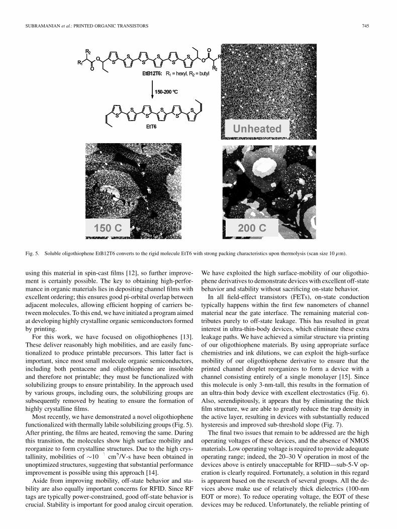
Fig. 5. Soluble oligothiophene EtB12T6 converts to the rigid molecule EtT6 with strong packing characteristics upon thermolysis (scan size 10 �m).
using this material in spin-cast films [12], so further improve-ment is certainly possible. The key to obtaining high-perfor-mance in organic materials lies in depositing channel films withexcellent ordering; this ensures good pi-orbital overlap betweenadjacent molecules, allowing efficient hopping of carriers be-tween molecules. To this end, we have initiated a program aimedat developing highly crystalline organic semiconductors formedby printing.
For this work, we have focused on oligothiophenes [13].These deliver reasonably high mobilities, and are easily func-tionalized to produce printable precursors. This latter fact isimportant, since most small molecule organic semiconductors,including both pentacene and oligothiophene are insolubleand therefore not printable; they must be functionalized withsolubilizing groups to ensure printability. In the approach usedby various groups, including ours, the solubilizing groups aresubsequently removed by heating to ensure the formation ofhighly crystalline films.
Most recently, we have demonstrated a novel oligothiophenefunctionalized with thermally labile solubilizing groups (Fig. 5).After printing, the films are heated, removing the same. Duringthis transition, the molecules show high surface mobility andreorganize to form crystalline structures. Due to the high crys-tallinity, mobilities of 10 cm /V-s have been obtained inunoptimized structures, suggesting that substantial performanceimprovement is possible using this approach [14].
Aside from improving mobility, off-state behavior and sta-bility are also equally important concerns for RFID. Since RFtags are typically power-constrained, good off-state behavior iscrucial. Stability is important for good analog circuit operation.
We have exploited the high surface-mobility of our oligothio-phene derivatives to demonstrate devices with excellent off-statebehavior and stability without sacrificing on-state behavior.
In all field-effect transistors (FETs), on-state conductiontypically happens within the first few nanometers of channelmaterial near the gate interface. The remaining material con-tributes purely to off-state leakage. This has resulted in greatinterest in ultra-thin-body devices, which eliminate these extraleakage paths. We have achieved a similar structure via printingof our oligothiophene materials. By using appropriate surfacechemistries and ink dilutions, we can exploit the high-surfacemobility of our oligothiophene derivative to ensure that theprinted channel droplet reorganizes to form a device with achannel consisting entirely of a single monolayer [15]. Sincethis molecule is only 3-nm-tall, this results in the formation ofan ultra-thin body device with excellent electrostatics (Fig. 6).Also, serendipitously, it appears that by eliminating the thickfilm structure, we are able to greatly reduce the trap density inthe active layer, resulting in devices with substantially reducedhysteresis and improved sub-threshold slope (Fig. 7).
The final two issues that remain to be addressed are the highoperating voltages of these devices, and the absence of NMOSmaterials. Low operating voltage is required to provide adequateoperating range; indeed, the 20–30 V operation in most of thedevices above is entirely unacceptable for RFID—sub-5-V op-eration is clearly required. Fortunately, a solution in this regardis apparent based on the research of several groups. All the de-vices above make use of relatively thick dielectrics (100-nmEOT or more). To reduce operating voltage, the EOT of thesedevices may be reduced. Unfortunately, the reliable printing of
746 IEEE TRANSACTIONS ON COMPONENTS AND PACKAGING TECHNOLOGIES, VOL. 28, NO. 4, DECEMBER 2005
Fig. 6. ID-VG characteristic for printed monolayer device (W/L = 250/3;VD = �35 V), showing excellent off-state characteristics due to near-idealelectrostatic configuration.
Fig. 7. Subthreshold characteristic of a monolayer device showing excellentsubthreshold slope <200 mV/dec, which is impressive considering the 100-nmEOT dielectric. In comparison, most printed devices have swings >1 V/dec.
thinner layers is difficult; however, alternative strategies thatlook promising have been demonstrated.
In a first strategy, a self-assembled monolayer has been usedto demonstrate 2-V operation and 100-mV/dec swing [16]. Thistechnique may be printing-compatible. In a second strategy,high-K dielectrics may be used [17]. We have demonstratedthe use of soluble high-K dielectric precursors to demonstratedevices with sub-4-V operation (Fig. 8) [9]. While substantialwork remains to be done to reduce low-field leakage, etc., thepromise of this technique is clear.
The dielectric is an important concern in all field-effectdevices, and relatively little effort has been dedicated to this inprinted electronics. Aside from the performance implicationsabove, recent results indicate that the dielectric interface alsocontributes to degraded stability; electrical stressing of printeddevices results in degradation of drive-current without a degra-dation of mobility (Fig. 9). This indicates that the primarydegradation mechanism is a threshold voltage shift, likelytaking place at/near the dielectric interface.
All the results above focus on p-channel metal-oxide semi-conductor (PMOS). The absence of an adequate n-type MOS(NMOS) material is a barrier to realization of complemen-tary MOS (CMOS), with its associated design simplicity and
Fig. 8. Output characteristics of a thiophene-based TFT with a high-kdielectric. The large low-leakage is evident, and is caused by the formation ofa porous, leaky TiO dielectric from the Ti-precursor (inset).
Fig. 9. Degradation characteristics of printed FETs showing mobility stabilityversus drive current degradation, measured in an inert environment. Thisdegradation is due to V instability.
low-power benefits. All organic NMOS materials to date havepoor performance ( 10 cm /V-s mobility) and stability[18]. Recently, we have demonstrated an alternate solutionto this problem. Using printed Zinc oxide nanoparticles, wehave demonstrated stable NMOS devices with mobilities of
0.1 cm /V-s [19]. While the results are early, they attest to thepotential of a hybrid approach to realizing printed electronics.
IV. CONCLUSION
Printed electronics provides a promising potential pathwaytoward the realization of ultra-low-cost RFID tags for item-level tracking of consumer goods. Using printing, we have re-alized printed transistors formed entirely using printed films in-cluding various novel organic semiconductors, dielectrics, andnanoparticle-based conductors. While the performance of thesedevices is currently inadequate for operation at the frequencyof choice, i.e., 13.56 MHz, improvement has been steady, andfurther improvements in knowledge along with the associatedtechnology optimization should ultimately enable the realiza-tion of all-printed RFID tags, ushering in an era of enhancedinventory efficiency and consumer convenience.
SUBRAMANIAN et al.: PRINTED ORGANIC TRANSISTORS 747
ACKNOWLEDGMENT
The authors would like to thank A. R. Murphy and J. M. J.Fréchet for assistance with synthesis of the oligothiophene ma-terials used herein.
REFERENCES
[1] R. Bansal, “Coming soon to a Wal-Mart near you,” IEEE AntennasPropag. Mag., vol. 45, no. 6, pp. 105–106, Jun. 2003.
[2] T. Scharfeld, “An analysis of the fundamental constraints on low-costpassive radio-frequency radio-frequency identification system design,”M.S. thesis, Mass. Inst. of Technol., Cambridge, MA, 2001.
[3] K. Finkenzeller, Ed., RFID Handbook : Fundamentals and Applica-tions in Contactless Smart Cards and Identification. New York: Wiley,2003.
[4] R. Imura, “The world’s smallest RFID mu-chip, bringing about newbusiness and lifestyles,” in VLSI Circuits Symp. Tech. Dig., 2004, pp.120–123.
[5] J. S. Smith, “High density, low parasitic direct integration by fluidic selfassembly (FSA),” in Int. Electron Devices Meeting Tech. Dig., 2000, pp.201–204.
[6] P. F. Baude, D. A. Ender, T. W. Kelley, M. A. Haase, D. V. Muyres, andS. D. Theiss, “Organic semiconductor RFID transponders,” in IEEE Int.Electronic Devices Meeting Tech. Dig., 2003, pp. 8.1.1–8.1.4.
[7] T. W. Kelley, D. V. Muyres, P. F. Baude, T. P. Smith, and T. D. Jones,“High performance organic thin film transistors,” in Proc. Materials Re-search Soc. Symp., vol. 771, 2003.
[8] A. Knobloch, A. Manuelli, A. Bernds, and W. Clemens, “Fully printedintegrated circuits from solution processable polymers,” J. Appl. Phys.,vol. 96, p. 2286, 2004.
[9] V. Subramanian, “Toward printed low-cost RFID tags: Device, materialsand circuit technologies,” presented at the 2nd Advanced TechnologyWorkshop on Printing an Intelligent Future: Printed Organic and Molec-ular Electronic Technologies, Boston, MA, Mar. 16–19, 2003.
[10] S. Molesa, M. Chew, D. Redinger, S. K Volkman, and V. Subramanian,“High-performance inkjet-printed pentacene transistors for ultra-low-cost RFID applications,” in Materials Research Soc. Spring Meeting,2004.
[11] S. Volkman, S. Molesa, B. Mattis, P. C. Chang, and V. Subramanian,“Inkjetted organic transistors using a novel pentacene precursor,” inProc. Materials Research Soc. Spring Meeting, Symp. H: FlexibleElectronics—Materials Device Technology, vol. 769, N. Fruehauf, B.R. Chalamala, B. E. Gnade, and J. Jang, Eds., 2003.
[12] A. Afzali, C. D. Dimitrakopoulos, and T. L. Breen, “High-performance,solution-processed organic thin-film transistors from a novel pentaceneprecursor,” J. Amer. Chem. Soc., vol. 123, pp. 8812–8813, 2002.
[13] A. R. Murphy, J. M. J. Frechet, P. C. Chang, J. B. Lee, and V. Sub-ramanian, “Organic thin film transistors from a soluble oligothiophenederivative containing thermally removable solubilizing groups,” J. Amer.Chem. Soc., vol. 126, p. 1596, 2004.
[14] P. C. Chang, J. Lee, D. Huang, V. Subramanian, A. R. Murphy, and J.M. J. Fréchet, “Film morhphology and thin film transistor performanceof solution-processed oligothiophenes,” Chem. Mater., to be published.
[15] P. C. Chang, S. E. Molesa, A. R. Murphy, J. M. J. Fréchet, and V. Subra-mamian, “Single-monolayer inkjetted oligothiophene OTFTS exhibitinglow leakage and high performance,” in Proc. IEEE Device ResearchConf., South Bend, IN, 2004, pp. 183–184.
[16] H. Klauk et al., “Molecular thin film transistors with a subthresholdswing of 100 mV/decade,” in IEDM’03 Tech. Dig., 2003, pp. 8.2.1–8.2.4.
[17] C. D. Dimitrakopoulos, S. Purushothaman, J. Kymissis, A. Callegari,and J. M. Shaw, “Low-voltage organic transistors on plastic comprisinghigh-dielectric constant gate insulators,” Science, vol. 283, p. 822, 1999.
[18] C. D. Dimitrakopoulos and D. J. Mascaro, “Organic thin-film transistors:A review of recent advances,” IBM Res. Dev., vol. 45, no. 1, pp. 11–27,2001.
[19] S. K. Volkman, S. E. Molesa, J. B. Lee, B. A. Mattis, A. de la FuenteVornbrock, T. Backhishev, and V. Subramanian, “A novel transparentair-stable printable n-type semiconductor technology using ZnOnanoparticles,” in Proc. IEEE Int. Electron Device Meeting, 2004, pp.769–772.
Vivek Subramanian (S’94–M’98) received theB.S. degree in electrical engineering from LouisianaState University, Alexandria, in 1994 and the M.S.and Ph.D. degrees in electrical engineering fromStanford University, Stanford, CA, in 1996 and1998, respectively.
He cofounded Matrix Semiconductor, Inc., in1998. Since 1998, he has been with the Universityof California, Berkeley, where he is currently anAssociate Professor in the Department of Electricalengineering and Computer Sciences. He has authored
more than 50 research publications and patents. His research interests includeCMOS devices and technology and polysilicon thin film transistor technologyfor displays and vertical integration applications. His current research focuseson organic electronics for display, low-cost logic, and sensing applications.
Dr. Subramanian was nominated to Technology Review’s list of top 100young innovators (the TR100), his work at Matrix Semiconductor was nom-inated to the Scientific American SA50 list for visionary technology, he wasnominated to the National Academy of Engineering’s “Frontiers of Engi-neering,” and received the National Science Foundation Young InvestigatorAward (CAREER) in 2003. He has served on the Technical Committee, DeviceResearch Conference and the International Electron Device Meeting.
Paul C. Chang (S’03) received the B.S. and M.S.degrees in electrical engineering from the Universityof California, Berkeley (UC Berkeley), in 2001 and2004, respectively. He is currently pursuing the Ph.D.degree in electrical engineering at UC Berkeley.
His recent research focuses on organic semicon-ductors.
Josephine B. Lee (S’03) received the B.S. degree inelectrical engineering and physics from the Univer-sity of Texas, Austin, in 2001 and is currently pur-suing the M.S. degree in electrical engineering at theUniversity of California, Berkeley.
She has interned with the Center for Non-linearDynamics, University of Texas, Austin, theMax-Plank Institute for Colloids and Interfaces, andthe National Institute of Child Health and HumanDevelopment. Her recent research focuses on organicsemiconductors.
Steven E. Molesa received the B.A. degree fromHope College, Holland, MI, in 2001 and the M.S.degree in electrical engineering from the Universityof California, Berkeley (UC Berkeley), in 2004.He is currently pursuing the Ph.D. degree at UCBerkeley.
Steven K. Volkman received the B.S. degree inchemical engineering from the University of Cali-fornia, Berkeley (UC Berkeley), in 2004.
He is currently a Research Staff Member in the Or-ganic Electronics Group, Electrical Engineering De-partment, UC Berkeley.


![IEEE Life Cycle Standards and the CMMI Implementation Considerations · 2017-05-19 · [IEEE 1998] IEEE 1062, IEEE Recommended Practice for Software Acquisition [IEEE 2005] IEEE 15288,](https://static.documents.pub/doc/80x56/5e740ab442e6042c3d2f498e/ieee-life-cycle-standards-and-the-cmmi-implementation-considerations-2017-05-19.jpg)


