215
ADVANCED AND EVER ADVANCING MITSUBISHI ELECTRIC MITSUBISHI 8-BIT SINGLE-CHIP MICROCOMPUTER 740 FAMILY / 740 SERIES 7531 Group User’s Manual MITSUBISHI ELECTRIC
ADVANCED AND EVER ADVANCINGMITSUBISHI ELECTRIC
MITSUBISHI 8-BIT SINGLE-CHIP MICROCOMPUTER740 FAMILY / 740 SERIES
7531Group
User’s Manual
MITSUBISHIELECTRIC
Keep safety first in your circuit designs!
Notes regarding these materials
Mitsubishi Electric Corporation puts the maximum effort into making semiconductorproducts better and more reliable, but there is always the possibility that trouble mayoccur with them. Trouble with semiconductors may lead to personal injury, fire orproperty damage. Remember to give due consideration to safety when making yourcircuit designs, with appropriate measures such as (i) placement of substitutive,auxiliary circuits, (ii) use of non-flammable material or (iii) prevention against anymalfunction or mishap.
These materials are intended as a reference to assist our customers in the selectionof the Mitsubishi semiconductor product best suited to the customer's application;they do not convey any license under any intellectual property rights, or any otherrights, belonging to Mitsubishi Electric Corporation or a third party.
Mitsubishi Electric Corporation assumes no responsibility for any damage, orinfringement of any third-party's rights, originating in the use of any product data,diagrams, charts, programs, algorithms, or circuit application examples contained inthese materials.
All information contained in these materials, including product data, diagrams, charts,programs and algorithms represents information on products at the time of publicationof these materials, and are subject to change by Mitsubishi Electric Corporationwithout notice due to product improvements or other reasons. It is thereforerecommended that customers contact Mitsubishi Electric Corporation or an authorizedMitsubishi Semiconductor product distributor for the latest product information beforepurchasing a product listed herein.The information described here may contain technical inaccuracies or typographicalerrors. Mitsubishi Electric Corporation assumes no responsibility for any damage,liability, or other loss rising from these inaccuracies or errors.Please also pay attention to information published by Mitsubishi Electric Corporationby various means, including the Mitsubishi Semiconductor home page (http://www.mitsubishichips.com).
When using any or all of the information contained in these materials, includingproduct data, diagrams, charts, programs, and algorithms, please be sure to evaluateall information as a total system before making a final decision on the applicability ofthe information and products. Mitsubishi Electric Corporation assumes noresponsibility for any damage, liability or other loss resulting from the informationcontained herein.
Mitsubishi Electric Corporation semiconductors are not designed or manufacturedfor use in a device or system that is used under circumstances in which human life ispotentially at stake. Please contact Mitsubishi Electric Corporation or an authorizedMitsubishi Semiconductor product distributor when considering the use of a productcontained herein for any specific purposes, such as apparatus or systems fortransportation, vehicular, medical, aerospace, nuclear, or undersea repeater use.
The prior written approval of Mitsubishi Electric Corporation is necessary to reprintor reproduce in whole or in part these materials.
If these products or technologies are subject to the Japanese export controlrestrictions, they must be exported under a license from the Japanese governmentand cannot be imported into a country other than the approved destination.Any diversion or reexport contrary to the export control laws and regulations of Japanand/or the country of destination is prohibited.
Please contact Mitsubishi Electric Corporation or an authorized Mitsubishi Semiconductor product distributor for further details on these materials or the products contained therein.
Rev. Rev.
No. date
1.0 First Edition 980801
2.0 The contents of revision are mainly as follows; 990924
• CHAPTER 1 HARDWARE
• 3.1 Electrical characteristics
• 3.2 Typical characteristics
• 3.6 Mask ROM confirmation form
• 3.7 Mark specification form
2.1 Updated as follows: 991109
•Page1-2; Power dissipation to 25 mW
•Page 1-14, Fig.13; Start address of Interrupt vector area to FFEC16
•Pages 3-6, 3-14, 3-22; Parameter to Linearity error from former Absolute accuracy
REVISION DESCRIPTION LIST 7531 GROUP USER’S MANUAL
(1/1)
Revision Description

Preface
This user’s manual describes Mitsubishi’s CMOS 8-bit microcomputers 7531 Group.After reading this manual, the user should have athrough knowledge of the functions and features ofthe 7531 Group, and should be able to fully utilizethe product. The manual starts with specificationsand ends with application examples.
For details of software, refer to the “740 FAMILYSOFTWARE MANUAL.”For details of development support tools, refer to the“Mitsubishi Microcomputer Development Support Tools”Hompage (http://www.tool-spt.mesc.co.jp/index_e.htm).
BEFORE USING THIS MANUAL
This user’s manual consists of the following three chapters. Refer to the chapter appropriate to your conditions,such as hardware design or software development. Chapter 3 also includes necessary information forsystems development. You must refer to that chapter.
1. Organization
CHAPTER 1 HARDWAREThis chapter describes features of the microcomputer and operation of each peripheral function.
CHAPTER 2 APPLICATIONThis chapter describes usage and application examples of peripheral functions, based mainly onsetting examples of relevant registers.
CHAPTER 3 APPENDIXThis chapter includes necessary information for systems development using the microcomputer, suchas the electrical characteristics, the list of registers, the Mask ROM confirmation form (for mask ROMversion), the ROM programming confirmation form (for One Time PROM version), and the Markspecification form which are to be submitted when ordering.
2. Structure of register
The figure of each register structure describes its functions, contents at reset, and attributes as follows :
Note 2: Bit attributes......... The attributes of control register bits are classified into 3 bytes : read-only, write-only and read and write. In the figure, these attributes are represented as follows :
: Bit in which nothing is arranged
0 1 :
Name Function At reset R WB
0
1
2
3
4
0
0
0
0
0
5
6
7
1
b0b1b2b3b4b5b6b7 Contents immediately after reset release
Bit attributes
(Note 1)
Processor mode bits
Stack page selection bit
Nothing arranged for these bits. These are write disabled bits. When these bits are read out, the contents are “0.”
Fix this bit to “0.”
Main clock (XIN-XOUT) stop bit
Internal system clock selection bit
0 0 : Single-chip mode
1 0 :1 1 :
Not available
b1 b0
0 : 0 page1 : 1 page
0 : Operating1 : Stopped0 : XIN-XOUT selected 1 : XCIN-XCOUT selected
: Bit that is not used for control of the corresponding function
0
Note 1:. Contents immediately after reset release0....... “0” at reset release1....... “1” at reset release?....... Undefined at reset release.......Contents determined by option at reset release
R.......Read ...... Read enabled.......Read disabled
W......Write ..... Write enabled...... Write disabled.......“0” write
(Note 2)
CPU mode register (CPUM) [Address : 3B 16]
Bits
7531 Group User’s Manual i
Table of contents
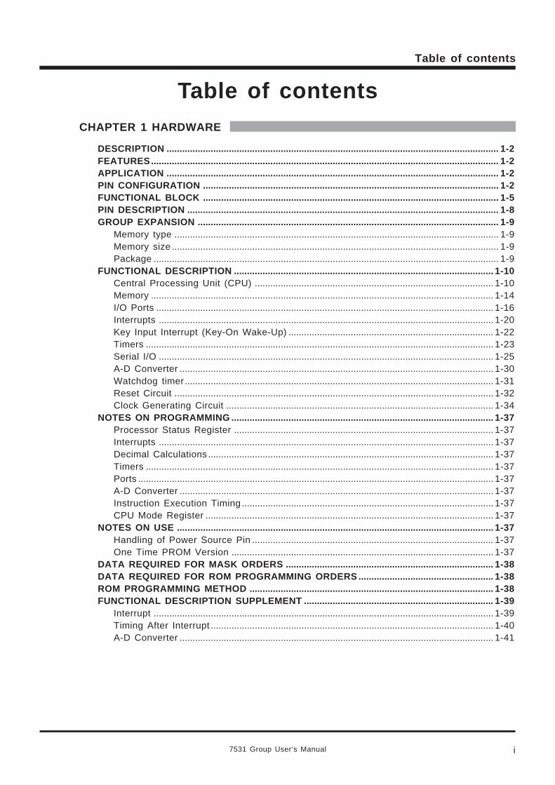
Table of contentsCHAPTER 1 HARDWARE
DESCRIPTION ................................................................................................................................ 1-2FEATURES ...................................................................................................................................... 1-2APPLICATION ................................................................................................................................ 1-2PIN CONFIGURATION .................................................................................................................. 1-2FUNCTIONAL BLOCK .................................................................................................................. 1-5PIN DESCRIPTION ........................................................................................................................ 1-8GROUP EXPANSION .................................................................................................................... 1-9
Memory type ............................................................................................................................. 1-9Memory size .............................................................................................................................. 1-9Package ..................................................................................................................................... 1-9
FUNCTIONAL DESCRIPTION .................................................................................................... 1-10Central Processing Unit (CPU) ............................................................................................ 1-10Memory .................................................................................................................................... 1-14I/O Ports .................................................................................................................................. 1-16Interrupts ................................................................................................................................. 1-20Key Input Interrupt (Key-On Wake-Up) ............................................................................... 1-22Timers ...................................................................................................................................... 1-23Serial I/O ................................................................................................................................. 1-25A-D Converter ......................................................................................................................... 1-30Watchdog timer....................................................................................................................... 1-31Reset Circuit ........................................................................................................................... 1-32Clock Generating Circuit ....................................................................................................... 1-34
NOTES ON PROGRAMMING ..................................................................................................... 1-37Processor Status Register .................................................................................................... 1-37Interrupts ................................................................................................................................. 1-37Decimal Calculations .............................................................................................................. 1-37Timers ...................................................................................................................................... 1-37Ports ......................................................................................................................................... 1-37A-D Converter ......................................................................................................................... 1-37Instruction Execution Timing ................................................................................................. 1-37CPU Mode Register ............................................................................................................... 1-37
NOTES ON USE .......................................................................................................................... 1-37Handling of Power Source Pin ............................................................................................. 1-37One Time PROM Version ..................................................................................................... 1-37
DATA REQUIRED FOR MASK ORDERS ................................................................................ 1-38DATA REQUIRED FOR ROM PROGRAMMING ORDERS .................................................... 1-38ROM PROGRAMMING METHOD .............................................................................................. 1-38FUNCTIONAL DESCRIPTION SUPPLEMENT ......................................................................... 1-39
Interrupt ................................................................................................................................... 1-39Timing After Interrupt ............................................................................................................. 1-40A-D Converter ......................................................................................................................... 1-41
7531 Group User’s Manualii
Table of contents
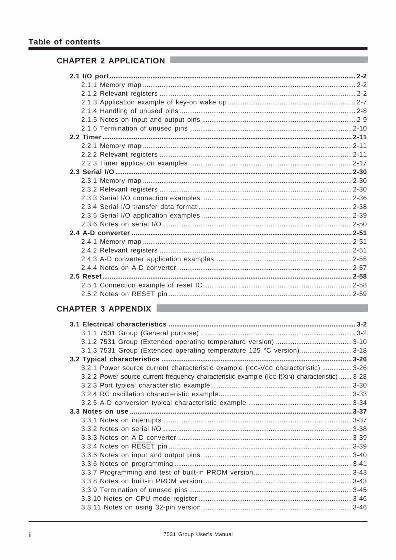
CHAPTER 2 APPLICATION
2.1 I/O port ..................................................................................................................................... 2-22.1.1 Memory map ................................................................................................................... 2-22.1.2 Relevant registers .......................................................................................................... 2-22.1.3 Application example of key-on wake up ..................................................................... 2-72.1.4 Handling of unused pins ............................................................................................... 2-82.1.5 Notes on input and output pins ................................................................................... 2-92.1.6 Termination of unused pins ........................................................................................ 2-10
2.2 Timer ....................................................................................................................................... 2-112.2.1 Memory map ................................................................................................................. 2-112.2.2 Relevant registers ........................................................................................................ 2-112.2.3 Timer application examples ........................................................................................ 2-17
2.3 Serial I/O ................................................................................................................................ 2-302.3.1 Memory map ................................................................................................................. 2-302.3.2 Relevant registers ........................................................................................................ 2-302.3.3 Serial I/O connection examples ................................................................................. 2-362.3.4 Serial I/O transfer data format ................................................................................... 2-382.3.5 Serial I/O application examples ................................................................................. 2-392.3.6 Notes on serial I/O ...................................................................................................... 2-50
2.4 A-D converter ....................................................................................................................... 2-512.4.1 Memory map ................................................................................................................. 2-512.4.2 Relevant registers ........................................................................................................ 2-512.4.3 A-D converter application examples .......................................................................... 2-552.4.4 Notes on A-D converter .............................................................................................. 2-57
2.5 Reset ....................................................................................................................................... 2-582.5.1 Connection example of reset IC ................................................................................ 2-582.5.2 Notes on RESET pin ................................................................................................... 2-59
CHAPTER 3 APPENDIX
3.1 Electrical characteristics ..................................................................................................... 3-23.1.1 7531 Group (General purpose) .................................................................................... 3-23.1.2 7531 Group (Extended operating temperature version) ......................................... 3-103.1.3 7531 Group (Extended operating temperature 125 °C version) ............................ 3-18
3.2 Typical characteristics ....................................................................................................... 3-263.2.1 Power source current characteristic example (ICC-VCC characteristic) ................ 3-263.2.2 Power source current frequency characteristic example (ICC-f(XIN) characteristic) ....... 3-283.2.3 Port typical characteristic example ............................................................................ 3-303.2.4 RC oscillation characteristic example........................................................................ 3-333.2.5 A-D conversion typical characteristic example ........................................................ 3-34
3.3 Notes on use ........................................................................................................................ 3-373.3.1 Notes on interrupts ...................................................................................................... 3-373.3.2 Notes on serial I/O ...................................................................................................... 3-383.3.3 Notes on A-D converter .............................................................................................. 3-393.3.4 Notes on RESET pin ................................................................................................... 3-393.3.5 Notes on input and output pins ................................................................................. 3-403.3.6 Notes on programming ................................................................................................ 3-413.3.7 Programming and test of built-in PROM version..................................................... 3-433.3.8 Notes on built-in PROM version ................................................................................ 3-433.3.9 Termination of unused pins ........................................................................................ 3-453.3.10 Notes on CPU mode register ................................................................................... 3-463.3.11 Notes on using 32-pin version ................................................................................. 3-46
7531 Group User’s Manual iii
Table of contents
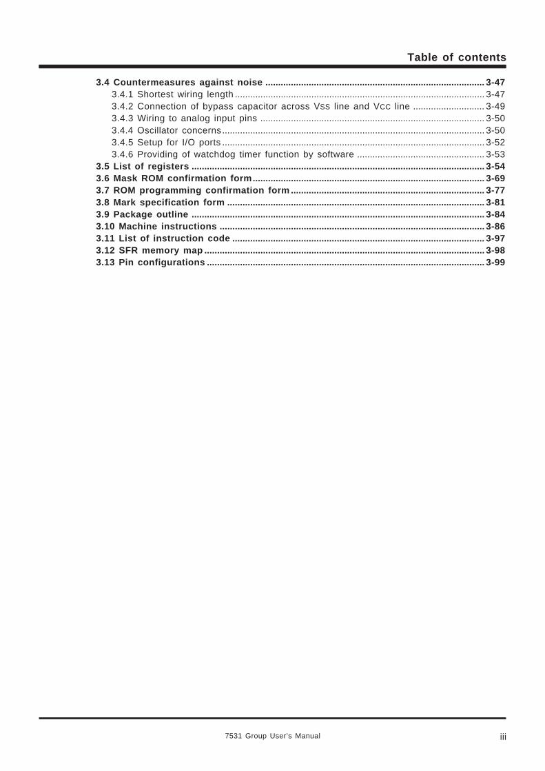
3.4 Countermeasures against noise ...................................................................................... 3-473.4.1 Shortest wiring length .................................................................................................. 3-473.4.2 Connection of bypass capacitor across VSS line and VCC line ............................ 3-493.4.3 Wiring to analog input pins ........................................................................................ 3-503.4.4 Oscillator concerns....................................................................................................... 3-503.4.5 Setup for I/O ports ....................................................................................................... 3-523.4.6 Providing of watchdog timer function by software .................................................. 3-53
3.5 List of registers ................................................................................................................... 3-543.6 Mask ROM confirmation form ........................................................................................... 3-693.7 ROM programming confirmation form ............................................................................ 3-773.8 Mark specification form ..................................................................................................... 3-813.9 Package outline ................................................................................................................... 3-843.10 Machine instructions ........................................................................................................ 3-863.11 List of instruction code ................................................................................................... 3-973.12 SFR memory map .............................................................................................................. 3-983.13 Pin configurations ............................................................................................................. 3-99
7531 Group User’s Manual i
List of figures
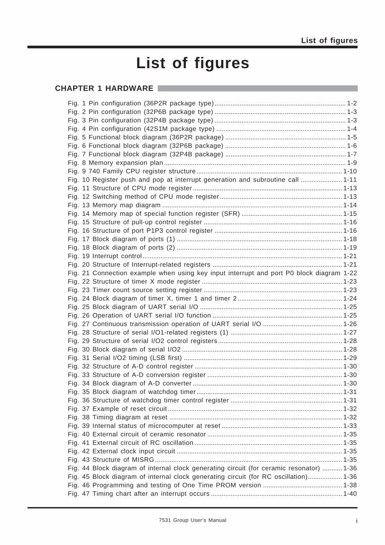
List of figuresCHAPTER 1 HARDWARE
Fig. 1 Pin configuration (36P2R package type) ......................................................................... 1-2Fig. 2 Pin configuration (32P6B package type) ......................................................................... 1-3Fig. 3 Pin configuration (32P4B package type) ......................................................................... 1-3Fig. 4 Pin configuration (42S1M package type) ........................................................................ 1-4Fig. 5 Functional block diagram (36P2R package) ................................................................... 1-5Fig. 6 Functional block diagram (32P6B package) ................................................................... 1-6Fig. 7 Functional block diagram (32P4B package) ................................................................... 1-7Fig. 8 Memory expansion plan ..................................................................................................... 1-9Fig. 9 740 Family CPU register structure ................................................................................. 1-10Fig. 10 Register push and pop at interrupt generation and subroutine call ....................... 1-11Fig. 11 Structure of CPU mode register ................................................................................... 1-13Fig. 12 Switching method of CPU mode register .................................................................... 1-13Fig. 13 Memory map diagram .................................................................................................... 1-14Fig. 14 Memory map of special function register (SFR) ........................................................ 1-15Fig. 15 Structure of pull-up control register ............................................................................. 1-16Fig. 16 Structure of port P1P3 control register ....................................................................... 1-16Fig. 17 Block diagram of ports (1) ............................................................................................ 1-18Fig. 18 Block diagram of ports (2) ............................................................................................ 1-19Fig. 19 Interrupt control ............................................................................................................... 1-21Fig. 20 Structure of Interrupt-related registers ........................................................................ 1-21Fig. 21 Connection example when using key input interrupt and port P0 block diagram 1-22Fig. 22 Structure of timer X mode register .............................................................................. 1-23Fig. 23 Timer count source setting register ............................................................................. 1-23Fig. 24 Block diagram of timer X, timer 1 and timer 2 .......................................................... 1-24Fig. 25 Block diagram of UART serial I/O ............................................................................... 1-25Fig. 26 Operation of UART serial I/O function ........................................................................ 1-25Fig. 27 Continuous transmission operation of UART serial I/O ............................................ 1-26Fig. 28 Structure of serial I/O1-related registers (1) .............................................................. 1-27Fig. 29 Structure of serial I/O2 control registers ..................................................................... 1-28Fig. 30 Block diagram of serial I/O2 ......................................................................................... 1-28Fig. 31 Serial I/O2 timing (LSB first) ........................................................................................ 1-29Fig. 32 Structure of A-D control register .................................................................................. 1-30Fig. 33 Structure of A-D conversion register ........................................................................... 1-30Fig. 34 Block diagram of A-D converter ................................................................................... 1-30Fig. 35 Block diagram of watchdog timer ................................................................................. 1-31Fig. 36 Structure of watchdog timer control register .............................................................. 1-31Fig. 37 Example of reset circuit ................................................................................................. 1-32Fig. 38 Timing diagram at reset ................................................................................................ 1-32Fig. 39 Internal status of microcomputer at reset ................................................................... 1-33Fig. 40 External circuit of ceramic resonator ........................................................................... 1-35Fig. 41 External circuit of RC oscillation .................................................................................. 1-35Fig. 42 External clock input circuit ............................................................................................ 1-35Fig. 43 Structure of MISRG ........................................................................................................ 1-35Fig. 44 Block diagram of internal clock generating circuit (for ceramic resonator) ........... 1-36Fig. 45 Block diagram of internal clock generating circuit (for RC oscillation)................... 1-36Fig. 46 Programming and testing of One Time PROM version ............................................ 1-38Fig. 47 Timing chart after an interrupt occurs ......................................................................... 1-40
7531 Group User’s Manualii
List of figures
Fig. 48 Time up to execution of the interrupt processing routine ........................................ 1-40Fig. 49 A-D conversion equivalent circuit ................................................................................. 1-42Fig. 50 A-D conversion timing chart .......................................................................................... 1-42
CHAPTER 2 APPLICATION
Fig. 2.1.1 Memory map of registers relevant to I/O port ......................................................... 2-2Fig. 2.1.2 Structure of Port Pi (i = 0, 2, 3) ................................................................................ 2-2Fig. 2.1.3 Structure of Port P1..................................................................................................... 2-3Fig. 2.1.4 Structure of Port Pi direction register (i = 0, 2, 3) ................................................. 2-3Fig. 2.1.5 Structure of Port P1 direction register ...................................................................... 2-4Fig. 2.1.6 Structure of Pull-up control register .......................................................................... 2-4Fig. 2.1.7 Structure of Interrupt edge selection register .......................................................... 2-5Fig. 2.1.8 Structure of Interrupt request register 1 ................................................................... 2-5Fig. 2.1.9 Structure of Interrupt control register 1 .................................................................... 2-6Fig. 2.1.10 Relevant registers setting ......................................................................................... 2-7Fig. 2.1.11 Application circuit example ....................................................................................... 2-7Fig. 2.1.12 Control procedure....................................................................................................... 2-8Fig. 2.2.1 Memory map of registers relevant to timers .......................................................... 2-11Fig. 2.2.2 Structure of Prescaler 12, Prescaler X ................................................................... 2-11Fig. 2.2.3 Structure of Timer 1 .................................................................................................. 2-12Fig. 2.2.4 Structure of Timer 2 .................................................................................................. 2-12Fig. 2.2.5 Structure of Timer X .................................................................................................. 2-13Fig. 2.2.6 Structure of Timer X mode register......................................................................... 2-14Fig. 2.2.7 Structure of Timer count source set register ......................................................... 2-15Fig. 2.2.8 Structure of Interrupt edge selection register ........................................................ 2-15Fig. 2.2.9 Structure of Interrupt request register 1 ................................................................. 2-16Fig. 2.2.10 Structure of Interrupt control register 1 ................................................................ 2-16Fig. 2.2.11 Timers connection and setting of division ratios ................................................. 2-18Fig. 2.2.12 Relevant registers setting ....................................................................................... 2-19Fig. 2.2.13 Control procedure..................................................................................................... 2-20Fig. 2.2.14 Peripheral circuit example....................................................................................... 2-21Fig. 2.2.15 Timers connection and setting of division ratios ................................................. 2-21Fig. 2.2.16 Relevant registers setting ....................................................................................... 2-22Fig. 2.2.17 Control procedure..................................................................................................... 2-23Fig 2.2.18 Judgment method of valid/invalid of input pulses ................................................ 2-24Fig. 2.2.19 Relevant registers setting ....................................................................................... 2-25Fig. 2.2.20 Control procedure..................................................................................................... 2-26Fig. 2.2.21 Timers connection and setting of division ratios ................................................. 2-27Fig. 2.2.22 Relevant registers setting ....................................................................................... 2-28Fig. 2.2.23 Control procedure..................................................................................................... 2-29Fig. 2.3.1 Memory map of registers relevant to serial I/O..................................................... 2-30Fig. 2.3.2 Structure of Transmit/Receive buffer register ........................................................ 2-30Fig. 2.3.3 Structure of Serial I/O1 status register ................................................................... 2-31Fig. 2.3.4 Structure of Serial I/O1 control register .................................................................. 2-31Fig. 2.3.5 Structure of UART control register .......................................................................... 2-32Fig. 2.3.6 Structure of Baud rate generator ............................................................................. 2-32Fig. 2.3.7 Structure of Serial I/O2 control register .................................................................. 2-33Fig. 2.3.8 Structure of Serial I/O2 register ............................................................................... 2-33Fig. 2.3.9 Structure of Interrupt edge selection register ........................................................ 2-34Fig. 2.3.10 Structure of Interrupt request register 1 ............................................................... 2-34Fig. 2.3.11 Structure of Interrupt control register 1 ................................................................ 2-35
7531 Group User’s Manual iii
List of figures
Fig. 2.3.12 Serial I/O connection examples (1) ....................................................................... 2-36Fig. 2.3.13 Serial I/O connection examples (2) ....................................................................... 2-37Fig. 2.3.14 Serial I/O transfer data format ............................................................................... 2-38Fig. 2.3.15 Connection diagram ................................................................................................. 2-39Fig. 2.3.16 Timing chart .............................................................................................................. 2-39Fig. 2.3.17 Registers setting relevant to transmission side ................................................... 2-40Fig. 2.3.18 Transmission data setting of serial I/O2............................................................... 2-41Fig. 2.3.19 Registers setting relevant to reception side ......................................................... 2-41Fig. 2.3.20 Control procedure of transmission side ................................................................ 2-42Fig. 2.3.21 Control procedure of reception side ...................................................................... 2-43Fig. 2.3.22 Connection diagram ................................................................................................. 2-44Fig. 2.3.23 Timing chart .............................................................................................................. 2-44Fig. 2.3.24 Registers setting relevant to transmission side ................................................... 2-46Fig. 2.3.25 Registers setting relevant to reception side ......................................................... 2-47Fig. 2.3.26 Control procedure of transmission side ................................................................ 2-48Fig. 2.3.27 Control procedure of reception side ...................................................................... 2-49Fig. 2.3.28 Sequence of clearing serial I/O ............................................................................. 2-50Fig. 2.4.1 Memory map of registers relevant to A-D converter ............................................ 2-51Fig. 2.4.2 Structure of A-D control register .............................................................................. 2-51Fig. 2.4.3 Structure of A-D conversion register (high-order) ................................................. 2-52Fig. 2.4.4 Structure of A-D conversion register (low-order) ................................................... 2-52Fig. 2.4.5 Structure of Interrupt edge selection register ........................................................ 2-53Fig. 2.4.6 Structure of Interrupt request register 1 ................................................................. 2-53Fig. 2.4.7 Structure of Interrupt control register 1 .................................................................. 2-54Fig. 2.4.8 Connection diagram ................................................................................................... 2-55Fig. 2.4.9 Relevant registers setting ......................................................................................... 2-55Fig. 2.4.10 Control procedure for 8-bit read ............................................................................ 2-56Fig. 2.4.11 Control procedure for 10-bit read .......................................................................... 2-56Fig. 2.5.1 Example of poweron reset circuit ............................................................................ 2-58Fig. 2.5.2 RAM backup system .................................................................................................. 2-58
CHAPTER 3 APPENDIX
Fig. 3.1.1 Switching characteristics measurement circuit diagram (General purpose)......... 3-8Fig. 3.1.2 Timing chart (General purpose) ................................................................................. 3-9Fig. 3.1.3 Switching characteristics measurement circuit diagram
(Extended operating temperature version) .............................................................. 3-16Fig. 3.1.4 Timing chart (Extended operating temperature version) ...................................... 3-17Fig. 3.1.5 Switching characteristics measurement circuit diagram
(Extended operating temperature 125 °C version) ................................................ 3-24Fig. 3.1.6 Timing chart (Extended operating temperature 125 °C version) ......................... 3-25Fig. 3.2.1 ICC-VCC characteristic example (in double-speed mode) ..................................... 3-26Fig. 3.2.2 ICC-VCC characteristic example (in high-speed mode) ......................................... 3-26Fig. 3.2.3 ICC-VCC characteristic example (in middle-speed mode) ..................................... 3-26Fig. 3.2.4 ICC-VCC characteristic example (in wait mode) ..................................................... 3-27Fig. 3.2.5 ICC-VCC characteristic example (in stop mode) ..................................................... 3-27Fig. 3.2.6 ICC-VCC characteristic example (addition when operating A-D conversion, A-D conversion
executed/not executed, f(XIN) = 8MHz, in high-speed mode) .............................. 3-27Fig. 3.2.7 ICC-f(XIN) characteristic example (in double-speed mode) ................................... 3-28Fig. 3.2.8 ICC-f(XIN) characteristic example (in high-speed mode) ....................................... 3-28Fig. 3.2.9 ICC-f(XIN) characteristic example (in middle-speed mode) ................................... 3-28Fig. 3.2.10 ICC-f(XIN) characteristic example (in wait mode) ................................................. 3-29
7531 Group User’s Manualiv
List of figures
Fig. 3.2.11 VOH-IOH characteristic example of P-channel (Ta = 25 °C): normal port ........ 3-30Fig. 3.2.12 VOH-IOH characteristic example of P-channel (Ta = 90 °C): normal port ........ 3-30Fig. 3.2.13 VOL-IOL characteristic example of N-channel (Ta = 25 °C): normal port ........ 3-31Fig. 3.2.14 VOL-IOL characteristic example of N-channel (Ta = 90 °C): normal port ........ 3-31Fig. 3.2.15 VOL-IOL characteristic example of N-channel (Ta = 25 °C): LED drive port ... 3-32Fig. 3.2.16 VOL-IOL characteristic example of N-channel (Ta = 90 °C): LED drive port ... 3-32Fig. 3.2.17 “L” input current when connecting pull-up transistor .......................................... 3-33Fig. 3.2.18 RC oscillation characteristic example.................................................................... 3-33Fig. 3.2.19 Definition of A-D conversion accuracy .................................................................. 3-34Fig. 3.2.20 A-D conversion accuracy typical characteristic example-1 ................................ 3-35Fig. 3.2.21 A-D conversion accuracy typical characteristic example-2 ................................ 3-36Fig. 3.3.1 Sequence of switch the detection edge .................................................................. 3-37Fig. 3.3.2 Sequence of check of interrupt request bit ............................................................ 3-37Fig. 3.3.3 Structure of interrupt control register 1 .................................................................. 3-38Fig. 3.3.4 Sequence of clearing serial I/O ............................................................................... 3-38Fig. 3.3.5 Initialization of processor status register ................................................................ 3-41Fig. 3.3.6 Sequence of PLP instruction execution .................................................................. 3-41Fig. 3.3.7 Stack memory contents after PHP instruction execution ..................................... 3-41Fig. 3.3.8 Status flag at decimal calculations .......................................................................... 3-42Fig. 3.3.9 Programming and testing of One Time PROM version ........................................ 3-43Fig. 3.3.10 Switching method of CPU mode register ............................................................. 3-46Fig. 3.4.1 Selection of packages ............................................................................................... 3-47Fig. 3.4.2 Wiring for the RESET pin ......................................................................................... 3-47Fig. 3.4.3 Wiring for clock I/O pins ........................................................................................... 3-48Fig. 3.4.4 Wiring for CNVSS pin ............................................................................................... 3-48Fig. 3.4.5 Wiring for the VPP pin of the One Time PROM and the EPROM version ........ 3-49Fig. 3.4.6 Bypass capacitor across the VSS line and the VCC line ...................................... 3-49Fig. 3.4.7 Analog signal line and a resistor and a capacitor ................................................ 3-50Fig. 3.4.8 Wiring for a large current signal line ...................................................................... 3-50Fig. 3.4.9 Wiring of signal lines where potential levels change frequently ......................... 3-51Fig. 3.4.10 VSS pattern on the underside of an oscillator ..................................................... 3-51Fig. 3.4.11 Setup for I/O ports ................................................................................................... 3-52Fig. 3.4.12 Watchdog timer by software ................................................................................... 3-53Fig. 3.5.1 Structure of Port Pi (i = 0, 2, 3) .............................................................................. 3-54Fig. 3.5.2 Structure of Port P1................................................................................................... 3-54Fig. 3.5.3 Structure of Port Pi direction register (i = 0, 2, 3) ............................................... 3-55Fig. 3.5.4 Structure of Port P1 direction register .................................................................... 3-55Fig. 3.5.5 Structure of Pull-up control register ........................................................................ 3-56Fig. 3.5.6 Structure of Port P1P3 control register .................................................................. 3-56Fig. 3.5.7 Structure of Transmit/Receive buffer register ........................................................ 3-57Fig. 3.5.8 Structure of Serial I/O1 status register ................................................................... 3-57Fig. 3.5.9 Structure of Serial I/O1 control register .................................................................. 3-58Fig. 3.5.10 Structure of UART control register ........................................................................ 3-58Fig. 3.5.11 Structure of Baud rate generator ........................................................................... 3-59Fig. 3.5.12 Structure of Prescaler 12, Prescaler X ................................................................. 3-59Fig. 3.5.13 Structure of Timer 1 ................................................................................................ 3-60Fig. 3.5.14 Structure of Timer 2 ................................................................................................ 3-60Fig. 3.5.15 Structure of Timer X mode register ...................................................................... 3-61Fig. 3.5.16 Structure of Timer X ................................................................................................ 3-62Fig. 3.5.17 Structure of Timer count source set register ....................................................... 3-62Fig. 3.5.18 Structure of Serial I/O2 control register ................................................................ 3-63Fig. 3.5.19 Structure of Serial I/O2 register ............................................................................. 3-63
7531 Group User’s Manual v
List of figures
Fig. 3.5.20 Structure of A-D control register ............................................................................ 3-64Fig. 3.5.21 Structure of A-D conversion register (low-order) ................................................. 3-64Fig. 3.5.22 Structure of A-D conversion register (high-order) ............................................... 3-65Fig. 3.5.23 Structure of MISRG ................................................................................................. 3-65Fig. 3.5.24 Structure of Watchdog timer control register ....................................................... 3-66Fig. 3.5.25 Structure of Interrupt edge selection register ...................................................... 3-66Fig. 3.5.26 Structure of CPU mode register ............................................................................ 3-67Fig. 3.5.27 Structure of Interrupt request register 1 ............................................................... 3-67Fig. 3.5.28 Structure of Interrupt control register 1 ................................................................ 3-68Fig. 3.13.1 Pin configuration (36P2R package type) .............................................................. 3-99Fig. 3.13.2 Pin configuration (32P6B package type) ............................................................ 3-100Fig. 3.13.3 Pin configuration (32P4B package type) ............................................................ 3-101Fig. 3.13.4 M37531RSS pin configuration .............................................................................. 3-102
7531 Group User’s Manual i
List of tables
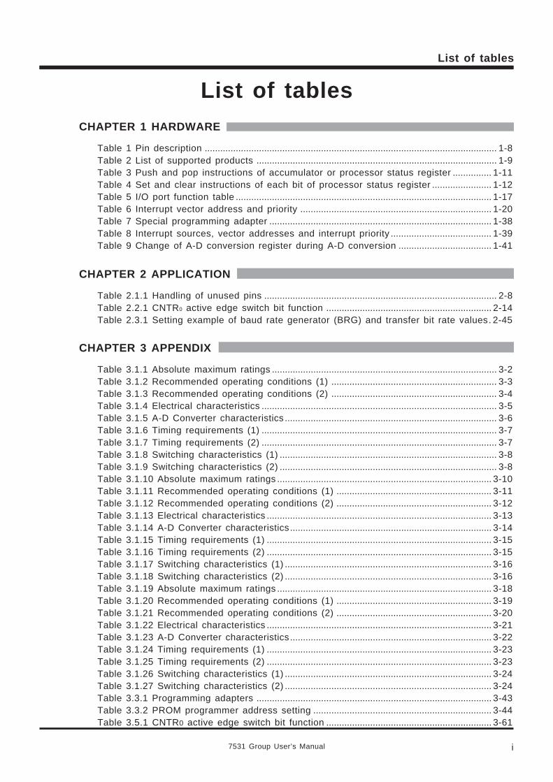
List of tablesCHAPTER 1 HARDWARE
Table 1 Pin description ................................................................................................................. 1-8Table 2 List of supported products ............................................................................................. 1-9Table 3 Push and pop instructions of accumulator or processor status register ............... 1-11Table 4 Set and clear instructions of each bit of processor status register ....................... 1-12Table 5 I/O port function table ................................................................................................... 1-17Table 6 Interrupt vector address and priority .......................................................................... 1-20Table 7 Special programming adapter ...................................................................................... 1-38Table 8 Interrupt sources, vector addresses and interrupt priority ....................................... 1-39Table 9 Change of A-D conversion register during A-D conversion .................................... 1-41
CHAPTER 2 APPLICATION
Table 2.1.1 Handling of unused pins .......................................................................................... 2-8Table 2.2.1 CNTR0 active edge switch bit function ................................................................ 2-14Table 2.3.1 Setting example of baud rate generator (BRG) and transfer bit rate values. 2-45
CHAPTER 3 APPENDIX
Table 3.1.1 Absolute maximum ratings ....................................................................................... 3-2Table 3.1.2 Recommended operating conditions (1) ................................................................ 3-3Table 3.1.3 Recommended operating conditions (2) ................................................................ 3-4Table 3.1.4 Electrical characteristics ........................................................................................... 3-5Table 3.1.5 A-D Converter characteristics .................................................................................. 3-6Table 3.1.6 Timing requirements (1) ........................................................................................... 3-7Table 3.1.7 Timing requirements (2) ........................................................................................... 3-7Table 3.1.8 Switching characteristics (1) .................................................................................... 3-8Table 3.1.9 Switching characteristics (2) .................................................................................... 3-8Table 3.1.10 Absolute maximum ratings ................................................................................... 3-10Table 3.1.11 Recommended operating conditions (1) ............................................................ 3-11Table 3.1.12 Recommended operating conditions (2) ............................................................ 3-12Table 3.1.13 Electrical characteristics ....................................................................................... 3-13Table 3.1.14 A-D Converter characteristics.............................................................................. 3-14Table 3.1.15 Timing requirements (1) ....................................................................................... 3-15Table 3.1.16 Timing requirements (2) ....................................................................................... 3-15Table 3.1.17 Switching characteristics (1) ................................................................................ 3-16Table 3.1.18 Switching characteristics (2) ................................................................................ 3-16Table 3.1.19 Absolute maximum ratings ................................................................................... 3-18Table 3.1.20 Recommended operating conditions (1) ............................................................ 3-19Table 3.1.21 Recommended operating conditions (2) ............................................................ 3-20Table 3.1.22 Electrical characteristics ....................................................................................... 3-21Table 3.1.23 A-D Converter characteristics.............................................................................. 3-22Table 3.1.24 Timing requirements (1) ....................................................................................... 3-23Table 3.1.25 Timing requirements (2) ....................................................................................... 3-23Table 3.1.26 Switching characteristics (1) ................................................................................ 3-24Table 3.1.27 Switching characteristics (2) ................................................................................ 3-24Table 3.3.1 Programming adapters ........................................................................................... 3-43Table 3.3.2 PROM programmer address setting ..................................................................... 3-44Table 3.5.1 CNTR0 active edge switch bit function ................................................................ 3-61
CHAPTER 1HARDWARE
DESCRIPTIONFEATURESAPPLICATIONPIN CONFIGURATIONFUNCTIONAL BLOCKPIN DESCRIPTIONGROUP EXPANSIONFUNCTIONAL DESCRIPTIONNOTES ON PROGRAMMINGNOTES ON USEDATA REQUIRED FOR MASK ORDERSDATA REQUIRED FOR ROM PROGRAMMING ORDERSROM PROGRAMMING METHODFUNCTIONAL DESCRIPTION SUPPLEMENT
HARDWARE
7531 Group User’s Manual1-2
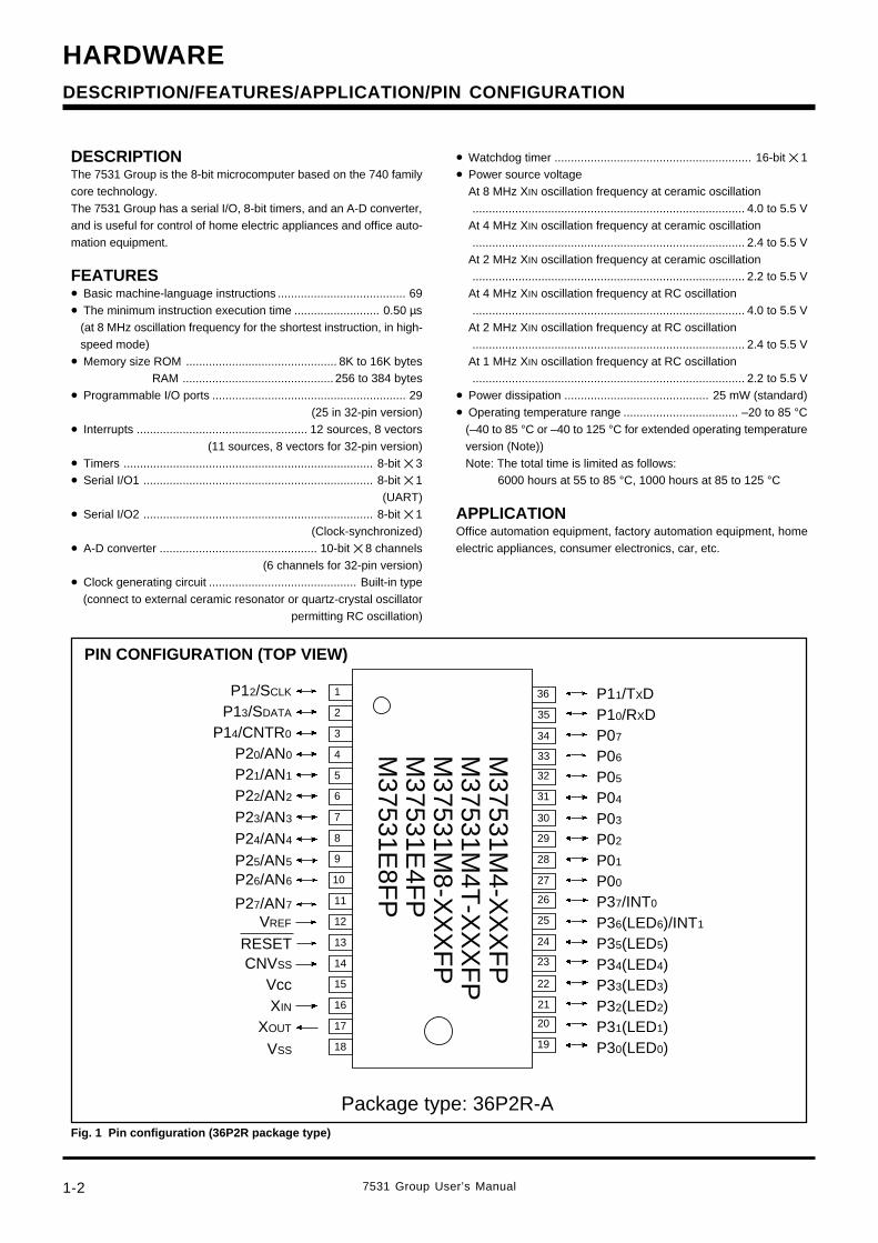
DESCRIPTIONThe 7531 Group is the 8-bit microcomputer based on the 740 familycore technology.The 7531 Group has a serial I/O, 8-bit timers, and an A-D converter,and is useful for control of home electric appliances and office auto-mation equipment.
FEATURES• Basic machine-language instructions ....................................... 69
• The minimum instruction execution time .......................... 0.50 µs(at 8 MHz oscillation frequency for the shortest instruction, in high-speed mode)
• Memory size ROM .............................................. 8K to 16K bytesRAM .............................................. 256 to 384 bytes
• Programmable I/O ports ........................................................... 29(25 in 32-pin version)
• Interrupts .................................................... 12 sources, 8 vectors(11 sources, 8 vectors for 32-pin version)
• Timers ............................................................................ 8-bit 3
• Serial I/O1 ...................................................................... 8-bit 1(UART)
• Serial I/O2 ...................................................................... 8-bit 1(Clock-synchronized)
• A-D converter ................................................ 10-bit 8 channels(6 channels for 32-pin version)
• Clock generating circuit ............................................. Built-in type(connect to external ceramic resonator or quartz-crystal oscillator
permitting RC oscillation)
• Watchdog timer ............................................................ 16-bit 1
• Power source voltageAt 8 MHz XIN oscillation frequency at ceramic oscillation................................................................................... 4.0 to 5.5 V
At 4 MHz XIN oscillation frequency at ceramic oscillation................................................................................... 2.4 to 5.5 V
At 2 MHz XIN oscillation frequency at ceramic oscillation................................................................................... 2.2 to 5.5 V
At 4 MHz XIN oscillation frequency at RC oscillation................................................................................... 4.0 to 5.5 V
At 2 MHz XIN oscillation frequency at RC oscillation................................................................................... 2.4 to 5.5 V
At 1 MHz XIN oscillation frequency at RC oscillation................................................................................... 2.2 to 5.5 V
• Power dissipation ............................................ 25 mW (standard)
• Operating temperature range ................................... –20 to 85 °C(–40 to 85 °C or –40 to 125 °C for extended operating temperatureversion (Note))Note: The total time is limited as follows:
6000 hours at 55 to 85 °C, 1000 hours at 85 to 125 °C
APPLICATIONOffice automation equipment, factory automation equipment, homeelectric appliances, consumer electronics, car, etc.
PIN CONFIGURATION (TOP VIEW)
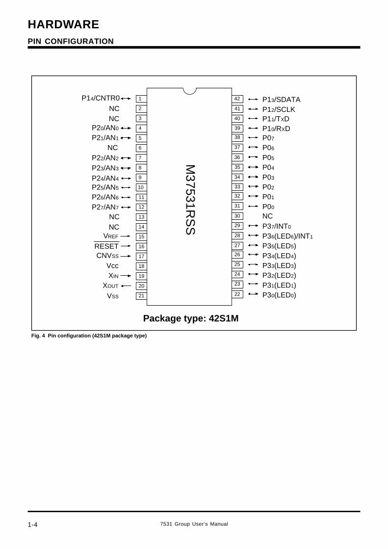
Fig. 1 Pin configuration (36P2R package type)
Package type: 36P2R-A
10
1
2
3
4
6
7
8
9
11
12
14
15
16
5
13
17
18
36
35
34
33
31
30
26
25
24
23
22
21
20
19
32
27
29
28
P00
CNVSS
XOUT
XIN
VSS
P01
P02
P03
P04
P30(LED0)
Vcc
VREF
P05
P10/RXD
P26/AN6
P27/AN7
P11/TXDP12/SCLK
P13/SDATA
P23/AN3
P22/AN2
P21/AN1
P20/AN0
P31(LED1)
P36(LED6)/INT1
P24/AN4
P25/AN5
P06
P07
P37/INT0
RESET
M37531M
4-XX
XF
PM
37531M4T
-XX
XF
PM
37531M8-X
XX
FP
M37531E
4FP
M37531E
8FP
P14/CNTR0
P35(LED5)P34(LED4)P33(LED3)P32(LED2)
DESCRIPTION/FEATURES/APPLICATION/PIN CONFIGURATION
7531 Group User’s Manual 1-3
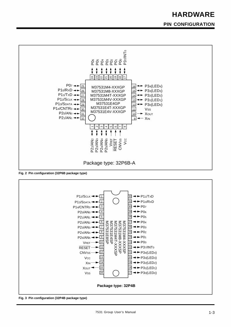
HARDWARE
Fig. 3 Pin configuration (32P4B package type)
Fig. 2 Pin configuration (32P6B package type)
Package type: 32P6B-A
P07
P10/RXDP11/TXDP12/SCLK
P13/SDATA
P14/CNTR0
P20/AN0
P21/AN1 32
31
30
29
28
27
26
25 P34(LED4)P33(LED3)P32(LED2)P31(LED1)P30(LED0)VSS
XOUT
XIN9
10
11
12
13
14
15
16
2 876531 4
VC
C
CN
VS
S
RE
SE
T
P22
/AN
2
P05
20 1718192124
P02
P04
P03
P06
23 22
P01
P00
P37
/INT
0
M37531M4-XXXGPM37531M8-XXXGP
M37531M4T-XXXGPM37531M4V-XXXGP
M37531E4GPM37531E4T-XXXGPM37531E4V-XXXGP
P23
/AN
3
P24
/AN
4
P25
/AN
5
VR
EF
1
2
3
4
5
6
7
8
9
10
11
12
13
14
15
16
CNVSS
P12/SCLK
P13/SDATA
P14/CNTR0
P20/AN0
P21/AN1
P22/AN2
P23/AN3
P24/AN4
VCC
XIN
XOUT
VSS
P11/TXD
P10/RXD
P07
P06
P05
P04
P30(LED0)
P25/AN5
VREF
RESET
P00
P33(LED3)
P32(LED2)
P31(LED1)
M37531M
4-XX
XS
PM
37531M8-X
XX
SP
M37531M
4T-X
XX
SP
M37531E
4SP
M37531E
8SP
32
P01
P02
P03
14
15
16
P37/INT0
P34(LED4)
17
18
19
20
21
22
23
24
25
26
27
28
29
30
31
Package type: 32P4B
PIN CONFIGURATION
HARDWARE
7531 Group User’s Manual1-4
Fig. 4 Pin configuration (42S1M package type)
10
1
2
3
4
6
7
8
9
11
12
14
15
16
5
13
17
18
36
35
34
33
31
30
26
25
24
23
22
32
27
29
28
19
20
21
42
41
40
39
37
38
P00
CNVSS
XOUT
XIN
VSS
P01
P02
P03
P04
P30(LED0)
Vcc
VREF
P05
P12/SCLK
P25/AN5
P26/AN6
P13/SDATAP14/CNTR0
NC
P22/AN2
NCP21/AN1
P20/AN0
P31(LED1)
P36(LED6)/INT1
P23/AN3
P24/AN4
P06
P07
P37/INT0
RESET
M37531R
SS
NC
P35(LED5)P34(LED4)P33(LED3)P32(LED2)
NC
P10/RXDP11/TXD
NCNC
P27/AN7
Package type: 42S1M
PIN CONFIGURATION
7531 Group User’s Manual 1-5
HARDWARE
FUNCTIONAL BLOCK
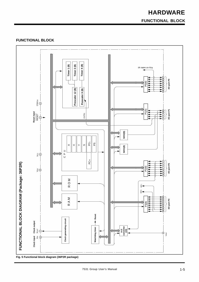
Fig. 5 Functional block diagram (36P2R package)
FU
NC
TIO
NA
L B
LOC
K D
IAG
RA
M (
Pac
kage
: 36P
2R)
R
A M
R
O M
C P
U
A X Y S
PC
HP
CL
PS
VS
S
1813
VC
C
1514
CN
TR
0
P0(
8)
3432
3028
3331
2927
P1(
5)
31
352
367
56
4
P2(
8)P
3(8)
2023
2119
12
1617
119
108
VR
EF
0
22
INT
0
2624
25
INT
1
RE
SE
TC
NV
SS
SI/O
2(8)
XIN
XO
UT
Clo
ck in
pu
tC
lock
ou
tpu
t
Clo
ck g
ener
atin
g c
ircu
it
Wat
chd
og
tim
erR
eset
A-D
co
nve
rter
(10)
I/O p
ort
P0
Tim
er 1
(8)
Tim
er 2
(8)
Tim
er X
(8)
Pre
scal
er 1
2 (8
)
Pre
scal
er X
(8)
Res
et in
pu
t
I/O p
ort
P1
I/O p
ort
P2
I/O p
ort
P3
SI/O
1(8)
Key-on wake up
FUNCTIONAL BLOCK
HARDWARE
7531 Group User’s Manual1-6
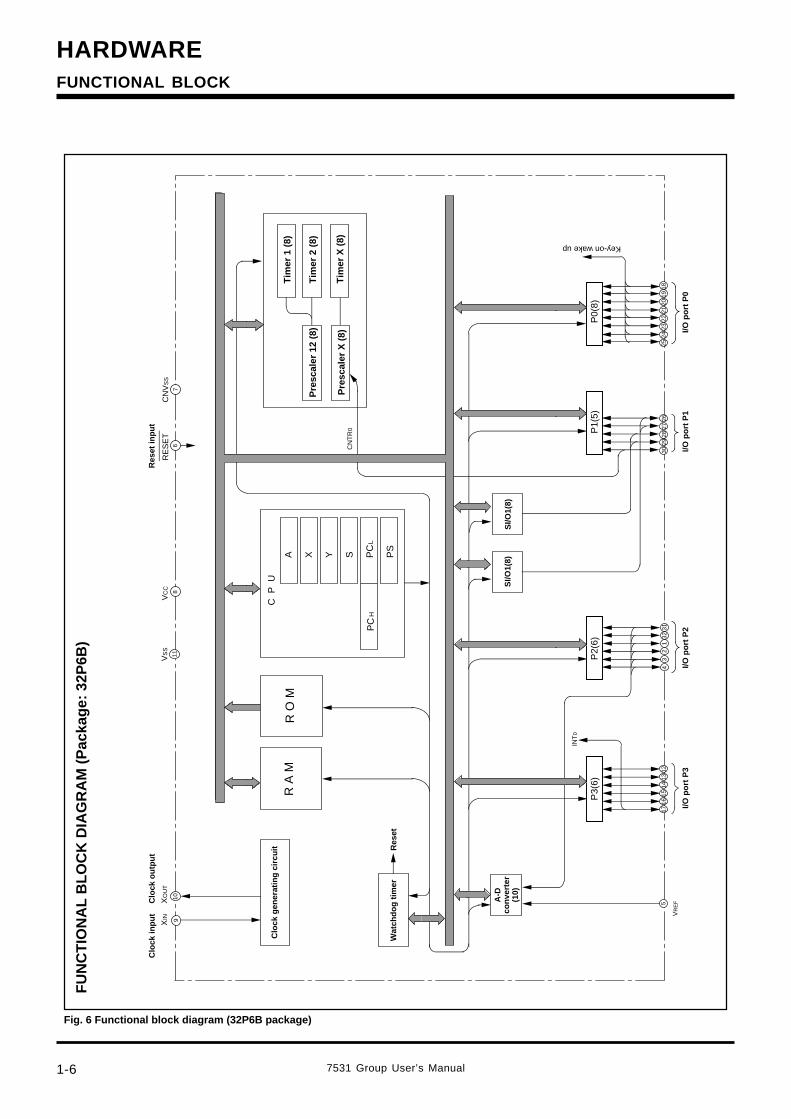
Fig. 6 Functional block diagram (32P6B package)
FU
NC
TIO
NA
L B
LOC
K D
IAG
RA
M (
Pac
kage
: 32P
6B)
FUNCTIONAL BLOCK
R
A M
R
O M
C P
U
A X Y S
PC
HP
CL
PS
VS
S
116
VC
C 87
CN
TR
0
P0(
8)
2523
2119
2422
2018
P1(
5)
3028
2629
2732
31
P2(
6)P
3(6)
1215
135
910
42
31
VR
EF
0
14
INT
0
1617
XIN
XO
UT
Clo
ck in
pu
tC
lock
ou
tpu
t
Clo
ck g
ener
atin
g c
ircu
it
I/O p
ort
P0
Tim
er 1
(8)
Tim
er 2
(8)
Tim
er X
(8)
Pre
scal
er 1
2 (8
)
Pre
scal
er X
(8)
RE
SE
TC
NV
SS
Res
et in
pu
t
Wat
chd
og
tim
erR
eset
A-D
co
nve
rter
(10)
SI/O
1(8)
Key-on wake up
I/O p
ort
P1
I/O p
ort
P2
I/O p
ort
P3
SI/O
1(8)
7531 Group User’s Manual 1-7
HARDWARE
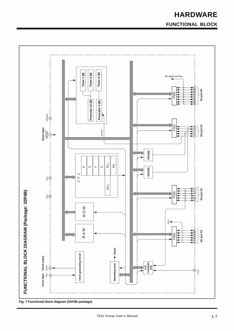
Fig. 7 Functional block diagram (32P4B package)
FU
NC
TIO
NA
L B
LOC
K D
IAG
RA
M (
Pac
kage
: 32P
4B)
FUNCTIONAL BLOCK
R
A M
R
O M
C P
U
A X Y S
PC
HP
CL
PS
VS
S
1611
VC
C
1312
CN
TR
0
P0(
8)
3028
2624
2927
2523
P1(
5)
31
312
325
4
P2(
6)P
3(6)
1720
1810
1415
97
86
VR
EF
0
19
INT
0
2122
XIN
XO
UT
Clo
ck in
pu
tC
lock
ou
tpu
t
Clo
ck g
ener
atin
g c
ircu
it
I/O p
ort
P0
Tim
er 1
(8)
Tim
er 2
(8)
Tim
er X
(8)
Pre
scal
er 1
2 (8
)
Pre
scal
er X
(8)
RE
SE
TC
NV
SS
Res
et in
pu
t
Wat
chd
og
tim
erR
eset
A-D
co
nve
rter
(10)
Key-on wake up
SI/O
1(8)
I/O p
ort
P1
SI/O
2(8)
I/O p
ort
P2
I/O p
ort
P3
HARDWARE
7531 Group User’s Manual1-8
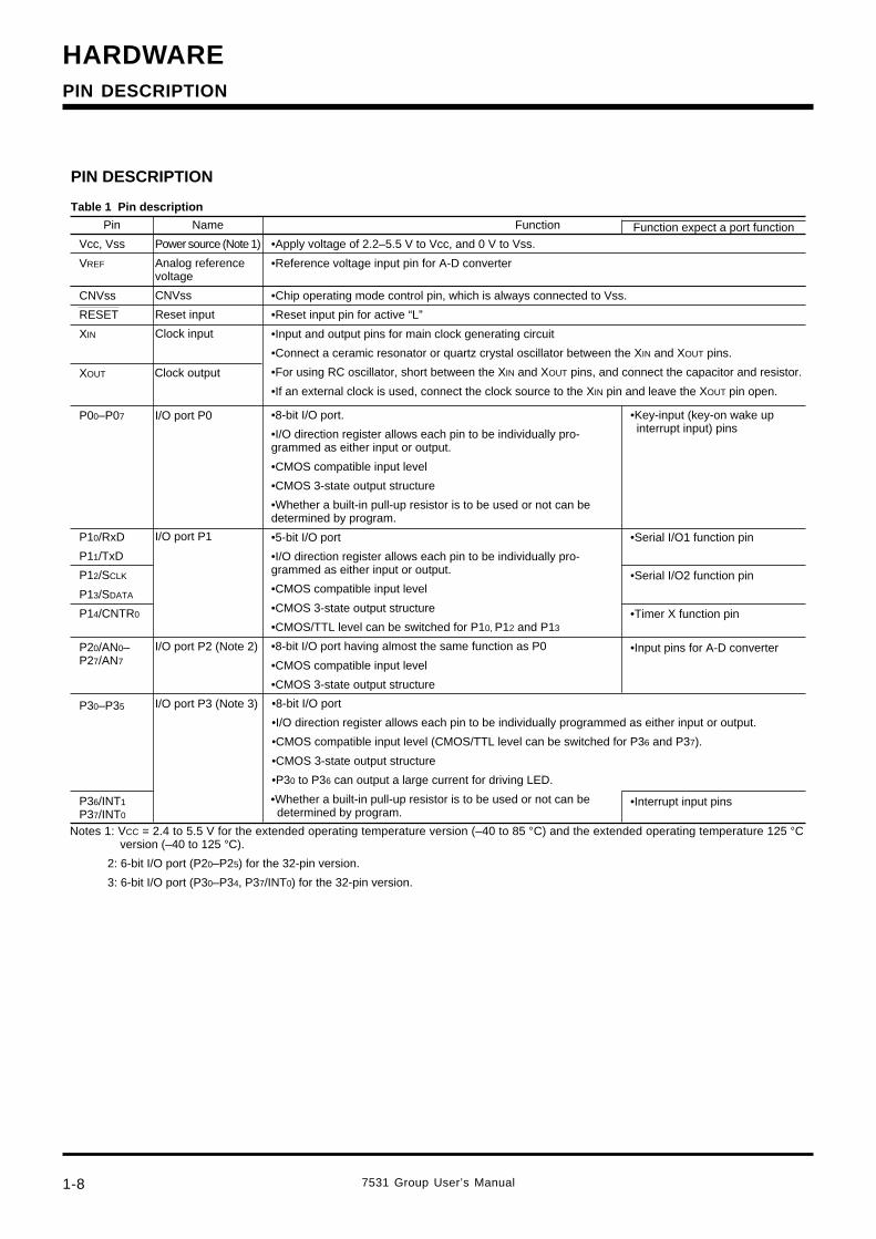
PIN DESCRIPTION
Table 1 Pin description
Function
•Apply voltage of 2.2–5.5 V to Vcc, and 0 V to Vss.
•Reference voltage input pin for A-D converter
•Chip operating mode control pin, which is always connected to Vss.
•Reset input pin for active “L”
•Input and output pins for main clock generating circuit
•Connect a ceramic resonator or quartz crystal oscillator between the XIN and XOUT pins.
•For using RC oscillator, short between the XIN and XOUT pins, and connect the capacitor and resistor.
•If an external clock is used, connect the clock source to the XIN pin and leave the XOUT pin open.
Function expect a port functionName
Power source (Note 1)
Analog referencevoltage
CNVss
Reset input
Clock input
Pin
Vcc, Vss
VREF
CNVss
RESET
XIN
P00–P07
P10/RxD
P11/TxD
P12/SCLK
P13/SDATA
P14/CNTR0
P20/AN0–P27/AN7
P30–P35
P36/INT1
P37/INT0
I/O port P0
I/O port P1
I/O port P2 (Note 2)
I/O port P3 (Note 3)
•8-bit I/O port.
•I/O direction register allows each pin to be individually pro-grammed as either input or output.
•CMOS compatible input level
•CMOS 3-state output structure
•Whether a built-in pull-up resistor is to be used or not can bedetermined by program.
•5-bit I/O port
•I/O direction register allows each pin to be individually pro-grammed as either input or output.
•CMOS compatible input level
•CMOS 3-state output structure
•CMOS/TTL level can be switched for P10, P12 and P13
•8-bit I/O port having almost the same function as P0
•CMOS compatible input level
•CMOS 3-state output structure
•8-bit I/O port
•I/O direction register allows each pin to be individually programmed as either input or output.
•CMOS compatible input level (CMOS/TTL level can be switched for P36 and P37).
•CMOS 3-state output structure
•P30 to P36 can output a large current for driving LED.
•Key-input (key-on wake upinterrupt input) pins
•Serial I/O1 function pin
•Serial I/O2 function pin
•Timer X function pin
•Input pins for A-D converter
•Interrupt input pins•Whether a built-in pull-up resistor is to be used or not can bedetermined by program.
XOUT Clock output
PIN DESCRIPTION
Notes 1: VCC = 2.4 to 5.5 V for the extended operating temperature version (–40 to 85 °C) and the extended operating temperature 125 °Cversion (–40 to 125 °C).
2: 6-bit I/O port (P20–P25) for the 32-pin version.
3: 6-bit I/O port (P30–P34, P37/INT0) for the 32-pin version.
7531 Group User’s Manual 1-9
HARDWARE
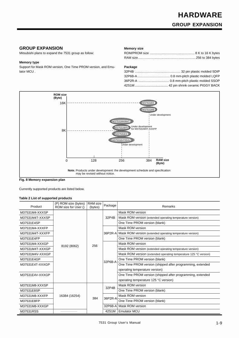
GROUP EXPANSIONMitsubishi plans to expand the 7531 group as follow:
Memory typeSupport for Mask ROM version, One Time PROM version, and Emu-lator MCU .
Memory sizeROM/PROM size .................................................. 8 K to 16 K bytesRAM size ................................................................ 256 to 384 bytes
Package32P4B ................................................... 32 pin plastic molded SDIP32P6B-A .................................... 0.8 mm-pitch plastic molded LQFP36P2R-A .................................. 0.8 mm-pitch plastic molded SSOP42S1M ..................................... 42 pin shrink ceramic PIGGY BACK
Fig. 8 Memory expansion plan
Currently supported products are listed below.
Table 2 List of supported products
Product
M37531M4-XXXSP
M37531M4T-XXXSP
M37531E4SP
M37531M4-XXXFP
M37531M4T-XXXFP
M37531E4FP
M37531M4-XXXGP
M37531M4T-XXXGP
M37531M4V-XXXGP
M37531E4GP
M37531E4T-XXXGP
M37531E4V-XXXGP
M37531M8-XXXSP
M37531E8SP
M37531M8-XXXFP
M37531E8FP
M37531M8-XXXGP
M37531RSS
(P) ROM size (bytes)ROM size for User ()
8192 (8062)
RAM size(bytes)
256
Package
32P4B
36P2R-A
32P6B-A
Remarks
Mask ROM version
Mask ROM version (extended operating temperature version)
One Time PROM version (blank)
Mask ROM version
Mask ROM version (extended operating temperature version)
One Time PROM version (blank)
Mask ROM version
Mask ROM version (extended operating temperature version)
Mask ROM version (extended operating temperature 125 °C version)
One Time PROM version (blank)
One Time PROM version (shipped after programming, extended
operating temperature version)
One Time PROM version (shipped after programming, extended
operating temperature 125 °C version)
Mask ROM version
One Time PROM version (blank)
Mask ROM version
One Time PROM version (blank)
Mask ROM version
Emulator MCU
ROM size(Byte)
Under development
RAM size(Byte)
Note. Products under development: the development schedule and specification may be revised without notice.
128
16K
256 384
8K
0
M37531E8
M37531M4/M4T
M37531E4
Under development for M37531M4T-XXXFP
Under development
M37531M8
M37531E4T/E4V
M37531M4V
16384 (16254)384
32P4B
36P2R-A
42S1M
32P6B-A
GROUP EXPANSION
HARDWARE
7531 Group User’s Manual1-10
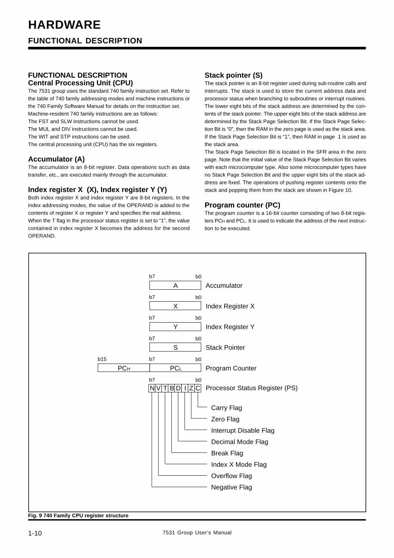
FUNCTIONAL DESCRIPTIONCentral Processing Unit (CPU)The 7531 group uses the standard 740 family instruction set. Refer tothe table of 740 family addressing modes and machine instructions orthe 740 Family Software Manual for details on the instruction set.Machine-resident 740 family instructions are as follows:The FST and SLW instructions cannot be used.The MUL and DIV instructions cannot be used.The WIT and STP instructions can be used.The central processing unit (CPU) has the six registers.
Accumulator (A)The accumulator is an 8-bit register. Data operations such as datatransfer, etc., are executed mainly through the accumulator.
Index register X (X), Index register Y (Y)Both index register X and index register Y are 8-bit registers. In theindex addressing modes, the value of the OPERAND is added to thecontents of register X or register Y and specifies the real address.When the T flag in the processor status register is set to “1”, the valuecontained in index register X becomes the address for the secondOPERAND.
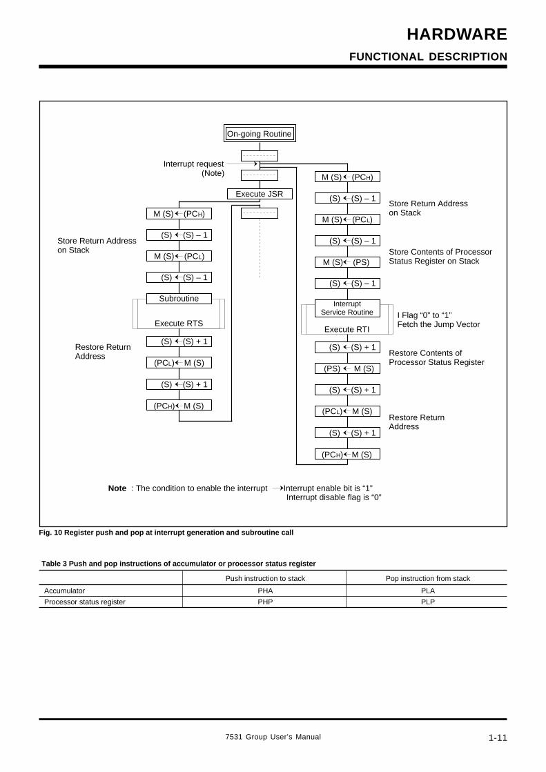
Stack pointer (S)The stack pointer is an 8-bit register used during sub-routine calls andinterrupts. The stack is used to store the current address data andprocessor status when branching to subroutines or interrupt routines.The lower eight bits of the stack address are determined by the con-tents of the stack pointer. The upper eight bits of the stack address aredetermined by the Stack Page Selection Bit. If the Stack Page Selec-tion Bit is “0”, then the RAM in the zero page is used as the stack area.If the Stack Page Selection Bit is “1”, then RAM in page 1 is used asthe stack area.The Stack Page Selection Bit is located in the SFR area in the zeropage. Note that the initial value of the Stack Page Selection Bit varieswith each microcomputer type. Also some microcomputer types haveno Stack Page Selection Bit and the upper eight bits of the stack ad-dress are fixed. The operations of pushing register contents onto thestack and popping them from the stack are shown in Figure 10.
Program counter (PC)The program counter is a 16-bit counter consisting of two 8-bit regis-ters PCH and PCL. It is used to indicate the address of the next instruc-tion to be executed.
Fig. 9 740 Family CPU register structure
b7 b0
X
b7 b0
S
b7 b0
Y
b7 b0
PCL
Processor Status Register (PS)
Carry Flag
b7 b0
b7 b0
A
b15
PCH
Zero Flag
Interrupt Disable Flag
Decimal Mode Flag
Break Flag
Index X Mode Flag
Overflow Flag
Negative Flag
Program Counter
Stack Pointer
Index Register Y
Index Register X
Accumulator
CZIDBTVN
FUNCTIONAL DESCRIPTION
7531 Group User’s Manual 1-11
HARDWARE
Table 3 Push and pop instructions of accumulator or processor status register
Accumulator
Processor status register
Push instruction to stack
PHA
PHP
Pop instruction from stack
PLA
PLP
Fig. 10 Register push and pop at interrupt generation and subroutine call
Execute JSR
On-going Routine
M (S) (PCH)
(S) (S) – 1
M (S) (PCL)
Execute RTS
(PCL) M (S)
(S) (S) – 1
(S) (S) + 1
(S) (S) + 1
(PCH) M (S)
Subroutine
Restore ReturnAddress
Store Return Address on Stack
M (S) (PS)
Execute RTI
(PS) M (S)
(S) (S) – 1
(S) (S) + 1
Interrupt Service Routine
Restore Contents of Processor Status Register
M (S) (PCH)
(S) (S) – 1
M (S) (PCL)
(S) (S) – 1
(PCL) M (S)
(S) (S) + 1
(S) (S) + 1
(PCH) M (S)
Restore ReturnAddress
I Flag “0” to “1” Fetch the Jump Vector
Store Return Address on Stack
Store Contents of Processor Status Register on Stack
Interrupt request (Note)
Note : The condition to enable the interrupt Interrupt enable bit is “1”Interrupt disable flag is “0”
FUNCTIONAL DESCRIPTION
HARDWARE
7531 Group User’s Manual1-12
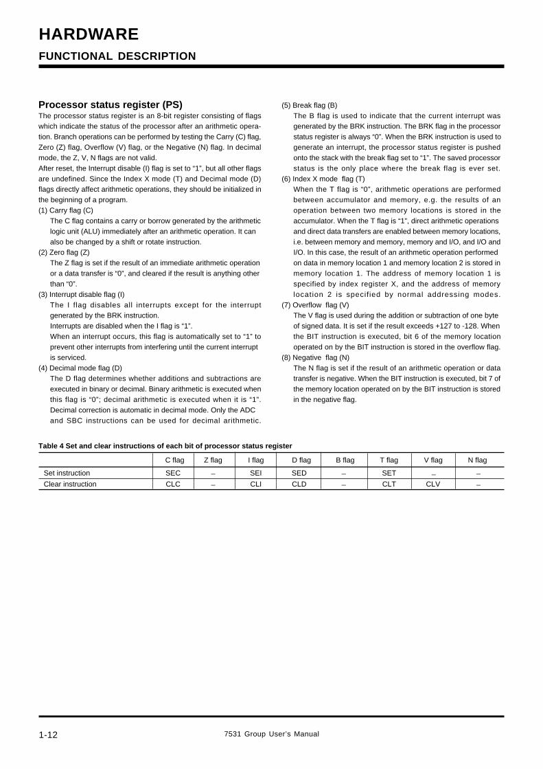
Processor status register (PS)The processor status register is an 8-bit register consisting of flagswhich indicate the status of the processor after an arithmetic opera-tion. Branch operations can be performed by testing the Carry (C) flag,Zero (Z) flag, Overflow (V) flag, or the Negative (N) flag. In decimalmode, the Z, V, N flags are not valid.After reset, the Interrupt disable (I) flag is set to “1”, but all other flagsare undefined. Since the Index X mode (T) and Decimal mode (D)flags directly affect arithmetic operations, they should be initialized inthe beginning of a program.(1) Carry flag (C)
The C flag contains a carry or borrow generated by the arithmeticlogic unit (ALU) immediately after an arithmetic operation. It canalso be changed by a shift or rotate instruction.
(2) Zero flag (Z)The Z flag is set if the result of an immediate arithmetic operationor a data transfer is “0”, and cleared if the result is anything otherthan “0”.
(3) Interrupt disable flag (I)The I flag disables all interrupts except for the interruptgenerated by the BRK instruction.Interrupts are disabled when the I flag is “1”.When an interrupt occurs, this flag is automatically set to “1” toprevent other interrupts from interfering until the current interruptis serviced.
(4) Decimal mode flag (D)The D flag determines whether additions and subtractions areexecuted in binary or decimal. Binary arithmetic is executed whenthis flag is “0”; decimal arithmetic is executed when it is “1”.Decimal correction is automatic in decimal mode. Only the ADCand SBC instructions can be used for decimal arithmetic.
(5) Break flag (B)The B flag is used to indicate that the current interrupt wasgenerated by the BRK instruction. The BRK flag in the processorstatus register is always “0”. When the BRK instruction is used togenerate an interrupt, the processor status register is pushedonto the stack with the break flag set to “1”. The saved processorstatus is the only place where the break flag is ever set.
(6) Index X mode flag (T)When the T flag is “0”, arithmetic operations are performedbetween accumulator and memory, e.g. the results of anoperation between two memory locations is stored in theaccumulator. When the T flag is “1”, direct arithmetic operationsand direct data transfers are enabled between memory locations,i.e. between memory and memory, memory and I/O, and I/O andI/O. In this case, the result of an arithmetic operation performedon data in memory location 1 and memory location 2 is stored inmemory location 1. The address of memory location 1 isspecified by index register X, and the address of memorylocation 2 is specif ied by normal addressing modes.
(7) Overflow flag (V)The V flag is used during the addition or subtraction of one byteof signed data. It is set if the result exceeds +127 to -128. Whenthe BIT instruction is executed, bit 6 of the memory locationoperated on by the BIT instruction is stored in the overflow flag.
(8) Negative flag (N)The N flag is set if the result of an arithmetic operation or datatransfer is negative. When the BIT instruction is executed, bit 7 ofthe memory location operated on by the BIT instruction is storedin the negative flag.
Table 4 Set and clear instructions of each bit of processor status register
Set instruction
Clear instruction
C flag Z flag I flag D flag B flag T flag V flag N flag
SEC
CLC
_
_SEI
CLI
SED
CLD
_
_SET
CLT CLV
_ _
_
FUNCTIONAL DESCRIPTION
7531 Group User’s Manual 1-13
HARDWARE
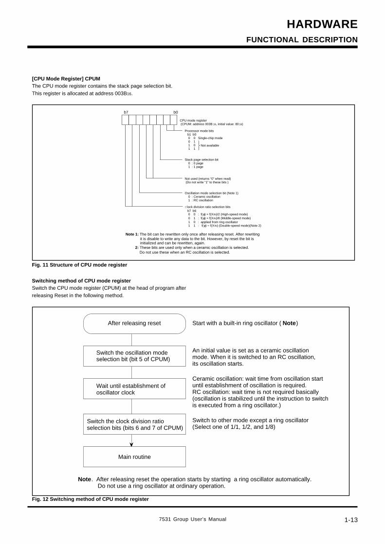
[CPU Mode Register] CPUMThe CPU mode register contains the stack page selection bit.This register is allocated at address 003B16.
Fig. 12 Switching method of CPU mode register
Switching method of CPU mode registerSwitch the CPU mode register (CPUM) at the head of program afterreleasing Reset in the following method.
Fig. 11 Structure of CPU mode register
Oscillation mode selection bit (Note 1) 0 : Ceramic oscillation 1 : RC oscillation
CPU mode register (CPUM: address 003B 16, initial value: 8016)
Stack page selection bit 0 : 0 page 1 : 1 page
C lock division ratio selection bits b7 b6 0 0 : f(φ) = f(XIN)/2 (High-speed mode) 0 1 : f(φ) = f(XIN)/8 (Middle-speed mode) 1 0 : applied from ring oscillator 1 1 : f(φ) = f(XIN) (Double-speed mode)(Note 2)
Not used (returns “0” when read) (Do not write “1” to these bits )
Processor mode bits b1 b0 0 0 Single-chip mode 0 1 1 0 1 1
Not available
b7 b0
2: These bits are used only when a ceramic oscillation is selected.
Note 1: The bit can be rewritten only once after releasing reset. After rewritingit is disable to write any data to the bit. However, by reset the bit is initialized and can be rewritten, again.
Do not use these when an RC oscillation is selected.
Switch the clock division ratio selection bits (bits 6 and 7 of CPUM)
Main routine
Switch to other mode except a ring oscillator(Select one of 1/1, 1/2, and 1/8)
Note. After releasing reset the operation starts by starting a ring oscillator automatically. Do not use a ring oscillator at ordinary operation.
After releasing reset Start with a built-in ring oscillator ( Note)
Switch the oscillation mode selection bit (bit 5 of CPUM)
Wait until establishment ofoscillator clock
An initial value is set as a ceramic oscillation mode. When it is switched to an RC oscillation, its oscillation starts.
Ceramic oscillation: wait time from oscillation start until establishment of oscillation is required.RC oscillation: wait time is not required basically (oscillation is stabilized until the instruction to switch is executed from a ring oscillator.)
FUNCTIONAL DESCRIPTION
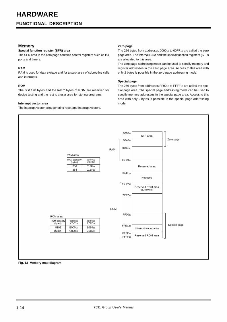
HARDWARE
7531 Group User’s Manual1-14
MemorySpecial function register (SFR) areaThe SFR area in the zero page contains control registers such as I/Oports and timers.
RAMRAM is used for data storage and for a stack area of subroutine callsand interrupts.
ROMThe first 128 bytes and the last 2 bytes of ROM are reserved fordevice testing and the rest is a user area for storing programs.
Interrupt vector areaThe interrupt vector area contains reset and interrupt vectors.
Zero pageThe 256 bytes from addresses 000016 to 00FF16 are called the zeropage area. The internal RAM and the special function registers (SFR)are allocated to this area.The zero page addressing mode can be used to specify memory andregister addresses in the zero page area. Access to this area withonly 2 bytes is possible in the zero page addressing mode.
Special pageThe 256 bytes from addresses FF0016 to FFFF16 are called the spe-cial page area. The special page addressing mode can be used tospecify memory addresses in the special page area. Access to thisarea with only 2 bytes is possible in the special page addressingmode.
Fig. 13 Memory map diagram
010016
000016
004016
044016
FF0016
FFEC16
FFFE16
FFFF16
256384
XXXX16
013F16
01BF16
819216384
E00016
C00016
E08016
C08016
YYYY16
ZZZZ16
RAM
ROM
Reserved area
SFR area
Not used
Interrupt vector area
ROM area
Reserved ROM area(128 bytes)
Zero page
Special page
RAM area
RAM capacity(bytes)
address XXXX16
ROM capacity(bytes)
addressYYYY16
Reserved ROM area
addressZZZZ16
FUNCTIONAL DESCRIPTION
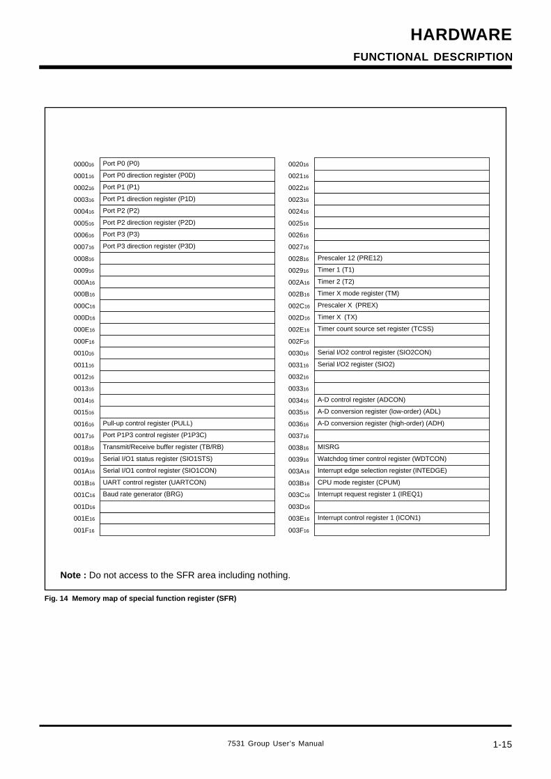
7531 Group User’s Manual 1-15
HARDWARE
Fig. 14 Memory map of special function register (SFR)
Note : Do not access to the SFR area including nothing.
000016
000116
000216
000316
000416
000516
000616
000716
000816
000916
000A16
000B16
000C16
000D16
000E16
000F16
001016
001116
001216
001316
001416
001516
001616
001716
001816
001916
001A16
001B16
001C16
001D16
001E16
001F16
Port P0 (P0)
Port P0 direction register (P0D)
Port P1 (P1)
Port P1 direction register (P1D)
Port P2 (P2)
Port P2 direction register (P2D)
Port P3 (P3)
Port P3 direction register (P3D)
Pull-up control register (PULL)
Transmit/Receive buffer register (TB/RB)
Serial I/O1 status register (SIO1STS)
Serial I/O1 control register (SIO1CON)
UART control register (UARTCON)
Baud rate generator (BRG)
Port P1P3 control register (P1P3C)
002016
002116
002216
002316
002416
002516
002616
002716
002816
002916
002A16
002B16
002C16
002D16
002E16
002F16
003016
003116
003216
003316
003416
003516
003616
003716
003816
003916
003A16
003B16
003C16
003D16
003E16
003F16
Timer count source set register (TCSS)
A-D conversion register (low-order) (ADL)
Prescaler 12 (PRE12)
Timer 1 (T1)
Timer 2 (T2)
Timer X mode register (TM)
Prescaler X (PREX)
Timer X (TX)
Serial I/O2 control register (SIO2CON)
Serial I/O2 register (SIO2)
A-D control register (ADCON)
A-D conversion register (high-order) (ADH)
MISRG
Watchdog timer control register (WDTCON)
Interrupt edge selection register (INTEDGE)
CPU mode register (CPUM)
Interrupt request register 1 (IREQ1)
Interrupt control register 1 (ICON1)
FUNCTIONAL DESCRIPTION
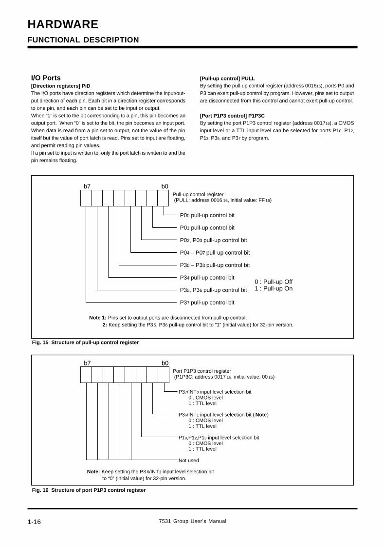
HARDWARE
7531 Group User’s Manual1-16
I/O Ports[Direction registers] PiDThe I/O ports have direction registers which determine the input/out-put direction of each pin. Each bit in a direction register correspondsto one pin, and each pin can be set to be input or output.When “1” is set to the bit corresponding to a pin, this pin becomes anoutput port. When “0” is set to the bit, the pin becomes an input port.When data is read from a pin set to output, not the value of the pinitself but the value of port latch is read. Pins set to input are floating,and permit reading pin values.If a pin set to input is written to, only the port latch is written to and thepin remains floating.
[Pull-up control] PULLBy setting the pull-up control register (address 001616), ports P0 andP3 can exert pull-up control by program. However, pins set to outputare disconnected from this control and cannot exert pull-up control.
[Port P1P3 control] P1P3CBy setting the port P1P3 control register (address 001716), a CMOSinput level or a TTL input level can be selected for ports P10, P12,
P13, P36, and P37 by program.
Fig. 16 Structure of port P1P3 control register
Fig. 15 Structure of pull-up control register
Pull-up control register (PULL: address 0016 16, initial value: FF16)
P00 pull-up control bit
P01 pull-up control bit
P02, P03 pull-up control bit
P04 – P07 pull-up control bit
P30 – P33 pull-up control bit
P34 pull-up control bit
P35, P36 pull-up control bit
P37 pull-up control bit
Note 1: Pins set to output ports are disconnected from pull-up control.
b7 b0
2: Keep setting the P3 5, P36 pull-up control bit to “1” (initial value) for 32-pin version.
0 : Pull-up Off1 : Pull-up On
FUNCTIONAL DESCRIPTION
Port P1P3 control register (P1P3C: address 0017 16, initial value: 0016)
b7 b0
P37/INT0 input level selection bit 0 : CMOS level 1 : TTL level
P36/INT1 input level selection bit ( Note) 0 : CMOS level 1 : TTL level
P10,P12,P13 input level selection bit 0 : CMOS level 1 : TTL level
Not used
Note: Keep setting the P3 6/INT1 input level selection bit to “0” (initial value) for 32-pin version.
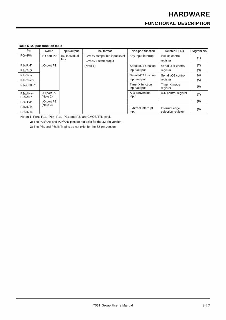
7531 Group User’s Manual 1-17
HARDWARE
Table 5 I/O port function table
Name
I/O port P0
I/O port P1
Pin
P00–P07
P10/RxD
P11/TxD
P12/SCLK
P13/SDATA
P14/CNTR0
P20/AN0–P27/AN7
P30–P35
P36/INT1
P37/INT0
I/O port P2(Note 2)
I/O port P3(Note 3)
Input/output
I/O individualbits
I/O format
•CMOS compatible input level
•CMOS 3-state output
(Note 1)
Non-port function
Key input interrupt
Serial I/O1 functioninput/output
Serial I/O2 functioninput/output
Timer X functioninput/output
A-D conversioninput
External interruptinput
Related SFRs
Pull-up control
register
Serial I/O1 controlregister
Serial I/O2 controlregister
Timer X moderegister
A-D control register
Interrupt edgeselection register
Diagram No.
(1)
(2)
(3)
(4)
(5)
(6)
(7)
(8)
(9)
Notes 1: Ports P10, P12, P13, P36, and P37 are CMOS/TTL level.
2: The P26/AN6 and P27/AN7 pins do not exist for the 32-pin version.
3: The P35 and P36/INT1 pins do not exist for the 32-pin version.
FUNCTIONAL DESCRIPTION
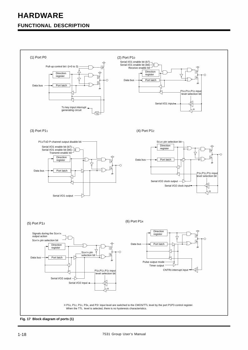
HARDWARE
7531 Group User’s Manual1-18
Fig. 17 Block diagram of ports (1)
(5) Port P13
Data bus
Signals during the SDATAoutput action
Serial I/O2 output
SDATA pin selection bit
P10,P12,P13 input level selection bit
Serial I/O2 input
SDATA pin selection bit
Directionregister
Port latch
(1) Port P0
Data bus
Pull-up control bit i (i=0 to 3)
Data bus
Serial I/O1 enable bit (b7)Serial I/O1 enable bit (b6)
Receive enable bit
Serial I/O1 input
(2) Port P10
Directionregister
Port latch
P10,P12,P13 input level selection bit
Directionregister
Port latch
To key input interrupt generating circuit
(3) Port P11
Data bus
Serial I/O1 output
P11/TxD P-channel output disable bit
Directionregister
Port latch
(4) Port P12
Data bus
Serial I/O2 clock output
SCLK pin selection bit
Serial I/O2 clock input
Directionregister
Port latch
P10,P12,P13 input level selection bit
(6) Port P14
Data bus
Timer outputPulse output mode
CNTR0 interrupt input
Directionregister
Port latch
P10, P12, P13, P36, and P37 input level are switched to the CMOS/TTL level by the port P1P3 control register.
Serial I/O1 enable bit (b7)Serial I/O1 enable bit (b6)
Transmit enable bit
When the TTL level is selected, there is no hysteresis characteristics.
FUNCTIONAL DESCRIPTION
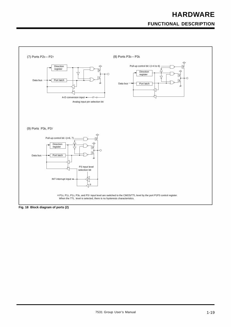
7531 Group User’s Manual 1-19
HARDWARE
Fig. 18 Block diagram of ports (2)
(7) Ports P20 – P27
A-D conversion input
Data bus
Analog input pin selection bit
Directionregister
Port latch
(8) Ports P30 – P35
Data bus
Pull-up control bit i (i=4 to 6)
Direction register
Port latch
Data bus
Pull-up control bit i (i=6, 7)
(9) Ports P36, P37
INT interrupt input
Direction register
Port latch
P3 input level selection bit
P10, P12, P13, P36, and P37 input level are switched to the CMOS/TTL level by the port P1P3 control register.When the TTL level is selected, there is no hysteresis characteristics.
FUNCTIONAL DESCRIPTION
HARDWARE
7531 Group User’s Manual1-20
InterruptsInterrupts occur by 12 different sources : 4 external sources, 7 inter-nal sources and 1 software source.
Interrupt controlAll interrupts except the BRK instruction interrupt have an interruptrequest bit and an interrupt enable bit, and they are controlled by theinterrupt disable flag. When the interrupt enable bit and the interruptrequest bit are set to “1” and the interrupt disable flag is set to “0”, aninterrupt is accepted.The interrupt request bit can be cleared by program but not be set.The interrupt enable bit can be set and cleared by program.It becomes usable by switching CNTR0 and AD conversion interruptsources with bit 7 of the interrupt edge selection register, timer 2 andserial I/O2 interrupt sources with bit 6, timer X and key-on wake-upinterrupt sources with bit 5, and serial I/O1 transmit and INT1 inter-rupt sources with bit 4.The reset and BRK instruction interrupt can never be disabled withany flag or bit. All interrupts except these are disabled when the in-terrupt disable flag is set.When several interrupts occur at the same time, the interrupts arereceived according to priority.
Interrupt operationUpon acceptance of an interrupt the following operations are auto-matically performed:1. The processing being executed is stopped.2. The contents of the program counter and processor status regis-
ter are automatically pushed onto the stack.3. The interrupt disable flag is set and the corresponding interrupt
request bit is cleared.4. Concurrently with the push operation, the interrupt destination
address is read from the vector table into the program counter.
Notes on useWhen the active edge of an external interrupt (INT0, INT1,CNTR0) isset, the interrupt request bit may be set.Therefore, please take following sequence:1. Disable the external interrupt which is selected.2. Change the active edge in interrupt edge selection register. (in
case of CNTR0: Timer X mode register)3. Clear the set interrupt request bit to “0”.4. Enable the external interrupt which is selected.
Table 6 Interrupt vector address and priority
Vector addresses (Note 1)
High-order
FFFD16
FFFB16
FFF916
FFF716
FFF516
FFF316
FFF116
FFEF16
FFED16
Priority
1
2
3
4
5
6
7
8
9
Low-order
FFFC16
FFFA16
FFF816
FFF616
FFF416
FFF216
FFF016
FFEE16
FFEC16
Interrupt request generating conditions
At reset input
At completion of serial I/O1 data receive
At completion of serial I/O1 transmit shift orwhen transmit buffer is empty
At detection of either rising or falling edgeof INT1 input
At detection of either rising or falling edgeof INT0 input
At timer X underflow
At falling of conjunction of input logicallevel for port P0 (at input)
At timer 1 underflow
At timer 2 underflow
At completion of transmit/receive shift
At detection of either rising or falling edgeof CNTR0 input
At completion of A-D conversion
At BRK instruction execution
Remarks
Non-maskable
Valid when serial I/O1 is selected
Valid when serial I/O1 is selected
External interrupt(active edge selectable)
External interrupt(active edge selectable)
External interrupt (valid at falling)
STP release timer underflow
External interrupt (active edgeselectable)
Non-maskable software interrupt
Interrupt source
Reset (Note 2)
Serial I/O1receive
Serial I/O1transmit
INT1 (Note 3)
INT0
Timer X
Key-on wake-up
Timer 1
Timer 2
Serial I/O2
CNTR0
A-D conversion
BRK instruction
Note 1: Vector addressed contain internal jump destination addresses.
2: Reset function in the same way as an interrupt with the highest priority.
3: It is an interrupt which can use only for 36 pin version.
FUNCTIONAL DESCRIPTION
7531 Group User’s Manual 1-21
HARDWARE
Fig. 19 Interrupt control
Fig. 20 Structure of Interrupt-related registers
b7 b0
b7 b0
Interrupt edge selection register
INT0 interrupt edge selection bit 0 : Falling edge active 1 : Rising edge activeINT1 interrupt edge selection bit 0 : Falling edge active 1 : Rising edge activeNot used (returns “0” when read)Serial I/O1 or INT1 interrupt selection bit(Do not write “1” for 32 pin version) 0 : Serial I/O1 1 : INT1Timer X or key-on wake up interrupt selection bit 0 : Timer X 1 : Key-on wake upTimer 2 or serial I/O2 interrupt selection bit 0 : Timer 2 1 : Serial I/O2CNTR0 or AD converter interrupt selection bit 0 : CNTR0 1 : AD converter
(INTEDGE : address 003A16, initial value: 0016)
Interrupt request register 1
Serial I/O1 receive interrupt request bit Serial I/O1 transmit or INT1 interrupt request bitINT0 interrupt request bitTimer X or key-on wake up interrupt request bitTimer 1 interrupt request bitTimer 2 or serial I/O2 interrupt request bitCNTR0 or AD converter interrupt request bitNot used (returns “0” when read)
0 : No interrupt request issued1 : Interrupt request issued
(IREQ1 : address 003C16, initial value: 0016)
b7 b0 Interrupt control register 1
Serial I/O1 receive interrupt enable bit Serial I/O1 transmit or INT1 interrupt enable bitINT0 interrupt enable bitTimer X or key-on wake up interrupt enable bitTimer 1 interrupt enable bitTimer 2 or serial I/O2 interrupt enable bitCNTR0 or AD converter interrupt enable bitNot used (returns “0” when read)(Do not write “1” to this bit)
0 : Interrupts disabled1 : Interrupts enabled
(ICON1 : address 003E16, initial value: 0016)
FUNCTIONAL DESCRIPTION
Interrupt disable flag I
Interrupt request
Interrupt request bit
Interrupt enable bit
BRK instructionReset
HARDWARE
7531 Group User’s Manual1-22
Key Input Interrupt (Key-On Wake-Up)A key-on wake-up interrupt request is generated by applying “L” levelto any pin of port P0 that has been set to input mode.In other words, it is generated when the AND of input level goes from“1” to “0”. An example of using a key input interrupt is shown in Fig-ure 21, where an interrupt request is generated by pressing one ofthe keys provided as an active-low key matrix which uses ports P00
to P03 as input ports.
Fig. 21 Connection example when using key input interrupt and port P0 block diagram
FUNCTIONAL DESCRIPTION
Port PXx“L” level output
PULL registerbit 3 = “0”
Port P07latch
Port P07Direction register = “1”
***
P07 output
Key input interrupt request
Port P0Input read circuit
* P-channel transistor for pull-up** CMOS output buffer
PULL registerbit 3 = “0”
Port P06 latch
Port P06Direction register = “1”
***
P06 output
PULL registerbit 3 = “0”
Port P05 latch
Port P05Direction register = “1”
***
P05 output
PULL registerbit 3 = “0”
Port P04 latch
Port P04Direction register = “1”
***
P04 output
PULL registerbit 2 = “1”
Port P03 latch
Port P03Direction register = “0”
***
P03 input
PULL registerbit 2 = “1”
Port P02 latch
Port P02Direction register = “0”
***
P02 input
PULL registerbit 1 = “1”
Port P01 latch
Port P01Direction register = “0”
***
P01 input
PULL registerbit 0 = “1”
Port P00 latch
Port P00Direction register = “0”
***
P00 input
Falling edge detection
Falling edge detection
Falling edge detection
Falling edge detection
Falling edge detection
Falling edge detection
Falling edge detection
Falling edge detection
7531 Group User’s Manual 1-23
HARDWARE
TimersThe 7531 Group has 3 timers: timer X, timer 1 and timer 2.The division ratio of every timer and prescaler is 1/(n+1) providedthat the value of the timer latch or prescaler is n.All the timers are down count timers. When a timer reaches “0”, anunderflow occurs at the next count pulse, and the corresponding timerlatch is reloaded into the timer. When a timer underflows, the inter-rupt request bit corresponding to each timer is set to “1”.
Timer 1, Timer 2Prescaler 12 always counts f(XIN)/16. Timer 1 and timer 2 alwayscount the prescaler output and periodically sets the interrupt requestbit.
Timer XTimer X can be selected in one of 4 operating modes by setting thetimer X mode register.
• Timer ModeThe timer counts the signal selected by the timer X count sourceselection bit.
• Pulse Output ModeThe timer counts the signal selected by the timer X count sourceselection bit, and outputs a signal whose polarity is inverted eachtime the timer value reaches “0”, from the CNTR0 pin.When the CNTR0 active edge switch bit is “0”, the output of theCNTR0 pin is started with an “H” output.At “1”, this output is started with an “L” output. When using a timer inthis mode, set the port P14 direction register to output mode.
• Event Counter ModeThe operation in the event counter mode is the same as that in thetimer mode except that the timer counts the input signal from theCNTR0 pin.When the CNTR0 active edge switch bit is “0”, the timer countsthe rising edge of the CNTR0 pin. When this bit is “1”, the timercounts the falling edge of the CNTR0 pin.
• Pulse Width Measurement ModeWhen the CNTR0 active edge switch bit is “0”, the timer counts thesignal selected by the timer X count source selection bit while theCNTR0 pin is “H”. When this bit is “1”, the timer counts the signalwhile the CNTR0 pin is “L”.In any mode, the timer count can be stopped by setting the timer Xcount stop bit to “1”. Each time the timer overflows, the interruptrequest bit is set.
Fig. 22 Structure of timer X mode register
Fig. 23 Timer count source setting register
Timer X mode register(TM : address 002B16, initial value: 0016)
CNTR0 active edge switch bit 0 : Interrupt at falling edge Count at rising edge (in event counter mode) 1 : Interrupt at rising edge Count at falling edge (in event counter mode)
Timer X operating mode bits b1 b0 0 0 : Timer mode 0 1 : Pulse output mode 1 0 : Event counter mode 1 1 : Pulse width measurement mode
Not used (return “0” when read)
Timer X count stop bit 0 : Count start 1 : Count stop
b7 b0
Timer count source set register(TCSS : address 002E16, initial value: 0016)
b7 b0
Timer X count source selection bit (Note) 0 : f(XIN)/16 1 : f(XIN)/2
Not used (return “0” when read)
Note : To switch the timer X count source selection bit , stop the timer X count operation.
FUNCTIONAL DESCRIPTION
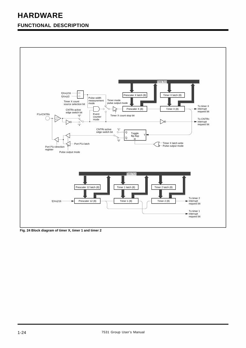
HARDWARE
7531 Group User’s Manual1-24
Fig. 24 Block diagram of timer X, timer 1 and timer 2
Timer modepulse output mode
Q
R
To timer X interrupt request bit
f(XIN)/16Timer X latch (8)
Timer X (8)
Prescaler X latch (8)
Prescaler X (8)
Pulse widthmeasurementmode
f(XIN)/2
Timer X countsource selection bit
Event countermode
Timer X count stop bit
Port P14 direction register
Q“0”
“1”CNTR0 activeedge switch bit
Port P14 latch
Pulse output mode
“1”
“0”
CNTR0 activeedge switch bit
P14/CNTR0
Toggleflip-flop
Timer X latch writePulse output mode
T
To CNTR0
interrupt request bit
Data bus
To timer 1
interrupt request bit
To timer 2 interrupt request bit
Data bus
Prescaler 12 (8)f(XIN)/16 Timer 1 (8) Timer 2 (8)
Timer 2 latch (8)Timer 1 latch (8)Prescaler 12 latch (8)
FUNCTIONAL DESCRIPTION
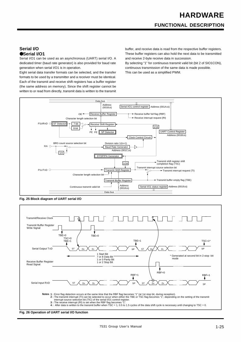
7531 Group User’s Manual 1-25
HARDWARE
Fig. 25 Block diagram of UART serial I/O
Fig. 26 Operation of UART serial I/O function
Serial I/OSerial I/O1Serial I/O1 can be used as an asynchronous (UART) serial I/O. Adedicated timer (baud rate generator) is also provided for baud rategeneration when serial I/O1 is in operation.Eight serial data transfer formats can be selected, and the transferformats to be used by a transmitter and a receiver must be identical.Each of the transmit and receive shift registers has a buffer register(the same address on memory). Since the shift register cannot bewritten to or read from directly, transmit data is written to the transmit
buffer, and receive data is read from the respective buffer registers.These buffer registers can also hold the next data to be transmittedand receive 2-byte receive data in succession.By selecting “1” for continuous transmit valid bit (bit 2 of SIO1CON),continuous transmission of the same data is made possible.This can be used as a simplified PWM.
TSC=0TBE=1
RBF=0
TBE=0 TBE=0
RBF=1 RBF=1
STD0 D1 SP D0 D1STSP
TBE=1 TSC=1*
STD0 D1 SP D0 D1ST SP
1 : Error flag detection occurs at the same time that the RBF flag becomes “1” (at 1st stop bit, during reception).2 : The transmit interrupt (TI) can be selected to occur when either the TBE or TSC flag becomes “1”, depending on the setting of the transmit interrupt source selection bit (TIC) of the serial I/O1 control register.3 : The receive interrupt (RI) is set when the RBF flag becomes “1”.4 : After data is written to the transmit buffer when TSC = 1, 0.5 to 1.5 cycles of the data shift cycle is necessary until changing to TSC = 0.
Notes
Transmit/Receive Clock
Transmit Buffer Register Write Signal
Serial Output TXD
Receive Buffer Register Read Signal
Serial Input RXD
* Generated at second bit in 2-stop -bit mode
1 Start Bit7 or 8 Data Bit1 or 0 Parity Bit1 or 2 Stop Bit
OE
PE FE
1/16
XIN
1/4
1/16
Data bus
Receive Buffer Register
Address(001816)
Receive Shift Register
Receive buffer full flag (RBF)
Receive interrupt request (RI)
ST Detector
SP Detector UART Control Register
Address (001A16)
Character length selection bit
7-bit
8-bit
Address (001B16)Clock Control Circuit
Baud Rate Generator
Division ratio 1/(n+1)
Address (001C16)
BRG count source selection bit
Transmit Buffer Register
Data bus
Transmit Shift Register
Address(001816)
Transmit shift register shift completion flag (TSC)
Transmit buffer empty flag (TBE)
Transmit interrupt request (TI)
Address (001916)
Character length selection bit
Transmit interrupt source selection bit
Continuous transmit valid bit
Serial I/O1 control register
P10/RXD
P11/TXD
Serial I/O1 status register
ST/SP/PA Generator
FUNCTIONAL DESCRIPTION
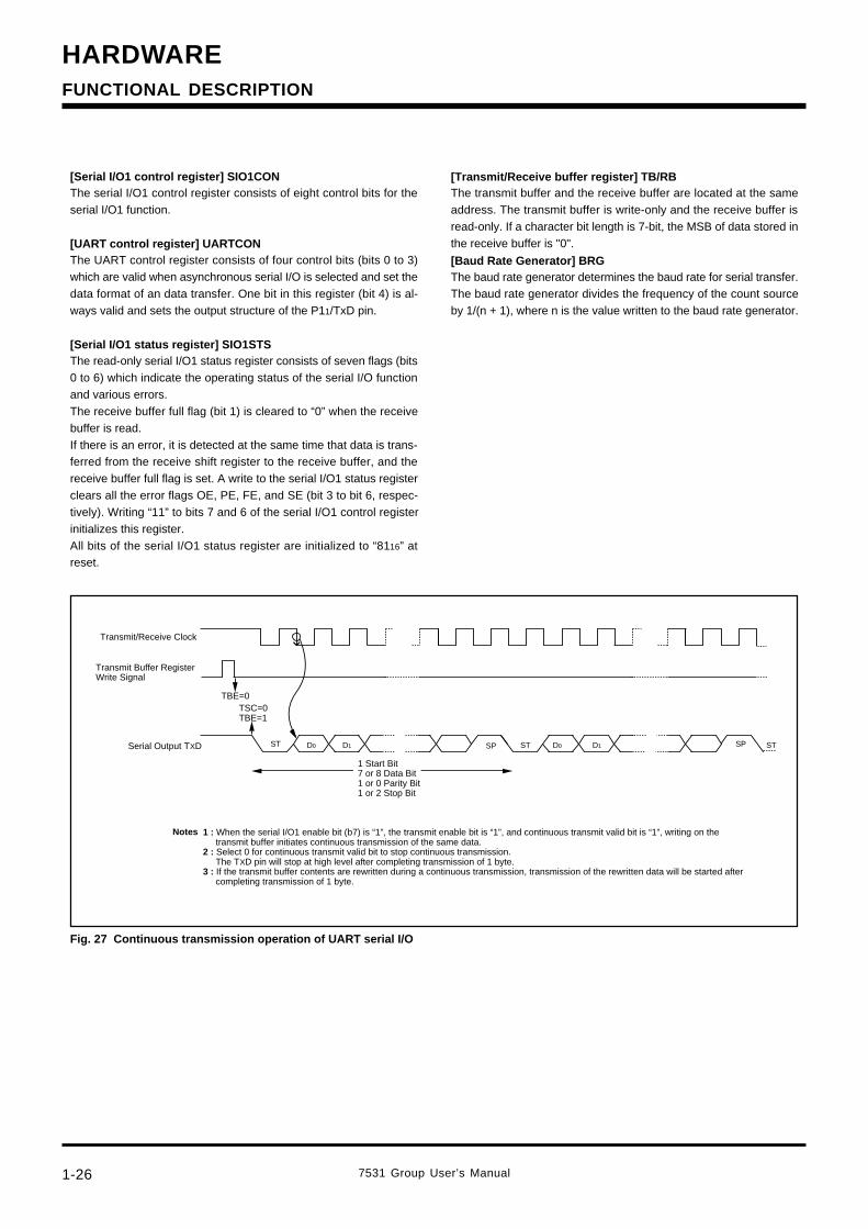
HARDWARE
7531 Group User’s Manual1-26
Fig. 27 Continuous transmission operation of UART serial I/O
[Serial I/O1 control register] SIO1CONThe serial I/O1 control register consists of eight control bits for theserial I/O1 function.
[UART control register] UARTCONThe UART control register consists of four control bits (bits 0 to 3)which are valid when asynchronous serial I/O is selected and set thedata format of an data transfer. One bit in this register (bit 4) is al-ways valid and sets the output structure of the P11/TxD pin.
[Serial I/O1 status register] SIO1STSThe read-only serial I/O1 status register consists of seven flags (bits0 to 6) which indicate the operating status of the serial I/O functionand various errors.The receive buffer full flag (bit 1) is cleared to “0” when the receivebuffer is read.If there is an error, it is detected at the same time that data is trans-ferred from the receive shift register to the receive buffer, and thereceive buffer full flag is set. A write to the serial I/O1 status registerclears all the error flags OE, PE, FE, and SE (bit 3 to bit 6, respec-tively). Writing “11” to bits 7 and 6 of the serial I/O1 control registerinitializes this register.All bits of the serial I/O1 status register are initialized to “8116” atreset.
[Transmit/Receive buffer register] TB/RBThe transmit buffer and the receive buffer are located at the sameaddress. The transmit buffer is write-only and the receive buffer isread-only. If a character bit length is 7-bit, the MSB of data stored inthe receive buffer is "0".
[Baud Rate Generator] BRGThe baud rate generator determines the baud rate for serial transfer.The baud rate generator divides the frequency of the count sourceby 1/(n + 1), where n is the value written to the baud rate generator.
TSC=0TBE=1
TBE=0
STD0 D1 SP D0 D1ST SP ST
1 : When the serial I/O1 enable bit (b7) is “1”, the transmit enable bit is “1”, and continuous transmit valid bit is “1”, writing on the transmit buffer initiates continuous transmission of the same data.2 : Select 0 for continuous transmit valid bit to stop continuous transmission. The TXD pin will stop at high level after completing transmission of 1 byte.3 : If the transmit buffer contents are rewritten during a continuous transmission, transmission of the rewritten data will be started after completing transmission of 1 byte.
Notes
1 Start Bit7 or 8 Data Bit1 or 0 Parity Bit1 or 2 Stop Bit
Transmit/Receive Clock
Transmit Buffer Register Write Signal
Serial Output TXD
FUNCTIONAL DESCRIPTION
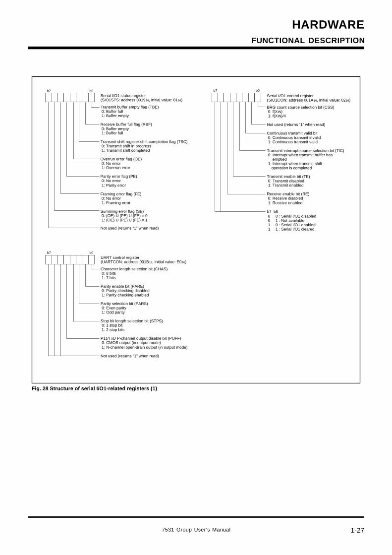
7531 Group User’s Manual 1-27
HARDWARE
Fig. 28 Structure of serial I/O1-related registers (1)
b7 b0Serial I/O1 status register(SIO1STS: address 001916, initial value: 8116)
Transmit buffer empty flag (TBE) 0: Buffer full 1: Buffer empty
Receive buffer full flag (RBF) 0: Buffer empty 1: Buffer full
Transmit shift register shift completion flag (TSC) 0: Transmit shift in progress 1: Transmit shift completed
Overrun error flag (OE) 0: No error 1: Overrun error
Parity error flag (PE) 0: No error 1: Parity error
Framing error flag (FE) 0: No error 1: Framing error
Summing error flag (SE) 0: (OE) U (PE) U (FE) = 0 1: (OE) U (PE) U (FE) = 1
Not used (returns “1” when read)
UART control register(UARTCON: address 001B16, initial value: E016)
Character length selection bit (CHAS) 0: 8 bits 1: 7 bits
Parity enable bit (PARE) 0: Parity checking disabled 1: Parity checking enabled
Parity selection bit (PARS) 0: Even parity 1: Odd parity
Stop bit length selection bit (STPS) 0: 1 stop bit 1: 2 stop bits
P11/TxD P-channel output disable bit (POFF) 0: CMOS output (in output mode) 1: N-channel open-drain output (in output mode)
Not used (returns “1” when read)
b7 b0
b7 b0
Serial I/O1 control register(SIO1CON: address 001A16, initial value: 0216)
BRG count source selection bit (CSS) 0: f(XIN) 1: f(XIN)/4
Not used (returns “1” when read)
Continuous transmit valid bit 0: Continuous transmit invalid 1: Continuous transmit valid
Transmit interrupt source selection bit (TIC) 0: Interrupt when transmit buffer has emptied 1: Interrupt when transmit shift operation is completed
Transmit enable bit (TE) 0: Transmit disabled 1: Transmit enabled
Receive enable bit (RE) 0: Receive disabled 1: Receive enabled
b7 b6 0 0 : Serial I/O1 disabled 0 1 : Not available 1 0 : Serial I/O1 enabled 1 1 : Serial I/O1 cleared
FUNCTIONAL DESCRIPTION
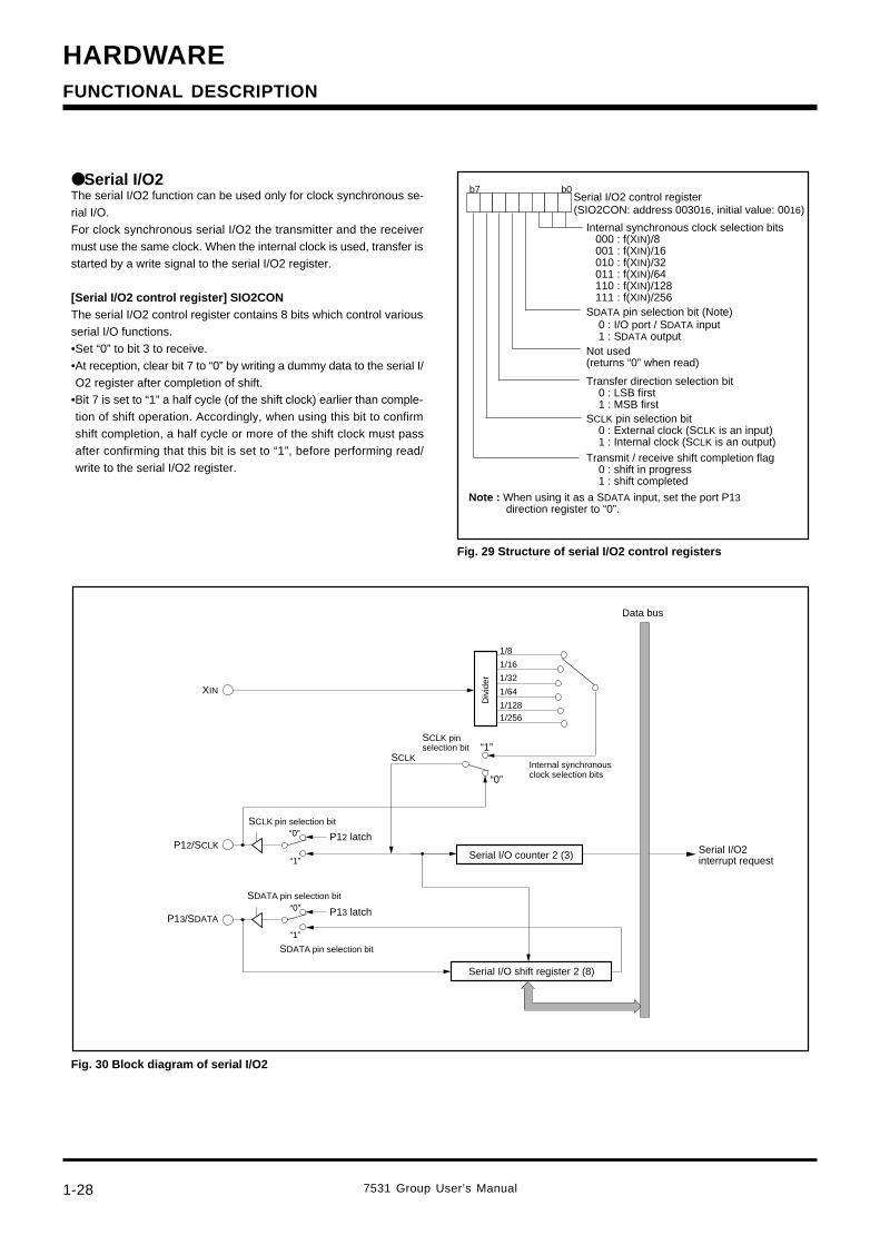
HARDWARE
7531 Group User’s Manual1-28
Serial I/O2The serial I/O2 function can be used only for clock synchronous se-rial I/O.For clock synchronous serial I/O2 the transmitter and the receivermust use the same clock. When the internal clock is used, transfer isstarted by a write signal to the serial I/O2 register.
[Serial I/O2 control register] SIO2CONThe serial I/O2 control register contains 8 bits which control variousserial I/O functions.•Set “0” to bit 3 to receive.•At reception, clear bit 7 to “0” by writing a dummy data to the serial I/O2 register after completion of shift.
•Bit 7 is set to “1” a half cycle (of the shift clock) earlier than comple-tion of shift operation. Accordingly, when using this bit to confirmshift completion, a half cycle or more of the shift clock must passafter confirming that this bit is set to “1”, before performing read/write to the serial I/O2 register.
Fig. 29 Structure of serial I/O2 control registers
Fig. 30 Block diagram of serial I/O2
Internal synchronous clock selection bits 000 : f(XIN)/8 001 : f(XIN)/16 010 : f(XIN)/32 011 : f(XIN)/64 110 : f(XIN)/128 111 : f(XIN)/256
b7 b0
Not used(returns “0” when read)
Transfer direction selection bit 0 : LSB first 1 : MSB firstSCLK pin selection bit 0 : External clock (SCLK is an input) 1 : Internal clock (SCLK is an output)Transmit / receive shift completion flag 0 : shift in progress 1 : shift completed
Note : When using it as a SDATA input, set the port P13 direction register to “0”.
Serial I/O2 control register(SIO2CON: address 003016, initial value: 0016)
SDATA pin selection bit (Note) 0 : I/O port / SDATA input 1 : SDATA output
“1”
“0”
“0”
“1”
“0”
“1”
1/8
1/16
1/32
1/64
1/1281/256
XIN
Data bus
Serial I/O2interrupt request
SDATA pin selection bit
Serial I/O counter 2 (3)
Serial I/O shift register 2 (8)
SCLK pin selection bit
Internal synchronous clock selection bits
Div
ider
P12/SCLK
P13/SDATA
P12 latch
SCLK pinselection bit
SCLK
P13 latch
SDATA pin selection bit
FUNCTIONAL DESCRIPTION
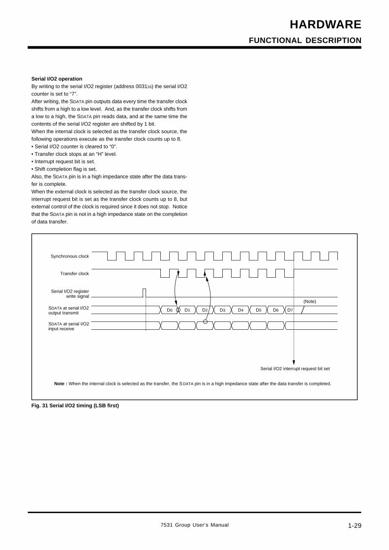
7531 Group User’s Manual 1-29
HARDWARE
Serial I/O2 operationBy writing to the serial I/O2 register (address 003116) the serial I/O2counter is set to “7”.After writing, the SDATA pin outputs data every time the transfer clockshifts from a high to a low level. And, as the transfer clock shifts froma low to a high, the SDATA pin reads data, and at the same time thecontents of the serial I/O2 register are shifted by 1 bit.When the internal clock is selected as the transfer clock source, thefollowing operations execute as the transfer clock counts up to 8.• Serial I/O2 counter is cleared to “0”.• Transfer clock stops at an “H” level.• Interrupt request bit is set.• Shift completion flag is set.Also, the SDATA pin is in a high impedance state after the data trans-fer is complete.When the external clock is selected as the transfer clock source, theinterrupt request bit is set as the transfer clock counts up to 8, butexternal control of the clock is required since it does not stop. Noticethat the SDATA pin is not in a high impedance state on the completionof data transfer.
Fig. 31 Serial I/O2 timing (LSB first)
D0
: When the internal clock is selected as the transfer, the S DATA pin is in a high impedance state after the data transfer is completed.Note
Synchronous clock
Serial I/O2 register write signal
Transfer clock
(Note)
SDATA at serial I/O2 input receive
SDATA at serial I/O2 output transmit
Serial I/O2 interrupt request bit set
D1 D2 D3 D4 D5 D6 D7
FUNCTIONAL DESCRIPTION
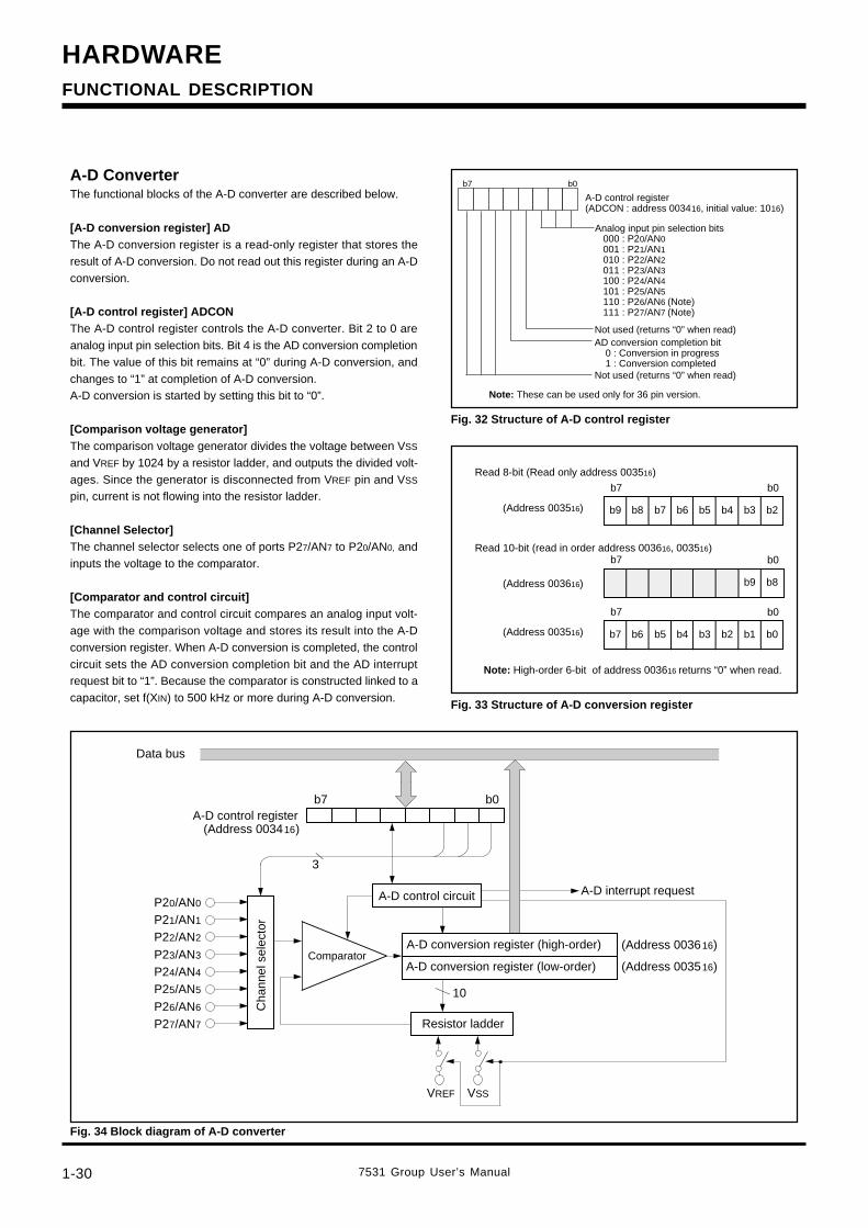
HARDWARE
7531 Group User’s Manual1-30
A-D ConverterThe functional blocks of the A-D converter are described below.
[A-D conversion register] ADThe A-D conversion register is a read-only register that stores theresult of A-D conversion. Do not read out this register during an A-Dconversion.
[A-D control register] ADCONThe A-D control register controls the A-D converter. Bit 2 to 0 areanalog input pin selection bits. Bit 4 is the AD conversion completionbit. The value of this bit remains at “0” during A-D conversion, andchanges to “1” at completion of A-D conversion.A-D conversion is started by setting this bit to “0”.
[Comparison voltage generator]The comparison voltage generator divides the voltage between VSS
and VREF by 1024 by a resistor ladder, and outputs the divided volt-ages. Since the generator is disconnected from VREF pin and VSS
pin, current is not flowing into the resistor ladder.
[Channel Selector]The channel selector selects one of ports P27/AN7 to P20/AN0, andinputs the voltage to the comparator.
[Comparator and control circuit]The comparator and control circuit compares an analog input volt-age with the comparison voltage and stores its result into the A-Dconversion register. When A-D conversion is completed, the controlcircuit sets the AD conversion completion bit and the AD interruptrequest bit to “1”. Because the comparator is constructed linked to acapacitor, set f(XIN) to 500 kHz or more during A-D conversion.
Fig. 32 Structure of A-D control register
Fig. 33 Structure of A-D conversion register
Fig. 34 Block diagram of A-D converter
A-D control register(ADCON : address 003416, initial value: 1016)
Not used (returns “0” when read)
Not used (returns “0” when read)
AD conversion completion bit 0 : Conversion in progress 1 : Conversion completed
b7 b0
Analog input pin selection bits 000 : P20/AN0 001 : P21/AN1 010 : P22/AN2 011 : P23/AN3 100 : P24/AN4 101 : P25/AN5 110 : P26/AN6 (Note) 111 : P27/AN7 (Note)
Note: These can be used only for 36 pin version.
Read 8-bit (Read only address 003516)
b7 b0
b9 b8 b7 b6 b5 b4 b3 b2(Address 003516)
Read 10-bit (read in order address 003616, 003516) b7 b0
b9 b8(Address 003616)
b7 b0
b7 b6 b5 b4 b3 b2 b1 b0(Address 003516)
Note: High-order 6-bit of address 003616 returns “0” when read.
A-D control register(Address 003416)
Cha
nnel
sel
ecto
r
A-D control circuit
Resistor ladder
VREF VSS
Comparator
A-D interrupt request
b7 b0
Data bus
3
10
P20/AN0
P21/AN1
P22/AN2
P23/AN3
P24/AN4
P25/AN5
P26/AN6
P27/AN7
A-D conversion register (low-order)
(Address 003616)
(Address 003516)
A-D conversion register (high-order)
FUNCTIONAL DESCRIPTION
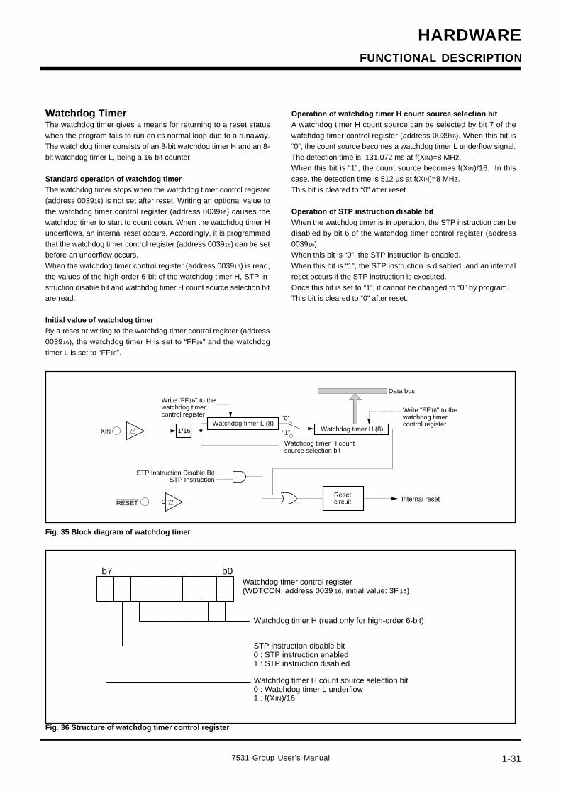
7531 Group User’s Manual 1-31
HARDWARE
Watchdog TimerThe watchdog timer gives a means for returning to a reset statuswhen the program fails to run on its normal loop due to a runaway.The watchdog timer consists of an 8-bit watchdog timer H and an 8-bit watchdog timer L, being a 16-bit counter.
Standard operation of watchdog timerThe watchdog timer stops when the watchdog timer control register(address 003916) is not set after reset. Writing an optional value tothe watchdog timer control register (address 003916) causes thewatchdog timer to start to count down. When the watchdog timer Hunderflows, an internal reset occurs. Accordingly, it is programmedthat the watchdog timer control register (address 003916) can be setbefore an underflow occurs.When the watchdog timer control register (address 003916) is read,the values of the high-order 6-bit of the watchdog timer H, STP in-struction disable bit and watchdog timer H count source selection bitare read.
Initial value of watchdog timerBy a reset or writing to the watchdog timer control register (address003916), the watchdog timer H is set to “FF16” and the watchdogtimer L is set to “FF16”.
Operation of watchdog timer H count source selection bitA watchdog timer H count source can be selected by bit 7 of thewatchdog timer control register (address 003916). When this bit is“0”, the count source becomes a watchdog timer L underflow signal.The detection time is 131.072 ms at f(XIN)=8 MHz.When this bit is “1”, the count source becomes f(XIN)/16. In thiscase, the detection time is 512 µs at f(XIN)=8 MHz.This bit is cleared to “0” after reset.
Operation of STP instruction disable bitWhen the watchdog timer is in operation, the STP instruction can bedisabled by bit 6 of the watchdog timer control register (address003916).When this bit is “0”, the STP instruction is enabled.When this bit is “1”, the STP instruction is disabled, and an internalreset occurs if the STP instruction is executed.Once this bit is set to “1”, it cannot be changed to “0” by program.This bit is cleared to “0” after reset.
Fig. 35 Block diagram of watchdog timer
Fig. 36 Structure of watchdog timer control register
XIN
Data bus
“0”
“1”1/16
Watchdog timer H count source selection bit
Resetcircuit
STP Instruction Disable Bit
Watchdog timer H (8)
Write "FF16" to the watchdog timer control register
Internal resetRESET
Watchdog timer L (8)
STP Instruction
Write “FF16” to the watchdog timer control register
FUNCTIONAL DESCRIPTION
Watchdog timer control register(WDTCON: address 0039 16, initial value: 3F 16)
Watchdog timer H (read only for high-order 6-bit)
STP instruction disable bit0 : STP instruction enabled1 : STP instruction disabled
Watchdog timer H count source selection bit0 : Watchdog timer L underflow1 : f(XIN)/16
b7 b0
HARDWARE
7531 Group User’s Manual1-32
Reset Circuit______
The microcomputer is put into a reset status by holding the RESETpin at the “L” level for 2 µs or more when the power source voltage is2.2 to 5.5 V and XIN is in stable oscillation.
______
After that, this reset status is released by returning the RESET pin tothe “H” level. The program starts from the address having the con-tents of address FFFD16 as high-order address and the contents ofaddress FFFC16 as low-order address.In the case of f(φ) ≤ 4 MHz, the reset input voltage must be 0.8 V orless when the power source voltage passes 4.0 V.In the case of f(φ) ≤ 2 MHz, the reset input voltage must be 0.48 V orless when the power source voltage passes 2.4 V.In the case of f(φ) ≤ 1 MHz, the reset input voltage must be 0.44 V orless when the power source voltage passes 2.2 V.
Fig. 37 Example of reset circuit
Fig. 38 Timing diagram at reset
(Note)
0.2 VCC
0 V
0 V
Poweron
VCCRESET
VCCRESET
Power source voltage detection circuit
Power source voltage
Reset input voltage
Note : Reset release voltage Vcc = 2.2 V
Data
Address
8-13 clock cycles
Reset address from the vector table
1 : A built-in ring oscillator applies about 250 kHz frequency as clock φ at average of Vcc = 5 V.2 : The mark “?” means that the address is changeable depending on the previous state.3 : These are all internal signals except RESET.
Notes
φ
RESET
RESETOUT
SYNC
? ? FFFC FFFD ADH,ADL? ? ?
? ? ADL ADH? ? ?
Clock from built-in ring oscillator
FUNCTIONAL DESCRIPTION
7531 Group User’s Manual 1-33
HARDWARE
Fig. 39 Internal status of microcomputer at reset
Prescaler 12
Timer 1
Timer 2
Timer X mode register
Prescaler X
Timer X
Timer count source set register
Serial I/O2 control register
A-D control register
MISRG
Watchdog timer control register
Interrupt edge selection register
CPU mode register
Interrupt request register 1
Interrupt control register 1
Processor status register
Program counter
(10)
(11)
(12)
(13)
(14)
(15)
(16)
(17)
(18)
(19)
(20)
(21)
(22)
(23)
(24)
(25)
(26)
Contents of address FFFC16
(PCH)
(PCL)
FF16
0116
0016
0016
FF16
FF16
0016
0016
1016
0016
002816
002916
002A16
002B16
002C16
002D16
002E16
003016
003416
003816
003916
003A16
003B16
003C16
003E16
(PS)
Note X : Undefined
Contents of address FFFD16
0 0 1 1 1 1 1 1
0016
0016
0016
1 0 0 0 0 0 0 0
X X X X X 1 X X
Port P0 direction register
Port P1 direction register
Port P2 direction register
Port P3 direction register
Pull-up control register
(1)
(2)
(3)
(4)
(5)
Register contents
0016
0016
FF16
0016000116
000316
000516
000716
001616
Serial I/O1 control register
UART control register
(8)
(9)
Serial I/O1 status register(7)
001A16
001B16
0216
1 1 1 0 0 0 0 0
001916 1 0 0 0 0 0 0 1
X X X 0 0 0 0 0
Address
Port P1P3 control register (6) 001716 0016
FUNCTIONAL DESCRIPTION
HARDWARE
7531 Group User’s Manual1-34
Clock Generating CircuitAn oscillation circuit can be formed by connecting a resonator be-tween XIN and XOUT, and an RC oscillation circuit can be formed byconnecting a resistor and a capacitor.Use the circuit constants in accordance with the resonatormanufacturer's recommended values. No external resistor is neededbetween XIN and XOUT since a feed-back resistor exists on-chip.Set the constants of the resistor and capacitor when an RC oscillatoris used, so that a frequency variation due to LSI variation and resis-tor and capacitor variations may not exceed the standard input fre-quency.
Oscillation control• Stop mode
When the STP instruction is executed, the internal clock f stops atan “H” level and the XIN oscillator stops. At this time, timer 1 is setto “0116” and prescaler 12 is set to “FF16” when the oscillation sta-bilization time set bit after release of the STP instruction is “0”. Onthe other hand, timer 1 and prescaler 12 are not set when theabove bit is “1”. Accordingly, set the wait time fit for the oscillationstabilization time of the oscillator to be used. f(XIN)/16 is forciblyconnected to the input of prescaler 12. When an external interruptis accepted, oscillation is restarted but the internal clock f remainsat “H” until timer 1 underflows. As soon as timer 1 underflows, theinternal clock f is supplied. This is because when a ceramic oscilla-tor is used, some time is required until a start of oscillation. In caseoscillation is restarted by reset, no wait time is generated. So applyan “L” level to the RESET pin while oscillation becomes stable.
• Wait mode
If the WIT instruction is executed, the internal clock f stops at an “H”level, but the oscillator does not stop. The internal clock restarts ifa reset occurs or when an interrupt is received. Since the oscillatordoes not stop, normal operation can be started immediately afterthe clock is restarted. To ensure that interrupts will be received torelease the STP or WIT state, interrupt enable bits must be set to“1” before the STP or WIT instruction is executed.When the STP status is released, prescaler 12 and timer 1 will startcounting clock which is XIN divided by 16, so set the timer 1 inter-rupt enable bit to “0” before the STP instruction is executed.
NoteFor use with the oscillation stabilization set bit after release of theSTP instruction set to “1”, set values in timer 1 and prescaler12 after fully appreciating the oscillation stabilization time of theoscillator to be used.
Switch of ceramic and RC oscillationsAfter releasing reset the operation starts by starting a built-in ringoscillator. Then, a ceramic oscillation or an RC oscillation is selectedby setting bit 5 of the CPU mode register.The bit 5 can be rewritten only once after releasing reset. However,after rewriting it is disable to write any value to the bit.
Double-speed modeWhen a ceramic oscillation is selected, a double-speed mode can beused. Do not use it when an RC oscillation is selected.
FUNCTIONAL DESCRIPTION
7531 Group User’s Manual 1-35
HARDWARE
Fig. 40 External circuit of ceramic resonator
Fig. 41 External circuit of RC oscillation
Fig. 43 Structure of MISRG
Fig. 42 External clock input circuit
XIN
COUTCIN
XOUT
XIN XOUT
C
R
XIN XOUT
External oscillation circuit
VCC
VSS
Open
MISRG(address 003816, initial value: 0016)
b7 b0
Oscillation stabilization time set bit after release of the STP instruction 0: Set “0116” in timer1, and “FF16” in prescaler 12 automatically 1: Not set automatically
Reserved bits (return “0” when read)(Do not write “1” to these bits)
Not used (return “0” when read)
FUNCTIONAL DESCRIPTION
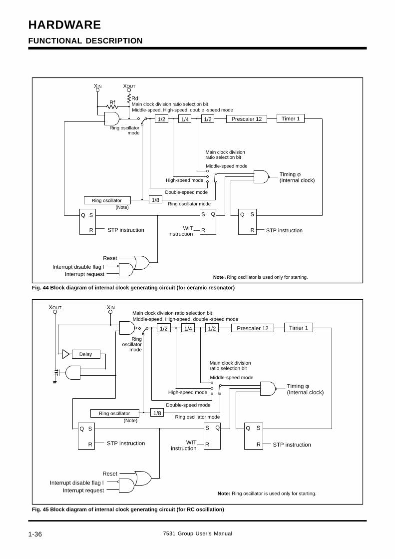
HARDWARE
7531 Group User’s Manual1-36
Fig. 44 Block diagram of internal clock generating circuit (for ceramic resonator)
Fig. 45 Block diagram of internal clock generating circuit (for RC oscillation)
S
R
Q S
R
Q
1/2
Rd
R
SQ
Rf
1/4 1/2
WIT instruction
STP instruction
Timing φ (Internal clock)
STP instruction
Interrupt request
Reset
Interrupt disable flag l
High-speed mode
Middle-speed mode
Prescaler 12 Timer 1
Main clock divisionratio selection bit
Double-speed mode
Ring oscillator modeRing oscillator
(Note)
Note: Ring oscillator is used only for starting.
XOUTXIN
1/8
Middle-speed, High-speed, double -speed modeMain clock division ratio selection bit
Ring oscillator mode
S
R
Q S
R
Q
1/2
R
SQ
1/4 1/2
WIT instruction
STP instruction
Timing φ (Internal clock)
STP instruction
Interrupt request
Reset
Interrupt disable flag l
High-speed mode
Middle-speed mode
Prescaler 12 Timer 1
Main clock divisionratio selection bit
Double-speed mode
Ring oscillator modeRing oscillator
(Note)
Note: Ring oscillator is used only for starting.
XOUT XIN
Delay
1/8
Middle-speed, High-speed, double -speed modeMain clock division ratio selection bit
Ring oscillator
mode
FUNCTIONAL DESCRIPTION
7531 Group User’s Manual 1-37
HARDWARE
NOTES ON PROGRAMMING
Processor Status RegisterThe contents of the processor status register (PS) after reset areundefined except for the interrupt disable flag I which is “1”. Afterreset, initialize flags which affect program execution. In particular, itis essential to initialize the T flag and the D flag because of theireffect on calculations.
InterruptsThe contents of the interrupt request bit do not change even if theBBC or BBS instruction is executed immediately after they arechanged by program because this instruction is executed for the pre-vious contents. For executing the instruction for the changed con-tents, execute one instruction before executing the BBC or BBS in-struction.
Decimal Calculations • For calculations in decimal notation, set the decimal mode flag D to
“1”, then execute the ADC instruction or SBC instruction. In thiscase, execute SEC instruction, CLC instruction or CLD instructionafter executing one instruction before the ADC instruction or SBCinstruction.
• In the decimal mode, the values of the N (negative), V (overflow)and Z (zero) flags are invalid.
Timers• When n (0 to 255) is written to a timer latch, the frequency division
ratio is 1/(n+1).• When a count source of timer X is switched, stop a count of timer X.
Ports • The values of the port direction registers cannot be read.
That is, it is impossible to use the LDA instruction, memory opera-tion instruction when the T flag is “1”, addressing mode using di-rection register values as qualifiers, and bit test instructions suchas BBC and BBS.It is also impossible to use bit operation instructions such as CLBand SEB and read/modify/write instructions of direction registersfor calculations such as ROR.For setting direction registers, use the LDM instruction, STA in-struction, etc.
• Set "1" to each bit 6 of the port P3 direction register and the port P3register.
A-D ConverterThe comparator uses internal capacitors whose charge will be lost ifthe clock frequency is too low.Make sure that f(XIN) is 500kHz or more during A-D conversion.Do not execute the STP instruction during A-D conversion.
Instruction Execution TimingThe instruction execution time can be obtained by multiplying thefrequency of the internal clock φ by the number of cycles mentionedin the machine-language instruction table.The frequency of the internal clock φ is the same as that of the XIN indouble-speed mode, twice the XIN cycle in high-speed mode and 8times the XIN cycle in middle-speed mode.
CPU Mode RegisterThe oscillation mode selection bit can be rewritten only once afterreleasing reset. However, after rewriting it is disable to write any valueto the bit.When a ceramic oscillation is selected, a double-speed mode of theclock division ratio selection bits can be used. Do not use it when anRC oscillation is selected.
NOTES ON USE
Handling of Power Source PinIn order to avoid a latch-up occurrence, connect a capacitor suitablefor high frequencies as bypass capacitor between power source pin(Vcc pin) and GND pin (Vss pin). Besides, connect the capacitor toas close as possible. For bypass capacitor which should not be lo-cated too far from the pins to be connected, a ceramic capacitor of0.01 µF to 0.1 µF is recommended.
One Time PROM VersionThe CNVss pin is connected to the internal memory circuit block by alow-ohmic resistance, since it has the multiplexed function to be aprogrammable power source pin (VPP pin) as well.To improve the noise reduction, connect a track between CNVss pinand Vss pin with 1 to 10 kΩ resistance.The mask ROM version track of CNVss pin has no operational inter-ference even if it is connected via a resistor.
NOTES ON PROGRAMMING
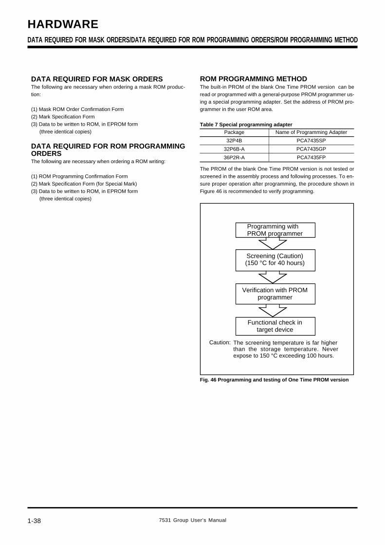
HARDWARE
7531 Group User’s Manual1-38
DATA REQUIRED FOR MASK ORDERSThe following are necessary when ordering a mask ROM produc-tion:
(1) Mask ROM Order Confirmation Form(2) Mark Specification Form(3) Data to be written to ROM, in EPROM form
(three identical copies)
DATA REQUIRED FOR ROM PROGRAMMINGORDERSThe following are necessary when ordering a ROM writing:
(1) ROM Programming Confirmation Form(2) Mark Specification Form (for Special Mark)(3) Data to be written to ROM, in EPROM form
(three identical copies)
ROM PROGRAMMING METHODThe built-in PROM of the blank One Time PROM version can beread or programmed with a general-purpose PROM programmer us-ing a special programming adapter. Set the address of PROM pro-grammer in the user ROM area.
The PROM of the blank One Time PROM version is not tested orscreened in the assembly process and following processes. To en-sure proper operation after programming, the procedure shown inFigure 46 is recommended to verify programming.
Package
32P4B
32P6B-A
36P2R-A
Name of Programming Adapter
PCA7435SP
PCA7435GP
PCA7435FP
Table 7 Special programming adapter
Fig. 46 Programming and testing of One Time PROM version
Programming with PROM programmer
Screening (Caution)(150 °C for 40 hours)
Verification with PROM programmer
Functional check in target device
The screening temperature is far higher than the storage temperature. Never expose to 150 °C exceeding 100 hours.
Caution:
DATA REQUIRED FOR MASK ORDERS/DATA REQUIRED FOR ROM PROGRAMMING ORDERS/ROM PROGRAMMING METHOD
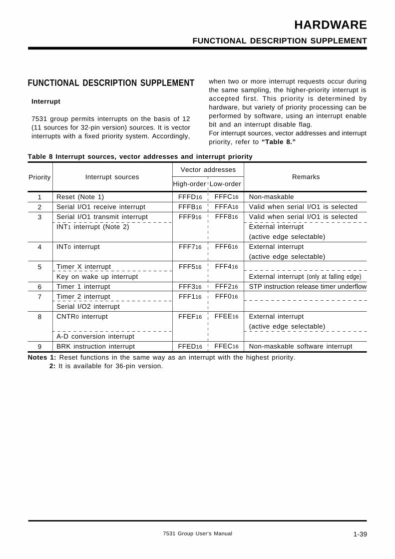
7531 Group User’s Manual 1-39
HARDWARE
Interrupt
7531 group permits interrupts on the basis of 12(11 sources for 32-pin version) sources. It is vectorinterrupts with a fixed priority system. Accordingly,
when two or more interrupt requests occur duringthe same sampling, the higher-priority interrupt isaccepted first. This priority is determined byhardware, but variety of priority processing can beperformed by software, using an interrupt enablebit and an interrupt disable flag.For interrupt sources, vector addresses and interruptpriority, refer to “Table 8.”
Vector addresses
FFFD16
FFFB16
FFF916
FFF716
FFF516
FFF316
FFF116
FFEF16
FFED16
FFFC16
FFFA16
FFF816
FFF616
FFF416
FFF216
FFF016
FFEE16
FFEC16
Table 8 Interrupt sources, vector addresses and interrupt priority
High-order Low-order
FUNCTIONAL DESCRIPTION SUPPLEMENT
Priority
1
2
3
4
5
6
7
8
9
Interrupt sources
Reset (Note 1)
Serial I/O1 receive interrupt
Serial I/O1 transmit interrupt
INT1 interrupt (Note 2)
INT0 interrupt
Timer X interrupt
Key on wake up interrupt
Timer 1 interrupt
Timer 2 interrupt
Serial I/O2 interrupt
CNTR0 interrupt
A-D conversion interrupt
BRK instruction interrupt
Remarks
Non-maskable
Valid when serial I/O1 is selected
Valid when serial I/O1 is selected
External interrupt
(active edge selectable)
External interrupt
(active edge selectable)
External interrupt (only at falling edge)
STP instruction release timer underflow
External interrupt
(active edge selectable)
Non-maskable software interrupt
Notes 1: Reset functions in the same way as an interrupt with the highest priority.2: It is available for 36-pin version.
FUNCTIONAL DESCRIPTION SUPPLEMENT
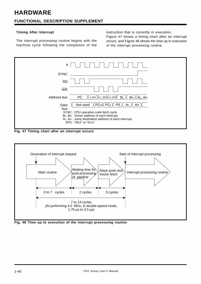
HARDWARE
7531 Group User’s Manual1-40
Timing After Interrupt
The interrupt processing routine begins with themachine cycle following the completion of the
instruction that is currently in execution.Figure 47 shows a timing chart after an interruptoccurs, and Figure 48 shows the time up to executionof the interrupt processing routine.
Fig. 47 Timing chart after an interrupt occurs
Fig. 48 Time up to execution of the interrupt processing routine
FUNCTIONAL DESCRIPTION SUPPLEMENT
: CPU operation code fetch cycle: Vector address of each interrupt: Jump destination address of each interrupt: “0016” or “0116”
SYNCBL, BHAL, AH
SPS
Data bus
Not used PCH PCL PS AL AH
Address bus S, SPS S-2, SPSS-1, SPSPC BL BH AL, AH
SYNC
RD
WR
φ
Generation of interrupt request
Main routine Interrupt processing routine
7 to 14 cycles(At performing 4.0 MHz, in double-speed mode,
1.75 µs to 3.5 µs)
2 cycles 5 cycles
Start of interrupt processing
0 to 7 cycles
Waiting time for post-processing of pipeline
Stack push and Vector fetch
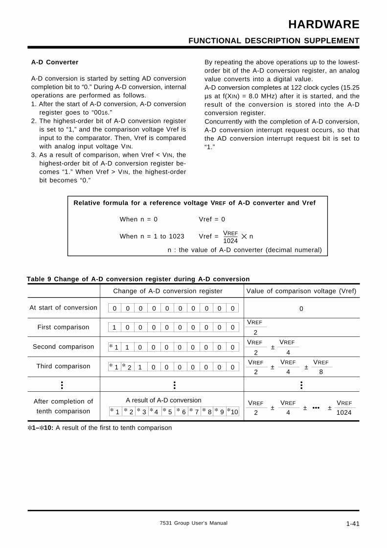
7531 Group User’s Manual 1-41
HARDWARE
A-D Converter
A-D conversion is started by setting AD conversioncompletion bit to “0.” During A-D conversion, internaloperations are performed as follows.1. After the start of A-D conversion, A-D conversion
register goes to “0016.”2. The highest-order bit of A-D conversion register
is set to “1,” and the comparison voltage Vref isinput to the comparator. Then, Vref is comparedwith analog input voltage VIN.
3. As a result of comparison, when Vref < VIN, thehighest-order bit of A-D conversion register be-comes “1.” When Vref > VIN, the highest-orderbit becomes “0.”
By repeating the above operations up to the lowest-order bit of the A-D conversion register, an analogvalue converts into a digital value.A-D conversion completes at 122 clock cycles (15.25µs at f(XIN) = 8.0 MHz) after it is started, and theresult of the conversion is stored into the A-Dconversion register.Concurrently with the completion of A-D conversion,A-D conversion interrupt request occurs, so thatthe AD conversion interrupt request bit is set to“1.”
Relative formula for a reference voltage V REF of A-D converter and Vref
When n = 0 Vref = 0
When n = 1 to 1023 Vref = n
n : the value of A-D converter (decimal numeral)
VREF
1024
1–10: A result of the first to tenth comparison
Table 9 Change of A-D conversion register during A-D conversion
At start of conversion
First comparison
Second comparison
Third comparison
After completion of
tenth comparison
1 0 0 0 0 0
1 0 0 0 0 0 0
1 0 0 0 0 0 0 0
0 0 0 0 0 00 0
VREF
2
VREF
4
VREF±
2
2 84
VREF VREF VREF± ±
A result of A-D conversion
1
1 2
1 2 3 4 5 6 7 8
Change of A-D conversion register Value of comparison voltage (Vref)
FUNCTIONAL DESCRIPTION SUPPLEMENT
0 00
0 0
0 0
0 0
9 10 2 10244
VREF VREF VREF± ±± •••
••••••
•••
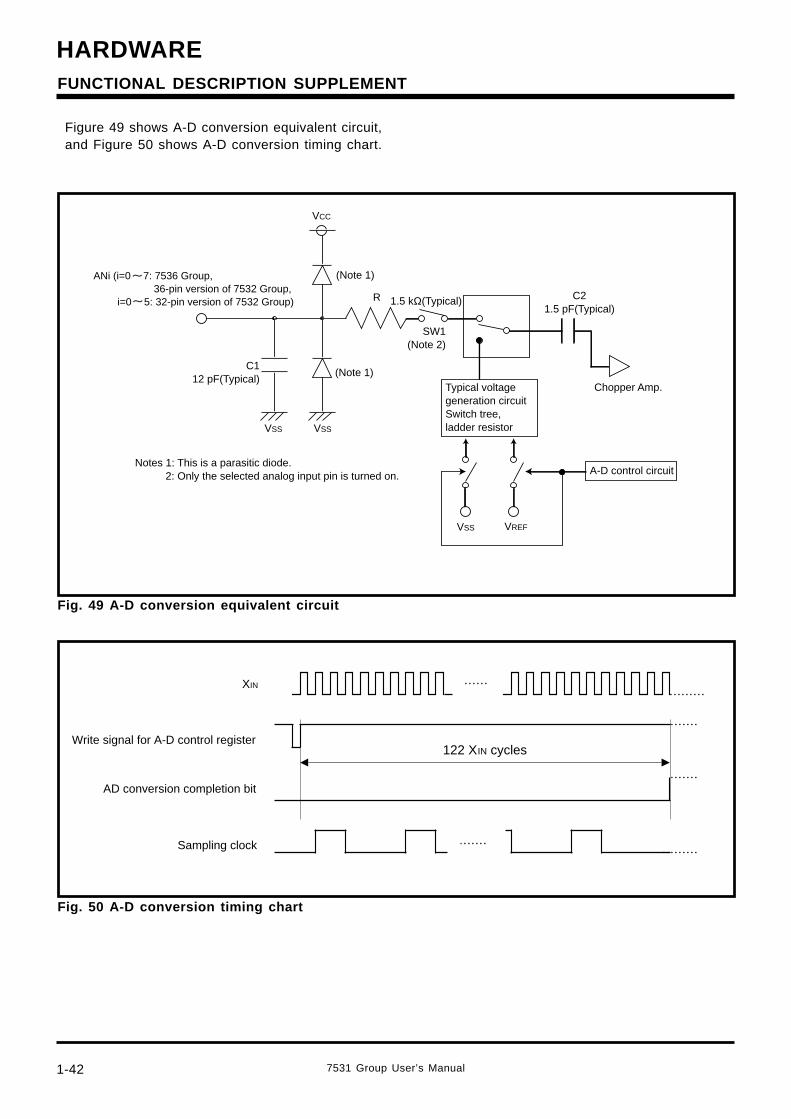
HARDWARE
7531 Group User’s Manual1-42
Figure 49 shows A-D conversion equivalent circuit,and Figure 50 shows A-D conversion timing chart.
Fig. 49 A-D conversion equivalent circuit
Fig. 50 A-D conversion timing chart
FUNCTIONAL DESCRIPTION SUPPLEMENT
ANi (i=0 7: 7536 Group, 36-pin version of 7532 Group,
i=0 5: 32-pin version of 7532 Group)
C112 pF(Typical)
Notes 1: This is a parasitic diode.2: Only the selected analog input pin is turned on.
C21.5 pF(Typical)
Chopper Amp.
A-D control circuit
Typical voltage generation circuitSwitch tree, ladder resistor
1.5 kΩ(Typical)
VSS VSS
VCC
VSS VREF
R
(Note 1)
SW1(Note 2)
(Note 1)
Write signal for A-D control register
AD conversion completion bit
Sampling clock
122 XIN cycles
XIN

CHAPTER 2CHAPTER 2APPLICATION
2.1 I/O port2.2 Timer2.3 Serial I/O2.4 A-D converter2.5 Reset
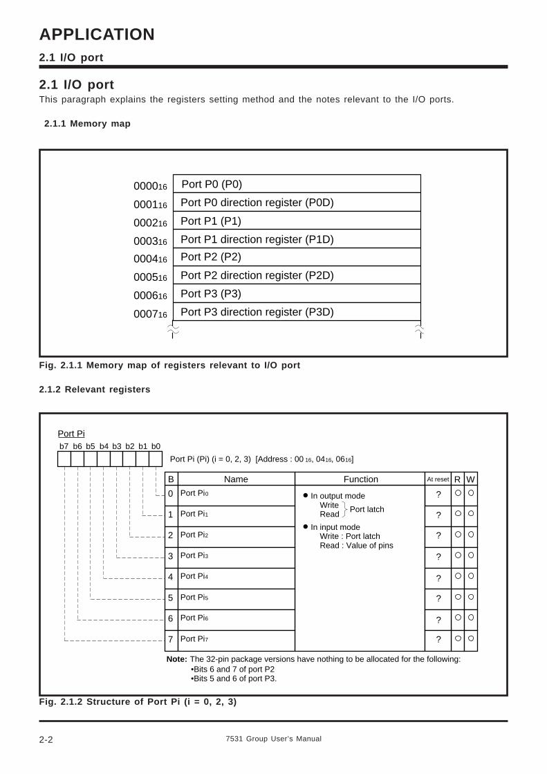
7531 Group User’s Manual2-2
APPLICATION2.1 I/O port
2.1 I/O portThis paragraph explains the registers setting method and the notes relevant to the I/O ports.
2.1.1 Memory map
Fig. 2.1.1 Memory map of registers relevant to I/O port
2.1.2 Relevant registers
000016
000116
000216
000316
000416
000516
000616
000716
Port P0 (P0)
Port P0 direction register (P0D)
Port P1 (P1)
Port P1 direction register (P1D)
Port P2 (P2)
Port P2 direction register (P2D)
Port P3 (P3)
Port P3 direction register (P3D)
Port Pib7 b6 b5 b4 b3 b2 b1 b0
B Function At reset R W
0
1
2
3
4
5
6
7
Name
Port Pi0
Port Pi1
Port Pi2
Port Pi3
Port Pi4
Port Pi5
Port Pi6
Port Pi7
In output mode Write Read
Port latch
In input mode Write : Port latch Read : Value of pins
Port Pi (Pi) (i = 0, 2, 3) [Address : 00 16, 0416, 0616]
?
?
?
?
?
?
?
?
Note: The 32-pin package versions have nothing to be allocated for the following:•Bits 6 and 7 of port P2•Bits 5 and 6 of port P3.
Fig. 2.1.2 Structure of Port Pi (i = 0, 2, 3)
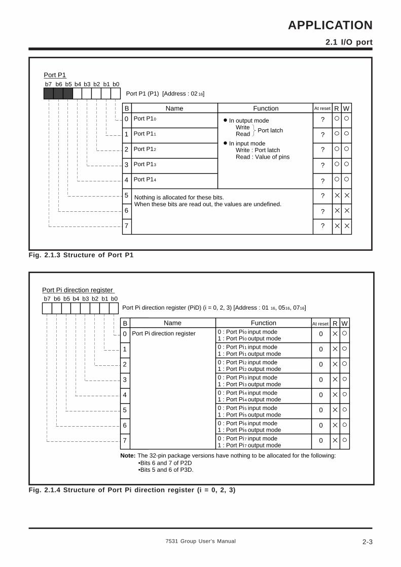
7531 Group User’s Manual
APPLICATION
2-3
2.1 I/O port
Port P1b7 b6 b5 b4 b3 b2 b1 b0
B Function At reset R W
0
1
2
3
4
5
6
7
Name
Port P10
Port P11
Port P12
Port P13
Port P14
In output mode Write Read
Port latch
In input mode Write : Port latch Read : Value of pins
Port P1 (P1) [Address : 02 16]
?
?
?
?
?
?
?
?
Nothing is allocated for these bits.When these bits are read out, the values are undefined.
Port Pi direction registerb7 b6 b5 b4 b3 b2 b1 b0
B Function At reset R W
0
1
2
3
4
5
6
7
Name
Port Pi direction register 0
0
0
0
0
0
0
0
Port Pi direction register (PiD) (i = 0, 2, 3) [Address : 01 16, 0516, 0716]
0 : Port Pi0 input mode1 : Port Pi0 output mode0 : Port Pi1 input mode1 : Port Pi1 output mode0 : Port Pi2 input mode1 : Port Pi2 output mode0 : Port Pi3 input mode1 : Port Pi3 output mode0 : Port Pi4 input mode1 : Port Pi4 output mode0 : Port Pi5 input mode1 : Port Pi5 output mode0 : Port Pi6 input mode1 : Port Pi6 output mode0 : Port Pi7 input mode1 : Port Pi7 output mode
Note: The 32-pin package versions have nothing to be allocated for the following:•Bits 6 and 7 of P2D•Bits 5 and 6 of P3D.
Fig. 2.1.3 Structure of Port P1
Fig. 2.1.4 Structure of Port Pi direction register (i = 0, 2, 3)
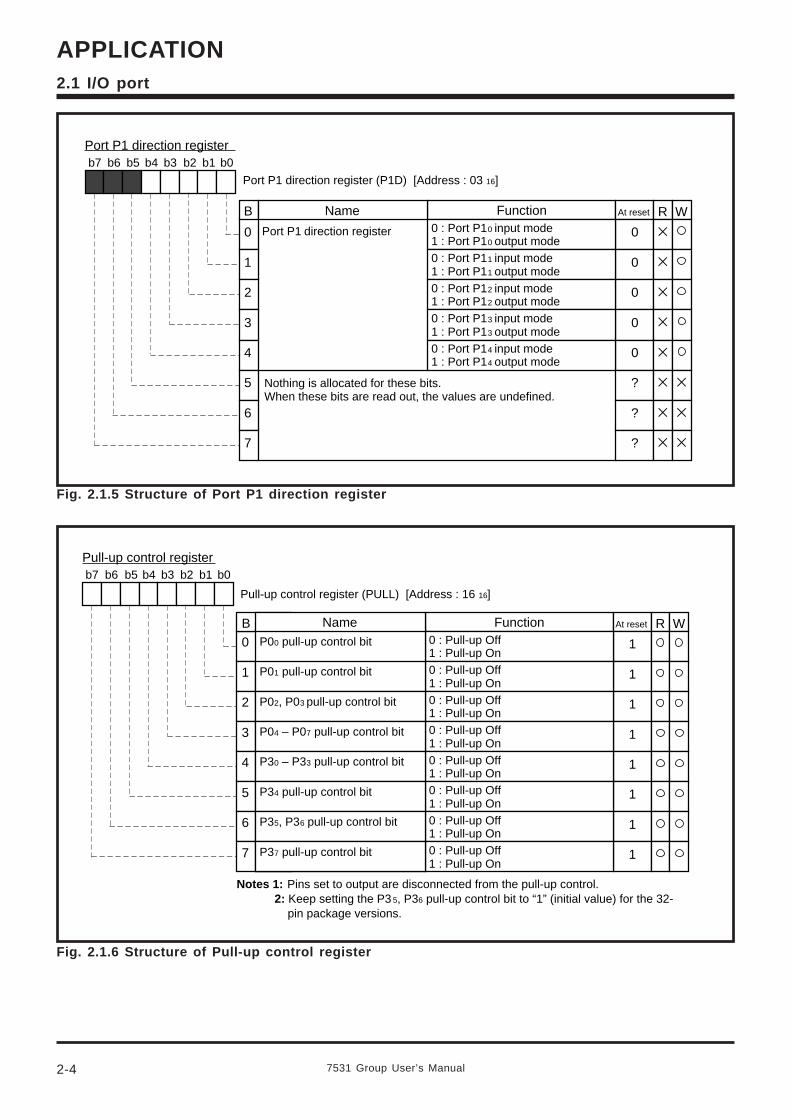
7531 Group User’s Manual2-4
APPLICATION2.1 I/O port
Fig. 2.1.5 Structure of Port P1 direction register
Port P1 direction registerb7 b6 b5 b4 b3 b2 b1 b0
B Function At reset R W
0
1
2
3
4
5
6
7
Name
Port P1 direction register 0
0
0
0
0
?
?
?
Port P1 direction register (P1D) [Address : 03 16]
0 : Port P10 input mode1 : Port P10 output mode0 : Port P11 input mode1 : Port P11 output mode0 : Port P12 input mode1 : Port P12 output mode0 : Port P13 input mode1 : Port P13 output mode0 : Port P14 input mode1 : Port P14 output mode
Nothing is allocated for these bits.When these bits are read out, the values are undefined.
Pull-up control registerb7 b6 b5 b4 b3 b2 b1 b0
B Function At reset R W0
1
2
3
4
5
6
7
NameP00 pull-up control bit 1
1
1
1
1
1
1
1
Pull-up control register (PULL) [Address : 16 16]
0 : Pull-up Off1 : Pull-up On
Notes 1: Pins set to output are disconnected from the pull-up control.2: Keep setting the P3 5, P36 pull-up control bit to “1” (initial value) for the 32-
pin package versions.
P01 pull-up control bit 0 : Pull-up Off1 : Pull-up On
P02, P03 pull-up control bit 0 : Pull-up Off1 : Pull-up On
P04 – P07 pull-up control bit 0 : Pull-up Off1 : Pull-up On
P30 – P33 pull-up control bit 0 : Pull-up Off1 : Pull-up On
P34 pull-up control bit 0 : Pull-up Off1 : Pull-up On
P35, P36 pull-up control bit 0 : Pull-up Off1 : Pull-up On
P37 pull-up control bit 0 : Pull-up Off1 : Pull-up On
Fig. 2.1.6 Structure of Pull-up control register
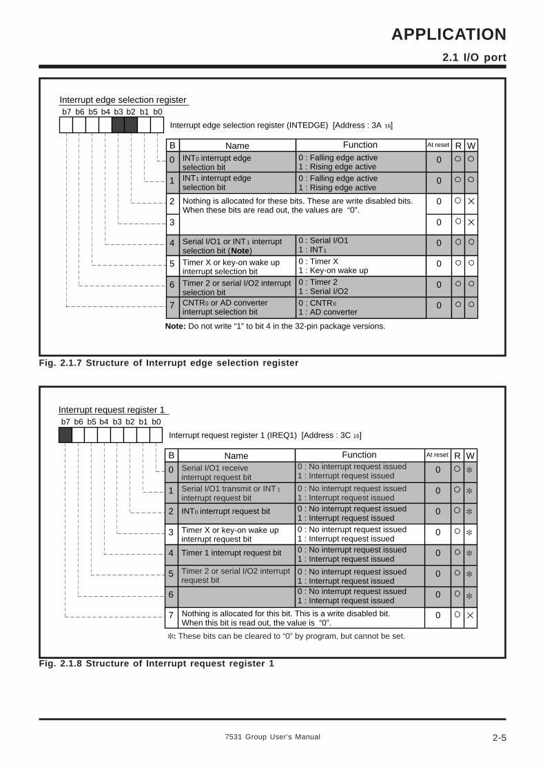
7531 Group User’s Manual
APPLICATION
2-5
2.1 I/O port
CNTR0 or AD converter interrupt request bit
Interrupt request register 1b7 b6 b5 b4 b3 b2 b1 b0
B Function At reset R W
0
1
2
3
4
5
6
7
Name
0
0
0
0
0
0
0
0
Interrupt request register 1 (IREQ1) [Address : 3C 16]
Nothing is allocated for this bit. This is a write disabled bit.When this bit is read out, the value is “0”.
Serial I/O1 receive interrupt request bitSerial I/O1 transmit or INT 1 interrupt request bit
0 : No interrupt request issued1 : Interrupt request issued
Timer 2 or serial I/O2 interrupt request bit
: These bits can be cleared to “0” by program, but cannot be set.
0 : No interrupt request issued1 : Interrupt request issued
INT0 interrupt request bit
Timer X or key-on wake up interrupt request bit
0 : No interrupt request issued1 : Interrupt request issued0 : No interrupt request issued1 : Interrupt request issued
Timer 1 interrupt request bit 0 : No interrupt request issued1 : Interrupt request issued
0 : No interrupt request issued1 : Interrupt request issued0 : No interrupt request issued1 : Interrupt request issued
Fig. 2.1.7 Structure of Interrupt edge selection register
Fig. 2.1.8 Structure of Interrupt request register 1
Interrupt edge selection registerb7 b6 b5 b4 b3 b2 b1 b0
B Function At reset R W
0
1
2
3
4
5
6
7
Name
0
0
0
0
0
0
0
0
Interrupt edge selection register (INTEDGE) [Address : 3A 16]
Nothing is allocated for these bits. These are write disabled bits.When these bits are read out, the values are “0”.
INT0 interrupt edge selection bitINT1 interrupt edge selection bit
0 : Falling edge active1 : Rising edge active0 : Falling edge active1 : Rising edge active
Serial I/O1 or INT1 interrupt selection bit (Note)Timer X or key-on wake up interrupt selection bitTimer 2 or serial I/O2 interrupt selection bitCNTR0 or AD converter interrupt selection bit
0 : Serial I/O11 : INT1
0 : Timer X1 : Key-on wake up0 : Timer 21 : Serial I/O20 : CNTR0
1 : AD converter
Note: Do not write “1” to bit 4 in the 32-pin package versions.
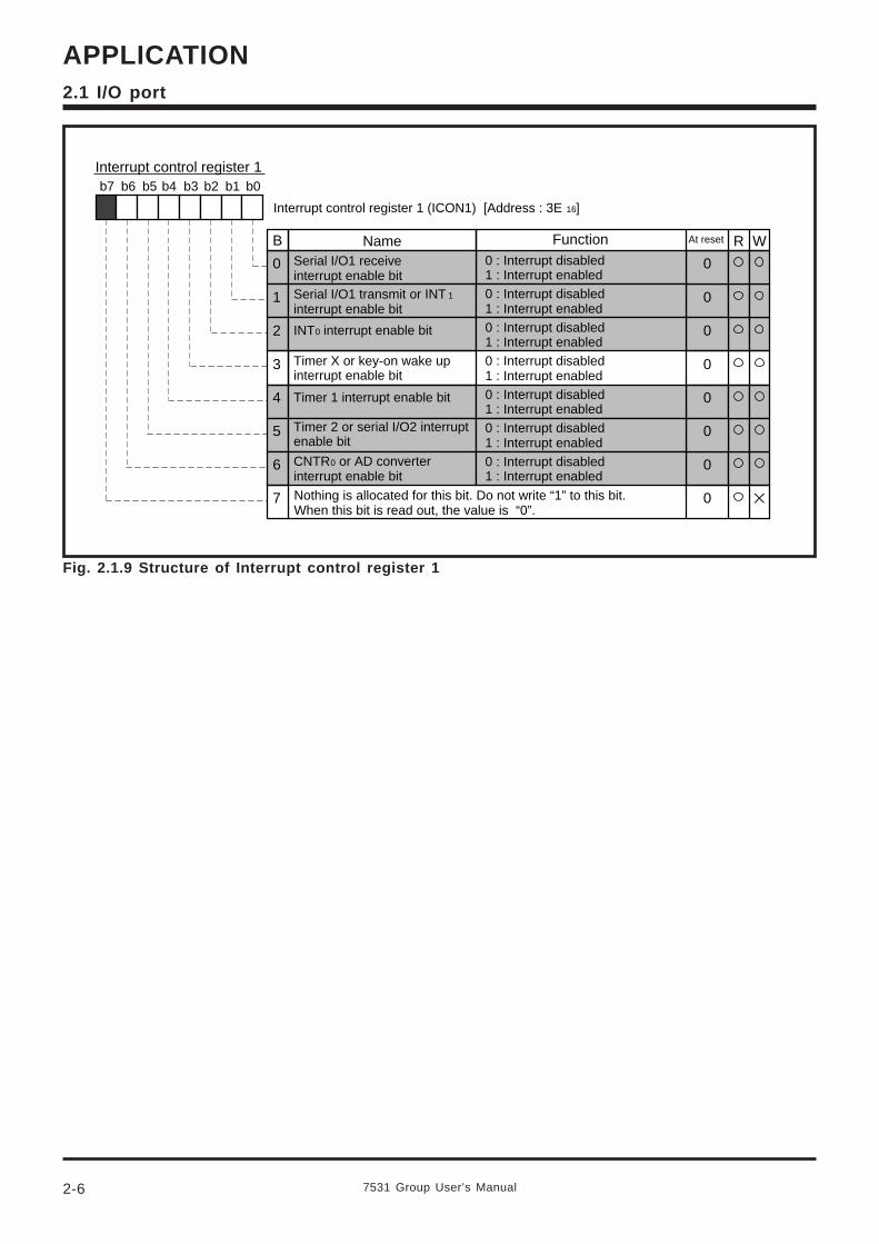
7531 Group User’s Manual2-6
APPLICATION2.1 I/O port
Interrupt control register 1b7 b6 b5 b4 b3 b2 b1 b0
B Function At reset R W
0
1
2
3
4
5
6
7
Name
0
0
0
0
0
0
0
0
Interrupt control register 1 (ICON1) [Address : 3E 16]
Nothing is allocated for this bit. Do not write “1” to this bit.When this bit is read out, the value is “0”.
Serial I/O1 receive interrupt enable bitSerial I/O1 transmit or INT 1 interrupt enable bit
0 : Interrupt disabled1 : Interrupt enabled
Timer 2 or serial I/O2 interrupt enable bit
CNTR0 or AD converter interrupt enable bit
INT0 interrupt enable bit
Timer X or key-on wake up interrupt enable bit
Timer 1 interrupt enable bit
0 : Interrupt disabled1 : Interrupt enabled0 : Interrupt disabled1 : Interrupt enabled0 : Interrupt disabled1 : Interrupt enabled0 : Interrupt disabled1 : Interrupt enabled0 : Interrupt disabled1 : Interrupt enabled0 : Interrupt disabled1 : Interrupt enabled
Fig. 2.1.9 Structure of Interrupt control register 1
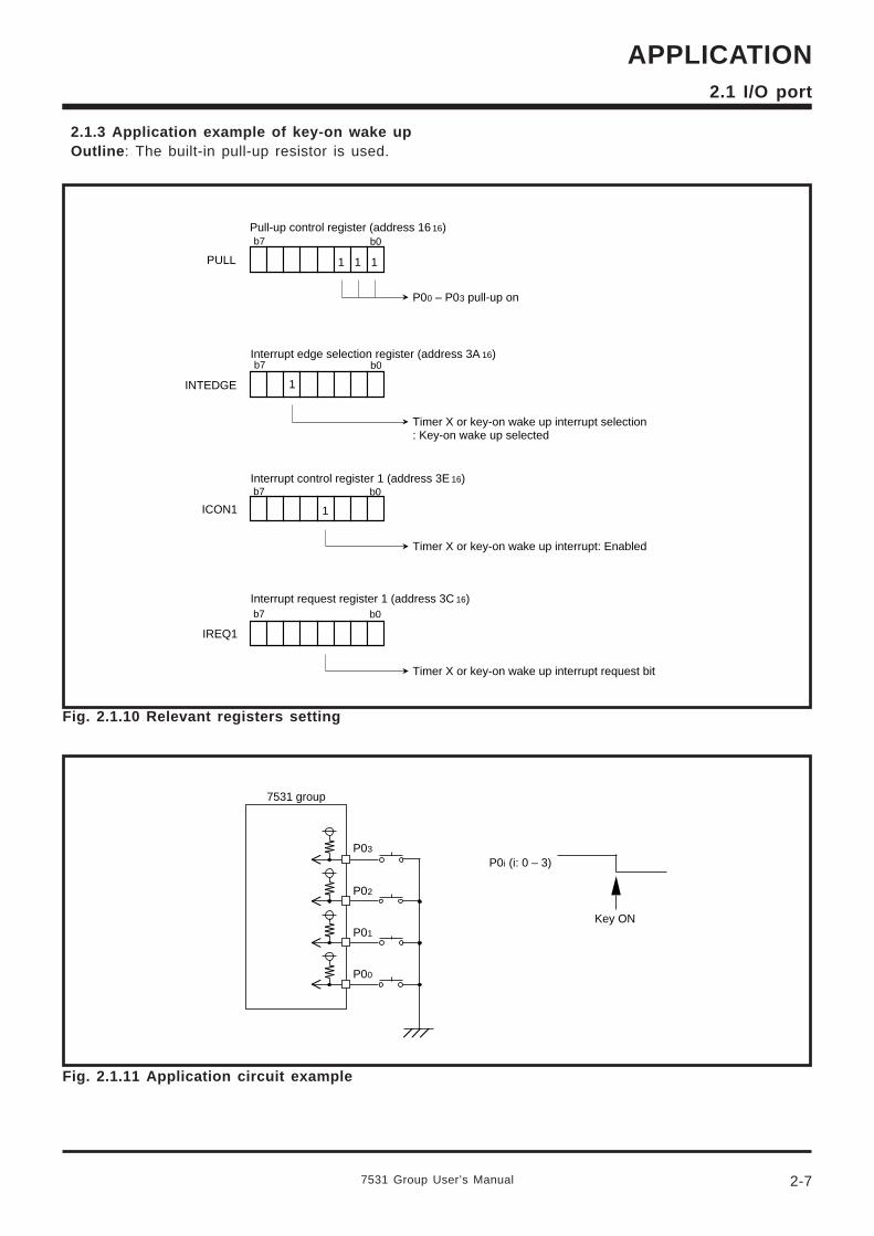
7531 Group User’s Manual
APPLICATION
2-7
2.1 I/O port
2.1.3 Application example of key-on wake upOutline: The built-in pull-up resistor is used.
Interrupt edge selection register (address 3A 16)
INTEDGE 1
IREQ1
Pull-up control register (address 16 16)
PULL 11
P00 – P03 pull-up on
1
b0b7
b0b7
b0b7
ICON1
b0b7
1
Timer X or key-on wake up interrupt selection: Key-on wake up selected
Interrupt control register 1 (address 3E 16)
Timer X or key-on wake up interrupt: Enabled
Interrupt request register 1 (address 3C 16)
Timer X or key-on wake up interrupt request bit
Fig. 2.1.10 Relevant registers setting
7531 group
P0i (i: 0 – 3)
Key ON
P03
P02
P01
P00
Fig. 2.1.11 Application circuit example
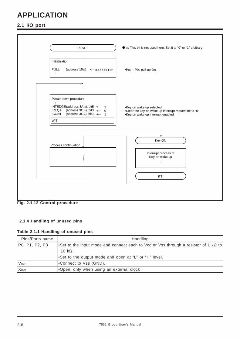
7531 Group User’s Manual2-8
APPLICATION2.1 I/O port
RESET
XXXXX1112
...
PULL (address 1616) •P03 – P00 pull-up On
101
WIT
Key ON
...
RTI
.......
...
Initialization
Power down procedure
...
INTEDGE(address 3A16), bit5IREQ1 (address 3C16), bit3ICON1 (address 3E16), bit3
Process continuation
Interrupt process ofKey-on wake up
: This bit is not used here. Set it to “0” or “1” arbitrary.
•Key-on wake up selected•Clear the key-on wake up interrupt request bit to “0”•Key-on wake up interrupt enabled
Fig. 2.1.12 Control procedure
2.1.4 Handling of unused pins
Table 2.1.1 Handling of unused pins
Pins/Ports name
P0, P1, P2, P3
VREF
XOUT
Handling
•Set to the input mode and connect each to Vcc or Vss through a resistor of 1 kΩ to
10 kΩ.
•Set to the output mode and open at “L” or “H” level.
•Connect to Vss (GND).
•Open, only when using an external clock
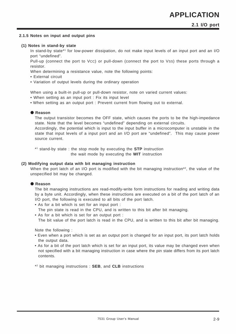
7531 Group User’s Manual
APPLICATION
2-9
2.1 I/O port
2.1.5 Notes on input and output pins
(1) Notes in stand-by stateIn stand-by state*1 for low-power dissipation, do not make input levels of an input port and an I/Oport “undefined”.Pull-up (connect the port to VCC) or pull-down (connect the port to VSS) these ports through aresistor.When determining a resistance value, note the following points:• External circuit• Variation of output levels during the ordinary operation
When using a built-in pull-up or pull-down resistor, note on varied current values:• When setting as an input port : Fix its input level• When setting as an output port : Prevent current from flowing out to external.
ReasonThe output transistor becomes the OFF state, which causes the ports to be the high-impedancestate. Note that the level becomes “undefined” depending on external circuits.Accordingly, the potential which is input to the input buffer in a microcomputer is unstable in thestate that input levels of a input port and an I/O port are “undefined”. This may cause powersource current.
*1 stand-by state : the stop mode by executing the STP instructionthe wait mode by executing the WIT instruction
(2) Modifying output data with bit managing instructionWhen the port latch of an I/O port is modified with the bit managing instruction*2, the value of theunspecified bit may be changed.
ReasonThe bit managing instructions are read-modify-write form instructions for reading and writing databy a byte unit. Accordingly, when these instructions are executed on a bit of the port latch of anI/O port, the following is executed to all bits of the port latch.• As for a bit which is set for an input port :
The pin state is read in the CPU, and is written to this bit after bit managing.• As for a bit which is set for an output port :
The bit value of the port latch is read in the CPU, and is written to this bit after bit managing.
Note the following :• Even when a port which is set as an output port is changed for an input port, its port latch holds
the output data.• As for a bit of the port latch which is set for an input port, its value may be changed even when
not specified with a bit managing instruction in case where the pin state differs from its port latchcontents.
*2 bit managing instructions : SEB, and CLB instructions
7531 Group User’s Manual2-10
APPLICATION2.1 I/O port
2.1.6 Termination of unused pins
(1) Terminate unused pins
➀ Output ports : Open
➁ Input ports :Connect each pin to VCC or VSS through each resistor of 1 kΩ to 10 kΩ.Ports that permit the selecting of a built-in pull-up or pull-down resistor can also use this resistor.As for pins whose potential affects to operation modes such as pins CNVSS, INT or others, selectthe VCC pin or the VSS pin according to their operation mode.
➂ I/O ports :• Set the I/O ports for the input mode and connect them to VCC or VSS through each resistor of
1 kΩ to 10 kΩ.Ports that permit the selecting of a built-in pull-up or pull-down resistor can also use this resistor.Set the I/O ports for the output mode and open them at “L” or “H”.
• When opening them in the output mode, the input mode of the initial status remains until themode of the ports is switched over to the output mode by the program after reset. Thus, thepotential at these pins is undefined and the power source current may increase in the inputmode. With regard to an effects on the system, thoroughly perform system evaluation on the userside.
• Since the direction register setup may be changed because of a program runaway or noise, setdirection registers by program periodically to increase the reliability of program.
(2) Termination remarks
➀ Input ports and I/O ports :Do not open in the input mode.
Reason• The power source current may increase depending on the first-stage circuit.• An effect due to noise may be easily produced as compared with proper termination ➁ and
➂ shown on the above.
➁ I/O ports :When setting for the input mode, do not connect to VCC or VSS directly.
ReasonIf the direction register setup changes for the output mode because of a program runaway ornoise, a short circuit may occur between a port and VCC (or VSS).
➂ I/O ports :When setting for the input mode, do not connect multiple ports in a lump to VCC or VSS througha resistor.
ReasonIf the direction register setup changes for the output mode because of a program runaway ornoise, a short circuit may occur between ports.
• At the termination of unused pins, perform wiring at the shortest possible distance (20 mm or less)from microcomputer pins.
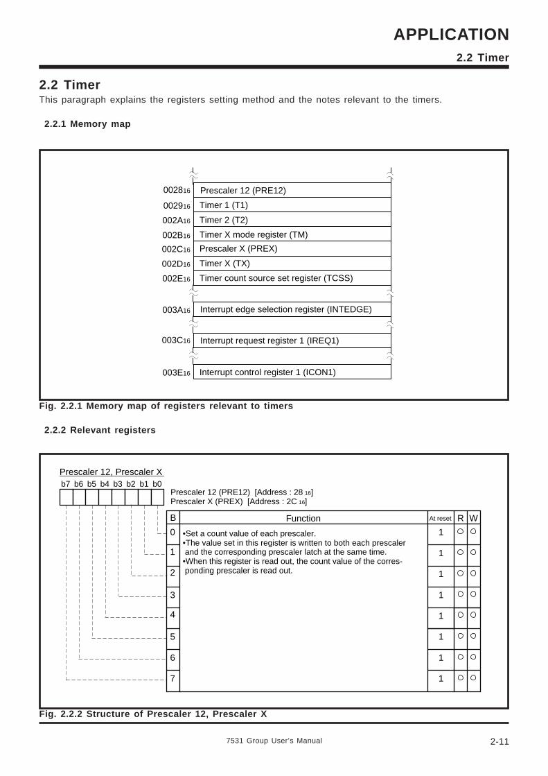
7531 Group User’s Manual
APPLICATION
2-11
2.2 Timer
2.2 TimerThis paragraph explains the registers setting method and the notes relevant to the timers.
2.2.1 Memory map
Fig. 2.2.1 Memory map of registers relevant to timers
2.2.2 Relevant registers
Fig. 2.2.2 Structure of Prescaler 12, Prescaler X
002816
002916
002A16
002B16
002C16
002D16
002E16
Prescaler 12 (PRE12)
Timer 1 (T1)
Timer 2 (T2)
Timer X mode register (TM)
Prescaler X (PREX)
Timer X (TX)
Timer count source set register (TCSS)
003C16
003E16
Interrupt request register 1 (IREQ1)
Interrupt control register 1 (ICON1)
003A16 Interrupt edge selection register (INTEDGE)
Prescaler 12, Prescaler Xb7 b6 b5 b4 b3 b2 b1 b0
B Function At reset R W
0
1
2
3
4
5
6
7
1
1
1
1
1
1
1
1
Prescaler 12 (PRE12) [Address : 28 16]Prescaler X (PREX) [Address : 2C 16]
•Set a count value of each prescaler.•The value set in this register is written to both each prescaler and the corresponding prescaler latch at the same time.•When this register is read out, the count value of the corres-ponding prescaler is read out.

7531 Group User’s Manual2-12
APPLICATION2.2 Timer
Fig. 2.2.3 Structure of Timer 1
Fig. 2.2.4 Structure of Timer 2
Timer 1b7 b6 b5 b4 b3 b2 b1 b0
B Function At reset R W
0
1
2
3
4
5
6
7
1
0
0
0
0
0
0
0
Timer 1 (T1) [Address : 29 16]
•Set a count value of timer 1.•The value set in this register is written to both timer 1 and timer 1
latch at the same time.•When this register is read out, the timer 1’s count value is read
out.
Timer 2b7 b6 b5 b4 b3 b2 b1 b0
B Function At reset R W
0
1
2
3
4
5
6
7
0
0
0
0
0
0
0
0
Timer 2 (T2) [Address : 2A 16]
•Set a count value of timer 2.•The value set in this register is written to both timer 2 and timer 2
latch at the same time.•When this register is read out, the timer 2’s count value is read
out.
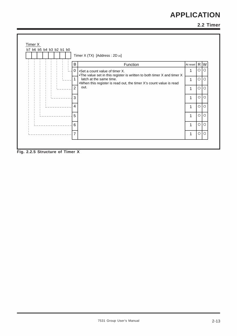
7531 Group User’s Manual
APPLICATION
2-13
2.2 Timer
Fig. 2.2.5 Structure of Timer X
Timer Xb7 b6 b5 b4 b3 b2 b1 b0
B Function At reset R W
0
1
2
3
4
5
6
7
1
1
1
1
1
1
1
1
Timer X (TX) [Address : 2D 16]
•Set a count value of timer X.•The value set in this register is written to both timer X and timer X
latch at the same time.•When this register is read out, the timer X’s count value is read
out.
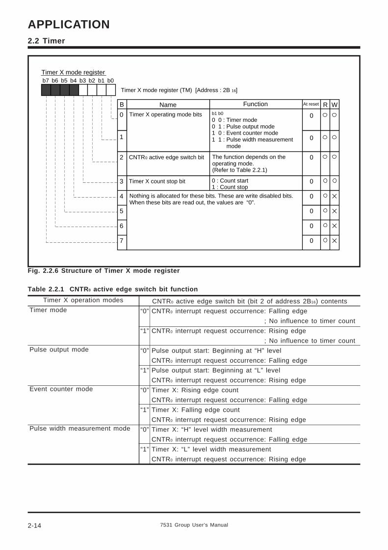
7531 Group User’s Manual2-14
APPLICATION2.2 Timer
Fig. 2.2.6 Structure of Timer X mode register
Timer X operation modes
Timer mode
Pulse output mode
Event counter mode
Pulse width measurement mode
CNTR0 active edge switch bit (bit 2 of address 2B16) contents
“0” CNTR0 interrupt request occurrence: Falling edge
; No influence to timer count
“1” CNTR0 interrupt request occurrence: Rising edge
; No influence to timer count
“0” Pulse output start: Beginning at “H” level
CNTR0 interrupt request occurrence: Falling edge
“1” Pulse output start: Beginning at “L” level
CNTR0 interrupt request occurrence: Rising edge
“0” Timer X: Rising edge count
CNTR0 interrupt request occurrence: Falling edge
“1” Timer X: Falling edge count
CNTR0 interrupt request occurrence: Rising edge
“0” Timer X: “H” level width measurement
CNTR0 interrupt request occurrence: Falling edge
“1” Timer X: “L” level width measurement
CNTR0 interrupt request occurrence: Rising edge
Table 2.2.1 CNTR0 active edge switch bit function
b7 b6 b5 b4 b3 b2 b1 b0
B Function At reset R W
0
2
3
4
5
6
7
Name
0
0
0
0
Timer X mode register (TM) [Address : 2B 16]
Nothing is allocated for these bits. These are write disabled bits.When these bits are read out, the values are “0”.
Timer X mode register
0
0
00 0 : Timer mode0 1 : Pulse output mode1 0 : Event counter mode1 1 : Pulse width measurement
mode
b1 b0
1 0
Timer X operating mode bits
CNTR0 active edge switch bit The function depends on the operating mode.(Refer to Table 2.2.1)
Timer X count stop bit 0 : Count start1 : Count stop
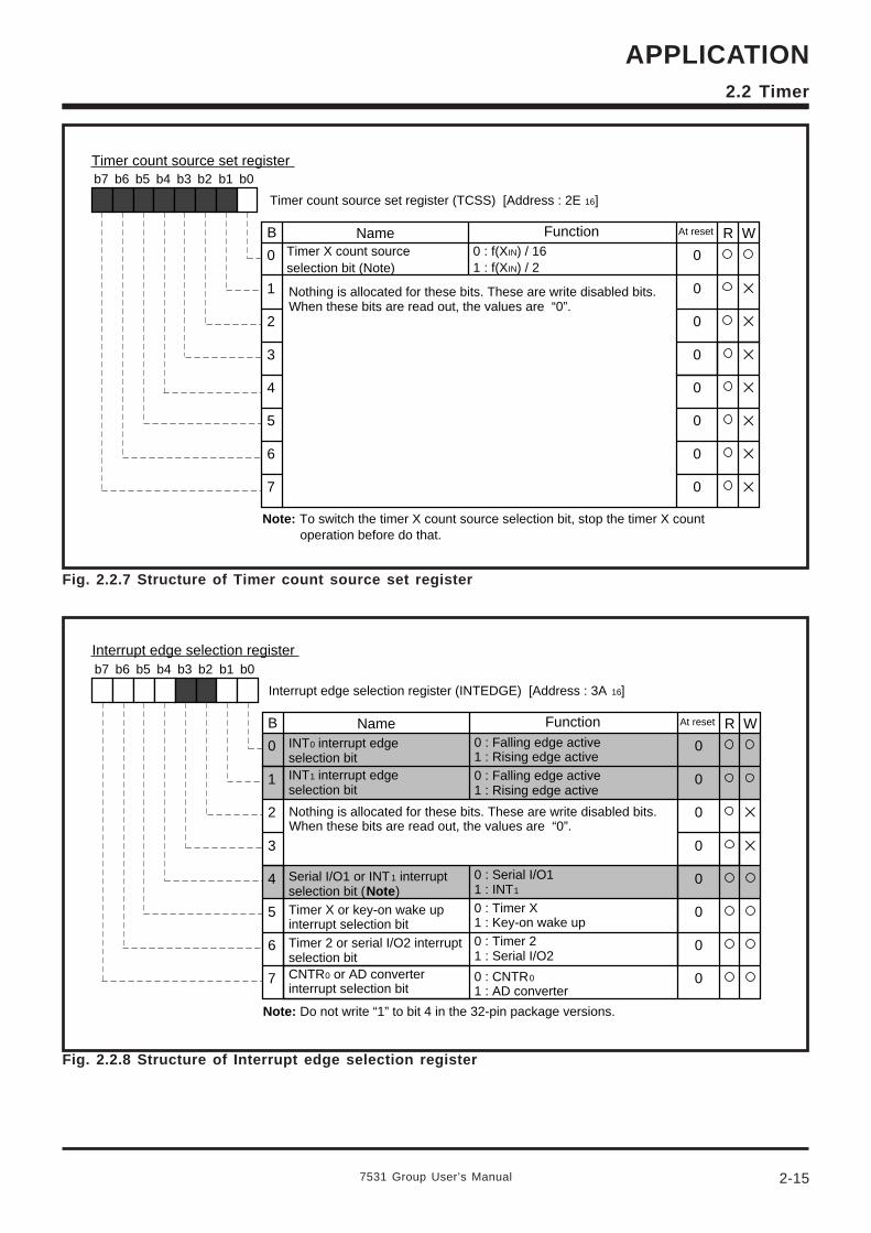
7531 Group User’s Manual
APPLICATION
2-15
2.2 Timer
Fig. 2.2.7 Structure of Timer count source set register
Fig. 2.2.8 Structure of Interrupt edge selection register
b7 b6 b5 b4 b3 b2 b1 b0
B Function At reset R W
0
1
2
3
4
5
6
7
Name
0
0
0
0
0
Timer count source set register (TCSS) [Address : 2E 16]
Nothing is allocated for these bits. These are write disabled bits.When these bits are read out, the values are “0”.
Timer count source set register
Timer X count source selection bit (Note)
0 : f(XIN) / 161 : f(XIN) / 2
0
0
0
Note: To switch the timer X count source selection bit, stop the timer X count operation before do that.
Interrupt edge selection registerb7 b6 b5 b4 b3 b2 b1 b0
B Function At reset R W
0
1
2
3
4
5
6
7
Name
0
0
0
0
0
0
0
0
Interrupt edge selection register (INTEDGE) [Address : 3A 16]
Nothing is allocated for these bits. These are write disabled bits.When these bits are read out, the values are “0”.
INT0 interrupt edge selection bitINT1 interrupt edge selection bit
0 : Falling edge active1 : Rising edge active0 : Falling edge active1 : Rising edge active
Serial I/O1 or INT1 interrupt selection bit (Note)Timer X or key-on wake up interrupt selection bitTimer 2 or serial I/O2 interrupt selection bitCNTR0 or AD converter interrupt selection bit
0 : Serial I/O11 : INT1
0 : Timer X1 : Key-on wake up0 : Timer 21 : Serial I/O2
0 : CNTR0
1 : AD converter
Note: Do not write “1” to bit 4 in the 32-pin package versions.
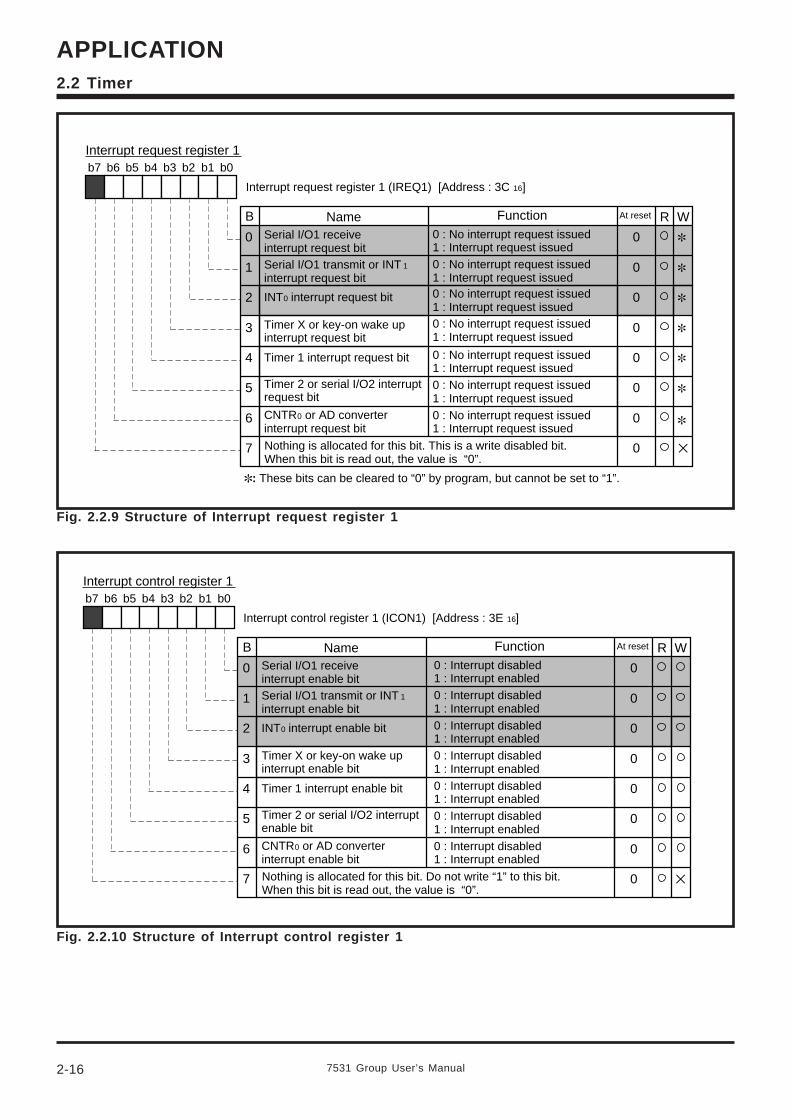
7531 Group User’s Manual2-16
APPLICATION2.2 Timer
Fig. 2.2.9 Structure of Interrupt request register 1
Interrupt request register 1b7 b6 b5 b4 b3 b2 b1 b0
B Function At reset R W
0
1
2
3
4
5
6
7
Name
0
0
0
0
0
0
0
0
Interrupt request register 1 (IREQ1) [Address : 3C 16]
Nothing is allocated for this bit. This is a write disabled bit.When this bit is read out, the value is “0”.
Serial I/O1 receive interrupt request bitSerial I/O1 transmit or INT 1 interrupt request bit
0 : No interrupt request issued1 : Interrupt request issued
Timer 2 or serial I/O2 interrupt request bit
CNTR0 or AD converter interrupt request bit
: These bits can be cleared to “0” by program, but cannot be set to “1”.
0 : No interrupt request issued1 : Interrupt request issued
INT0 interrupt request bit
Timer X or key-on wake up interrupt request bit
0 : No interrupt request issued1 : Interrupt request issued0 : No interrupt request issued1 : Interrupt request issued
Timer 1 interrupt request bit 0 : No interrupt request issued1 : Interrupt request issued0 : No interrupt request issued1 : Interrupt request issued0 : No interrupt request issued1 : Interrupt request issued
Interrupt control register 1b7 b6 b5 b4 b3 b2 b1 b0
B Function At reset R W
0
1
2
3
4
5
6
7
Name
0
0
0
0
0
0
0
0
Interrupt control register 1 (ICON1) [Address : 3E 16]
Nothing is allocated for this bit. Do not write “1” to this bit.When this bit is read out, the value is “0”.
Serial I/O1 receive interrupt enable bitSerial I/O1 transmit or INT 1 interrupt enable bit
0 : Interrupt disabled1 : Interrupt enabled
Timer 2 or serial I/O2 interrupt enable bit
CNTR0 or AD converter interrupt enable bit
INT0 interrupt enable bit
Timer X or key-on wake up interrupt enable bit
Timer 1 interrupt enable bit
0 : Interrupt disabled1 : Interrupt enabled0 : Interrupt disabled1 : Interrupt enabled0 : Interrupt disabled1 : Interrupt enabled0 : Interrupt disabled1 : Interrupt enabled0 : Interrupt disabled1 : Interrupt enabled0 : Interrupt disabled1 : Interrupt enabled
Fig. 2.2.10 Structure of Interrupt control register 1
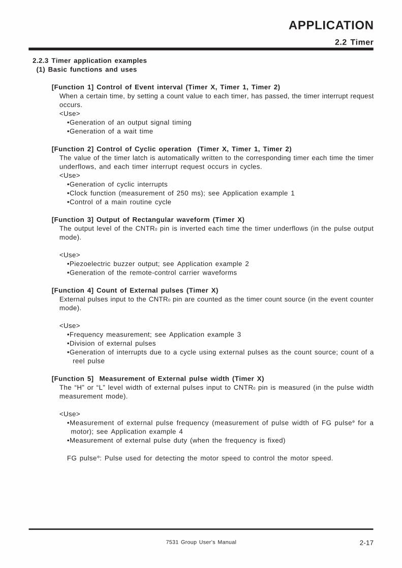
7531 Group User’s Manual
APPLICATION
2-17
2.2 Timer
2.2.3 Timer application examples(1) Basic functions and uses
[Function 1] Control of Event interval (Timer X, Timer 1, Timer 2)When a certain time, by setting a count value to each timer, has passed, the timer interrupt requestoccurs.<Use>
•Generation of an output signal timing•Generation of a wait time
[Function 2] Control of Cyclic operation (Timer X, Timer 1, Timer 2)The value of the timer latch is automatically written to the corresponding timer each time the timerunderflows, and each timer interrupt request occurs in cycles.<Use>
•Generation of cyclic interrupts•Clock function (measurement of 250 ms); see Application example 1•Control of a main routine cycle
[Function 3] Output of Rectangular waveform (Timer X)The output level of the CNTR0 pin is inverted each time the timer underflows (in the pulse outputmode).
<Use>•Piezoelectric buzzer output; see Application example 2•Generation of the remote-control carrier waveforms
[Function 4] Count of External pulses (Timer X)External pulses input to the CNTR0 pin are counted as the timer count source (in the event countermode).
<Use>•Frequency measurement; see Application example 3•Division of external pulses•Generation of interrupts due to a cycle using external pulses as the count source; count of a
reel pulse
[Function 5] Measurement of External pulse width (Timer X)The “H” or “L” level width of external pulses input to CNTR0 pin is measured (in the pulse widthmeasurement mode).
<Use>•Measurement of external pulse frequency (measurement of pulse width of FG pulse for a
motor); see Application example 4•Measurement of external pulse duty (when the frequency is fixed)
FG pulse: Pulse used for detecting the motor speed to control the motor speed.
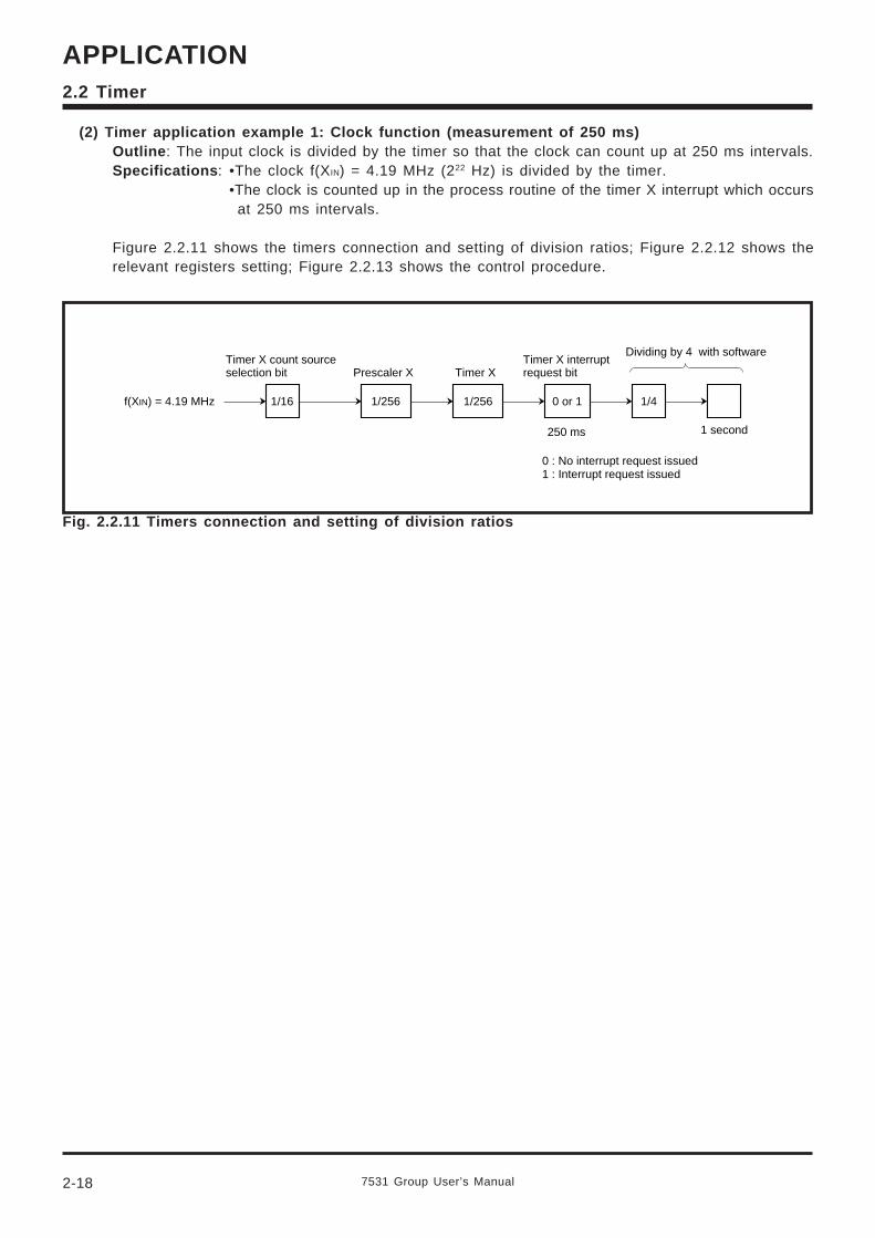
7531 Group User’s Manual2-18
APPLICATION2.2 Timer
(2) Timer application example 1: Clock function (measurement of 250 ms)Outline : The input clock is divided by the timer so that the clock can count up at 250 ms intervals.Specifications : •The clock f(XIN) = 4.19 MHz (222 Hz) is divided by the timer.
•The clock is counted up in the process routine of the timer X interrupt which occursat 250 ms intervals.
Figure 2.2.11 shows the timers connection and setting of division ratios; Figure 2.2.12 shows therelevant registers setting; Figure 2.2.13 shows the control procedure.
Fig. 2.2.11 Timers connection and setting of division ratios
f(XIN) = 4.19 MHz
250 ms
1/16 1/256 1/256 1/4
1 second
Dividing by 4 with softwareTimer X count source selection bit Prescaler X Timer X
Timer X interrupt request bit
0 or 1
0 : No interrupt request issued1 : Interrupt request issued
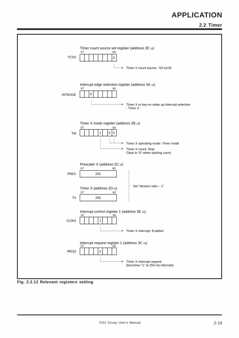
7531 Group User’s Manual
APPLICATION
2-19
2.2 Timer
Fig. 2.2.12 Relevant registers setting
ICON1
Timer X interrupt: Enabled
1
IREQ1
TM 001
PREX 255
TX 255
b0b7
b0b7
b0b7
b0b7
b0b7
INTEDGE 0
b0b7
TCSS 0
Timer X count source : f(X IN)/16
b0b7
0
Timer count source set register (address 2E 16)
Timer X or key-on wake up interrupt selection: Timer X
Interrupt edge selection register (address 3A 16)
Timer X mode register (address 2B 16)
Timer X operating mode: Timer mode
Timer X count: StopClear to “0” when starting count.
Prescaler X (address 2C 16)
Timer X (address 2D 16)Set “division ratio – 1”
Interrupt control register 1 (address 3E 16)
Interrupt request register 1 (address 3C 16)
Timer X interrupt request(becomes “1” at 250 ms intervals)
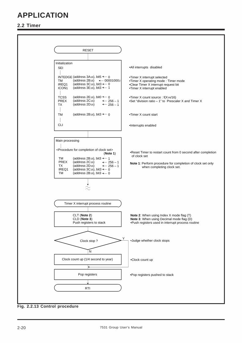
7531 Group User’s Manual2-20
APPLICATION2.2 Timer
Fig. 2.2.13 Control procedure
RESET
Initialization
SEI
INTEDGETMIREQ1ICON1
TCSSPREXTX
TM
CLI
0
01
..........
.....
0256 – 1256 – 1
Main processing
TMPREXTXIREQ1TM
.....
1256 – 1256 – 100
Clock stop ?
N
Y
RTI
(address 2B16), bit3(address 2C16)(address 2D16)(address 3C16), bit3(address 2B16), bit3
(address 3A16), bit5(address 2B16)(address 3C16), bit3(address 3E16), bit3
CLT (Note 2)CLD (Note 3)Push registers to stack
(address 2E16), bit0(address 2C16)(address 2D16)
(address 2B16), bit3 0
.....
<Procedure for completion of clock set> (Note 1)
Timer X interrupt process routine
Clock count up (1/4 second to year)
Pop registers
000010002
•All interrupts disabled
•Timer X interrupt selected•Timer X operating mode : Timer mode•Clear Timer X interrupt request bit•Timer X interrupt enabled
•Timer X count source : f(X IN/16)•Set “division ratio – 1” to Prescaler X and Timer X
•Timer X count start
•Interrupts enabled
•Reset Timer to restart count from 0 second after completion of clock set
Note 1: Perform procedure for completion of clock set only when completing clock set.
Note 2: When using Index X mode flag (T)Note 3: When using Decimal mode flag (D)•Push registers used in interrupt process routine
•Judge whether clock stops
•Clock count up
•Pop registers pushed to stack
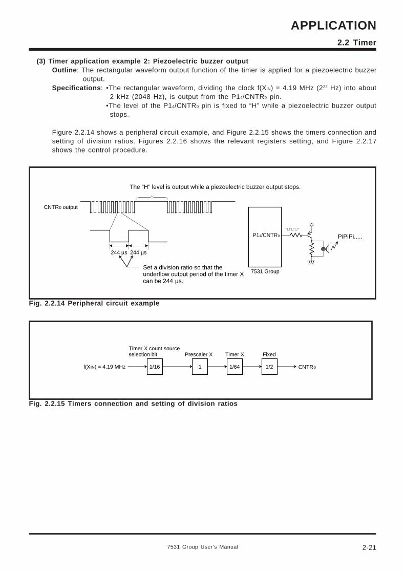
7531 Group User’s Manual
APPLICATION
2-21
2.2 Timer
(3) Timer application example 2: Piezoelectric buzzer outputOutline : The rectangular waveform output function of the timer is applied for a piezoelectric buzzer
output.Specifications : •The rectangular waveform, dividing the clock f(XIN) = 4.19 MHz (222 Hz) into about
2 kHz (2048 Hz), is output from the P14/CNTR0 pin.•The level of the P14/CNTR0 pin is fixed to “H” while a piezoelectric buzzer output
stops.
Figure 2.2.14 shows a peripheral circuit example, and Figure 2.2.15 shows the timers connection andsetting of division ratios. Figures 2.2.16 shows the relevant registers setting, and Figure 2.2.17shows the control procedure.
7531 Group
P14/CNTR0 PiPiPi.....
244 µs
CNTR0 output
The “H” level is output while a piezoelectric buzzer output stops.
244 µs
Set a division ratio so that the underflow output period of the timer X can be 244 µs.
Fig. 2.2.14 Peripheral circuit example
1/16 1/64 1/2 CNTR01f(XIN) = 4.19 MHz
Timer X count source selection bit Prescaler X Timer X Fixed
Fig. 2.2.15 Timers connection and setting of division ratios
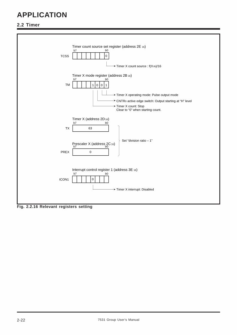
7531 Group User’s Manual2-22
APPLICATION2.2 Timer
Fig. 2.2.16 Relevant registers setting
TM
TX 63
1001
PREX 0
b0b7
b0b7
b0b7
TCSS 0
b0b7
ICON1 0
b0b7
Timer X interrupt: Disabled
Timer X count source : f(X IN)/16
Timer count source set register (address 2E 16)
Timer X mode register (address 2B 16)
Timer X operating mode: Pulse output mode
Timer X count: StopClear to “0” when starting count.
Prescaler X (address 2C 16)
Timer X (address 2D 16)
Set “division ratio – 1”
Interrupt control register 1 (address 3E 16)
CNTR0 active edge switch: Output starting at “H” level
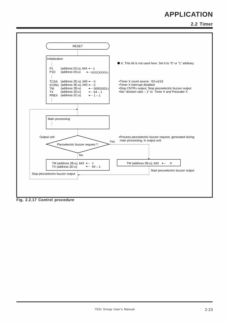
7531 Group User’s Manual
APPLICATION
2-23
2.2 Timer
Fig. 2.2.17 Control procedure
RESET
P1P1D
TCSSICON1TMTXPREX
1
..........
.....
00000010012
64 – 11 – 1
.....
Output unit
TM (address 2B16), bit3 0
(address 0216), bit4(address 0316)
(address 2E16), bit0(address 3E16), bit3(address 2B16)(address 2D16)(address 2C16)
TM (address 2B16), bit3 1TX (address 2D16) 64 – 1
Initialization
: This bit is not used here. Set it to “0” or “1” arbitrary.
XXX1XXXX2
Main processing
Piezoelectric buzzer request ?Yes
Start piezoelectric buzzer outputStop piezoelectric buzzer output
No
•Timer X count source : f(X IN)/16•Timer X interrupt disabled•Stop CNTR0 output; Stop piezoelectric buzzer output•Set “division ratio – 1” to Timer X and Prescaler X
•Process piezoelectric buzzer request, generated during main processing, in output unit
7531 Group User’s Manual2-24
APPLICATION2.2 Timer
(4) Timer application example 3: Frequency measurementOutline : The following two values are compared to judge whether the frequency is within a valid
range.•A value by counting pulses input to P14/CNTR0 pin with the timer.•A reference value
Specifications : •The pulse is input to the P14/CNTR0 pin and counted by the timer X.•A count value is read out at about 2 ms intervals, the timer 1 interrupt interval.When the count value is 28 to 40, it is judged that the input pulse is valid.•Because the timer is a down-counter, the count value is compared with 227 to 215(Note).
Note : 227 to 215 = 255 (initial value of counter) – 28 to 255 – 40; 28 to 40 means the numberof valid value.
Figure 2.2.18 shows the judgment method of valid/invalid of input pulses; Figure 2.2.19 shows therelevant registers setting; Figure 2.2.20 shows the control procedure.
Fig 2.2.18 Judgment method of valid/invalid of input pulses
Input pulse
2 ms71.4 µs
= 28 counts
@ @ @ @ @ @ @ @ @ @ @ @
71.4 µs or more(14 kHz or less)
71.4 µs(14 kHz)
50 µs(20 kHz)
50 µs or less (20 kHz or more)
Invalid Valid Invalid
2 ms50 µs
= 40 counts
7531 Group User’s Manual
APPLICATION
2-25
2.2 Timer
Fig. 2.2.19 Relevant registers setting
TM
PRE12 63
T1
1 01 1
PREX
TX
7
0
255
ICON1 0
IREQ1 0
b0b7
b0b7
b0b7
b0b7
b0b7
b0b7
b0b7
INTEDGE 0
b0b7
1
Timer X interrupt: Disabled
Timer X mode register (address 2B 16)
Timer X operating mode: Event counter mode
Timer X count: StopClear to “0” when starting count
Prescaler 12 (address 28 16)
Timer X (address 2D 16)
Set “division ratio – 1”
Interrupt control register 1 (address 3E 16)
CNTR0 active edge switch: Falling edge count
Timer X or key-on wake up interrupt selection: Timer X
Interrupt edge selection register (address 3A 16)
Prescaler X (address 2C 16)
Timer 1 (address 2916)
Timer 1 interrupt: Enabled
Interrupt request register 1 (address 3C 16)
Judgment of Timer X interrupt request bit( “1” of this bit when reading the count value indicates the 256 or more pulses input in the condition of Timer X = 255)
Set 255 just before counting pulses(After a certain time has passed, the number of input pulses is decreased from this value.)
7531 Group User’s Manual2-26
APPLICATION2.2 Timer
RESET
SEI
INTEDGETMPRE12T1PREXTXICON1
TM
CLI
0
..........
0
IREQ1(address 3C16), bit3 ?
0
1
RTI
.....
TX (address 2D16)(A)
214 < (A) < 228
0Fpulse 1Fpulse
TX (address 2D16)IREQ1 (address 3C16), bit3
256 – 10
(address 3A16), bit5(address 2B16)(address 2816)(address 2916)(address 2C16)(address 2D16)(address 3E16)
(address 2B16), bit3
: This bit is not used here. Set it to “0” or “1” arbitrary.
•All interrupts disabled
•Timer X interrupt selected•Timer X operating mode : Event counter mode(Count a falling edge of pulses input from CNTR 0 pin.)
•Set division ratio so that Timer 1 interrupt will occur at2 ms intervals.
•Timer X count start
•Interrupts enabled
Note 1: When using Index X mode flag (T)Note 2: When using Decimal mode flag (D)•Push registers used in interrupt process routine
•Pop registers pushed to stack
•Initialize the counter value•Clear Timer X interrupt request bit
Initialization
000011102
64 – 18 – 11 – 1256 – 10XX10XXX2 •Timer 1 interrupt enabled
•Timer X interrupt disabled
Timer 1 interrupt process routine
CLT (Note 1)CLD (Note 2)Push registers to stack
•Process as out of range when the count value is 256 or more
•Read the count value•Store the count value into Accumulator (A)
In range
Out of range
•Compare the read value with reference value
•Store the comparison result toflag Fpulse
Process judgment result
Pop registers
Fig. 2.2.20 Control procedure
7531 Group User’s Manual
APPLICATION
2-27
2.2 Timer
(5) Timer application example 4: Measurement of FG pulse width for motorOutline : The timer X counts the “H” level width of the pulses input to the P14/CNTR0 pin. An
underflow is detected by the timer X interrupt and an end of the input pulse “H” level isdetected by the CNTR0 interrupt.
Specifications : •The timer X counts the “H” level width of the FG pulse input to the P14/CNTR0 pin.
<Example>When the clock frequency is 4.19 MHz, the count source is 3.8 µs, which is obtained by dividingthe clock frequency by 16. Measurement can be made up to 250 ms in the range of FFFF16 to000016.
Figure 2.2.21 shows the timers connection and setting of division ratio; Figure 2.2.22 shows therelevant registers setting; Figure 2.2.23 shows the control procedure.
Fig. 2.2.21 Timers connection and setting of division ratios
250 ms
1/16 1/256 1/256f(XIN) = 4.19 MHz
Timer X count source selection bit Prescaler X Timer X
Timer X interrupt request bit
0 : No interrupt request issued1 : Interrupt request issued
0 or 1
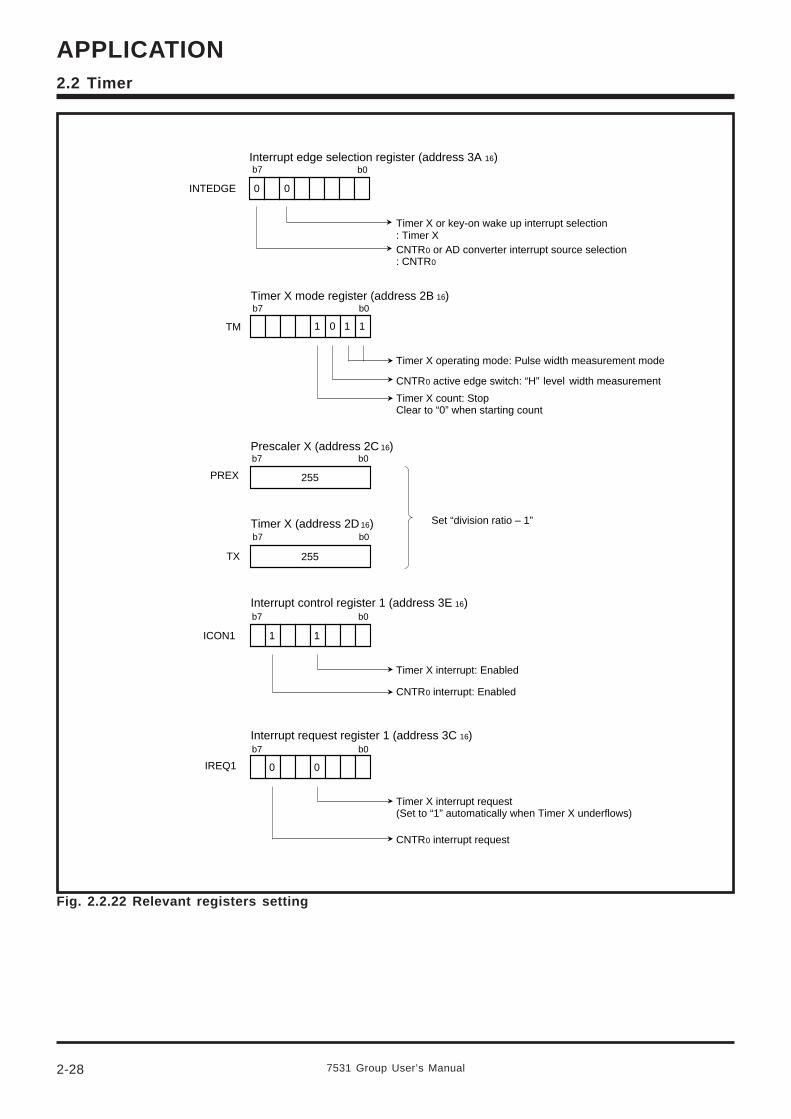
7531 Group User’s Manual2-28
APPLICATION2.2 Timer
Fig. 2.2.22 Relevant registers setting
TM
PREX 255
TX
0 11 1
255
ICON1
IREQ1
1
0
b0b7
b0b7
b0b7
b0b7
b0b7
INTEDGE 0
b0b7
0
1
0
Timer X interrupt: Enabled
Timer X mode register (address 2B 16)
Timer X operating mode: Pulse width measurement mode
Timer X count: StopClear to “0” when starting count
Prescaler X (address 2C 16)
Timer X (address 2D 16) Set “division ratio – 1”
Interrupt control register 1 (address 3E 16)
CNTR0 active edge switch: “H” level width measurement
Timer X or key-on wake up interrupt selection: Timer X
Interrupt edge selection register (address 3A 16)
CNTR0 interrupt: Enabled
Interrupt request register 1 (address 3C 16)
CNTR0 or AD converter interrupt source selection: CNTR0
Timer X interrupt request(Set to “1” automatically when Timer X underflows)
CNTR0 interrupt request
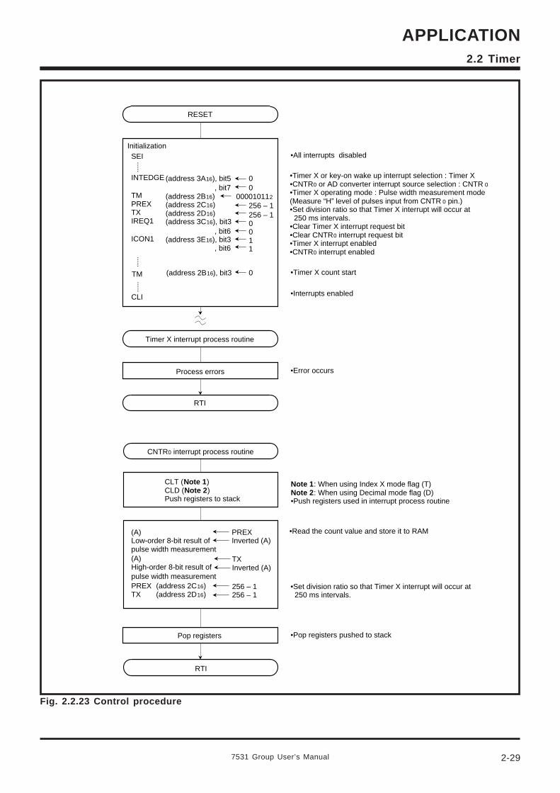
7531 Group User’s Manual
APPLICATION
2-29
2.2 Timer
Fig. 2.2.23 Control procedure
RESET
SEI
INTEDGE
TMPREXTXIREQ1
ICON1
TM
CLI
00
..........
0
.....
RTI
RTI
(address 3A16), bit5, bit7
(address 2B16)(address 2C16)(address 2D16)(address 3C16), bit3
, bit6(address 3E16), bit3
, bit6
PREXInverted (A)
(A)Low-order 8-bit result of pulse width measurement(A)High-order 8-bit result of pulse width measurementPREX (address 2C16)TX (address 2D16)
(address 2B16), bit3
256 – 1256 – 10011
000010112
TXInverted (A)
256 – 1256 – 1
•All interrupts disabled
•Timer X or key-on wake up interrupt selection : Timer X•CNTR0 or AD converter interrupt source selection : CNTR 0
•Timer X operating mode : Pulse width measurement mode(Measure “H” level of pulses input from CNTR 0 pin.)•Set division ratio so that Timer X interrupt will occur at250 ms intervals.
•Clear Timer X interrupt request bit•Clear CNTR0 interrupt request bit•Timer X interrupt enabled•CNTR0 interrupt enabled
•Timer X count start
•Interrupts enabled
Note 1: When using Index X mode flag (T)Note 2: When using Decimal mode flag (D)•Push registers used in interrupt process routine
•Pop registers pushed to stackPop registers
Initialization
Timer X interrupt process routine
CLT (Note 1)CLD (Note 2)Push registers to stack
Process errors •Error occurs
CNTR0 interrupt process routine
•Set division ratio so that Timer X interrupt will occur at250 ms intervals.
•Read the count value and store it to RAM
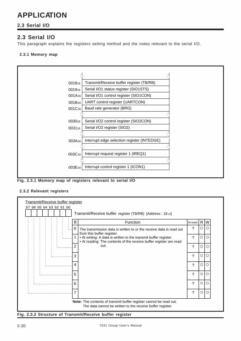
7531 Group User’s Manual2-30
APPLICATION2.3 Serial I/O
2.3 Serial I/OThis paragraph explains the registers setting method and the notes relevant to the serial I/O.
2.3.1 Memory map
Fig. 2.3.1 Memory map of registers relevant to serial I/O
2.3.2 Relevant registers
Fig. 2.3.2 Structure of Transmit/Receive buffer register
001816
001916
001A16
001B16
001C16
003A16
003C16
Transmit/Receive buffer register (TB/RB)
Serial I/O1 status register (SIO1STS)
Serial I/O1 control register (SIO1CON)
UART control register (UARTCON)
Baud rate generator (BRG)
Interrupt edge selection register (INTEDGE)
Interrupt request register 1 (IREQ1)
003E16 Interrupt control register 1 (ICON1)
003016 Serial I/O2 control register (SIO2CON)
003116 Serial I/O2 register (SIO2)
Transmit/Receive buffer registerb7 b6 b5 b4 b3 b2 b1 b0
B Function At reset R W
0
1
2
3
4
5
6
7
?
?
?
?
?
?
?
?
Transmit/Receive buffer register (TB/RB) [Address : 18 16]
The transmission data is written to or the receive data is read out from this buffer register.• At writing: A data is written to the transmit buffer register.• At reading: The contents of the receive buffer register are read
out.
Note: The contents of transmit buffer register cannot be read out.The data cannot be written to the receive buffer register.
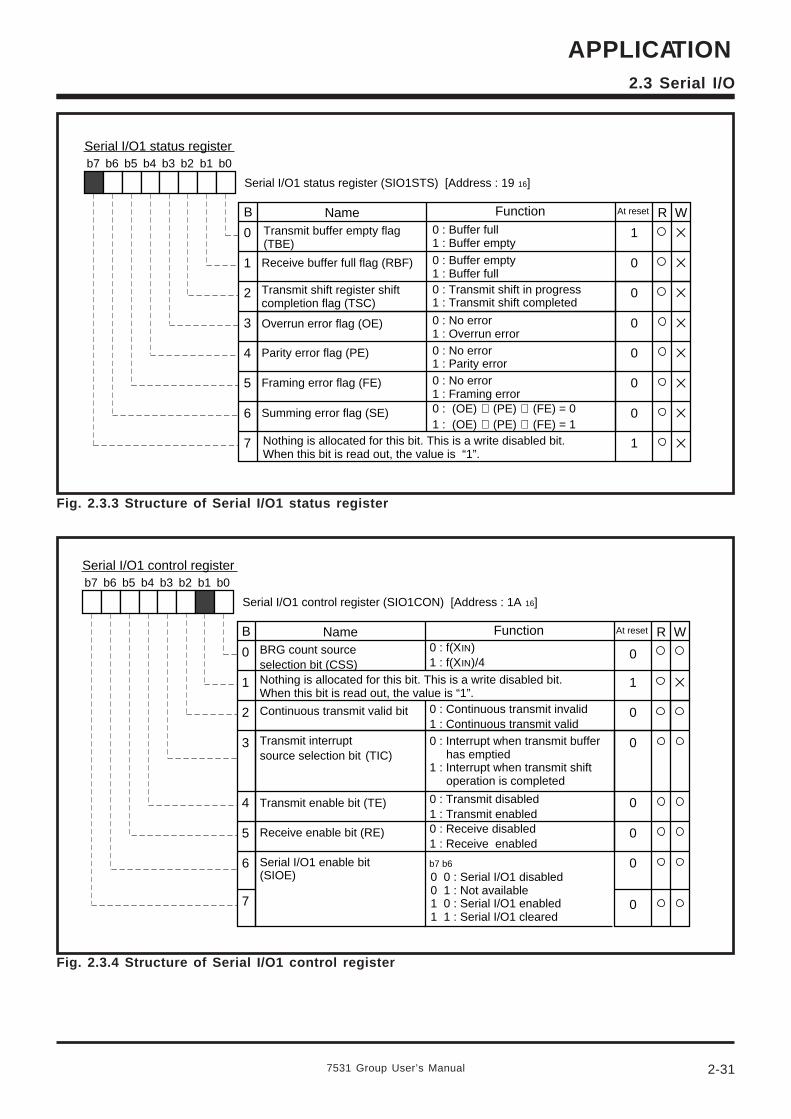
7531 Group User’s Manual
APPLICATION
2-31
2.3 Serial I/O
Fig. 2.3.3 Structure of Serial I/O1 status register
Fig. 2.3.4 Structure of Serial I/O1 control register
Serial I/O1 status registerb7 b6 b5 b4 b3 b2 b1 b0
B Function At reset R W
0
1
2
3
4
5
6
7
Name
1
0
0
0
0
0
0
1
Serial I/O1 status register (SIO1STS) [Address : 19 16]
Nothing is allocated for this bit. This is a write disabled bit.When this bit is read out, the value is “1”.
Transmit buffer empty flag (TBE)
0 : (OE) ∪ (PE) ∪ (FE) = 01 : (OE) ∪ (PE) ∪ (FE) = 1
Overrun error flag (OE)
0 : Buffer full1 : Buffer empty
Receive buffer full flag (RBF)
Transmit shift register shift completion flag (TSC)
Parity error flag (PE)
Framing error flag (FE)
Summing error flag (SE)
0 : Buffer empty1 : Buffer full0 : Transmit shift in progress1 : Transmit shift completed
0 : No error1 : Overrun error0 : No error1 : Parity error0 : No error1 : Framing error
Serial I/O1 control registerb7 b6 b5 b4 b3 b2 b1 b0
B Function At reset R W
0
1
2
3
4
5
6
7
Name
1
0
0
0
0
0
0
Serial I/O1 control register (SIO1CON) [Address : 1A 16]
Nothing is allocated for this bit. This is a write disabled bit.When this bit is read out, the value is “1”.
0 : f(XIN)1 : f(XIN)/4
BRG count source selection bit (CSS)
0
0 : Transmit disabled1 : Transmit enabled0 : Receive disabled1 : Receive enabled
Transmit interrupt source selection bit (TIC)
Transmit enable bit (TE)
Receive enable bit (RE)
Serial I/O1 enable bit(SIOE)
Continuous transmit valid bit 0 : Continuous transmit invalid1 : Continuous transmit valid0 : Interrupt when transmit buffer
has emptied1 : Interrupt when transmit shift
operation is completed
0 0 : Serial I/O1 disabled0 1 : Not available1 0 : Serial I/O1 enabled1 1 : Serial I/O1 cleared
b7 b6
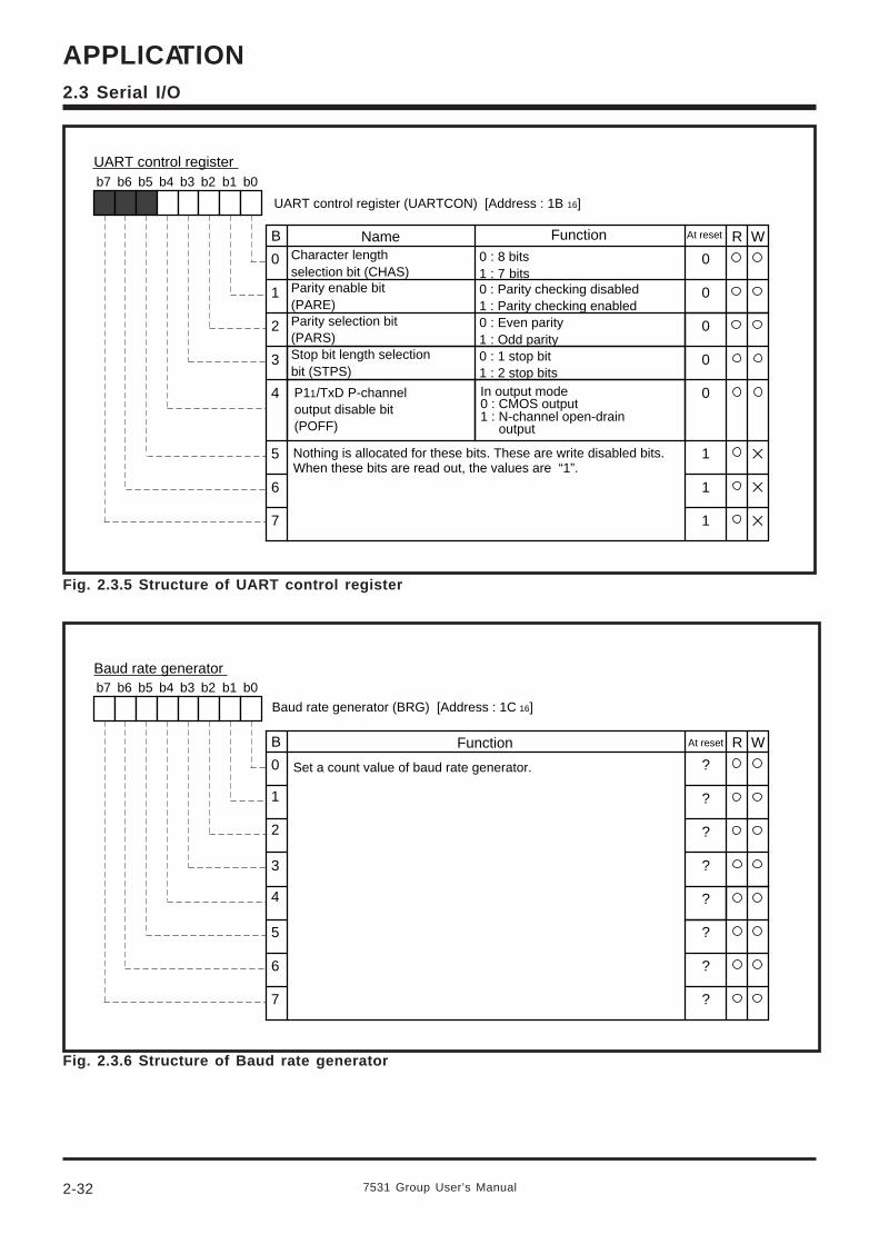
7531 Group User’s Manual2-32
APPLICATION2.3 Serial I/O
Fig. 2.3.5 Structure of UART control register
b7 b6 b5 b4 b3 b2 b1 b0
B Function At reset R W
0
1
2
3
4
5
6
7
Name
0
0
0
0
1
UART control register (UARTCON) [Address : 1B 16]
Nothing is allocated for these bits. These are write disabled bits.When these bits are read out, the values are “1”.
UART control register
Character length selection bit (CHAS)Parity enable bit(PARE)
Stop bit length selectionbit (STPS)
Parity selection bit(PARS)
In output mode0 : CMOS output1 : N-channel open-drain output
0 : 8 bits1 : 7 bits0 : Parity checking disabled1 : Parity checking enabled
0 : 1 stop bit1 : 2 stop bits
0 : Even parity1 : Odd parity
P11/TxD P-channel output disable bit(POFF)
1
1
0
Fig. 2.3.6 Structure of Baud rate generator
Baud rate generatorb7 b6 b5 b4 b3 b2 b1 b0
B Function At reset R W
0
1
2
3
4
5
6
7
?
?
?
?
?
?
?
?
Baud rate generator (BRG) [Address : 1C 16]
Set a count value of baud rate generator.
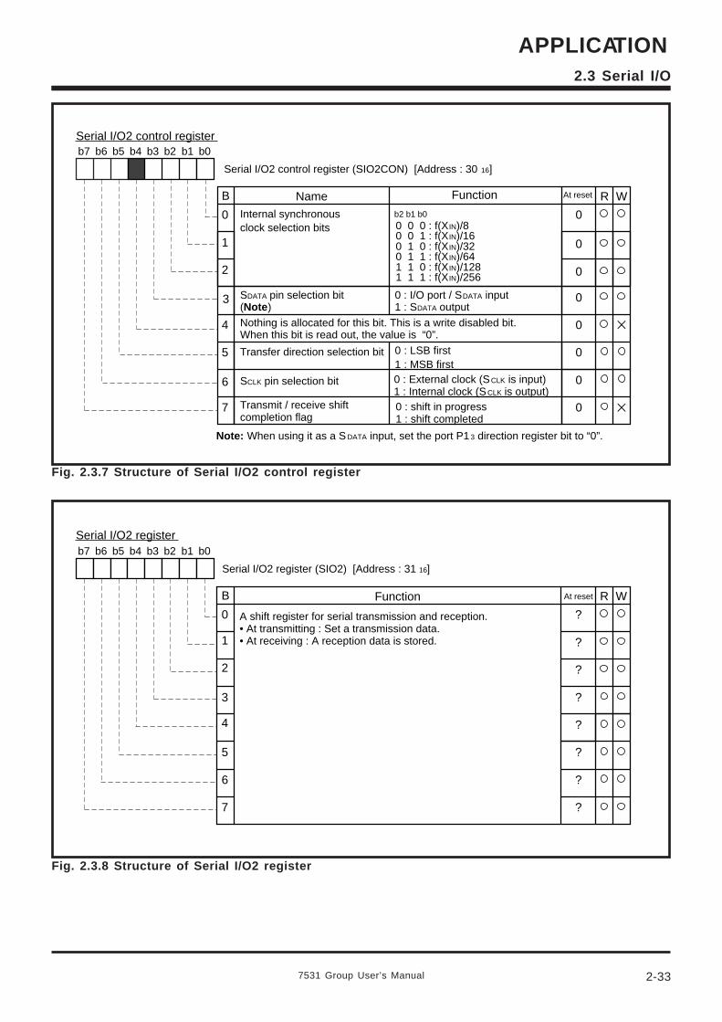
7531 Group User’s Manual
APPLICATION
2-33
2.3 Serial I/O
Fig. 2.3.7 Structure of Serial I/O2 control register
b7 b6 b5 b4 b3 b2 b1 b0
B Function At reset R W
0
1
2
3
4
5
6
7
Name
0
0
0
0
Serial I/O2 control register (SIO2CON) [Address : 30 16]
Nothing is allocated for this bit. This is a write disabled bit.When this bit is read out, the value is “0”.
Serial I/O2 control register
0
0
Note: When using it as a S DATA input, set the port P13 direction register bit to “0”.
0 : LSB first1 : MSB first
0 0 0 : f(XIN)/80 0 1 : f(XIN)/160 1 0 : f(XIN)/320 1 1 : f(XIN)/641 1 0 : f(XIN)/1281 1 1 : f(XIN)/256
Internal synchronous clock selection bits
Transfer direction selection bit
b2 b1 b0
SDATA pin selection bit(Note)
0 : I/O port / SDATA input1 : SDATA output
SCLK pin selection bit 0 : External clock (SCLK is input)1 : Internal clock (S CLK is output)
Transmit / receive shift completion flag
0 : shift in progress1 : shift completed
0
0
Serial I/O2 registerb7 b6 b5 b4 b3 b2 b1 b0
B Function At reset R W
0
1
2
3
4
5
6
7
?
?
?
?
?
?
?
?
Serial I/O2 register (SIO2) [Address : 31 16]
A shift register for serial transmission and reception.• At transmitting : Set a transmission data.• At receiving : A reception data is stored.
Fig. 2.3.8 Structure of Serial I/O2 register
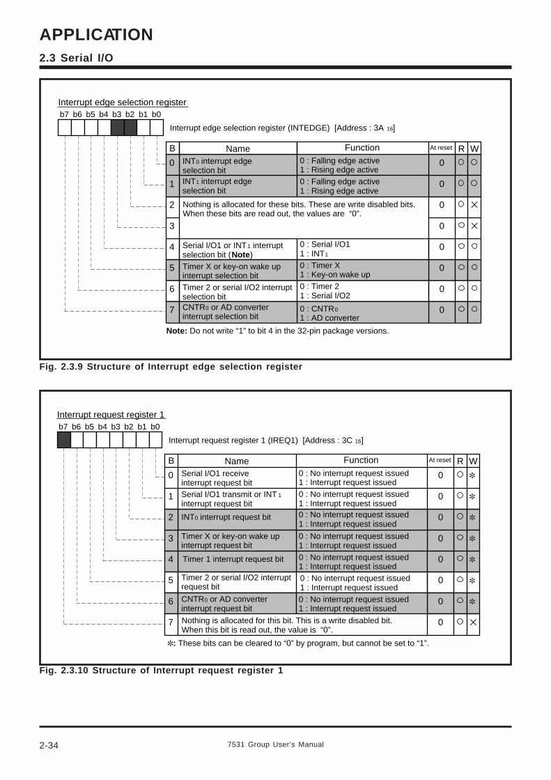
7531 Group User’s Manual2-34
APPLICATION2.3 Serial I/O
Fig. 2.3.9 Structure of Interrupt edge selection register
Fig. 2.3.10 Structure of Interrupt request register 1
Interrupt request register 1b7 b6 b5 b4 b3 b2 b1 b0
B Function At reset R W
0
1
2
3
4
5
6
7
Name
0
0
0
0
0
0
0
0
Interrupt request register 1 (IREQ1) [Address : 3C 16]
Nothing is allocated for this bit. This is a write disabled bit.When this bit is read out, the value is “0”.
Serial I/O1 receive interrupt request bitSerial I/O1 transmit or INT 1 interrupt request bit
0 : No interrupt request issued1 : Interrupt request issued
Timer 2 or serial I/O2 interrupt request bit
CNTR0 or AD converter interrupt request bit
: These bits can be cleared to “0” by program, but cannot be set to “1”.
0 : No interrupt request issued1 : Interrupt request issued
INT0 interrupt request bit
Timer X or key-on wake up interrupt request bit
0 : No interrupt request issued1 : Interrupt request issued
0 : No interrupt request issued1 : Interrupt request issued
Timer 1 interrupt request bit 0 : No interrupt request issued1 : Interrupt request issued0 : No interrupt request issued1 : Interrupt request issued0 : No interrupt request issued1 : Interrupt request issued
Interrupt edge selection registerb7 b6 b5 b4 b3 b2 b1 b0
B Function At reset R W
0
1
2
3
4
5
6
7
Name
0
0
0
0
0
0
0
0
Interrupt edge selection register (INTEDGE) [Address : 3A 16]
Nothing is allocated for these bits. These are write disabled bits.When these bits are read out, the values are “0”.
INT0 interrupt edge selection bitINT1 interrupt edge selection bit
0 : Falling edge active1 : Rising edge active0 : Falling edge active1 : Rising edge active
Serial I/O1 or INT1 interrupt selection bit (Note)Timer X or key-on wake up interrupt selection bitTimer 2 or serial I/O2 interrupt selection bitCNTR0 or AD converter interrupt selection bit
0 : Serial I/O11 : INT1
0 : Timer X1 : Key-on wake up0 : Timer 21 : Serial I/O2
0 : CNTR0
1 : AD converter
Note: Do not write “1” to bit 4 in the 32-pin package versions.
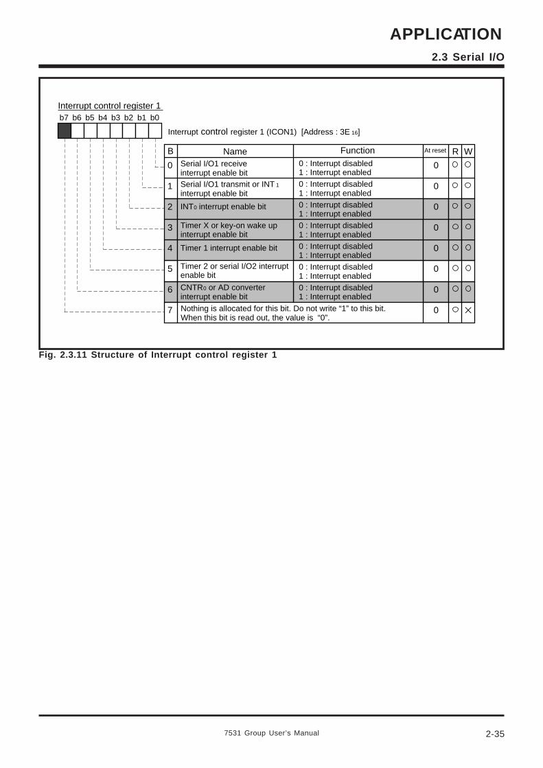
7531 Group User’s Manual
APPLICATION
2-35
2.3 Serial I/O
Fig. 2.3.11 Structure of Interrupt control register 1
Interrupt control register 1b7 b6 b5 b4 b3 b2 b1 b0
B Function At reset R W
0
1
2
3
4
5
6
7
Name
0
0
0
0
0
0
0
0
Interrupt control register 1 (ICON1) [Address : 3E 16]
Nothing is allocated for this bit. Do not write “1” to this bit.When this bit is read out, the value is “0”.
Serial I/O1 receive interrupt enable bitSerial I/O1 transmit or INT 1 interrupt enable bit
0 : Interrupt disabled1 : Interrupt enabled
Timer 2 or serial I/O2 interrupt enable bit
CNTR0 or AD converter interrupt enable bit
INT0 interrupt enable bit
Timer X or key-on wake up interrupt enable bit
Timer 1 interrupt enable bit
0 : Interrupt disabled1 : Interrupt enabled0 : Interrupt disabled1 : Interrupt enabled0 : Interrupt disabled1 : Interrupt enabled0 : Interrupt disabled1 : Interrupt enabled0 : Interrupt disabled1 : Interrupt enabled0 : Interrupt disabled1 : Interrupt enabled
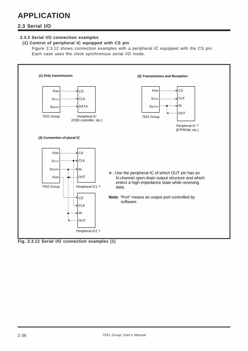
7531 Group User’s Manual2-36
APPLICATION2.3 Serial I/O
2.3.3 Serial I/O connection examples(1) Control of peripheral IC equipped with CS pin
Figure 2.3.12 shows connection examples with a peripheral IC equipped with the CS pin.Each case uses the clock synchronous serial I/O mode.
Port
SCLK
SDATA
CS
CLK
DATA
(1) Only transmission
Peripheral IC(OSD controller, etc.)
7531 Group
(2) Transmission and Reception
Port
SCLK
SDATA
CS
CLK
IN
OUT7531 Group
Port
SCLK
SDATA
Port
(3) Connection of plural IC
CS
CLK
CS
CLK
IN
OUT
Peripheral IC
(E2PROM, etc.)
7531 Group Peripheral IC1
IN
OUT
Peripheral IC2
: Use the peripheral IC of which OUT pin has an N-channel open-drain output structure and which enters a high-impedance state while receiving data.
Note: “Port” means an output port controlled by software.
Fig. 2.3.12 Serial I/O connection examples (1)
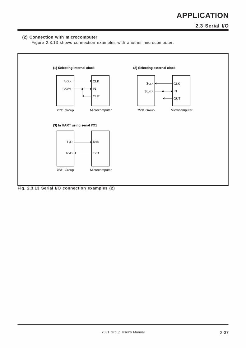
7531 Group User’s Manual
APPLICATION
2-37
2.3 Serial I/O
SCLK
SDATA
CLK
IN
OUT
(1) Selecting internal clock
SCLK
SDATA
CLK
IN
OUT
7531 Group Microcomputer
TXD
RXD
RXD
TXD
(2) Selecting external clock
7531 Group Microcomputer
(3) In UART using serial I/O1
7531 Group Microcomputer
Fig. 2.3.13 Serial I/O connection examples (2)
(2) Connection with microcomputerFigure 2.3.13 shows connection examples with another microcomputer.
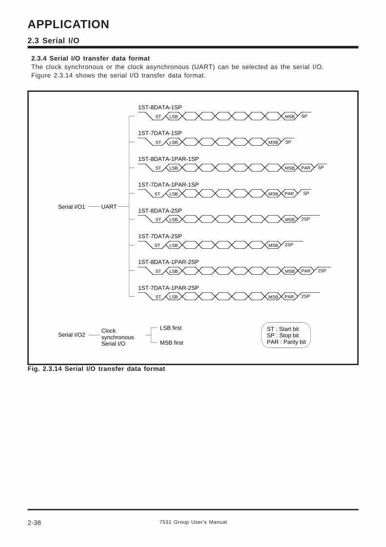
7531 Group User’s Manual2-38
APPLICATION2.3 Serial I/O
2.3.4 Serial I/O transfer data formatThe clock synchronous or the clock asynchronous (UART) can be selected as the serial I/O.Figure 2.3.14 shows the serial I/O transfer data format.
1ST-8DATA-1SP
ST LSB
Serial I/O1 UART
Clock synchronousSerial I/O
1ST-7DATA-1SP
ST LSB
1ST-8DATA-1PAR-1SP
ST LSB
1ST-7DATA-1PAR-1SP
ST LSB
1ST-8DATA-2SP
ST LSB
1ST-7DATA-2SP
ST LSB
1ST-8DATA-1PAR-2SP
ST LSB
1ST-7DATA-1PAR-2SP
ST LSB
MSB SP
MSB SP
MSB PAR SP
MSB PAR SP
MSB 2SP
MSB 2SP
MSB PAR 2SP
MSB PAR 2SP
LSB first ST : Start bitSP : Stop bitPAR : Parity bit
Serial I/O2MSB first
Fig. 2.3.14 Serial I/O transfer data format
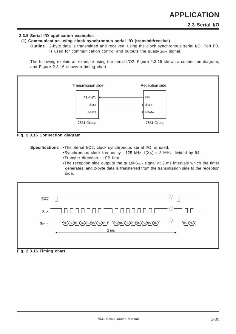
7531 Group User’s Manual
APPLICATION
2-39
2.3 Serial I/O
2.3.5 Serial I/O application examples(1) Communication using clock synchronous serial I/O (transmit/receive)
Outline : 2-byte data is transmitted and received, using the clock synchronous serial I/O. Port P00
is used for communication control and outputs the quasi-SRDY signal.
The following explain an example using the serial I/O2. Figure 2.3.15 shows a connection diagram,and Figure 2.3.16 shows a timing chart.
Transmission side
P37/INT0
SCLK
SDATA
7531 Group
P00
SCLK
SDATA
Reception side
7531 Group
Fig. 2.3.15 Connection diagram
Specifications : •The Serial I/O2, clock synchronous serial I/O, is used.•Synchronous clock frequency : 125 kHz; f(XIN) = 8 MHz divided by 64•Transfer direction : LSB first•The reception side outputs the quasi-SRDY signal at 2 ms intervals which the timer
generates, and 2-byte data is transferred from the transmission side to the receptionside.
SRDY
D0 D1 D2 D3 D4 D5 D6 D7 D0 D1 D2 D3 D4 D5 D6 D7 D0 D1
2 ms
@ @ @
@ @ @
@ @ @SDATA
SCLK
Fig. 2.3.16 Timing chart
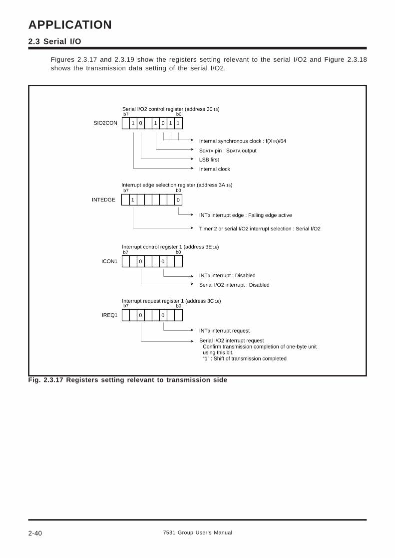
7531 Group User’s Manual2-40
APPLICATION2.3 Serial I/O
Figures 2.3.17 and 2.3.19 show the registers setting relevant to the serial I/O2 and Figure 2.3.18shows the transmission data setting of the serial I/O2.
Interrupt control register 1 (address 3E 16)
ICON1
Serial I/O2 interrupt : Disabled
0
Interrupt request register 1 (address 3C 16)
IREQ1
Serial I/O2 interrupt requestConfirm transmission completion of one-byte unit using this bit.“1” : Shift of transmission completed
0
Serial I/O2 control register (address 30 16)
SIO2CON
Internal synchronous clock : f(X IN)/64
SDATA pin : SDATA output
LSB first
Internal clock
00 11 11
b0b7
b0b7
b0b7
Interrupt edge selection register (address 3A 16)
INTEDGE 1
b0b7
0
INT0 interrupt edge : Falling edge active
0
INT0 interrupt : Disabled
0
INT0 interrupt request
Timer 2 or serial I/O2 interrupt selection : Serial I/O2
Fig. 2.3.17 Registers setting relevant to transmission side
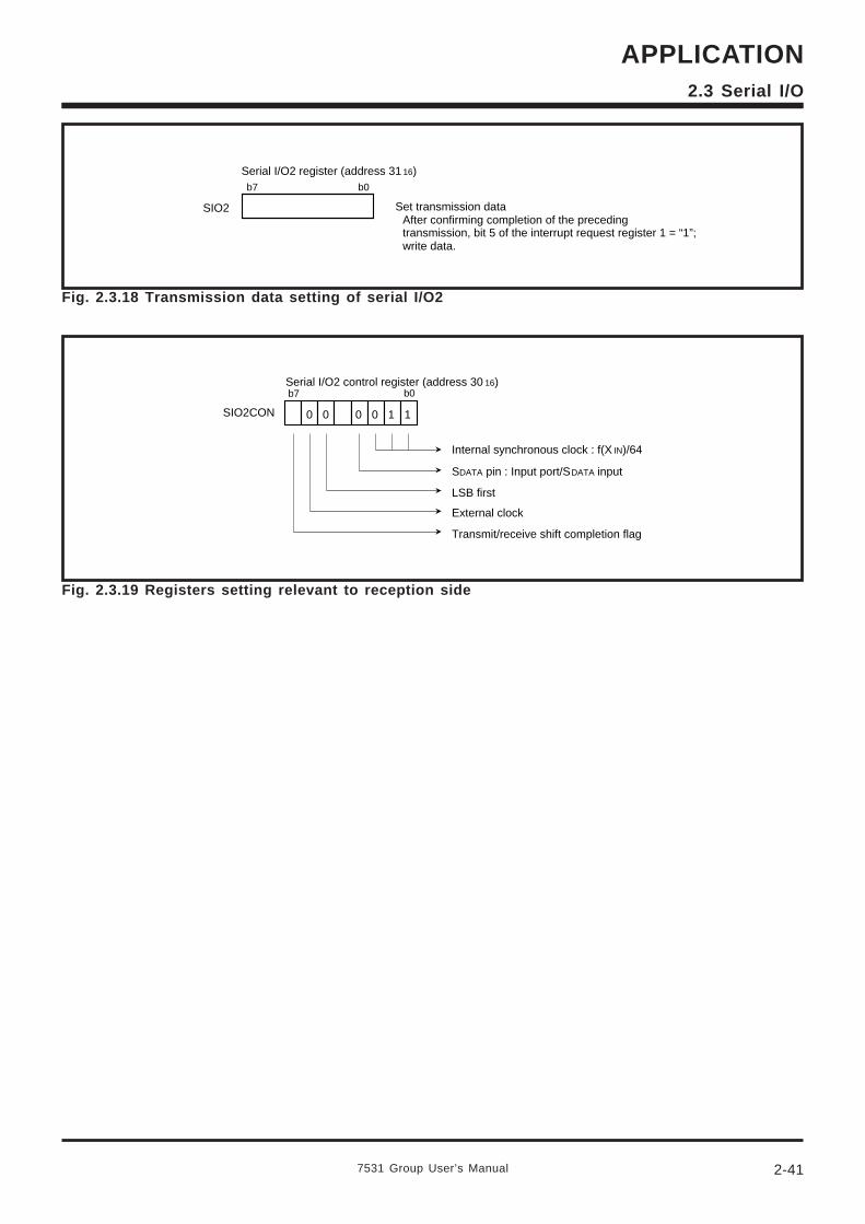
7531 Group User’s Manual
APPLICATION
2-41
2.3 Serial I/O
Fig. 2.3.18 Transmission data setting of serial I/O2
SIO2
b7 b0
Serial I/O2 register (address 31 16)
Set transmission dataAfter confirming completion of the preceding transmission, bit 5 of the interrupt request register 1 = “1”;write data.
Fig. 2.3.19 Registers setting relevant to reception side
Serial I/O2 control register (address 30 16)
SIO2CON
Internal synchronous clock : f(X IN)/64
LSB first
External clock
00 10 10
Transmit/receive shift completion flag
b0b7
SDATA pin : Input port/SDATA input
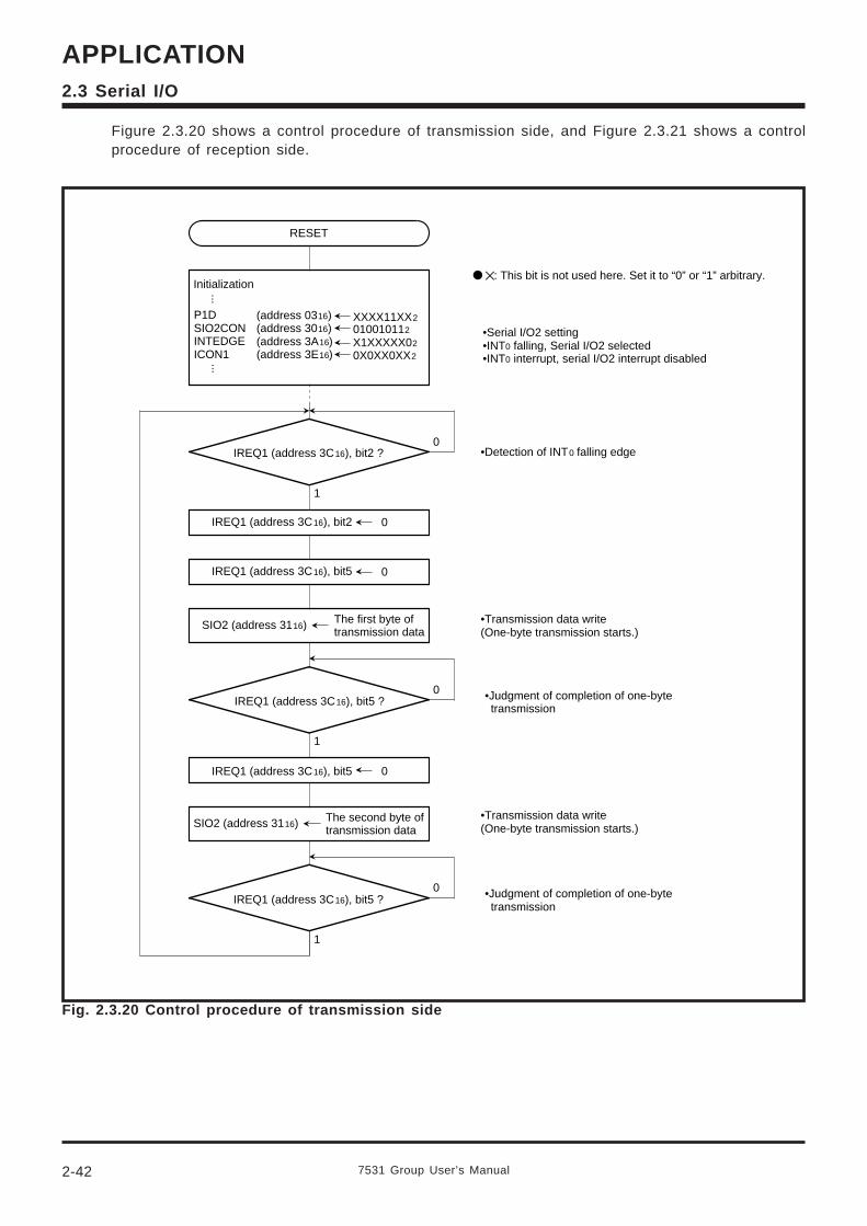
7531 Group User’s Manual2-42
APPLICATION2.3 Serial I/O
RESET
XXXX11XX2
...
SIO2 (address 3116) The first byte of transmission data
IREQ1 (address 3C16), bit2 ?
1
0
P1DSIO2CONINTEDGEICON1
IREQ1 (address 3C16), bit2 0
(address 0316)(address 3016)(address 3A16)(address 3E16)...
IREQ1 (address 3C16), bit5 0
IREQ1 (address 3C16), bit5 ?
1
0
SIO2 (address 3116)
IREQ1 (address 3C16), bit5 0
IREQ1 (address 3C16), bit5 ?
1
0
: This bit is not used here. Set it to “0” or “1” arbitrary.Initialization
010010112
X1XXXXX02
0X0XX0XX2
The second byte of transmission data
•Serial I/O2 setting•INT0 falling, Serial I/O2 selected•INT0 interrupt, serial I/O2 interrupt disabled
•Detection of INT0 falling edge
•Transmission data write(One-byte transmission starts.)
•Judgment of completion of one-byte transmission
•Transmission data write(One-byte transmission starts.)
•Judgment of completion of one-byte transmission
Fig. 2.3.20 Control procedure of transmission side
Figure 2.3.20 shows a control procedure of transmission side, and Figure 2.3.21 shows a controlprocedure of reception side.
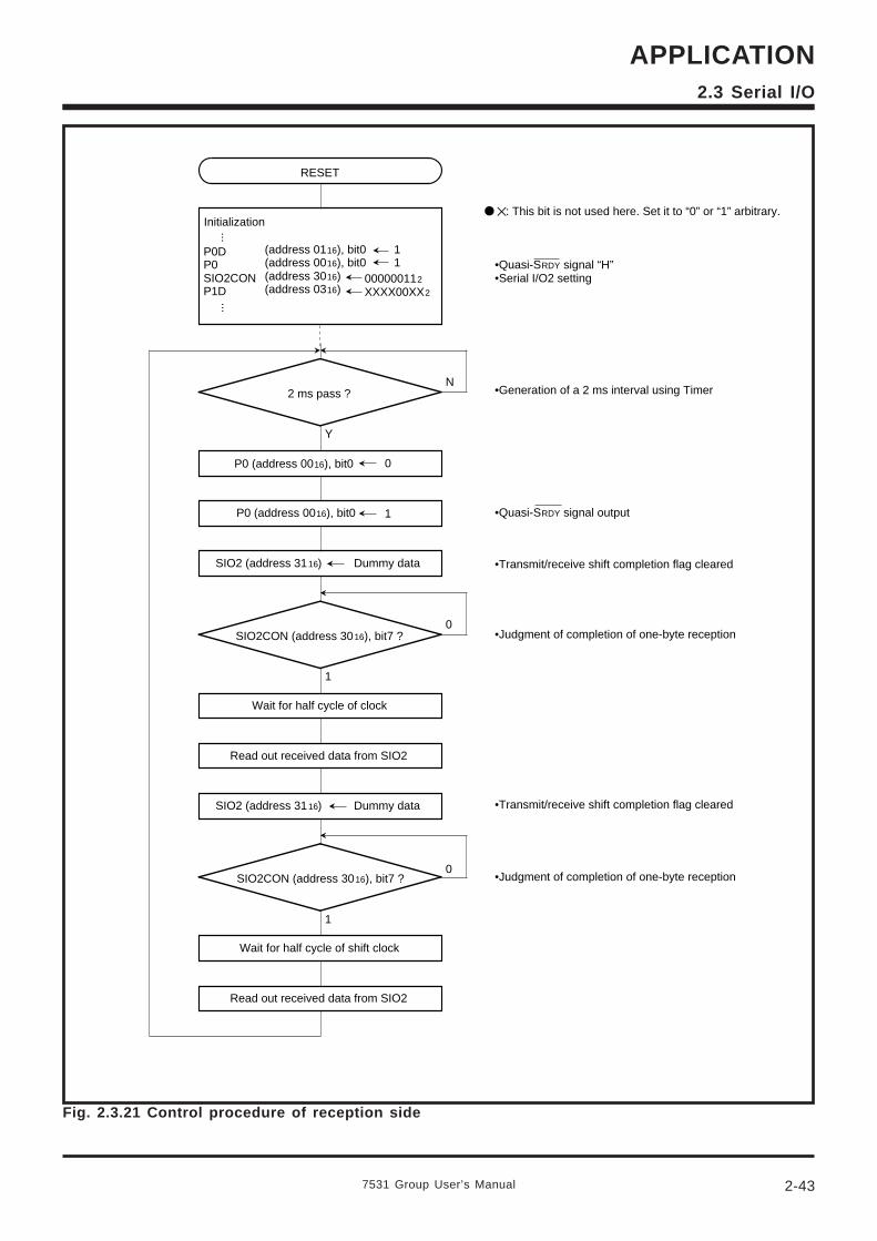
7531 Group User’s Manual
APPLICATION
2-43
2.3 Serial I/O
Fig. 2.3.21 Control procedure of reception side
RESET
000000112
XXXX00XX2
...
SIO2 (address 3116)
2 ms pass ?
Y
N
P0DP0SIO2CONP1D
P0 (address 0016), bit0 0
(address 0116), bit0(address 0016), bit0(address 3016)(address 0316)
...
P0 (address 0016), bit0 1
SIO2CON (address 3016), bit7 ?
1
0
SIO2CON (address 3016), bit7 ?
1
0
Wait for half cycle of clock
: This bit is not used here. Set it to “0” or “1” arbitrary.
•Quasi-SRDY signal “H”•Serial I/O2 setting
•Judgment of completion of one-byte reception
Initialization
11
Dummy data
Read out received data from SIO2
SIO2 (address 3116) Dummy data
Wait for half cycle of shift clock
Read out received data from SIO2
•Generation of a 2 ms interval using Timer
•Quasi-SRDY signal output
•Transmit/receive shift completion flag cleared
•Transmit/receive shift completion flag cleared
•Judgment of completion of one-byte reception
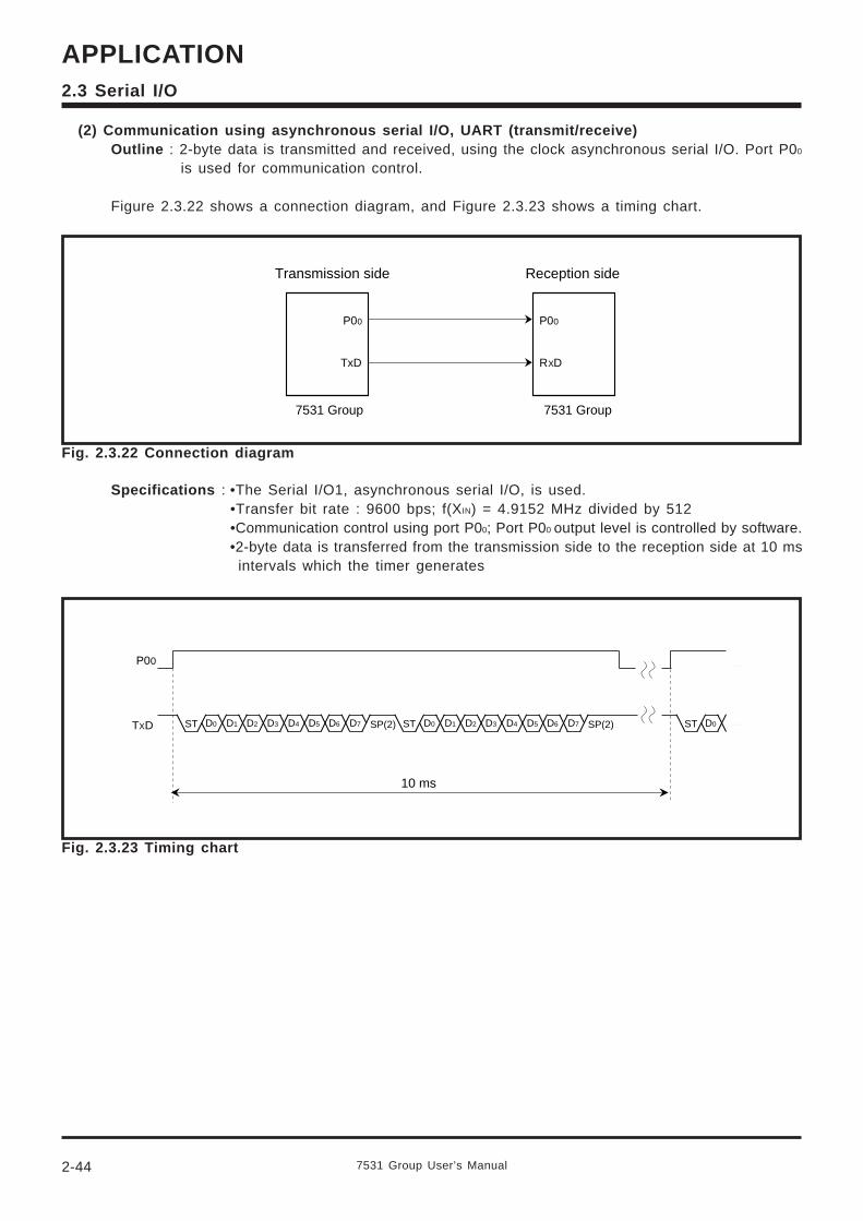
7531 Group User’s Manual2-44
APPLICATION2.3 Serial I/O
(2) Communication using asynchronous serial I/O, UART (transmit/receive)Outline : 2-byte data is transmitted and received, using the clock asynchronous serial I/O. Port P00
is used for communication control.
Figure 2.3.22 shows a connection diagram, and Figure 2.3.23 shows a timing chart.
Fig. 2.3.22 Connection diagram
Specifications : •The Serial I/O1, asynchronous serial I/O, is used.•Transfer bit rate : 9600 bps; f(XIN) = 4.9152 MHz divided by 512•Communication control using port P00; Port P00 output level is controlled by software.•2-byte data is transferred from the transmission side to the reception side at 10 ms
intervals which the timer generates
Fig. 2.3.23 Timing chart
P00
TxD
P00
RXD
Transmission side
7531 Group
Reception side
7531 Group
P00
10 ms
D0 D1 D2 D3 D4 D5 D6 D7ST SP(2) D0 D1 D2 D3 D4 D5 D6 D7ST SP(2) D0ST
@ @ @
@ @ @TXD
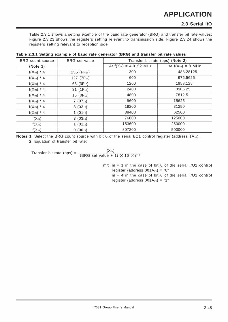
7531 Group User’s Manual
APPLICATION
2-45
2.3 Serial I/O
Table 2.3.1 shows a setting example of the baud rate generator (BRG) and transfer bit rate values;Figure 2.3.23 shows the registers setting relevant to transmission side; Figure 2.3.24 shows theregisters setting relevant to reception side
Table 2.3.1 Setting example of baud rate generator (BRG) and transfer bit rate values
BRG count source
(Note 1 )
f(XIN) / 4
f(XIN) / 4
f(XIN) / 4
f(XIN) / 4
f(XIN) / 4
f(XIN) / 4
f(XIN) / 4
f(XIN) / 4
f(XIN)
f(XIN)
f(XIN)
BRG set value
255 (FF16)
127 (7F16)
63 (3F16)
31 (1F16)
15 (0F16)
7 (0716)
3 (0316)
1 (0116)
3 (0316)
1 (0116)
0 (0016)
Transfer bit rate (bps) (Note 2 )At f(XIN) = 4.9152 MHz
300
600
1200
2400
4800
9600
19200
38400
76800
153600
307200
At f(XIN) = 8 MHz
488.28125
976.5625
1953.125
3906.25
7812.5
15625
31250
62500
125000
250000
500000
Notes 1 : Select the BRG count source with bit 0 of the serial I/O1 control register (address 1A16).2: Equation of transfer bit rate:
Transfer bit rate (bps) =f(XIN)
(BRG set value + 1) 16 m
m: m = 1 in the case of bit 0 of the serial I/O1 controlregister (address 001A16) = “0”m = 4 in the case of bit 0 of the serial I/O1 controlregister (address 001A16) = “1”
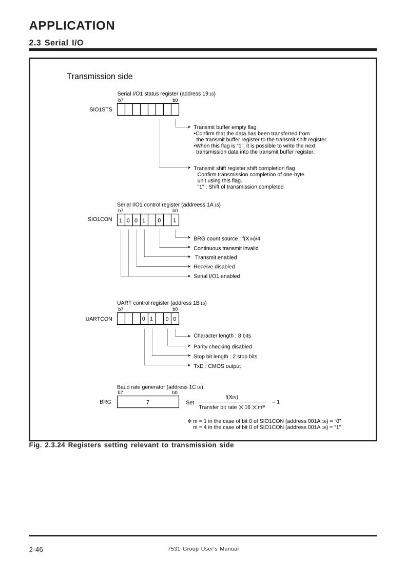
7531 Group User’s Manual2-46
APPLICATION2.3 Serial I/O
Fig. 2.3.24 Registers setting relevant to transmission side
Serial I/O1 status register (address 19 16)
SIO1STS
Transmission side
Baud rate generator (address 1C 16)
BRG 7
Serial I/O1 control register (addreess 1A 16)
SIO1CON
BRG count source : f(X IN)/4
1 0 1 10
UART control register (address 1B 16)
UARTCON 00 1 0
f(XIN)
b0b7
b0b7
b0b7
b0b7
0
Transmit buffer empty flag•Confirm that the data has been transferred from the transmit buffer register to the transmit shift register.
•When this flag is “1”, it is possible to write the nexttransmission data into the transmit buffer register.
Transmit shift register shift completion flagConfirm transmission completion of one-byte unit using this flag.“1” : Shift of transmission completed
Continuous transmit invalid
Transmit enabled
Receive disabled
Serial I/O1 enabled
Character length : 8 bits
Parity checking disabled
Stop bit length : 2 stop bits
TxD : CMOS output
Transfer bit rate 16 m
m = 1 in the case of bit 0 of SIO1CON (address 001A 16) = “0”m = 4 in the case of bit 0 of SIO1CON (address 001A 16) = “1”
Set – 1
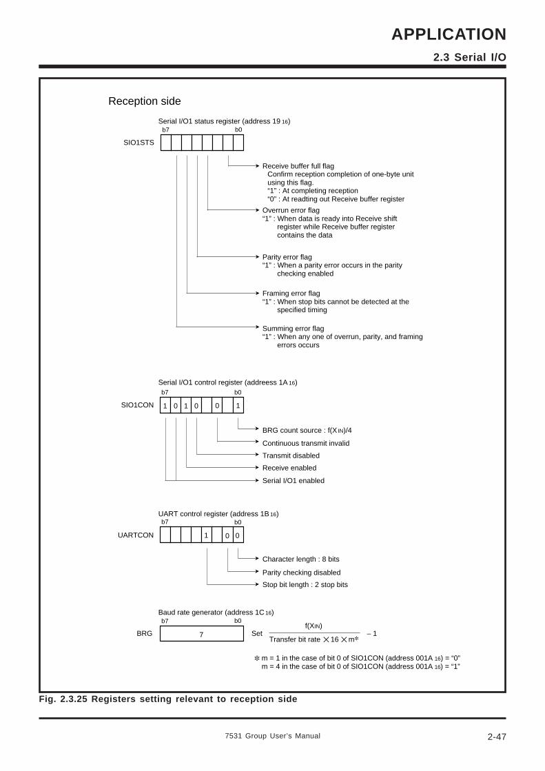
7531 Group User’s Manual
APPLICATION
2-47
2.3 Serial I/O
Fig. 2.3.25 Registers setting relevant to reception side
SIO1STS
BRG 7
SIO1CON 1 01 10
UARTCON 01 0
b0b7
b0b7
b0b7
b0b7
0
Reception side
Serial I/O1 status register (address 19 16)
Receive buffer full flagConfirm reception completion of one-byte unit using this flag.“1” : At completing reception“0” : At readting out Receive buffer register
Overrun error flag“1” : When data is ready into Receive shift
register while Receive buffer register contains the data
Parity error flag“1” : When a parity error occurs in the parity
checking enabled
Framing error flag“1” : When stop bits cannot be detected at the
specified timing
Summing error flag“1” : When any one of overrun, parity, and framing
errors occurs
Baud rate generator (address 1C 16)
Serial I/O1 control register (addreess 1A 16)
BRG count source : f(X IN)/4
UART control register (address 1B 16)
f(XIN)
Continuous transmit invalid
Transmit disabled
Receive enabled
Serial I/O1 enabled
Character length : 8 bits
Parity checking disabled
Stop bit length : 2 stop bits
Transfer bit rate 16 m
m = 1 in the case of bit 0 of SIO1CON (address 001A 16) = “0”m = 4 in the case of bit 0 of SIO1CON (address 001A 16) = “1”
Set – 1
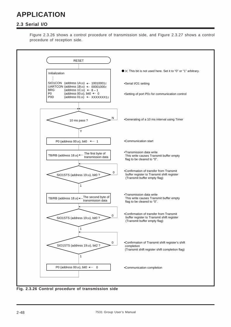
7531 Group User’s Manual2-48
APPLICATION2.3 Serial I/O
Fig. 2.3.26 Control procedure of transmission side
Figure 2.3.26 shows a control procedure of transmission side, and Figure 2.3.27 shows a controlprocedure of reception side.
RESET
P0 (address 0016), bit0 1
10 ms pass ?
Y
N
1
0
1
0
SIO1CONUARTCONBRGP0P0D
100100012
000010002
8 – 1
XXXXXXX12
.....
TB/RB (address 1816)
P0 (address 0016), bit0 0
SIO1STS (address 1916), bit0 ?
1
0
(address 1A16)(address 1B16)(address 1C16)(address 0016), bit0(address 0116)
: This bit is not used here. Set it to “0” or “1” arbitrary.Initialization
•Serial I/O1 setting
•Transmission data writeThis write causes Transmit buffer empty flag to be cleared to “0”.
0
The first byte of transmission data
TB/RB (address 1816) The second byte of transmission data
SIO1STS (address 1916), bit0 ?
SIO1STS (address 1916), bit2 ?
•Setting of port P00 for communication control
•Generating of a 10 ms interval using Timer
•Communication start
•Confirmation of transfer from Transmitbuffer register to Transmit shift register(Transmit buffer empty flag)
•Transmission data writeThis write causes Transmit buffer empty flag to be cleared to “0”.
•Confirmation of transfer from Transmitbuffer register to Transmit shift register(Transmit buffer empty flag)
•Confirmation of Transmit shift register’s shift completion(Transmit shift register shift completion flag)
•Communication completion
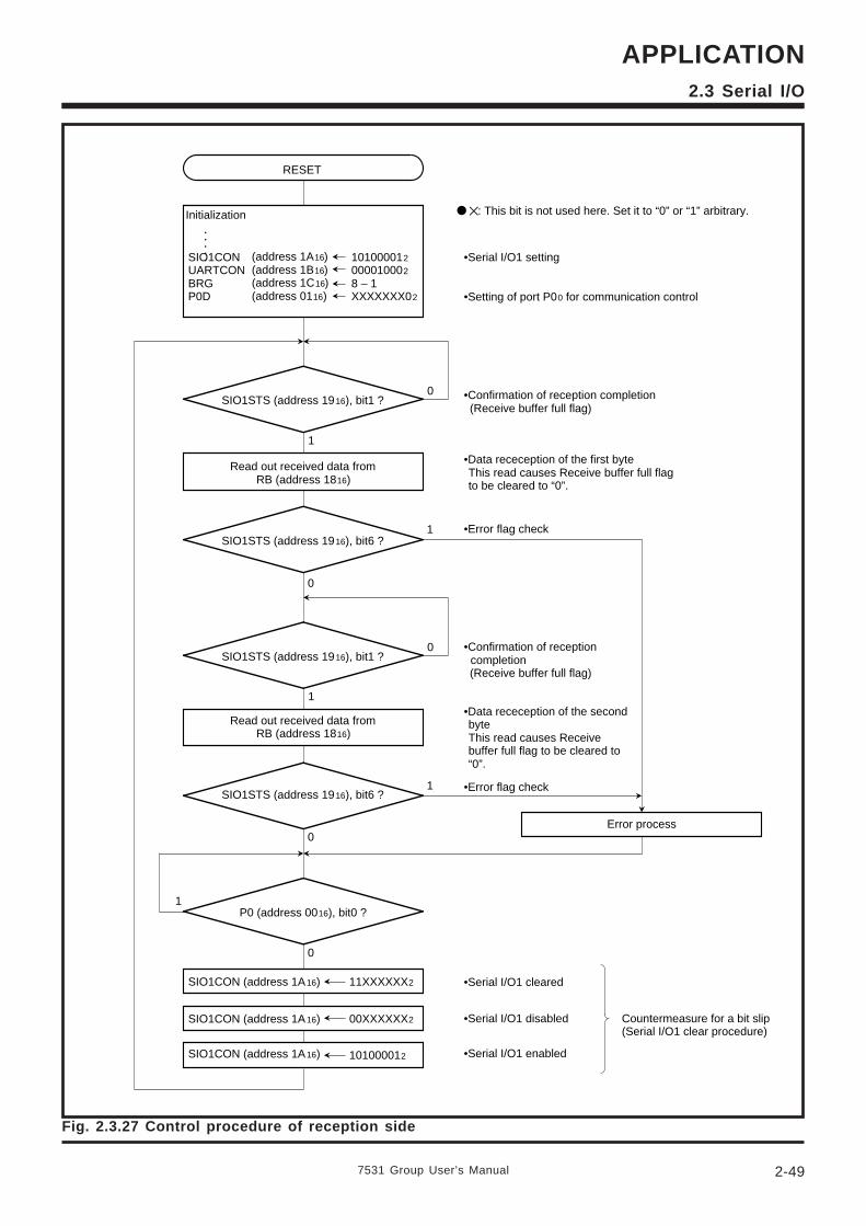
7531 Group User’s Manual
APPLICATION
2-49
2.3 Serial I/O
Fig. 2.3.27 Control procedure of reception side
RESET
SIO1STS (address 1916), bit1 ?
1
0
0
1
SIO1CONUARTCONBRGP0D
101000012
000010002
8 – 1XXXXXXX02
.....
1
0
0
1
P0 (address 0016), bit0 ?
0
1
SIO1CON (address 1A16) 11XXXXXX2
(address 1A16)(address 1B16)(address 1C16)(address 0116)
101000012
00XXXXXX2
: This bit is not used here. Set it to “0” or “1” arbitrary.Initialization
•Serial I/O1 setting
•Data receception of the first byteThis read causes Receive buffer full flag to be cleared to “0”.
•Setting of port P00 for communication control
Read out received data fromRB (address 1816)
SIO1STS (address 1916), bit6 ?
Read out received data fromRB (address 1816)
SIO1STS (address 1916), bit1 ?
SIO1STS (address 1916), bit6 ?
SIO1CON (address 1A16)
SIO1CON (address 1A16)
•Confirmation of reception completion(Receive buffer full flag)
•Error flag check
•Data receception of the second byteThis read causes Receive buffer full flag to be cleared to “0”.
•Confirmation of reception completion(Receive buffer full flag)
•Error flag check
Error process
•Serial I/O1 cleared
•Serial I/O1 disabled
•Serial I/O1 enabled
Countermeasure for a bit slip(Serial I/O1 clear procedure)
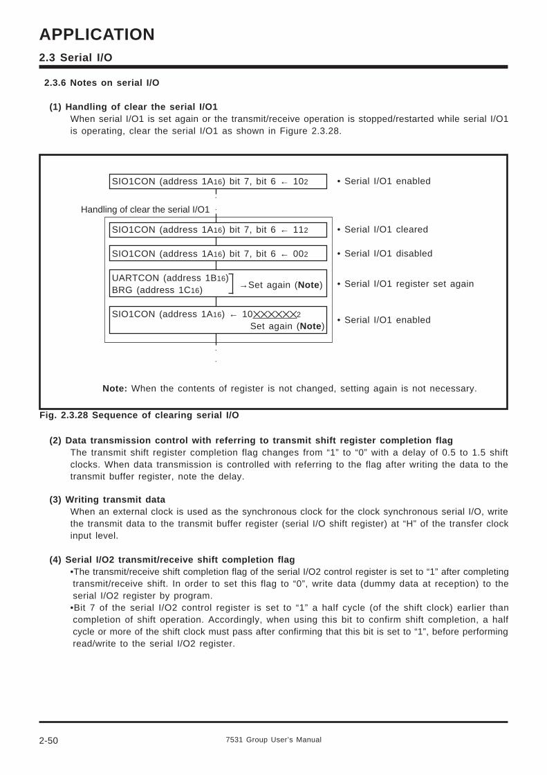
7531 Group User’s Manual2-50
APPLICATION2.3 Serial I/O
2.3.6 Notes on serial I/O
(1) Handling of clear the serial I/O1When serial I/O1 is set again or the transmit/receive operation is stopped/restarted while serial I/O1is operating, clear the serial I/O1 as shown in Figure 2.3.28.
Fig. 2.3.28 Sequence of clearing serial I/O
→Set again (Note )
• Serial I/O1 enabled
• Serial I/O1 cleared
• Serial I/O1 disabled
• Serial I/O1 register set again
• Serial I/O1 enabled
Handling of clear the serial I/O1
Note: When the contents of register is not changed, setting again is not necessary.
SIO1CON (address 1A16) bit 7, bit 6 ← 102
SIO1CON (address 1A16) bit 7, bit 6 ← 112
SIO1CON (address 1A16) bit 7, bit 6 ← 002
UARTCON (address 1B16)BRG (address 1C16)
SIO1CON (address 1A16) ← 102
Set again (Note )
(2) Data transmission control with referring to transmit shift register completion flagThe transmit shift register completion flag changes from “1” to “0” with a delay of 0.5 to 1.5 shiftclocks. When data transmission is controlled with referring to the flag after writing the data to thetransmit buffer register, note the delay.
(3) Writing transmit dataWhen an external clock is used as the synchronous clock for the clock synchronous serial I/O, writethe transmit data to the transmit buffer register (serial I/O shift register) at “H” of the transfer clockinput level.
(4) Serial I/O2 transmit/receive shift completion flag•The transmit/receive shift completion flag of the serial I/O2 control register is set to “1” after completingtransmit/receive shift. In order to set this flag to “0”, write data (dummy data at reception) to theserial I/O2 register by program.
•Bit 7 of the serial I/O2 control register is set to “1” a half cycle (of the shift clock) earlier thancompletion of shift operation. Accordingly, when using this bit to confirm shift completion, a halfcycle or more of the shift clock must pass after confirming that this bit is set to “1”, before performingread/write to the serial I/O2 register.
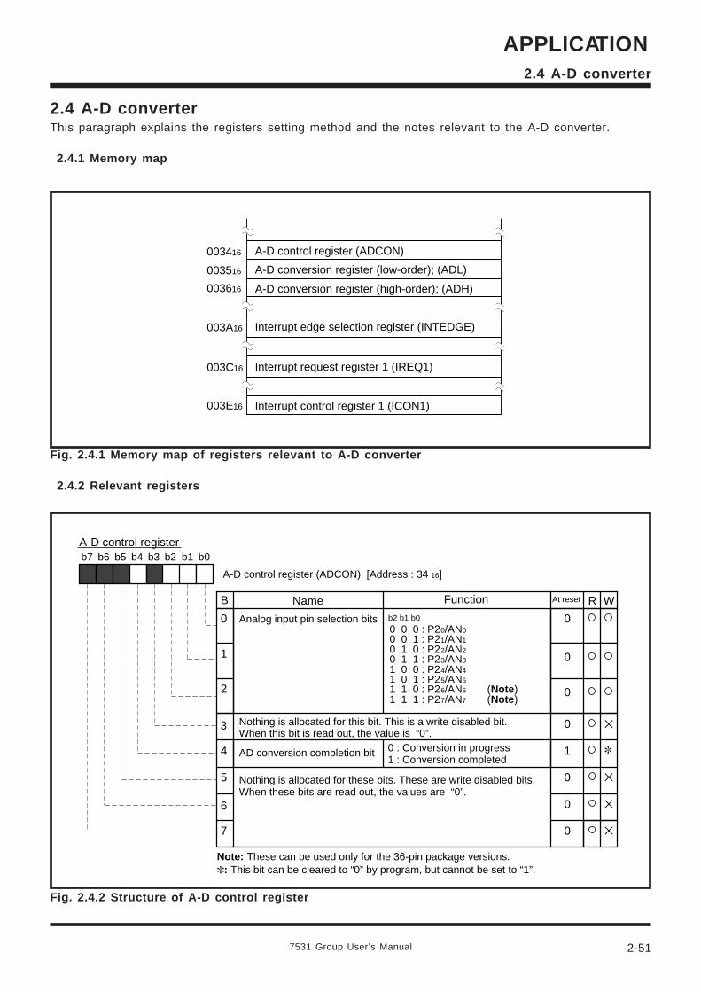
7531 Group User’s Manual
APPLICATION
2-51
2.4 A-D converter
2.4 A-D converterThis paragraph explains the registers setting method and the notes relevant to the A-D converter.
2.4.1 Memory map
Fig. 2.4.1 Memory map of registers relevant to A-D converter
2.4.2 Relevant registers
Fig. 2.4.2 Structure of A-D control register
003416
003516
003616
003C16
A-D control register (ADCON)
A-D conversion register (low-order); (ADL)
A-D conversion register (high-order); (ADH)
Interrupt request register 1 (IREQ1)
003E16 Interrupt control register 1 (ICON1)
003A16 Interrupt edge selection register (INTEDGE)
b7 b6 b5 b4 b3 b2 b1 b0
B Function At reset R W
0
1
2
3
4
5
6
7
Name
0
1
0
0
A-D control register (ADCON) [Address : 34 16]
Nothing is allocated for this bit. This is a write disabled bit.When this bit is read out, the value is “0”.
A-D control register
0
Note: These can be used only for the 36-pin package versions.
0 0 0 : P20/AN00 0 1 : P21/AN10 1 0 : P22/AN20 1 1 : P23/AN31 0 0 : P24/AN41 0 1 : P25/AN51 1 0 : P26/AN6 (Note)1 1 1 : P27/AN7 (Note)
Analog input pin selection bits b2 b1 b0
0
0
AD conversion completion bit 0 : Conversion in progress1 : Conversion completed
Nothing is allocated for these bits. These are write disabled bits.When these bits are read out, the values are “0”.
0
: This bit can be cleared to “0” by program, but cannot be set to “1”.
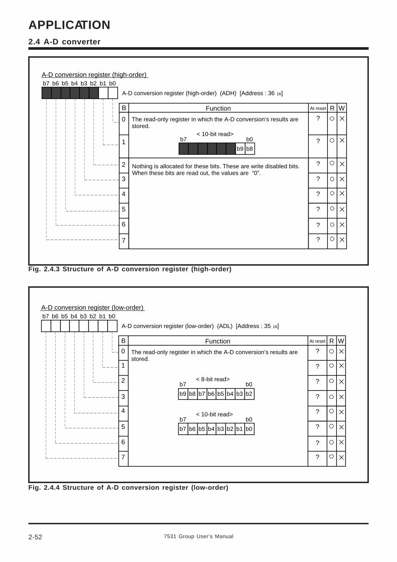
7531 Group User’s Manual2-52
APPLICATION2.4 A-D converter
Fig. 2.4.3 Structure of A-D conversion register (high-order)
Fig. 2.4.4 Structure of A-D conversion register (low-order)
A-D conversion register (high-order)b7 b6 b5 b4 b3 b2 b1 b0
B Function At reset R W
0
1
2
3
4
5
6
7
?
?
?
?
?
?
?
?
A-D conversion register (high-order) (ADH) [Address : 36 16]
The read-only register in which the A-D conversion’s results are stored.
< 10-bit read>b7
b9
b0
b8
Nothing is allocated for these bits. These are write disabled bits.When these bits are read out, the values are “0”.
A-D conversion register (low-order)b7 b6 b5 b4 b3 b2 b1 b0
B Function At reset R W
0
1
2
3
4
5
6
7
?
?
?
?
?
?
?
?
A-D conversion register (low-order) (ADL) [Address : 35 16]
The read-only register in which the A-D conversion’s results are stored.
< 8-bit read>b7
b8 b7 b6 b5 b4 b3
b0
b2b9
< 10-bit read>b7
b6 b5 b4 b3 b2 b1
b0
b0b7
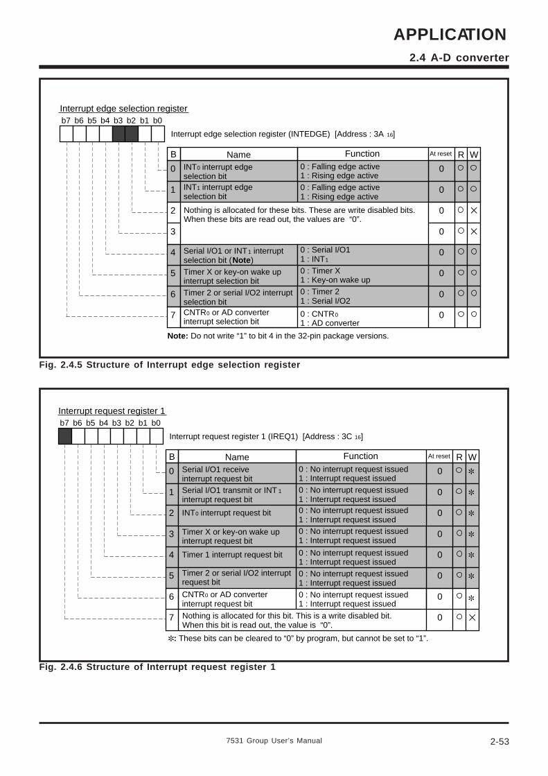
7531 Group User’s Manual
APPLICATION
2-53
2.4 A-D converter
Fig. 2.4.5 Structure of Interrupt edge selection register
Fig. 2.4.6 Structure of Interrupt request register 1
Interrupt request register 1b7 b6 b5 b4 b3 b2 b1 b0
B Function At reset R W
0
1
2
3
4
5
6
7
Name
0
0
0
0
0
0
0
0
Interrupt request register 1 (IREQ1) [Address : 3C 16]
Nothing is allocated for this bit. This is a write disabled bit.When this bit is read out, the value is “0”.
Serial I/O1 receive interrupt request bitSerial I/O1 transmit or INT 1 interrupt request bit
0 : No interrupt request issued1 : Interrupt request issued
Timer 2 or serial I/O2 interrupt request bit
CNTR0 or AD converter interrupt request bit
: These bits can be cleared to “0” by program, but cannot be set to “1”.
0 : No interrupt request issued1 : Interrupt request issued
INT0 interrupt request bit
Timer X or key-on wake up interrupt request bit
0 : No interrupt request issued1 : Interrupt request issued0 : No interrupt request issued1 : Interrupt request issued
Timer 1 interrupt request bit 0 : No interrupt request issued1 : Interrupt request issued0 : No interrupt request issued1 : Interrupt request issued0 : No interrupt request issued1 : Interrupt request issued
Interrupt edge selection registerb7 b6 b5 b4 b3 b2 b1 b0
B Function At reset R W
0
1
2
3
4
5
6
7
Name
0
0
0
0
0
0
0
0
Interrupt edge selection register (INTEDGE) [Address : 3A 16]
Nothing is allocated for these bits. These are write disabled bits.When these bits are read out, the values are “0”.
INT0 interrupt edge selection bitINT1 interrupt edge selection bit
0 : Falling edge active1 : Rising edge active0 : Falling edge active1 : Rising edge active
Serial I/O1 or INT1 interrupt selection bit (Note)Timer X or key-on wake up interrupt selection bitTimer 2 or serial I/O2 interrupt selection bitCNTR0 or AD converter interrupt selection bit
0 : Serial I/O11 : INT1
0 : Timer X1 : Key-on wake up0 : Timer 21 : Serial I/O2
0 : CNTR0
1 : AD converter
Note: Do not write “1” to bit 4 in the 32-pin package versions.
7531 Group User’s Manual2-54
APPLICATION2.4 A-D converter
Fig. 2.4.7 Structure of Interrupt control register 1
Interrupt control register 1b7 b6 b5 b4 b3 b2 b1 b0
B Function At reset R W
0
1
2
3
4
5
6
7
Name
0
0
0
0
0
0
0
0
Interrupt control register 1 (ICON1) [Address : 3E 16]
Nothing is allocated for this bit. Do not write “1” to this bit.When this bit is read out, the value is “0”.
Serial I/O1 receive interrupt enable bitSerial I/O1 transmit or INT 1 interrupt enable bit
0 : Interrupt disabled1 : Interrupt enabled
Timer 2 or serial I/O2 interrupt enable bit
CNTR0 or AD converter interrupt enable bit
INT0 interrupt enable bit
Timer X or key-on wake up interrupt enable bit
Timer 1 interrupt enable bit
0 : Interrupt disabled1 : Interrupt enabled0 : Interrupt disabled1 : Interrupt enabled0 : Interrupt disabled1 : Interrupt enabled0 : Interrupt disabled1 : Interrupt enabled0 : Interrupt disabled1 : Interrupt enabled0 : Interrupt disabled1 : Interrupt enabled
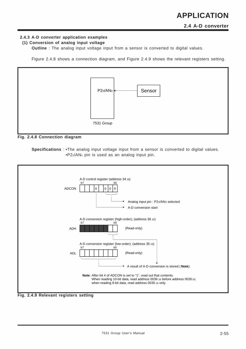
7531 Group User’s Manual
APPLICATION
2-55
2.4 A-D converter
2.4.3 A-D converter application examples(1) Conversion of analog input voltage
Outline : The analog input voltage input from a sensor is converted to digital values.
Figure 2.4.8 shows a connection diagram, and Figure 2.4.9 shows the relevant registers setting.
Fig. 2.4.8 Connection diagram
P20/AN0
7531 Group
Sensor
Specifications : •The analog input voltage input from a sensor is converted to digital values.•P20/AN0 pin is used as an analog input pin.
A-D control register (address 34 16)
ADCON 0
Analog input pin : P20/AN0 selected
A-D conversion start
000
b0b7
A-D conversion register (high-order); (address 36 16)
ADH
ADL
b0b7
b0b7
(Read-only)
A-D conversion register (low-order); (address 35 16)
(Read-only)
A result of A-D conversion is stored ( Note).
Note: After bit 4 of ADCON is set to “1”, read out that contents.When reading 10-bit data, read address 0036 16 before address 003516; when reading 8-bit data, read address 0035 16 only.
Fig. 2.4.9 Relevant registers setting
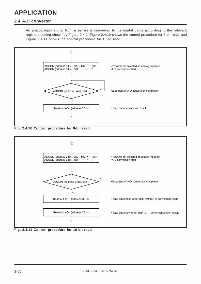
7531 Group User’s Manual2-56
APPLICATION2.4 A-D converter
An analog input signal from a sensor is converted to the digital value according to the relevantregisters setting shown by Figure 2.4.9. Figure 2.4.10 shows the control procedure for 8-bit read, andFigure 2.4.11 shows the control procedure for 10-bit read.
ADCON (address 3416), bit0 – bit2ADCON (address 3416), bit4
0002
0
Read out ADL (address 35 16)
ADCON (address 3416), bit4 ?
1
0
•P20/AN0 pin selected as analog input pin•A-D conversion start
•Judgment of A-D conversion completion
•Read out of conversion result
ADCON (address 3416), bit0 – bit2ADCON (address 3416), bit4
0002
0
Read out ADH (address 36 16)
ADCON (address 3416), bit4 ?
1
0
•P20/AN0 pin selected as analog input pin•A-D conversion start
•Judgment of A-D conversion completion
•Read out of high-order digit (b9, b8) of conversion result
Read out ADL (address 35 16) •Read out of low-order digit (b7 – b0) of conversion result
Fig. 2.4.10 Control procedure for 8-bit read
Fig. 2.4.11 Control procedure for 10-bit read
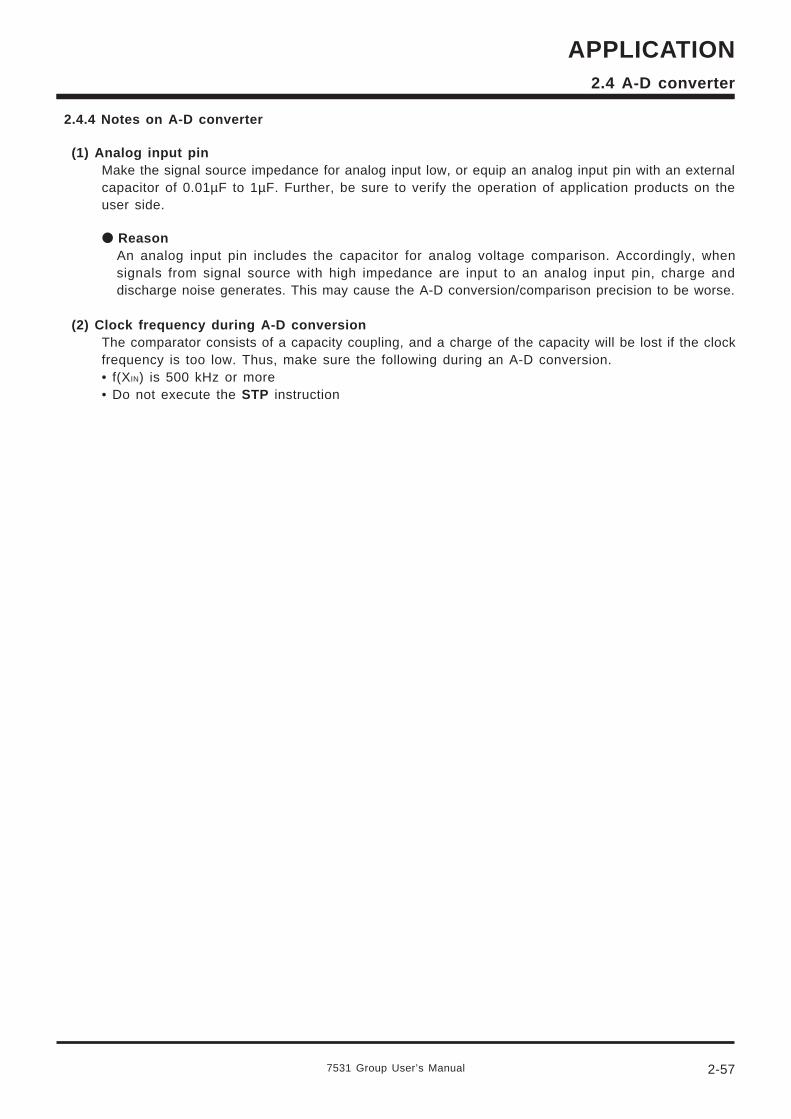
7531 Group User’s Manual
APPLICATION
2-57
2.4 A-D converter
2.4.4 Notes on A-D converter
(1) Analog input pinMake the signal source impedance for analog input low, or equip an analog input pin with an externalcapacitor of 0.01µF to 1µF. Further, be sure to verify the operation of application products on theuser side.
ReasonAn analog input pin includes the capacitor for analog voltage comparison. Accordingly, whensignals from signal source with high impedance are input to an analog input pin, charge anddischarge noise generates. This may cause the A-D conversion/comparison precision to be worse.
(2) Clock frequency during A-D conversionThe comparator consists of a capacity coupling, and a charge of the capacity will be lost if the clockfrequency is too low. Thus, make sure the following during an A-D conversion.• f(XIN) is 500 kHz or more• Do not execute the STP instruction
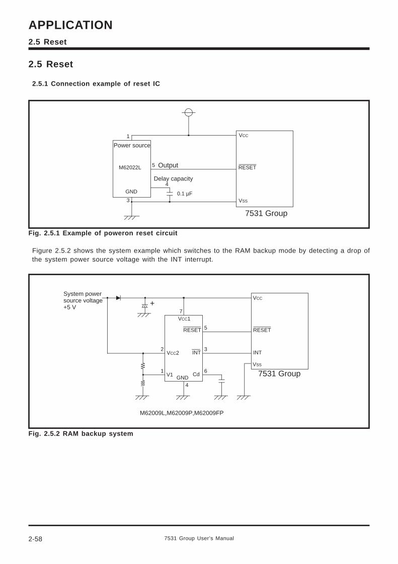
APPLICATION
7531 Group User’s Manual2-58
2.5 Reset
2.5 Reset
2.5.1 Connection example of reset IC
Fig. 2.5.1 Example of poweron reset circuit
Figure 2.5.2 shows the system example which switches to the RAM backup mode by detecting a drop ofthe system power source voltage with the INT interrupt.
VCC
RESET
VSS
M62022L
GND
1
3
4
5
0.1 µF
Power source
Output
Delay capacity
7531 Group
VCC
RESET
1
5RESET
INT
Cd
VCC1
VCC2
V1 GND
2
6
3
7
M62009L,M62009P,M62009FP
4
INT
VSS
System power source voltage+5 V +
7531 Group
Fig. 2.5.2 RAM backup system
7531 Group User’s Manual 2-59
APPLICATION2.5 Reset
2.5.2 Notes on RESET pin
Connecting capacitorIn case where the RESET signal rise time is long, connect a ceramic capacitor or others across theRESET pin and the VSS pin. Use a 1000 pF or more capacitor for high frequency use. Whenconnecting the capacitor, note the following :• Make the length of the wiring which is connected to a capacitor as short as possible.• Be sure to verify the operation of application products on the user side.
ReasonIf the several nanosecond or several ten nanosecond impulse noise enters the RESET pin, it maycause a microcomputer failure.

APPLICATION
7531 Group User’s Manual2-60
2.5 Reset
MEMO
CHAPTER 3APPENDIX
3.1 Electrical characteristics3.2 Typical characteristics3.3 Notes on use3.4 Countermeasures against noise3.5 List of registers3.6 Mask ROM confirmation form3.7 ROM programming confirmation form3.8 Mark specification form3.9 Package outline3.10 Machine instructions3.11 List of instruction code3.12 SFR memory map3.13 Pin configurations
3-2
APPENDIX
7531 Group User’s Manual
3.1 Electrical characteristics
3.1 Electrical characteristics
3.1.1 7531 Group (General purpose)Applied to: M37531M4-XXXFP/SP/GP, M37531M8-XXXFP/SP/GP, M37531E4FP/SP/GP, M37531E8FP/SP
(1) Absolute maximum ratings (General purpose)
Table 3.1.1 Absolute maximum ratings
–0.3 to 7.0
–0.3 to VCC + 0.3
–0.3 to VCC + 0.3
–0.3 to 13
–0.3 to VCC + 0.3
300 (Note 2)
–20 to 85
–40 to 125
Power source voltage
Input voltage P00–P07, P10–P14, P20–P27,P30–P37, VREF
Input voltage RESET, XIN
Input voltage CNVSS (Note 1)
Output voltage P00–P07, P10–P14, P20–P27,P30–P37, XOUT
Power dissipation
Operating temperature
Storage temperature
V
V
V
V
V
mW
°C
°C
VCC
VI
VI
VI
VO
Pd
Topr
Tstg
ConditionsSymbol Ratings UnitParameter
All voltages arebased on VSS.Output transistorsare cut off.
Ta = 25°C
Note 1: It is a rating only for the One Time PROM version. Connect to VSS for the mask ROM version.2: 200 mW for the 32P6B package product.
7531 Group User’s Manual 3-3
APPENDIX3.1 Electrical characteristics
(2) Recommended operating conditions (General purpose)
Table 3.1.2 Recommended operating conditions (1)(VCC = 2.2 to 5.5 V, Ta = –20 to 85 °C, unless otherwise noted)
5.5
5.5
5.5
5.5
5.5
5.5
5.5
5.5
5.5
VCC
VCC
4.0
2.4
2.2
4.0
2.4
2.2
4.0
2.4
2.2
2.0
0.8VCC
2.0
0.8VCC
0
0
0
0
Min. Typ. Max.Symbol Parameter Unit
Power source voltage (ceramic) f(XIN) = 8 MHz (High-, Middle-speed mode)
f(XIN) = 4 MHz (High-, Middle-speed mode)
f(XIN) = 2 MHz (High-, Middle-speed mode)
f(XIN) = 4 MHz (Double-speed mode)
f(XIN) = 2 MHz (Double-speed mode)
f(XIN) = 1 MHz (Double-speed mode)
f(XIN) = 4 MHz (High-, Middle-speed mode)
f(XIN) = 2 MHz (High-, Middle-speed mode)
f(XIN) = 1 MHz (High-, Middle-speed mode)
5.0
5.0
5.0
5.0
5.0
5.0
5.0
5.0
5.0
0
Limits
VCC V
V
V
V
V
V
V
V
V
V
V
V
Power source voltage
Analog reference voltage
“H” input voltage P00–P07, P10–P14, P20–P27,P30–P37
“H” input voltage (TTL input level selected) P10, P12, P13, P36, P37 (Note 1)
“H” input voltage RESET, XIN
“L” input voltage P00–P07, P10–P14, P20–P27,P30–P37
“L” input voltage (TTL input level selected) P10, P12, P13, P36, P37 (Note 1)
“L” input voltage RESET, CNVSS
“L” input voltage XIN
“H” total peak output current (Note 2) P00–P07, P10–P14, P20–P27,P30–P37
“L” total peak output current (Note 2) P00–P07, P10–P14, P20–P27,P37
“L” total peak output current (Note 2) P30–P36
“H” total average output current (Note 2) P00–P07, P10–P14, P20–P27,P30–P37
“L” total average output current (Note 2) P00–P07, P10–P14, P20–P27,P37
“L” total average output current (Note 2) P30–P36
Note 1: Vcc = 4.0 to 5.5V2: The total output current is the sum of all the currents flowing through all the applicable ports. The total average current is an average
value measured over 100 ms. The total peak current is the peak value of all the currents.
VCC
VCC
0.3VCC
0.8
0.2VCC
0.16VCC
–80
80
60
–40
40
30
VSS
VREF
VIH
VIH
VIH
VIL
VIL
VIL
VIL
∑IOH(peak)
∑IOL(peak)
∑IOL(peak)
∑IOH(avg)
∑IOL(avg)
∑IOL(avg)
Power source voltage (CR)
V
V
V
V
V
V
mA
mA
mA
mA
mA
mA
3-4
APPENDIX
7531 Group User’s Manual
3.1 Electrical characteristics
Table 3.1.3 Recommended operating conditions (2)(VCC = 2.2 to 5.5 V, Ta = –20 to 85 °C, unless otherwise noted)
“H” peak output current (Note 1) P00–P07, P10–P14, P20–P27,P30–P37
“L” peak output current (Note 1) P00–P07, P10–P14, P20–P27,P37
“L” peak output current (Note 1) P30–P36
“H” average output current (Note 2) P00–P07, P10–P14, P20–P27,P30–P37
“L” average output current (Note 2) P00–P07, P10–P14, P20–P27,P37
“L” average output current (Note 2) P30–P36
Oscillation frequency (Note 3) VCC = 4.0 to 5.5 Vat ceramic oscillation or external clock input Double-speed mode
Oscillation frequency (Note 3) VCC = 2.4 to 5.5 Vat ceramic oscillation or external clock input Double-speed mode
Oscillation frequency (Note 3) VCC = 2.2 to 5.5 Vat ceramic oscillation or external clock input Double-speed mode
Oscillation frequency (Note 3) VCC = 4.0 to 5.5 Vat ceramic oscillation or external clock input High-, Middle-speed mode
Oscillation frequency (Note 3) VCC = 2.4 to 5.5 Vat ceramic oscillation or external clock input High-, Middle-speed mode
Oscillation frequency (Note 3) VCC = 2.2 to 5.5 Vat ceramic oscillation or external clock input High-, Middle-speed mode
Oscillation frequency (Note 3) VCC = 4.0 to 5.5 Vat RC oscillation High-, Middle-speed mode
Oscillation frequency (Note 3) VCC = 2.4 to 5.5 Vat RC oscillation High-, Middle-speed mode
Oscillation frequency (Note 3) VCC = 2.2 to 5.5 Vat RC oscillation High-, Middle-speed mode
mA
mA
mA
mA
mA
mA
MHz
MHz
MHz
MHz
MHz
MHz
MHz
MHz
MHz
Symbol ParameterLimits
UnitMax.Typ.Min.
–10
10
30
–5
5
15
4
2
1
8
4
2
4
2
1
Notes 1: The peak output current is the peak current flowing in each port.2: The average output current IOL (avg), IOH (avg) in an average value measured over 100 ms.3: When the oscillation frequency has a duty cycle of 50 %.
IOH(peak)
IOL(peak)
IOL(peak)
IOH(avg)
IOL(avg)
IOL(avg)
f(XIN)
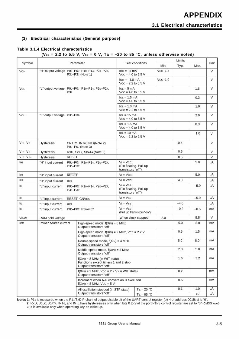
7531 Group User’s Manual 3-5
APPENDIX3.1 Electrical characteristics
(3) Electrical characteristics (General purpose)
Table 3.1.4 Electrical characteristics(VCC = 2.2 to 5.5 V, V SS = 0 V, Ta = –20 to 85 °C, unless otherwise noted)
Min. Typ. Max.Symbol Parameter
LimitsUnit
IOH = –5 mAVCC = 4.0 to 5.5 V
IOH = –1.0 mAVCC = 2.2 to 5.5 V
IOL = 5 mAVCC = 4.0 to 5.5 V
IOL = 1.5 mAVCC = 4.0 to 5.5 V
IOL = 1.0 mAVCC = 2.2 to 5.5 V
IOL = 15 mAVCC = 4.0 to 5.5 V
IOL = 1.5 mAVCC = 4.0 to 5.5 V
IOL = 10 mAVCC = 2.2 to 5.5 V
VI = VCC(Pin floating. Pull uptransistors “off”)
VI = VCC
VI = VCC
VI = VSS(Pin floating. Pull uptransistors “off”)
VI = VSS
VI = VSS
VI = VSS(Pull up transistors “on”)
Test conditions
VCC–1.5
VCC–1.0
“H” output voltage P00–P07, P10–P14, P20–P27,P30–P37 (Note 1)
“L” output voltage P00–P07, P10–P14, P20–P27,P37
“L” output voltage P30–P36
Hysteresis CNTR0, INT0, INT1(Note 2)P00–P07 (Note 3)
Hysteresis RXD, SCLK, SDATA (Note 2)
Hysteresis
“H” input current P00–P07, P10–P14, P20–P27,P30–P37
“H” input current RESET
“H” input current XIN
“L” input current P00–P07, P10–P14, P20–P27,P30–P37
“L” input current RESET, CNVSS
“L” input current XIN
“L” input current P00–P07, P30–P37
RAM hold voltage
1.5
0.3
1.0
2.0
0.3
V
V
V
V
V
V
V
VOH
VOL
VOL
0.4 VVT+–VT–
V
0.5
0.5
4.0
–4.0
–0.2
5.0
5.0
–5.0
–5.0
–0.5
5.5
V
µA
µA
µA
µA
µA
µA
mA
V
VT+–VT–
VT+–VT–
IIH
IIH
IIH
IIL
IIL
IIL
IIL
VRAM When clock stopped 2.0
RESET
1.0 V
ICC Power source current 5.0
Ta = 25 °C
Ta = 85 °C
0.5
5.0
2.0
0.1
1.6
0.2
0.5
8.0
1.5
8.0
5.0
1.0
10
mA
mA
mA
mA
mA
mA
mA
µA
µA
High-speed mode, f(XIN) = 8 MHzOutput transistors “off”
High-speed mode, f(XIN) = 2 MHz, VCC = 2.2 VOutput transistors “off”
Double-speed mode, f(XIN) = 4 MHzOutput transistors “off”
Middle-speed mode, f(XIN) = 8 MHzOutput transistors “off”
f(XIN) = 8 MHz (in WIT state)Functions except timers 1 and 2 stopOutput transistors “off”
f(XIN) = 2 MHz, VCC = 2.2 V (in WIT state)Output transistors “off”
Increment when A-D conversion is executedf(XIN) = 8 MHz, VCC = 5 V
All oscillation stopped (in STP state)Output transistors “off”
Notes 1: P11 is measured when the P11/TXD P-channel output disable bit of the UART control register (bit 4 of address 001B16) is “0”.2: RXD, SCLK, SDATA, INT0, and INT1 have hysteresises only when bits 0 to 2 of the port P1P3 control register are set to “0” (CMOS level).3: It is available only when operating key-on wake up.
3.2
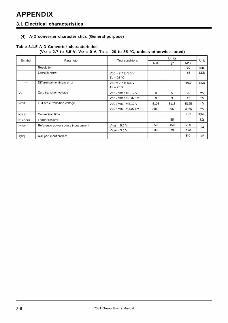
3-6
APPENDIX
7531 Group User’s Manual
3.1 Electrical characteristics
(4) A-D converter characteristics (General purpose)
Table 3.1.5 A-D Converter characteristics(VCC = 2.7 to 5.5 V, V SS = 0 V, Ta = –20 to 85 °C, unless otherwise noted)
VCC = VREF = 5.12 V
VCC = VREF = 3.072 V
Resolution
Linearity error
Differential nonlinear error
Zero transition voltage
Full scale transition voltage
Conversion time
Ladder resistor
Reference power source input current
A-D port input current
Min. Typ. Max.Symbol Parameter
LimitsUnitTest conditions
VCC = 2.7 to 5.5 VTa = 25 °C
VCC = 2.7 to 5.5 VTa = 25 °C
VCC = VREF = 5.12 V
VCC = VREF = 3.072 V
VREF = 5.0 V
0
0
5105
3060
50
30
5
3
5115
3069
20
15
5125
3075
122
200
55
150
mV
mV
mV
mV
tc(XIN)
kΩ
LSB
LSB
Bits
±0.9
±3
10—
—
—
VOT
VFST
tCONV
RLADDER
IVREF
II(AD) µA5.0
µAVREF = 3.0 V 12070
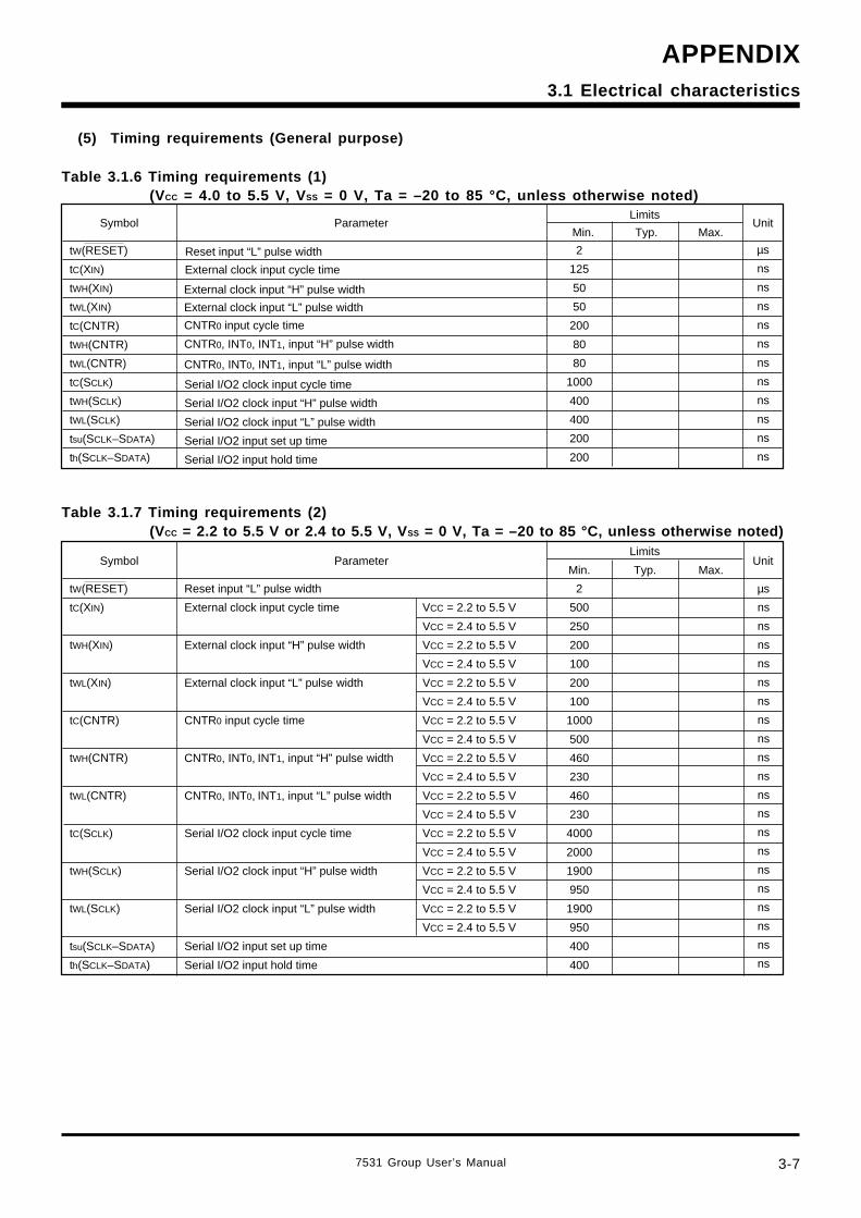
7531 Group User’s Manual 3-7
APPENDIX3.1 Electrical characteristics
(5) Timing requirements (General purpose)
Table 3.1.6 Timing requirements (1)(VCC = 4.0 to 5.5 V, V SS = 0 V, Ta = –20 to 85 °C, unless otherwise noted)
Min. Typ. Max.Symbol Parameter
LimitsUnit
tW(RESET)
tC(XIN)
tWH(XIN)
tWL(XIN)
tC(CNTR)
tWH(CNTR)
tWL(CNTR)
tC(SCLK)
tWH(SCLK)
tWL(SCLK)
tsu(SCLK–SDATA)
th(SCLK–SDATA)
Reset input “L” pulse width
External clock input cycle time
External clock input “H” pulse width
External clock input “L” pulse width
CNTR0 input cycle time
CNTR0, INT0, INT1, input “H” pulse width
CNTR0, INT0, INT1, input “L” pulse width
Serial I/O2 clock input cycle time
Serial I/O2 clock input “H” pulse width
Serial I/O2 clock input “L” pulse width
Serial I/O2 input set up time
Serial I/O2 input hold time
2
125
50
50
200
80
80
1000
400
400
200
200
µs
ns
ns
ns
ns
ns
ns
ns
ns
ns
ns
ns
Table 3.1.7 Timing requirements (2)(VCC = 2.2 to 5.5 V or 2.4 to 5.5 V, V SS = 0 V, Ta = –20 to 85 °C, unless otherwise noted)
Max.Symbol Parameter Unit
Min. Typ.
Limits
tW(RESET)
tC(XIN)
tWH(XIN)
tWL(XIN)
tC(CNTR)
tWH(CNTR)
tWL(CNTR)
tC(SCLK)
tWH(SCLK)
tWL(SCLK)
tsu(SCLK–SDATA)
th(SCLK–SDATA)
Reset input “L” pulse width
External clock input cycle time VCC = 2.2 to 5.5 V
VCC = 2.4 to 5.5 V
External clock input “H” pulse width VCC = 2.2 to 5.5 V
VCC = 2.4 to 5.5 V
External clock input “L” pulse width VCC = 2.2 to 5.5 V
VCC = 2.4 to 5.5 V
CNTR0 input cycle time VCC = 2.2 to 5.5 V
VCC = 2.4 to 5.5 V
CNTR0, INT0, INT1, input “H” pulse width VCC = 2.2 to 5.5 V
VCC = 2.4 to 5.5 V
CNTR0, INT0, INT1, input “L” pulse width VCC = 2.2 to 5.5 V
VCC = 2.4 to 5.5 V
Serial I/O2 clock input cycle time VCC = 2.2 to 5.5 V
VCC = 2.4 to 5.5 V
Serial I/O2 clock input “H” pulse width VCC = 2.2 to 5.5 V
VCC = 2.4 to 5.5 V
Serial I/O2 clock input “L” pulse width VCC = 2.2 to 5.5 V
VCC = 2.4 to 5.5 V
Serial I/O2 input set up time
Serial I/O2 input hold time
2
500
250
200
100
200
100
1000
500
460
230
460
230
4000
2000
1900
950
1900
950
400
400
µs
ns
ns
ns
ns
ns
ns
ns
ns
ns
ns
ns
ns
ns
ns
ns
ns
ns
ns
ns
ns
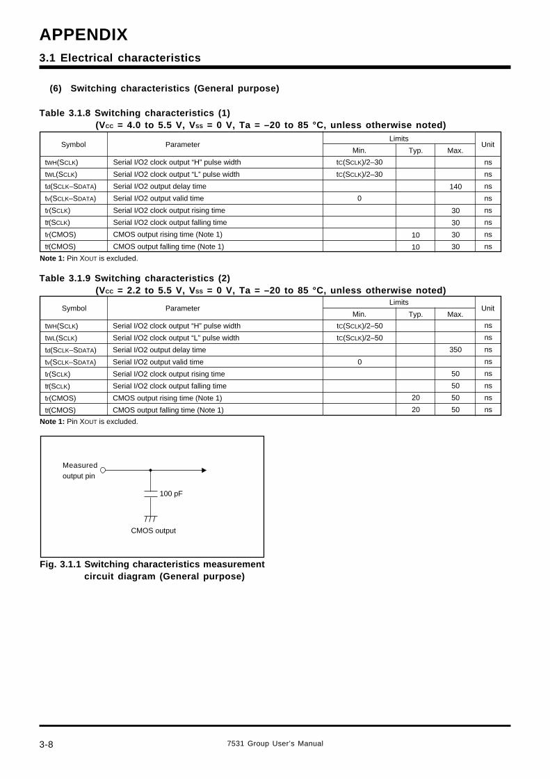
3-8
APPENDIX
7531 Group User’s Manual
3.1 Electrical characteristics
(6) Switching characteristics (General purpose)
Table 3.1.8 Switching characteristics (1)(VCC = 4.0 to 5.5 V, V SS = 0 V, Ta = –20 to 85 °C, unless otherwise noted)
tC(SCLK)/2–30
tC(SCLK)/2–30
0
Min. Typ. Max.Symbol Parameter
LimitsUnit
tWH(SCLK)
tWL(SCLK)
td(SCLK–SDATA)
tv(SCLK–SDATA)
tr(SCLK)
tf(SCLK)
tr(CMOS)
tf(CMOS)
Serial I/O2 clock output “H” pulse width
Serial I/O2 clock output “L” pulse width
Serial I/O2 output delay time
Serial I/O2 output valid time
Serial I/O2 clock output rising time
Serial I/O2 clock output falling time
CMOS output rising time (Note 1)
CMOS output falling time (Note 1)
140
30
30
30
30
ns
ns
ns
ns
ns
ns
ns
ns
10
10
Note 1: Pin XOUT is excluded.
Table 3.1.9 Switching characteristics (2)(VCC = 2.2 to 5.5 V, V SS = 0 V, Ta = –20 to 85 °C, unless otherwise noted)
Serial I/O2 clock output “H” pulse width
Serial I/O2 clock output “L” pulse width
Serial I/O2 output delay time
Serial I/O2 output valid time
Serial I/O2 clock output rising time
Serial I/O2 clock output falling time
CMOS output rising time (Note 1)
CMOS output falling time (Note 1)
Min. Typ. Max.Symbol Parameter
LimitsUnit
tWH(SCLK)
tWL(SCLK)
td(SCLK–SDATA)
tv(SCLK–SDATA)
tr(SCLK)
tf(SCLK)
tr(CMOS)
tf(CMOS)
tC(SCLK)/2–50
tC(SCLK)/2–50
0
20
20
350
50
50
50
50
ns
ns
ns
ns
ns
ns
ns
ns
Note 1: Pin XOUT is excluded.
Fig. 3.1.1 Switching characteristics measurementcircuit diagram (General purpose)
/ / /
Measuredoutput pin
CMOS output
100 pF
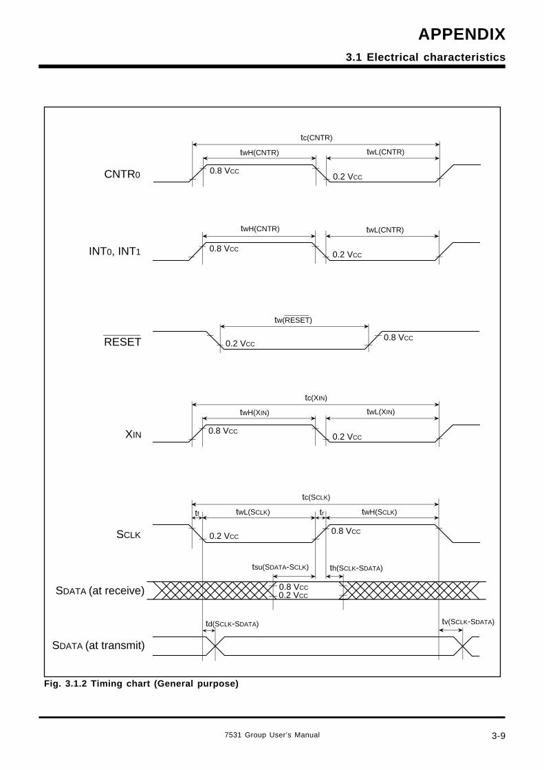
7531 Group User’s Manual 3-9
APPENDIX3.1 Electrical characteristics
Fig. 3.1.2 Timing chart (General purpose)
0.2 VCC
twL(CNTR)
0.8 VCC
twH(CNTR)
0.2 VCC
0.2 VCC0.8 VCC
0.8 VCC
0.2 VCC
twL(XIN)
0.8 VCC
twH(XIN)
tc(XIN)
XIN
0.2 VCC0.8 VCC
tw(RESET)
RESET
tf tr
0.2 VCC
twL(CNTR)
0.8 VCC
twH(CNTR)
tc(CNTR)
td(SCLK-SDATA) tv(SCLK-SDATA)
tc(SCLK)
twL(SCLK) twH(SCLK)
th(SCLK-SDATA)tsu(SDATA-SCLK)
SDATA (at transmit)
SDATA (at receive)
SCLK
INT0, INT1
CNTR0
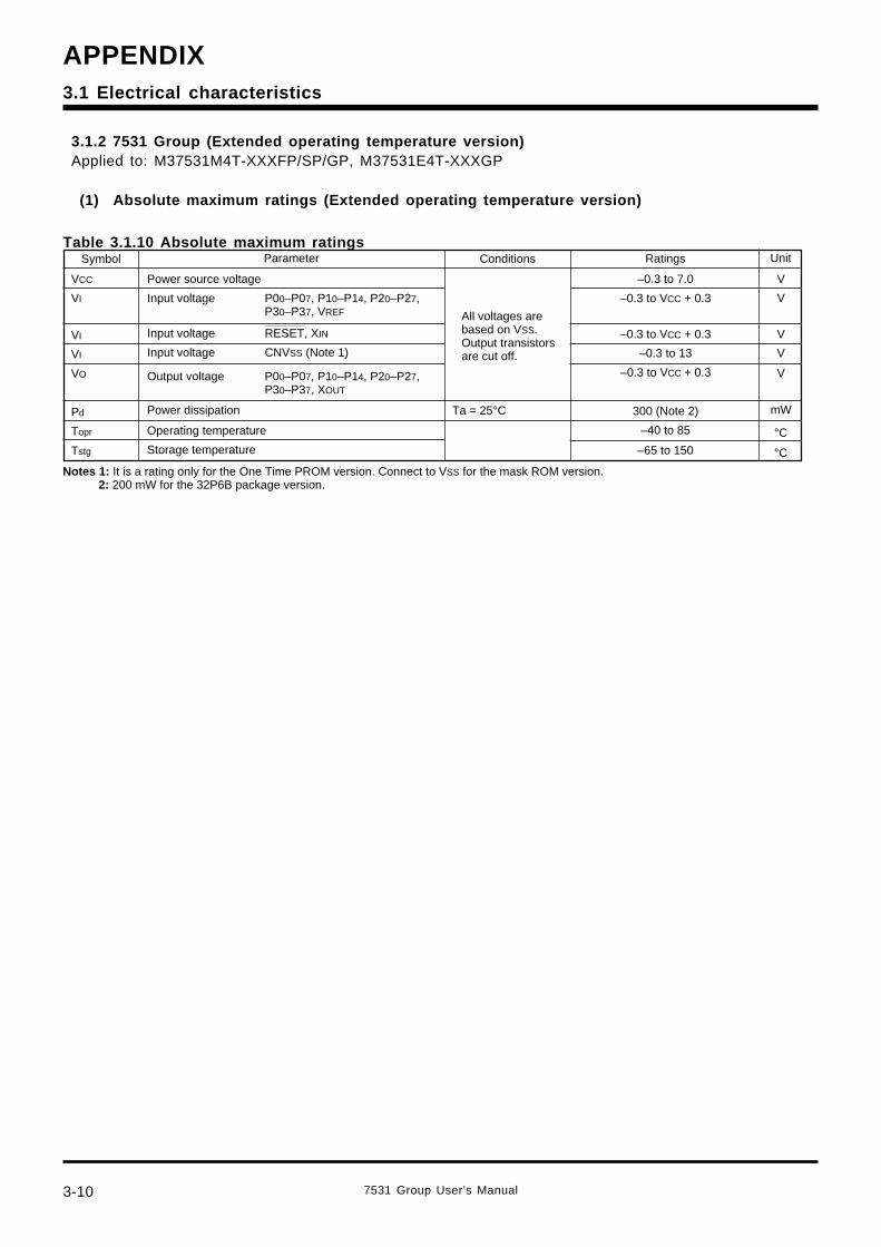
3-10
APPENDIX
7531 Group User’s Manual
3.1 Electrical characteristics
3.1.2 7531 Group (Extended operating temperature version)Applied to: M37531M4T-XXXFP/SP/GP, M37531E4T-XXXGP
(1) Absolute maximum ratings (Extended operating temperature version)
Table 3.1.10 Absolute maximum ratings
–0.3 to 7.0
–0.3 to VCC + 0.3
–0.3 to VCC + 0.3
–0.3 to 13
–0.3 to VCC + 0.3
300 (Note 2)
–40 to 85
–65 to 150
Power source voltage
Input voltage P00–P07, P10–P14, P20–P27,P30–P37, VREF
Input voltage RESET, XIN
Input voltage CNVSS (Note 1)
Output voltage P00–P07, P10–P14, P20–P27,P30–P37, XOUT
Power dissipation
Operating temperature
Storage temperature
V
V
V
V
V
mW
°C
°C
VCC
VI
VI
VI
VO
Pd
Topr
Tstg
ConditionsSymbol Ratings UnitParameter
All voltages arebased on VSS.Output transistorsare cut off.
Ta = 25°C
Notes 1: It is a rating only for the One Time PROM version. Connect to VSS for the mask ROM version.2: 200 mW for the 32P6B package version.
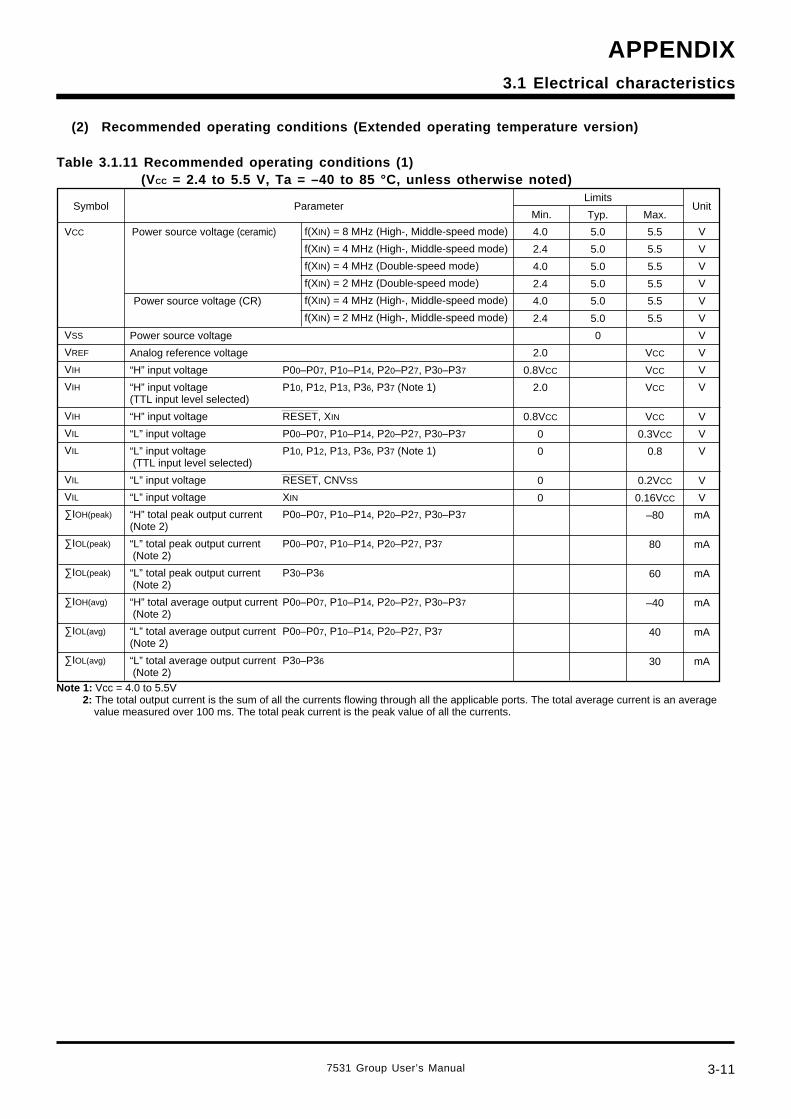
7531 Group User’s Manual 3-11
APPENDIX3.1 Electrical characteristics
(2) Recommended operating conditions (Extended operating temperature version)
Table 3.1.11 Recommended operating conditions (1)(VCC = 2.4 to 5.5 V, Ta = –40 to 85 °C, unless otherwise noted)
5.5
5.5
5.5
5.5
5.5
5.5
VCC
VCC
VCC
VCC
0.3VCC
0.8
0.2VCC
0.16VCC
–80
80
60
–40
40
30
4.0
2.4
4.0
2.4
4.0
2.4
2.0
0.8VCC
2.0
0.8VCC
0
0
0
0
Min. Typ. Max.Symbol Parameter Unit
Power source voltage (ceramic) f(XIN) = 8 MHz (High-, Middle-speed mode)
f(XIN) = 4 MHz (High-, Middle-speed mode)
f(XIN) = 4 MHz (Double-speed mode)
f(XIN) = 2 MHz (Double-speed mode)
f(XIN) = 4 MHz (High-, Middle-speed mode)
f(XIN) = 2 MHz (High-, Middle-speed mode)
5.0
5.0
5.0
5.0
5.0
5.0
0
Limits
VCC
VSS
VREF
VIH
VIH
VIH
VIL
VIL
VIL
VIL
∑IOH(peak)
∑IOL(peak)
∑IOL(peak)
∑IOH(avg)
∑IOL(avg)
∑IOL(avg)
V
V
V
V
V
V
V
V
V
V
V
V
V
V
V
mA
mA
mA
mA
mA
mA
Power source voltage
Analog reference voltage
“H” input voltage P00–P07, P10–P14, P20–P27, P30–P37
“H” input voltage P10, P12, P13, P36, P37 (Note 1)(TTL input level selected)
“H” input voltage RESET, XIN
“L” input voltage P00–P07, P10–P14, P20–P27, P30–P37
“L” input voltage P10, P12, P13, P36, P37 (Note 1) (TTL input level selected)
“L” input voltage RESET, CNVSS
“L” input voltage XIN
“H” total peak output current P00–P07, P10–P14, P20–P27, P30–P37(Note 2)
“L” total peak output current P00–P07, P10–P14, P20–P27, P37 (Note 2)
“L” total peak output current P30–P36 (Note 2)
“H” total average output current P00–P07, P10–P14, P20–P27, P30–P37 (Note 2)
“L” total average output current P00–P07, P10–P14, P20–P27, P37(Note 2)
“L” total average output current P30–P36 (Note 2)
Note 1: Vcc = 4.0 to 5.5V2: The total output current is the sum of all the currents flowing through all the applicable ports. The total average current is an average
value measured over 100 ms. The total peak current is the peak value of all the currents.
Power source voltage (CR)
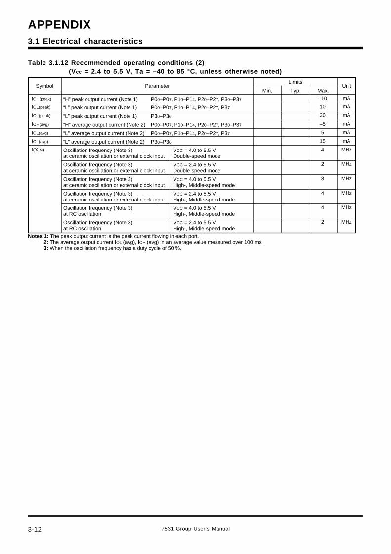
3-12
APPENDIX
7531 Group User’s Manual
3.1 Electrical characteristics
Table 3.1.12 Recommended operating conditions (2)(VCC = 2.4 to 5.5 V, Ta = –40 to 85 °C, unless otherwise noted)
“H” peak output current (Note 1) P00–P07, P10–P14, P20–P27, P30–P37
“L” peak output current (Note 1) P00–P07, P10–P14, P20–P27, P37
“L” peak output current (Note 1) P30–P36
“H” average output current (Note 2) P00–P07, P10–P14, P20–P27, P30–P37
“L” average output current (Note 2) P00–P07, P10–P14, P20–P27, P37
“L” average output current (Note 2) P30–P36
Oscillation frequency (Note 3) VCC = 4.0 to 5.5 Vat ceramic oscillation or external clock input Double-speed mode
Oscillation frequency (Note 3) VCC = 2.4 to 5.5 Vat ceramic oscillation or external clock input Double-speed mode
Oscillation frequency (Note 3) VCC = 4.0 to 5.5 Vat ceramic oscillation or external clock input High-, Middle-speed mode
Oscillation frequency (Note 3) VCC = 2.4 to 5.5 Vat ceramic oscillation or external clock input High-, Middle-speed mode
Oscillation frequency (Note 3) VCC = 4.0 to 5.5 Vat RC oscillation High-, Middle-speed mode
Oscillation frequency (Note 3) VCC = 2.4 to 5.5 Vat RC oscillation High-, Middle-speed mode
mA
mA
mA
mA
mA
mA
MHz
MHz
MHz
MHz
MHz
MHz
Symbol ParameterLimits
UnitMax.Typ.Min.
–10
10
30
–5
5
15
4
2
8
4
4
2
Notes 1: The peak output current is the peak current flowing in each port.2: The average output current IOL (avg), IOH (avg) in an average value measured over 100 ms.3: When the oscillation frequency has a duty cycle of 50 %.
IOH(peak)
IOL(peak)
IOL(peak)
IOH(avg)
IOL(avg)
IOL(avg)
f(XIN)
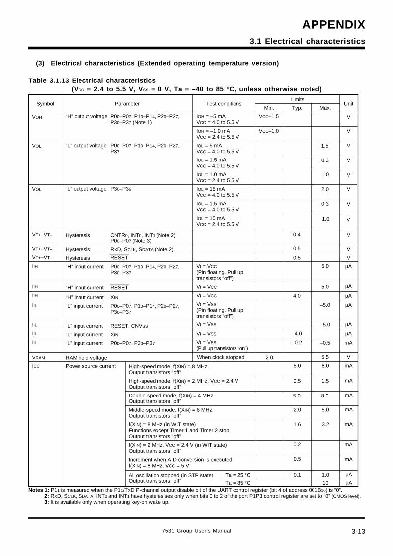
7531 Group User’s Manual 3-13
APPENDIX3.1 Electrical characteristics
(3) Electrical characteristics (Extended operating temperature version)
Table 3.1.13 Electrical characteristics(VCC = 2.4 to 5.5 V, V SS = 0 V, Ta = –40 to 85 °C, unless otherwise noted)
Min. Typ. Max.Symbol Parameter
LimitsUnit
IOH = –5 mAVCC = 4.0 to 5.5 V
IOH = –1.0 mAVCC = 2.4 to 5.5 V
IOL = 5 mAVCC = 4.0 to 5.5 V
IOL = 1.5 mAVCC = 4.0 to 5.5 V
IOL = 1.0 mAVCC = 2.4 to 5.5 V
IOL = 15 mAVCC = 4.0 to 5.5 V
IOL = 1.5 mAVCC = 4.0 to 5.5 V
IOL = 10 mAVCC = 2.4 to 5.5 V
VI = VCC(Pin floating. Pull uptransistors “off”)
VI = VCC
VI = VCC
VI = VSS(Pin floating. Pull uptransistors “off”)
VI = VSS
VI = VSS
VI = VSS(Pull up transistors “on”)
Test conditions
VCC–1.5
VCC–1.0
“H” output voltage P00–P07, P10–P14, P20–P27,P30–P37 (Note 1)
“L” output voltage P00–P07, P10–P14, P20–P27,P37
“L” output voltage P30–P36
Hysteresis CNTR0, INT0, INT1 (Note 2)P00–P07 (Note 3)
Hysteresis RXD, SCLK, SDATA (Note 2)
Hysteresis
“H” input current P00–P07, P10–P14, P20–P27,P30–P37
“H” input current RESET
“H” input current XIN
“L” input current P00–P07, P10–P14, P20–P27,P30–P37
“L” input current RESET, CNVSS
“L” input current XIN
“L” input current P00–P07, P30–P37
RAM hold voltage
1.5
0.3
1.0
2.0
0.3
V
V
V
V
V
V
V
VOH
VOL
VOL
0.4 VVT+–VT–
V
0.5
0.5
4.0
–4.0
–0.2
5.0
5.0
–5.0
–5.0
–0.5
5.5
V
µA
µA
µA
µA
µA
µA
mA
V
VT+–VT–
VT+–VT–
IIH
IIH
IIH
IIL
IIL
IIL
IIL
VRAM When clock stopped 2.0
RESET
1.0 V
ICC Power source current 5.0
Ta = 25 °C
Ta = 85 °C
0.5
5.0
2.0
0.1
1.6
0.2
0.5
8.0
1.5
8.0
5.0
1.0
10
mA
mA
mA
mA
mA
mA
mA
µA
µA
High-speed mode, f(XIN) = 8 MHzOutput transistors “off”
High-speed mode, f(XIN) = 2 MHz, VCC = 2.4 VOutput transistors “off”
Double-speed mode, f(XIN) = 4 MHzOutput transistors “off”
Middle-speed mode, f(XIN) = 8 MHz,Output transistors “off”
f(XIN) = 8 MHz (in WIT state)Functions except Timer 1 and Timer 2 stopOutput transistors “off”
f(XIN) = 2 MHz, VCC = 2.4 V (in WIT state)Output transistors “off”
Increment when A-D conversion is executedf(XIN) = 8 MHz, VCC = 5 V
All oscillation stopped (in STP state)Output transistors “off”
Notes 1: P11 is measured when the P11/TXD P-channel output disable bit of the UART control register (bit 4 of address 001B16) is “0”.2: RXD, SCLK, SDATA, INT0 and INT1 have hysteresises only when bits 0 to 2 of the port P1P3 control register are set to “0” (CMOS level).3: It is available only when operating key-on wake up.
3.2

3-14
APPENDIX
7531 Group User’s Manual
3.1 Electrical characteristics
(4) A-D converter characteristics (Extended operating temperature version)
Table 3.1.14 A-D Converter characteristics(VCC = 2.7 to 5.5 V, V SS = 0 V, Ta = –40 to 85 °C, unless otherwise noted)
VCC = VREF = 5.12 V
VCC = VREF = 3.072 V
Resolution
Linearity error
Differential nonlinear error
Zero transition voltage
Full scale transition voltage
Conversion time
Ladder resistor
Reference power source input current
A-D port input current
Min. Typ. Max.Symbol Parameter
LimitsUnitTest conditions
VCC = 2.7 to 5.5 VTa = 25 °C
VCC = 2.7 to 5.5 VTa = 25 °C
VCC = VREF = 5.12 V
VCC = VREF = 3.072 V
VREF = 5.0 V
0
0
5105
3060
50
30
5
3
5115
3069
20
15
5125
3075
122
200
55
150
mV
mV
mV
mV
tc(XIN)
kΩ
LSB
LSB
Bits
±0.9
±3
10—
—
—
VOT
VFST
tCONV
RLADDER
IVREF
II(AD) µA5.0
µAVREF = 3.0 V 12070
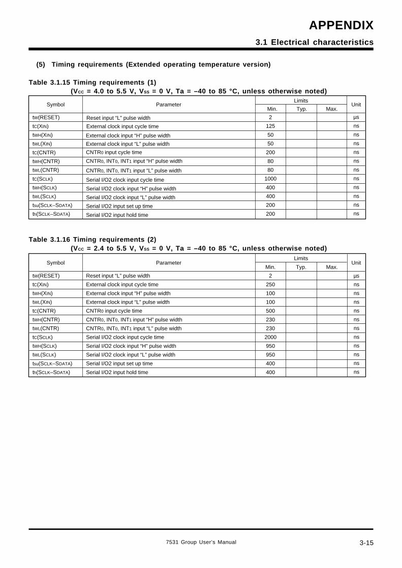
7531 Group User’s Manual 3-15
APPENDIX3.1 Electrical characteristics
(5) Timing requirements (Extended operating temperature version)
Table 3.1.15 Timing requirements (1)(VCC = 4.0 to 5.5 V, V SS = 0 V, Ta = –40 to 85 °C, unless otherwise noted)
Min. Typ. Max.Symbol Parameter
LimitsUnit
tW(RESET)
tC(XIN)
tWH(XIN)
tWL(XIN)
tC(CNTR)
tWH(CNTR)
tWL(CNTR)
tC(SCLK)
tWH(SCLK)
tWL(SCLK)
tsu(SCLK–SDATA)
th(SCLK–SDATA)
Reset input “L” pulse width
External clock input cycle time
External clock input “H” pulse width
External clock input “L” pulse width
CNTR0 input cycle time
CNTR0, INT0, INT1 input “H” pulse width
CNTR0, INT0, INT1 input “L” pulse width
Serial I/O2 clock input cycle time
Serial I/O2 clock input “H” pulse width
Serial I/O2 clock input “L” pulse width
Serial I/O2 input set up time
Serial I/O2 input hold time
2
125
50
50
200
80
80
1000
400
400
200
200
µs
ns
ns
ns
ns
ns
ns
ns
ns
ns
ns
ns
Table 3.1.16 Timing requirements (2)(VCC = 2.4 to 5.5 V, V SS = 0 V, Ta = –40 to 85 °C, unless otherwise noted)
Max.Symbol Parameter Unit
Min. Typ.
Limits
tW(RESET)
tC(XIN)
tWH(XIN)
tWL(XIN)
tC(CNTR)
tWH(CNTR)
tWL(CNTR)
tC(SCLK)
tWH(SCLK)
tWL(SCLK)
tsu(SCLK–SDATA)
th(SCLK–SDATA)
Reset input “L” pulse width
External clock input cycle time
External clock input “H” pulse width
External clock input “L” pulse width
CNTR0 input cycle time
CNTR0, INT0, INT1 input “H” pulse width
CNTR0, INT0, INT1 input “L” pulse width
Serial I/O2 clock input cycle time
Serial I/O2 clock input “H” pulse width
Serial I/O2 clock input “L” pulse width
Serial I/O2 input set up time
Serial I/O2 input hold time
2
250
100
100
500
230
230
2000
950
950
400
400
µs
ns
ns
ns
ns
ns
ns
ns
ns
ns
ns
ns
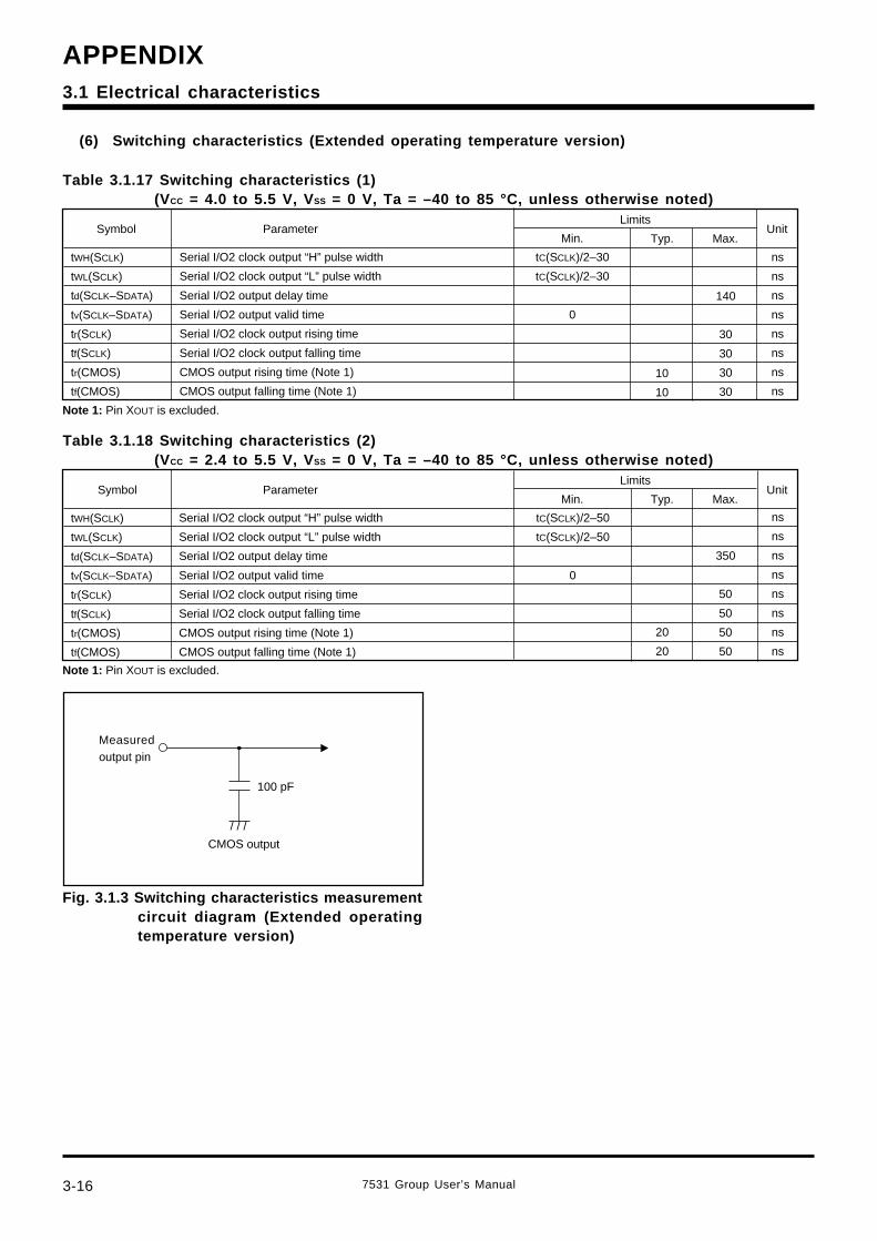
3-16
APPENDIX
7531 Group User’s Manual
3.1 Electrical characteristics
(6) Switching characteristics (Extended operating temperature version)
Table 3.1.17 Switching characteristics (1)(VCC = 4.0 to 5.5 V, V SS = 0 V, Ta = –40 to 85 °C, unless otherwise noted)
tC(SCLK)/2–30
tC(SCLK)/2–30
0
Min. Typ. Max.Symbol Parameter
LimitsUnit
tWH(SCLK)
tWL(SCLK)
td(SCLK–SDATA)
tv(SCLK–SDATA)
tr(SCLK)
tf(SCLK)
tr(CMOS)
tf(CMOS)
Serial I/O2 clock output “H” pulse width
Serial I/O2 clock output “L” pulse width
Serial I/O2 output delay time
Serial I/O2 output valid time
Serial I/O2 clock output rising time
Serial I/O2 clock output falling time
CMOS output rising time (Note 1)
CMOS output falling time (Note 1)
140
30
30
30
30
ns
ns
ns
ns
ns
ns
ns
ns
10
10
Note 1: Pin XOUT is excluded.
Table 3.1.18 Switching characteristics (2)(VCC = 2.4 to 5.5 V, V SS = 0 V, Ta = –40 to 85 °C, unless otherwise noted)
Serial I/O2 clock output “H” pulse width
Serial I/O2 clock output “L” pulse width
Serial I/O2 output delay time
Serial I/O2 output valid time
Serial I/O2 clock output rising time
Serial I/O2 clock output falling time
CMOS output rising time (Note 1)
CMOS output falling time (Note 1)
Min. Typ. Max.Symbol Parameter
LimitsUnit
tWH(SCLK)
tWL(SCLK)
td(SCLK–SDATA)
tv(SCLK–SDATA)
tr(SCLK)
tf(SCLK)
tr(CMOS)
tf(CMOS)
tC(SCLK)/2–50
tC(SCLK)/2–50
0
20
20
350
50
50
50
50
ns
ns
ns
ns
ns
ns
ns
ns
Note 1: Pin XOUT is excluded.
Fig. 3.1.3 Switching characteristics measurementcircuit diagram (Extended operatingtemperature version)
/ / /
Measuredoutput pin
CMOS output
100 pF
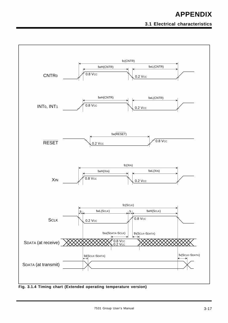
7531 Group User’s Manual 3-17
APPENDIX3.1 Electrical characteristics
Fig. 3.1.4 Timing chart (Extended operating temperature version)
0.2 VCC
twL(CNTR)
0.8 VCC
twH(CNTR)
0.2 VCC
0.2 VCC0.8 VCC
0.8 VCC
0.2 VCC
twL(XIN)
0.8 VCC
twH(XIN)
tc(XIN)
XIN
0.2 VCC0.8 VCC
tw(RESET)
RESET
tf tr
0.2 VCC
twL(CNTR)
0.8 VCC
twH(CNTR)
tc(CNTR)
td(SCLK-SDATA) tv(SCLK-SDATA)
tc(SCLK)
twL(SCLK) twH(SCLK)
th(SCLK-SDATA)tsu(SDATA-SCLK)
SDATA (at transmit)
SDATA (at receive)
SCLK
INT0, INT1
CNTR0
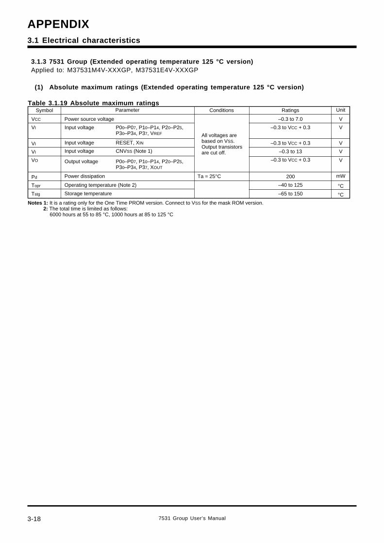
3-18
APPENDIX
7531 Group User’s Manual
3.1 Electrical characteristics
3.1.3 7531 Group (Extended operating temperature 125 °C version)Applied to: M37531M4V-XXXGP, M37531E4V-XXXGP
(1) Absolute maximum ratings (Extended operating temperature 125 °C version)
Table 3.1.19 Absolute maximum ratings
–0.3 to 7.0
–0.3 to VCC + 0.3
–0.3 to VCC + 0.3
–0.3 to 13
–0.3 to VCC + 0.3
200
–40 to 125
–65 to 150
Power source voltage
Input voltage P00–P07, P10–P14, P20–P25,P30–P34, P37, VREF
Input voltage RESET, XIN
Input voltage CNVSS (Note 1)
Output voltage P00–P07, P10–P14, P20–P25,P30–P34, P37, XOUT
Power dissipation
Operating temperature (Note 2)
Storage temperature
V
V
V
V
V
mW
°C
°C
VCC
VI
VI
VI
VO
Pd
Topr
Tstg
ConditionsSymbol Ratings UnitParameter
All voltages arebased on VSS.Output transistorsare cut off.
Ta = 25°C
Notes 1: It is a rating only for the One Time PROM version. Connect to VSS for the mask ROM version.2: The total time is limited as follows:
6000 hours at 55 to 85 °C, 1000 hours at 85 to 125 °C
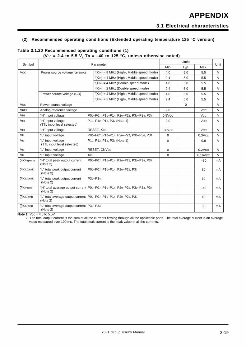
7531 Group User’s Manual 3-19
APPENDIX3.1 Electrical characteristics
(2) Recommended operating conditions (Extended operating temperature 125 °C version)
Table 3.1.20 Recommended operating conditions (1)(VCC = 2.4 to 5.5 V, Ta = –40 to 125 °C, unless otherwise noted)
5.5
5.5
5.5
5.5
5.5
5.5
VCC
VCC
VCC
VCC
0.3VCC
0.8
0.2VCC
0.16VCC
–80
80
60
–40
40
30
4.0
2.4
4.0
2.4
4.0
2.4
2.0
0.8VCC
2.0
0.8VCC
0
0
0
0
Min. Typ. Max.Symbol Parameter Unit
Power source voltage (ceramic) f(XIN) = 8 MHz (High-, Middle-speed mode)
f(XIN) = 4 MHz (High-, Middle-speed mode)
f(XIN) = 4 MHz (Double-speed mode)
f(XIN) = 2 MHz (Double-speed mode)
f(XIN) = 4 MHz (High-, Middle-speed mode)
f(XIN) = 2 MHz (High-, Middle-speed mode)
5.0
5.0
5.0
5.0
5.0
5.0
0
Limits
VCC
VSS
VREF
VIH
VIH
VIH
VIL
VIL
VIL
VIL
∑IOH(peak)
∑IOL(peak)
∑IOL(peak)
∑IOH(avg)
∑IOL(avg)
∑IOL(avg)
V
V
V
V
V
V
V
V
V
V
V
V
V
V
V
mA
mA
mA
mA
mA
mA
Power source voltage
Analog reference voltage
“H” input voltage P00–P07, P10–P14, P20–P25, P30–P34, P37
“H” input voltage P10, P12, P13, P37 (Note 1)(TTL input level selected)
“H” input voltage RESET, XIN
“L” input voltage P00–P07, P10–P14, P20–P25, P30–P34, P37
“L” input voltage P10, P12, P13, P37 (Note 1) (TTL input level selected)
“L” input voltage RESET, CNVSS
“L” input voltage XIN
“H” total peak output current P00–P07, P10–P14, P20–P25, P30–P34, P37(Note 2)
“L” total peak output current P00–P07, P10–P14, P20–P25, P37 (Note 2)
“L” total peak output current P30–P34 (Note 2)
“H” total average output current P00–P07, P10–P14, P20–P25, P30–P34, P37 (Note 2)
“L” total average output current P00–P07, P10–P14, P20–P25, P37(Note 2)
“L” total average output current P30–P34 (Note 2)
Note 1: Vcc = 4.0 to 5.5V2: The total output current is the sum of all the currents flowing through all the applicable ports. The total average current is an average
value measured over 100 ms. The total peak current is the peak value of all the currents.
Power source voltage (CR)

3-20
APPENDIX
7531 Group User’s Manual
3.1 Electrical characteristics
Table 3.1.21 Recommended operating conditions (2)(VCC = 2.4 to 5.5 V, Ta = –40 to 125 °C, unless otherwise noted)
“H” peak output current (Note 1) P00–P07, P10–P14, P20–P25, P30–P34, P37
“L” peak output current (Note 1) P00–P07, P10–P14, P20–P25, P37
“L” peak output current (Note 1) P30–P34
“H” average output current (Note 2) P00–P07, P10–P14, P20–P25, P30–P34, P37
“L” average output current (Note 2) P00–P07, P10–P14, P20–P25, P37
“L” average output current (Note 2) P30–P34
Oscillation frequency (Note 3) VCC = 4.0 to 5.5 Vat ceramic oscillation or external clock input Double-speed mode
Oscillation frequency (Note 3) VCC = 2.4 to 5.5 Vat ceramic oscillation or external clock input Double-speed mode
Oscillation frequency (Note 3) VCC = 4.0 to 5.5 Vat ceramic oscillation or external clock input High-, Middle-speed mode
Oscillation frequency (Note 3) VCC = 2.4 to 5.5 Vat ceramic oscillation or external clock input High-, Middle-speed mode
Oscillation frequency (Note 3) VCC = 4.0 to 5.5 Vat RC oscillation High-, Middle-speed mode
Oscillation frequency (Note 3) VCC = 2.4 to 5.5 Vat RC oscillation High-, Middle-speed mode
mA
mA
mA
mA
mA
mA
MHz
MHz
MHz
MHz
MHz
MHz
Symbol ParameterLimits
UnitMax.Typ.Min.
–10
10
30
–5
5
15
4
2
8
4
4
2
Notes 1: The peak output current is the peak current flowing in each port.2: The average output current IOL (avg), IOH (avg) in an average value measured over 100 ms.3: When the oscillation frequency has a duty cycle of 50 %.
IOH(peak)
IOL(peak)
IOL(peak)
IOH(avg)
IOL(avg)
IOL(avg)
f(XIN)
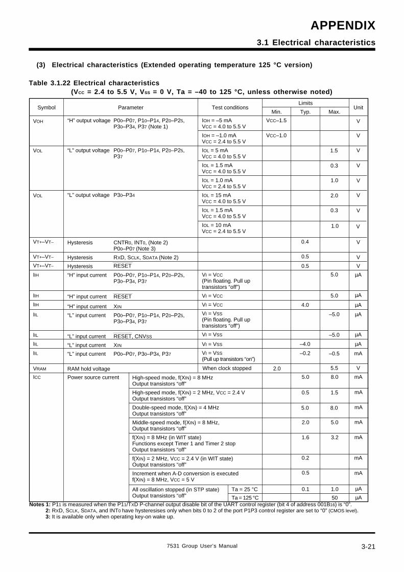
7531 Group User’s Manual 3-21
APPENDIX3.1 Electrical characteristics
(3) Electrical characteristics (Extended operating temperature 125 °C version)
Table 3.1.22 Electrical characteristics(VCC = 2.4 to 5.5 V, V SS = 0 V, Ta = –40 to 125 °C, unless otherwise noted)
Min. Typ. Max.Symbol Parameter
LimitsUnit
IOH = –5 mAVCC = 4.0 to 5.5 V
IOH = –1.0 mAVCC = 2.4 to 5.5 V
IOL = 5 mAVCC = 4.0 to 5.5 V
IOL = 1.5 mAVCC = 4.0 to 5.5 V
IOL = 1.0 mAVCC = 2.4 to 5.5 V
IOL = 15 mAVCC = 4.0 to 5.5 V
IOL = 1.5 mAVCC = 4.0 to 5.5 V
IOL = 10 mAVCC = 2.4 to 5.5 V
VI = VCC(Pin floating. Pull uptransistors “off”)
VI = VCC
VI = VCC
VI = VSS(Pin floating. Pull uptransistors “off”)
VI = VSS
VI = VSS
VI = VSS(Pull up transistors “on”)
Test conditions
VCC–1.5
VCC–1.0
“H” output voltage P00–P07, P10–P14, P20–P25,P30–P34, P37 (Note 1)
“L” output voltage P00–P07, P10–P14, P20–P25,P37
“L” output voltage P30–P34
Hysteresis CNTR0, INT0, (Note 2)P00–P07 (Note 3)
Hysteresis RXD, SCLK, SDATA (Note 2)
Hysteresis
“H” input current P00–P07, P10–P14, P20–P25,P30–P34, P37
“H” input current RESET
“H” input current XIN
“L” input current P00–P07, P10–P14, P20–P25,P30–P34, P37
“L” input current RESET, CNVSS
“L” input current XIN
“L” input current P00–P07, P30–P34, P37
RAM hold voltage
1.5
0.3
1.0
2.0
0.3
V
V
V
V
V
V
V
VOH
VOL
VOL
0.4 VVT+–VT–
V
0.5
0.5
4.0
–4.0
–0.2
5.0
5.0
–5.0
–5.0
–0.5
5.5
V
µA
µA
µA
µA
µA
µA
mA
V
VT+–VT–
VT+–VT–
IIH
IIH
IIH
IIL
IIL
IIL
IIL
VRAM When clock stopped 2.0
RESET
1.0 V
ICC Power source current 5.0
Ta = 25 °C
0.5
5.0
2.0
0.1
1.6
0.2
0.5
8.0
1.5
8.0
5.0
1.0
50
mA
mA
mA
mA
mA
mA
mA
µA
µA
High-speed mode, f(XIN) = 8 MHzOutput transistors “off”
High-speed mode, f(XIN) = 2 MHz, VCC = 2.4 VOutput transistors “off”
Double-speed mode, f(XIN) = 4 MHzOutput transistors “off”
Middle-speed mode, f(XIN) = 8 MHz,Output transistors “off”
f(XIN) = 8 MHz (in WIT state)Functions except Timer 1 and Timer 2 stopOutput transistors “off”
f(XIN) = 2 MHz, VCC = 2.4 V (in WIT state)Output transistors “off”
Increment when A-D conversion is executedf(XIN) = 8 MHz, VCC = 5 V
All oscillation stopped (in STP state)Output transistors “off”
Notes 1: P11 is measured when the P11/TXD P-channel output disable bit of the UART control register (bit 4 of address 001B16) is “0”.2: RXD, SCLK, SDATA, and INT0 have hysteresises only when bits 0 to 2 of the port P1P3 control register are set to “0” (CMOS level).3: It is available only when operating key-on wake up.
3.2
Ta = 125 °C
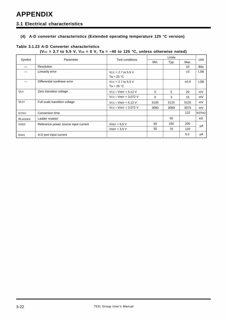
3-22
APPENDIX
7531 Group User’s Manual
3.1 Electrical characteristics
(4) A-D converter characteristics (Extended operating temperature 125 °C version)
Table 3.1.23 A-D Converter characteristics(VCC = 2.7 to 5.5 V, V SS = 0 V, Ta = –40 to 125 °C, unless otherwise noted)
VCC = VREF = 5.12 V
VCC = VREF = 3.072 V
Resolution
Linearity error
Differential nonlinear error
Zero transition voltage
Full scale transition voltage
Conversion time
Ladder resistor
Reference power source input current
A-D port input current
Min. Typ. Max.Symbol Parameter
LimitsUnitTest conditions
VCC = 2.7 to 5.5 VTa = 25 °C
VCC = 2.7 to 5.5 VTa = 25 °C
VCC = VREF = 5.12 V
VCC = VREF = 3.072 V
VREF = 5.0 V
0
0
5105
3060
50
30
5
3
5115
3069
20
15
5125
3075
122
200
55
150
mV
mV
mV
mV
tc(XIN)
kΩ
LSB
LSB
Bits
±0.9
±3
10—
—
—
VOT
VFST
tCONV
RLADDER
IVREF
II(AD) µA5.0
µAVREF = 3.0 V 12070
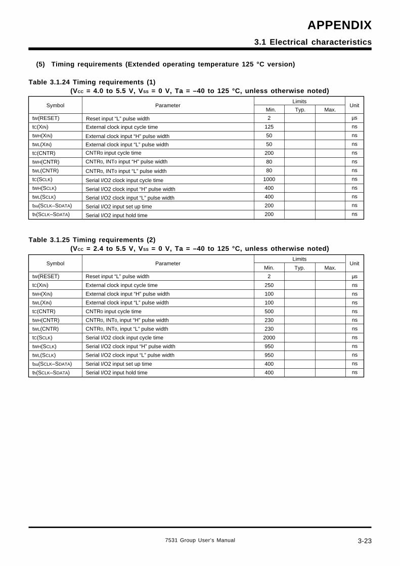
7531 Group User’s Manual 3-23
APPENDIX3.1 Electrical characteristics
(5) Timing requirements (Extended operating temperature 125 °C version)
Table 3.1.24 Timing requirements (1)(VCC = 4.0 to 5.5 V, V SS = 0 V, Ta = –40 to 125 °C, unless otherwise noted)
Min. Typ. Max.Symbol Parameter
LimitsUnit
tW(RESET)
tC(XIN)
tWH(XIN)
tWL(XIN)
tC(CNTR)
tWH(CNTR)
tWL(CNTR)
tC(SCLK)
tWH(SCLK)
tWL(SCLK)
tsu(SCLK–SDATA)
th(SCLK–SDATA)
Reset input “L” pulse width
External clock input cycle time
External clock input “H” pulse width
External clock input “L” pulse width
CNTR0 input cycle time
CNTR0, INT0 input “H” pulse width
CNTR0, INT0 input “L” pulse width
Serial I/O2 clock input cycle time
Serial I/O2 clock input “H” pulse width
Serial I/O2 clock input “L” pulse width
Serial I/O2 input set up time
Serial I/O2 input hold time
2
125
50
50
200
80
80
1000
400
400
200
200
µs
ns
ns
ns
ns
ns
ns
ns
ns
ns
ns
ns
Table 3.1.25 Timing requirements (2)(VCC = 2.4 to 5.5 V, V SS = 0 V, Ta = –40 to 125 °C, unless otherwise noted)
Max.Symbol Parameter Unit
Min. Typ.
Limits
tW(RESET)
tC(XIN)
tWH(XIN)
tWL(XIN)
tC(CNTR)
tWH(CNTR)
tWL(CNTR)
tC(SCLK)
tWH(SCLK)
tWL(SCLK)
tsu(SCLK–SDATA)
th(SCLK–SDATA)
Reset input “L” pulse width
External clock input cycle time
External clock input “H” pulse width
External clock input “L” pulse width
CNTR0 input cycle time
CNTR0, INT0, input “H” pulse width
CNTR0, INT0, input “L” pulse width
Serial I/O2 clock input cycle time
Serial I/O2 clock input “H” pulse width
Serial I/O2 clock input “L” pulse width
Serial I/O2 input set up time
Serial I/O2 input hold time
2
250
100
100
500
230
230
2000
950
950
400
400
µs
ns
ns
ns
ns
ns
ns
ns
ns
ns
ns
ns
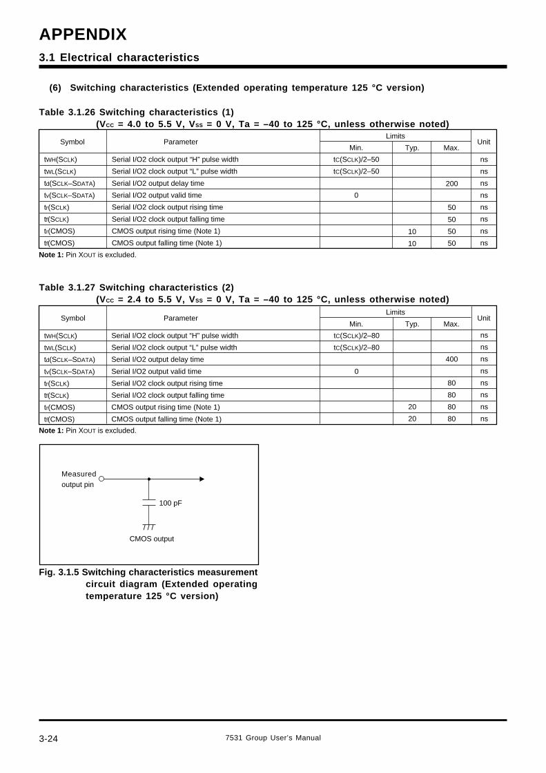
3-24
APPENDIX
7531 Group User’s Manual
3.1 Electrical characteristics
(6) Switching characteristics (Extended operating temperature 125 °C version)
Table 3.1.26 Switching characteristics (1)(VCC = 4.0 to 5.5 V, V SS = 0 V, Ta = –40 to 125 °C, unless otherwise noted)
tC(SCLK)/2–50
tC(SCLK)/2–50
0
Min. Typ. Max.Symbol Parameter
LimitsUnit
tWH(SCLK)
tWL(SCLK)
td(SCLK–SDATA)
tv(SCLK–SDATA)
tr(SCLK)
tf(SCLK)
tr(CMOS)
tf(CMOS)
Serial I/O2 clock output “H” pulse width
Serial I/O2 clock output “L” pulse width
Serial I/O2 output delay time
Serial I/O2 output valid time
Serial I/O2 clock output rising time
Serial I/O2 clock output falling time
CMOS output rising time (Note 1)
CMOS output falling time (Note 1)
200
50
50
50
50
ns
ns
ns
ns
ns
ns
ns
ns
10
10
Note 1: Pin XOUT is excluded.
Table 3.1.27 Switching characteristics (2)(VCC = 2.4 to 5.5 V, V SS = 0 V, Ta = –40 to 125 °C, unless otherwise noted)
Serial I/O2 clock output “H” pulse width
Serial I/O2 clock output “L” pulse width
Serial I/O2 output delay time
Serial I/O2 output valid time
Serial I/O2 clock output rising time
Serial I/O2 clock output falling time
CMOS output rising time (Note 1)
CMOS output falling time (Note 1)
Min. Typ. Max.Symbol Parameter
LimitsUnit
tWH(SCLK)
tWL(SCLK)
td(SCLK–SDATA)
tv(SCLK–SDATA)
tr(SCLK)
tf(SCLK)
tr(CMOS)
tf(CMOS)
tC(SCLK)/2–80
tC(SCLK)/2–80
0
20
20
400
80
80
80
80
ns
ns
ns
ns
ns
ns
ns
ns
Note 1: Pin XOUT is excluded.
Fig. 3.1.5 Switching characteristics measurementcircuit diagram (Extended operatingtemperature 125 °C version)
/ / /
Measuredoutput pin
CMOS output
100 pF
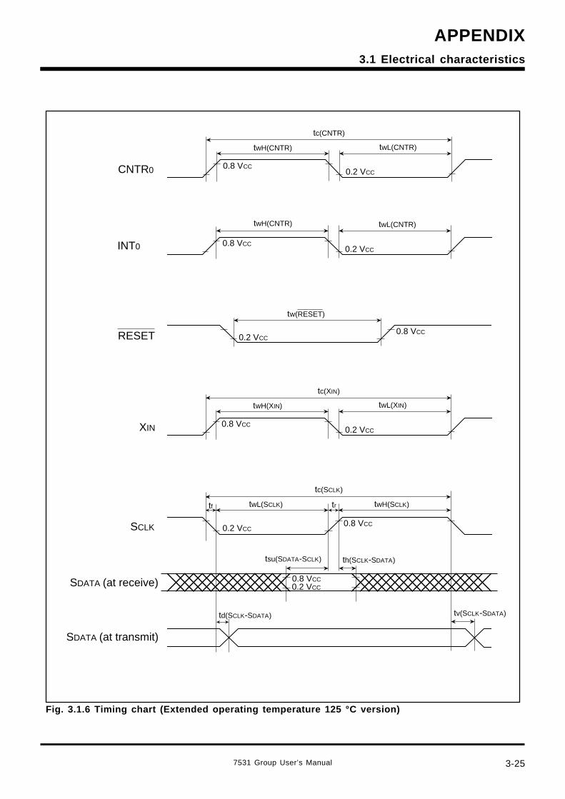
7531 Group User’s Manual 3-25
APPENDIX3.1 Electrical characteristics
Fig. 3.1.6 Timing chart (Extended operating temperature 125 °C version)
0.2 VCC
twL(CNTR)
0.8 VCC
twH(CNTR)
0.2 VCC
0.2 VCC0.8 VCC
0.8 VCC
0.2 VCC
twL(XIN)
0.8 VCC
twH(XIN)
tc(XIN)
XIN
0.2 VCC0.8 VCC
tw(RESET)
RESET
tf tr
0.2 VCC
twL(CNTR)
0.8 VCC
twH(CNTR)
tc(CNTR)
td(SCLK-SDATA) tv(SCLK-SDATA)
tc(SCLK)
twL(SCLK) twH(SCLK)
th(SCLK-SDATA)tsu(SDATA-SCLK)
SDATA (at transmit)
SDATA (at receive)
SCLK
INT0
CNTR0
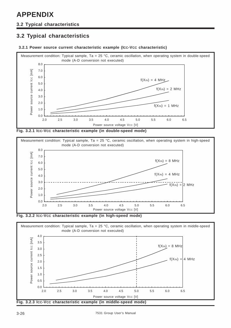
3-26
APPENDIX
7531 Group User’s Manual
3.2 Typical characteristics
0.0
0.5
1.0
1.5
2.0
2.5
3.0
3.5
4.0
2.0 2.5 3.0 3.5 4.0 4.5 5.0 5.5 6.0 6.5
0.0
1.0
2.0
3.0
4.0
5.0
6.0
7.0
8.0
2.0 2.5 3.0 3.5 4.0 4.5 5.0 5.5 6.0 6.5
0.0
1.0
2.0
3.0
4.0
5.0
6.0
7.0
8.0
2.0 2.5 3.0 3.5 4.0 4.5 5.0 5.5 6.0 6.5
3.2 Typical characteristics
3.2.1 Power source current characteristic example (ICC-VCC characteristic)
Fig. 3.2.1 ICC-VCC characteristic example (in double-speed mode)
Fig. 3.2.2 ICC-VCC characteristic example (in high-speed mode)
Measurement condition: Typical sample, Ta = 25 °C, ceramic oscillation, when operating system in double-speedmode (A-D conversion not executed)
f(XIN) = 4 MHz
f(XIN) = 2 MHz
f(XIN) = 1 MHz
Power source voltage VCC [V]
Po
we
r so
urc
e c
urr
en
t I C
C [
mA
]
f(XIN) = 8 MHz
f(XIN) = 4 MHz
f(XIN) = 2 MHz
Power source voltage VCC [V]
Po
we
r so
urc
e c
urr
en
t I C
C [
mA
]
Measurement condition: Typical sample, Ta = 25 °C, ceramic oscillation, when operating system in high-speedmode (A-D conversion not executed)
Fig. 3.2.3 ICC-VCC characteristic example (in middle-speed mode)
f(XIN) = 8 MHz
f(XIN) = 4 MHz
Power source voltage VCC [V]
Po
we
r so
urc
e c
urr
en
t I C
C [
mA
]
Measurement condition: Typical sample, Ta = 25 °C, ceramic oscillation, when operating system in middle-speedmode (A-D conversion not executed)
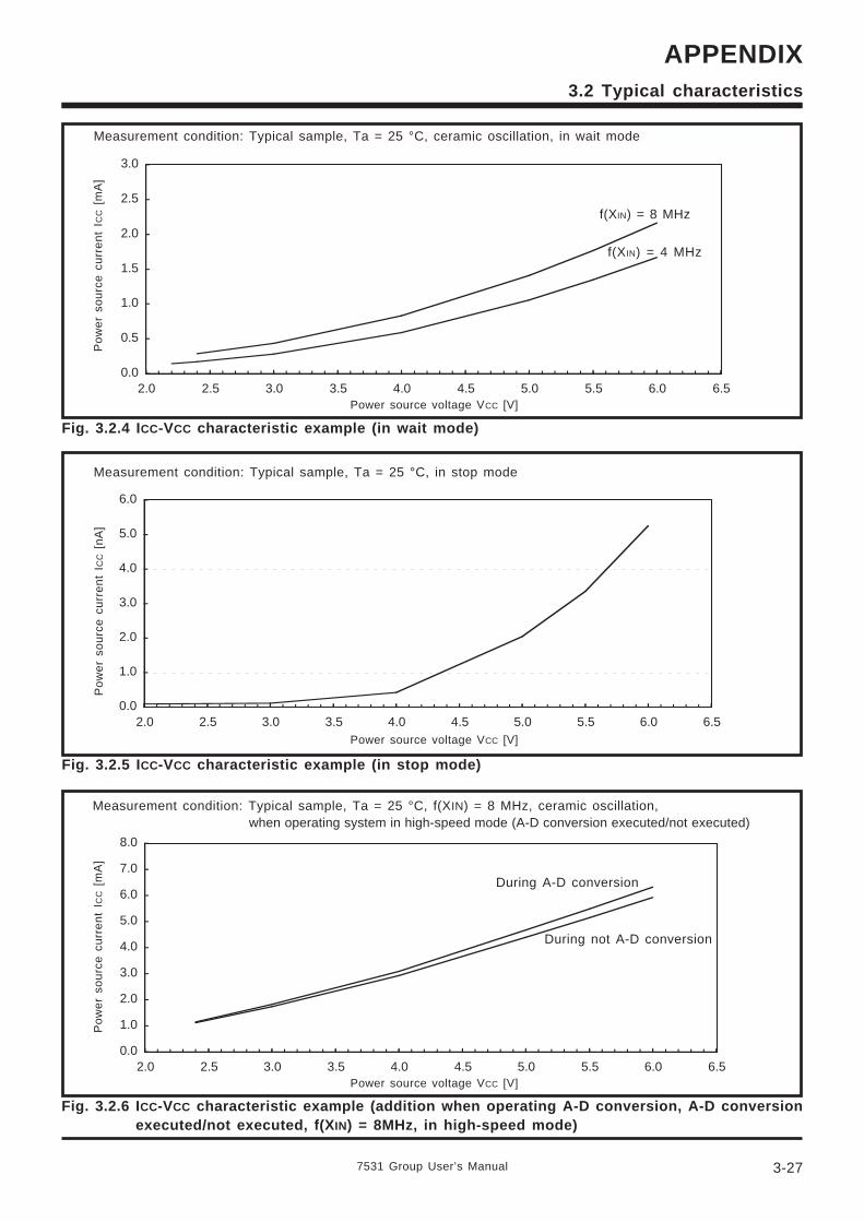
7531 Group User’s Manual 3-27
APPENDIX3.2 Typical characteristics
0.0
0.5
1.0
1.5
2.0
2.5
3.0
2.0 2.5 3.0 3.5 4.0 4.5 5.0 5.5 6.0 6.5
0.0
1.0
2.0
3.0
4.0
5.0
6.0
7.0
8.0
2.0 2.5 3.0 3.5 4.0 4.5 5.0 5.5 6.0 6.5
0.0
1.0
2.0
3.0
4.0
5.0
6.0
2.0 2.5 3.0 3.5 4.0 4.5 5.0 5.5 6.0 6.5
Fig. 3.2.4 ICC-VCC characteristic example (in wait mode)
Fig. 3.2.5 ICC-VCC characteristic example (in stop mode)
Fig. 3.2.6 ICC-VCC characteristic example (addition when operating A-D conversion, A-D conversionexecuted/not executed, f(XIN) = 8MHz, in high-speed mode)
Measurement condition: Typical sample, Ta = 25 °C, ceramic oscillation, in wait mode
Power source voltage VCC [V]
Po
we
r so
urc
e c
urr
en
t I C
C [
mA
]
f(XIN) = 8 MHz
f(XIN) = 4 MHz
Measurement condition: Typical sample, Ta = 25 °C, in stop mode
Power source voltage VCC [V]
Po
we
r so
urc
e c
urr
en
t I C
C [
nA
]
Power source voltage VCC [V]
Po
we
r so
urc
e c
urr
en
t I C
C [
mA
]
Measurement condition: Typical sample, Ta = 25 °C, f(XIN) = 8 MHz, ceramic oscillation,when operating system in high-speed mode (A-D conversion executed/not executed)
During A-D conversion
During not A-D conversion
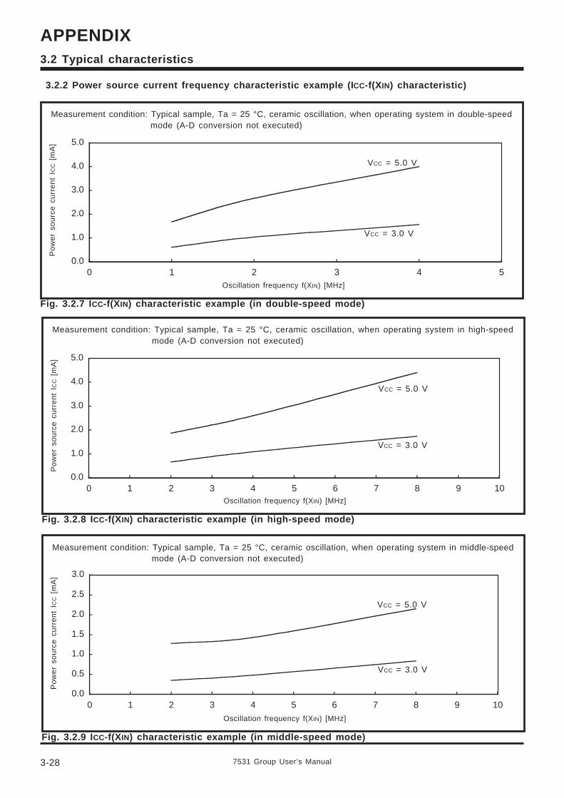
3-28
APPENDIX
7531 Group User’s Manual
3.2 Typical characteristics
0.0
0.5
1.0
1.5
2.0
2.5
3.0
0 1 2 3 4 5 6 7 8 9 10
0.0
1.0
2.0
3.0
4.0
5.0
0 1 2 3 4 5 6 7 8 9 10
0.0
1.0
2.0
3.0
4.0
5.0
0 1 2 3 4 5
3.2.2 Power source current frequency characteristic example (ICC-f(XIN) characteristic)
Fig. 3.2.7 ICC-f(XIN) characteristic example (in double-speed mode)
Measurement condition: Typical sample, Ta = 25 °C, ceramic oscillation, when operating system in double-speedmode (A-D conversion not executed)
VCC = 3.0 V
VCC = 5.0 V
Oscillation frequency f(XIN) [MHz]
Po
we
r so
urc
e c
urr
en
t I C
C [
mA
]
Fig. 3.2.8 ICC-f(XIN) characteristic example (in high-speed mode)
Measurement condition: Typical sample, Ta = 25 °C, ceramic oscillation, when operating system in high-speedmode (A-D conversion not executed)
VCC = 3.0 V
VCC = 5.0 V
Oscillation frequency f(XIN) [MHz]
Po
we
r so
urc
e c
urr
en
t I C
C [
mA
]
Fig. 3.2.9 ICC-f(XIN) characteristic example (in middle-speed mode)
Measurement condition: Typical sample, Ta = 25 °C, ceramic oscillation, when operating system in middle-speedmode (A-D conversion not executed)
VCC = 3.0 V
VCC = 5.0 V
Oscillation frequency f(XIN) [MHz]
Po
we
r so
urc
e c
urr
en
t I C
C [
mA
]
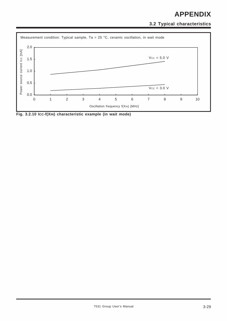
7531 Group User’s Manual 3-29
APPENDIX3.2 Typical characteristics
0.0
0.5
1.0
1.5
2.0
0 1 2 3 4 5 6 7 8 9 10
Measurement condition: Typical sample, Ta = 25 °C, ceramic oscillation, in wait mode
VCC = 3.0 V
VCC = 5.0 V
Oscillation frequency f(XIN) [MHz]
Po
we
r so
urc
e c
urr
en
t I C
C [
mA
]
Fig. 3.2.10 ICC-f(XIN) characteristic example (in wait mode)
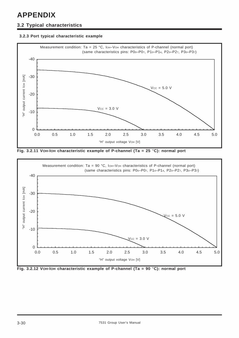
3-30
APPENDIX
7531 Group User’s Manual
3.2 Typical characteristics
-40
-30
-20
-10
00.0 0.5 1.0 1.5 2.0 2.5 3.0 3.5 4.0 4.5 5.0
-40
-30
-20
-10
00.0 0.5 1.0 1.5 2.0 2.5 3.0 3.5 4.0 4.5 5.0
3.2.3 Port typical characteristic example
Fig. 3.2.11 VOH-IOH characteristic example of P-channel (Ta = 25 °C): normal port
Fig. 3.2.12 VOH-IOH characteristic example of P-channel (Ta = 90 °C): normal port
Measurement condition: Ta = 25 °C, IOH–VOH characteristics of P-channel (normal port)(same characteristics pins: P00–P07, P10–P14, P20–P27, P30–P37)
“H” output voltage VOH [V]
“H”
ou
tpu
t cu
rre
nt
I OH
[m
A]
VCC = 3.0 V
Measurement condition: Ta = 90 °C, IOH–VOH characteristics of P-channel (normal port)(same characteristics pins: P00–P07, P10–P14, P20–P27, P30–P37)
VCC = 5.0 V
“H” output voltage VOH [V]
“H”
ou
tpu
t cu
rre
nt
I OH
[m
A]
VCC = 3.0 V
VCC = 5.0 V
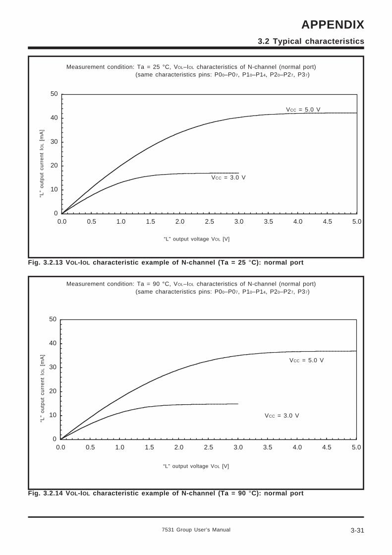
7531 Group User’s Manual 3-31
APPENDIX3.2 Typical characteristics
0
10
20
30
40
50
0.0 0.5 1.0 1.5 2.0 2.5 3.0 3.5 4.0 4.5 5.0
0
10
20
30
40
50
0.0 0.5 1.0 1.5 2.0 2.5 3.0 3.5 4.0 4.5 5.0
Fig. 3.2.13 VOL-IOL characteristic example of N-channel (Ta = 25 °C): normal port
Fig. 3.2.14 VOL-IOL characteristic example of N-channel (Ta = 90 °C): normal port
Measurement condition: Ta = 25 °C, VOL–IOL characteristics of N-channel (normal port)(same characteristics pins: P00–P07, P10–P14, P20–P27, P37)
VCC = 5.0 V
“L” output voltage VOL [V]
“L”
ou
tpu
t cu
rre
nt
I OL [
mA
]
VCC = 3.0 V
Measurement condition: Ta = 90 °C, VOL–IOL characteristics of N-channel (normal port)(same characteristics pins: P00–P07, P10–P14, P20–P27, P37)
VCC = 5.0 V
“L” output voltage VOL [V]
“L”
ou
tpu
t cu
rre
nt
I OL [
mA
]
VCC = 3.0 V
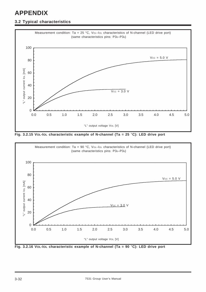
3-32
APPENDIX
7531 Group User’s Manual
3.2 Typical characteristics
0
20
40
60
80
100
0.0 0.5 1.0 1.5 2.0 2.5 3.0 3.5 4.0 4.5 5.0
0
20
40
60
80
100
0.0 0.5 1.0 1.5 2.0 2.5 3.0 3.5 4.0 4.5 5.0
Fig. 3.2.15 VOL-IOL characteristic example of N-channel (Ta = 25 °C): LED drive port
Fig. 3.2.16 VOL-IOL characteristic example of N-channel (Ta = 90 °C): LED drive port
Measurement condition: Ta = 25 °C, VOL–IOL characteristics of N-channel (LED drive port)(same characteristics pins: P30–P36)
VCC = 5.0 V
“L” output voltage VOL [V]
“L”
ou
tpu
t cu
rre
nt
I OL [
mA
]
VCC = 3.0 V
Measurement condition: Ta = 90 °C, VOL–IOL characteristics of N-channel (LED drive port)(same characteristics pins: P30–P36)
VCC = 5.0 V
“L” output voltage VOL [V]
“L”
ou
tpu
t cu
rre
nt
I OL [
mA
]
VCC = 3.0 V
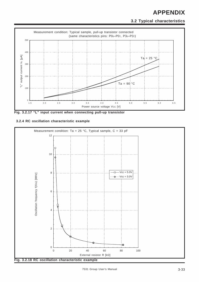
7531 Group User’s Manual 3-33
APPENDIX3.2 Typical characteristics
-500
-400
-300
-200
-100
01 .5 2 .0 2 .5 3 .0 3 .5 4 .0 4 .5 5 .0 5 .5 6 .0 6 .5
0
2
4
6
8
10
12
0 20 40 60 80 100
Vcc = 5.0V
Vcc = 3.0V
Fig. 3.2.17 “L” input current when connecting pull-up transistor
3.2.4 RC oscillation characteristic example
Measurement condition: Typical sample, pull-up transistor connected(same characteristics pins: P00–P07, P30–P37)
Ta = 25 °C
Ta = 90 °C
Power source voltage VCC [V]
“L”
ou
tpu
t cu
rre
nt
I IL [
µA]
Fig. 3.2.18 RC oscillation characteristic example
Measurement condition: Ta = 25 °C, Typical sample, C = 33 pF
External resistor R [kΩ]
Osc
illa
tion
fre
qu
en
cy f
(XIN
) [M
Hz]
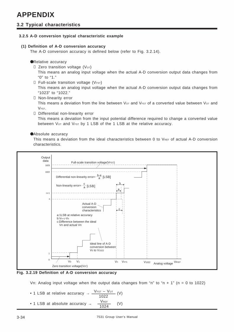
3-34
APPENDIX
7531 Group User’s Manual
3.2 Typical characteristics
3.2.5 A-D conversion typical characteristic example
(1) Definition of A-D conversion accuracyThe A-D conversion accuracy is defined below (refer to Fig. 3.2.14).
Relative accuracy➀ Zero transition voltage (VOT)
This means an analog input voltage when the actual A-D conversion output data changes from“0” to “1.”
➁ Full-scale transition voltage (VFST)This means an analog input voltage when the actual A-D conversion output data changes from“1023” to “1022.”
➂ Non-linearity errorThis means a deviation from the line between VOT and VFST of a converted value between VOT andVFST.
➃ Differential non-linearity errorThis means a deviation from the input potential difference required to change a converted valuebetween VOT and VFST by 1 LSB of the 1 LSB at the relative accuracy.
Absolute accuracyThis means a deviation from the ideal characteristics between 0 to VREF of actual A-D conversioncharacteristics.
VREF
1024
Fig. 3.2.19 Definition of A-D conversion accuracy
Vn: Analog input voltage when the output data changes from “n” to “n + 1” (n = 0 to 1022)
• 1 LSB at relative accuracy → (V)
• 1 LSB at absolute accuracy → (V)
VFST – VOT
1022
Analog voltage VREFV1022VnV1V0
Zero transition voltage(V0T)
Full-scale transition voltage(VFST)
Non-linearity error=
Actual A-Dconversion characteristics
Vn+1
n+1
n
1022
1023
1
0
Ideal line of A-Dconversion betweenV0 to V1022
Outputdata
b
a
a:1LSB at relative accuracyb:Vn+1-Vn
c:Difference between the ideal Vn and actual Vn
Differential non-linearity error= b-aa [LSB]
c
ca [LSB]
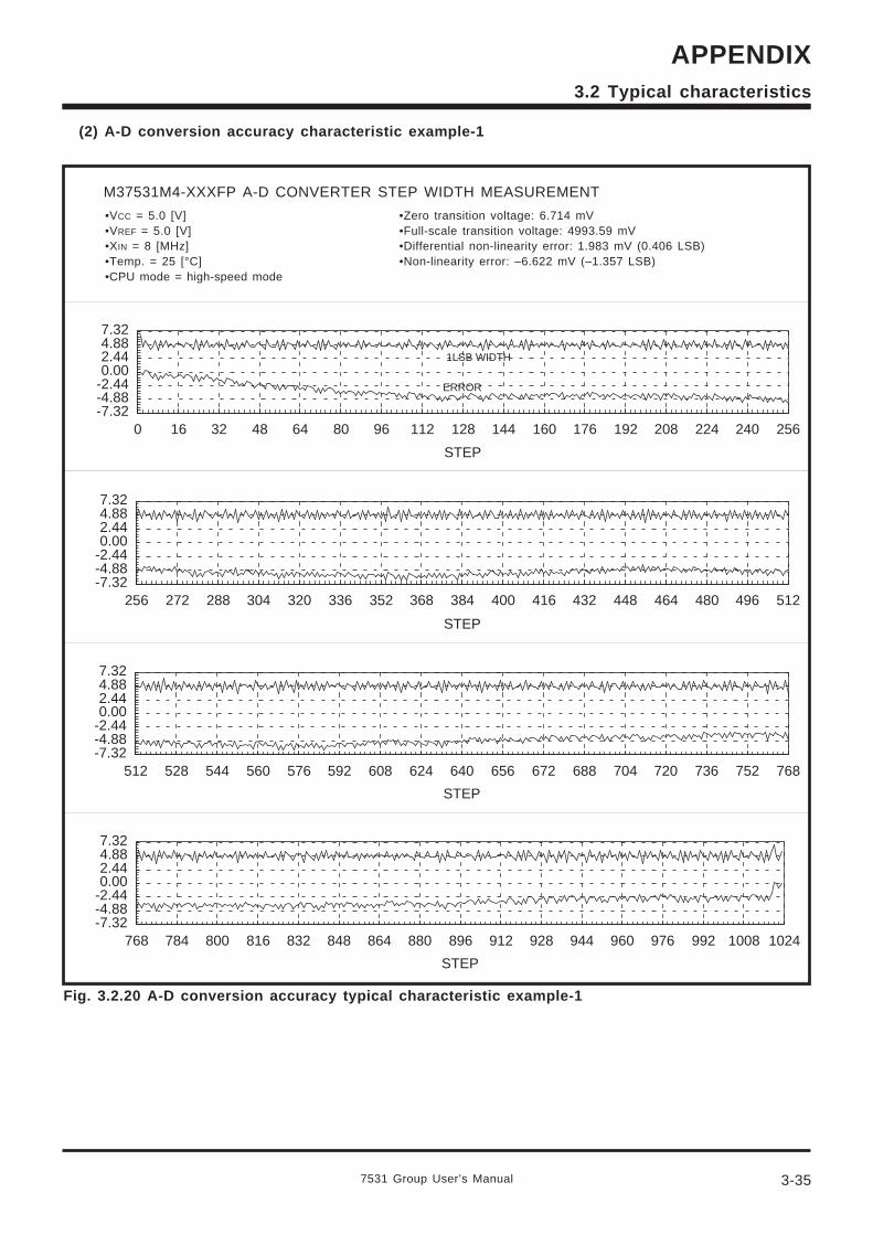
7531 Group User’s Manual 3-35
APPENDIX3.2 Typical characteristics
-7.32-4.88-2.440.002.444.887.32
0 16 32 48 64 80 96 112 128 144 160 176 192 208 224 240 256
STEP
1LSB WIDTH
ERROR
-7.32-4.88-2.440.002.444.887.32
256 272 288 304 320 336 352 368 384 400 416 432 448 464 480 496 512
STEP
-7.32-4.88-2.440.002.444.887.32
512 528 544 560 576 592 608 624 640 656 672 688 704 720 736 752 768
STEP
-7.32-4.88-2.440.002.444.887.32
768 784 800 816 832 848 864 880 896 912 928 944 960 976 992 1008 1024
STEP
Fig. 3.2.20 A-D conversion accuracy typical characteristic example-1
•VCC = 5.0 [V]•VREF = 5.0 [V]•XIN = 8 [MHz]•Temp. = 25 [°C]•CPU mode = high-speed mode
M37531M4-XXXFP A-D CONVERTER STEP WIDTH MEASUREMENT
(2) A-D conversion accuracy characteristic example-1
•Zero transition voltage: 6.714 mV•Full-scale transition voltage: 4993.59 mV•Differential non-linearity error: 1.983 mV (0.406 LSB)•Non-linearity error: –6.622 mV (–1.357 LSB)
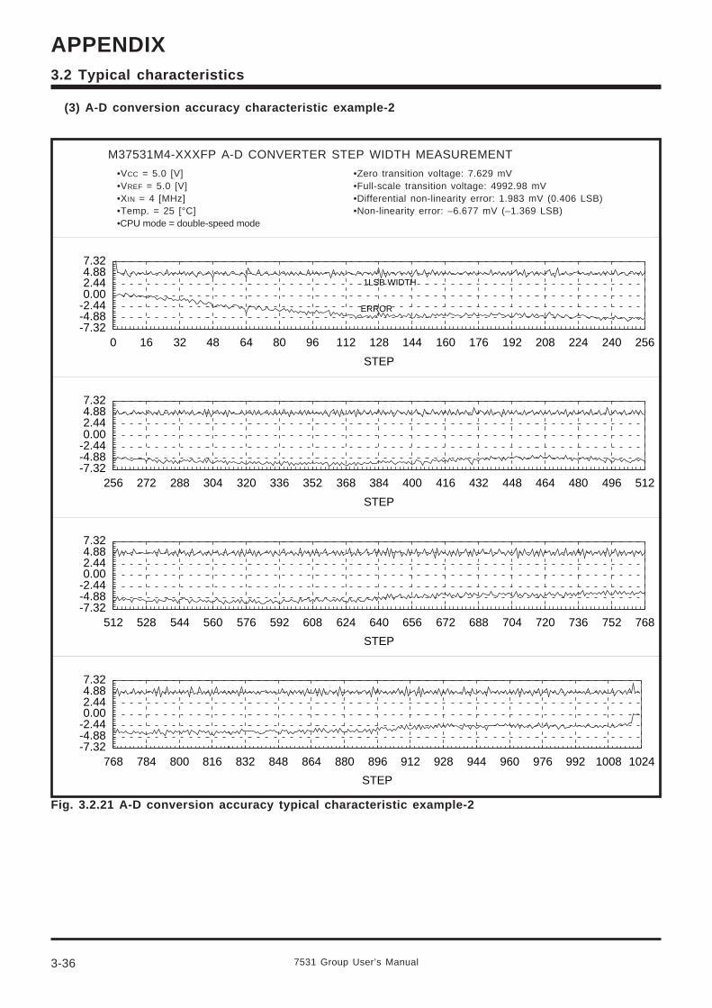
3-36
APPENDIX
7531 Group User’s Manual
3.2 Typical characteristics
-7.32-4.88-2.440.002.444.887.32
0 16 32 48 64 80 96 112 128 144 160 176 192 208 224 240 256
STEP
1LSB WIDTH
ERROR
-7.32-4.88-2.440.002.444.887.32
256 272 288 304 320 336 352 368 384 400 416 432 448 464 480 496 512
STEP
-7.32-4.88-2.440.002.444.887.32
512 528 544 560 576 592 608 624 640 656 672 688 704 720 736 752 768
STEP
-7.32-4.88-2.440.002.444.887.32
768 784 800 816 832 848 864 880 896 912 928 944 960 976 992 1008 1024
STEP
Fig. 3.2.21 A-D conversion accuracy typical characteristic example-2
•VCC = 5.0 [V]•VREF = 5.0 [V]•XIN = 4 [MHz]•Temp. = 25 [°C]•CPU mode = double-speed mode
•Zero transition voltage: 7.629 mV•Full-scale transition voltage: 4992.98 mV•Differential non-linearity error: 1.983 mV (0.406 LSB)•Non-linearity error: –6.677 mV (–1.369 LSB)
M37531M4-XXXFP A-D CONVERTER STEP WIDTH MEASUREMENT
(3) A-D conversion accuracy characteristic example-2
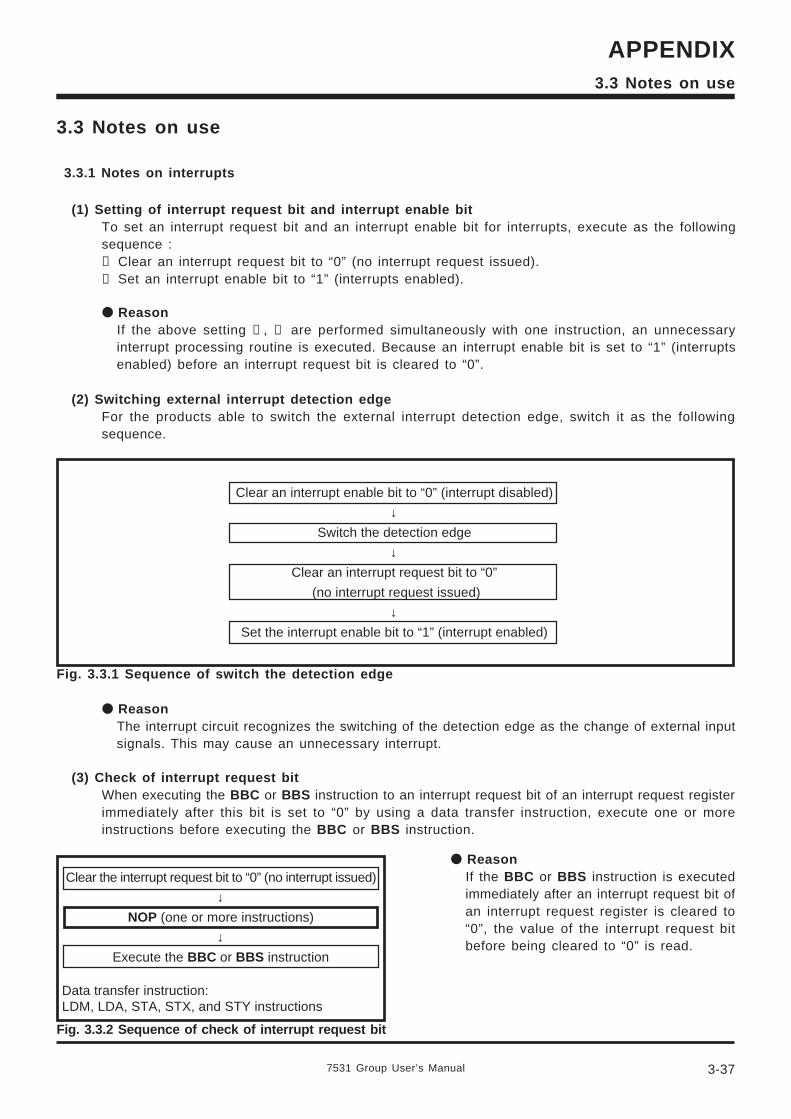
7531 Group User’s Manual 3-37
APPENDIX
3.3 Notes on use
3.3.1 Notes on interrupts
(1) Setting of interrupt request bit and interrupt enable bitTo set an interrupt request bit and an interrupt enable bit for interrupts, execute as the followingsequence :➀ Clear an interrupt request bit to “0” (no interrupt request issued).➁ Set an interrupt enable bit to “1” (interrupts enabled).
ReasonIf the above setting ➀, ➁ are performed simultaneously with one instruction, an unnecessaryinterrupt processing routine is executed. Because an interrupt enable bit is set to “1” (interruptsenabled) before an interrupt request bit is cleared to “0”.
(2) Switching external interrupt detection edgeFor the products able to switch the external interrupt detection edge, switch it as the followingsequence.
Clear an interrupt enable bit to “0” (interrupt disabled)
↓Switch the detection edge
↓Clear an interrupt request bit to “0”
(no interrupt request issued)
↓Set the interrupt enable bit to “1” (interrupt enabled)
3.3 Notes on use
Fig. 3.3.1 Sequence of switch the detection edge
ReasonThe interrupt circuit recognizes the switching of the detection edge as the change of external inputsignals. This may cause an unnecessary interrupt.
(3) Check of interrupt request bitWhen executing the BBC or BBS instruction to an interrupt request bit of an interrupt request registerimmediately after this bit is set to “0” by using a data transfer instruction, execute one or moreinstructions before executing the BBC or BBS instruction.
Clear the interrupt request bit to “0” (no interrupt issued)
↓NOP (one or more instructions)
↓Execute the BBC or BBS instruction
Data transfer instruction:LDM, LDA, STA, STX, and STY instructions
ReasonIf the BBC or BBS instruction is executedimmediately after an interrupt request bit ofan interrupt request register is cleared to“0”, the value of the interrupt request bitbefore being cleared to “0” is read.
Fig. 3.3.2 Sequence of check of interrupt request bit
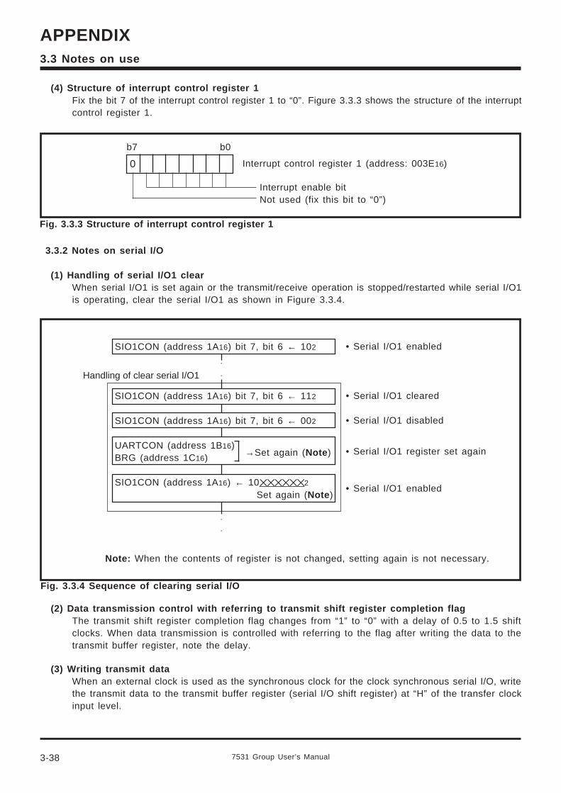
3-38
APPENDIX
7531 Group User’s Manual
(4) Structure of interrupt control register 1Fix the bit 7 of the interrupt control register 1 to “0”. Figure 3.3.3 shows the structure of the interruptcontrol register 1.
Fig. 3.3.3 Structure of interrupt control register 1
3.3 Notes on use
3.3.2 Notes on serial I/O
(1) Handling of serial I/O1 clearWhen serial I/O1 is set again or the transmit/receive operation is stopped/restarted while serial I/O1is operating, clear the serial I/O1 as shown in Figure 3.3.4.
Fig. 3.3.4 Sequence of clearing serial I/O
0
b7 b0
Interrupt control register 1 (address: 003E16)
Interrupt enable bitNot used (fix this bit to “0”)
→Set again (Note )
• Serial I/O1 enabled
• Serial I/O1 cleared
• Serial I/O1 disabled
• Serial I/O1 register set again
• Serial I/O1 enabled
Handling of clear serial I/O1
Note: When the contents of register is not changed, setting again is not necessary.
(2) Data transmission control with referring to transmit shift register completion flagThe transmit shift register completion flag changes from “1” to “0” with a delay of 0.5 to 1.5 shiftclocks. When data transmission is controlled with referring to the flag after writing the data to thetransmit buffer register, note the delay.
(3) Writing transmit dataWhen an external clock is used as the synchronous clock for the clock synchronous serial I/O, writethe transmit data to the transmit buffer register (serial I/O shift register) at “H” of the transfer clockinput level.
SIO1CON (address 1A16) bit 7, bit 6 ← 102
SIO1CON (address 1A16) bit 7, bit 6 ← 112
SIO1CON (address 1A16) bit 7, bit 6 ← 002
UARTCON (address 1B16)BRG (address 1C16)
SIO1CON (address 1A16) ← 102
Set again (Note )
7531 Group User’s Manual 3-39
APPENDIX
(4) Serial I/O2 transmit/receive shift completion flag•The transmit/receive shift completion flag of the serial I/O2 control register is set to “1” after completingtransmit/receive shift. In order to set this flag to “0”, write data (dummy data at reception) to theserial I/O2 register by program.
•Bit 7 of the serial I/O2 control register is set to “1” a half cycle (of the shift clock) earlier thancompletion of shift operation. Accordingly, when using this bit to confirm shift completion, a halfcycle or more of the shift clock must pass after confirming that this bit is set to “1”, before performingread/write to the serial I/O2 register.
3.3.3 Notes on A-D converter
(1) Analog input pinMake the signal source impedance for analog input low, or equip an analog input pin with an externalcapacitor of 0.01µF to 1µF. Further, be sure to verify the operation of application products on theuser side.
ReasonAn analog input pin includes the capacitor for analog voltage comparison. Accordingly, whensignals from signal source with high impedance are input to an analog input pin, charge anddischarge noise generates. This may cause the A-D conversion precision to be worse.
(2) Clock frequency during A-D conversionThe comparator consists of a capacity coupling, and a charge of the capacity will be lost if the clockfrequency is too low. Thus, make sure the following during an A-D conversion.• f(XIN) is 500 kHz or more• Do not execute the STP instruction
3.3.4 Notes on RESET pin
(1) Connecting capacitorIn case where the RESET signal rise time is long, connect a ceramic capacitor or others across theRESET pin and the VSS pin. And use a 1000 pF or more capacitor for high frequency use. Whenconnecting the capacitor, note the following :• Make the length of the wiring which is connected to a capacitor as short as possible.• Be sure to verify the operation of application products on the user side.
ReasonIf the several nanosecond or several ten nanosecond impulse noise enters the RESET pin, it maycause a microcomputer failure.
3.3 Notes on use
3-40
APPENDIX
7531 Group User’s Manual
3.3.5 Notes on input and output pins
(1) Notes in stand-by stateIn stand-by state*1 for low-power dissipation, do not make input levels of an input port and an I/Oport “undefined”.Pull-up (connect the port to VCC) or pull-down (connect the port to VSS) these ports through aresistor.When determining a resistance value, note the following points:• External circuit• Variation of output levels during the ordinary operation
When using built-in pull-up or pull-down resistor, note on varied current values:• When setting as an input port : Fix its input level• When setting as an output port : Prevent current from flowing out to external
ReasonThe output transistor becomes the OFF state, which causes the ports to be the high-impedancestate. Note that the level becomes “undefined” depending on external circuits.Accordingly, the potential which is input to the input buffer in a microcomputer is unstable in thestate that input levels of a input port and an I/O port are “undefined”. This may cause powersource current.
*1 stand-by state : the stop mode by executing the STP instructionthe wait mode by executing the WIT instruction
(2) Modifying output data with bit managing instructionWhen the port latch of an I/O port is modified with the bit managing instruction*2, the value of theunspecified bit may be changed.
ReasonThe bit managing instructions are read-modify-write form instructions for reading and writing databy a byte unit. Accordingly, when these instructions are executed on a bit of the port latch of anI/O port, the following is executed to all bits of the port latch.• As for a bit which is set for an input port :
The pin state is read in the CPU, and is written to this bit after bit managing.• As for a bit which is set for an output port :
The bit value of the port latch is read in the CPU, and is written to this bit after bit managing.
Note the following :• Even when a port which is set as an output port is changed for an input port, its port latch holds
the output data.• As for a bit of the port latch which is set for an input port, its value may be changed even when
not specified with a bit managing instruction in case where the pin state differs from its port latchcontents.
*2 bit managing instructions : SEB , and CLB instructions
3.3 Notes on use
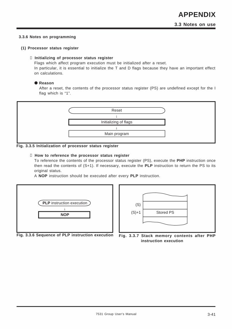
7531 Group User’s Manual 3-41
APPENDIX
3.3.6 Notes on programming
(1) Processor status register
➀ Initializing of processor status registerFlags which affect program execution must be initialized after a reset.In particular, it is essential to initialize the T and D flags because they have an important effecton calculations.
ReasonAfter a reset, the contents of the processor status register (PS) are undefined except for the Iflag which is “1”.
Reset
↓Initializing of flags
↓Main program
Fig. 3.3.7 Stack memory contents after PHPinstruction execution
PLP instruction execution
↓NOP
➁ How to reference the processor status registerTo reference the contents of the processor status register (PS), execute the PHP instruction oncethen read the contents of (S+1). If necessary, execute the PLP instruction to return the PS to itsoriginal status.A NOP instruction should be executed after every PLP instruction.
Fig. 3.3.5 Initialization of processor status register
Fig. 3.3.6 Sequence of PLP instruction execution
3.3 Notes on use
(S)
(S)+1 Stored PS
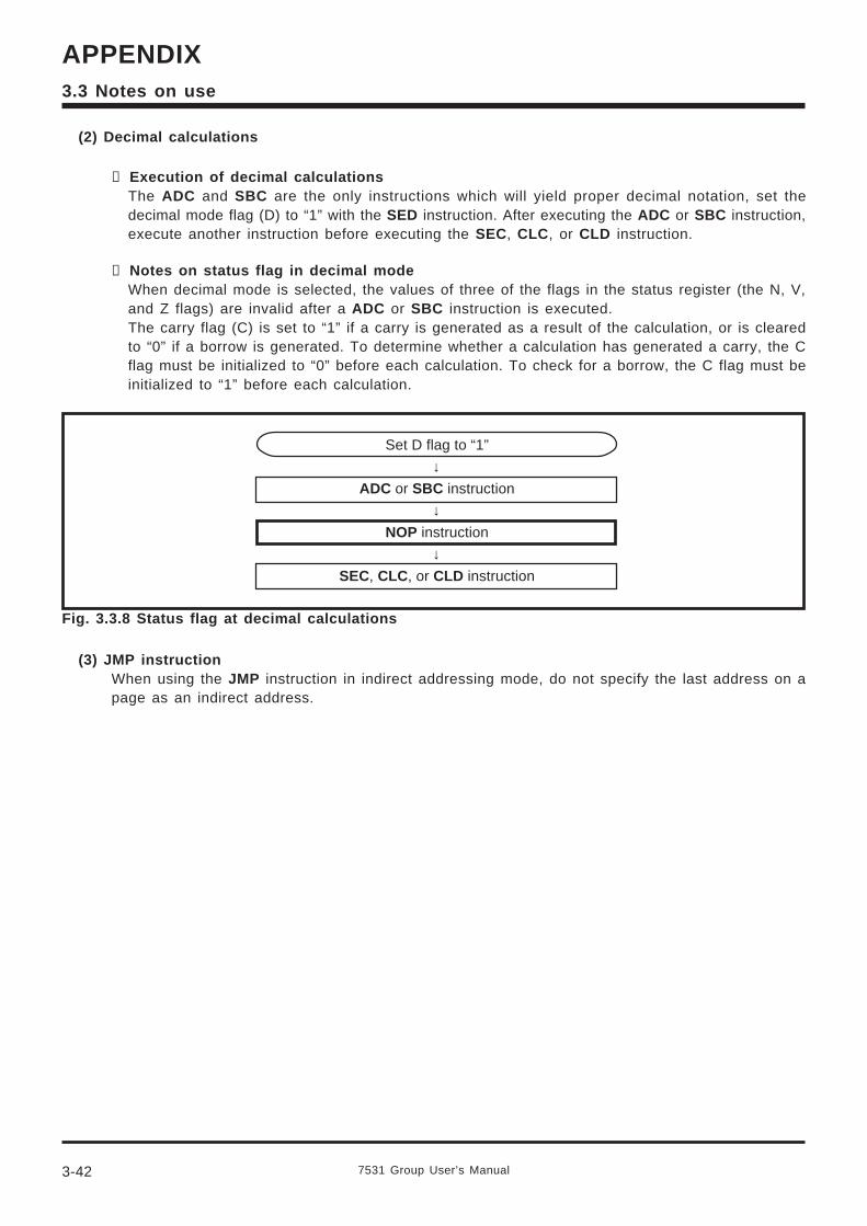
3-42
APPENDIX
7531 Group User’s Manual
(2) Decimal calculations
➀ Execution of decimal calculationsThe ADC and SBC are the only instructions which will yield proper decimal notation, set thedecimal mode flag (D) to “1” with the SED instruction. After executing the ADC or SBC instruction,execute another instruction before executing the SEC, CLC , or CLD instruction.
➁ Notes on status flag in decimal modeWhen decimal mode is selected, the values of three of the flags in the status register (the N, V,and Z flags) are invalid after a ADC or SBC instruction is executed.The carry flag (C) is set to “1” if a carry is generated as a result of the calculation, or is clearedto “0” if a borrow is generated. To determine whether a calculation has generated a carry, the Cflag must be initialized to “0” before each calculation. To check for a borrow, the C flag must beinitialized to “1” before each calculation.
(3) JMP instructionWhen using the JMP instruction in indirect addressing mode, do not specify the last address on apage as an indirect address.
Set D flag to “1”
↓ADC or SBC instruction
↓NOP instruction
↓SEC, CLC, or CLD instruction
Fig. 3.3.8 Status flag at decimal calculations
3.3 Notes on use
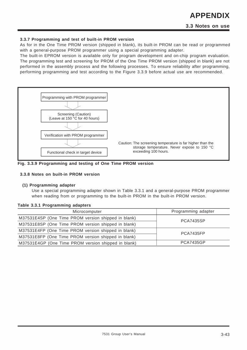
7531 Group User’s Manual 3-43
APPENDIX
Fig. 3.3.9 Programming and testing of One Time PROM version
3.3.7 Programming and test of built-in PROM versionAs for in the One Time PROM version (shipped in blank), its built-in PROM can be read or programmedwith a general-purpose PROM programmer using a special programming adapter.The built-in EPROM version is available only for program development and on-chip program evaluation.The programming test and screening for PROM of the One Time PROM version (shipped in blank) are notperformed in the assembly process and the following processes. To ensure reliability after programming,performing programming and test according to the Figure 3.3.9 before actual use are recommended.
3.3.8 Notes on built-in PROM version
(1) Programming adapterUse a special programming adapter shown in Table 3.3.1 and a general-purpose PROM programmerwhen reading from or programming to the built-in PROM in the built-in PROM version.
Table 3.3.1 Programming adapters
M37531E4SP (One Time PROM version shipped in blank)
M37531E8SP (One Time PROM version shipped in blank)
M37531E4FP (One Time PROM version shipped in blank)
M37531E8FP (One Time PROM version shipped in blank)
M37531E4GP (One Time PROM version shipped in blank)
PCA7435SP
PCA7435FP
PCA7435GP
Programming adapterMicrocomputer
3.3 Notes on use
Programming with PROM programmer
Screening (Caution)(Leave at 150 °C for 40 hours)
Verification with PROM programmer
Functional check in target device
Caution: The screening temperature is far higher than the storage temperature. Never expose to 150 °C exceeding 100 hours.
3-44
APPENDIX
7531 Group User’s Manual
(2) Programming/readingIn PROM mode, operation is the same as that of the M5M27C101AK, but programming conditionsof PROM programmer are not set automatically because there are no internal device ID codes.Accurately set the following conditions for data programming /reading. Take care not to apply 21 Vto VPP pin (is also used as the CNVSS pin), or the product may be permanently damaged.• Programming voltage: 12.5 V• Setting of PROM programmer switch: refer to Table 3.3.2.
Product name format PROM programmerstart address
Address 0E08016 (Note 1 )
Address 0C08016 (Note 2 )
PROM programmerend address
M37531E4SP
M37531E4FP
M37531E4GP
M37531E8SP
M37531E8FP
Table 3.3.2 PROM programmer address setting
Address 0FFFD16 (Note 1 )
Address 0FFFD16 (Note 2 )
Notes 1: Addersses E08016 to FFFD16 in the built-in PROM corresponds to addresses 0E08016 to 0FFFD16
in the PROM programmer.2: Addersses C08016 to FFFD16 in the built-in PROM corresponds to addresses 0C08016 to 0FFFD16
in the PROM programmer.
3.3 Notes on use
7531 Group User’s Manual 3-45
APPENDIX
3.3.9 Termination of unused pins
(1) Terminate unused pins
➀ Output ports : Open
➁ Input ports :Connect each pin to VCC or VSS through each resistor of 1 kΩ to 10 kΩ.Ports that permit the selecting of a built-in pull-up or pull-down resistor can also use this resistor.As for pins whose potential affects to operation modes such as pins CNVSS, INT or others, selectthe VCC pin or the VSS pin according to their operation mode.
➂ I/O ports :• Set the I/O ports for the input mode and connect them to VCC or VSS through each resistor of
1 kΩ to 10 kΩ.Ports that permit the selecting of a built-in pull-up or pull-down resistor can also use this resistor.Set the I/O ports for the output mode and open them at “L” or “H”.
• When opening them in the output mode, the input mode of the initial status remains until themode of the ports is switched over to the output mode by the program after reset. Thus, thepotential at these pins is undefined and the power source current may increase in the inputmode. With regard to an effects on the system, thoroughly perform system evaluation on the userside.
• Since the direction register setup may be changed because of a program runaway or noise, setdirection registers by program periodically to increase the reliability of program.
(2) Termination remarks
➀ Input ports and I/O ports :Do not open in the input mode.
Reason• The power source current may increase depending on the first-stage circuit.• An effect due to noise may be easily produced as compared with proper termination ➁ and
➂ shown on the above.
➁ I/O ports :When setting for the input mode, do not connect to VCC or VSS directly.
ReasonIf the direction register setup changes for the output mode because of a program runaway ornoise, a short circuit may occur between a port and VCC (or VSS).
➂ I/O ports :When setting for the input mode, do not connect multiple ports in a lump to VCC or VSS througha resistor.
ReasonIf the direction register setup changes for the output mode because of a program runaway ornoise, a short circuit may occur between ports.
• At the termination of unused pins, perform wiring at the shortest possible distance (20 mm or less)from microcomputer pins.
3.3 Notes on use
3-46
APPENDIX
7531 Group User’s Manual
3.3.10 Notes on CPU mode register
(1) Switching method of CPU mode register after releasing resetSwitch the CPU mode register (CPUM) at the head of program after releasing reset in the followingmethod.
3.3 Notes on use
Fig. 3.3.10 Switching method of CPU mode register
(2) Oscillation mode selection bit and clock division ratio selection bitsThe oscillation mode selection bit can be rewritten only once after releasing reset. However, afterrewriting it is disable to write any value to the bit.When a ceramic oscillation is selected, a double-speed mode of the clock division ratio selection bitscan be used. Do not use it when an RC oscillation is selected.
3.3.11 Notes on using 32-pin version• Do not change the P35, P36 pull-up control bit of the pull-up control register from the initial value “1”.• Do not write to “1” to the serial I/O1 or INT1 interrupt selection bit of the interrupt edge selection register.
Switch the clock division ratio selection bits (bits 6 and 7 of CPUM)
Main routine
Switch to other mode except a ring oscillator(Select one of 1/1, 1/2, and 1/8)
Note. After releasing reset the operation starts by starting a ring oscillator automatically. Do not use a ring oscillator at ordinary operation.
After releasing reset Start with a built-in ring oscillator ( Note)
Switch the oscillation mode selection bit (bit 5 of CPUM)
Wait until establishment ofoscillator clock
An initial value is set as a ceramic oscillation mode. When it is switched to an RC oscillation, its oscillation starts.
Ceramic oscillation: wait time from oscillation start until establishment of oscillation is required.RC oscillation: wait time is not required basically (oscillation is stabilized until the instruction to switch is executed from a ring oscillator.)
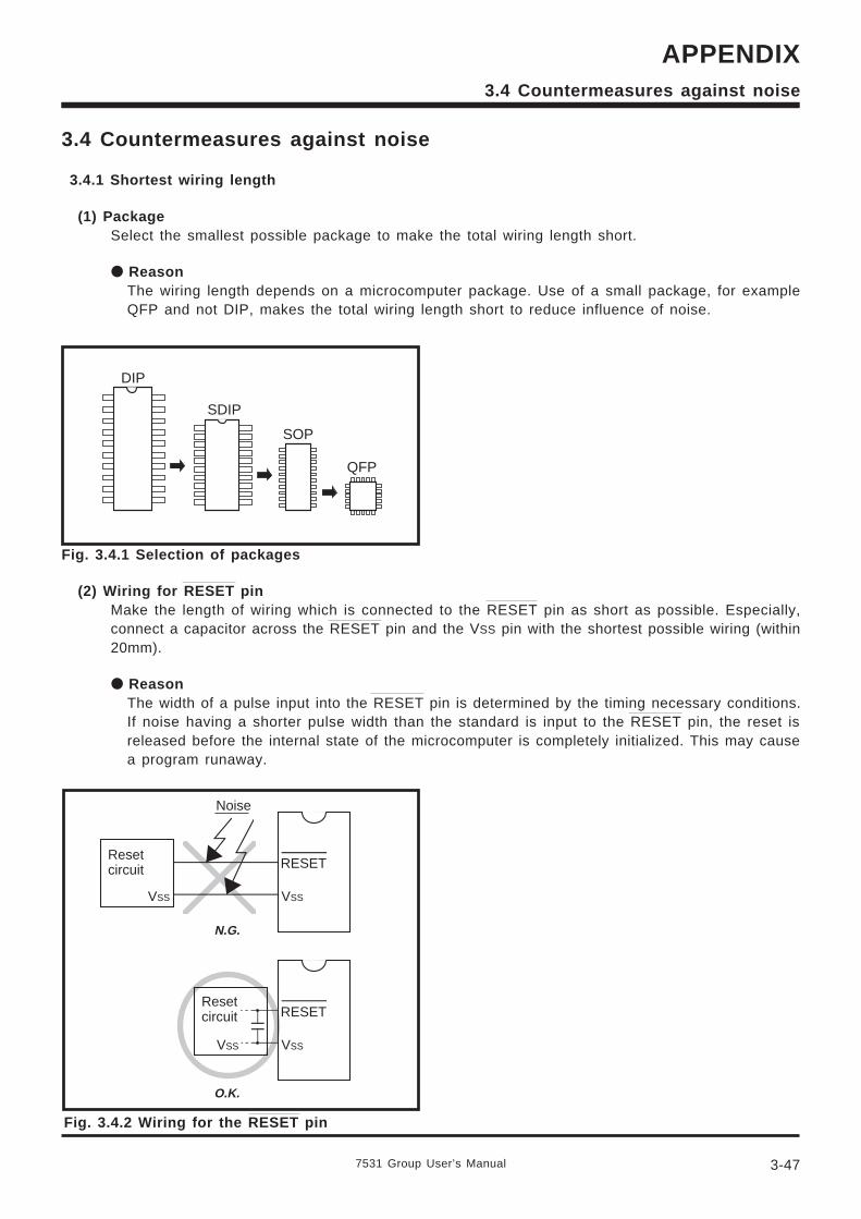
7531 Group User’s Manual 3-47
APPENDIX
Fig. 3.4.2 Wiring for the RESET pin
3.4 Countermeasures against noise
3.4 Countermeasures against noise
3.4.1 Shortest wiring length
(1) PackageSelect the smallest possible package to make the total wiring length short.
ReasonThe wiring length depends on a microcomputer package. Use of a small package, for exampleQFP and not DIP, makes the total wiring length short to reduce influence of noise.
Fig. 3.4.1 Selection of packages
(2) Wiring for RESET pinMake the length of wiring which is connected to the RESET pin as short as possible. Especially,connect a capacitor across the RESET pin and the VSS pin with the shortest possible wiring (within20mm).
ReasonThe width of a pulse input into the RESET pin is determined by the timing necessary conditions.If noise having a shorter pulse width than the standard is input to the RESET pin, the reset isreleased before the internal state of the microcomputer is completely initialized. This may causea program runaway.
DIP
SDIP
SOP
QFP
RESETReset circuit
Noise
VSSVSS
Reset circuit
VSS
RESET
VSS
N.G.
O.K.
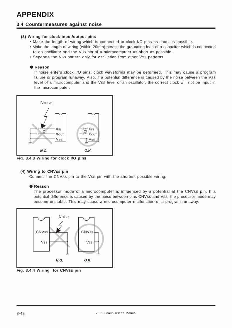
3-48
APPENDIX
7531 Group User’s Manual
(3) Wiring for clock input/output pins• Make the length of wiring which is connected to clock I/O pins as short as possible.• Make the length of wiring (within 20mm) across the grounding lead of a capacitor which is connected
to an oscillator and the VSS pin of a microcomputer as short as possible.• Separate the VSS pattern only for oscillation from other VSS patterns.
ReasonIf noise enters clock I/O pins, clock waveforms may be deformed. This may cause a programfailure or program runaway. Also, if a potential difference is caused by the noise between the VSS
level of a microcomputer and the VSS level of an oscillator, the correct clock will not be input inthe microcomputer.
Fig. 3.4.3 Wiring for clock I/O pins
(4) Wiring to CNV SS pinConnect the CNVSS pin to the VSS pin with the shortest possible wiring.
ReasonThe processor mode of a microcomputer is influenced by a potential at the CNVSS pin. If apotential difference is caused by the noise between pins CNVSS and VSS, the processor mode maybecome unstable. This may cause a microcomputer malfunction or a program runaway.
Fig. 3.4.4 Wiring for CNV SS pin
3.4 Countermeasures against noise
Noise
XIN
XOUT
VSS
XIN
XOUT
VSS
N.G. O.K.
Noise
CNVSS
VSS
CNVSS
VSS
N.G. O.K.
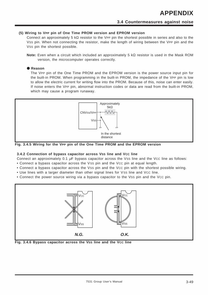
7531 Group User’s Manual 3-49
APPENDIX
(5) Wiring to V PP pin of One Time PROM version and EPROM versionConnect an approximately 5 kΩ resistor to the VPP pin the shortest possible in series and also to theVSS pin. When not connecting the resistor, make the length of wiring between the VPP pin and theVSS pin the shortest possible.
Note: Even when a circuit which included an approximately 5 kΩ resistor is used in the Mask ROMversion, the microcomputer operates correctly.
ReasonThe VPP pin of the One Time PROM and the EPROM version is the power source input pin forthe built-in PROM. When programming in the built-in PROM, the impedance of the VPP pin is lowto allow the electric current for writing flow into the PROM. Because of this, noise can enter easily.If noise enters the VPP pin, abnormal instruction codes or data are read from the built-in PROM,which may cause a program runaway.
Fig. 3.4.5 Wiring for the V PP pin of the One Time PROM and the EPROM version
3.4.2 Connection of bypass capacitor across V SS line and V CC lineConnect an approximately 0.1 µF bypass capacitor across the VSS line and the VCC line as follows:• Connect a bypass capacitor across the VSS pin and the VCC pin at equal length.• Connect a bypass capacitor across the VSS pin and the VCC pin with the shortest possible wiring.• Use lines with a larger diameter than other signal lines for VSS line and VCC line.• Connect the power source wiring via a bypass capacitor to the VSS pin and the VCC pin.
Fig. 3.4.6 Bypass capacitor across the V SS line and the V CC line
3.4 Countermeasures against noise
CNVSS/VPP
VSS
In the shortest distance
Approximately5kΩ
VSS
VCC
AAAAAAAAAAAA
VSS
VCC
AAAAAAAA
AAAAAA
AAAAAA
N.G. O.K.
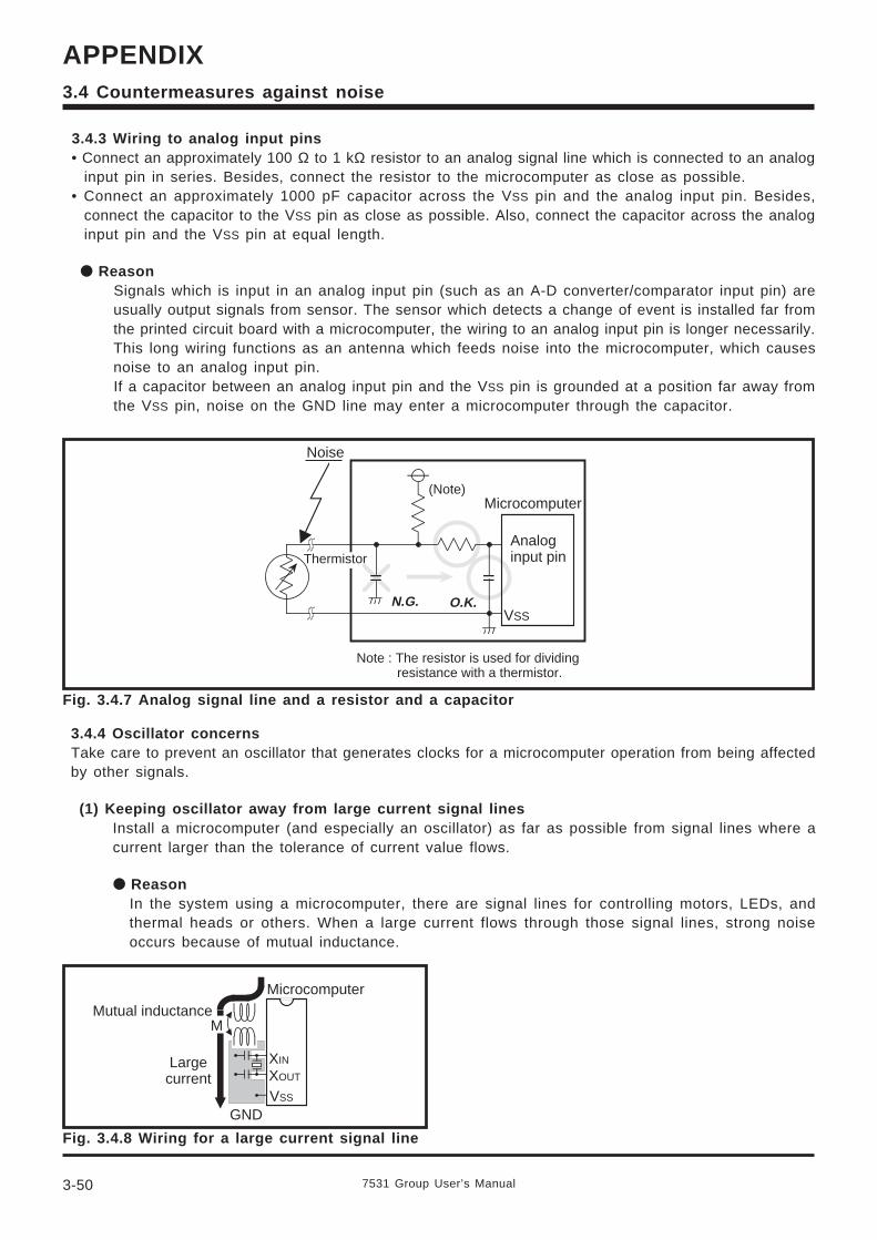
3-50
APPENDIX
7531 Group User’s Manual
3.4.3 Wiring to analog input pins• Connect an approximately 100 Ω to 1 kΩ resistor to an analog signal line which is connected to an analog
input pin in series. Besides, connect the resistor to the microcomputer as close as possible.• Connect an approximately 1000 pF capacitor across the VSS pin and the analog input pin. Besides,
connect the capacitor to the VSS pin as close as possible. Also, connect the capacitor across the analoginput pin and the VSS pin at equal length.
ReasonSignals which is input in an analog input pin (such as an A-D converter/comparator input pin) areusually output signals from sensor. The sensor which detects a change of event is installed far fromthe printed circuit board with a microcomputer, the wiring to an analog input pin is longer necessarily.This long wiring functions as an antenna which feeds noise into the microcomputer, which causesnoise to an analog input pin.If a capacitor between an analog input pin and the VSS pin is grounded at a position far away fromthe VSS pin, noise on the GND line may enter a microcomputer through the capacitor.
Fig. 3.4.7 Analog signal line and a resistor and a capacitor
3.4.4 Oscillator concernsTake care to prevent an oscillator that generates clocks for a microcomputer operation from being affectedby other signals.
(1) Keeping oscillator away from large current signal linesInstall a microcomputer (and especially an oscillator) as far as possible from signal lines where acurrent larger than the tolerance of current value flows.
ReasonIn the system using a microcomputer, there are signal lines for controlling motors, LEDs, andthermal heads or others. When a large current flows through those signal lines, strong noiseoccurs because of mutual inductance.
Fig. 3.4.8 Wiring for a large current signal line
3.4 Countermeasures against noise
Analog input pin
VSS
Noise
Thermistor
Microcomputer
N.G. O.K.
(Note)
Note : The resistor is used for dividing resistance with a thermistor.
XIN
XOUT
VSS
M
Microcomputer
Mutual inductance
Large current
GND
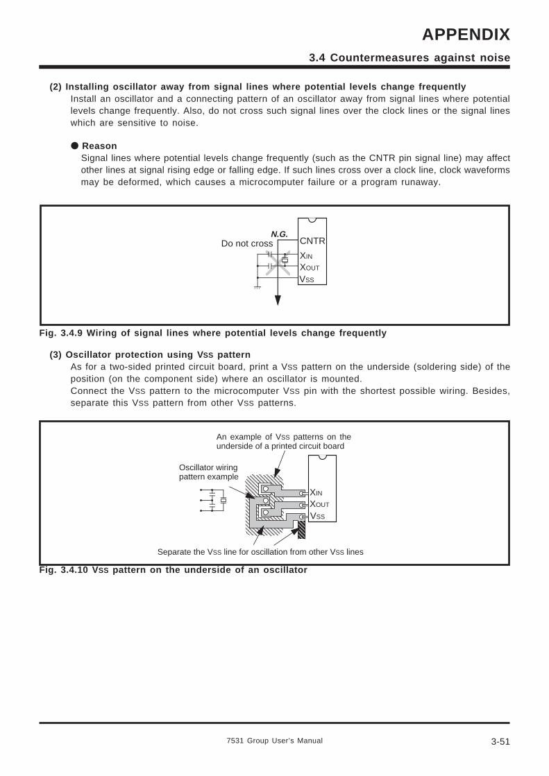
7531 Group User’s Manual 3-51
APPENDIX
(2) Installing oscillator away from signal lines where potential levels change frequentlyInstall an oscillator and a connecting pattern of an oscillator away from signal lines where potentiallevels change frequently. Also, do not cross such signal lines over the clock lines or the signal lineswhich are sensitive to noise.
ReasonSignal lines where potential levels change frequently (such as the CNTR pin signal line) may affectother lines at signal rising edge or falling edge. If such lines cross over a clock line, clock waveformsmay be deformed, which causes a microcomputer failure or a program runaway.
Fig. 3.4.9 Wiring of signal lines where potential levels change frequently
(3) Oscillator protection using V SS patternAs for a two-sided printed circuit board, print a VSS pattern on the underside (soldering side) of theposition (on the component side) where an oscillator is mounted.Connect the VSS pattern to the microcomputer VSS pin with the shortest possible wiring. Besides,separate this VSS pattern from other VSS patterns.
Fig. 3.4.10 V SS pattern on the underside of an oscillator
3.4 Countermeasures against noise
XIN
XOUT
VSS
CNTRDo not crossN.G.
AAAAAAAAA
AAAAAAAAAA
AAA
AAAAA
XIN
XOUT
VSS
An example of VSS patterns on the underside of a printed circuit board
Oscillator wiring pattern example
Separate the VSS line for oscillation from other VSS lines
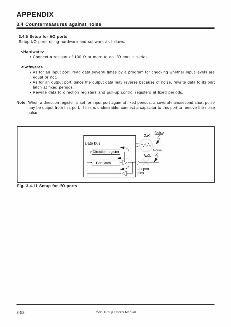
3-52
APPENDIX
7531 Group User’s Manual
Fig. 3.4.11 Setup for I/O ports
3.4.5 Setup for I/O portsSetup I/O ports using hardware and software as follows:
<Hardware>• Connect a resistor of 100 Ω or more to an I/O port in series.
<Software>• As for an input port, read data several times by a program for checking whether input levels are
equal or not.• As for an output port, since the output data may reverse because of noise, rewrite data to its port
latch at fixed periods.• Rewrite data to direction registers and pull-up control registers at fixed periods.
Note: When a direction register is set for input port again at fixed periods, a several-nanosecond short pulsemay be output from this port. If this is undesirable, connect a capacitor to this port to remove the noisepulse.
3.4 Countermeasures against noise
Direction register
Port latch
Data bus
I/O port pins
Noise
Noise
N.G.
O.K.
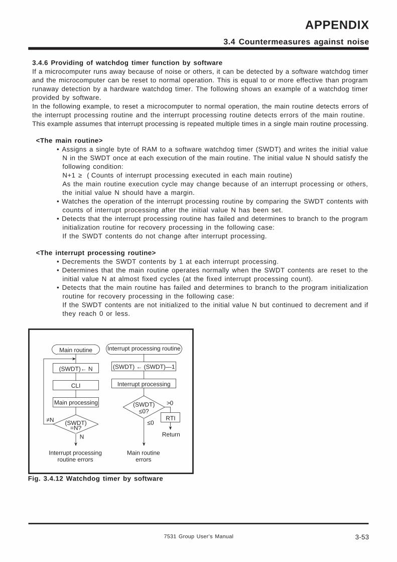
7531 Group User’s Manual 3-53
APPENDIX
3.4.6 Providing of watchdog timer function by softwareIf a microcomputer runs away because of noise or others, it can be detected by a software watchdog timerand the microcomputer can be reset to normal operation. This is equal to or more effective than programrunaway detection by a hardware watchdog timer. The following shows an example of a watchdog timerprovided by software.In the following example, to reset a microcomputer to normal operation, the main routine detects errors ofthe interrupt processing routine and the interrupt processing routine detects errors of the main routine.This example assumes that interrupt processing is repeated multiple times in a single main routine processing.
<The main routine>• Assigns a single byte of RAM to a software watchdog timer (SWDT) and writes the initial value
N in the SWDT once at each execution of the main routine. The initial value N should satisfy thefollowing condition:N+1 ≥ ( Counts of interrupt processing executed in each main routine)As the main routine execution cycle may change because of an interrupt processing or others,the initial value N should have a margin.
• Watches the operation of the interrupt processing routine by comparing the SWDT contents withcounts of interrupt processing after the initial value N has been set.
• Detects that the interrupt processing routine has failed and determines to branch to the programinitialization routine for recovery processing in the following case:If the SWDT contents do not change after interrupt processing.
<The interrupt processing routine>• Decrements the SWDT contents by 1 at each interrupt processing.• Determines that the main routine operates normally when the SWDT contents are reset to the
initial value N at almost fixed cycles (at the fixed interrupt processing count).• Detects that the main routine has failed and determines to branch to the program initialization
routine for recovery processing in the following case:If the SWDT contents are not initialized to the initial value N but continued to decrement and ifthey reach 0 or less.
Fig. 3.4.12 Watchdog timer by software
3.4 Countermeasures against noise
Main routine
(SWDT)← N
CLI
Main processing
(SWDT)
Interrupt processing routine errors
N
Interrupt processing routine
(SWDT) ← (SWDT)—1
Interrupt processing
(SWDT)
Main routine errors
>0
≤0RTI
Return=N?
≤0?≠N
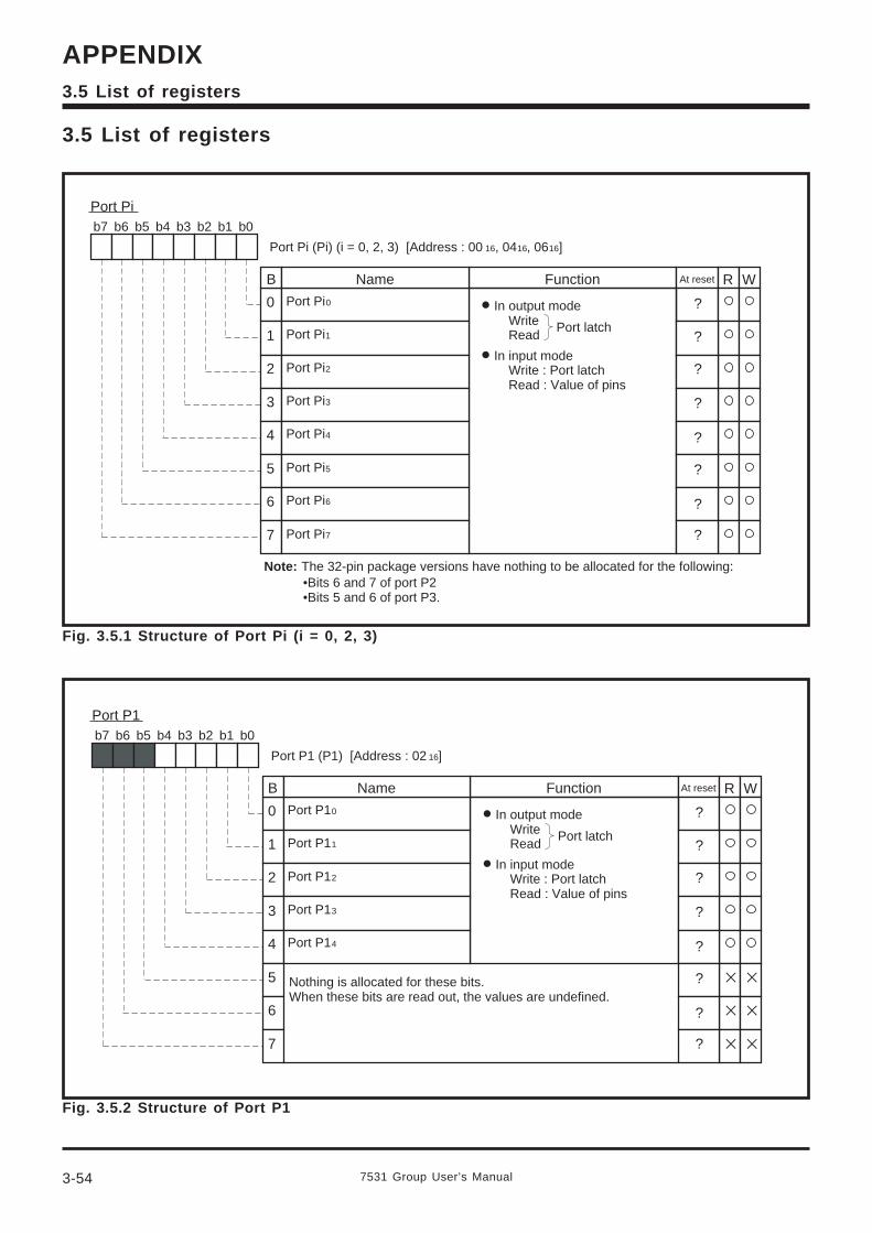
7531 Group User’s Manual3-54
APPENDIX3.5 List of registers
3.5 List of registers
Fig. 3.5.1 Structure of Port Pi (i = 0, 2, 3)
Port Pib7 b6 b5 b4 b3 b2 b1 b0
B Function At reset R W
0
1
2
3
4
5
6
7
Name
Port Pi0
Port Pi1
Port Pi2
Port Pi3
Port Pi4
Port Pi5
Port Pi6
Port Pi7
In output mode Write Read
Port latch
In input mode Write : Port latch Read : Value of pins
Port Pi (Pi) (i = 0, 2, 3) [Address : 00 16, 0416, 0616]
?
?
?
?
?
?
?
?
Note: The 32-pin package versions have nothing to be allocated for the following:•Bits 6 and 7 of port P2•Bits 5 and 6 of port P3.
Port P1b7 b6 b5 b4 b3 b2 b1 b0
B Function At reset R W
0
1
2
3
4
5
6
7
Name
Port P10
Port P11
Port P12
Port P13
Port P14
In output mode Write Read
Port latch
In input mode Write : Port latch Read : Value of pins
Port P1 (P1) [Address : 02 16]
?
?
?
?
?
?
?
?
Nothing is allocated for these bits.When these bits are read out, the values are undefined.
Fig. 3.5.2 Structure of Port P1
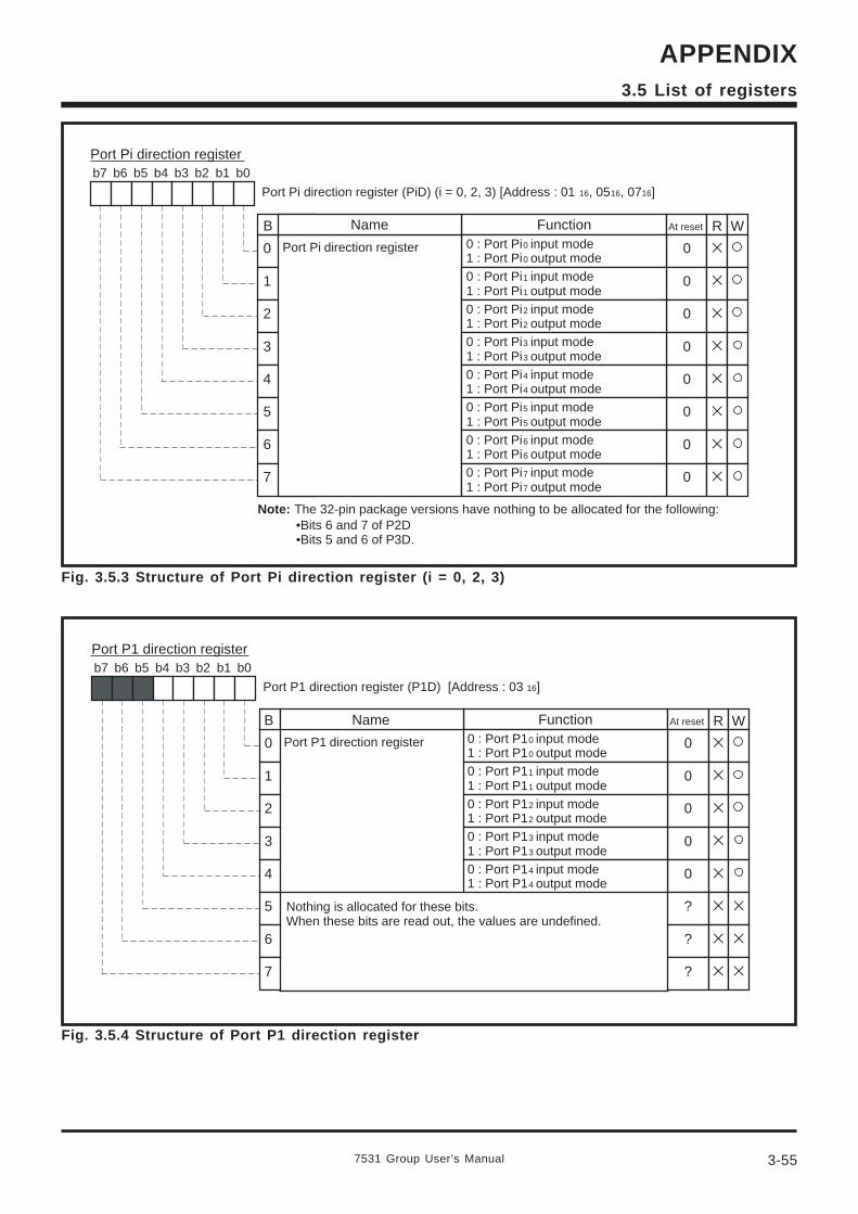
7531 Group User’s Manual 3-55
APPENDIX3.5 List of registers
Fig. 3.5.3 Structure of Port Pi direction register (i = 0, 2, 3)
Fig. 3.5.4 Structure of Port P1 direction register
Port Pi direction registerb7 b6 b5 b4 b3 b2 b1 b0
B Function At reset R W
0
1
2
3
4
5
6
7
Name
Port Pi direction register 0
0
0
0
0
0
0
0
Port Pi direction register (PiD) (i = 0, 2, 3) [Address : 01 16, 0516, 0716]
0 : Port Pi0 input mode1 : Port Pi0 output mode0 : Port Pi1 input mode1 : Port Pi1 output mode0 : Port Pi2 input mode1 : Port Pi2 output mode0 : Port Pi3 input mode1 : Port Pi3 output mode0 : Port Pi4 input mode1 : Port Pi4 output mode0 : Port Pi5 input mode1 : Port Pi5 output mode0 : Port Pi6 input mode1 : Port Pi6 output mode0 : Port Pi7 input mode1 : Port Pi7 output mode
Note: The 32-pin package versions have nothing to be allocated for the following:•Bits 6 and 7 of P2D•Bits 5 and 6 of P3D.
Port P1 direction registerb7 b6 b5 b4 b3 b2 b1 b0
B Function At reset R W
0
1
2
3
4
5
6
7
Name
Port P1 direction register 0
0
0
0
0
?
?
?
Port P1 direction register (P1D) [Address : 03 16]
0 : Port P10 input mode1 : Port P10 output mode0 : Port P11 input mode1 : Port P11 output mode0 : Port P12 input mode1 : Port P12 output mode0 : Port P13 input mode1 : Port P13 output mode0 : Port P14 input mode1 : Port P14 output mode
Nothing is allocated for these bits.When these bits are read out, the values are undefined.
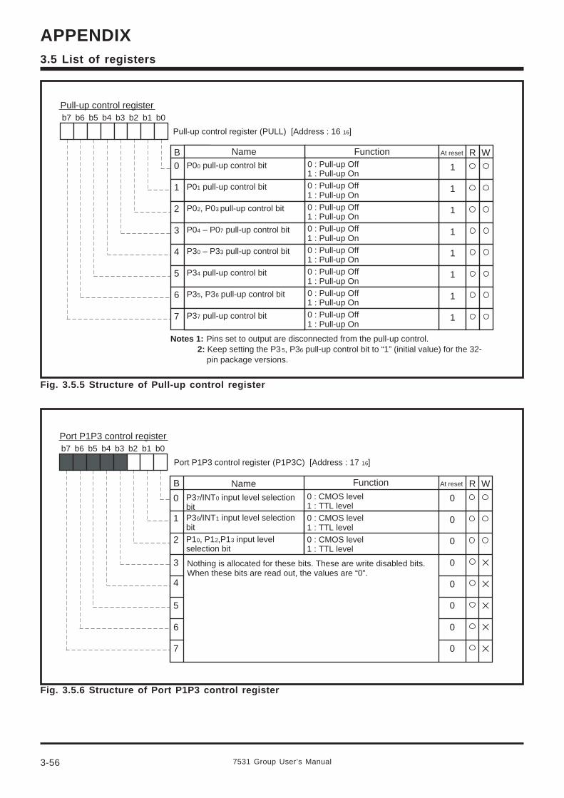
7531 Group User’s Manual3-56
APPENDIX3.5 List of registers
Fig. 3.5.5 Structure of Pull-up control register
Pull-up control registerb7 b6 b5 b4 b3 b2 b1 b0
B Function At reset R W0
1
2
3
4
5
6
7
NameP00 pull-up control bit 1
1
1
1
1
1
1
1
Pull-up control register (PULL) [Address : 16 16]
0 : Pull-up Off1 : Pull-up On
Notes 1: Pins set to output are disconnected from the pull-up control.2: Keep setting the P3 5, P36 pull-up control bit to “1” (initial value) for the 32-
pin package versions.
P01 pull-up control bit 0 : Pull-up Off1 : Pull-up On
P02, P03 pull-up control bit 0 : Pull-up Off1 : Pull-up On
P04 – P07 pull-up control bit 0 : Pull-up Off1 : Pull-up On
P30 – P33 pull-up control bit 0 : Pull-up Off1 : Pull-up On
P34 pull-up control bit 0 : Pull-up Off1 : Pull-up On
P35, P36 pull-up control bit 0 : Pull-up Off1 : Pull-up On
P37 pull-up control bit 0 : Pull-up Off1 : Pull-up On
Fig. 3.5.6 Structure of Port P1P3 control register
Port P1P3 control registerb7 b6 b5 b4 b3 b2 b1 b0
B Function At reset R W
0
1
2
3
4
5
6
7
NameP37/INT0 input level selection bit
0
0
0
0
0
0
0
0
Port P1P3 control register (P1P3C) [Address : 17 16]
0 : CMOS level1 : TTL level
P36/INT1 input level selection bit
0 : CMOS level1 : TTL level
P10, P12,P13 input level selection bit
0 : CMOS level1 : TTL level
Nothing is allocated for these bits. These are write disabled bits.When these bits are read out, the values are “0”.
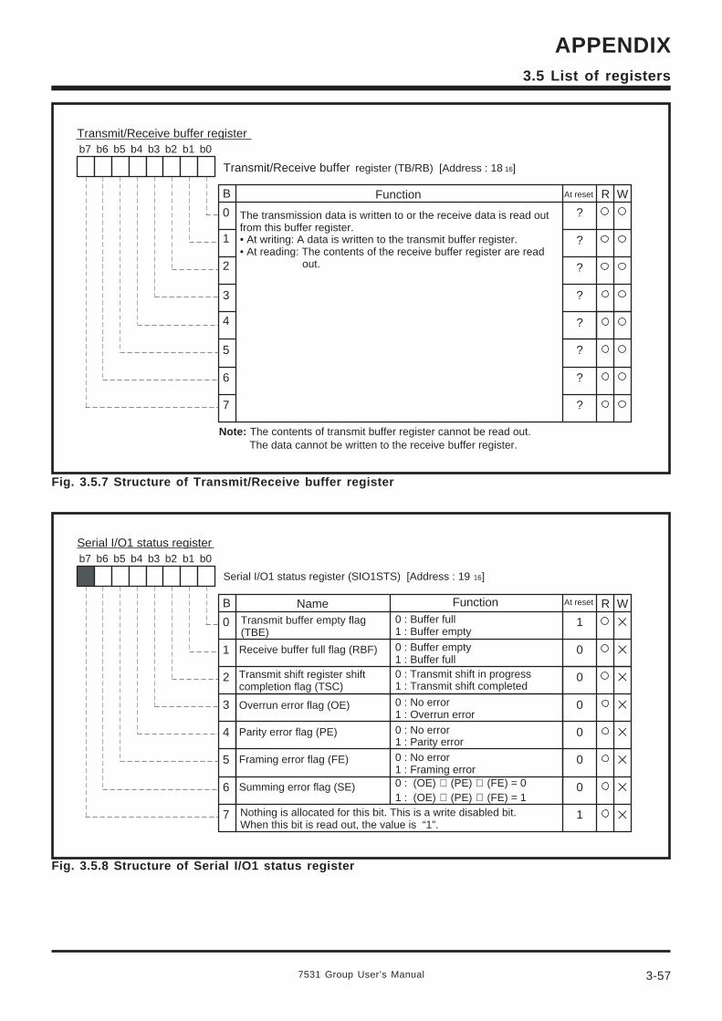
7531 Group User’s Manual 3-57
APPENDIX3.5 List of registers
Fig. 3.5.7 Structure of Transmit/Receive buffer register
Transmit/Receive buffer registerb7 b6 b5 b4 b3 b2 b1 b0
B Function At reset R W
0
1
2
3
4
5
6
7
?
?
?
?
?
?
?
?
Transmit/Receive buffer register (TB/RB) [Address : 18 16]
The transmission data is written to or the receive data is read out from this buffer register.• At writing: A data is written to the transmit buffer register.• At reading: The contents of the receive buffer register are read
out.
Note: The contents of transmit buffer register cannot be read out.The data cannot be written to the receive buffer register.
Serial I/O1 status registerb7 b6 b5 b4 b3 b2 b1 b0
B Function At reset R W
0
1
2
3
4
5
6
7
Name
1
0
0
0
0
0
0
1
Serial I/O1 status register (SIO1STS) [Address : 19 16]
Nothing is allocated for this bit. This is a write disabled bit.When this bit is read out, the value is “1”.
Transmit buffer empty flag (TBE)
0 : (OE) ∪ (PE) ∪ (FE) = 01 : (OE) ∪ (PE) ∪ (FE) = 1
Overrun error flag (OE)
0 : Buffer full1 : Buffer empty
Receive buffer full flag (RBF)
Transmit shift register shift completion flag (TSC)
Parity error flag (PE)
Framing error flag (FE)
Summing error flag (SE)
0 : Buffer empty1 : Buffer full0 : Transmit shift in progress1 : Transmit shift completed
0 : No error1 : Overrun error0 : No error1 : Parity error0 : No error1 : Framing error
Fig. 3.5.8 Structure of Serial I/O1 status register
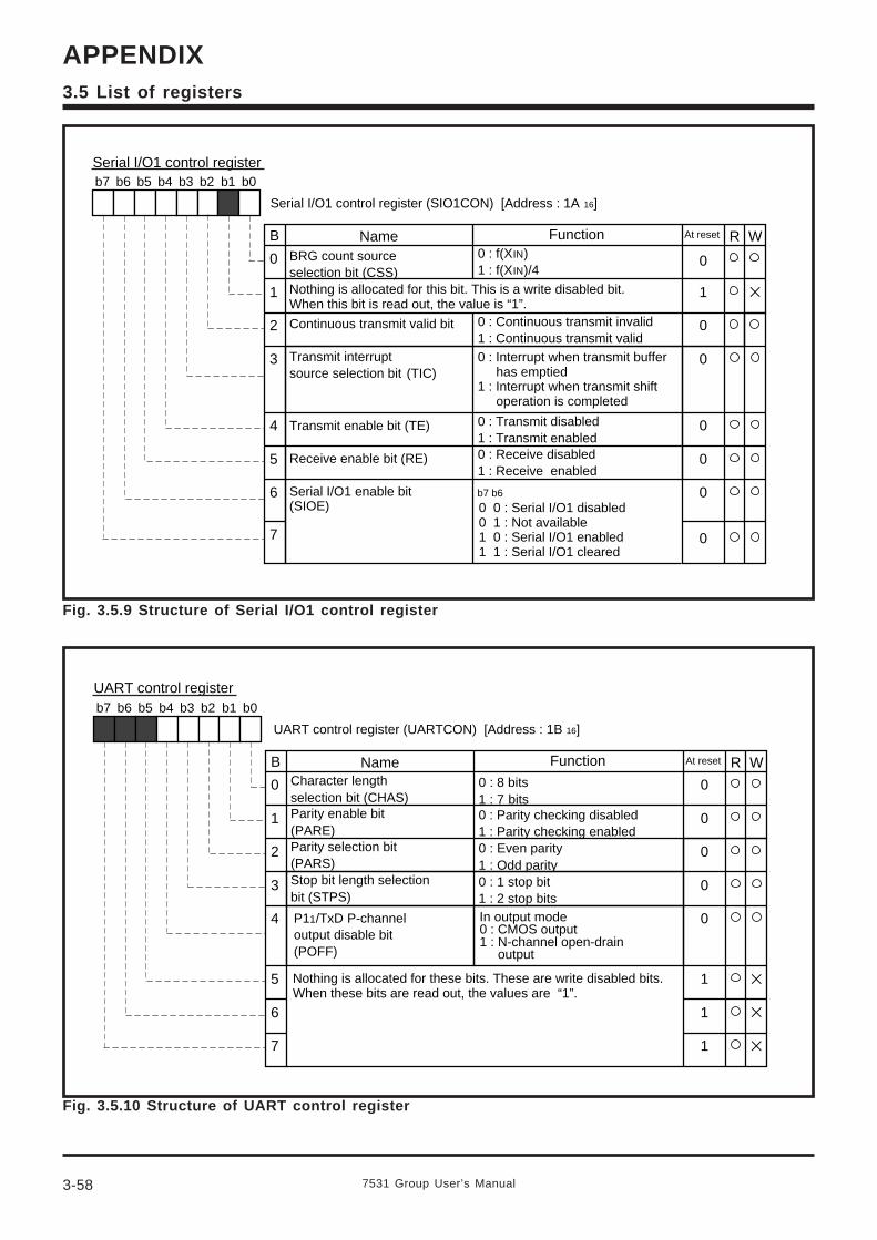
7531 Group User’s Manual3-58
APPENDIX3.5 List of registers
Fig. 3.5.9 Structure of Serial I/O1 control register
Serial I/O1 control registerb7 b6 b5 b4 b3 b2 b1 b0
B Function At reset R W
0
1
2
3
4
5
6
7
Name
1
0
0
0
0
0
0
Serial I/O1 control register (SIO1CON) [Address : 1A 16]
Nothing is allocated for this bit. This is a write disabled bit.When this bit is read out, the value is “1”.
0 : f(XIN)1 : f(XIN)/4
BRG count source selection bit (CSS)
0
0 : Transmit disabled1 : Transmit enabled0 : Receive disabled1 : Receive enabled
Transmit interrupt source selection bit (TIC)
Transmit enable bit (TE)
Receive enable bit (RE)
Serial I/O1 enable bit(SIOE)
Continuous transmit valid bit 0 : Continuous transmit invalid1 : Continuous transmit valid0 : Interrupt when transmit buffer
has emptied1 : Interrupt when transmit shift
operation is completed
0 0 : Serial I/O1 disabled0 1 : Not available1 0 : Serial I/O1 enabled1 1 : Serial I/O1 cleared
b7 b6
b7 b6 b5 b4 b3 b2 b1 b0
B Function At reset R W
0
1
2
3
4
5
6
7
Name
0
0
0
0
1
UART control register (UARTCON) [Address : 1B 16]
Nothing is allocated for these bits. These are write disabled bits.When these bits are read out, the values are “1”.
UART control register
Character length selection bit (CHAS)Parity enable bit(PARE)
Stop bit length selectionbit (STPS)
Parity selection bit(PARS)
In output mode0 : CMOS output1 : N-channel open-drain output
0 : 8 bits1 : 7 bits0 : Parity checking disabled1 : Parity checking enabled
0 : 1 stop bit1 : 2 stop bits
0 : Even parity1 : Odd parity
P11/TxD P-channel output disable bit(POFF)
1
1
0
Fig. 3.5.10 Structure of UART control register
7531 Group User’s Manual 3-59
APPENDIX3.5 List of registers
Fig. 3.5.11 Structure of Baud rate generator
Baud rate generatorb7 b6 b5 b4 b3 b2 b1 b0
B Function At reset R W
0
1
2
3
4
5
6
7
?
?
?
?
?
?
?
?
Baud rate generator (BRG) [Address : 1C 16]
Set a count value of baud rate generator.
Prescaler 12, Prescaler Xb7 b6 b5 b4 b3 b2 b1 b0
B Function At reset R W
0
1
2
3
4
5
6
7
1
1
1
1
1
1
1
1
Prescaler 12 (PRE12) [Address : 28 16]Prescaler X (PREX) [Address : 2C 16]
•Set a count value of each prescaler.•The value set in this register is written to both each prescaler and the corresponding prescaler latch at the same time.•When this register is read out, the count value of the corres-ponding prescaler is read out.
Fig. 3.5.12 Structure of Prescaler 12, Prescaler X
7531 Group User’s Manual3-60
APPENDIX3.5 List of registers
Fig. 3.5.13 Structure of Timer 1
Timer 1b7 b6 b5 b4 b3 b2 b1 b0
B Function At reset R W
0
1
2
3
4
5
6
7
1
0
0
0
0
0
0
0
Timer 1 (T1) [Address : 29 16]
•Set a count value of timer 1.•The value set in this register is written to both timer 1 and timer 1
latch at the same time.•When this register is read out, the timer 1’s count value is read
out.
Timer 2b7 b6 b5 b4 b3 b2 b1 b0
B Function At reset R W
0
1
2
3
4
5
6
7
0
0
0
0
0
0
0
0
Timer 2 (T2) [Address : 2A 16]
•Set a count value of timer 2.•The value set in this register is written to both timer 2 and timer 2
latch at the same time.•When this register is read out, the timer 2’s count value is read
out.
Fig. 3.5.14 Structure of Timer 2
7531 Group User’s Manual 3-61
APPENDIX3.5 List of registers
Fig. 3.5.15 Structure of Timer X mode register
b7 b6 b5 b4 b3 b2 b1 b0
B Function At reset R W
0
2
3
4
5
6
7
Name
0
0
0
0
Timer X mode register (TM) [Address : 2B 16]
Nothing is allocated for these bits. These are write disabled bits.When these bits are read out, the values are “0”.
Timer X mode register
0
0
00 0 : Timer mode0 1 : Pulse output mode1 0 : Event counter mode1 1 : Pulse width measurement
mode
b1 b0
1 0
Timer X operating mode bits
CNTR0 active edge switch bit The function depends on the operating mode.(Refer to Table 3.5.1)
Timer X count stop bit 0 : Count start1 : Count stop
Timer X operation modes
Timer mode
Pulse output mode
Event counter mode
Pulse width measurement mode
CNTR0 active edge switch bit (bit 2 of address 2B16) contents
“0” CNTR0 interrupt request occurrence: Falling edge
; No influence to timer count
“1” CNTR0 interrupt request occurrence: Rising edge
; No influence to timer count
“0” Pulse output start: Beginning at “H” level
CNTR0 interrupt request occurrence: Falling edge
“1” Pulse output start: Beginning at “L” level
CNTR0 interrupt request occurrence: Rising edge
“0” Timer X: Rising edge count
CNTR0 interrupt request occurrence: Falling edge
“1” Timer X: Falling edge count
CNTR0 interrupt request occurrence: Rising edge
“0” Timer X: “H” level width measurement
CNTR0 interrupt request occurrence: Falling edge
“1” Timer X: “L” level width measurement
CNTR0 interrupt request occurrence: Rising edge
Table 3.5.1 CNTR0 active edge switch bit function
7531 Group User’s Manual3-62
APPENDIX3.5 List of registers
Fig. 3.5.16 Structure of Timer X
Timer Xb7 b6 b5 b4 b3 b2 b1 b0
B Function At reset R W
0
1
2
3
4
5
6
7
1
1
1
1
1
1
1
1
Timer X (TX) [Address : 2D 16]
•Set a count value of timer X.•The value set in this register is written to both timer X and timer X
latch at the same time.•When this register is read out, the timer X’s count value is read
out.
b7 b6 b5 b4 b3 b2 b1 b0
B Function At reset R W
0
1
2
3
4
5
6
7
Name
0
0
0
0
0
Timer count source set register (TCSS) [Address : 2E 16]
Nothing is allocated for these bits. These are write disabled bits.When these bits are read out, the values are “0”.
Timer count source set register
Timer X count source selection bit (Note)
0 : f(XIN) / 161 : f(XIN) / 2
0
0
0
Note: To switch the timer X count source selection bit, stop the timer X count operation before do that.
Fig. 3.5.17 Structure of Timer count source set register
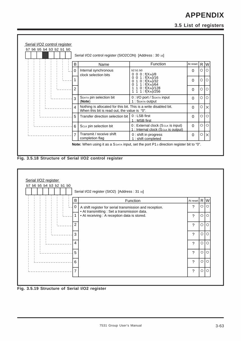
7531 Group User’s Manual 3-63
APPENDIX3.5 List of registers
Fig. 3.5.18 Structure of Serial I/O2 control register
Serial I/O2 registerb7 b6 b5 b4 b3 b2 b1 b0
B Function At reset R W
0
1
2
3
4
5
6
7
?
?
?
?
?
?
?
?
Serial I/O2 register (SIO2) [Address : 31 16]
A shift register for serial transmission and reception.• At transmitting : Set a transmission data.• At receiving : A reception data is stored.
b7 b6 b5 b4 b3 b2 b1 b0
B Function At reset R W
0
1
2
3
4
5
6
7
Name
0
0
0
0
Serial I/O2 control register (SIO2CON) [Address : 30 16]
Nothing is allocated for this bit. This is a write disabled bit.When this bit is read out, the value is “0”.
Serial I/O2 control register
0
0
Note: When using it as a S DATA input, set the port P13 direction register bit to “0”.
0 : LSB first1 : MSB first
0 0 0 : f(XIN)/80 0 1 : f(XIN)/160 1 0 : f(XIN)/320 1 1 : f(XIN)/641 1 0 : f(XIN)/1281 1 1 : f(XIN)/256
Internal synchronous clock selection bits
Transfer direction selection bit
b2 b1 b0
SDATA pin selection bit(Note)
0 : I/O port / SDATA input1 : SDATA output
SCLK pin selection bit 0 : External clock (SCLK is input)1 : Internal clock (SCLK is output)
Transmit / receive shift completion flag
0 : shift in progress1 : shift completed
0
0
Fig. 3.5.19 Structure of Serial I/O2 register
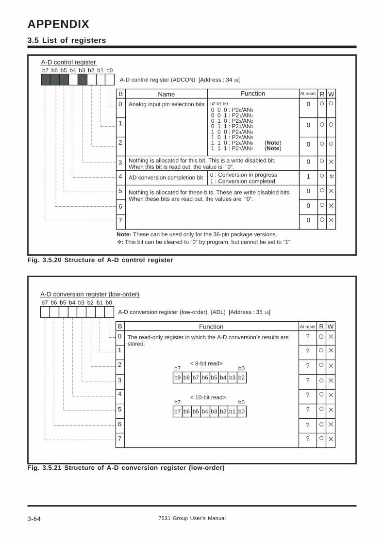
7531 Group User’s Manual3-64
APPENDIX3.5 List of registers
Fig. 3.5.20 Structure of A-D control register
A-D conversion register (low-order)b7 b6 b5 b4 b3 b2 b1 b0
B Function At reset R W
0
1
2
3
4
5
6
7
?
?
?
?
?
?
?
?
A-D conversion register (low-order) (ADL) [Address : 35 16]
The read-only register in which the A-D conversion’s results are stored.
< 8-bit read>b7
b8 b7 b6 b5 b4 b3
b0
b2b9
< 10-bit read>b7
b6 b5 b4 b3 b2 b1
b0
b0b7
Fig. 3.5.21 Structure of A-D conversion register (low-order)
b7 b6 b5 b4 b3 b2 b1 b0
B Function At reset R W
0
1
2
3
4
5
6
7
Name
0
1
0
0
A-D control register (ADCON) [Address : 34 16]
Nothing is allocated for this bit. This is a write disabled bit.When this bit is read out, the value is “0”.
A-D control register
0
Note: These can be used only for the 36-pin package versions.
0 0 0 : P20/AN00 0 1 : P21/AN10 1 0 : P22/AN20 1 1 : P23/AN31 0 0 : P24/AN41 0 1 : P25/AN51 1 0 : P26/AN6 (Note)1 1 1 : P27/AN7 (Note)
Analog input pin selection bits b2 b1 b0
0
0
AD conversion completion bit 0 : Conversion in progress1 : Conversion completed
Nothing is allocated for these bits. These are write disabled bits.When these bits are read out, the values are “0”.
0
: This bit can be cleared to “0” by program, but cannot be set to “1”.
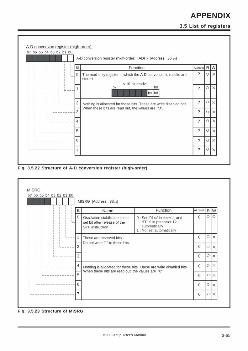
7531 Group User’s Manual 3-65
APPENDIX3.5 List of registers
Fig. 3.5.22 Structure of A-D conversion register (high-order)
A-D conversion register (high-order)b7 b6 b5 b4 b3 b2 b1 b0
B Function At reset R W
0
1
2
3
4
5
6
7
?
?
?
?
?
?
?
?
A-D conversion register (high-order) (ADH) [Address : 36 16]
The read-only register in which the A-D conversion’s results are stored.
< 10-bit read>b7
b9
b0
b8
Nothing is allocated for these bits. These are write disabled bits.When these bits are read out, the values are “0”.
b7 b6 b5 b4 b3 b2 b1 b0
B Function At reset R W
0
1
2
3
4
5
6
7
Name
0
0
0
0
MISRG [Address : 38 16]
Nothing is allocated for these bits. These are write disabled bits.When these bits are read out, the values are “0”.
MISRG
Oscillation stabilization time set bit after release of theSTP instruction
00 : Set “0116” in timer 1, and“FF16” in prescaler 12 automatically
1 : Not set automatically
These are reserved bits.Do not write “1” to these bits.
0
0
0
Fig. 3.5.23 Structure of MISRG
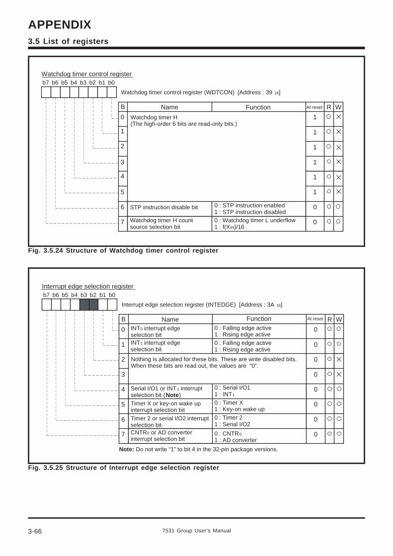
7531 Group User’s Manual3-66
APPENDIX3.5 List of registers
Fig. 3.5.24 Structure of Watchdog timer control register
Watchdog timer control registerb7 b6 b5 b4 b3 b2 b1 b0
B Function At reset R W
0
1
2
3
4
5
6
7
Name
1
1
1
1
1
1
0
0
Watchdog timer control register (WDTCON) [Address : 39 16]
Watchdog timer H(The high-order 6 bits are read-only bits.)
STP instruction disable bit 0 : STP instruction enabled1 : STP instruction disabled
Watchdog timer H count source selection bit
0 : Watchdog timer L underflow1 : f(XIN)/16
Fig. 3.5.25 Structure of Interrupt edge selection register
Interrupt edge selection registerb7 b6 b5 b4 b3 b2 b1 b0
B Function At reset R W
0
1
2
3
4
5
6
7
Name
0
0
0
0
0
0
0
0
Interrupt edge selection register (INTEDGE) [Address : 3A 16]
Nothing is allocated for these bits. These are write disabled bits.When these bits are read out, the values are “0”.
INT0 interrupt edge selection bitINT1 interrupt edge selection bit
0 : Falling edge active1 : Rising edge active0 : Falling edge active1 : Rising edge active
Serial I/O1 or INT1 interrupt selection bit (Note)Timer X or key-on wake up interrupt selection bitTimer 2 or serial I/O2 interrupt selection bitCNTR0 or AD converter interrupt selection bit
0 : Serial I/O11 : INT1
0 : Timer X1 : Key-on wake up0 : Timer 21 : Serial I/O2
0 : CNTR0
1 : AD converter
Note: Do not write “1” to bit 4 in the 32-pin package versions.
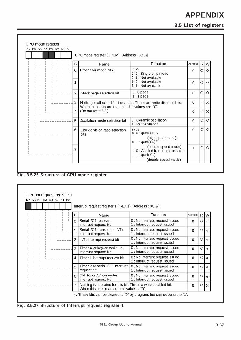
7531 Group User’s Manual 3-67
APPENDIX3.5 List of registers
Fig. 3.5.26 Structure of CPU mode register
Interrupt request register 1b7 b6 b5 b4 b3 b2 b1 b0
B Function At reset R W
0
1
2
3
4
5
6
7
Name
0
0
0
0
0
0
0
0
Interrupt request register 1 (IREQ1) [Address : 3C 16]
Nothing is allocated for this bit. This is a write disabled bit.When this bit is read out, the value is “0”.
Serial I/O1 receive interrupt request bitSerial I/O1 transmit or INT 1 interrupt request bit
0 : No interrupt request issued1 : Interrupt request issued
Timer 2 or serial I/O2 interrupt request bit
CNTR0 or AD converter interrupt request bit
: These bits can be cleared to “0” by program, but cannot be set to “1”.
0 : No interrupt request issued1 : Interrupt request issued
INT0 interrupt request bit
Timer X or key-on wake up interrupt request bit
0 : No interrupt request issued1 : Interrupt request issued0 : No interrupt request issued1 : Interrupt request issued
Timer 1 interrupt request bit 0 : No interrupt request issued1 : Interrupt request issued0 : No interrupt request issued1 : Interrupt request issued0 : No interrupt request issued1 : Interrupt request issued
Fig. 3.5.27 Structure of Interrupt request register 1
b7 b6 b5 b4 b3 b2 b1 b0
B Function At reset R W
0
2
3
4
5
6
7
Name
0
0
0
1
CPU mode register (CPUM) [Address : 3B 16]
Nothing is allocated for these bits. These are write disabled bits.When these bits are read out, the values are “0”.(Do not write “1”.)
CPU mode register
0
0
00 0 : Single-chip mode0 1 : Not available1 0 : Not available1 1 : Not available
b1 b0
1 0
Processor mode bits
0 : Ceramic oscillation1 : RC oscillation
0 : 0 page1 : 1 page
Stack page selection bit
Oscillation mode selection bit
Clock division ratio selection bits 0 0 : φ = f(XIN)/2
(high-speedmode)0 1 : φ = f(XIN)/8
(middle-speed mode)1 0 : Applied from ring oscillator1 1 : φ = f(XIN)
(double-speed mode)
b7 b6
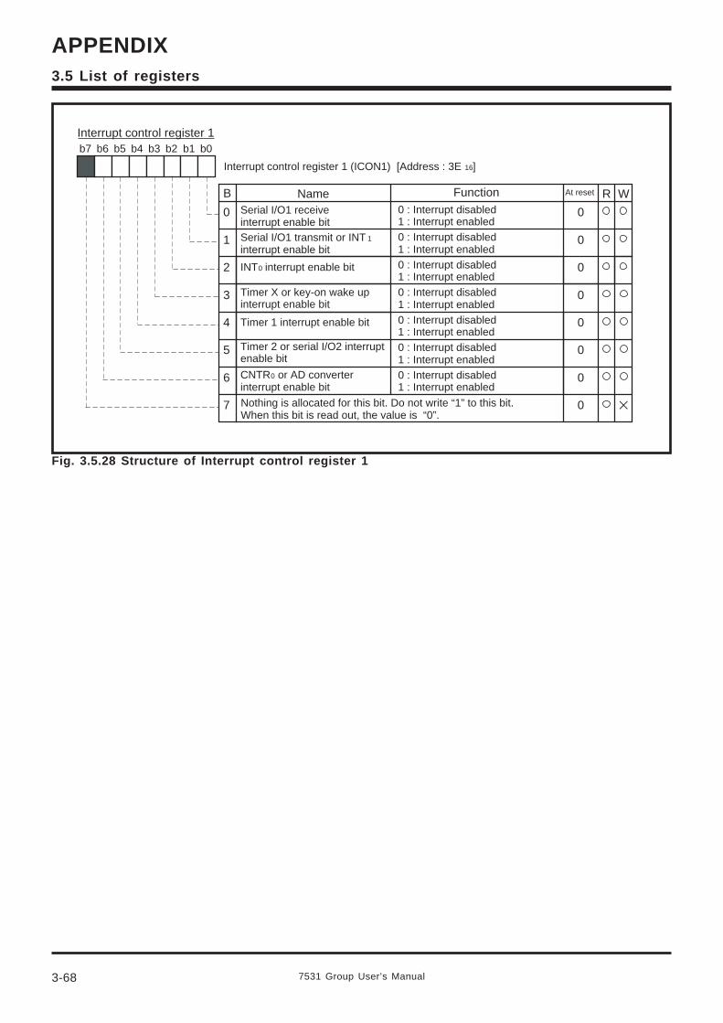
7531 Group User’s Manual3-68
APPENDIX3.5 List of registers
Interrupt control register 1b7 b6 b5 b4 b3 b2 b1 b0
B Function At reset R W
0
1
2
3
4
5
6
7
Name
0
0
0
0
0
0
0
0
Interrupt control register 1 (ICON1) [Address : 3E 16]
Nothing is allocated for this bit. Do not write “1” to this bit.When this bit is read out, the value is “0”.
Serial I/O1 receive interrupt enable bitSerial I/O1 transmit or INT 1 interrupt enable bit
0 : Interrupt disabled1 : Interrupt enabled
Timer 2 or serial I/O2 interrupt enable bit
CNTR0 or AD converter interrupt enable bit
INT0 interrupt enable bit
Timer X or key-on wake up interrupt enable bit
Timer 1 interrupt enable bit
0 : Interrupt disabled1 : Interrupt enabled0 : Interrupt disabled1 : Interrupt enabled0 : Interrupt disabled1 : Interrupt enabled0 : Interrupt disabled1 : Interrupt enabled0 : Interrupt disabled1 : Interrupt enabled0 : Interrupt disabled1 : Interrupt enabled
Fig. 3.5.28 Structure of Interrupt control register 1
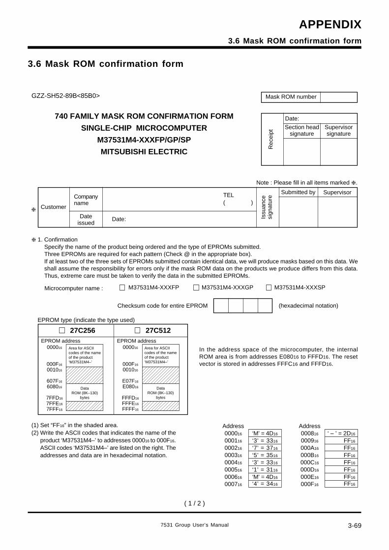
7531 Group User’s Manual 3-69
APPENDIX
GZZ-SH52-89B<85B0>
Checksum code for entire EPROM (hexadecimal notation)
(1) Set “FF16” in the shaded area.(2) Write the ASCII codes that indicates the name of the
product ‘M37531M4–’ to addresses 000016 to 000F16.ASCII codes ‘M37531M4–’ are listed on the right. Theaddresses and data are in hexadecimal notation.
Address000016
000116
000216
000316
000416
000516
000616
000716
‘M’ = 4D16
‘3’ = 3316
‘7’ = 3716
‘5’ = 3516
‘3’ = 3316
‘1’ = 3116
‘M’ = 4D16
‘4’ = 3416
Address000816
000916
000A16
000B16
000C16
000D16
000E16
000F16
‘ – ’ = 2D16
FF16
FF16
FF16
FF16
FF16
FF16
FF16
EPROM type (indicate the type used)
27C256 27C512
000016
000F16
001016
607F16
608016
7FFD16
7FFE16
7FFF16
EPROM addressArea for ASCIIcodes of the nameof the product‘M37531M4–’
Mask ROM number
1. ConfirmationSpecify the name of the product being ordered and the type of EPROMs submitted.Three EPROMs are required for each pattern (Check @ in the appropriate box).If at least two of the three sets of EPROMs submitted contain identical data, we will produce masks based on this data. Weshall assume the responsibility for errors only if the mask ROM data on the products we produce differs from this data.Thus, extreme care must be taken to verify the data in the submitted EPROMs.
Microcomputer name : M37531M4-XXXGPM37531M4-XXXFP M37531M4-XXXSP
DataROM (8K–130)
bytes
EPROM address 000016
000F16
001016
E07F16
E08016
FFFD16
FFFE16
FFFF16
Area for ASCIIcodes of the nameof the product‘M37531M4–’
DataROM (8K–130)
bytes
In the address space of the microcomputer, the internalROM area is from addresses E08016 to FFFD16. The resetvector is stored in addresses FFFC16 and FFFD16.
740 FAMILY MASK ROM CONFIRMATION FORM
SINGLE-CHIP MICROCOMPUTER
M37531M4-XXXFP/GP/SP
MITSUBISHI ELECTRIC
Rec
eipt
Date:
Section headsignature
Supervisorsignature
Companyname
Note : Please fill in all items marked .
Customer
Issu
ance
sign
atur
e
Dateissued
Submitted byTEL( )
Date:
Supervisor
3.6 Mask ROM confirmation form
( 1 / 2 )
3.6 Mask ROM confirmation form
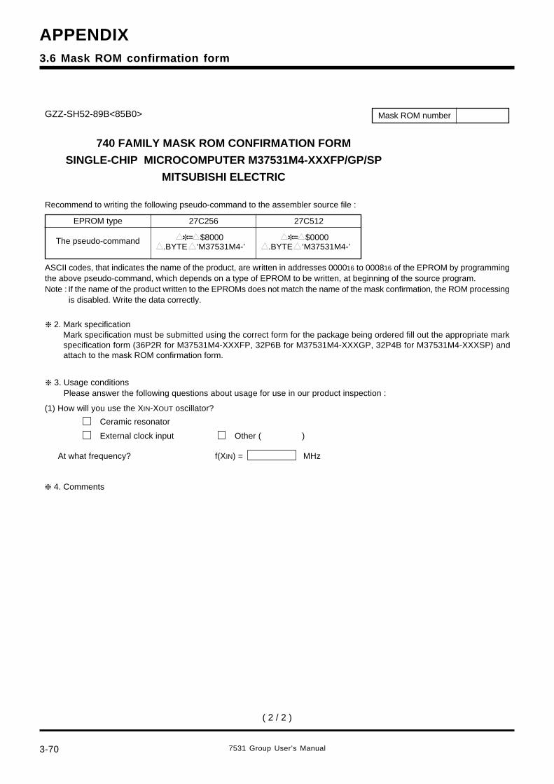
3-70
APPENDIX
7531 Group User’s Manual
= $8000 .BYTE ‘M37531M4-’
= $0000 .BYTE ‘M37531M4-’
740 FAMILY MASK ROM CONFIRMATION FORM
SINGLE-CHIP MICROCOMPUTER M37531M4-XXXFP/GP/SP
MITSUBISHI ELECTRIC
GZZ-SH52-89B<85B0>
Recommend to writing the following pseudo-command to the assembler source file :
27C256 27C512EPROM type
The pseudo-command
ASCII codes, that indicates the name of the product, are written in addresses 000016 to 000816 of the EPROM by programmingthe above pseudo-command, which depends on a type of EPROM to be written, at beginning of the source program.Note : If the name of the product written to the EPROMs does not match the name of the mask confirmation, the ROM processing
is disabled. Write the data correctly.
Mask ROM number
2. Mark specificationMark specification must be submitted using the correct form for the package being ordered fill out the appropriate markspecification form (36P2R for M37531M4-XXXFP, 32P6B for M37531M4-XXXGP, 32P4B for M37531M4-XXXSP) andattach to the mask ROM confirmation form.
3. Usage conditionsPlease answer the following questions about usage for use in our product inspection :
(1) How will you use the XIN-XOUT oscillator?
At what frequency? f(XIN) =
Ceramic resonator
External clock input Other ( )
MHz
4. Comments
( 2 / 2 )
3.6 Mask ROM confirmation form
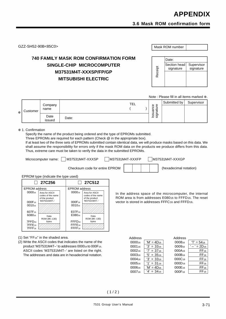
7531 Group User’s Manual 3-71
APPENDIX
GZZ-SH52-90B<85C0>
Checksum code for entire EPROM (hexadecimal notation)
(1) Set “FF16” in the shaded area.(2) Write the ASCII codes that indicates the name of the
product ‘M37531M4T–’ to addresses 000016 to 000F16.ASCII codes ‘M37531M4T–’ are listed on the right.The addresses and data are in hexadecimal notation.
Address000016
000116
000216
000316
000416
000516
000616
000716
‘M’ = 4D16
‘3’ = 3316
‘7’ = 3716
‘5’ = 3516
‘3’ = 3316
‘1’ = 3116
‘M’ = 4D16
‘4’ = 3416
Address000816
000916
000A16
000B16
000C16
000D16
000E16
000F16
‘T’ = 5416
‘ – ’ = 2D16
FF16
FF16
FF16
FF16
FF16
FF16
EPROM type (indicate the type used)
27C256 27C512
000016
000F16
001016
607F16
608016
7FFD16
7FFE16
7FFF16
EPROM addressArea for ASCIIcodes of the nameof the product‘M37531M4T–’
Mask ROM number
1. ConfirmationSpecify the name of the product being ordered and the type of EPROMs submitted.Three EPROMs are required for each pattern (Check @ in the appropriate box).If at least two of the three sets of EPROMs submitted contain identical data, we will produce masks based on this data. Weshall assume the responsibility for errors only if the mask ROM data on the products we produce differs from this data.Thus, extreme care must be taken to verify the data in the submitted EPROMs.
Microcomputer name: M37531M4T-XXXSP M37531M4T-XXXFP M37531M4T-XXXGP
DataROM (8K–130)
bytes
EPROM address 000016
000F16
001016
E07F16
E08016
FFFD16
FFFE16
FFFF16
Area for ASCIIcodes of the nameof the product‘M37531M4T–’
DataROM (8K–130)
bytes
In the address space of the microcomputer, the internalROM area is from addresses E08016 to FFFD16. The resetvector is stored in addresses FFFC16 and FFFD16.
740 FAMILY MASK ROM CONFIRMATION FORM
SINGLE-CHIP MICROCOMPUTER
M37531M4T-XXXSP/FP/GP
MITSUBISHI ELECTRIC
Rec
eipt
Date:
Section headsignature
Supervisorsignature
Companyname
Note : Please fill in all items marked .
Customer
Issu
ance
sign
atur
e
Dateissued
Submitted byTEL( )
Date:
Supervisor
( 1 / 2 )
3.6 Mask ROM confirmation form
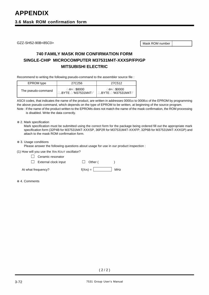
3-72
APPENDIX
7531 Group User’s Manual
= $8000 .BYTE ‘M37531M4T-’
= $0000 .BYTE ‘M37531M4T-’
740 FAMILY MASK ROM CONFIRMATION FORM
SINGLE-CHIP MICROCOMPUTER M37531M4T-XXXSP/FP/GP
MITSUBISHI ELECTRIC
GZZ-SH52-90B<85C0>
Recommend to writing the following pseudo-command to the assembler source file :
27C256 27C512EPROM type
The pseudo-command
ASCII codes, that indicates the name of the product, are written in addresses 000016 to 000816 of the EPROM by programmingthe above pseudo-command, which depends on the type of EPROM to be written, at beginning of the source program.Note : If the name of the product written to the EPROMs does not match the name of the mask confirmation, the ROM processing
is disabled. Write the data correctly.
Mask ROM number
2. Mark specificationMark specification must be submitted using the correct form for the package being ordered fill out the appropriate markspecification form (32P4B for M37531M4T-XXXSP, 36P2R for M37531M4T-XXXFP, 32P6B for M37531M4T-XXXGP) andattach to the mask ROM confirmation form.
3. Usage conditionsPlease answer the following questions about usage for use in our product inspection :
(1) How will you use the XIN-XOUT oscillator?
At what frequency? f(XIN) =
Ceramic resonator
External clock input Other ( )
MHz
4. Comments
( 2 / 2 )
3.6 Mask ROM confirmation form
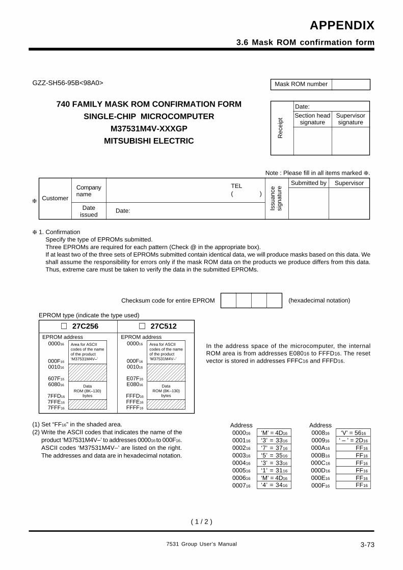
7531 Group User’s Manual 3-73
APPENDIX
GZZ-SH56-95B<98A0>
Checksum code for entire EPROM (hexadecimal notation)
(1) Set “FF16” in the shaded area.(2) Write the ASCII codes that indicates the name of the
product ‘M37531M4V–’ to addresses 000016 to 000F16.ASCII codes ‘M37531M4V–’ are listed on the right.The addresses and data are in hexadecimal notation.
Address000016
000116
000216
000316
000416
000516
000616
000716
‘M’ = 4D16
‘3’ = 3316
‘7’ = 3716
‘5’ = 3516
‘3’ = 3316
‘1’ = 3116
‘M’ = 4D16
‘4’ = 3416
Address000816
000916
000A16
000B16
000C16
000D16
000E16
000F16
‘V’ = 5616
‘ – ’ = 2D16
FF16
FF16
FF16
FF16
FF16
FF16
EPROM type (indicate the type used)
27C256 27C512
000016
000F16
001016
607F16
608016
7FFD16
7FFE16
7FFF16
EPROM addressArea for ASCIIcodes of the nameof the product‘M37531M4V–’
Mask ROM number
1. ConfirmationSpecify the type of EPROMs submitted.Three EPROMs are required for each pattern (Check @ in the appropriate box).If at least two of the three sets of EPROMs submitted contain identical data, we will produce masks based on this data. Weshall assume the responsibility for errors only if the mask ROM data on the products we produce differs from this data.Thus, extreme care must be taken to verify the data in the submitted EPROMs.
DataROM (8K–130)
bytes
EPROM address 000016
000F16
001016
E07F16
E08016
FFFD16
FFFE16
FFFF16
Area for ASCIIcodes of the nameof the product‘M37531M4V–’
DataROM (8K–130)
bytes
In the address space of the microcomputer, the internalROM area is from addresses E08016 to FFFD16. The resetvector is stored in addresses FFFC16 and FFFD16.
740 FAMILY MASK ROM CONFIRMATION FORM
SINGLE-CHIP MICROCOMPUTER
M37531M4V-XXXGP
MITSUBISHI ELECTRIC
Rec
eipt
Date:
Section headsignature
Supervisorsignature
Companyname
Note : Please fill in all items marked .
Customer
Issu
ance
sign
atur
e
Dateissued
Submitted byTEL( )
Date:
Supervisor
( 1 / 2 )
3.6 Mask ROM confirmation form
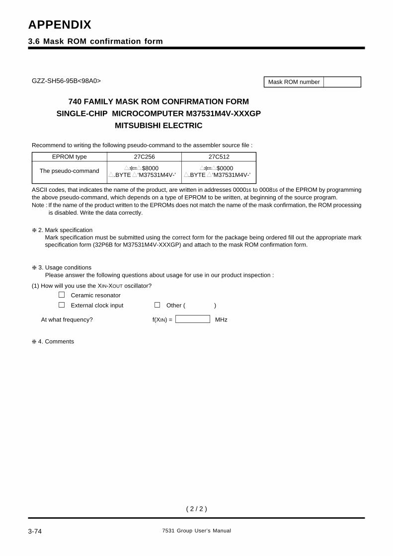
3-74
APPENDIX
7531 Group User’s Manual
= $8000 .BYTE ‘M37531M4V-’
= $0000 .BYTE ‘M37531M4V-’
740 FAMILY MASK ROM CONFIRMATION FORM
SINGLE-CHIP MICROCOMPUTER M37531M4V-XXXGP
MITSUBISHI ELECTRIC
GZZ-SH56-95B<98A0>
Recommend to writing the following pseudo-command to the assembler source file :
27C256 27C512EPROM type
The pseudo-command
ASCII codes, that indicates the name of the product, are written in addresses 000016 to 000816 of the EPROM by programmingthe above pseudo-command, which depends on a type of EPROM to be written, at beginning of the source program.Note : If the name of the product written to the EPROMs does not match the name of the mask confirmation, the ROM processing
is disabled. Write the data correctly.
Mask ROM number
2. Mark specificationMark specification must be submitted using the correct form for the package being ordered fill out the appropriate markspecification form (32P6B for M37531M4V-XXXGP) and attach to the mask ROM confirmation form.
3. Usage conditionsPlease answer the following questions about usage for use in our product inspection :
(1) How will you use the XIN-XOUT oscillator?
At what frequency? f(XIN) =
Ceramic resonator
External clock input Other ( )
MHz
4. Comments
( 2 / 2 )
3.6 Mask ROM confirmation form
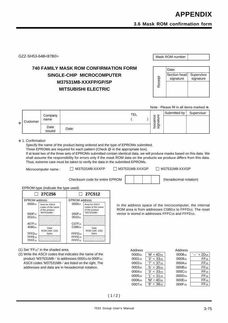
7531 Group User’s Manual 3-75
APPENDIX
GZZ-SH53-64B<87B0>
Checksum code for entire EPROM (hexadecimal notation)
(1) Set “FF16” in the shaded area.(2) Write the ASCII codes that indicates the name of the
product ‘M37531M8–’ to addresses 000016 to 000F16.ASCII codes ‘M37531M8–’ are listed on the right. Theaddresses and data are in hexadecimal notation.
Address000016
000116
000216
000316
000416
000516
000616
000716
‘M’ = 4D16
‘3’ = 3316
‘7’ = 3716
‘5’ = 3516
‘3’ = 3316
‘1’ = 3116
‘M’ = 4D16
‘8’ = 3816
Address000816
000916
000A16
000B16
000C16
000D16
000E16
000F16
‘ – ’ = 2D16
FF16
FF16
FF16
FF16
FF16
FF16
FF16
EPROM type (indicate the type used)
27C256 27C512
000016
000F16
001016
407F16
408016
7FFD16
7FFE16
7FFF16
EPROM addressArea for ASCIIcodes of the nameof the product‘M37531M8–’
Mask ROM number
1. ConfirmationSpecify the name of the product being ordered and the type of EPROMs submitted.Three EPROMs are required for each pattern (Check @ in the appropriate box).If at least two of the three sets of EPROMs submitted contain identical data, we will produce masks based on this data. Weshall assume the responsibility for errors only if the mask ROM data on the products we produce differs from this data.Thus, extreme care must be taken to verify the data in the submitted EPROMs.
Microcomputer name : M37531M8-XXXGPM37531M8-XXXFP M37531M8-XXXSP
DataROM (16K–130)
bytes
EPROM address 000016
000F16
001016
C07F16
C08016
FFFD16
FFFE16
FFFF16
Area for ASCIIcodes of the nameof the product‘M37531M8–’
DataROM (16K–130)
bytes
In the address space of the microcomputer, the internalROM area is from addresses C08016 to FFFD16. The resetvector is stored in addresses FFFC16 and FFFD16.
740 FAMILY MASK ROM CONFIRMATION FORM
SINGLE-CHIP MICROCOMPUTER
M37531M8-XXXFP/GP/SP
MITSUBISHI ELECTRIC
Rec
eipt
Date:
Section headsignature
Supervisorsignature
Companyname
Note : Please fill in all items marked .
Customer
Issu
ance
sign
atur
e
Dateissued
Submitted byTEL( )
Date:
Supervisor
( 1 / 2 )
3.6 Mask ROM confirmation form

3-76
APPENDIX
7531 Group User’s Manual
= $8000 .BYTE ‘M37531M8-’
= $0000 .BYTE ‘M37531M8-’
740 FAMILY MASK ROM CONFIRMATION FORM
SINGLE-CHIP MICROCOMPUTER M37531M8-XXXFP/GP/SP
MITSUBISHI ELECTRIC
GZZ-SH53-64B<87B0>
Recommend to writing the following pseudo-command to the assembler source file :
27C256 27C512EPROM type
The pseudo-command
ASCII codes, that indicates the name of the product, are written in addresses 000016 to 000F16 of the EPROM by programmingthe above pseudo-command, which depends on a type of EPROM to be written, at beginning of the source program.Note : If the name of the product written to the EPROMs does not match the name of the mask confirmation, the ROM processing
is disabled. Write the data correctly.
Mask ROM number
2. Mark specificationMark specification must be submitted using the correct form for the package being ordered fill out the appropriate markspecification form (36P2R for M37531M8-XXXFP, 32P6B for M37531M8-XXXGP, 32P4B for M37531M8-XXXSP) andattach to the mask ROM confirmation form.
3. Usage conditionsPlease answer the following questions about usage for use in our product inspection :
(1) How will you use the XIN-XOUT oscillator?
At what frequency? f(XIN) =
Ceramic resonator
External clock input Other ( )
MHz
4. Comments
( 2 / 2 )
3.6 Mask ROM confirmation form
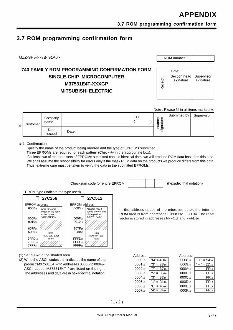
7531 Group User’s Manual 3-77
APPENDIX
GZZ-SH54-78B<91A0>
Checksum code for entire EPROM (hexadecimal notation)
(1) Set “FF16” in the shaded area.(2) Write the ASCII codes that indicates the name of the
product ‘M37531E4T–’ to addresses 000016 to 000F16.ASCII codes ‘M37531E4T–’ are listed on the right.The addresses and data are in hexadecimal notation.
Address000016
000116
000216
000316
000416
000516
000616
000716
‘M’ = 4D16
‘3’ = 3316
‘7’ = 3716
‘5’ = 3516
‘3’ = 3316
‘1’ = 3116
‘E’ = 4516
‘4’ = 3416
Address000816
000916
000A16
000B16
000C16
000D16
000E16
000F16
‘ T ’ = 5416
‘ – ’ = 2D16
FF16
FF16
FF16
FF16
FF16
FF16
EPROM type (indicate the type used)
27C256 27C512
000016
000F16
001016
607F16
608016
7FFD16
7FFE16
7FFF16
EPROM addressArea for ASCIIcodes of the nameof the product‘M37531E4T–’
ROM number
1. ConfirmationSpecify the name of the product being ordered and the type of EPROMs submitted.Three EPROMs are required for each pattern (Check @ in the appropriate box).If at least two of the three sets of EPROMs submitted contain identical data, we will produce ROM data based on this data.We shall assume the responsibility for errors only if the mask ROM data on the products we produce differs from this data.Thus, extreme care must be taken to verify the data in the submitted EPROMs.
DataROM (8K–130)
bytes
EPROM address 000016
000F16
001016
E07F16
E08016
FFFD16
FFFE16
FFFF16
Area for ASCIIcodes of the nameof the product‘M37531E4T–’
DataROM (8K–130)
bytes
In the address space of the microcomputer, the internalROM area is from addresses E08016 to FFFD16. The resetvector is stored in addresses FFFC16 and FFFD16.
740 FAMILY ROM PROGRAMMING CONFIRMATION FORM
SINGLE-CHIP MICROCOMPUTER
M37531E4T-XXXGP
MITSUBISHI ELECTRIC
Rec
eipt
Date:
Section headsignature
Supervisorsignature
Companyname
Note : Please fill in all items marked .
Customer
Issu
ance
sign
atur
e
Dateissued
Submitted byTEL( )
Date:
Supervisor
( 1 / 2 )
3.7 ROM programming confirmation form
3.7 ROM programming confirmation form

3-78
APPENDIX
7531 Group User’s Manual
= $8000 .BYTE ‘M37531E4T-’
= $0000 .BYTE ‘M37531E4T-’
740 FAMILY ROM PROGRAMMING CONFIRMATION FORM
SINGLE-CHIP MICROCOMPUTER M37531E4T-XXXGP
MITSUBISHI ELECTRIC
GZZ-SH54-78B<91A0>
Recommend to writing the following pseudo-command to the assembler source file :
27C256 27C512EPROM type
The pseudo-command
ASCII codes, that indicates the name of the product, are written in addresses 000016 to 000816 of the EPROM by programmingthe above pseudo-command, which depends on a type of EPROM to be written, at beginning of the source program.Note : If the name of the product written to the EPROMs does not match the name of the ROM programming confirmation form,
the ROM processing is disabled. Write the data correctly.
ROM number
2. Mark specificationMark specification must be submitted using the correct form for the package being ordered fill out the appropriate markspecification form (32P6B for M37531E4T-XXXGP) and attach to the ROM programming confirmation form.
3. Usage conditionsPlease answer the following questions about usage for use in our product inspection :
(1) How will you use the XIN-XOUT oscillator?
At what frequency? f(XIN) =
Ceramic resonator
External clock input Other ( )
MHz
4. Comments
( 2 / 2 )
3.7 ROM programming confirmation form
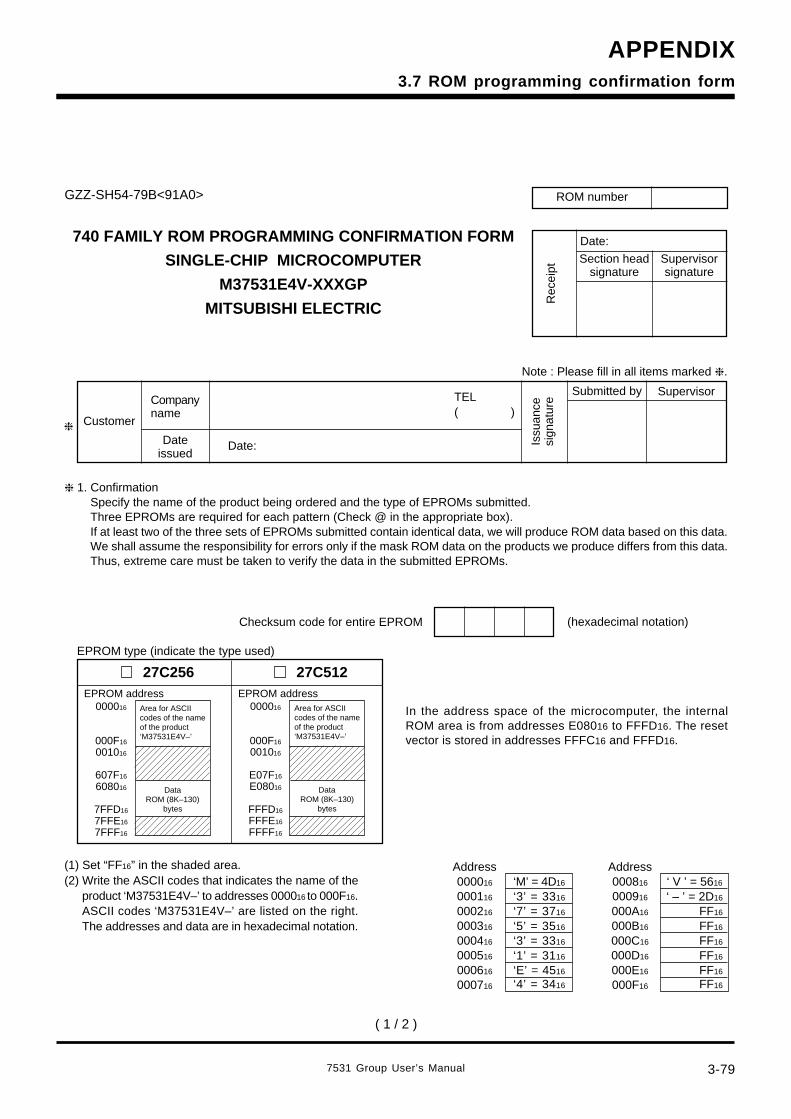
7531 Group User’s Manual 3-79
APPENDIX
GZZ-SH54-79B<91A0>
Checksum code for entire EPROM (hexadecimal notation)
(1) Set “FF16” in the shaded area.(2) Write the ASCII codes that indicates the name of the
product ‘M37531E4V–’ to addresses 000016 to 000F16.ASCII codes ‘M37531E4V–’ are listed on the right.The addresses and data are in hexadecimal notation.
Address000016
000116
000216
000316
000416
000516
000616
000716
‘M’ = 4D16
‘3’ = 3316
‘7’ = 3716
‘5’ = 3516
‘3’ = 3316
‘1’ = 3116
‘E’ = 4516
‘4’ = 3416
Address000816
000916
000A16
000B16
000C16
000D16
000E16
000F16
‘ V ’ = 5616
‘ – ’ = 2D16
FF16
FF16
FF16
FF16
FF16
FF16
EPROM type (indicate the type used)
27C256 27C512
000016
000F16
001016
607F16
608016
7FFD16
7FFE16
7FFF16
EPROM addressArea for ASCIIcodes of the nameof the product‘M37531E4V–’
ROM number
1. ConfirmationSpecify the name of the product being ordered and the type of EPROMs submitted.Three EPROMs are required for each pattern (Check @ in the appropriate box).If at least two of the three sets of EPROMs submitted contain identical data, we will produce ROM data based on this data.We shall assume the responsibility for errors only if the mask ROM data on the products we produce differs from this data.Thus, extreme care must be taken to verify the data in the submitted EPROMs.
DataROM (8K–130)
bytes
EPROM address 000016
000F16
001016
E07F16
E08016
FFFD16
FFFE16
FFFF16
Area for ASCIIcodes of the nameof the product‘M37531E4V–’
DataROM (8K–130)
bytes
In the address space of the microcomputer, the internalROM area is from addresses E08016 to FFFD16. The resetvector is stored in addresses FFFC16 and FFFD16.
740 FAMILY ROM PROGRAMMING CONFIRMATION FORM
SINGLE-CHIP MICROCOMPUTER
M37531E4V-XXXGP
MITSUBISHI ELECTRIC
Rec
eipt
Date:
Section headsignature
Supervisorsignature
Companyname
Note : Please fill in all items marked .
Customer
Issu
ance
sign
atur
e
Dateissued
Submitted byTEL( )
Date:
Supervisor
( 1 / 2 )
3.7 ROM programming confirmation form
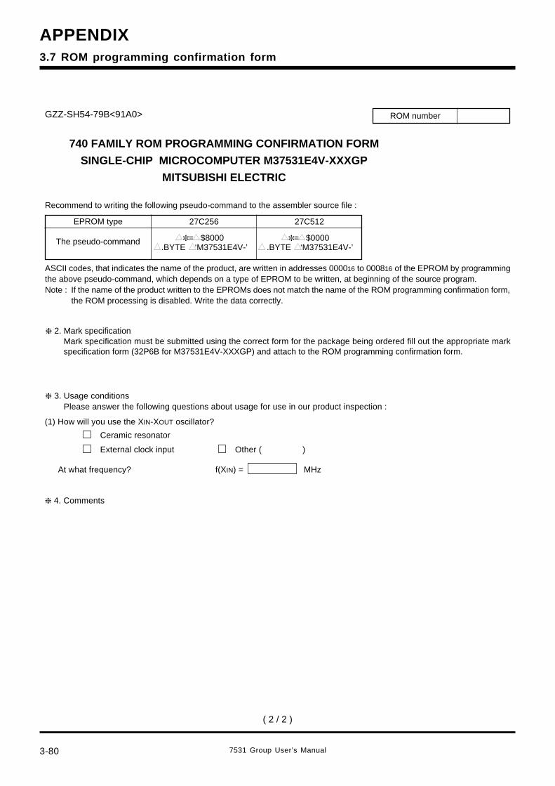
3-80
APPENDIX
7531 Group User’s Manual
= $8000 .BYTE ‘M37531E4V-’
= $0000 .BYTE ‘M37531E4V-’
740 FAMILY ROM PROGRAMMING CONFIRMATION FORM
SINGLE-CHIP MICROCOMPUTER M37531E4V-XXXGP
MITSUBISHI ELECTRIC
GZZ-SH54-79B<91A0>
Recommend to writing the following pseudo-command to the assembler source file :
27C256 27C512EPROM type
The pseudo-command
ASCII codes, that indicates the name of the product, are written in addresses 000016 to 000816 of the EPROM by programmingthe above pseudo-command, which depends on a type of EPROM to be written, at beginning of the source program.Note : If the name of the product written to the EPROMs does not match the name of the ROM programming confirmation form,
the ROM processing is disabled. Write the data correctly.
ROM number
2. Mark specificationMark specification must be submitted using the correct form for the package being ordered fill out the appropriate markspecification form (32P6B for M37531E4V-XXXGP) and attach to the ROM programming confirmation form.
3. Usage conditionsPlease answer the following questions about usage for use in our product inspection :
(1) How will you use the XIN-XOUT oscillator?
At what frequency? f(XIN) =
Ceramic resonator
External clock input Other ( )
MHz
4. Comments
( 2 / 2 )
3.7 ROM programming confirmation form
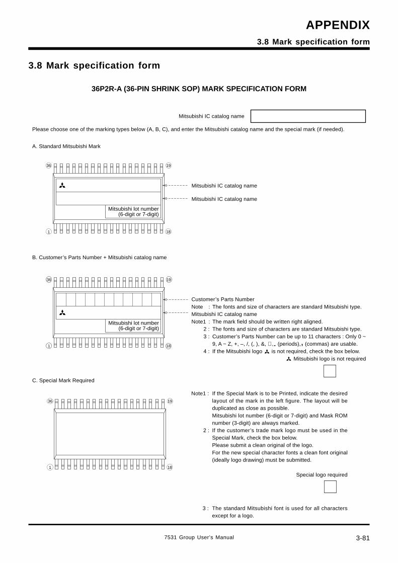
7531 Group User’s Manual 3-81
APPENDIX
3.8 Mark specification form
36P2R-A (36-PIN SHRINK SOP) MARK SPECIFICATION FORM
Mitsubishi IC catalog name
Please choose one of the marking types below (A, B, C), and enter the Mitsubishi catalog name and the special mark (if needed).
A. Standard Mitsubishi Mark
C. Special Mark Required
B. Customer’s Parts Number + Mitsubishi catalog name
Mitsubishi IC catalog name
3 : The standard Mitsubishi font is used for all charactersexcept for a logo.
Note1 : If the Special Mark is to be Printed, indicate the desiredlayout of the mark in the left figure. The layout will beduplicated as close as possible.Mitsubishi lot number (6-digit or 7-digit) and Mask ROMnumber (3-digit) are always marked.
2 : If the customer’s trade mark logo must be used in theSpecial Mark, check the box below.Please submit a clean original of the logo.For the new special character fonts a clean font original(ideally logo drawing) must be submitted.
Special logo required
Customer’s Parts NumberNote : The fonts and size of characters are standard Mitsubishi type.Mitsubishi IC catalog nameNote1 : The mark field should be written right aligned.
2 : The fonts and size of characters are standard Mitsubishi type.3 : Customer’s Parts Number can be up to 11 characters : Only 0 ~
9, A ~ Z, +, –, /, (, ), &, ,. (periods),, (commas) are usable.4 : If the Mitsubishi logo is not required, check the box below.
Mitsubishi logo is not required
Mitsubishi lot number(6-digit or 7-digit)
1 18
1936
Mitsubishi lot number(6-digit or 7-digit)
1 18
1936
1 18
1936
3.8 Mark specification form
Mitsubishi IC catalog name
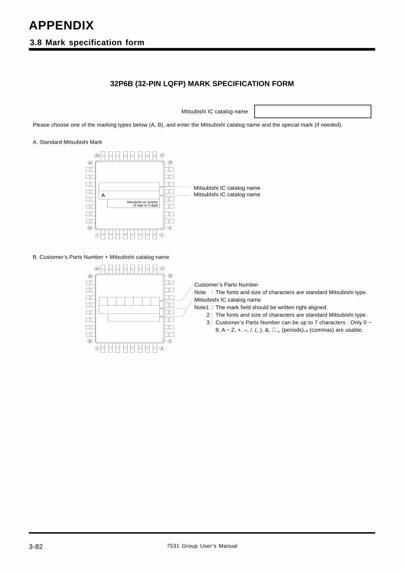
3-82
APPENDIX
7531 Group User’s Manual
32P6B (32-PIN LQFP) MARK SPECIFICATION FORM
Mitsubishi IC catalog name
Please choose one of the marking types below (A, B), and enter the Mitsubishi catalog name and the special mark (if needed).
A. Standard Mitsubishi Mark
B. Customer’s Parts Number + Mitsubishi catalog name
Mitsubishi IC catalog nameMitsubishi IC catalog name
Customer’s Parts NumberNote : The fonts and size of characters are standard Mitsubishi type.Mitsubishi IC catalog nameNote1 : The mark field should be written right aligned.
2 : The fonts and size of characters are standard Mitsubishi type.3 : Customer’s Parts Number can be up to 7 characters : Only 0 ~
9, A ~ Z, +, –, /, (, ), &, ,. (periods),, (commas) are usable.
1
32
8
9
1625
1724
Mitsubishi lot number(4-digit or 5-digit)
1
32
8
9
1625
1724
3.8 Mark specification form
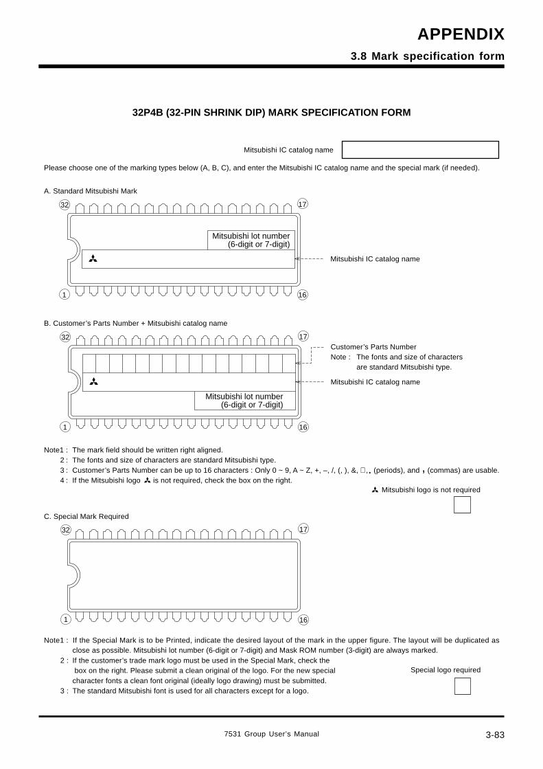
7531 Group User’s Manual 3-83
APPENDIX
32P4B (32-PIN SHRINK DIP) MARK SPECIFICATION FORM
Mitsubishi IC catalog name
Please choose one of the marking types below (A, B, C), and enter the Mitsubishi IC catalog name and the special mark (if needed).
A. Standard Mitsubishi Mark
Note1 : If the Special Mark is to be Printed, indicate the desired layout of the mark in the upper figure. The layout will be duplicated asclose as possible. Mitsubishi lot number (6-digit or 7-digit) and Mask ROM number (3-digit) are always marked.
2 : If the customer’s trade mark logo must be used in the Special Mark, check the box on the right. Please submit a clean original of the logo. For the new specialcharacter fonts a clean font original (ideally logo drawing) must be submitted.
3 : The standard Mitsubishi font is used for all characters except for a logo.
Special logo required
Mitsubishi IC catalog name
C. Special Mark Required
B. Customer’s Parts Number + Mitsubishi catalog name
Customer’s Parts NumberNote : The fonts and size of characters
are standard Mitsubishi type.
Mitsubishi IC catalog name
Note1 : The mark field should be written right aligned.2 : The fonts and size of characters are standard Mitsubishi type.3 : Customer’s Parts Number can be up to 16 characters : Only 0 ~ 9, A ~ Z, +, –, /, (, ), &, ,. (periods), and , (commas) are usable.4 : If the Mitsubishi logo is not required, check the box on the right.
Mitsubishi logo is not required
Mitsubishi lot number(6-digit or 7-digit)
32
1 16
17
Mitsubishi lot number(6-digit or 7-digit)
32
1 16
17
32
1 16
17
3.8 Mark specification form
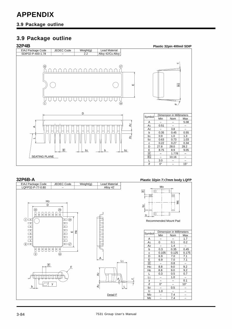
3-84
APPENDIX
7531 Group User’s Manual
3.9 Package outline
3.9 Package outline
SDIP32-P-400-1.78Weight(g)
– 2.2JEDEC CodeEIAJ Package Code Lead Material
Alloy 42/Cu Alloy
32P4B Plastic 32pin 400mil SDIP
SymbolMin Nom Max
A
A2
bb1
b2
c
ED
L
Dimension in Millimeters
A1 0.51 – –– 3.8 –
0.35 0.45 0.550.9 1.0 1.30.63 0.73 1.030.22 0.27 0.34
27.8 28.0 28.28.75 8.9 9.05– 1.778 –– 10.16 –
3.0 – –0° – 15°
– – 5.08
ee1
32 17
161
E
ce1
A2
A1
b2bb1e
LA
SEATING PLANE
D
LQFP32-P-77-0.80Weight(g)
–JEDEC CodeEIAJ Package Code Lead Material
Alloy 42
32P6B-A Plastic 32pin 77mm body LQFP
–0.1
–
– –0.2
––
– –––
––
–
SymbolMin Nom Max
A
A2
bcDE
HE
LL1y
b2
Dimension in Millimeters
HD
A1
0.5––I2 1.0––MD 7.4––ME 7.4
10°0°0.1
1.00.70.50.39.29.08.89.29.08.8
0.87.17.06.97.17.06.90.1750.1250.1050.450.350.3
1.40
1.7
e
e
e
E
c
HE
1
8
9
32 25
24
16
17
HD
D
MD
ME
A
F
b A1
A2
L1
Ly
b2
I2
Recommended Mount Pad
Detail F
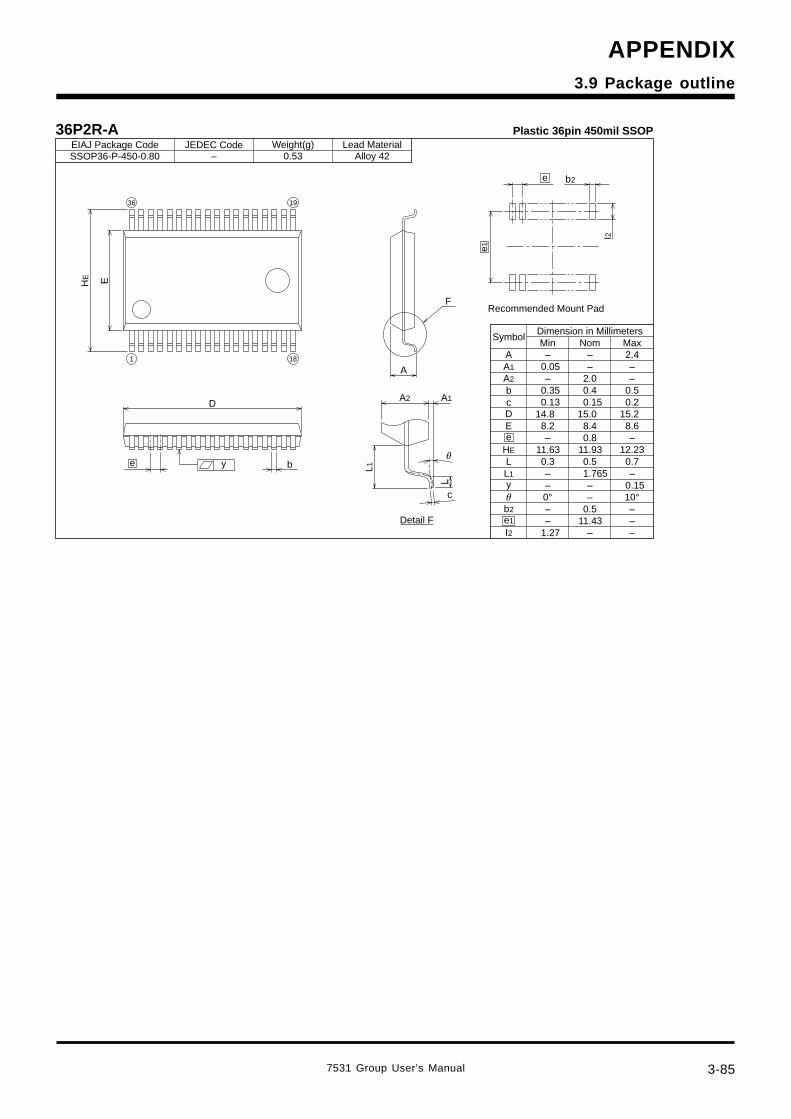
7531 Group User’s Manual 3-85
APPENDIX3.9 Package outline
SSOP36-P-450-0.80Weight(g)
–JEDEC Code
0.53EIAJ Package Code Lead Material
Alloy 42
36P2R-A Plastic 36pin 450mil SSOP
SymbolMin Nom Max
A
A2
bcDE
LL1y
Dimension in Millimeters
HE
A1
I2
–
–.350
.050
.130
.814
.28–.6311.30––
–.271
––
.02
.40
.150
.015
.48
.80
.9311
.50
.7651–
.4311–
–.42
–.50.20.215.68–.2312.70–.150
–b2 – .50 –
–
0° – 10°
e
e1
36 19
181
HE E
D
be y
F
A
A2 A1
L1
L
c
e b2
e1
I2
Recommended Mount Pad
Detail F
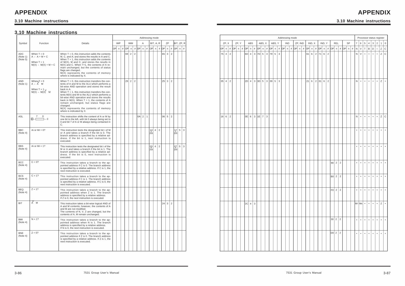
Addressing mode
ZP, X ZP, Y ABS ABS, X ABS, Y IND ZP, IND IND, X IND, Y REL SP 7 6 5 4 3 2 1 0
Processor status register
N V T B D I Z COP n # OP n # OP n # OP n # OP n # OP n # OP n # OP n #OP n # OP n # OP n #
7531 Group User’s Manual 3-87
APPENDIX3.10 Machine instructions
Addressing mode
Symbol Function Details IMP IMM A BIT, A ZP BIT, ZP
OP n # OP n # OP n # OP n # OP n #OP n #
3-86
APPENDIX
7531 Group User’s Manual
3.10 Machine instructions
75
35
16
4
4
6
2
2
2
6D
2D
0E
2C
4
4
6
4
3
3
3
3
7D
3D
1E
5
5
7
3
3
3
79
39
5
5
3
3
61
21
6
6
2
2
90
B0
F0
2
2
2
2
2
2
71
31
6
6
2
2
N
N
N
•
•
•
•
•
M7
•
•
V
•
•
•
•
•
•
•
M6
•
•
•
•
•
•
•
•
•
•
•
•
•
•
•
•
•
•
•
•
•
•
•
•
•
•
•
•
•
•
•
•
•
•
•
•
•
•
•
•
•
•
•
•
•
•
Z
Z
Z
•
•
•
•
•
Z
•
•
C
•
C
•
•
•
•
•
•
•
•
When T = 0, this instruction adds the contentsM, C, and A; and stores the results in A and C.When T = 1, this instruction adds the contentsof M(X), M and C; and stores the results inM(X) and C. When T=1, the contents of A re-main unchanged, but the contents of statusflags are changed.M(X) represents the contents of memorywhere is indicated by X.
When T = 0, this instruction transfers the con-tents of A and M to the ALU which performs abit-wise AND operation and stores the resultback in A.When T = 1, this instruction transfers the con-tents M(X) and M to the ALU which performs abit-wise AND operation and stores the resultsback in M(X). When T = 1, the contents of Aremain unchanged, but status flags arechanged.M(X) represents the contents of memorywhere is indicated by X.
This instruction shifts the content of A or M byone bit to the left, with bit 0 always being set to0 and bit 7 of A or M always being contained inC.
This instruction tests the designated bit i of Mor A and takes a branch if the bit is 0. Thebranch address is specified by a relative ad-dress. If the bit is 1, next instruction isexecuted.
This instruction tests the designated bit i of theM or A and takes a branch if the bit is 1. Thebranch address is specified by a relative ad-dress. If the bit is 0, next instruction isexecuted.
This instruction takes a branch to the ap-pointed address if C is 0. The branch addressis specified by a relative address. If C is 1, thenext instruction is executed.
This instruction takes a branch to the ap-pointed address if C is 1. The branch addressis specified by a relative address. If C is 0, thenext instruction is executed.
This instruction takes a branch to the ap-pointed address when Z is 1. The branchaddress is specified by a relative address.If Z is 0, the next instruction is executed.
This instruction takes a bit-wise logical AND ofA and M contents; however, the contents of Aand M are not modified.The contents of N, V, Z are changed, but thecontents of A, M remain unchanged.
This instruction takes a branch to the ap-pointed address when N is 1. The branchaddress is specified by a relative address.If N is 0, the next instruction is executed.
This instruction takes a branch to the ap-pointed address if Z is 0. The branch addressis specified by a relative address. If Z is 1, thenext instruction is executed.
ADC(Note 1)(Note 5)
AND(Note 1)
ASL
BBC(Note 4)
BBS(Note 4)
BCC(Note 4)
BCS(Note 4)
BEQ(Note 4)
BIT
BMI(Note 4)
BNE(Note 4)
7 0C← ←0
29 2 2
0A 2 1
03+20i
17+20i
07+20i
06 5 2
25 3 2
3
65 3 269 2 2
4
4
2
2
13+20i
5
5
3
3
24
When T = 0A ← A + M + C
When T = 1M(X) ← M(X) + M + C
When T = 0A ← A M
When T = 1M(X) ← M(X) M
Ai or Mi = 0?
Ai or Mi = 1?
C = 0?
C = 1?
Z = 1?
A M
N = 1?
Z = 0?
V
V
V
2
3.10 Machine instructions
BIT, A, R BIT, ZP, R
30
D0
2
2
2
2
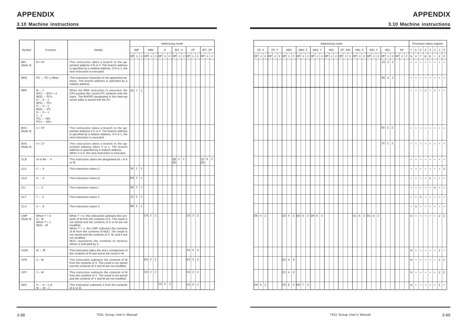
Addressing mode
ZP, X ZP, Y ABS ABS, X ABS, Y IND ZP, IND IND, X IND, Y REL SP 7 6 5 4 3 2 1 0
Processor status register
N V T B D I Z COP n # OP n # OP n # OP n # OP n # OP n # OP n # OP n #OP n # OP n # OP n #
7531 Group User’s Manual 3-89
APPENDIX3.10 Machine instructions
Addressing mode
Symbol Function Details IMP IMM A BIT, A ZP BIT, ZP
OP n # OP n # OP n # OP n # OP n #OP n #
3-88
APPENDIX
7531 Group User’s Manual
3.10 Machine instructions
D5
D6
CD
EC
CC
CE
50
70
2
2
2
2
•
•
•
•
•
•
•
•
•
•
•
N
N
N
N
N
•
•
•
•
•
•
•
•
•
•
0
•
•
•
•
•
4
6
4
4
4
6
3
3
3
3
DD
DE
5
7
3
3
D9 5 3 C1 6 2 D1 6 2
•
•
•
•
•
•
•
•
•
0
•
•
•
•
•
•
•
•
1
•
•
•
•
•
•
•
•
•
•
•
•
•
•
•
•
•
•
•
•
0
•
•
•
•
•
•
•
•
•
•
1
•
•
•
•
•
0
•
•
•
•
•
•
•
•
•
•
•
•
•
•
•
•
•
•
Z
Z
Z
Z
Z
•
•
•
•
•
•
0
•
•
•
•
C
•
C
C
•
2
2
This instruction takes a branch to the ap-pointed address if N is 0. The branch addressis specified by a relative address. If N is 1, thenext instruction is executed.
This instruction branches to the appointed ad-dress. The branch address is specified by arelative address.
When the BRK instruction is executed, theCPU pushes the current PC contents onto thestack. The BADRS designated in the interruptvector table is stored into the PC.
This instruction takes a branch to the ap-pointed address if V is 0. The branch addressis specified by a relative address. If V is 1, thenext instruction is executed.
This instruction takes a branch to the ap-pointed address when V is 1. The branchaddress is specified by a relative address.When V is 0, the next instruction is executed.
This instruction clears the designated bit i of Aor M.
This instruction clears C.
This instruction clears D.
This instruction clears I.
This instruction clears T.
This instruction clears V.
When T = 0, this instruction subtracts the con-tents of M from the contents of A. The result isnot stored and the contents of A or M are notmodified.When T = 1, the CMP subtracts the contentsof M from the contents of M(X). The result isnot stored and the contents of X, M, and A arenot modified.M(X) represents the contents of memorywhere is indicated by X.
This instruction takes the one’s complement ofthe contents of M and stores the result in M.
This instruction subtracts the contents of Mfrom the contents of X. The result is not storedand the contents of X and M are not modified.
This instruction subtracts the contents of Mfrom the contents of Y. The result is not storedand the contents of Y and M are not modified.
This instruction subtracts 1 from the contentsof A or M.
BPL(Note 4)
BRA
BRK
BVC(Note 4)
BVS(Note 4)
CLB
CLC
CLD
CLI
CLT
CLV
CMP(Note 3)
COM
CPX
CPY
DEC
N = 0?
PC ← PC ± offset
B ← 1(PC) ← (PC) + 2M(S) ← PCHS ← S – 1M(S) ← PCLS ← S – 1M(S) ← PSS ← S – 1I← 1PCL ← ADLPCH ← ADH
V = 0?
V = 1?
Ai or Mi ← 0
C ← 0
D ← 0
I ← 0
T ← 0
V ← 0
When T = 0A – MWhen T = 1M(X) – M
__
M ← M
X – M
Y – M
A ← A – 1 orM ← M – 1
18
D8
58
12
B8
2
2
2
2
2
1
1
1
1
1
C9
E0
C0
2
2
2
2
2
2
1A 2 1
1B+20i
C5
44
E4
C4
C6
3
5
3
3
5
2
2
2
2
2
1F+20i
2 1 5 2
00 7 1
10
80
2
4
2
2
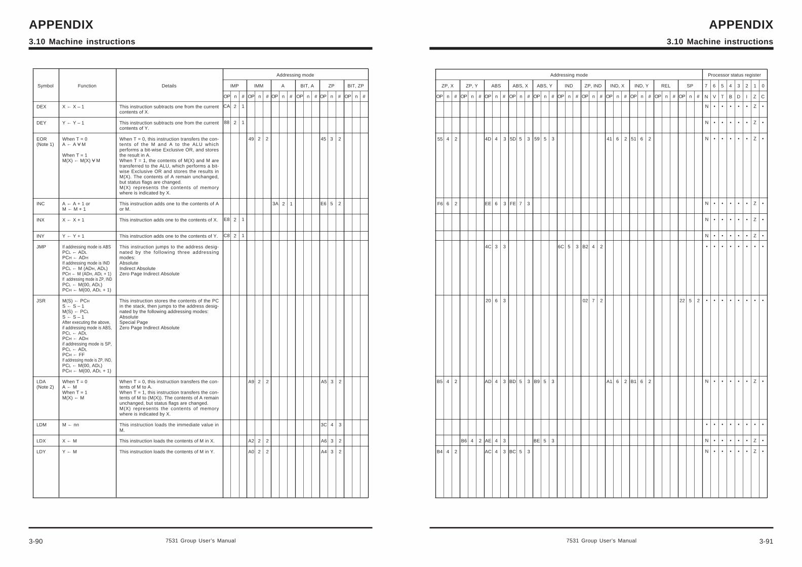
Addressing mode
ZP, X ZP, Y ABS ABS, X ABS, Y IND ZP, IND IND, X IND, Y REL SP 7 6 5 4 3 2 1 0
Processor status register
N V T B D I Z COP n # OP n # OP n # OP n # OP n # OP n # OP n # OP n #OP n # OP n # OP n #
7531 Group User’s Manual 3-91
APPENDIX3.10 Machine instructions
Addressing mode
Symbol Function Details IMP IMM A BIT, A ZP BIT, ZP
OP n # OP n # OP n # OP n # OP n #OP n #
3-90
APPENDIX
7531 Group User’s Manual
3.10 Machine instructions
This instruction subtracts one from the currentcontents of X.
This instruction subtracts one from the currentcontents of Y.
When T = 0, this instruction transfers the con-tents of the M and A to the ALU whichperforms a bit-wise Exclusive OR, and storesthe result in A.When T = 1, the contents of M(X) and M aretransferred to the ALU, which performs a bit-wise Exclusive OR and stores the results inM(X). The contents of A remain unchanged,but status flags are changed.M(X) represents the contents of memorywhere is indicated by X.
This instruction adds one to the contents of Aor M.
This instruction adds one to the contents of X.
This instruction adds one to the contents of Y.
This instruction jumps to the address desig-nated by the following three addressingmodes:AbsoluteIndirect AbsoluteZero Page Indirect Absolute
This instruction stores the contents of the PCin the stack, then jumps to the address desig-nated by the following addressing modes:AbsoluteSpecial PageZero Page Indirect Absolute
When T = 0, this instruction transfers the con-tents of M to A.When T = 1, this instruction transfers the con-tents of M to (M(X)). The contents of A remainunchanged, but status flags are changed.M(X) represents the contents of memorywhere is indicated by X.
This instruction loads the immediate value inM.
This instruction loads the contents of M in X.
This instruction loads the contents of M in Y.
DEX
DEY
EOR(Note 1)
INC
INX
INY
JMP
JSR
LDA(Note 2)
LDM
LDX
LDY
X ← X – 1
Y ← Y – 1
When T = 0A ← A V– M
When T = 1M(X) ← M(X) V– M
A ← A + 1 orM ← M + 1
X ← X + 1
Y ← Y + 1
If addressing mode is ABSPCL ← ADLPCH ← ADHIf addressing mode is INDPCL ← M (ADH, ADL)PCH ← M (ADH, ADL + 1)If addressing mode is ZP, INDPCL ← M(00, ADL)PCH ← M(00, ADL + 1)
M(S) ← PCHS ← S – 1M(S) ← PCLS ← S – 1After executing the above,if addressing mode is ABS,PCL ← ADLPCH ← ADHif addressing mode is SP,PCL ← ADLPCH ← FFIf addressing mode is ZP, IND,PCL ← M(00, ADL)PCH ← M(00, ADL + 1)
When T = 0A ← MWhen T = 1M(X) ← M
M ← nn
X ← M
Y ← M
3A 2 1
1
1
1
1
2
2
2
2
CA
88
E8
C8
45
E6
3
5
2
2
49 2 2 55
F6
4
6
2
2
4D
EE
4
6
3
3
5D
FE
5
7
3
3
59 5 3
N
N
N
N
N
N
•
•
N
•
N
N
•
•
•
•
•
•
•
•
•
•
•
•
•
•
•
•
•
•
•
•
•
•
•
•
•
•
•
•
•
•
•
•
•
•
•
•
•
•
•
•
•
•
•
•
•
•
•
•
•
•
•
•
•
•
•
•
•
•
•
•
Z
Z
Z
Z
Z
Z
•
•
Z
•
Z
Z
•
•
•
•
•
•
•
•
•
•
•
•
41 6 2 51 6 2
B5
B4
4C
20
AD
AE
AC
6C
A14
4
2
2
B6 4 2
3
6
4
4
4
3
3
3
3
3
BD
BC
5
5
B9
BE
5
5
3
3
3
3
5 3 B2
02
4
7
2
2
6 2 B1 6 2
22 5 2
A9
A2
A0
A5
3C
A6
A4
3
4
3
3
2
3
2
2
2
2
2
2
2
2
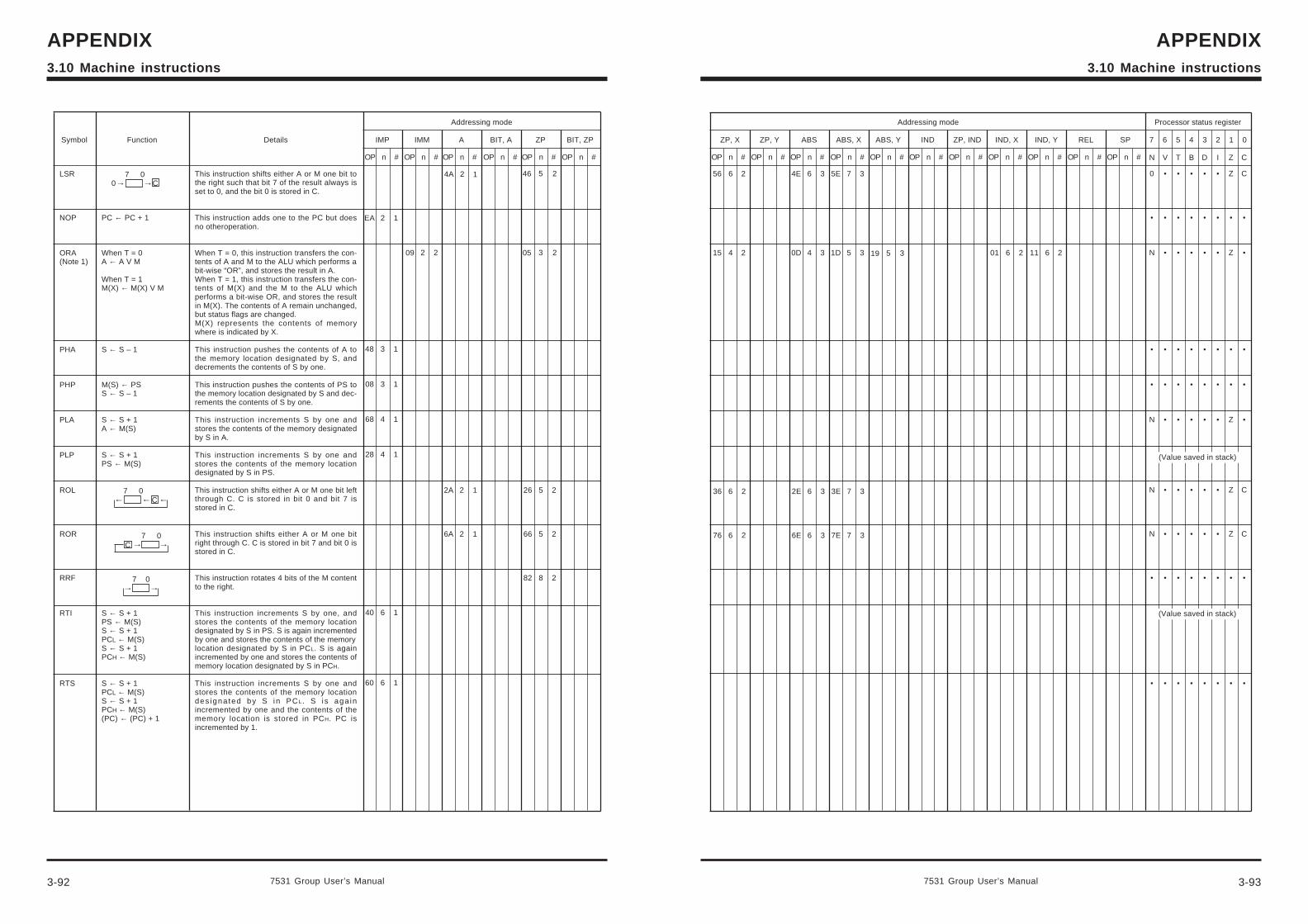
Addressing mode
ZP, X ZP, Y ABS ABS, X ABS, Y IND ZP, IND IND, X IND, Y REL SP 7 6 5 4 3 2 1 0
Processor status register
N V T B D I Z COP n # OP n # OP n # OP n # OP n # OP n # OP n # OP n #OP n # OP n # OP n #
7531 Group User’s Manual 3-93
APPENDIX3.10 Machine instructions
Addressing mode
Symbol Function Details IMP IMM A BIT, A ZP BIT, ZP
OP n # OP n # OP n # OP n # OP n #OP n #
3-92
APPENDIX
7531 Group User’s Manual
3.10 Machine instructions
0
•
N
•
•
N
N
N
•
•
•
•
•
•
•
•
•
•
•
•
•
•
•
•
•
•
•
•
•
•
•
•
•
•
•
•
•
•
•
•
•
•
•
•
•
•
•
•
•
•
•
•
•
•
•
•
•
•
•
•
Z
•
Z
•
•
Z
Z
Z
•
•
C
•
•
•
•
•
C
C
•
•
This instruction shifts either A or M one bit tothe right such that bit 7 of the result always isset to 0, and the bit 0 is stored in C.
This instruction adds one to the PC but doesno otheroperation.
When T = 0, this instruction transfers the con-tents of A and M to the ALU which performs abit-wise “OR”, and stores the result in A.When T = 1, this instruction transfers the con-tents of M(X) and the M to the ALU whichperforms a bit-wise OR, and stores the resultin M(X). The contents of A remain unchanged,but status flags are changed.M(X) represents the contents of memorywhere is indicated by X.
This instruction pushes the contents of A tothe memory location designated by S, anddecrements the contents of S by one.
This instruction pushes the contents of PS tothe memory location designated by S and dec-rements the contents of S by one.
This instruction increments S by one andstores the contents of the memory designatedby S in A.
This instruction increments S by one andstores the contents of the memory locationdesignated by S in PS.
This instruction shifts either A or M one bit leftthrough C. C is stored in bit 0 and bit 7 isstored in C.
This instruction shifts either A or M one bitright through C. C is stored in bit 7 and bit 0 isstored in C.
This instruction rotates 4 bits of the M contentto the right.
This instruction increments S by one, andstores the contents of the memory locationdesignated by S in PS. S is again incrementedby one and stores the contents of the memorylocation designated by S in PCL. S is againincremented by one and stores the contents ofmemory location designated by S in PCH.
This instruction increments S by one andstores the contents of the memory locationdes igna ted by S in PCL. S i s aga inincremented by one and the contents of thememory location is stored in PCH. PC isincremented by 1.
LSR
NOP
ORA(Note 1)
PHA
PHP
PLA
PLP
ROL
ROR
RRF
RTI
RTS
PC ← PC + 1
When T = 0A ← A V M
When T = 1M(X) ← M(X) V M
S ← S – 1
M(S) ← PSS ← S – 1
S ← S + 1A ← M(S)
S ← S + 1PS ← M(S)
S ← S + 1PS ← M(S)S ← S + 1PCL ← M(S)S ← S + 1PCH ← M(S)
S ← S + 1PCL ← M(S)S ← S + 1PCH ← M(S)(PC) ← (PC) + 1
7 0← ←C ←
7 0→ →
7 0 C → →
7 00→ →C
4A 2 1
EA 2 1
09 2 2
46
05
5
3
2
2
2A
6A
26
66
82
48
08
68
28
40
60
3
3
4
4
6
6
1
1
1
1
1
1
2
2
1
1
5
5
8
2
2
2
56
15
6
4
2
2
4E
0D
6
4
3
3
5E
1D
7
5
3
3 19 5 3 01 6 2 11 6 2
36
76
2E
6E
6
6
2
2
6
6
3
3
3E
7E
7
7
3
3
(Value saved in stack)
(Value saved in stack)
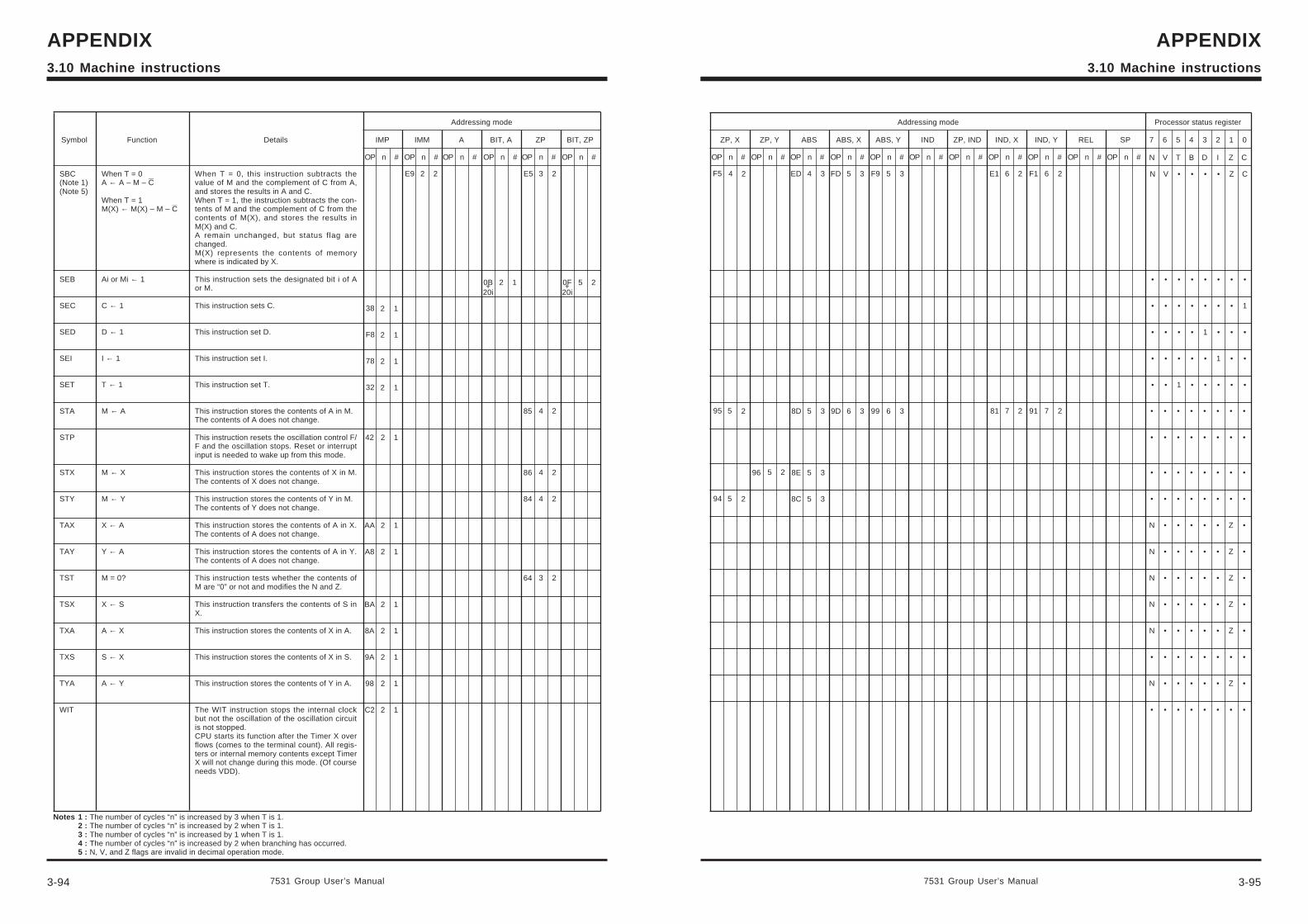
Addressing mode
ZP, X ZP, Y ABS ABS, X ABS, Y IND ZP, IND IND, X IND, Y REL SP 7 6 5 4 3 2 1 0
Processor status register
N V T B D I Z COP n # OP n # OP n # OP n # OP n # OP n # OP n # OP n #OP n # OP n # OP n #
7531 Group User’s Manual 3-95
APPENDIX3.10 Machine instructions
Addressing mode
Symbol Function Details IMP IMM A BIT, A ZP BIT, ZP
OP n # OP n # OP n # OP n # OP n #OP n #
3-94
APPENDIX
7531 Group User’s Manual
3.10 Machine instructions
•
•
•
•
N
N
N
N
N
•
N
•
•
•
•
•
•
•
•
•
•
•
•
•
•
•
•
•
•
•
•
•
•
•
•
•
•
•
•
•
•
•
•
•
•
•
•
•
•
•
•
•
•
•
•
•
•
•
•
•
•
•
•
•
•
•
•
•
•
•
•
•
•
•
•
•
Z
Z
Z
Z
Z
•
Z
•
•
•
•
•
•
•
•
•
•
•
•
•
When T = 0, this instruction subtracts thevalue of M and the complement of C from A,and stores the results in A and C.When T = 1, the instruction subtracts the con-tents of M and the complement of C from thecontents of M(X), and stores the results inM(X) and C.A remain unchanged, but status flag arechanged.M(X) represents the contents of memorywhere is indicated by X.
This instruction sets the designated bit i of Aor M.
This instruction sets C.
This instruction set D.
This instruction set I.
This instruction set T.
This instruction stores the contents of A in M.The contents of A does not change.
This instruction resets the oscillation control F/F and the oscillation stops. Reset or interruptinput is needed to wake up from this mode.
This instruction stores the contents of X in M.The contents of X does not change.
This instruction stores the contents of Y in M.The contents of Y does not change.
This instruction stores the contents of A in X.The contents of A does not change.
This instruction stores the contents of A in Y.The contents of A does not change.
This instruction tests whether the contents ofM are “0” or not and modifies the N and Z.
This instruction transfers the contents of S inX.
This instruction stores the contents of X in A.
This instruction stores the contents of X in S.
This instruction stores the contents of Y in A.
The WIT instruction stops the internal clockbut not the oscillation of the oscillation circuitis not stopped.CPU starts its function after the Timer X overflows (comes to the terminal count). All regis-ters or internal memory contents except TimerX will not change during this mode. (Of courseneeds VDD).
SBC(Note 1)(Note 5)
SEB
SEC
SED
SEI
SET
STA
STP
STX
STY
TAX
TAY
TST
TSX
TXA
TXS
TYA
WIT
When T = 0 _
A ← A – M – C
When T = 1 _
M(X) ← M(X) – M – C
Ai or Mi ← 1
C ← 1
D ← 1
I ← 1
T ← 1
M ← A
M ← X
M ← Y
X ← A
Y ← A
M = 0?
X ← S
A ← X
S ← X
A ← Y
85
86
84
64
4
4
4
3
2
2
2
2
Notes 1 : The number of cycles “n” is increased by 3 when T is 1.2 : The number of cycles “n” is increased by 2 when T is 1.3 : The number of cycles “n” is increased by 1 when T is 1.4 : The number of cycles “n” is increased by 2 when branching has occurred.5 : N, V, and Z flags are invalid in decimal operation mode.
33 5FD4ED24F5 F9 5 3 E1 6 2 F1 6 2E9 2 2
0B+20i
0F+20i
2 1 5 2
E5 3 2
38
F8
78
32
2
2
2
2
1
1
1
1
42
AA
A8
BA
8A
9A
98
C2
2
2
2
2
2
2
2
2
1
1
1
1
1
1
1
1
95
94
5
5
2
2
96 5 2
8D
8E
8C
5
5
5
3
3
3
9D 6 3 99 6 3 81 7 2 91 7 2
N
•
•
•
•
•
V
•
•
•
•
•
•
•
•
•
•
1
•
•
•
•
•
•
•
•
•
1
•
•
•
•
•
•
1
•
Z
•
•
•
•
•
C
•
1
•
•
•
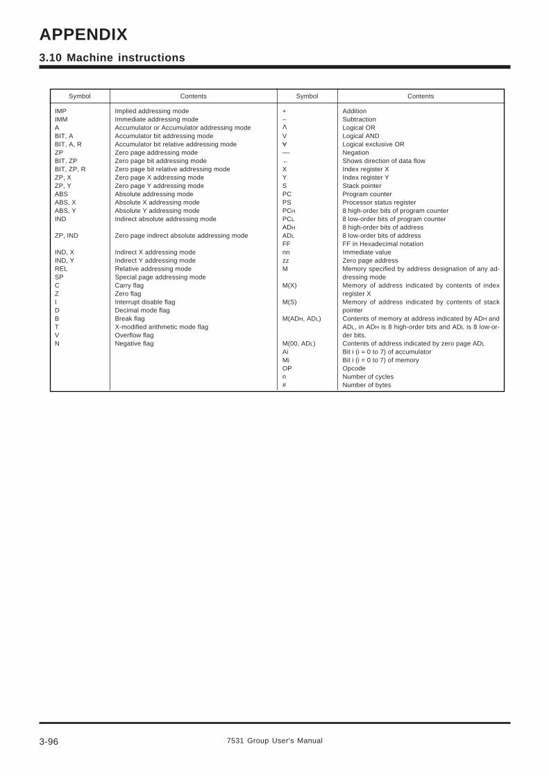
AdditionSubtractionLogical ORLogical ANDLogical exclusive ORNegationShows direction of data flowIndex register XIndex register YStack pointerProgram counterProcessor status register8 high-order bits of program counter8 low-order bits of program counter8 high-order bits of address8 low-order bits of addressFF in Hexadecimal notationImmediate valueZero page addressMemory specified by address designation of any ad-dressing modeMemory of address indicated by contents of indexregister XMemory of address indicated by contents of stackpointerContents of memory at address indicated by ADH andADL, in ADH is 8 high-order bits and ADL is 8 low-or-der bits.Contents of address indicated by zero page ADL
Bit i (i = 0 to 7) of accumulatorBit i (i = 0 to 7) of memoryOpcodeNumber of cyclesNumber of bytes
Implied addressing modeImmediate addressing modeAccumulator or Accumulator addressing modeAccumulator bit addressing modeAccumulator bit relative addressing modeZero page addressing modeZero page bit addressing modeZero page bit relative addressing modeZero page X addressing modeZero page Y addressing modeAbsolute addressing modeAbsolute X addressing modeAbsolute Y addressing modeIndirect absolute addressing mode
Zero page indirect absolute addressing mode
Indirect X addressing modeIndirect Y addressing modeRelative addressing modeSpecial page addressing modeCarry flagZero flagInterrupt disable flagDecimal mode flagBreak flagX-modified arithmetic mode flagOverflow flagNegative flag
IMPIMMABIT, ABIT, A, RZPBIT, ZPBIT, ZP, RZP, XZP, YABSABS, XABS, YIND
ZP, IND
IND, XIND, YRELSPCZIDBTVN
Symbol Contents Symbol Contents
+–
VV––←XYSPCPSPCH
PCL
ADH
ADL
FFnnzzM
M(X)
M(S)
M(ADH, ADL)
M(00, ADL)AiMiOPn#
V
3-96
APPENDIX
7531 Group User's Manual
3.10 Machine instructions
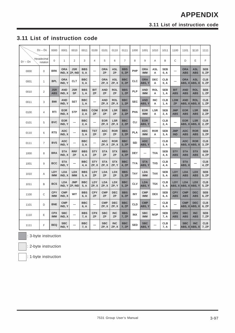
7531 Group User’s Manual 3-97
APPENDIX3.11 List of instruction code
3.11 List of instruction code
D7 – D4
D3 – D0
Hexadecimalnotation
0000
0001
0010
0011
0100
0101
0110
0111
1000
1001
1010
1011
1100
1101
1110
1111
0
1
2
3
4
5
6
7
8
9
A
B
C
D
E
F
0000
0
BRK
BPL
JSRABS
BMI
RTI
BVC
RTS
BVS
BRA
BCC
LDYIMM
BCS
CPYIMM
BNE
CPXIMM
BEQ
0001
1
ORAIND, X
ORAIND, Y
ANDIND, X
ANDIND, Y
EORIND, X
EORIND, Y
ADCIND, X
ADCIND, Y
STAIND, X
STAIND, Y
LDAIND, X
LDAIND, Y
CMPIND, X
CMPIND, Y
SBCIND, X
SBCIND, Y
0010
2
JSRZP, IND
CLT
JSRSP
SET
STP
—
—
—
RRFZP
—
LDXIMM
JMPZP, IND
WIT
—
—
—
0011
3
BBS0, A
BBC0, A
BBS1, A
BBC1, A
BBS2, A
BBC2, A
BBS3, A
BBC3, A
BBS4, A
BBC4, A
BBS5, A
BBC5, A
BBS6, A
BBC6, A
BBS7, A
BBC7, A
0100
4
—
—
BITZP
—
COMZP
—
TSTZP
—
STYZP
STYZP, X
LDYZP
LDYZP, X
CPYZP
—
CPXZP
—
0101
5
ORAZP
ORAZP, X
ANDZP
ANDZP, X
EORZP
EORZP, X
ADCZP
ADCZP, X
STAZP
STAZP, X
LDAZP
LDAZP, X
CMPZP
CMPZP, X
SBCZP
SBCZP, X
0110
6
ASLZP
ASLZP, X
ROLZP
ROLZP, X
LSRZP
LSRZP, X
RORZP
RORZP, X
STXZP
STXZP, Y
LDXZP
LDXZP, Y
DECZP
DECZP, X
INCZP
INCZP, X
0111
7
BBS0, ZP
BBC0, ZP
BBS1, ZP
BBC1, ZP
BBS2, ZP
BBC2, ZP
BBS3, ZP
BBC3, ZP
BBS4, ZP
BBC4, ZP
BBS5, ZP
BBC5, ZP
BBS6, ZP
BBC6, ZP
BBS7, ZP
BBC7, ZP
1000
8
PHP
CLC
PLP
SEC
PHA
CLI
PLA
SEI
DEY
TYA
TAY
CLV
INY
CLD
INX
SED
1001
9
ORAIMM
ORAABS, Y
ANDIMM
ANDABS, Y
EORIMM
EORABS, Y
ADCIMM
ADCABS, Y
—
STAABS, Y
LDAIMM
LDAABS, Y
CMPIMM
CMPABS, Y
SBCIMM
SBCABS, Y
1010
A
ASLA
DECA
ROLA
INCA
LSRA
—
RORA
—
TXA
TXS
TAX
TSX
DEX
—
NOP
—
1011
B
SEB0, A
CLB0, A
SEB1, A
CLB1, A
SEB2, A
CLB2, A
SEB3, A
CLB3, A
SEB4, A
CLB4, A
SEB5, A
CLB5, A
SEB6, A
CLB6, A
SEB7, A
CLB7, A
1100
C
—
—
BITABS
LDMZP
JMPABS
—
JMPIND
—
STYABS
—
LDYABS
LDYABS, X
CPYABS
—
CPXABS
—
1101
D
ORAABS
ORAABS, X
ANDABS
ANDABS, X
EORABS
EORABS, X
ADCABS
ADCABS, X
STAABS
STAABS, X
LDAABS
LDAABS, X
CMPABS
CMPABS, X
SBCABS
SBCABS, X
1110
E
ASLABS
ASLABS, X
ROLABS
ROLABS, X
LSRABS
LSRABS, X
RORABS
RORABS, X
STXABS
—
LDXABS
LDXABS, Y
DECABS
DECABS, X
INCABS
INCABS, X
1111
F
SEB0, ZP
CLB0, ZP
SEB1, ZP
CLB1, ZP
SEB2, ZP
CLB2, ZP
SEB3, ZP
CLB3, ZP
SEB4, ZP
CLB4, ZP
SEB5, ZP
CLB5, ZP
SEB6, ZP
CLB6, ZP
SEB7, ZP
CLB7, ZP
: 3-byte instruction
: 2-byte instruction
: 1-byte instruction
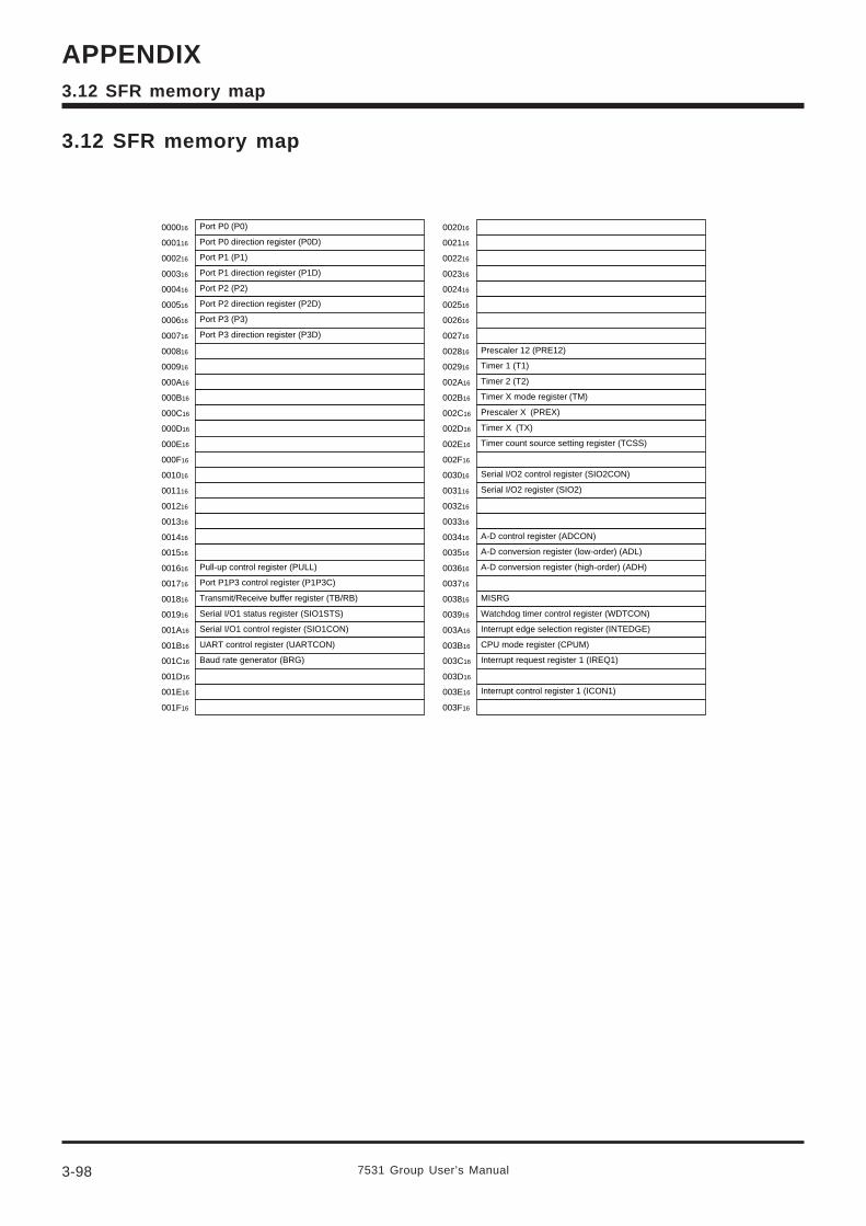
3-98
APPENDIX
7531 Group User’s Manual
3.12 SFR memory map
3.12 SFR memory map
000016
000116
000216
000316
000416
000516
000616
000716
000816
000916
000A16
000B16
000C16
000D16
000E16
000F16
001016
001116
001216
001316
001416
001516
001616
001716
001816
001916
001A16
001B16
001C16
001D16
001E16
001F16
Port P0 (P0)
Port P0 direction register (P0D)
Port P1 (P1)
Port P1 direction register (P1D)
Port P2 (P2)
Port P2 direction register (P2D)
Port P3 (P3)
Port P3 direction register (P3D)
Pull-up control register (PULL)
Transmit/Receive buffer register (TB/RB)
Serial I/O1 status register (SIO1STS)
Serial I/O1 control register (SIO1CON)
UART control register (UARTCON)
Baud rate generator (BRG)
Port P1P3 control register (P1P3C)
002016
002116
002216
002316
002416
002516
002616
002716
002816
002916
002A16
002B16
002C16
002D16
002E16
002F16
003016
003116
003216
003316
003416
003516
003616
003716
003816
003916
003A16
003B16
003C16
003D16
003E16
003F16
Timer count source setting register (TCSS)
A-D conversion register (low-order) (ADL)
Prescaler 12 (PRE12)
Timer 1 (T1)
Timer 2 (T2)
Timer X mode register (TM)
Prescaler X (PREX)
Timer X (TX)
Serial I/O2 control register (SIO2CON)
Serial I/O2 register (SIO2)
A-D control register (ADCON)
A-D conversion register (high-order) (ADH)
MISRG
Watchdog timer control register (WDTCON)
Interrupt edge selection register (INTEDGE)
CPU mode register (CPUM)
Interrupt request register 1 (IREQ1)
Interrupt control register 1 (ICON1)
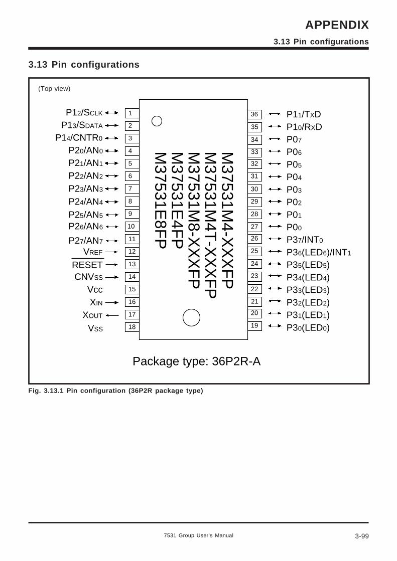
7531 Group User’s Manual 3-99
APPENDIX3.13 Pin configurations
3.13 Pin configurations
Fig. 3.13.1 Pin configuration (36P2R package type)
(Top view)
Package type: 36P2R-A
10
1
2
3
4
6
7
8
9
11
12
14
15
16
5
13
17
18
36
35
34
33
31
30
26
25
24
23
22
21
20
19
32
27
29
28
P00
CNVSS
XOUT
XIN
VSS
P01
P02
P03
P04
P30(LED0)
Vcc
VREF
P05
P10/RXD
P26/AN6
P27/AN7
P11/TXDP12/SCLK
P13/SDATA
P23/AN3
P22/AN2
P21/AN1
P20/AN0
P31(LED1)
P36(LED6)/INT1
P24/AN4
P25/AN5
P06
P07
P37/INT0
RESET
M37531M
4-XX
XF
PM
37531M4T
-XX
XF
PM
37531M8-X
XX
FP
M37531E
4FP
M37531E
8FP
P14/CNTR0
P35(LED5)P34(LED4)P33(LED3)P32(LED2)
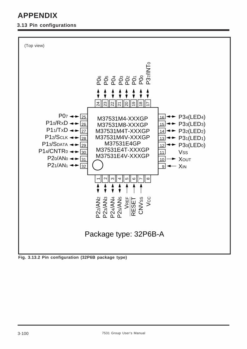
3-100
APPENDIX
7531 Group User’s Manual
Fig. 3.13.2 Pin configuration (32P6B package type)
(Top view)
Package type: 32P6B-A
P07
P10/RXDP11/TXDP12/SCLK
P13/SDATA
P14/CNTR0
P20/AN0
P21/AN1 32
31
30
29
28
27
26
25 P34(LED4)P33(LED3)P32(LED2)P31(LED1)P30(LED0)VSS
XOUT
XIN9
10
11
12
13
14
15
16
2 876531 4
VC
C
CN
VS
S
RE
SE
T
P22
/AN
2
P05
20 1718192124
P02
P04
P03
P06
23 22
P01
P00
P37
/INT
0
M37531M4-XXXGPM37531M8-XXXGP
M37531M4T-XXXGPM37531M4V-XXXGP
M37531E4GPM37531E4T-XXXGPM37531E4V-XXXGP
P23
/AN
3
P24
/AN
4
P25
/AN
5
VR
EF
3.13 Pin configurations
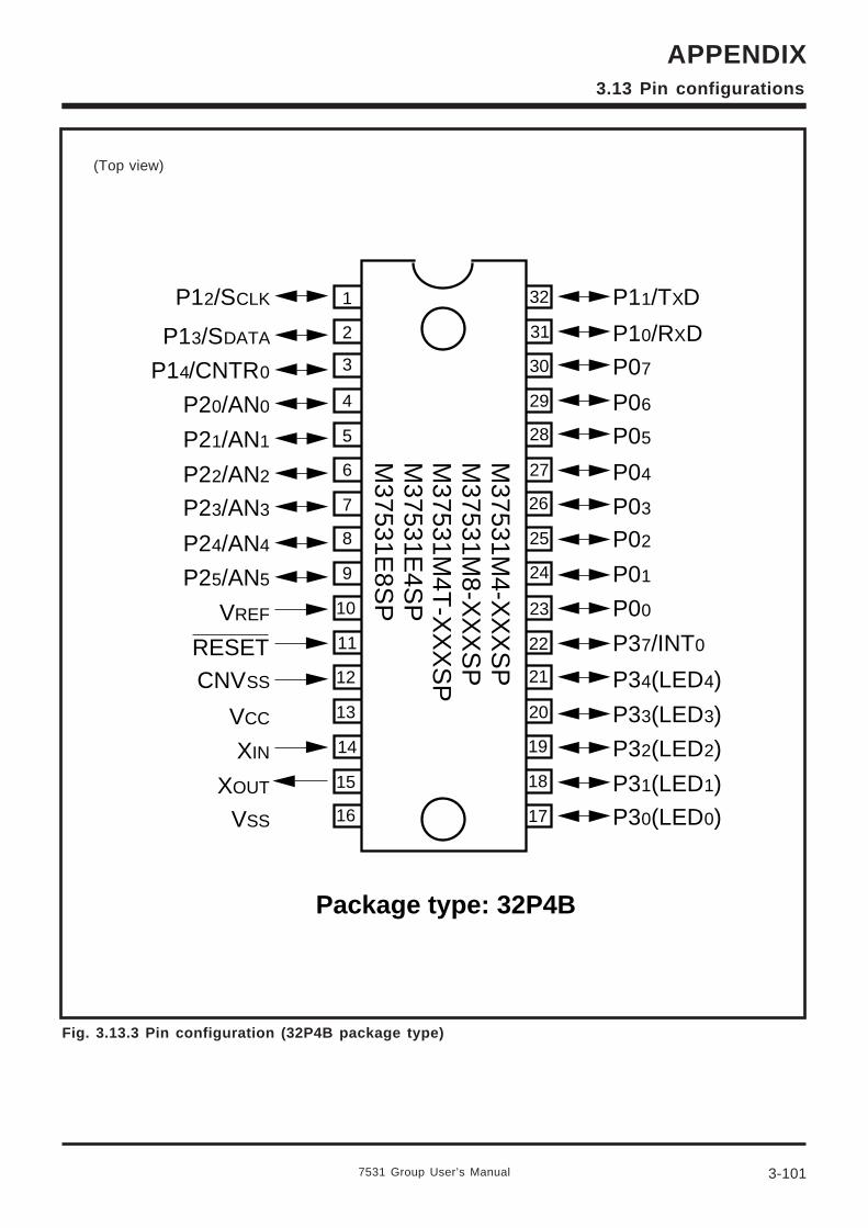
7531 Group User’s Manual 3-101
APPENDIX3.13 Pin configurations
Fig. 3.13.3 Pin configuration (32P4B package type)
(Top view)
1
2
3
4
5
6
7
8
9
10
11
12
13
14
15
16
CNVSS
P12/SCLK
P13/SDATA
P14/CNTR0
P20/AN0
P21/AN1
P22/AN2
P23/AN3
P24/AN4
VCC
XIN
XOUT
VSS
P11/TXD
P10/RXD
P07
P06
P05
P04
P30(LED0)
P25/AN5
VREF
RESET
P00
P33(LED3)
P32(LED2)
P31(LED1)
M37531M
4-XX
XS
PM
37531M8-X
XX
SP
M37531M
4T-X
XX
SP
M37531E
4SP
M37531E
8SP
32
P01
P02
P03
14
15
16
P37/INT0
P34(LED4)
17
18
19
20
21
22
23
24
25
26
27
28
29
30
31
Package type: 32P4B
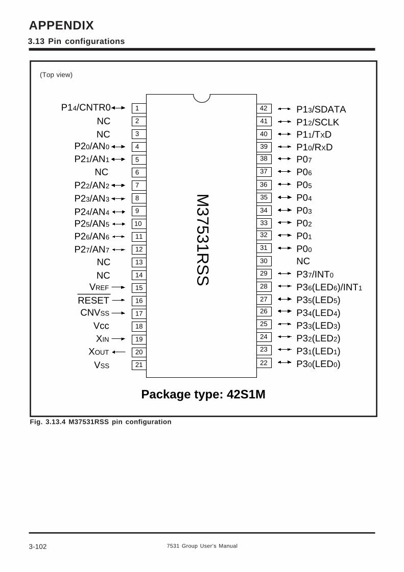
3-102
APPENDIX
7531 Group User’s Manual
Fig. 3.13.4 M37531RSS pin configuration
(Top view)
3.13 Pin configurations
10
1
2
3
4
6
7
8
9
11
12
14
15
16
5
13
17
18
36
35
34
33
31
30
26
25
24
23
22
32
27
29
28
19
20
21
42
41
40
39
37
38
P00
CNVSS
XOUT
XIN
VSS
P01
P02
P03
P04
P30(LED0)
Vcc
VREF
P05
P12/SCLK
P25/AN5
P26/AN6
P13/SDATAP14/CNTR0
NC
P22/AN2
NCP21/AN1
P20/AN0
P31(LED1)
P36(LED6)/INT1
P23/AN3
P24/AN4
P06
P07
P37/INT0
RESET
M37531R
SS
NC
P35(LED5)P34(LED4)P33(LED3)P32(LED2)
NC
P10/RXDP11/TXD
NCNC
P27/AN7
Package type: 42S1M

MITSUBISHI SEMICONDUCTORSUSER’S MANUAL7531 Group
Jul. First Edition 1998, Sep. Second Edition 1999
Editioned byCommittee of editing of Mitsubishi Semiconductor USER’S MANUAL
Published byMitsubishi Electric Corp., Semiconductor Marketing Division
This book, or parts thereof, may not be reproduced in any form without permissionof Mitsubishi Electric Corporation.
©1999 MITSUBISHI ELECTRIC CORPORATION

MITSUBISHI ELECTRIC CORPORATIONHEAD OFFICE: 2-2-3, MARUNOUCHI, CHIYODA-KU, TOKYO 100-8310, JAPAN
User’s Manual7531 Group
© 1999 MITSUBISHI ELECTRIC CORPORATION.New publication, effective Sep. 1999.
Specifications subject to change without notice.


