Page 1
8/7/2019 8-bit Cirrent Steering DAC
http://slidepdf.com/reader/full/8-bit-cirrent-steering-dac 1/21
1
8 Bit Current Steering DAC
Taoufiq Bellamine
I. Abstract
In this paper, we will go through the analysis, design and simulation of an 8-Bit Current Steering
DAC operating from three supplies of 5v, 2.5v and 3.5v. The 8-bit binary input ranges from 0 − 5v,
and the clock can be as high as 25MHz. The common-mode voltage V cm runs from a 3.5v rail, and
the positive input of the Op Amp from a V ref = 2.5v reference. The process used for this purpose is a
0.5µm AMI C5N CMOS process. The fact that the current steering topology is used instead of the R2R
topology made it more challenging to achieve good INL as well as DNL results. Major glitching issues
were encountered during the design step because of the coupling effect of the clock as well as the digital
inputs to the output through parasitic capacitances, but these issues were overcome through the use of
digital latches as well as charge injection switches. An overall swing of 2.06v was achieved along with
an SNDR of 30dB and an LSB step of 8.3mv. Worthwhile to note also, is that the DAC cannot drive
resistive loads of values less than 100K Ω.
Page 2
8/7/2019 8-bit Cirrent Steering DAC
http://slidepdf.com/reader/full/8-bit-cirrent-steering-dac 2/21
Page 3
8/7/2019 8-bit Cirrent Steering DAC
http://slidepdf.com/reader/full/8-bit-cirrent-steering-dac 3/21
3
VI Testing and Improvements 19
VI-A Power Dissipation . . . . . . . . . . . . . . . . . . . . . . . . . . . . . . . . . . . . 19
VI-B Testing . . . . . . . . . . . . . . . . . . . . . . . . . . . . . . . . . . . . . . . . . . 19
VII Conclusion and Improvements 20
VII-A Conclusion . . . . . . . . . . . . . . . . . . . . . . . . . . . . . . . . . . . . . . . . 20
VII-B Improvements . . . . . . . . . . . . . . . . . . . . . . . . . . . . . . . . . . . . . . 20
VIII Biography 21
LIST OF FIGURES
1 Top Level Block Diagram of the DAC . . . . . . . . . . . . . . . . . . . . . . . . . . . . . . 5
2 Unit Current Cell . . . . . . . . . . . . . . . . . . . . . . . . . . . . . . . . . . . . . . . . . 6
3 Binary Current Cell Array . . . . . . . . . . . . . . . . . . . . . . . . . . . . . . . . . . . . 7
4 Gated-D latch . . . . . . . . . . . . . . . . . . . . . . . . . . . . . . . . . . . . . . . . . . . 8
5 Gated D latch outputs . . . . . . . . . . . . . . . . . . . . . . . . . . . . . . . . . . . . . . . 9
6 Differential Pair . . . . . . . . . . . . . . . . . . . . . . . . . . . . . . . . . . . . . . . . . . 10
7 Gain Stage . . . . . . . . . . . . . . . . . . . . . . . . . . . . . . . . . . . . . . . . . . . . . 11
8 Gain/Phase Op Amp plot . . . . . . . . . . . . . . . . . . . . . . . . . . . . . . . . . . . . . 11
9 Complete DAC schematic . . . . . . . . . . . . . . . . . . . . . . . . . . . . . . . . . . . . . 12
10 Ramp DAC Output . . . . . . . . . . . . . . . . . . . . . . . . . . . . . . . . . . . . . . . . 13
11 Zoomed-in version of ramping output . . . . . . . . . . . . . . . . . . . . . . . . . . . . . . 13
12 Error signal . . . . . . . . . . . . . . . . . . . . . . . . . . . . . . . . . . . . . . . . . . . . 14
13 Reconstructed Sine Wave . . . . . . . . . . . . . . . . . . . . . . . . . . . . . . . . . . . . . 14
14 DFT of the output . . . . . . . . . . . . . . . . . . . . . . . . . . . . . . . . . . . . . . . . . 15
15 The current cells array layout . . . . . . . . . . . . . . . . . . . . . . . . . . . . . . . . . . . 15
16 The unit cell differential switch layout . . . . . . . . . . . . . . . . . . . . . . . . . . . . . . 16
17 The latch layout . . . . . . . . . . . . . . . . . . . . . . . . . . . . . . . . . . . . . . . . . . 16
18 The Op Amp layout . . . . . . . . . . . . . . . . . . . . . . . . . . . . . . . . . . . . . . . . 17
19 The overall layout of the chip . . . . . . . . . . . . . . . . . . . . . . . . . . . . . . . . . . 18
Page 4
8/7/2019 8-bit Cirrent Steering DAC
http://slidepdf.com/reader/full/8-bit-cirrent-steering-dac 4/21
4
II . Introduction
A. DAC Architectures
DACs are the interface between the analog and digital worlds in electrical engineering. The progress
achieved during the last decade in computing and data processing is closely related to these chips. Four
major DAC topologies can be distinguished:
• Binary Weighted DACs: These DACs consist of either current sources or resistors for each bit.
These elements are connected to a summing point which provides the output.
• R2R Ladder DACs: These DACs consist of a structure of resistor values which can be closely
matched. This topology is binary weighted and can provide a higher resolution compared to its
purely binary weighted counterpart.
• Delta-Sigma DACs: These DACs are relatively new and they rely on pulse density and noise shaping
techniques which allow for the use of a lower resolution DAC in the forward path (usually 1 bit).
• Segmented DACs: These DACs are a hybrid between the binary weighted and the thermometer
decoded topologies. This mix proved to be the fastest and most precise topology, at the expense of
die area.
B. Project Objectives
The major objective for this project was to build an 8-bit current steering Digital to Analog Convertor.
The table I below provides the project’s specifications:
Supplies Vdd=5v Vcm=3.5v Vref=2.5v
Clock F requency Up to 25 MHz
InputF requency Up to 10 MHz
Drive At least 100 K Ω
Topology Binary Weighted
TABLE I
DAC Specifications
Page 5
8/7/2019 8-bit Cirrent Steering DAC
http://slidepdf.com/reader/full/8-bit-cirrent-steering-dac 5/21
Page 6
8/7/2019 8-bit Cirrent Steering DAC
http://slidepdf.com/reader/full/8-bit-cirrent-steering-dac 6/21
6
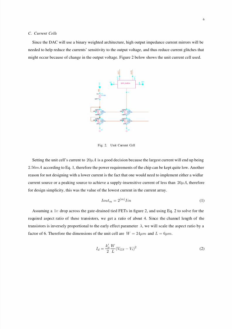
C. Current Cells
Since the DAC will use a binary weighted architecture, high output impedance current mirrors will be
needed to help reduce the currents’ sensitivity to the output voltage, and thus reduce current glitches that
might occur because of change in the output voltage. Figure 2 below shows the unit current cell used.
Fig. 2. Unit Current Cell
Setting the unit cell’s current to 20µA is a good decision because the largest current will end up being
2.56mA according to Eq. 1, therefore the power requirements of the chip can be kept quite low. Another
reason for not designing with a lower current is the fact that one would need to implement either a widlar
current source or a peaking source to achieve a supply-insensitive current of less than 20µA, therefore
for design simplicity, this was the value of the lowest current in the current array.
Ioutm = 2(m)Iin (1)
Assuming a 1v drop across the gate-drained tied FETs in figure 2, and using Eq. 2 to solve for the
required aspect ratio of these transistors, we get a ratio of about 4. Since the channel length of the
transistors is inversely proportional to the early effect parameter λ, we will scale the aspect ratio by a
factor of 6. Therefore the dimensions of the unit cell are W = 24µm and L = 6µm.
I d =k
n
2
W
L(V GS − V t)
2 (2)
Page 7
8/7/2019 8-bit Cirrent Steering DAC
http://slidepdf.com/reader/full/8-bit-cirrent-steering-dac 7/21
7
All other current cells are a factor of 2m greater than the original unit cell, where m is the bit number.
The following figure show the whole binary weighted current cell array. The MSB has the following
dimensions W = 3024µm and L = 6µm and runs a 2.56mA current.
Fig. 3. Binary Current Cell Array
D. Differential Switches
The differential switches are designed so that the voltage drop across the switches when they are on
is the same for all transistors. Since the current scales up by a factor of 2, the Ron resistances will need
to be scaled down by the same factor. The resistance of the Unit Cell was determined based on Eq. 3.
Ron =1
K nW L
(V GS − V TN )(3)
The transconductance value used is K n = 108µA/V 2 (according to the parameter sheet for this process)
and using the minimal estimate of the gate-source voltage (V GS ) predicted by Eq. 4, one can set the Ron
in Eq. 3 to 100Ω and solve for the aspect ratio of the switch while assuming a minimal channel length
of 600nm (to keep the resistance small). By doing so, we get the following dimensions W = 18µm and
L = 600nm. This aspect ratio will have to be scaled up by a factor of 2 progressively as mentioned
earlier.
V GSmin = V dd − 2V ov − V TN (4)
Page 8
8/7/2019 8-bit Cirrent Steering DAC
http://slidepdf.com/reader/full/8-bit-cirrent-steering-dac 8/21
8
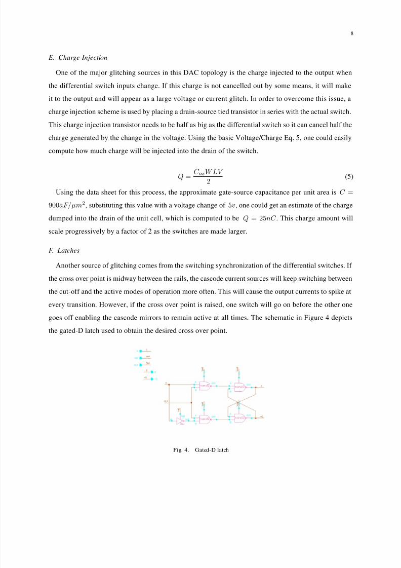
E. Charge Injection
One of the major glitching sources in this DAC topology is the charge injected to the output when
the differential switch inputs change. If this charge is not cancelled out by some means, it will make
it to the output and will appear as a large voltage or current glitch. In order to overcome this issue, a
charge injection scheme is used by placing a drain-source tied transistor in series with the actual switch.
This charge injection transistor needs to be half as big as the differential switch so it can cancel half the
charge generated by the change in the voltage. Using the basic Voltage/Charge Eq. 5, one could easily
compute how much charge will be injected into the drain of the switch.
Q =C oxWLV
2(5)
Using the data sheet for this process, the approximate gate-source capacitance per unit area is C =
900aF/µm2, substituting this value with a voltage change of 5v, one could get an estimate of the charge
dumped into the drain of the unit cell, which is computed to be Q = 25nC . This charge amount will
scale progressively by a factor of 2 as the switches are made larger.
F. Latches
Another source of glitching comes from the switching synchronization of the differential switches. If
the cross over point is midway between the rails, the cascode current sources will keep switching between
the cut-off and the active modes of operation more often. This will cause the output currents to spike at
every transition. However, if the cross over point is raised, one switch will go on before the other one
goes off enabling the cascode mirrors to remain active at all times. The schematic in Figure 4 depicts
the gated-D latch used to obtain the desired cross over point.
Fig. 4. Gated-D latch
Page 9
8/7/2019 8-bit Cirrent Steering DAC
http://slidepdf.com/reader/full/8-bit-cirrent-steering-dac 9/21
9
Simulation of the latch outputs (Q and Q) produces figure 5. The cross over point is 3.83v as shown
below:
Fig. 5. Gated D latch outputs
G. Op Amp
1) Input Stage: The input stage of the Op Amp is a standard differential pair with a cascoded tail
source to improve the CMRR. It can be seen from Eq. 6 that the higher the rtail the lower the CM gain,
and therefore the higher the CMRR is.
CM =1
2gm(mir)rtail(6)
The resistive bias circuitry is set to run a 100µA tail current in the differential pair. Keeping the tail
current low is preferred since the gain is inversely proportional to the square root of the current. Eq. 7
is an expression for the open loop gain of this stage.
DM −gm(dp)(ro(mir)//ro(dp)) (7)
Page 10
8/7/2019 8-bit Cirrent Steering DAC
http://slidepdf.com/reader/full/8-bit-cirrent-steering-dac 10/21
10
The figure below shows the differential stage of the Op Amp.
Fig. 6. Differential Pair
Solving for the small signal parameters for this differential pair, we get the values listed in Table II:
Parameter Expression Value
gm(dp)
q 2I dK n
W
L1.8mA/V
gm(mir)
q 2I dK p
W L
824.5µA/V
ro(mir)1
λp Id250K Ω
ro(dp) 1λn Id
200K Ω
TABLE II
Differential pair small signal parameters
Substituting the values in Table II into Eq. 7 (page 9) gives a differential gain of about −200v/v.
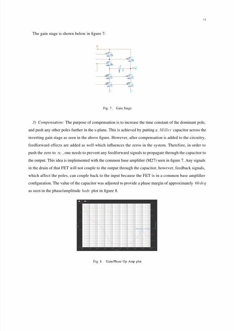
2) Gain Stage: The gain stage for this Op Amp is a basic common source amplifier, and its gain
is given by Eq.8. Since the gain stage is running a 50µA current, the transconductance of the PMOS
(gm(cs)) is the same as gm(mir) of the differential stage, and the output impedance of this stage (ro(cs))
is the same as ro(mir). Substituting these values into 8, gives a gain of about −206v/v. Therefore the
overall gain of the Op Amp is 93dB.
Acs −gm(cs)(ro(cs)//ro(tail)) −gm(cs)ro(cs) (8)
Page 11
8/7/2019 8-bit Cirrent Steering DAC
http://slidepdf.com/reader/full/8-bit-cirrent-steering-dac 11/21
11
The gain stage is shown below in figure 7:
Fig. 7. Gain Stage
3) Compensation: The purpose of compensation is to increase the time constant of the dominant pole,
and push any other poles further in the s-plane. This is achieved by putting a Miller capacitor across the
inverting gain stage as seen in the above figure. However, after compensation is added to the circuitry,
feedforward effects are added as well which influences the zeros in the system. Therefore, in order to
push the zero to ∞ , one needs to prevent any feedforward signals to propagate through the capacitor to
the output. This idea is implemented with the common base amplifier (M27) seen in figure 7. Any signals
in the drain of that FET will not couple to the output through the capacitor, however, feedback signals,
which affect the poles, can couple back to the input because the FET is in a common base amplifier
configuration. The value of the capacitor was adjusted to provide a phase margin of approximately 60deg
as seen in the phase/amplitude bode plot in figure 8.
Fig. 8. Gain/Phase Op Amp plot
Page 12
8/7/2019 8-bit Cirrent Steering DAC
http://slidepdf.com/reader/full/8-bit-cirrent-steering-dac 12/21
12
4) Op Amp results: The Op Amp characteristics are summarized in Table III below. It is also worth-
while to mention that the Op Amp is used as an active lowpass filter with a cutoff frequency of 2.65MHz.
Av 92dB
F t 40MHz
F cutoff 2.6MHz
TABLE III
Op Amp results
IV.Simulation
A. Overall Schematic
The DAC’s overall schematic is shown below in figure 9. Each component was discussed in detail in
previous sections.
Fig. 9. Complete DAC schematic
The independant sources on the top of the schematic are V cm, V dd and V clk. The 8 blocks on the left
are the latches, whereas the big block on the right is the current cells’ array. The output is simulated witha 5M Ω resistor and a 20pF capacitor to represent the oscilloscope’s impedance. Two kinds of digital
inputs were used; Standard ramping inputs, and sine wave inputs. The results for both simulations will
be outlined shortly.
Page 13
8/7/2019 8-bit Cirrent Steering DAC
http://slidepdf.com/reader/full/8-bit-cirrent-steering-dac 13/21
13
B. Simulation Results
1) Ramp Inputs: Simulating the DAC with a digital ramp produces the output in figure 10. It is to
be noted that the clock frequency used for this simulation is F clk = 10MHz and the inputs change at a
rate of F in = 2MHz.
Fig. 10. Ramp DAC Output
A zoomed-in version of figure 10 is shown below:
Fig. 11. Zoomed-in version of ramping output
Figure 11 above shows that the step of the DAC is about 8.3mv. This step was achieved based on
the desired amount of swing. One can use Eq. 9 below to solve for the LSB, and therefore the resistors
which convert the DAC’s current to a proportional voltage can be adjusted to achieve that LSB (assumingthe unit cell current has already been set to 20µA).
LSB =V swing
2M (9)
Page 14
8/7/2019 8-bit Cirrent Steering DAC
http://slidepdf.com/reader/full/8-bit-cirrent-steering-dac 14/21
14
An error graph can be generated by comparing the ramping output of the DAC to an ideal ramp. The
integrated-non-linearity (INL), which is a measure of how much the DAC transfer characteristic differs
from the ideal characteristic, can be extracted from this graph (INL 1LSB).The error signal is shown
in figure 12 below:
Fig. 12. Error signal
2) Sine wave inputs: A Matlab script was used to generate samples from a 20KHz sine wave. The
sine wave samples were then exported to the Cadence design tools, and a top-level simulation was run.
The output is shown in figure 13 below:
Fig. 13. Reconstructed Sine Wave
Page 15
8/7/2019 8-bit Cirrent Steering DAC
http://slidepdf.com/reader/full/8-bit-cirrent-steering-dac 15/21
15
Running a discrete Fourier transform on the result discussed earlier enables us to find the signal-to-
noise-distortion-ratio (SNDR) by substracting the highest distorted tone from the dominant 20KHz tone.
The SNDR is evaluated to be approximately 30dB, which is a reasonable value for an 8-bit resolution.
Fig. 14. DFT of the output
V. Layout
Layout was a straightforward procedure. However, some issues were encountered during the layout of
several blocks, but most of the errors were promptly detected and fixed. Parasitic extraction of the charge
injection switches was not completed because LV S does not recognize drain-source tied transistors as
regular FETs, therefore the only fix for this issue was to ignore these switches during the LV S check.
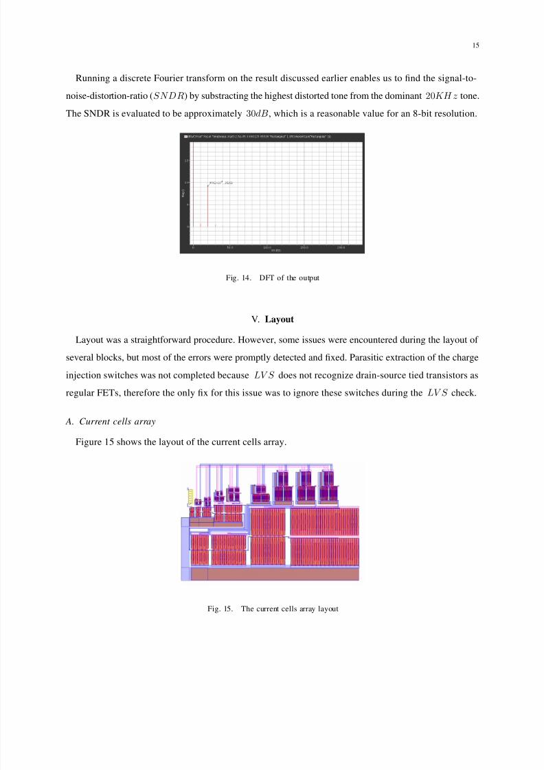
A. Current cells array
Figure 15 shows the layout of the current cells array.
Fig. 15. The current cells array layout
Page 16
8/7/2019 8-bit Cirrent Steering DAC
http://slidepdf.com/reader/full/8-bit-cirrent-steering-dac 16/21
16
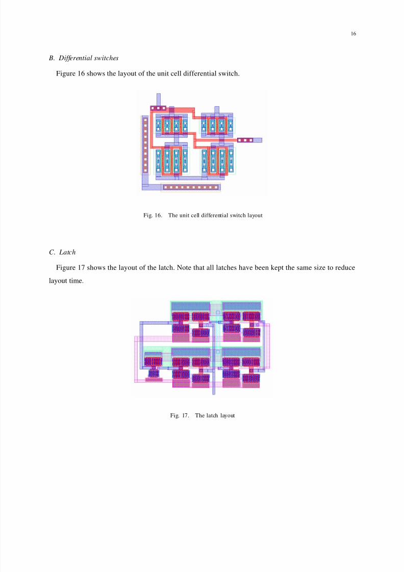
B. Differential switches
Figure 16 shows the layout of the unit cell differential switch.
Fig. 16. The unit cell differential switch layout
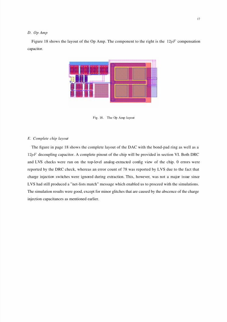
C. Latch
Figure 17 shows the layout of the latch. Note that all latches have been kept the same size to reduce
layout time.
Fig. 17. The latch layout
Page 17
8/7/2019 8-bit Cirrent Steering DAC
http://slidepdf.com/reader/full/8-bit-cirrent-steering-dac 17/21
17
D. Op Amp
Figure 18 shows the layout of the Op Amp. The component to the right is the 12pF compensation
capacitor.
Fig. 18. The Op Amp layout
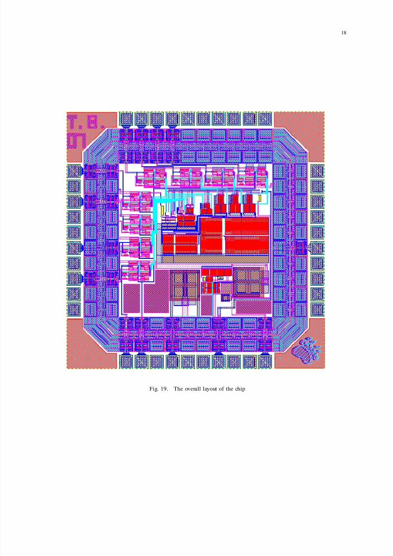
E. Complete chip layout
The figure in page 18 shows the complete layout of the DAC with the bond-pad ring as well as a
12pF decoupling capacitor. A complete pinout of the chip will be provided in section VI. Both DRC
and LVS checks were run on the top-level analog-extracted config view of the chip. 0 errors were
reported by the DRC check, whereas an error count of 78 was reported by LVS due to the fact that
charge injection switches were ignored during extraction. This, however, was not a major issue since
LVS had still produced a ”net-lists match” message which enabled us to proceed with the simulations.
The simulation results were good, except for minor glitches that are caused by the abscence of the charge
injection capacitances as mentioned earlier.
Page 18
8/7/2019 8-bit Cirrent Steering DAC
http://slidepdf.com/reader/full/8-bit-cirrent-steering-dac 18/21
18
Fig. 19. The overall layout of the chip
Page 19
8/7/2019 8-bit Cirrent Steering DAC
http://slidepdf.com/reader/full/8-bit-cirrent-steering-dac 19/21
19
VI . Testing and Improvements
A. Power Dissipation
The portion of the chip which consumes the most power is the current cells array because of its binary
nature. Table IV is a listing of the major areas where most of the static power is consumed in the actual
chip.
CurrentArray 17.85mW
OpAmp 1.25mW
TABLE IV
Static Power Results
B. Testing
Out of the 40 pins available, only 14 pins are being used. Table V below shows the pinout for the
chip (the binary inputs are labeled from B0 to B7). All other pins in the chip are padded as No-Connects
(NC).
P in# Function Pin# Function
12 B7 23 B1
13 B6 26 B0
14 B5 27 CLK
15 B4 29 VREF
16 B3 32 VCM
18 B2 35 VOUT
21 VDD 40 GND
TABLE V
DAC Pinout
Page 20
8/7/2019 8-bit Cirrent Steering DAC
http://slidepdf.com/reader/full/8-bit-cirrent-steering-dac 20/21
20
A simple procedure can be outlined in order to test the DAC, and it goes as follows:
• Connect all necessary rails using Table V as a reference.
• Connect the binary inputs to a binary ramp with a frequency of 2 MHz, and a range of 0-5v.
• Connect the output to the scope and remember not to place a load less than 100 K Ω. A lowpass
filter can also be applied at the output to smooth the signal.
• Observe the power consumption from the supplies and make sure it does not go above 20mW from
all supplies combined. If it does, it is indicative of a short connection.
VII. CONCLUSION AND IMPROVEMENTS
A. Conclusion
Using the AMI 0.5µm process, an 8-bit current steering DAC was appropriately built. Both schematic
and parasitic simulation results proved appropriate operation of the DAC, with a minor pseudo-glitching
issue in the parasitic results caused by the LVS check not extracting the charge injection capacitances
appropriately. This design can be used in any applications requiring a moderate speed and an 8-bit
resolution.
B. Improvements
Many improvements could be implemented for this design to increase the speed and the swing as well
as to reduce the glitch-power:• High Swing Current Scheme: A high swing mirror could be used to improve the output swing by
getting rid of the threshold term (V T ) in the minimal achievable voltage.
• Matching Layout Techniques: Matching techniques could also be used to improve glitch-power
rejection.
• Transimpedance Amplifier: A transimpedance amplifier could be used to sum the currents from
the current array instead of using resistors. This would reduce temperature dependencies and provide
more accurate results.
• Temperature Independant Biasing: More elaborate biasing circuitry could be incorporated into
this design to minimize both temperature and power supply dependencies.
• Higher Resolution: Higher resolution using a segmented topology could be implemented for high
speed/resolution applications.
Page 21
8/7/2019 8-bit Cirrent Steering DAC
http://slidepdf.com/reader/full/8-bit-cirrent-steering-dac 21/21
21
VIII. BIOGRAPHY
Taoufiq Bellamine was born in Rabat, Morocco. He graduated from My. Taib Alalaoui high school
in Sale, Morocco. He is currently a fifth-year student at the University of Maine, studying towards two
degrees in Electrical and Computer Engineering and will be graduating in May 2007. He speaks fluent
French, Arabic and English, as well as his parents’ native dialect (Berber). He has received numerous
honors and scholarships while at the University of Maine, and had also acquired industry experience at
Allegro Microsystems during Summer 06. His interests are circuit design (Analog and Digital) as well
as programming.