Page 1
#8 : Memory Hierarchy
Computer Architecture 2019/2020
Ricardo RochaRicardo RochaComputer Science Department, Faculty of Sciences, University of Porto
Slides based on the book
‘Computer Organization and Design, The Hardware/Software Interface, 5th Edition
David Patterson and John Hennessy, Morgan Kaufmann’
Sections 5.1 – 5.5 and 5.7
Page 2
Memory Hierarchy
“Ideally one would desire an indefinitely large memory capacity such that
any particular […] word would be immediately available. […] We are […]
forced to recognize the possibility of constructing a hierarchy of memories,
each of which has greater capacity than the preceding but which is less
quickly accessible.”
1#8 : Memory HierarchyComputer Architecture 2019/2020
quickly accessible.”
A. W. Burks, H. H. Goldstine, and J. von Neumann. Preliminary Discussion
of the Logical Design of an Electronic Computing Instrument, 1946.
Page 3
Memory Hierarchy
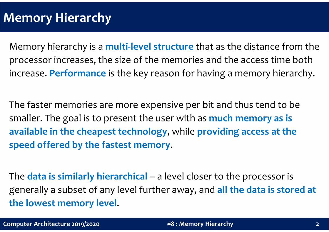
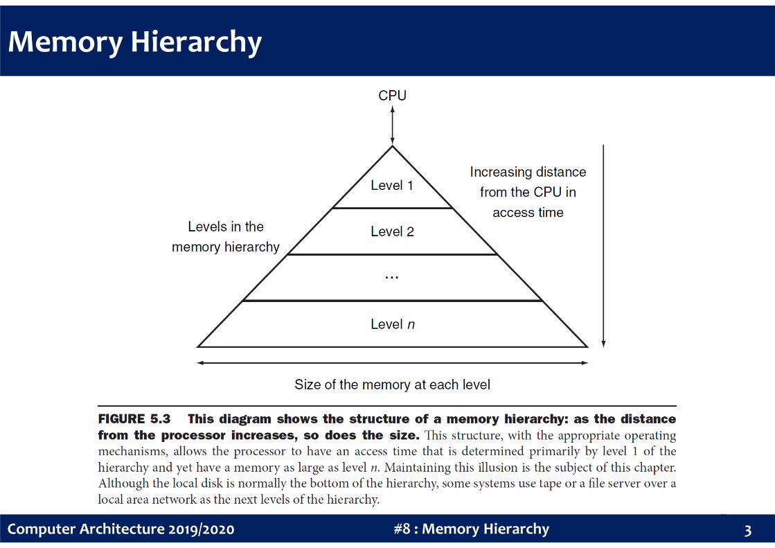
Memory hierarchy is a multi-level structure that as the distance from the
processor increases, the size of the memories and the access time both
increase. Performance is the key reason for having a memory hierarchy.
The faster memories are more expensive per bit and thus tend to be
smaller. The goal is to present the user with as much memory as is
2#8 : Memory HierarchyComputer Architecture 2019/2020
smaller. The goal is to present the user with as much memory as is
available in the cheapest technology, while providing access at the
speed offered by the fastest memory.
The data is similarly hierarchical – a level closer to the processor is
generally a subset of any level further away, and all the data is stored at
the lowest memory level.
Page 4
Memory Hierarchy
3#8 : Memory HierarchyComputer Architecture 2019/2020
Page 5
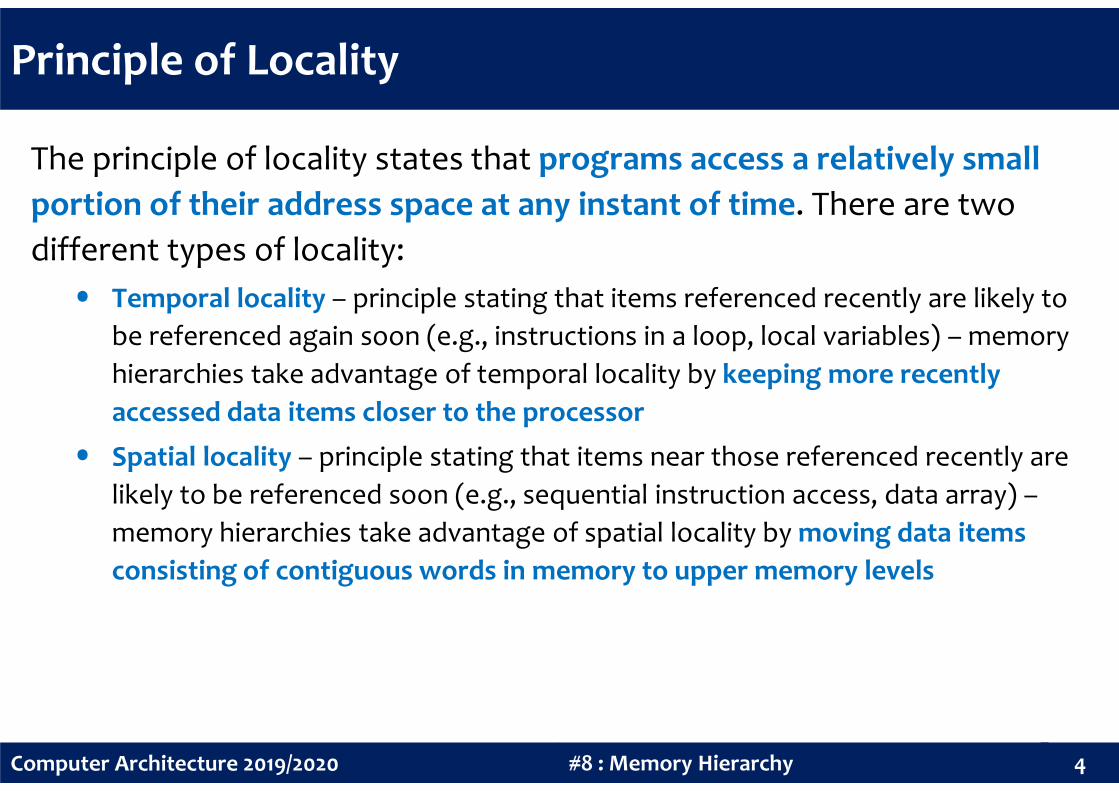
Principle of Locality
The principle of locality states that programs access a relatively small
portion of their address space at any instant of time. There are two
different types of locality:
• Temporal locality – principle stating that items referenced recently are likely to
be referenced again soon (e.g., instructions in a loop, local variables) – memory
hierarchies take advantage of temporal locality by keeping more recently
accessed data items closer to the processor
4#8 : Memory HierarchyComputer Architecture 2019/2020
accessed data items closer to the processor
• Spatial locality – principle stating that items near those referenced recently are
likely to be referenced soon (e.g., sequential instruction access, data array) –
memory hierarchies take advantage of spatial locality by moving data items
consisting of contiguous words in memory to upper memory levels
Page 6
Data is copied between only two adjacent levels at a time. Within each
level, the minimal unit of data is called a block (or line).
Hits and Misses
5#8 : Memory HierarchyComputer Architecture 2019/2020
Page 7
Hits and Misses
If the data requested by the processor appears in some block in the
upper memory level, this is called a hit. Otherwise, the request is called a
miss and the next memory level is then accessed to retrieve the block
containing the requested data.
6#8 : Memory HierarchyComputer Architecture 2019/2020
The hit rate is the fraction of memory accesses found in the upper
memory level – often used as a measure of the performance of the
memory hierarchy. The miss rate (1−hit rate) is the fraction of memory
accesses not found in the upper memory level.
Page 8
Hits and Misses
Hit time is the time to access the upper memory level, which includes
the time needed to determine whether the access is a hit or a miss.
Miss penalty is the time to replace a block in the upper memory level
with the corresponding block from the next memory level, plus the time
to deliver this block to the processor. The time to access the next
7#8 : Memory HierarchyComputer Architecture 2019/2020
to deliver this block to the processor. The time to access the next
memory level is the major component of the miss penalty.
If the hit rate is high enough, the memory hierarchy has an effective
access time close to that of the upper memory level and therefore be
able to virtually represent a size equal to that of the lowest memory
level.
Page 9
Memory Technologies
8#8 : Memory HierarchyComputer Architecture 2019/2020
Page 10
Cache Memory
Cache: a safe place for hiding or storing things.
Webster’s New World Dictionary of the American Language, 1988.
Cache memory is the level of the memory hierarchy closest to the CPU.
9#8 : Memory HierarchyComputer Architecture 2019/2020
Caches first appeared in research computers in the early 1960s and in
production computers later in that same decade. Every general purpose
computer built today, from servers to low-power embedded processors,
includes caches.
Page 11
Cache Memory
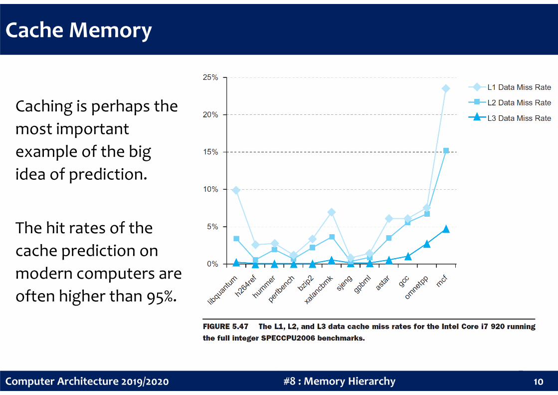
Caching is perhaps the
most important
example of the big
idea of prediction.
10#8 : Memory HierarchyComputer Architecture 2019/2020
The hit rates of the
cache prediction on
modern computers are
often higher than 95%.
Page 12
Cache Memory
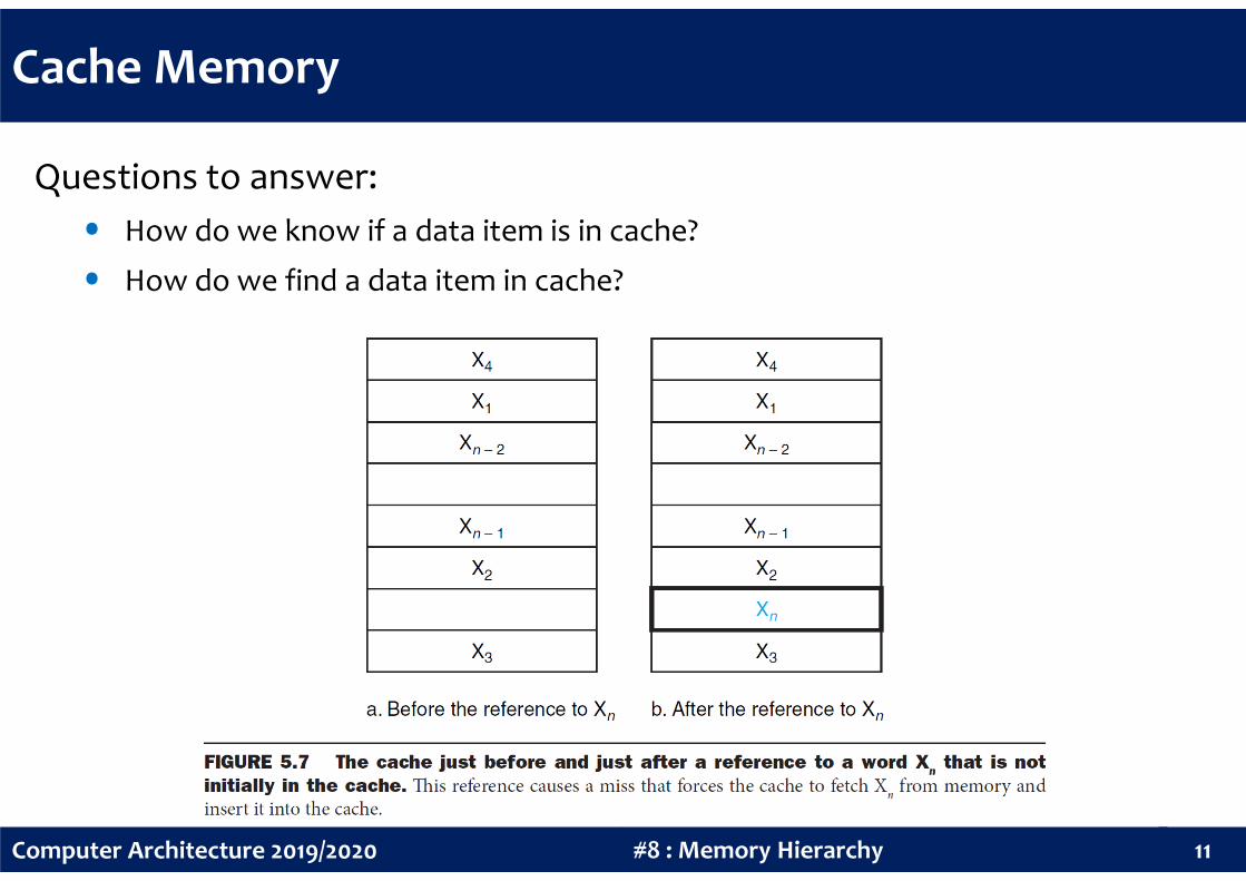
Questions to answer:
• How do we know if a data item is in cache?
• How do we find a data item in cache?
11#8 : Memory HierarchyComputer Architecture 2019/2020
Page 13
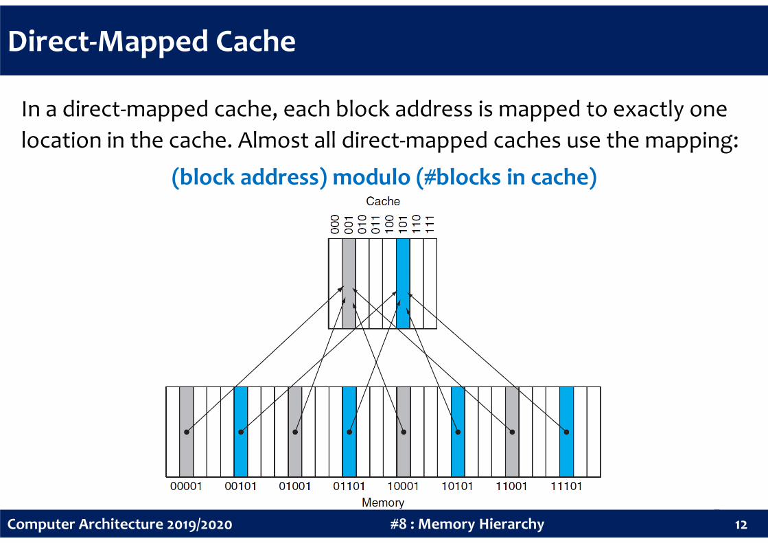
Direct-Mapped Cache
In a direct-mapped cache, each block address is mapped to exactly one
location in the cache. Almost all direct-mapped caches use the mapping:
(block address) modulo (#blocks in cache)
12#8 : Memory HierarchyComputer Architecture 2019/2020
Page 14
Direct-Mapped Cache
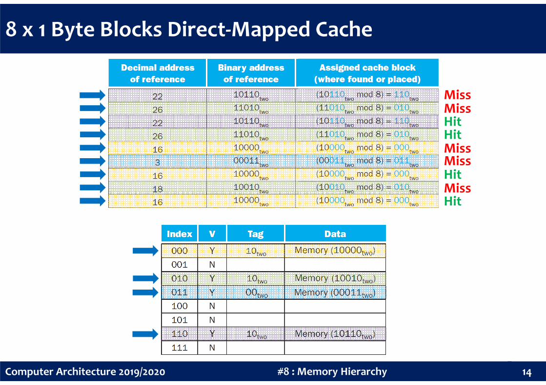
How do we compute the cache location for a given block address?
• Since the number of cache blocks is often a power of 2, use the low-order bits of
a block address to compute its cache location
How do we know which particular block is in a cache location?
• Add a set of tags to each cache location identifying the block address in cache
13#8 : Memory HierarchyComputer Architecture 2019/2020
• Add a set of tags to each cache location identifying the block address in cache
(actually, the tag only needs to contain the complementary higher-order bits)
How do we know there is valid data in a cache location?
• Add a valid bit to each cache location indicating whether a location contains
valid data (valid bit: 1 = valid data; 0 = invalid data; initially = 0)
Page 15
8 x 1 Byte Blocks Direct-Mapped Cache
MissMiss
Miss
Miss
Miss
HitHit
Hit
Hit
14#8 : Memory HierarchyComputer Architecture 2019/2020
MissHit
Page 16
1024 x 4 Byte Blocks Direct-Mapped Cache
15#8 : Memory HierarchyComputer Architecture 2019/2020
Page 17
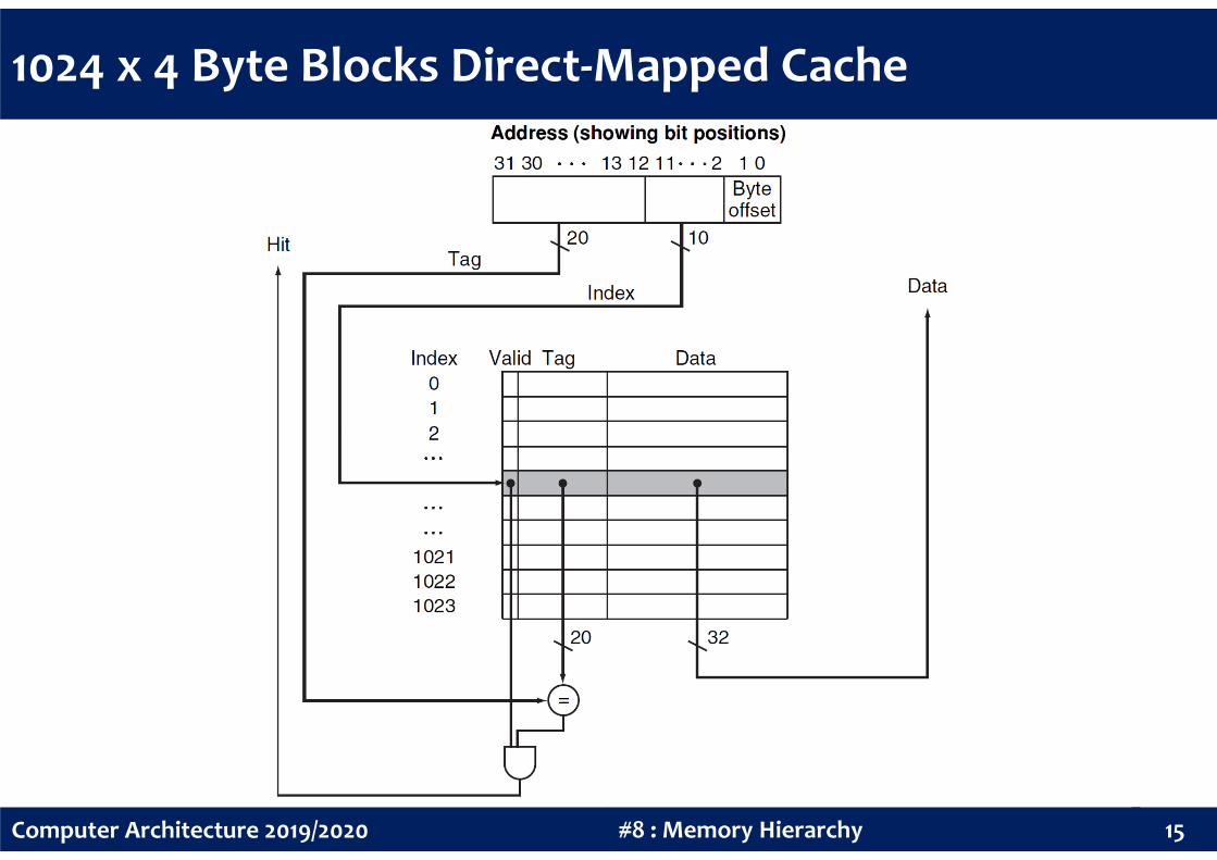
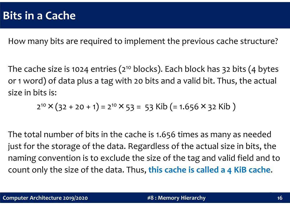
Bits in a Cache
How many bits are required to implement the previous cache structure?
The cache size is 1024 entries (210 blocks). Each block has 32 bits (4 bytes
or 1 word) of data plus a tag with 20 bits and a valid bit. Thus, the actual
size in bits is:
210×(32 + 20 + 1) = 210
×53 = 53 Kib (= 1.656×32 Kib )
16#8 : Memory HierarchyComputer Architecture 2019/2020
210×(32 + 20 + 1) = 210
×53 = 53 Kib (= 1.656×32 Kib )
The total number of bits in the cache is 1.656 times as many as needed
just for the storage of the data. Regardless of the actual size in bits, the
naming convention is to exclude the size of the tag and valid field and to
count only the size of the data. Thus, this cache is called a 4 KiB cache.
Page 18
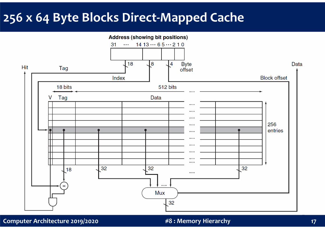
256 x 64 Byte Blocks Direct-Mapped Cache
17#8 : Memory HierarchyComputer Architecture 2019/2020
Page 19
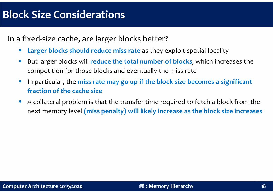
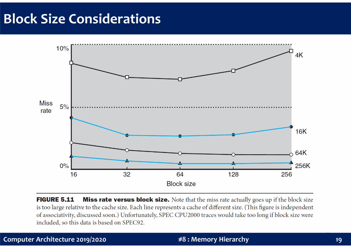
Block Size Considerations
In a fixed-size cache, are larger blocks better?
• Larger blocks should reduce miss rate as they exploit spatial locality
• But larger blocks will reduce the total number of blocks, which increases the
competition for those blocks and eventually the miss rate
• In particular, the miss rate may go up if the block size becomes a significant
fraction of the cache size
•
18#8 : Memory HierarchyComputer Architecture 2019/2020
• A collateral problem is that the transfer time required to fetch a block from the
next memory level (miss penalty) will likely increase as the block size increases
Page 20
Block Size Considerations
19#8 : Memory HierarchyComputer Architecture 2019/2020
Page 21
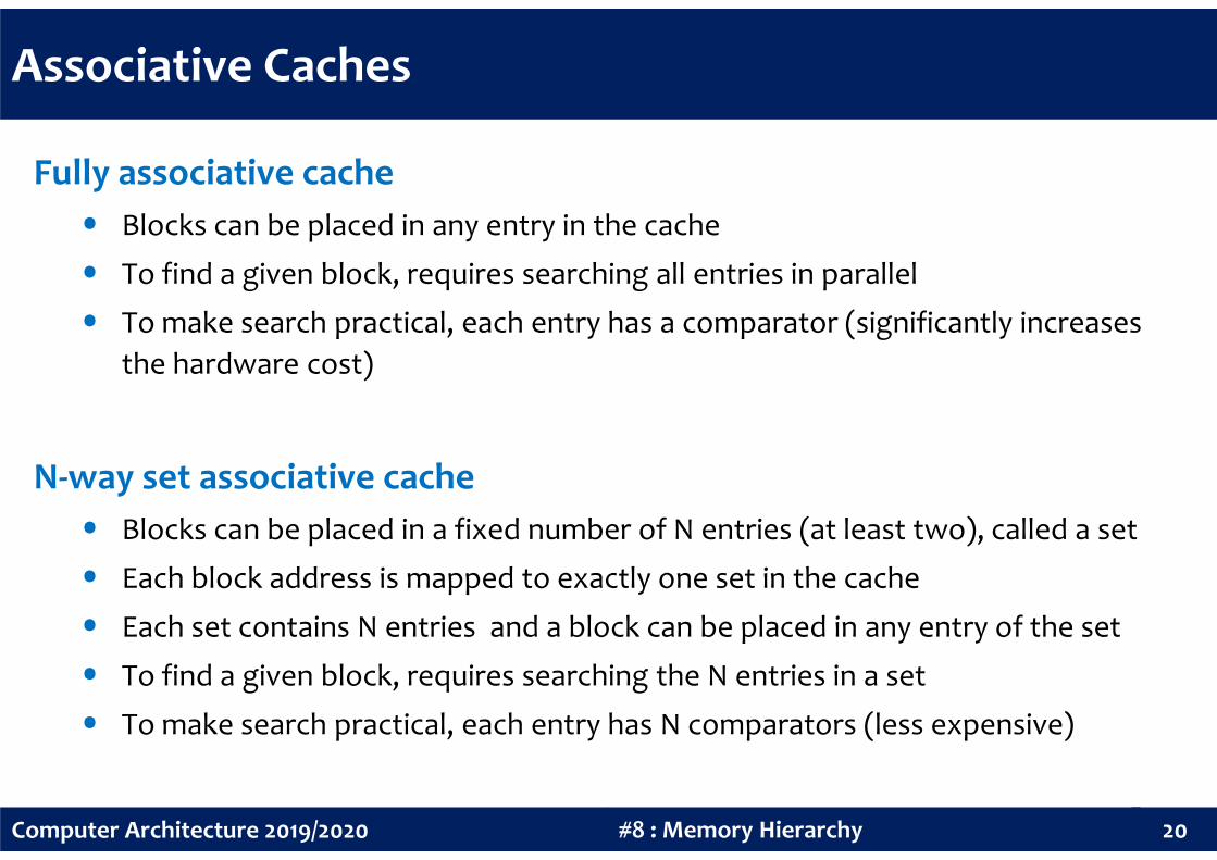
Associative Caches
Fully associative cache
• Blocks can be placed in any entry in the cache
• To find a given block, requires searching all entries in parallel
• To make search practical, each entry has a comparator (significantly increases
the hardware cost)
20#8 : Memory HierarchyComputer Architecture 2019/2020
N-way set associative cache
• Blocks can be placed in a fixed number of N entries (at least two), called a set
• Each block address is mapped to exactly one set in the cache
• Each set contains N entries and a block can be placed in any entry of the set
• To find a given block, requires searching the N entries in a set
• To make search practical, each entry has N comparators (less expensive)
Page 22
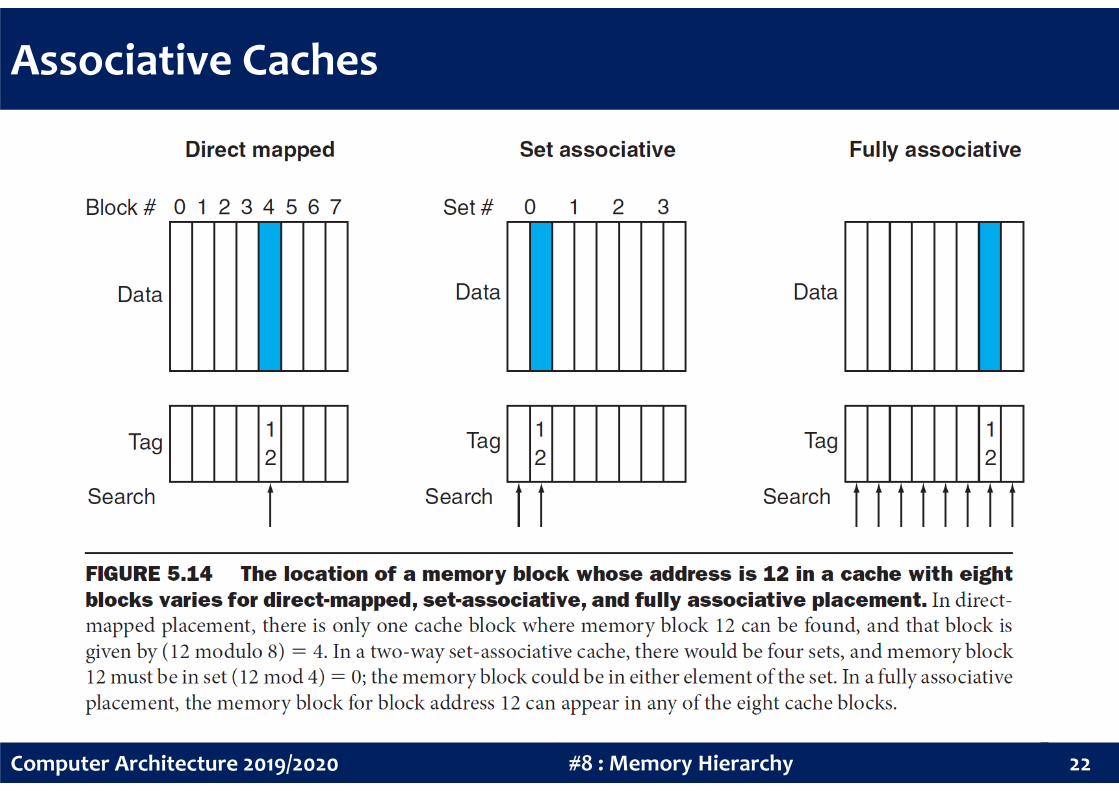
Associative Caches
In a direct-mapped cache, the entry for a memory block is given by:
(block address) modulo (#blocks in cache)
21#8 : Memory HierarchyComputer Architecture 2019/2020
In a set-associative cache, the set for a memory block is given by:
(block address) modulo (#sets in cache)
Page 23
Associative Caches
22#8 : Memory HierarchyComputer Architecture 2019/2020
Page 24
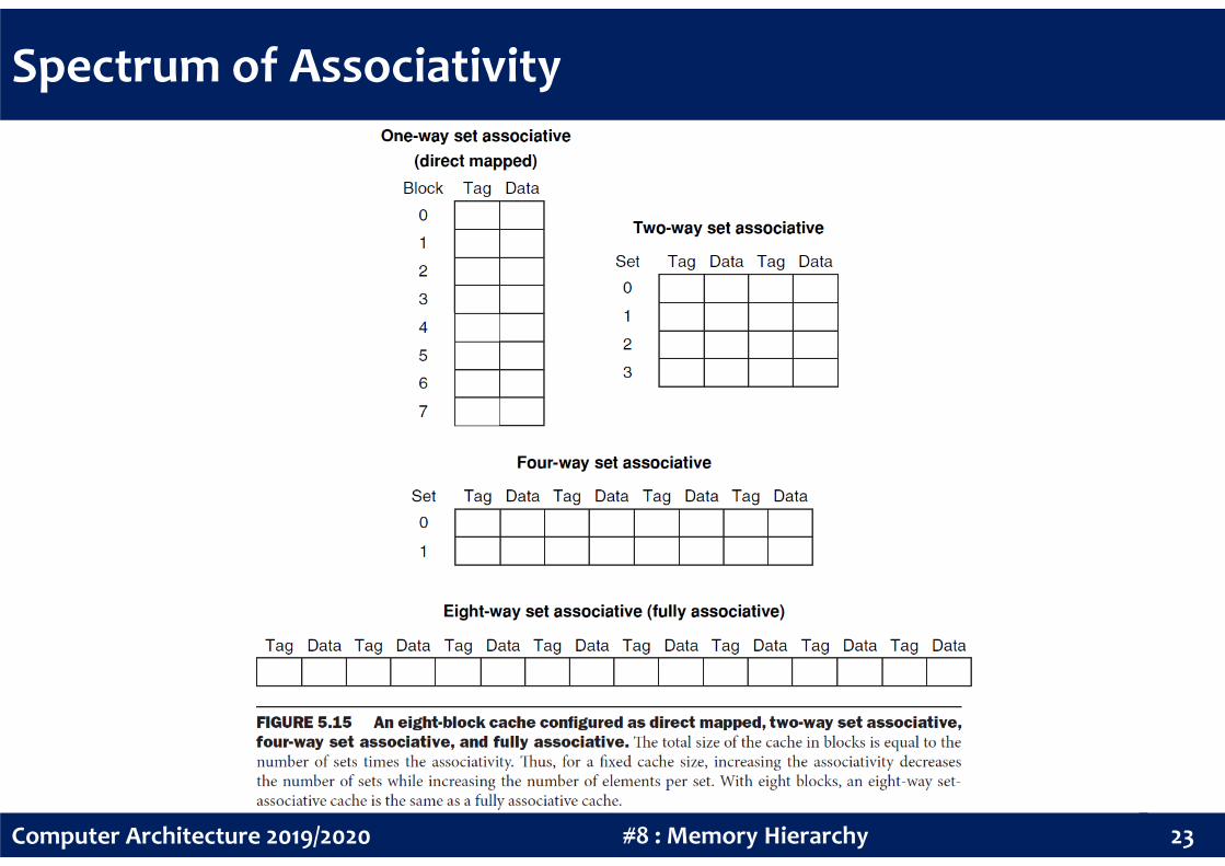
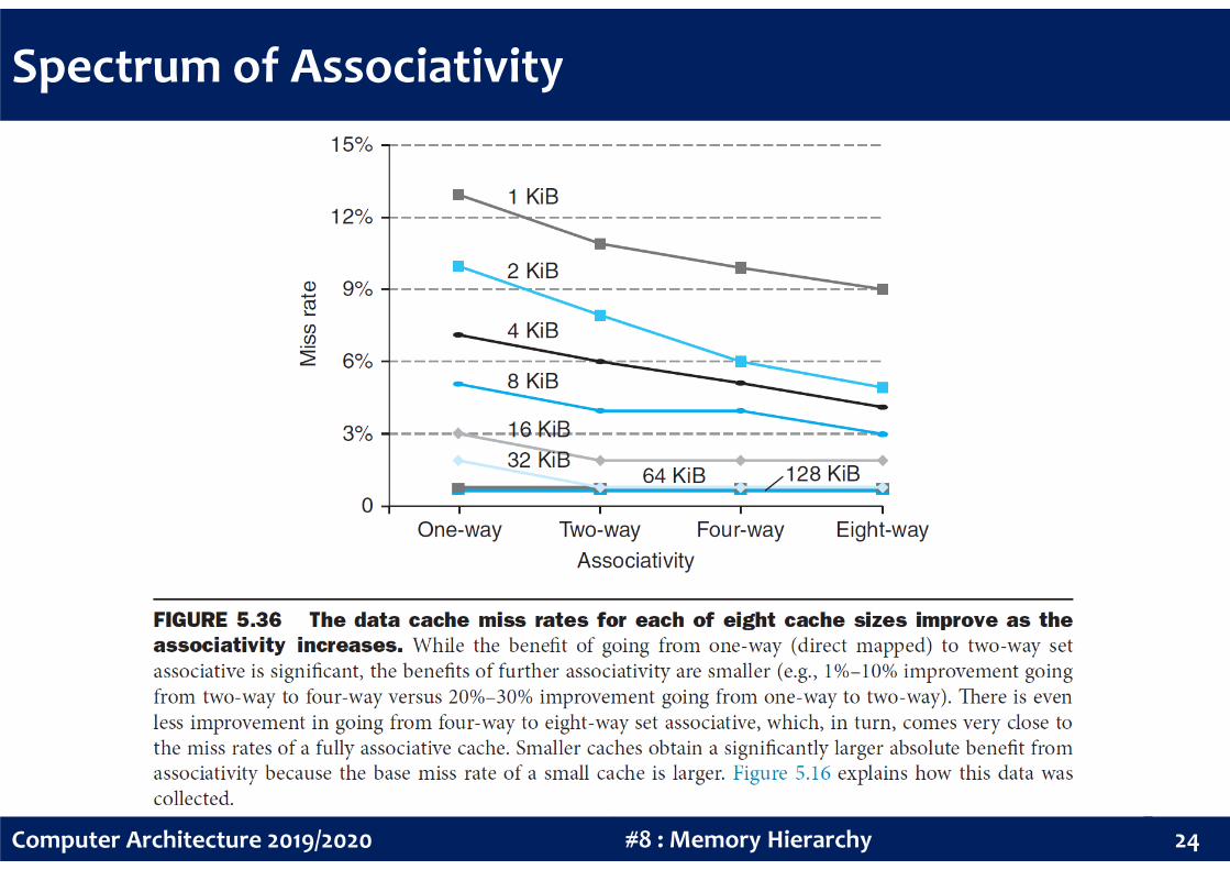
Spectrum of Associativity
23#8 : Memory HierarchyComputer Architecture 2019/2020
Page 25
Spectrum of Associativity
24#8 : Memory HierarchyComputer Architecture 2019/2020
Page 26
Replacement Policy
In an associative cache, we have a choice of where to place the
requested block, and hence a choice of which block to replace.
• In a fully associative cache, all blocks are candidates for replacement
• In a set-associative cache, we must choose among the blocks in the selected set
The most commonly used scheme is least recently used (LRU) – the
25#8 : Memory HierarchyComputer Architecture 2019/2020
The most commonly used scheme is least recently used (LRU) – the
block replaced is the one that has been unused for the longest time.
• Simple for two-way, manageable for four-way, too hard beyond that
• For a two-way can be implemented by keeping a single bit in each set and
setting the bit to indicate an element whenever that element is referenced
For high associativity caches, a random scheme gives approximately the
same performance as LRU.
Page 27
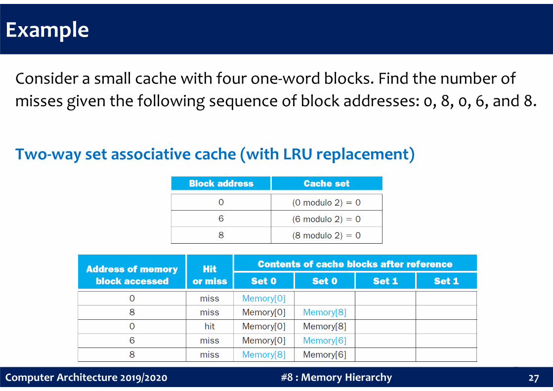
Example
Consider a small cache with four one-word blocks. Find the number of
misses given the following sequence of block addresses: 0, 8, 0, 6, and 8.
Direct-mapped cache
26#8 : Memory HierarchyComputer Architecture 2019/2020
Page 28
Example
Consider a small cache with four one-word blocks. Find the number of
misses given the following sequence of block addresses: 0, 8, 0, 6, and 8.
Two-way set associative cache (with LRU replacement)
27#8 : Memory HierarchyComputer Architecture 2019/2020
Page 29
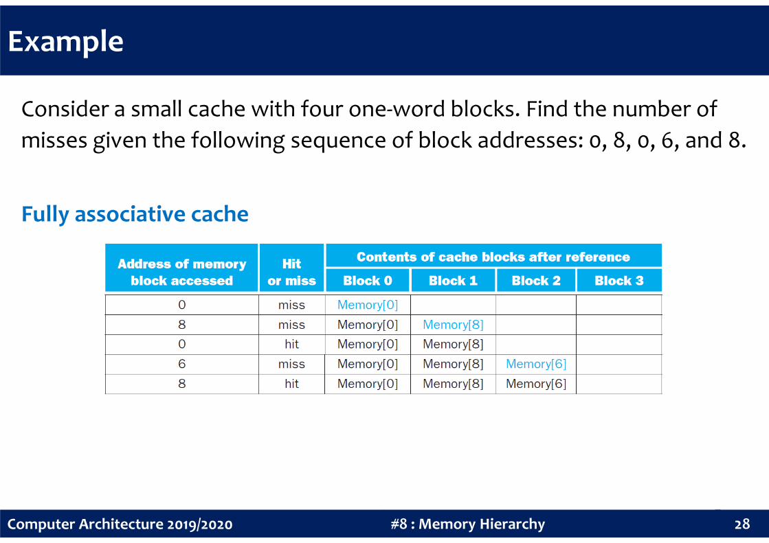
Example
Consider a small cache with four one-word blocks. Find the number of
misses given the following sequence of block addresses: 0, 8, 0, 6, and 8.
Fully associative cache
28#8 : Memory HierarchyComputer Architecture 2019/2020
Page 30
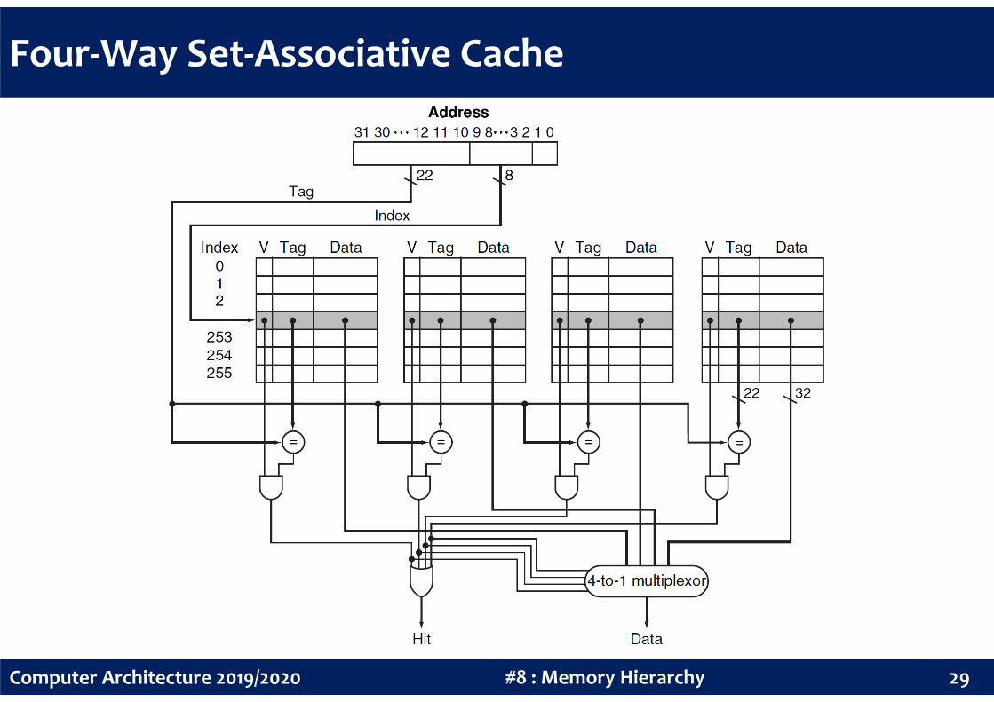
Four-Way Set-Associative Cache
29#8 : Memory HierarchyComputer Architecture 2019/2020
Page 31
Handling Cache Misses
Handling cache misses is done in collaboration with the processor
control unit. The processing of a cache miss stalls the entire processor,
essentially freezing the contents of all registers while waiting for
memory. The steps taken in a cache miss are:
• Instruct the next memory level to read the missing value
• Wait for the memory to respond (it can take multiple clock cycles)
30#8 : Memory HierarchyComputer Architecture 2019/2020
• Wait for the memory to respond (it can take multiple clock cycles)
• Update the corresponding cache line with the data received from memory
• Refetch and restart the instruction execution, this time finding it in the cache
More sophisticated processors can allow out-of-order execution of other
instructions while waiting for a cache miss.
Page 32
Handling Writes
How to handle write hits – consider a store instruction where a data-
write hit is only wrote into the cache, without changing main memory.
Then, cache and memory would have different values. In such a case,
the cache and memory are said to be inconsistent.
31#8 : Memory HierarchyComputer Architecture 2019/2020
How to handle write misses – should we fetch the corresponding block
from memory to cache and then overwrite with the word that caused
the miss (called write allocate) or should we simply write the word to
main memory (called no write allocate)?
Page 33
Caches Write-Through and Write-Back
Write-through is a scheme in which write hits always update both the
cache and the next memory level, thus ensuring that data is always
consistent between the two.
Write-back is a scheme that handles write hits by updating only the
32#8 : Memory HierarchyComputer Architecture 2019/2020
Write-back is a scheme that handles write hits by updating only the
cache, then the modified block is written to the next memory level
when it is replaced (need to keep track of modified blocks).
Page 34
Write-Through Considerations
Despite its simplicity, this scheme does not provide good performance:
• Suppose that writes take 100 clock cycles longer and that 10% of the instructions
are stores – if the base CPI (without cache misses) was 1.0, the 100 extra cycles
on every write would lead to a CPI of 1.0 + 100×10% = 11.0, thus reducing
performance by more than a factor of 10
33#8 : Memory HierarchyComputer Architecture 2019/2020
One solution is to use a write buffer to hold the data waiting to be
written to memory. Execution can continue immediately after writing
the data into the cache and into the write buffer.
• The processor only stalls if the write buffer is full when reaching a write
• When a write to main memory completes, the entry in the write buffer is freed
• If the rate at which the memory can complete writes is less than the rate at
which the processor is generating writes, no amount of buffering can help
Page 35
Write-Back Considerations
Write-back can improve performance especially when processors can
generate writes as fast or faster than the writes can be handled by main
memory.
However, write-back is more complex to implement than write-through.
• If we simply overwrite a modified block on a store instruction before knew
34#8 : Memory HierarchyComputer Architecture 2019/2020
• If we simply overwrite a modified block on a store instruction before knew
whether there is a write miss, we would destroy the contents of the block in
cache, which is not backed up in the next memory level
• Stores either require two cycles (a cycle to check for a hit followed by a cycle to
actually perform the write) or require a write buffer to hold the data to be
written while the block is checked for a hit – thus allowing the store to take only
one cycle by pipelining it
Page 36
Cache Performance
Remember the performance equation:
ClockCycle
Seconds
nInstructio
sClockCycle
ogram
nsInstructio
dClockPerioCPInCountInstructioCPUTime
××=
××=
Pr
35#8 : Memory HierarchyComputer Architecture 2019/2020
CPU time can be divided into the clock cycles that the CPU spends
executing the instructions with no misses (CPIPerfect) and the clock
cycles that the CPU spends waiting for the memory system (CPIStall).
CPIStallCPIPerfectCPI +=
Page 37
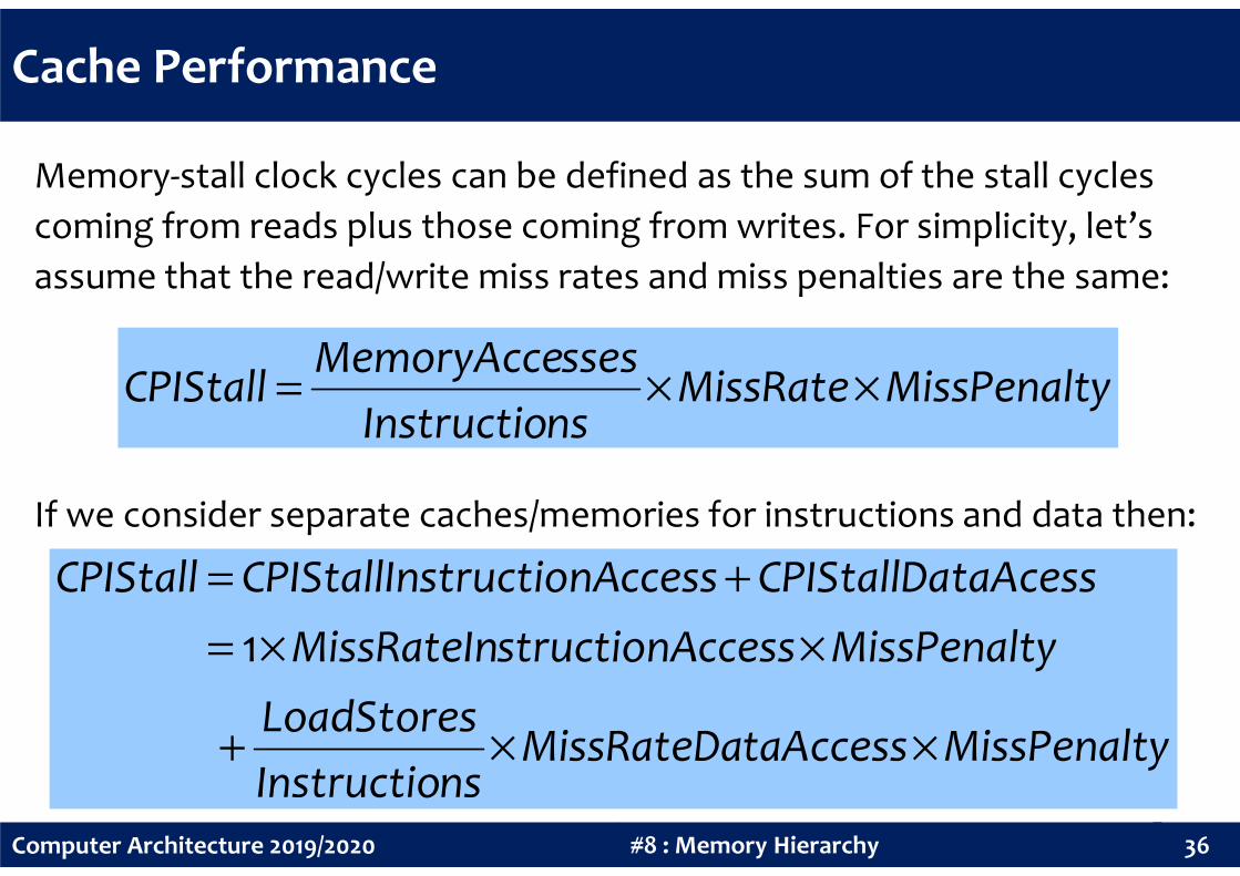
Cache Performance
Memory-stall clock cycles can be defined as the sum of the stall cycles
coming from reads plus those coming from writes. For simplicity, let’s
assume that the read/write miss rates and miss penalties are the same:
yMissPenaltMissRatensInstructio
ssesMemoryAcceCPIStall ××=
36#8 : Memory HierarchyComputer Architecture 2019/2020
If we consider separate caches/memories for instructions and data then:
nsInstructio
yMissPenalttaAccessMissRateDansInstructio
LoadStores
yMissPenaltccessstructionAMissRateIn
taAcessCPIStallDaccessstructionACPIStallInCPIStall
××+
××=
+=
1
Page 38
Example
Assume a miss rate of 2% for the instruction cache and of 4% for the data
cache, a miss penalty of 100 cycles for all misses, and a frequency of 36%
of loads and stores. If the CPI is 2 without memory stalls, determine how
much faster the processor runs with a perfect cache that never misses.
CPI memory stall for instructions and data access:
37#8 : Memory HierarchyComputer Architecture 2019/2020
CPI memory stall for instructions and data access:
• CPIStallInstructionAccess = 1 × 0.02 × 100 = 2.00
• CPIStallDataAccess = 0.36 × 0.04 × 100 = 1.44
• CPIStall = 2.00 + 1.44 = 3.44
Accordingly, the total CPI including memory stalls is:
• CPI = 2 + 3.44 = 5.44
Performance with perfect cache is better by 2.72 = 5.44 / 2
Page 39
Clock Rate Improvement
What happens if the processor is made faster but memory access is not?
Suppose we speed-up the clock rate by a factor of 2:
• The previous miss penalty of 100 cycles is now 200 cycles
• CPIStallInstructionAccess = 1 × 0.02 × 200 = 4.00
• CPIStallDataAccess = 0.36 × 0.04 × 200 = 2.88
38#8 : Memory HierarchyComputer Architecture 2019/2020
• CPIStallDataAccess = 0.36 × 0.04 × 200 = 2.88
• CPIStall = 4.00 + 2.88 = 6.88
• CPI = 2 + 6.88 = 8.88
• The fraction of time spent on memory stalls would have risen from 63% to 77%
(3.44 / 5.44 = 63% and 6.88 / 8.88 = 77%)
• The total execution time of a program is better by 1.23 = 5.44 / (8.88 / 2)
Page 40
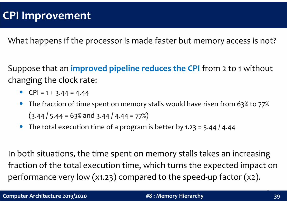
CPI Improvement
What happens if the processor is made faster but memory access is not?
Suppose that an improved pipeline reduces the CPI from 2 to 1 without
changing the clock rate:
• CPI = 1 + 3.44 = 4.44
• The fraction of time spent on memory stalls would have risen from 63% to 77%
39#8 : Memory HierarchyComputer Architecture 2019/2020
• The fraction of time spent on memory stalls would have risen from 63% to 77%
(3.44 / 5.44 = 63% and 3.44 / 4.44 = 77%)
• The total execution time of a program is better by 1.23 = 5.44 / 4.44
In both situations, the time spent on memory stalls takes an increasing
fraction of the total execution time, which turns the expected impact on
performance very low (x1.23) compared to the speed-up factor (x2).
Page 41
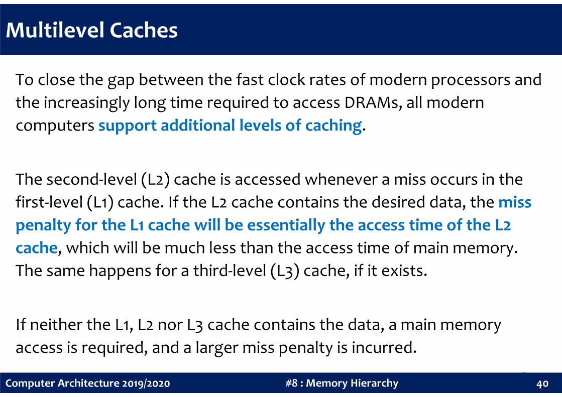
Multilevel Caches
To close the gap between the fast clock rates of modern processors and
the increasingly long time required to access DRAMs, all modern
computers support additional levels of caching.
The second-level (L2) cache is accessed whenever a miss occurs in the
first-level (L1) cache. If the L2 cache contains the desired data, the miss
40#8 : Memory HierarchyComputer Architecture 2019/2020
first-level (L1) cache. If the L2 cache contains the desired data, the miss
penalty for the L1 cache will be essentially the access time of the L2
cache, which will be much less than the access time of main memory.
The same happens for a third-level (L3) cache, if it exists.
If neither the L1, L2 nor L3 cache contains the data, a main memory
access is required, and a larger miss penalty is incurred.
Page 42
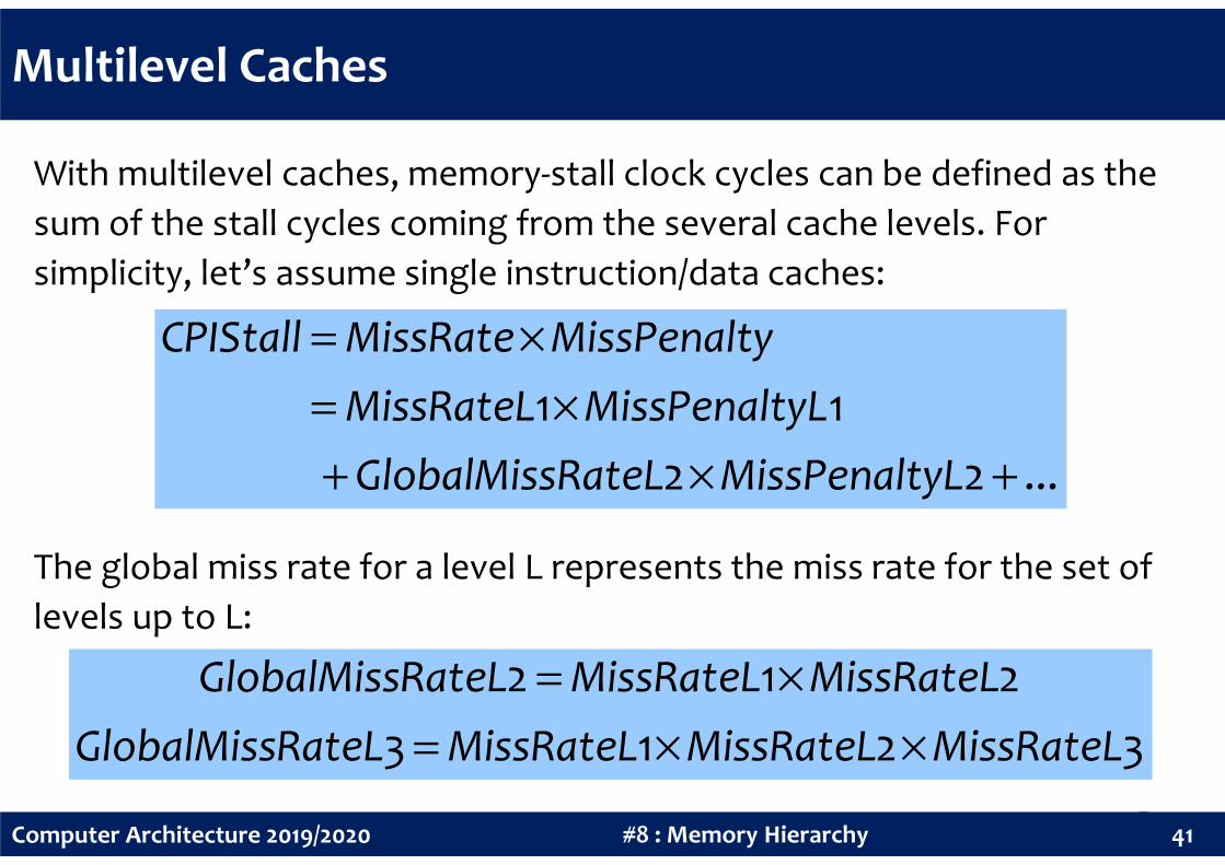
Multilevel Caches
With multilevel caches, memory-stall clock cycles can be defined as the
sum of the stall cycles coming from the several cache levels. For
simplicity, let’s assume single instruction/data caches:
11×=
×=
yLMissPenaltMissRateL
yMissPenaltMissRateCPIStall
41#8 : Memory HierarchyComputer Architecture 2019/2020
The global miss rate for a level L represents the miss rate for the set of
levels up to L:
...22
11
+×+ yLMissPenaltRateLGlobalMiss
yLMissPenaltMissRateL
3213
212
MissRateLMissRateLMissRateLRateLGlobalMiss
MissRateLMissRateLRateLGlobalMiss
××=
×=
Page 43
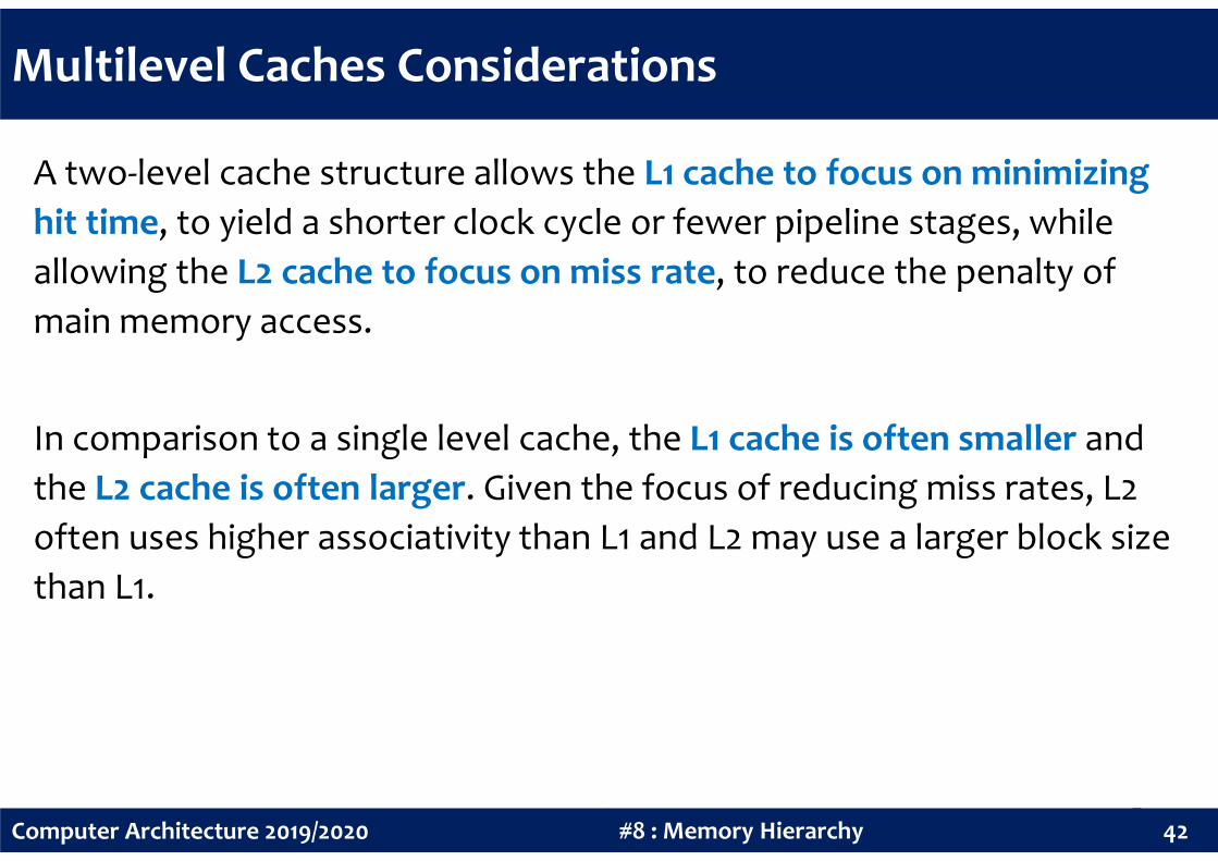
Multilevel Caches Considerations
A two-level cache structure allows the L1 cache to focus on minimizing
hit time, to yield a shorter clock cycle or fewer pipeline stages, while
allowing the L2 cache to focus on miss rate, to reduce the penalty of
main memory access.
In comparison to a single level cache, the L1 cache is often smaller and
42#8 : Memory HierarchyComputer Architecture 2019/2020
In comparison to a single level cache, the L1 cache is often smaller and
the L2 cache is often larger. Given the focus of reducing miss rates, L2
often uses higher associativity than L1 and L2 may use a larger block size
than L1.
Page 44
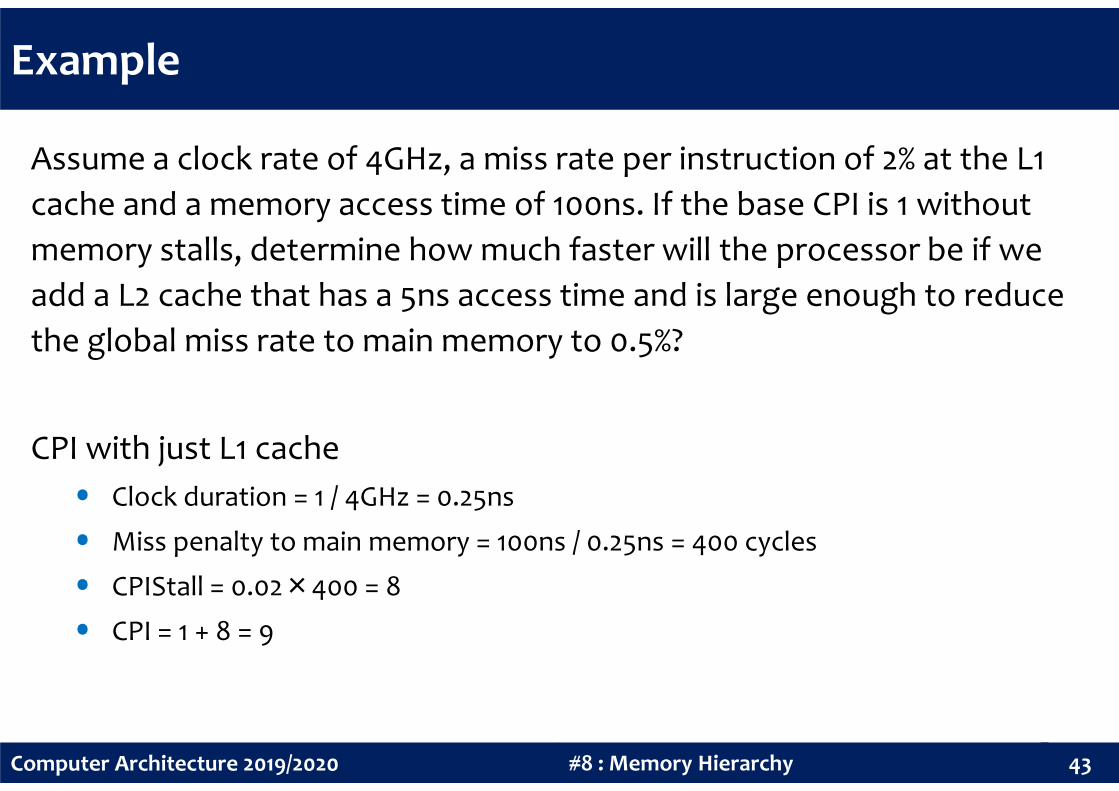
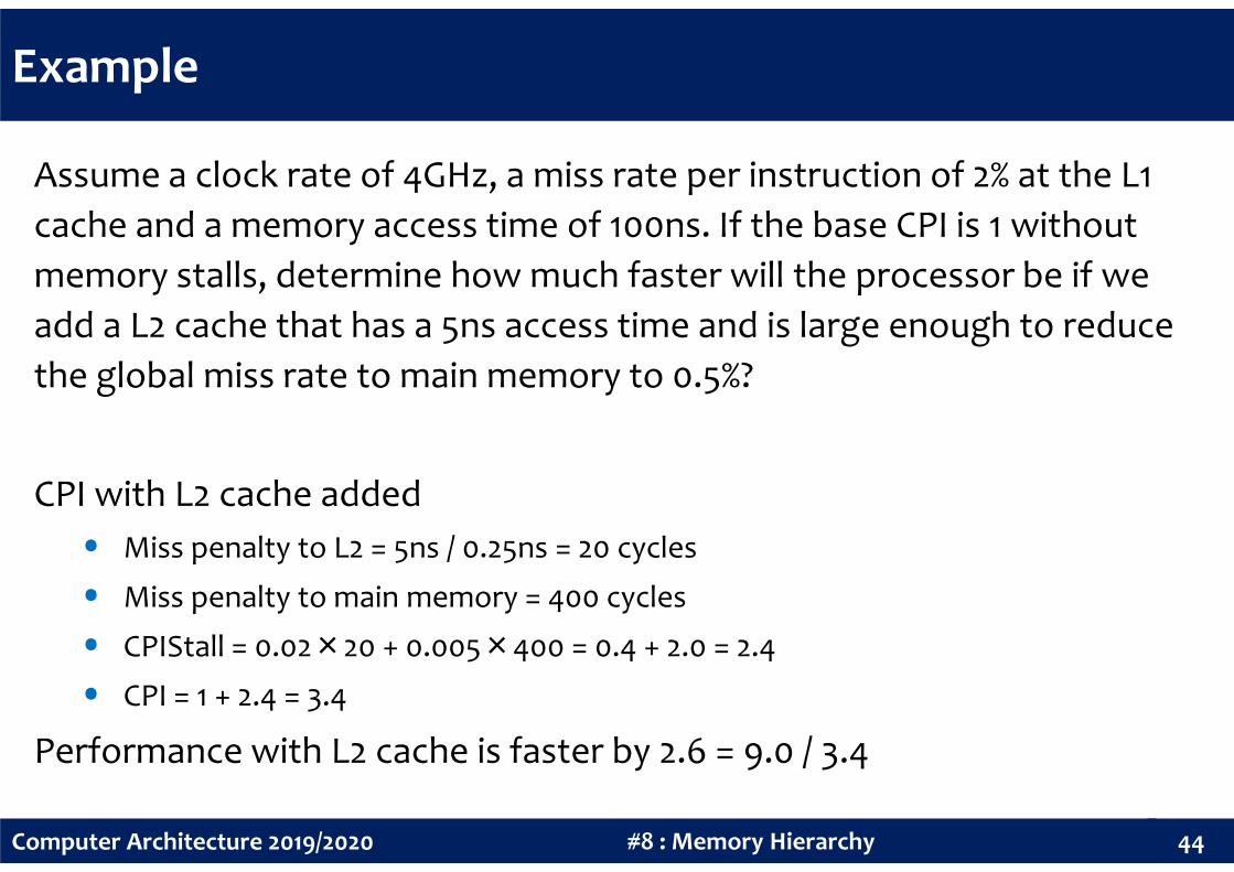
Example
Assume a clock rate of 4GHz, a miss rate per instruction of 2% at the L1
cache and a memory access time of 100ns. If the base CPI is 1 without
memory stalls, determine how much faster will the processor be if we
add a L2 cache that has a 5ns access time and is large enough to reduce
the global miss rate to main memory to 0.5%?
43#8 : Memory HierarchyComputer Architecture 2019/2020
CPI with just L1 cache
• Clock duration = 1 / 4GHz = 0.25ns
• Miss penalty to main memory = 100ns / 0.25ns = 400 cycles
• CPIStall = 0.02×400 = 8
• CPI = 1 + 8 = 9
Page 45
Example
Assume a clock rate of 4GHz, a miss rate per instruction of 2% at the L1
cache and a memory access time of 100ns. If the base CPI is 1 without
memory stalls, determine how much faster will the processor be if we
add a L2 cache that has a 5ns access time and is large enough to reduce
the global miss rate to main memory to 0.5%?
44#8 : Memory HierarchyComputer Architecture 2019/2020
CPI with L2 cache added
• Miss penalty to L2 = 5ns / 0.25ns = 20 cycles
• Miss penalty to main memory = 400 cycles
• CPIStall = 0.02×20 + 0.005×400 = 0.4 + 2.0 = 2.4
• CPI = 1 + 2.4 = 3.4
Performance with L2 cache is faster by 2.6 = 9.0 / 3.4
Page 46
Virtual Memory
Virtual memory is a technique that uses main memory as a cache for
secondary storage.
• Allows the execution of processes that are not entirely in memory
• Abstracts main memory into an extremely large uniform array of storage
• Frees programmers from the concerns of memory storage limitations
45#8 : Memory HierarchyComputer Architecture 2019/2020
Code needs to be in memory to execute, but entire program rarely used:
• Code to handle unusual situations is almost never executed
• Large data structures often allocate more memory than they actually need
• Even if the entire program is used, it is not all needed at same time
Page 47
Virtual Memory
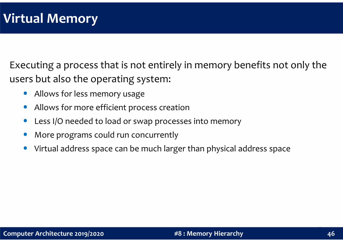
Executing a process that is not entirely in memory benefits not only the
users but also the operating system:
• Allows for less memory usage
• Allows for more efficient process creation
• Less I/O needed to load or swap processes into memory
46#8 : Memory HierarchyComputer Architecture 2019/2020
• Less I/O needed to load or swap processes into memory
• More programs could run concurrently
• Virtual address space can be much larger than physical address space
Page 48
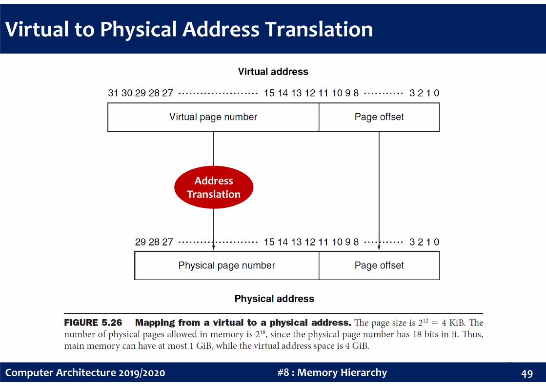
Virtual Memory
Although the concepts at work in virtual memory and in caches are the
same, they use different terminology:
• A virtual memory block is called a page
• A physical memory block is called a frame
• A virtual memory miss is called a page fault
47#8 : Memory HierarchyComputer Architecture 2019/2020
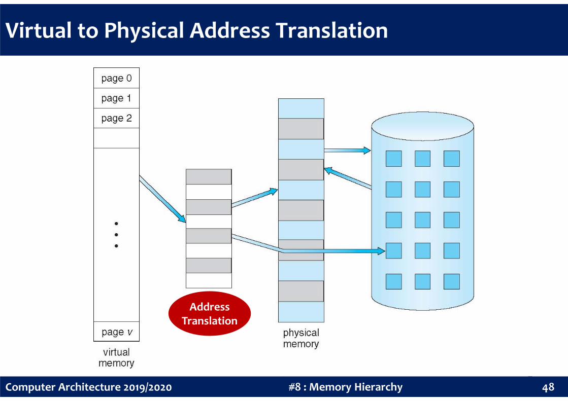
With virtual memory, the processor produces a virtual address, which is
translated by a combination of hardware and software to a physical
address, which in turn can be used to access main memory. This process
is called address mapping or address translation.
Page 49
Virtual to Physical Address Translation
48#8 : Memory HierarchyComputer Architecture 2019/2020
AddressTranslation
Page 50
Virtual to Physical Address Translation
AddressTranslation
49#8 : Memory HierarchyComputer Architecture 2019/2020
Translation
Page 51
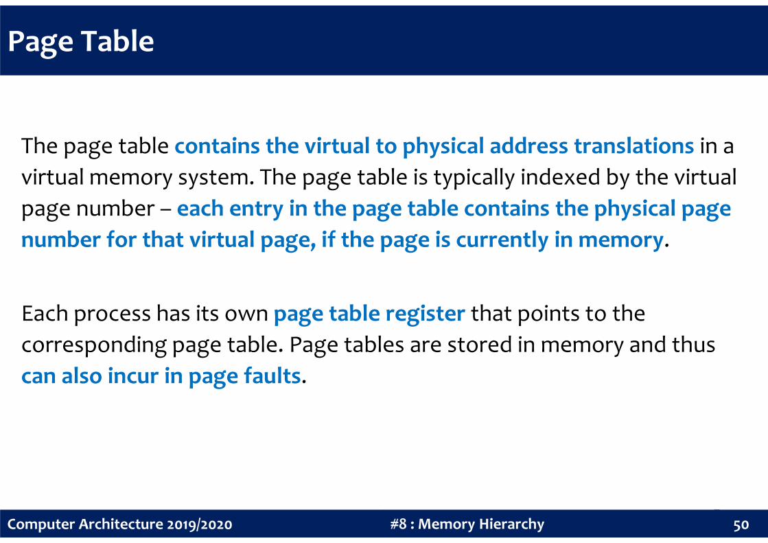
Page Table
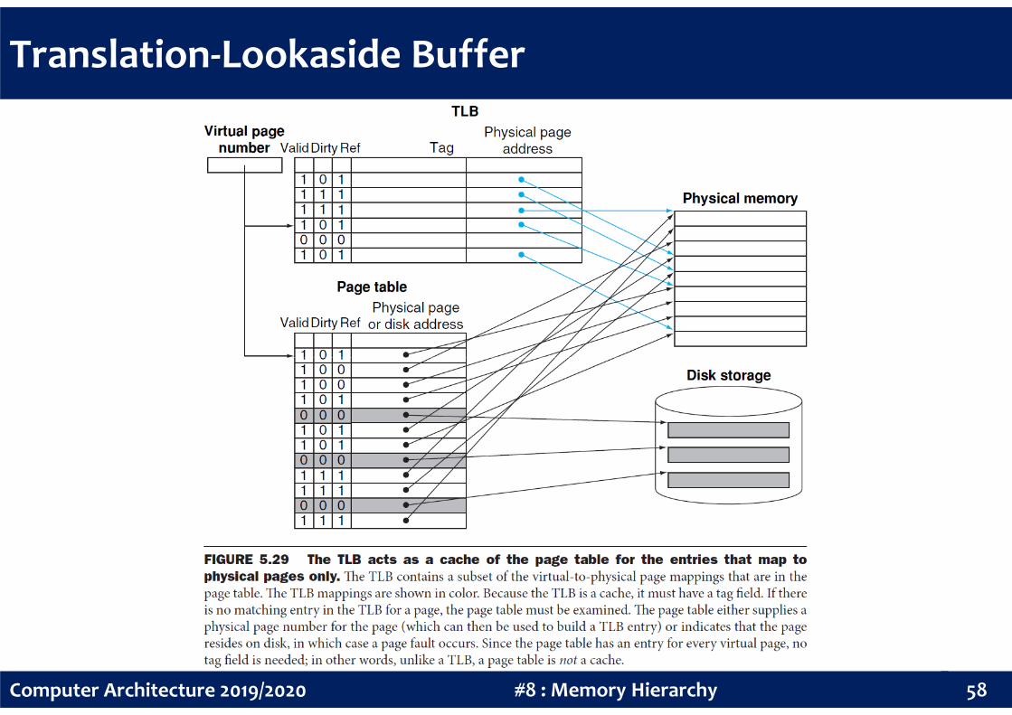
The page table contains the virtual to physical address translations in a
virtual memory system. The page table is typically indexed by the virtual
page number – each entry in the page table contains the physical page
number for that virtual page, if the page is currently in memory.
50#8 : Memory HierarchyComputer Architecture 2019/2020
Each process has its own page table register that points to the
corresponding page table. Page tables are stored in memory and thus
can also incur in page faults.
Page 52
Page Table
51#8 : Memory HierarchyComputer Architecture 2019/2020
Page 53
Handling Page Faults
On a page fault, the page must be fetched from the next memory level
(usually flash memory or magnetic disks), which can take millions of
clock cycles to process.
The procedure for handling a page fault is straightforward:
• Find a free frame in memory and bring in the missing page from backing store
52#8 : Memory HierarchyComputer Architecture 2019/2020
• Find a free frame in memory and bring in the missing page from backing store
• Reset page table to indicate that page is now in memory
• Restart the instruction that caused the page fault
To reduce page fault rate, fully associative placement of pages in
memory and smart replacement algorithms are used together with
large enough page sizes. Sizes from 4 KiB to 16 KiB are typical today.
Page 54
Handling Page Faults
53#8 : Memory HierarchyComputer Architecture 2019/2020
Page 55
Page Replacement
When a page fault occurs, if all pages in main memory are in use, the
operating system must choose a page to replace. Because we want to
minimize the number of page faults, most operating systems try to
choose a page that will not be needed in the near future.
Two page transfers are required – one to write the replaced page back
54#8 : Memory HierarchyComputer Architecture 2019/2020
Two page transfers are required – one to write the replaced page back
to secondary storage and another to bring the faulty page in. This
overhead can be reduced by using a modify (or dirty) bit per page.
• The dirty bit is set whenever a page in memory is modified
• When a page is selected for replacement, if its dirty bit is unset, the page has not
been modified since it was loaded and we can avoid writing it back to secondary
storage since it is already there
Page 56
Page Replacement Algorithms
Several page replacement algorithms exist:
• FIFO – First-In First-Out
• LRU – Least Recently Used
• Second chance
• Clock
55#8 : Memory HierarchyComputer Architecture 2019/2020
• Clock
• NRU – Not Recently Used
• LFU – Least Frequently Used
• Aging
Page 57
Translation-Lookaside Buffer
Address translation appears to require extra memory references:
• One to access the page table
• Another to access the actual data
But access to page tables has good locality. Accordingly, modern
56#8 : Memory HierarchyComputer Architecture 2019/2020
But access to page tables has good locality. Accordingly, modern
processors include a fast cache, called translation-lookaside buffer (TLB),
that keeps track of recently used address translations to try to avoid
access the page table.
Page 58
Translation-Lookaside Buffer
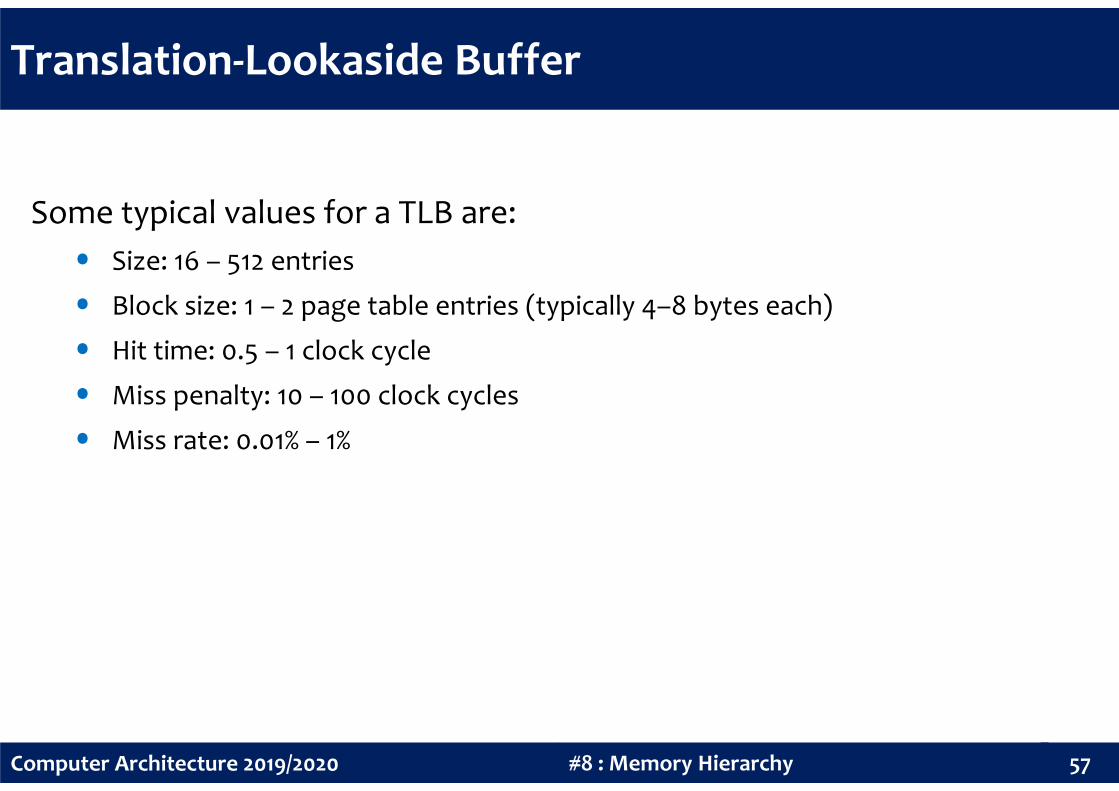
Some typical values for a TLB are:
• Size: 16 – 512 entries
• Block size: 1 – 2 page table entries (typically 4–8 bytes each)
• Hit time: 0.5 – 1 clock cycle
• Miss penalty: 10 – 100 clock cycles
57#8 : Memory HierarchyComputer Architecture 2019/2020
• Miss penalty: 10 – 100 clock cycles
• Miss rate: 0.01% – 1%
Page 59
Translation-Lookaside Buffer
58#8 : Memory HierarchyComputer Architecture 2019/2020
Page 60
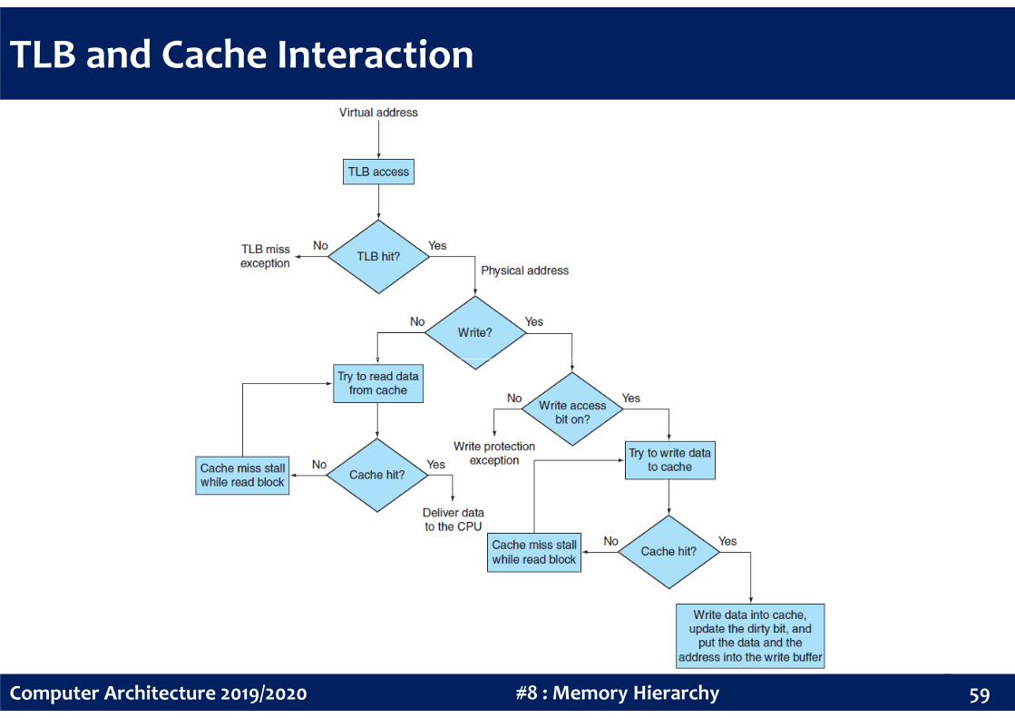
TLB and Cache Interaction
59#8 : Memory HierarchyComputer Architecture 2019/2020
Page 61
TLB and Cache Interaction
TLBfully associative
32-bit addresses4KiB pages
60#8 : Memory HierarchyComputer Architecture 2019/2020
Cachedirect-mapped