806 IEEE TRANSACTIONS ON ELECTROMAGNETIC COMPATIBILITY, VOL. 53, NO. 3, AUGUST 2011
DC-DC Buck Converter EMI Reduction Using PCBLayout Modification
Ankit Bhargava, Member, IEEE, David Pommerenke, Senior Member, IEEE, Keong W. Kam, Member, IEEE,Federico Centola, and Cheng Wei Lam
Abstract—The paper treats the effect of layout on the electro-magnetic interference (EMI) of buck converters. An optimized lay-out design for dc-dc synchronous buck converter is proposed forEMI reduction. Six different layout versions are analyzed with re-spect to loop area, loop inductance, radiating dipole moments, andfar-field radiation. Optimizations are done with respect to field-effect transistor (FET), decoupling capacitor and via placement.Passive full-wave simulations are used to estimate and verify theloop inductance and far-field emissions. Those are compared withmeasurements. A gigahertz transverse electromagnetic (GTEM)cell is used to quantify the dipole moments in the printed cir-cuit board (PCB) for estimating the far field and comparing tomeasurement.
Index Terms—DC-DC buck converter, EMI/EMC, loop induc-tance, PCB layout.
I. INTRODUCTION
THE switching nature of dc-dc synchronous buck converterscan cause significant electromagnetic interference (EMI)
issues. Three mechanisms contribute to the EMI:1) the harmonics of the switching frequency, usually below
30 MHz;2) the ringing of the phase voltage loop [1], [2], usually
between 50–300 MHz; this problem is addressed in thefollowing work; the ringing is caused by a loop formedfrom the high-side (HS) FET (on), the low-side (LS) FET(off), and the input decoupling capacitors;
3) and, the reverse recovery noise usually seen above200 MHz [13].
There are circuit (KVL, KCL) and layout (electromagnetic)related methods for controlling the EMI. This paper mainlyfocuses on the layout related methods. However, it is worth tobriefly review circuit related methods.
A popular choice to suppress the ringing is an RC snubbercircuit, which is placed across the low-side FET to add RFloss [10], [11]. For low-inductance loops, an RL snubber addedin series within the loop offers advantages in suppressing the
Manuscript received January 7, 2010; revised June 19, 2010; accepted August24, 2010. Date of publication July 12, 2011; date of current version August 18,2011.
A. Bhargava, D. Pommerenke, and K. W. Kam are with the MissouriUniversity of Science and Technology (formerly the University of Missouri-Rolla) Electromagnetic Compatibility (EMC) Laboratory, Rolla, MO 65401USA (e-mail: [email protected]; [email protected]; [email protected]).
Digital Object Identifier 10.1109/TEMC.2011.2145421
Fig. 1. Equivalent for the low side FET.
ringing [3], or, the ESR of capacitors can be used to suppressthe ringing.
The selection of MOSFETs and its drive circuitry will alsoaffect the ringing. Ringing is influenced by the switching times,values of Coss, and losses in the output capacitance. To allow usto concentrate on layout effects, the same driver and FET com-bination was chosen throughout this paper: Intersil ISL6269IRZas PWM controller, FDMS8692 as HS FET, and FDMS8672 asLS FET.
Another additional loss contributing to the attenuation of theringing is the real part of the output capacitance Coss . We assigna value “Ross” to it, which can be determined by measurements[4], [14]. An equivalent circuit for the low-side FET, when it isturned OFF, can be realized, as shown in Fig. 1.
More layout-related known methods are:1) Reducing the loop inductance: Two plausible, but not al-
ways valid lines of thought show that a reduced loop induc-tance is likely to reduce the EMI. The resonance frequencymoves up, however, the excitation rolls off with frequency,thus the loop will be excited less strongly. Second, if thelosses of the loop stay constant, then the attenuation willincrease, as the ratio of L/R diminishes [2], [3].
2) Layout optimization for geometry-based design strategy.3) Input and output filtering [2].This paper mainly focuses on the layout optimization methods
and gives an insight into the physical structure of the loops tosuppress EMI. This way EMI issues can be dealt on the PCBlevel.
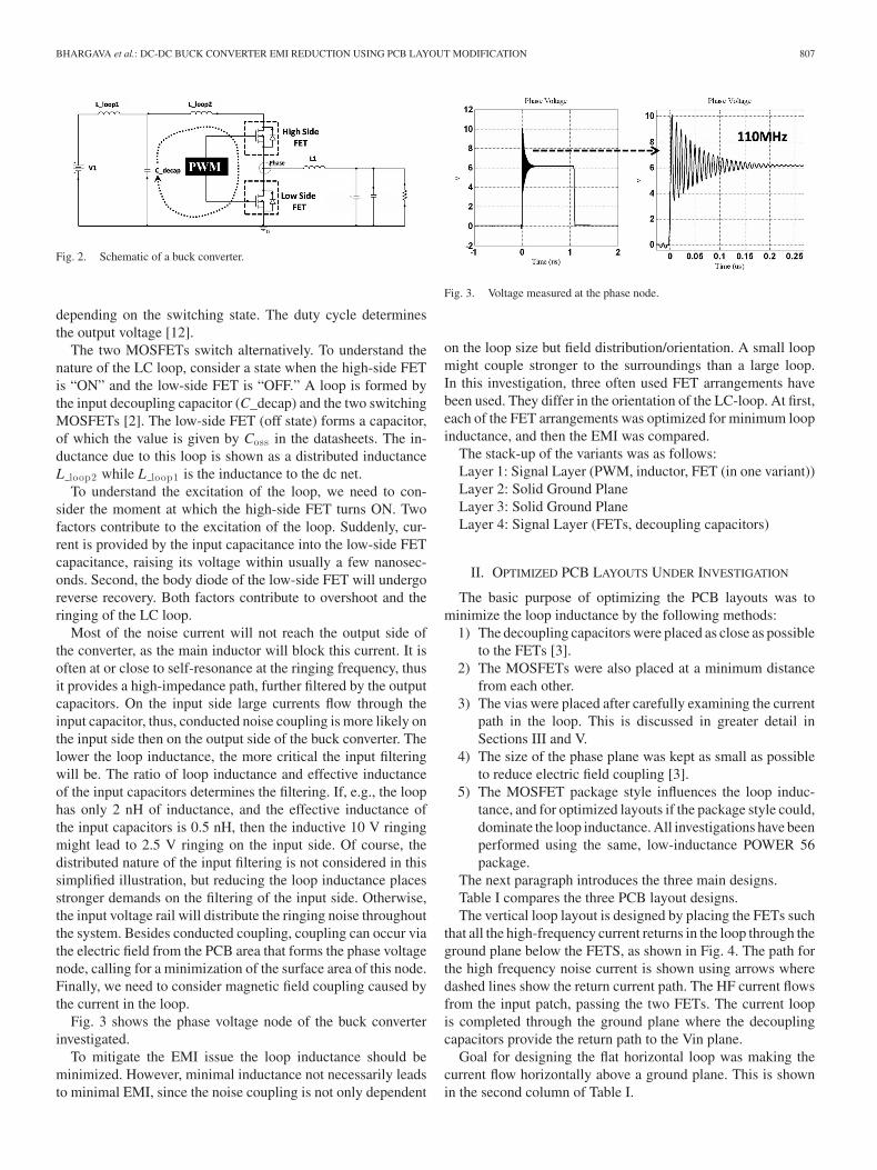
Fig. 2. shows the circuit schematic of a buck converter.A synchronous buck converter is a step down dc-dc con-
verter. It uses two complimentary switches and an inductor anda capacitor at the output stage. The two MOSFETs switch al-ternatively connecting the inductor to the source. The energyis stored in the inductor and then discharged into the load
BHARGAVA et al.: DC-DC BUCK CONVERTER EMI REDUCTION USING PCB LAYOUT MODIFICATION 807
Fig. 2. Schematic of a buck converter.
depending on the switching state. The duty cycle determinesthe output voltage [12].
The two MOSFETs switch alternatively. To understand thenature of the LC loop, consider a state when the high-side FETis “ON” and the low-side FET is “OFF.” A loop is formed bythe input decoupling capacitor (C_decap) and the two switchingMOSFETs [2]. The low-side FET (off state) forms a capacitor,of which the value is given by Coss in the datasheets. The in-ductance due to this loop is shown as a distributed inductanceL loop2 while L loop1 is the inductance to the dc net.
To understand the excitation of the loop, we need to con-sider the moment at which the high-side FET turns ON. Twofactors contribute to the excitation of the loop. Suddenly, cur-rent is provided by the input capacitance into the low-side FETcapacitance, raising its voltage within usually a few nanosec-onds. Second, the body diode of the low-side FET will undergoreverse recovery. Both factors contribute to overshoot and theringing of the LC loop.
Most of the noise current will not reach the output side ofthe converter, as the main inductor will block this current. It isoften at or close to self-resonance at the ringing frequency, thusit provides a high-impedance path, further filtered by the outputcapacitors. On the input side large currents flow through theinput capacitor, thus, conducted noise coupling is more likely onthe input side then on the output side of the buck converter. Thelower the loop inductance, the more critical the input filteringwill be. The ratio of loop inductance and effective inductanceof the input capacitors determines the filtering. If, e.g., the loophas only 2 nH of inductance, and the effective inductance ofthe input capacitors is 0.5 nH, then the inductive 10 V ringingmight lead to 2.5 V ringing on the input side. Of course, thedistributed nature of the input filtering is not considered in thissimplified illustration, but reducing the loop inductance placesstronger demands on the filtering of the input side. Otherwise,the input voltage rail will distribute the ringing noise throughoutthe system. Besides conducted coupling, coupling can occur viathe electric field from the PCB area that forms the phase voltagenode, calling for a minimization of the surface area of this node.Finally, we need to consider magnetic field coupling caused bythe current in the loop.
Fig. 3 shows the phase voltage node of the buck converterinvestigated.
To mitigate the EMI issue the loop inductance should beminimized. However, minimal inductance not necessarily leadsto minimal EMI, since the noise coupling is not only dependent
Fig. 3. Voltage measured at the phase node.
on the loop size but field distribution/orientation. A small loopmight couple stronger to the surroundings than a large loop.In this investigation, three often used FET arrangements havebeen used. They differ in the orientation of the LC-loop. At first,each of the FET arrangements was optimized for minimum loopinductance, and then the EMI was compared.
The stack-up of the variants was as follows:Layer 1: Signal Layer (PWM, inductor, FET (in one variant))Layer 2: Solid Ground PlaneLayer 3: Solid Ground PlaneLayer 4: Signal Layer (FETs, decoupling capacitors)
II. OPTIMIZED PCB LAYOUTS UNDER INVESTIGATION
The basic purpose of optimizing the PCB layouts was tominimize the loop inductance by the following methods:
1) The decoupling capacitors were placed as close as possibleto the FETs [3].
2) The MOSFETs were also placed at a minimum distancefrom each other.
3) The vias were placed after carefully examining the currentpath in the loop. This is discussed in greater detail inSections III and V.
4) The size of the phase plane was kept as small as possibleto reduce electric field coupling [3].
5) The MOSFET package style influences the loop induc-tance, and for optimized layouts if the package style could,dominate the loop inductance. All investigations have beenperformed using the same, low-inductance POWER 56package.
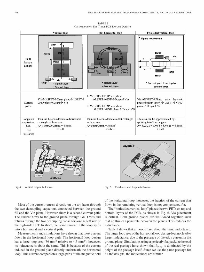
The next paragraph introduces the three main designs.Table I compares the three PCB layout designs.The vertical loop layout is designed by placing the FETs such
that all the high-frequency current returns in the loop through theground plane below the FETS, as shown in Fig. 4. The path forthe high frequency noise current is shown using arrows wheredashed lines show the return current path. The HF current flowsfrom the input patch, passing the two FETs. The current loopis completed through the ground plane where the decouplingcapacitors provide the return path to the Vin plane.
Goal for designing the flat horizontal loop was making thecurrent flow horizontally above a ground plane. This is shownin the second column of Table I.
808 IEEE TRANSACTIONS ON ELECTROMAGNETIC COMPATIBILITY, VOL. 53, NO. 3, AUGUST 2011
TABLE ICOMPARISON OF THE THREE PCB LAYOUT DESIGNS
Fig. 4. Vertical loop in full wave.
Most of the current returns directly on the top layer throughthe two decoupling capacitors connected between the groundfill and the Vin plane. However, there is a second current path:The current flows to the ground plane through GND vias andreturns through the two decoupling capacitors on the left side ofthe high-side FET. In short, the noise current in the loop splitsinto a horizontal and a vertical path.
Measurements and simulations have shown that most currentflows in the horizontal loop path. The horizontal loop designhas a large loop area (36 mm2 relative to 4.5 mm2); however,its inductance is about the same. This is because of the currentinduced in the ground plane directly underneath the horizontalloop. This current compensates large parts of the magnetic field
Fig. 5. Flat-horizontal loop in full-wave.
of the horizontal loop; however, the fraction of the current thatflows in the remaining vertical loop is not compensated for.
The “both sided vertical loop” places the two FETs on top andbottom layers of the PCB, as shown in Fig. 6. Via placementis critical. Both ground planes are well-viaed together, suchthat no flux can penetrate between the planes. This reduces theinductance.
Table I shows that all loops have about the same inductance.The larger loop area of the horizontal loop design does not lead tolarger inductance, due to the presence of the eddy current in theground plane. Simulations using a perfectly flat package insteadof the real package have shown that Lloop is dominated by theheight of the package itself. Since we use the same package forall the designs, the inductances are similar.
BHARGAVA et al.: DC-DC BUCK CONVERTER EMI REDUCTION USING PCB LAYOUT MODIFICATION 809
Fig. 6. Two-sided vertical loop 3 in full-wave.
Fig. 7. Metal strip connection inside the FET package.
III. FULL-WAVE MODELING OF DC-DC BUCK CONVERTERS
Full-wave modeling of the passive structure and PCB layoutof buck converter is an excellent method to analyze the parasiticloop inductance and EMI coupling. This section provides asimulation guideline and some key points to remember whilemodeling the structure. The three full-wave structures are asshown in Figs. 4–6
Simulating the complete circuit in a combined full wave andSPICE solver is not easy, as most power MOSFET models arenot designed to provide valid results up to a few hundred MHz.
In spite of the large physical FETs the loop inductance isas small as 2 nH, thus small details inside the loop need to bemodeled:
1) MOSFET Package: The lead frame and the connectingmetal strips are part of the model, Fig. 7.If the FETs are modeled as ideally flat, the loop inductancedrops from 2.4 nH to 0.5 nH.
2) The capacitors are modeled in their original dimensionsusing a discrete capacitor between both metal contacts.
Loop inductance simulation concept: The loop inductance iscalculated via the resonance frequency. For this the high-sideFET is set to Rds(on) , a few mOhm, while the low-side FET isset to be a capacitor having the value of Coss . The loop is excitedin time domain by a discrete port located in the high-side FETas well to obtain S11 . Using the known Coss the inductance isdetermined from the observed resonance.
The impedance looking into the loop is shown in Fig. 8.Besides S11 the far field was calculated. Both data sets are
compared to measurement.
IV. LOOP INDUCTANCE AND FAR-FIELD MEASUREMENT
All three layouts show similar phase voltage waveforms.Fig. 9 shows the ringing measured at the rising edge of thethree layouts.
Fig. 8. Impedance looking into the loop.
Fig. 9. Ringing measured at the ringing edge of the phase voltages.
TABLE IICOMPARISON OF THE MEASURED AND SIMULATED LOOP INDUCTANCES
A comparison of the measured and simulated loop induc-tances is as shown in Table II.
Table II shows that the loop inductances are similar. However,does this mean the far-field radiations are similar?
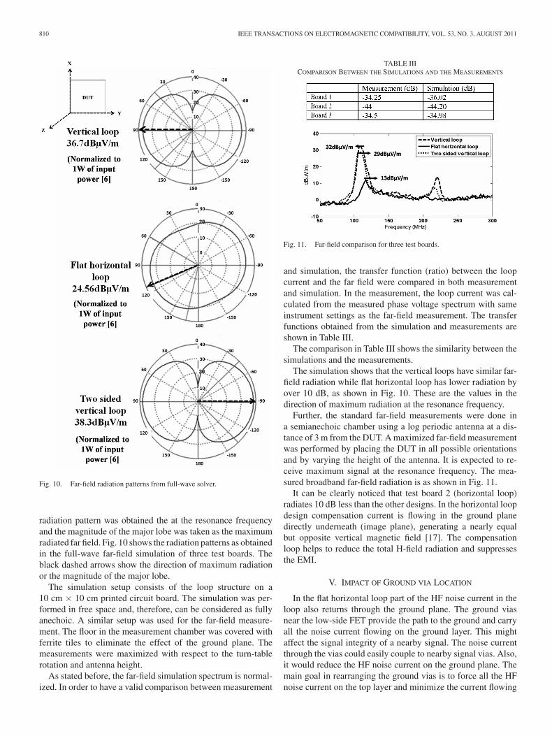
The far field is first verified using full-wave simulations. Thedc feed cable was not considered. During the measurements,we added ferrites to the feed cable and verified that the ca-ble position has no significant influence anymore. A broad-band field monitor was used in a time domain full-wave solver(CST-MWS) to monitor the far-field radiation at a distance of3 m. The radiation pattern at the resonance frequency was ob-tained in dBμV/m and the magnitudes of the major lobe werecompared for all the three test boards. The frequency domainresults in CST Microwave studio are normalized to 1 W of inputpower but the time domain results are not normalized [6].
The three radiation patterns were obtained in the x-y plane inhorizontal polarization and the planes are shown in Fig. 10. The
810 IEEE TRANSACTIONS ON ELECTROMAGNETIC COMPATIBILITY, VOL. 53, NO. 3, AUGUST 2011
Fig. 10. Far-field radiation patterns from full-wave solver.
radiation pattern was obtained the at the resonance frequencyand the magnitude of the major lobe was taken as the maximumradiated far field. Fig. 10 shows the radiation patterns as obtainedin the full-wave far-field simulation of three test boards. Theblack dashed arrows show the direction of maximum radiationor the magnitude of the major lobe.
The simulation setup consists of the loop structure on a10 cm × 10 cm printed circuit board. The simulation was per-formed in free space and, therefore, can be considered as fullyanechoic. A similar setup was used for the far-field measure-ment. The floor in the measurement chamber was covered withferrite tiles to eliminate the effect of the ground plane. Themeasurements were maximized with respect to the turn-tablerotation and antenna height.
As stated before, the far-field simulation spectrum is normal-ized. In order to have a valid comparison between measurement
TABLE IIICOMPARISON BETWEEN THE SIMULATIONS AND THE MEASUREMENTS
Fig. 11. Far-field comparison for three test boards.
and simulation, the transfer function (ratio) between the loopcurrent and the far field were compared in both measurementand simulation. In the measurement, the loop current was cal-culated from the measured phase voltage spectrum with sameinstrument settings as the far-field measurement. The transferfunctions obtained from the simulation and measurements areshown in Table III.
The comparison in Table III shows the similarity between thesimulations and the measurements.
The simulation shows that the vertical loops have similar far-field radiation while flat horizontal loop has lower radiation byover 10 dB, as shown in Fig. 10. These are the values in thedirection of maximum radiation at the resonance frequency.
Further, the standard far-field measurements were done ina semianechoic chamber using a log periodic antenna at a dis-tance of 3 m from the DUT. A maximized far-field measurementwas performed by placing the DUT in all possible orientationsand by varying the height of the antenna. It is expected to re-ceive maximum signal at the resonance frequency. The mea-sured broadband far-field radiation is as shown in Fig. 11.
It can be clearly noticed that test board 2 (horizontal loop)radiates 10 dB less than the other designs. In the horizontal loopdesign compensation current is flowing in the ground planedirectly underneath (image plane), generating a nearly equalbut opposite vertical magnetic field [17]. The compensationloop helps to reduce the total H-field radiation and suppressesthe EMI.
V. IMPACT OF GROUND VIA LOCATION
In the flat horizontal loop part of the HF noise current in theloop also returns through the ground plane. The ground viasnear the low-side FET provide the path to the ground and carryall the noise current flowing on the ground layer. This mightaffect the signal integrity of a nearby signal. The noise currentthrough the vias could easily couple to nearby signal vias. Also,it would reduce the HF noise current on the ground plane. Themain goal in rearranging the ground vias is to force all the HFnoise current on the top layer and minimize the current flowing
BHARGAVA et al.: DC-DC BUCK CONVERTER EMI REDUCTION USING PCB LAYOUT MODIFICATION 811
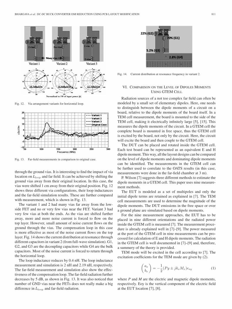
Fig. 12. Via arrangement variants for horizontal loop.
Fig. 13. Far-field measurements in comparison to original case.
through the ground vias. It is interesting to find the impact of vialocation on Lloop and far field. It can be achieved by shifting theground vias away from their original location. In this case, thevias were shifted 1 cm away from their original position. Fig. 12shows three different via configurations, their loop inductancesand the far-field simulation results. These are further comparedwith measurement, which is shown in Fig. 13.
The variant 1 and 2 had many vias far away from the low-side FET and no or very few vias near the FET. Variant 3 hadvery few vias at both the ends. As the vias are shifted furtheraway, more and more noise current is forced to flow on thetop layer. However, small amount of noise current flows on theground through the vias. The compensation loop in this caseis more effective as most of the noise current flows on the toplayer. Fig. 14 shows the current distribution at resonance throughdifferent capacitors in variant 2 (from full-wave simulation). G1,G2, and G3 are the decoupling capacitors while G4 are the bulkcapacitors. Most of the noise current is forced to return throughthe horizontal loop.
The loop inductance reduces by 0.4 nH. The loop inductancemeasurement and simulation is 2 nH and 2.19 nH, respectively.The far-field measurement and simulation also show the effec-tiveness of the compensation loop. The far-field radiation furtherdecreases by 5 dB, as shown in Fig. 13. It was also noticed thatnumber of GND vias near the FETs does not really make a bigdifference in Lloop and far-field radiation.
Fig. 14. Current distribution at resonance frequency in variant 2.
VI. COMPARISON ON THE LEVEL OF DIPOLES MOMENTS
USING GTEM CELL
Radiation sources of a not too complex far field can often bemodeled by a small set of elementary dipoles. Here, one needsto distinguish between the dipole moments of a circuit on aboard, relative to the dipole moments of the board itself. In aTEM cell measurement, the board is mounted to the side of theTEM cell, making it electrically infinitely large [5], [15]. Thismeasures the dipole moments of the circuit. In a GTEM cell thecomplete board is mounted in free space, thus the GTEM cellis excited by the board, not only by the circuit. Here, the circuitwill excite the board and then couple to the GTEM cell.
The DUT can be placed and rotated inside the GTEM cell.Each test board can be represented as an equivalent E and Hdipole moment. This way, all the layout designs can be comparedon the level of dipole moments and dominating dipole momentscan be identified. The measurements in the GTEM cell canbe further used to correlate to the OATS results (in this case,measurements were done in the far-field chamber at 3 m).
P. Wilson [7] suggests three different methods to estimate thedipole moments in a GTEM cell. This paper uses nine measure-ment methods.
The EUT is modeled as a set of multipoles and only theinitial dipole terms are retained as explained in [7]. The TEMcell measurements are used to determine the magnitude of thedipole moments. The DUT emissions in the free space or overa ground plane are simulated based on dipole moments.
For the nine measurement approaches, the EUT has to beplaced in nine different orientations and the radiated powerinside the GTEM cell is measured [7]. The measurement proce-dure is already explained well in [7]–[9]. The power measuredat the port of the GTEM cell in nine measurements can be pro-cessed for calculation of E and H dipole moments. The radiationin the GTEM cell is well documented in [7]–[9] and, therefore,a summery of the theory is provided.
TEM mode will be excited in the cell according to [7]. Theexcitation coefficients for the TEM mode are given by (2).
(ao
bo
)= −1
2(Py ± jkoMx)eoy (1)
where P and M are the electric and magnetic dipole moments,respectively. Eoy is the vertical component of the electric fieldat the EUT location [7], [8].
812 IEEE TRANSACTIONS ON ELECTROMAGNETIC COMPATIBILITY, VOL. 53, NO. 3, AUGUST 2011
TABLE IVVECTOR ADDITION OF CALCULATED VALUE OF E AND H DIPOLE MOMENTS
ALONG EACH AXIS FOR THE THREE MAIN TEST BOARDS WITH DIFFERENT
LOOP ORIENTATIONS
The measured power at the GTEM cell port is normalized by(1/4)e2
oy . |ao |2 and |bo |2 are the powers carried at the port ofthe GTEM cell [8]. The normalized power at the port is givenby (3) [7].
|bo(α)|2 = P 2y + k2
oM 2x . (2)
The nine measurements can be related to the electric and mag-netic dipoles along x, y, and z axis using (2). Therefore, ninedifferent equations are obtained. These equations can be solvedsimultaneously to obtain the values of Px, Py, Pz, Mx, My, andMz as a function of frequency [7]. Once all the six unknownsare obtained, the vector magnitude of electric dipole moment Pand magnetic dipole moment M can be found from (3).
P =√
P 2x + P 2
y + P 2z
M =√
M 2x + M 2
y + M 2z . (3)
Table IV shows the vector addition of calculated valued of Eand H dipole moments along each axis for the three main testboards with different loop orientations.
It is to be noted that P and koM have the same units and, there-fore, they can be directly compared [7]. The magnetic dipolemoments of the vertical loops are about three times strongerthan the flat horizontal loop.
Maximum far-field strength can be predicted from the radi-ated power inside a GTEM cell. According to [7], the powermeasured in the three basic positions can be used to predict themaximized far-field strength using (4).
Po = 10k2o (b11 + b22 + b33) (4)
where b11 , b22 , b33 are the powers measured at the GTEM cellport in three basic orientations.
The electric field in the far-field (at a distance r) due to a shortdipole is given by (5) [7].
Eθ = 30
√Po
10(sin θ)
e−jkr
r. (5)
We assume that the total power radiated is due to a short dipolemoment and is represented by the measurements in a GTEMcell. This is a good representation if the single dipole moment isdominant. Now, this dipole is located over a ground screen andvertical and horizontal electric fields are calculated. It shouldbe noted that the geometry factors in (6) and (7) have to be
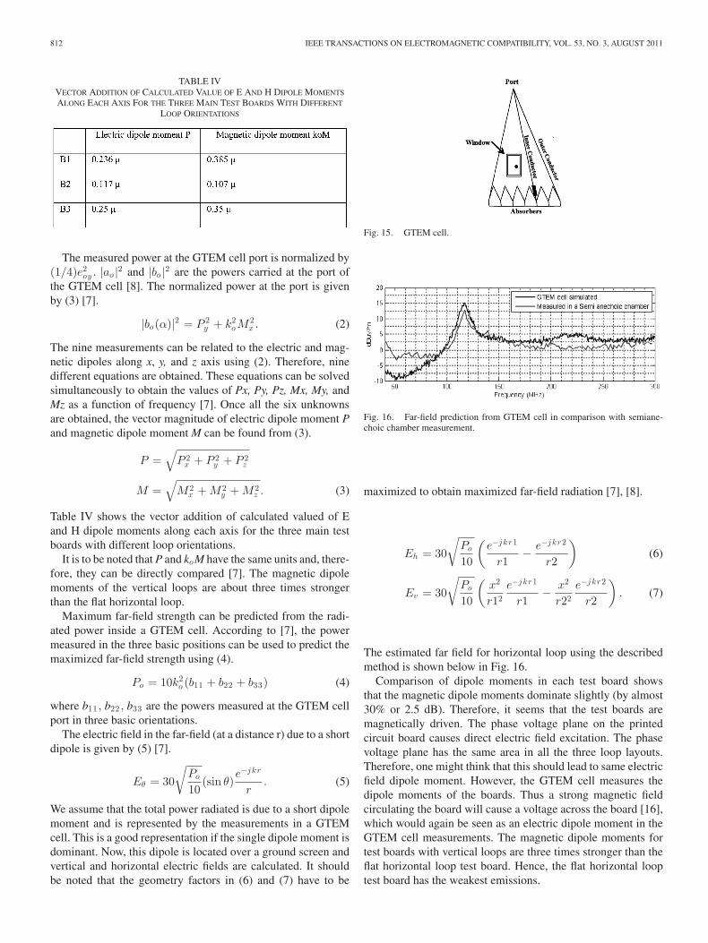
Fig. 15. GTEM cell.
Fig. 16. Far-field prediction from GTEM cell in comparison with semiane-choic chamber measurement.
maximized to obtain maximized far-field radiation [7], [8].
Eh = 30
√Po
10
(e−jkr1
r1− e−jkr2
r2
)(6)
Ev = 30
√Po
10
(x2
r12
e−jkr1
r1− x2
r22
e−jkr2
r2
). (7)
The estimated far field for horizontal loop using the describedmethod is shown below in Fig. 16.
Comparison of dipole moments in each test board showsthat the magnetic dipole moments dominate slightly (by almost30% or 2.5 dB). Therefore, it seems that the test boards aremagnetically driven. The phase voltage plane on the printedcircuit board causes direct electric field excitation. The phasevoltage plane has the same area in all the three loop layouts.Therefore, one might think that this should lead to same electricfield dipole moment. However, the GTEM cell measures thedipole moments of the boards. Thus a strong magnetic fieldcirculating the board will cause a voltage across the board [16],which would again be seen as an electric dipole moment in theGTEM cell measurements. The magnetic dipole moments fortest boards with vertical loops are three times stronger than theflat horizontal loop test board. Hence, the flat horizontal looptest board has the weakest emissions.
BHARGAVA et al.: DC-DC BUCK CONVERTER EMI REDUCTION USING PCB LAYOUT MODIFICATION 813
VII. CONCLUSION
This article suggested several dc-dc synchronous buck con-verter PCB layout modifications, which proved to be very ef-fective in mitigation of the EMI problem. The parasitic loopinductance and the radiated emissions have been minimized bycareful optimization of the PCB layout design. It was provedthat a flat horizontal loop over a ground plane has the lowestradiated emissions. Also, the flat horizontal loop has very largearea but a similar loop inductance as the vertical loops. The ra-diated emissions can be further suppressed by forcing the noisecurrents to stay in the horizontal loop.
In the end, a GTEM cell was used to model each test boardas an equivalent E and H dipole moment. The test boards seemto be magnetically driven. The magnetic dipole moment of flathorizontal test board is the weakest, leading to weaker radiatedemissions.
REFERENCES
[1] A. Bhargava, D. Pommereneke, and K. Kam, “EMI Prediction in switchedpower supplies by full-wave and non-linear circuit co-simulation,” in Proc.IEEE Int. Symp. Electromagn. Compat. Austin, TX, 17–21 Aug. 2009,pp. 41–46.
[2] K. W. Kam and D. Pommerenke, “EMI analysis methods for synchronousbuck converter EMI root cause analysis,” in Proc. IEEE Int. Symp. Elec-tromagn. Compat. Detroit, MI, 18–22 Aug. 2008, pp. 1–7.
[3] K. Kam and D. Pommerenke, “EMC guideline for synchronous buck con-verter design,” in Proc. IEEE Int. Symp. Electromagn. Compat. Austin,TX, 17–21 Aug. 2009, pp. 47–52.
[4] J. R. Warren, K. A. Rosowski, and D. J. Perreault, “Selection and design ofa VHF DC-DC power converter,” IEEE Trans. Power Electron., vol. 23,no. 1, pp. 27–37, Jan. 2008.
[5] S. Deng, “Innovative applications of TEM cell measurements in predictingradiated emission due to common-mode current on printed circuit boards,”Ph.D. dissertation, Dept. Electr. Eng., Univ. of Missouri – Rolla, 2007.
[7] P. Wilson, “On correlating TEM cell and OATS Enission measurements,”IEEE Trans. Electromagn. Compat., vol. EMC-37, no. 1, pp. 1–16, Feb.1995.
[8] A. Nothofer and A. C. Marvin, “Aspects of GTEM to OATS measurementcorrelation,” in Proc. Int. Conf. Electromagn. Compat.. Coventry, U.K,1–3 Sep. 1997, pp. 170–174.
[9] A. K. Lee, “An advanced correlation algorithm between GTEM and OATSfor radiated emission tests,” ETRI J., vol. 17, no. 3, pp. 45–63, Oct. 1995.
[10] K. Harada and T. Ninomiya, “Optimum design of RC snubbers for switch-ing regulators,” IEEE Trans. Aerosp. Electron. Syst., vol. AES-15, no. 2,pp. 209–217, Mar. 1979.
[11] C. U-Yaisom, W. Khanngern, and S. Nitta, “The study and analysis of theconducted EMI suppression on power MOSFET using passive snubbercircuits,” in Proc. 3rd Int. Symp. Electromagn. Compat., 2002, 21–24May, 2002, pp. 561–564.
[12] M. H. Rashid, “Switched power supplies,” in Power Electronics Hand-book. London, U.K: Academic Press, 2001, pp. 211–223.
[13] Z. Li and D. Pommerenke, “EMI specifics of synchronous DC-DC buckconverters,” in Proc. 2005 Int. Symp. Electromagn. Compat., 8–12 Aug.,2005, vol. 3, pp. 711–714.
[14] K. Kam, A. Bhargava, and D. Pommerenke, “Quantification of self damp-ing of power MOSFET in synchronous buck converter,” unpublished.
[15] S. Deng, T. H. Hubing, and D. Beetner, “Using TEM cell measurementsto estimate the maximum radiation from PCBs with cables due to mag-netic field coupling,” IEEE Trans. Electromagn. Compat., vol. 50, no. 2,pp. 419–423, May 2008.
[16] T. Hubing, “Printed circuit boards emi source mechanisms,” in Proc. 2003IEEE Int. Symp. Electromagn. Compat., 18–22 Aug. 2003, vol. 1, pp. 1–3.
[17] J. T. Fessler, K. W. Whites, and C. R. Paul, “The effectiveness of animage plane in reducing radiated emissions,” IEEE Trans. Electromagn.Compat., vol. 38, no. 1, pp. 51–61, Feb. 1996.
Ankit Bhargava (M’05) was born in India, in 1985.He received the B.S.E.E degree in electronics andcommunication engineering, in 2007, from the Uni-versity of Nagpur – India, and the Master’s degree inelectrical engineering from EMC Laboratory of theUniversity of Missouri – Rolla, which is now Mis-souri University of Science and Technology.
He is currently working with Research in Motion,Chicago, IL, as a Power Design Engineer, focusingon full power design for low power handheld design,current drain, and battery and power management.
His research interests include EMI in switched power supplies, cosimulations(full-wave + SPICE), RF system design, and power design.
David Pommerenke (SM’03) received the Ph.D. de-gree from the Technical University Berlin, Germany,in 1996.
After working at Hewlett Packard for 5 years,he joined the Electromagnetic Compatibility Labora-tory at the University Missouri Rolla, MO, in 2001,where he is a Tenured Professor now. His researchinterests include system level ESD, numerical simu-lations, EMC measurement methods, and instrumen-tations. He has published more than 100 papers andis inventor on 10 patents.
Prof. Pommerenke has been a Distinguished Lecturer for the IEEE EMCSociety during 2006–2007.
Keong W. Kam (M’07) was born in South Korea,in 1986. He received the B.S.E.E degree in electricalengineering, in 2007, from the University of Mis-souri – Rolla, MO, which is now Missouri Universityof Science and Technology. He is currently pursu-ing the Ph.D. degree in electrical engineering fromEMC Laboratory at Missouri University of Scienceand Technology.
For the summers of 2008, 2009, and 2010, hewas at Apple Product EMC Group as a Summer In-tern working on projects related to EMC of switched
dc-dc converters and high-speed I/O connectors. His current research interestincludes EMC of switched power converters, intra-system RF interference, andRF system design.
Federico Centola received the Laurea degree from the Universita’ degli Studidi L’Aquila, Italy, in 2001, and the M.S. degree from the Missouri Universityof Science and Technology (formerly known as University of Missouri Rolla),Rolla, MO, in 2003, both in electrical engineering.
He is currently an EMC Technologist at Apple Inc., Cupertino, CA. From2003 to 2008, he was an Electromagnetic Application Engineer for FlomericsInc. (later acquired by CST). His research interest includes full wave numericalsimulations, and electrostatic discharge and shielding.
Cheung-Wei Lam received the B.S. degree in electronics from the ChineseUniversity of Hong Kong, Shatin, Hong Kong, in 1987, and the S.M. and Ph.D.degrees in electrical engineering and computer science from the MassachusettsInstitute of Technology, Cambridge, MA, in 1989 and 1993, respectively.
He is currently the Chief EMC Technologist at Apple Inc., Cupertino, CA.Prior to joining Apple, he was a Cofounder and Principal Engineer at Tran-scendent Design Technology and, earlier, a Principal Engineer at Viewlogic’sAdvanced Development Group (formerly Quad Design Technology). From1988 to 1993, he was with the MIT Research Laboratory of Electronics, wherehis focus was on modeling of high-speed interconnects and superconductingtransmission lines. He has authored or presented numerous technical papersand presentations on electromagnetic compatibility and signal integrity relatedsubjects in the US, in Europe, and in Asia. His research interests include boardand system level design and analysis for electromagnetic compatibility, radiofrequency interference, and signal integrity.
Dr. Lam was a corecipient of the Best Paper Award at the 1996 IEEE Interna-tional Symposium on Electromagnetic Compatibility. He is a past IEEE EMCSociety Distinguished Lecturer and currently serves in the IEEE EMC SocietyRespected Speakers Bureau. He has also served on the IEEE EMC SocietyTC-9 Computational Electromagnetics Committee, the IEEE EMC SocietyTC-10 Signal Integrity committee, and the SAE EMC Modeling Task ForceCommittee.