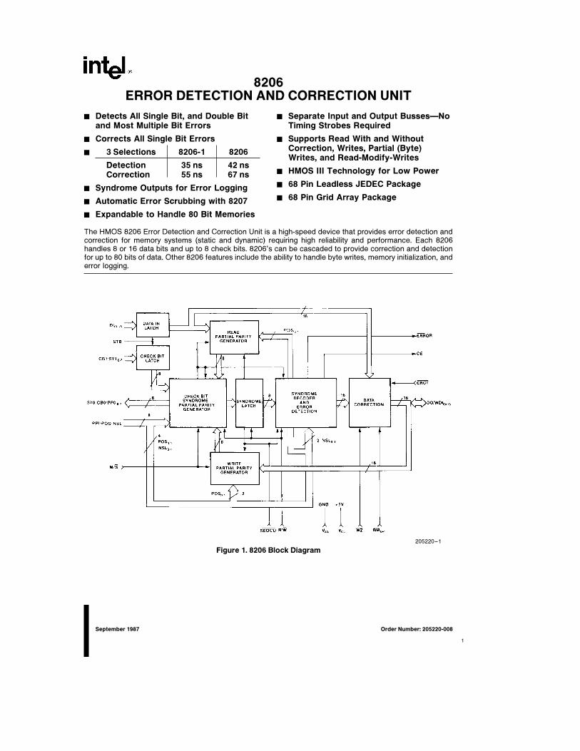
September 1987 Order Number: 205220-008 8206 ERROR DETECTION AND CORRECTION UNIT Y Detects All Single Bit, and Double Bit and Most Multiple Bit Errors Y Corrects All Single Bit Errors Y 3 Selections 8206-1 8206 Detection 35 ns 42 ns Correction 55 ns 67 ns Y Syndrome Outputs for Error Logging Y Automatic Error Scrubbing with 8207 Y Expandable to Handle 80 Bit Memories Y Separate Input and Output Busses—No Timing Strobes Required Y Supports Read With and Without Correction, Writes, Partial (Byte) Writes, and Read-Modify-Writes Y HMOS III Technology for Low Power Y 68 Pin Leadless JEDEC Package Y 68 Pin Grid Array Package The HMOS 8206 Error Detection and Correction Unit is a high-speed device that provides error detection and correction for memory systems (static and dynamic) requiring high reliability and performance. Each 8206 handles 8 or 16 data bits and up to 8 check bits. 8206’s can be cascaded to provide correction and detection for up to 80 bits of data. Other 8206 features include the ability to handle byte writes, memory initialization, and error logging. 205220–1 Figure 1. 8206 Block Diagram 1
Transcript
September 1987 Order Number: 205220-008
8206ERROR DETECTION AND CORRECTION UNIT
Y Detects All Single Bit, and Double Bitand Most Multiple Bit Errors
Y Corrects All Single Bit Errors
Y 3 Selections 8206-1 8206
Detection 35 ns 42 nsCorrection 55 ns 67 ns
Y Syndrome Outputs for Error Logging
Y Automatic Error Scrubbing with 8207
Y Expandable to Handle 80 Bit Memories
Y Separate Input and Output BussesÐNoTiming Strobes Required
Y Supports Read With and WithoutCorrection, Writes, Partial (Byte)Writes, and Read-Modify-Writes
Y HMOS III Technology for Low Power
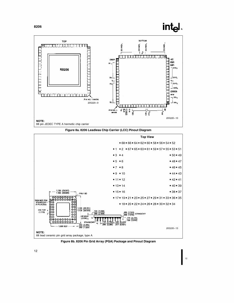
Y 68 Pin Leadless JEDEC Package
Y 68 Pin Grid Array Package
The HMOS 8206 Error Detection and Correction Unit is a high-speed device that provides error detection andcorrection for memory systems (static and dynamic) requiring high reliability and performance. Each 8206handles 8 or 16 data bits and up to 8 check bits. 8206’s can be cascaded to provide correction and detectionfor up to 80 bits of data. Other 8206 features include the ability to handle byte writes, memory initialization, anderror logging.
205220–1
Figure 1. 8206 Block Diagram
1
8206
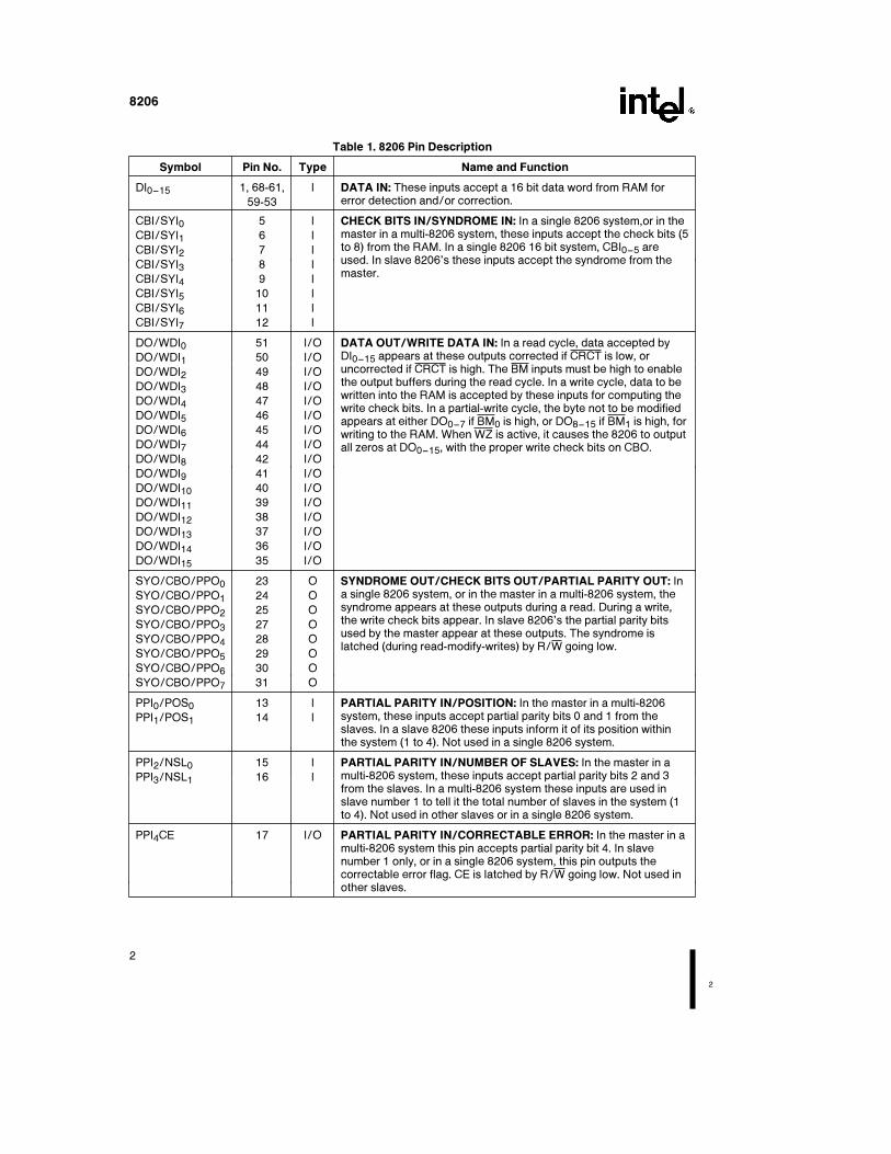
Table 1. 8206 Pin Description
Symbol Pin No. Type Name and Function
DI0–15 1, 68-61, I DATA IN: These inputs accept a 16 bit data word from RAM forerror detection and/or correction.59-53
CBI/SYI0 5 I CHECK BITS IN/SYNDROME IN: In a single 8206 system,or in themaster in a multi-8206 system, these inputs accept the check bits (5CBI/SYI1 6 Ito 8) from the RAM. In a single 8206 16 bit system, CBI0–5 areCBI/SYI2 7 Iused. In slave 8206’s these inputs accept the syndrome from theCBI/SYI3 8 Imaster.
CBI/SYI4 9 I
CBI/SYI5 10 I
CBI/SYI6 11 I
CBI/SYI7 12 I
DO/WDI0 51 I/O DATA OUT/WRITE DATA IN: In a read cycle, data accepted byDI0–15 appears at these outputs corrected if CRCT is low, orDO/WDI1 50 I/Ouncorrected if CRCT is high. The BM inputs must be high to enableDO/WDI2 49 I/Othe output buffers during the read cycle. In a write cycle, data to beDO/WDI3 48 I/Owritten into the RAM is accepted by these inputs for computing the
DO/WDI4 47 I/Owrite check bits. In a partial-write cycle, the byte not to be modified
DO/WDI5 46 I/Oappears at either DO0–7 if BM0 is high, or DO8–15 if BM1 is high, for
DO/WDI6 45 I/O writing to the RAM. When WZ is active, it causes the 8206 to outputDO/WDI7 44 I/O all zeros at DO0–15, with the proper write check bits on CBO.DO/WDI8 42 I/O
DO/WDI9 41 I/O
DO/WDI10 40 I/O
DO/WDI11 39 I/O
DO/WDI12 38 I/O
DO/WDI13 37 I/O
DO/WDI14 36 I/O
DO/WDI15 35 I/O
SYO/CBO/PPO0 23 O SYNDROME OUT/CHECK BITS OUT/PARTIAL PARITY OUT: Ina single 8206 system, or in the master in a multi-8206 system, theSYO/CBO/PPO1 24 Osyndrome appears at these outputs during a read. During a write,SYO/CBO/PPO2 25 Othe write check bits appear. In slave 8206’s the partial parity bitsSYO/CBO/PPO3 27 Oused by the master appear at these outputs. The syndrome is
SYO/CBO/PPO4 28 Olatched (during read-modify-writes) by R/W going low.
SYO/CBO/PPO5 29 O
SYO/CBO/PPO6 30 O
SYO/CBO/PPO7 31 O
PPI0/POS0 13 I PARTIAL PARITY IN/POSITION: In the master in a multi-8206system, these inputs accept partial parity bits 0 and 1 from thePPI1/POS1 14 Islaves. In a slave 8206 these inputs inform it of its position withinthe system (1 to 4). Not used in a single 8206 system.
PPI2/NSL0 15 I PARTIAL PARITY IN/NUMBER OF SLAVES: In the master in amulti-8206 system, these inputs accept partial parity bits 2 and 3PPI3/NSL1 16 Ifrom the slaves. In a multi-8206 system these inputs are used inslave number 1 to tell it the total number of slaves in the system (1to 4). Not used in other slaves or in a single 8206 system.
PPI4CE 17 I/O PARTIAL PARITY IN/CORRECTABLE ERROR: In the master in amulti-8206 system this pin accepts partial parity bit 4. In slavenumber 1 only, or in a single 8206 system, this pin outputs thecorrectable error flag. CE is latched by R/W going low. Not used inother slaves.
2
2
8206
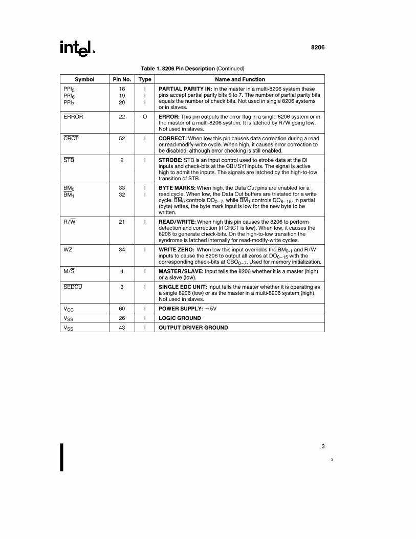
Table 1. 8206 Pin Description (Continued)
Symbol Pin No. Type Name and Function
PPI5 18 I PARTIAL PARITY IN: In the master in a multi-8206 system thesepins accept partial parity bits 5 to 7. The number of partial parity bitsPPI6 19 Iequals the number of check bits. Not used in single 8206 systemsPPI7 20 Ior in slaves.
ERROR 22 O ERROR: This pin outputs the error flag in a single 8206 system or inthe master of a multi-8206 system. It is latched by R/W going low.Not used in slaves.
CRCT 52 I CORRECT: When low this pin causes data correction during a reador read-modify-write cycle. When high, it causes error correction tobe disabled, although error checking is still enabled.
STB 2 I STROBE: STB is an input control used to strobe data at the DIinputs and check-bits at the CBI/SYI inputs. The signal is activehigh to admit the inputs. The signals are latched by the high-to-lowtransition of STB.
BM0 33 I BYTE MARKS: When high, the Data Out pins are enabled for aread cycle. When low, the Data Out buffers are tristated for a writeBM1 32 Icycle. BM0 controls DO0–7, while BM1 controls DO8–15. In partial(byte) writes, the byte mark input is low for the new byte to bewritten.
R/W 21 I READ/WRITE: When high this pin causes the 8206 to performdetection and correction (if CRCT is low). When low, it causes the8206 to generate check-bits. On the high-to-low transition thesyndrome is latched internally for read-modify-write cycles.
WZ 34 I WRITE ZERO: When low this input overrides the BM0-1 and R/Winputs to cause the 8206 to output all zeros at DO0–15 with thecorresponding check-bits at CBO0–7. Used for memory initialization.
M/S 4 I MASTER/SLAVE: Input tells the 8206 whether it is a master (high)or a slave (low).
SEDCU 3 I SINGLE EDC UNIT: Input tells the master whether it is operating asa single 8206 (low) or as the master in a multi-8206 system (high).Not used in slaves.
VCC 60 I POWER SUPPLY: a5V
VSS 26 I LOGIC GROUND
VSS 43 I OUTPUT DRIVER GROUND
3
3
8206
FUNCTIONAL DESCRIPTION
The 8206 Error Detection and Correction Unit pro-vides greater memory system reliability through itsability to detect and correct memory errors. It is asingle chip device that can detect and correct allsingle bit errors and detect all double bit and somehigher multiple bit errors. Some other odd multiplebit errors (e.g., 5 bits in error) are interpreted as sin-gle bit errors, and the CE flag is raised. While someeven multiple bit errors (e.g., 4 bits in error) are inter-preted as no error, most are detected as double biterrors. This error handling is a function of the num-ber of check bits used by the 8206 (see Figure 2)and the specific Hamming code used. Errors incheck bits are not distinguished from errors in aword.
For more information on error correction codes, seeIntel Application Notes AP-46 and AP-73.
A single 8206 handles 8 or 16 bits of data, and up to5 8206’s can be cascaded in order to handle datapaths of 80 bits. For a single 8206 8 bit system, theDI8–15, DO/WDI8–15 and BM1 inputs are grounded.See the Multi-Chip systems section for informationon 24-80 bit systems.
The 8206 has a ‘‘flow through’’ architecture. It sup-ports two kinds of error correction architecture: 1)Flow-through, or correct-always; and 2) Parallel, orcheck-only. These are two separate 16-pin busses,
Data Word Bits Check Bits
8 5
16 6
24 6
32 7
40 7
48 8
56 8
64 8
72 8
80 8
Figure 3. Number of Check Bits Used by 8206
one to accept data from the RAM (DI) and the otherto deliver corrected data to the system bus (DO/WDI). The logic is entirely combinatorial during aread cycle. This is in contrast to an architecture withonly one bus, with bidirectional bus drivers that mustfirst read the data and then be turned around to out-put the corrected data. The latter architecture typi-cally requires additional hardware (latches and/ortransceivers) and may be slower in a system due totiming skews of control signals.
READ CYCLE
With the R/W pin high, data is received from theRAM outputs into the DI pins where it is optionallylatched by the STB signal. Check bits are generatedfrom the data bits and compared to the check bitsread from the RAM into the CBI pins. If an error isdetected the ERROR flag is activated and the cor-rectable error flag (CE) is used to inform the systemwhether the error was correctable or not. With theBM inputs high, the word appears corrected at theDO pins if the error was correctable, or unmodified ifthe error was uncorrectable.
If more than one 8206 is being used, then the checkbits are read by the master. The slaves generate apartial parity output (PPO) and pass it to the master.The master 8206 then generates and returns thesyndrome to the slaves (SYO) for correction of thedata.
The 8206 may alternatively be used in a ‘‘check-only’’ mode with the CRCT pin left high. With thecorrection facility turned off, the propagation delayfrom memory outputs to 8206 outputs is significantlyshortened. In this mode the 8206 issues an ERRORflag to the CPU, which can then perform one of sev-eral options: lengthen the current cycle for correc-tion, restart the instruction, perform a diagnostic rou-tine, etc.
A syndrome word, five to eight bits in length andcontaining all necessary information about the exis-tence and location of an error, is made available tothe system at the SYO0–7 pins. Error logging may beaccomplished by latching the syndrome and thememory address of the word in error.
WRITE CYCLE
For a full write, in which an entire word is written tomemory, the data is written directly to the RAM, by-passing the 8206. The same data enters the 8206through the WDI pins where check bits are generat-ed. The Byte Mark inputs must be low to tristate theDO drivers. The check bits, 5 to 8 in number, arethen written to the RAM through the CBO pins forstorage along with the data word. In a multi-chip sys-tem, the master writes the check bits using partialparity information from the slaves.
In a partial write, part of the data word is overwritten,and part is retained in memory. This is accomplishedby performing a read-modify-write cycle. The com-plete old word is read into the 8206 and corrected,with the syndrome internally latched by R/W goinglow. Only that part of the word not to be modified isoutput onto the DO pins, as controlled by the ByteMark inputs. That portion of the word to be overwrit-
4
4
8206
ten is supplied by the system bus. The 8206 thencalculates check bits for the new word, using thebyte from the previous read and the new byte fromthe system bus, and writes them to the memory.
READ-MODIFY-WRITE CYCLES
Upon detection of an error the 8206 may be used tocorrect the bit in error in memory. This reduces theprobability of getting multiple-bit errors in subse-quent read cycles. This correction is handled by exe-cuting read-modify-write cycles.
The read-modify-write cycle is controlled by the R/Winput. After (during) the read cycle, the system dy-namic RAM controller or CPU examines the 8206ERROR and CE outputs to determine if a correct-able error occurred. If it did, the dynamic RAM con-troller or CPU forces R/W low, telling the 8206 tolatch the generated syndrome and drive the correct-ed check bits onto the CBO outputs. The correcteddata is available on the DO pins. The DRAM control-ler then writes the corrected data and correspondingcheck bits into memory.
The 8206 may be used to perform read-modify-writes in one or two RAM cycles. If it is done in twocycles, the 8206 latches are used to hold the dataand check bits from the read cycle to be used in thefollowing write cycle. The Intel 8207 Dual Port Dy-namic RAM controller allows read-modify-write cy-cles in one memory cycle. See the System Environ-ment section.
INITIALIZATION
A memory system operating with ECC requires someform of initialization at system power-up in or-
der to set valid data and check bit information inmemory. The 8206 supports memory initialization bythe write zero function. By activating the WZ pin, the8206 will write a data pattern of zeros and the asso-ciated check bits in the current write cycle. By thuswriting to all memory at power-up, a controller canset memory to valid data and check bits. Massivememory failure, as signified by both data and checkbits all ones or zeros, will be detected as an uncor-rectable error.
MULTI-CHIP SYSTEMS
A single 8206 handles 8 or 16 bits of data and 5 or 6check bits, respectively. Up to 5 8206’s can be cas-caded for 80 bit memories with 8 check bits.
When cascaded, one 8206 operates as a master,and all others as slaves. As an example, during aread cycle in a 32 bit system with one master andone slave, the slave calculates parity on its portionof the wordБ‘partial parity’’Ðand presents it to themaster through the PPO pins. The master combinesthe partial parity from the slave with the parity it cal-culated from its own portion of the word to generatethe syndrome. The syndrome is then returned by themaster to the slave for error correction. In systemswith more than one slave the above description con-tinues to apply, except that the partial parity outputsof the slaves must be XOR’d externally. Figure 4shows the necessary external logic for multi-chipsystems. Write and read-modify-write cycles are car-ried out analogously. See the System Operation sec-tion for multi-chip wiring diagrams.
There are several pins used to define whether the8206 will operate as a master or a slave. Tables 3and 4 illustrate how these pins are tied.
NOTE:Pins 13, 14, 15, 16 have internal pull-up resistors and may be left as N.C. where specified as connecting to a5V.
6
6
8206
Table 4. NSL Pin Assignments for Slave 1
Number of Slaves
Pin 1 2 3 4
PPI2/NSL0 GND a5V GND a5V
PPI3/NSL1 GND GND a5V a5V
The timing specifications for multi-chip systemsmust be calculated to take account of the externalXOR gating in 3, 4 and 5-chip systems. Let tXOR bethe delay for a single external TTL XOR gate. Thenthe following equations show how to calculate therelevant timing parameters for 2-chip (n e0), 3-chip(n e 1), 4-chip (n e 2), and 5-chip (n e 2) systems:
Data-in to corrected data-out (read cycle) e
TDVSV a TPVSV aTSVQV a ntXOR
Data-in to error flag (read cycle) e
TDVSV a TPVEV a ntXOR
Data-in to correctable error flag (read cycle) e
TDVSV a TPVSV a TSVCV a ntXOR
Write data to check-bits valid (full write cycle) e
TQVQV a TPVSV a ntXOR
Data-in to check-bits valid (read-mod-write cycle) e
TDVSV a TPVSV a TSVQV a TQVQV a TPVSV a
2ntXOR
Data-in to check-bits valid (non-correcting read-modify-write cycle) e
TDVQU a TQVQV a TPVSV a ntXOR
HAMMING CODE
The 8206 uses a modified Hamming code which wasoptimized for multi-chip EDCU systems. The code is
such that partial parity is computed by all 8206’s inparallel. No 8206 requires more time for propagationthrough logic levels than any other one, and henceno one device becomes a bottleneck in the parityoperation. However, one or two levels of externalTTL XOR gates are required in systems with three tofive chips. The code appears in Table 5. The checkbits are derived from the table by XORing or XNOR-ing together the bits indicated by ‘X’s in each rowcorresponding to a check bit. For example, check bit0 in the MASTER for data word 1000110101101011will be ‘‘0’’. It should be noted that the 8206 willdetect the gross-error condition of all lows or allhighs.
Error correction is accomplished by identifying thebad bit and inverting it. Table 5 can also be used asan error syndrome table by replacing the ‘X’s with‘1’s. Each column then represents a different syn-drome word, and by locating the column corre-sponding to a particular syndrome the bit to be cor-rected may be identified. If the syndrome cannot belocated then the error cannot be corrected. For ex-ample, if the syndrome word is 00110111, the bit tobe corrected is bit 5 in the slave one data word (bit21).
The syndrome decoding is also summarized in Ta-bles 6 and 7 which can be used for error logging. Byfinding the appropriate syndrome word (starting withbit zero, the least significant bit), the result is either:1) no error; 2) an identified (correctable) single biterror; 3) a double bit error; or 4) a multi-bit uncorrect-able error.
7
7
8206
Table
5.M
odifie
dH
am
min
gC
ode
Check
Bit
Genera
tion
Check
bits
are
genera
ted
by
XO
R’in
g(e
xceptfo
rth
eC
B0
and
CB
1data
bits,w
hic
hare
XN
OR
’ed
inth
eM
aste
r)th
edata
bits
inth
ero
ws
correspondin
gto
the
check
bits.N
ote
there
are
6check
bits
ina
16-b
itsys
tem
,7
ina
32-b
itsys
tem
,and
8in
48-o
r-m
ore
-bit
sys
tem
s.
BY
TE
NU
MB
ER
01
OPER
ATIO
N2
3O
PER
ATIO
NB
ITN
UM
BER
01
23
45
67
01
23
45
67
01
23
45
67
01
23
45
67
CB
0e
xx
-x
-x
x-
x-
-x
-x
--
XN
OR
-x
xx
-x
x-
-x
x-
-x
--
XO
R
CB
1e
x-
x-
-x
-x
-x
-x
x-
x-
XN
OR
xx
x-
-x
-x
xx
--
--
-x
XO
R
CB
2e
-x
x-
x-
xx
--
x-
x-
-x
XO
R-
xx
x-
xx
x-
-x
x-
--
-XO
R
CH
EC
KC
B3
ex
xx
xx
--
-x
xx
--
--
-XO
Rx
x-
-x
-x
xx
--
xx
--
-XO
R
BIT
SC
B4
e-
--
xx
xx
x-
--
--
xx
xXO
Rx
x-
-x
xx
x-
--
-x
-x
-XO
R
CB
5e
--
--
--
--
xx
xx
xx
xx
XO
R-
--
xx
xx
x-
--
--
xx
xXO
R
CB
6e
--
--
--
--
--
--
--
--
XO
R-
--
--
--
-x
xx
xx
xx
xXO
R
CB
7e
--
--
--
--
--
--
--
--
XO
R-
--
--
--
--
--
--
--
-XO
R
DA
TA
BIT
S0
00
00
00
00
01
11
11
11
11
12
22
22
22
22
23
3
01
23
45
67
89
01
23
45
67
89
01
23
45
67
89
01
16
BIT
OR
MA
STER
SLA
VE
Ý1
BY
TE
NU
MB
ER
45
67
89
OPER
ATIO
NB
ITN
UM
BER
01
23
45
67
01
23
45
67
01
23
45
67
01
23
45
67
01
23
45
67
01
23
45
67
CB
0e
xx
-x
-x
x-
x-
-x
-x
--
x-
x-
xx
--
x-
xx
--
x-
-x
xx
-x
x-
-x
x-
-x
--
XO
R
CB
1e
x-
x-
-x
-x
-x
-x
x-
x-
-x
x-
--
xx
xx
x-
--
x-
-x
xx
-x
xx
--
xx
--
--
XO
R
CB
2e
-x
x-
x-
xx
--
x-
x-
-x
-x
xx
-x
x-
-x
x-
-x
--
x-
-x
-x
x-
-x
x-
-x
-x
XO
R
CH
EC
KC
B3
ex
xx
xx
--
-x
xx
--
--
-x
-x
--
xx
-x
x-
-x
x-
--
xx
xx
--
xx
x-
-x
--
-XO
R
BIT
SC
B4
e-
--
xx
xx
x-
--
--
xx
x-
--
xx
xx
x-
--
--
xx
x-
xx
--
-x
xx
xx
--
-x
-XO
R
CB
5e
xx
xx
xx
xx
--
--
--
--
--
--
--
--
xx
xx
xx
xx
x-
xx
xx
-x
--
-x
--
-x
XO
R
CB
6e
xx
xx
xx
xx
--
--
--
--
xx
xx
xx
xx
--
--
--
--
xx
--
xx
xx
--
--
x-
x-
XO
R
CB
7e
--
--
--
--
xx
xx
xx
xx
--
--
--
--
xx
xx
xx
xx
--
--
--
--
xx
xx
xx
xx
XO
R
DA
TA
BIT
S3
33
33
33
34
44
44
44
44
45
55
55
55
55
56
66
66
66
66
67
77
77
77
77
7
23
45
67
89
01
23
45
67
89
01
23
45
67
89
01
23
45
67
89
01
23
45
67
89
SLA
VE
Ý2
SLA
VE
Ý3
SLA
VE
Ý4
8
8
8206
Table 6. 8206 Syndrome Decoding
0 0 1 0 1 0 1 0 1 0 1 0 1 0 1 0 1
Syndrome 1 0 0 1 1 0 0 1 1 0 0 1 1 0 0 1 1
Bits 2 0 0 0 0 1 1 1 1 0 0 0 0 1 1 1 1
7 6 5 4 3 0 0 0 0 0 0 0 0 1 1 1 1 1 1 1 1
0 0 0 0 N CB0 CB1 D CB2 D D 18 CB3 D D 0 D 1 2 D
0 0 0 1 CB4 D D 5 D 6 7 D D D 16 D 4 D D 17
0 0 1 0 CB5 D D 11 D 19 12 D D 8 9 D 10 D D 67
0 0 1 1 D 13 14 D 15 D D 21 20 D D 66 D 22 23 D
0 1 0 0 CB6 D D 25 D 26 49 D D 48 24 D 27 D D 50
0 1 0 1 D 52 55 D 51 D D 70 28 D D 65 D 53 54 D
0 1 1 0 D 29 31 D 64 D D 69 68 D D 32 D 33 34 D
0 1 1 1 30 D D 37 D 38 39 D D 35 71 D 36 D D U
1 0 0 0 CB7 D D 43 D 77 44 D D 40 41 D 42 D D U
1 0 0 1 D 45 46 D 47 D D 74 72 D D U D 73 U D
1 0 1 0 D 59 75 D 79 D D 58 60 D D 56 D U 57 D
1 0 1 1 63 D D 62 D U U D D U U D 61 D D U
1 1 0 0 D U U D U D D U 76 D D U D U U D
1 1 0 1 78 D D U D U U D D U U D U D D U
1 1 1 0 U D D U D U U D D U U D U D D U
1 1 1 1 D U U D U D D U U D D U D U U D
N e No ErrorCBX e Error in Check Bit XX e Error in Data Bit XD e Double Bit ErrorU e Uncorrectable Multi-Bit Error
SYSTEM ENVIRONMENT
The 8206 interface to a typical 32 bit memory sys-tem is illustrated in Figure 5. For larger systems, thepartial parity bits from slaves two to four must beXOR’ed externally, which calls for one level of XORgating for three 8206’s and two levels for four or five8206’s.
The 8206 is designed for direct connection to theIntel 8207 Dynamic RAM Controller. The 8207
has the ability to perform dual port memory control,and Figure 6 illustrates a highly integrated dual portRAM implementation using the 8206 and 8207. The8206/8207 combination permits such features asautomatic scrubbing (correcting errors in memoryduring refresh), extending RAS and CAS timings forRead-Modify-Writes in single memory cycles, andautomatic memory initialization upon reset. Togetherthese two chips provide a complete dual-port, error-corrected dynamic RAM subsystem.
9
9
8206
205220–6
Figure 5. 32-Bit 8206 System Interface
205220–7
Figure 6. Dual Port RAM Subsystem with 8206/8207 (32-bit bus)
10
10
8206
MEMORY BOARD TESTING
The 8206 lends itself to straightforward memoryboard testing with a minimum of hardware overhead.The following is a description of four common testmodes and their implementation.
Mode 0Ð Read and write with error correction.Implementation: This mode is the normal8206 operating mode.
Mode 1Ð Read and write data with error correctiondisabled to allow test of data memory.Implementation: This mode is performedwith CRCT deactivated.
Mode 2Ð Read and write check bits with error cor-rection disabled to allow test of check bitsmemory.
Implementation: Any pattern may be writ-ten into the check bits memory by judi-ciously choosing the proper data word to
generate the desired check bits, throughthe use of the 8206 Hamming code. Toread out the check bits it is first necessaryto fill the data memory with all zeros,which may be done by activating WZ andincrementing memory addresses with WEto the check bits memory held inactive,and then performing ordinary reads. Thecheck bits will then appear directly at theSYO outputs, with bits CB0 and CB1 in-verted.
Mode 3Ð Write data, without altering or writingcheck bits, to allow the storage of bitcombinations to cause error correctionand detection.
Implementation: This mode is implement-ed by writing the desired word to memorywith WE to the check bits array held inac-tive.
Ambient Temperature Under Bias ÀÀÀÀÀÀ0§C to 70§CStorage Temperature ÀÀÀÀÀÀÀÀÀÀb65§C to a150§CVoltage On Any Pin
with Respect to GroundÀÀÀÀÀÀÀÀÀÀb0.5V to a7V
Power DissipationÀÀÀÀÀÀÀÀÀÀÀÀÀÀÀÀÀÀÀÀÀÀÀÀÀÀ1.5W
NOTICE: This is a production data sheet. The specifi-cations are subject to change without notice.
*WARNING: Stressing the device beyond the ‘‘AbsoluteMaximum Ratings’’ may cause permanent damage.These are stress ratings only. Operation beyond the‘‘Operating Conditions’’ is not recommended and ex-tended exposure beyond the ‘‘Operating Conditions’’may affect device reliability.
D.C. CHARACTERISTICS TA e 0§C to 70§C, VCC e 5.0V g 10%, VSS e GND
Symbol Parameter Min Max Units Test Conditions
ICC Power Supply Current
ÐSingle 8206 or 270 mA
Slave Ý1
ÐMaster in Multi-Chip 230 mA
or Slaves Ý2, 3, 4
VIL(1) Input Low Voltage b0.5 0.8 V
VIH(1) Input High Voltage 2.0 VCC a V
0.5V
VOL Output Low Voltage
ÐDO 0.45 V IOL e 8 mA
ÐAll Others 0.45 V IOL e 2.0 mA
VOH Output High Voltage
ÐDO, CBO 2.6 V IOH e b2 mA
ÐAll Other Outputs 2.4 V IOH e b0.4 mA
ILO I/O Leakage Current
ÐPPI4/CE g20 mA 0.45V s VI/O s VCC
ÐDO/WDI0–15 g10 mA
ILI Input Leakage Current
ÐPPI0–3, 5–7, CBI6-7, SEDCU(2) g20 mA 0V s VIN s VCC
ÐAll Other Input Only Pins g10 mA
NOTES:1. SEDCU (pin 3) and M/S (pin 4) are device strapping options and should be tied to VCC or GND. VIH min e VCC b0.5Vand VIL max e 0.5V.2. PPI0–7 (pins 13–20) and CBI6-7 (pins 11, 12) have internal pull-up resistors and if left unconnected will be pulled to VCC.
A.C. TESTING INPUT, OUTPUT WAVEFORM
205220–14A.C. Testing: Inputs are driven at 2.4V for a Logic ‘‘1’’ and 0.45Vfor a Logic ‘‘0’’. Timing measurements are made at 2.0V for aLogic ‘‘1’’ and 0.8V for a Logic ‘‘0’’.
A.C. TESTING LOAD CIRCUIT
205220–15CL Includes Jig Capacitance
13
13
8206
A.C. CHARACTERISTICSTA e 0§C to 70§C, VCC e a5V g 10%, VSS e 0V, RL e 22X, CL e 50 pF; all times are in ns
Symbol Parameter8206-1 8206
NotesMin Max Min Max
TRHEV ERROR Valid from R/Wu 20 25
TRHCV CE Valid from R/Wu (Single 8206) 34 44
TRHQV Corrected Data Valid from RWu 44 54 1
TRVSV SYO/CBO/PPO Valid from R/W 32 42 1
TDVEV ERROR Valid from Data/Check Bits In 35 42
TDVCV CE Valid from Data/Check Bits In 50 70
TDVQV Corrected Data Valid from Data/Check Bits In 55 67
TDVSV SYO/PPO Valid from Data/Check Bits In 40 55
TBHQV Corrected Data Access Time 35 37
TBXQX Hold Time from Data/Check Bits In 0 0 1
TBLQZ Corrected Data Float Delay 0 25 0 28 1
TSHIV STB High to Data/Check Bits In Valid 30 30 2
TIVSL Data/Check Bits In to STBv Set-Up 5 5
TSLIX Data/Check Bits In from STBv Hold 15 25
TPVEV ERROR Valid from Partial Parity In 21 30 3
TPVQV Corrected Data (Master) from Partial Parity In 46 61 1, 3
TPVSV Syndrome/Check Bits Out from Partial Parity In 32 43 1, 3
TSVQV Corrected Data (Slave) Valid from Syndrome 41 51 3
TSVCV CE Valid from Syndrome (Slave Number 1) 43 48 3
TQVQV Check Bits/Partial Parity Out from Write Data In 44 64 1
TRHSX Check Bits/Partial Parity Out from R/W, WZ Hold 0 0 1
TRLSX Syndrome Out from R/W Hold 0 0
TQXQX Hold Time from Write Data In 0 0 1
TSVRL Syndrome Out to R/Wv Set-Up 5 17 3
TDVRL Data/Check Bits to R/W Set-Up 24 39 1
TDVQU Uncorrected Data Out from Data In 29 32
TTVQV Corrected Data Out from CRCTv 25 30
TWLQL WZv to Zero Out 25 30
TWHQX Zero Out from WZu Hold 0 0 0
NOTES:1. A.C. Test Levels for CBO and DO are 2.4V and 0.8V.2. TSHIV is required to guarantee output delay timings: TDVEV, TDVCV, TDVQV, TDVSV, TSHIV a TIVSL guarantees a min STBpulse width of 35 ns.3. Not required for 8/16 bit systems.