24
Revision: C Avalanche Technology Page 1 | 24 8Mbit – 64Mbit Embedded MRAM Macro (eMRAM)

Revision: C A v a l a n c h e T e c h n o l o g y P a g e 1 | 24
8Mbit – 64Mbit
Embedded MRAM Macro
(eMRAM)

Revision: C A v a l a n c h e T e c h n o l o g y P a g e 2 | 24
Purpose The document describes the system level requirements for 8Mbit-64Mbit Embedded MRAM (eMRAM)
macro. It includes the following:
Executive Summary
What’ Available in the Market
Application Space
Market Positioning
Signal Description & Assignment
Bus Interface
Electrical Specifications
Background on Embedded MRAM (eMRAM) eMRAM technology is analogous to embedded Flash (eFlash) technology which is widely used in SoCs.
However, eFlash technology is facing scaling challenges beyond 28/40nm nodes, where endurance and
leakage are making its use prohibitive. eMRAM, on the other hand, scales well since it requires standard
CMOS manufacturing processes with two additional masks. eMRAM being a highly reliable and fast non-
volatile memory, is rapidly becoming the embedded memory choice in SoCs replacing eFlash with an
embedded MRAM memory macro.
Table 1: Technology Comparison
eSRAM eFlash eEEPROM eMRAM
Non-Volatility ↓ ↑ ↑ ↑
Write Performance ↑ ↓ ↓ ↑
Read Performance ↑ − − ↑
Endurance ↑ ↓ ↓ ↑
Power ↓ ↓ − ↑
Cost per Memory Bit ↓ − ↓ ↑
Executive Summary The eMRAM macro is a magneto-resistive random-access memory (MRAM) macro ranging in density from
8Mbit to 64Mbit organized in words (word: 32 bits). The eMRAM offers AMBA AHB-Lite compatible
interface operating up to a maximum of 400MHz.
eMRAM is a true random-access memory; allowing both reads and writes to occur randomly in memory.
The eMRAM is ideal for applications that must store and retrieve data without incurring large latency
penalties. It offers low latency, low power, infinite endurance, high performance and scalable memory
technology.

Revision: C A v a l a n c h e T e c h n o l o g y P a g e 3 | 24
eMRAM Use Model Figure 1 shows a typical SoC with integrated eMRAM macro.
Figure 1: eMRAM Use Model
CPU Subsystem
System Interconnect
System Interconnect
eMRAM8Mb – 64Mb
Control Logic
SWD
Main CPU
System Resources
Digital DFT
Test
Analog DFT
Power
Clock
Reset
Clock ControlIMO
Sleep Control
PWRSYS
REF
POR
Reset Control
TestMode Entry
WIC
Standard Peripherals
PWM
LCD
CO
MPA
RA
TOR
S
CA
PSE
NSE
CA
N
CR
YPTO
(AES
/SH
A/R
NG
)
I2C
/SPI
/UA
RT
High Speed I/O Matrix
High-Speed Peripherals
DMAMMIO
ETH
ERN
ET
DMAMMIO
USB
-HS
CH
G-D
ET
HS/
FS/L
S PH
Y
Eth
ern
et1
0/1
00PH
Y
IO Subsystem
I/O Pins (Digital, High Speed)
System Interconnect
SRAM8KB
Control Logic
Features Interface: AMBA 3 AHB-Lite Protocol
Technology: 28nm MRAM
Density: 8Mbit – 64Mbit
Operating Voltage Range: VCC: 0.80V – 1.05V, 1.7V-2.0V,
Operating Temperature Range (Junction Temperature): -40°C to 125°C
Maximum Clock Speed: 400MHz (maximum)
Read Latency: 10 Clock Cycles (maximum) (25ns)
Write Latency: 80 Clock Cycles (maximum) (200ns)
Endurance: 1x10⁹ Write Cycles

Revision: C A v a l a n c h e T e c h n o l o g y P a g e 4 | 24
Retention: 10 years
Low Power (hibernate Mode): Leakage 5µA (typical)
Supervisory Area: Configuration and Security support
Table 2: Macro Area
Density X Dimension (um)
Y Dimension (um)
Size (mm2)
64Mbit 2,116.08 3,282.16 2.64
32Mbit 2,298.08 1,703.63 1.98
16Mbit 2,296.08 914.36 1.45
8Mbit 1,328.04 914.36 1.10
4Mbit 857.52 914.36 0.89
Performance Table 3: Performance Requirements
Device Operation Values Units
Read (Word: 32 bits)) 25.0 ns
Write (Word: 32 bits) 200.0 ns
Standby 250.0 µA
Hibernate Power Mode 5.0 µA
Read (Word: 32 bits) 5.0 @40MHz mA
Write (Word: 32 bits) 15.0 @20MHz mA
Revision: C A v a l a n c h e T e c h n o l o g y P a g e 5 | 24
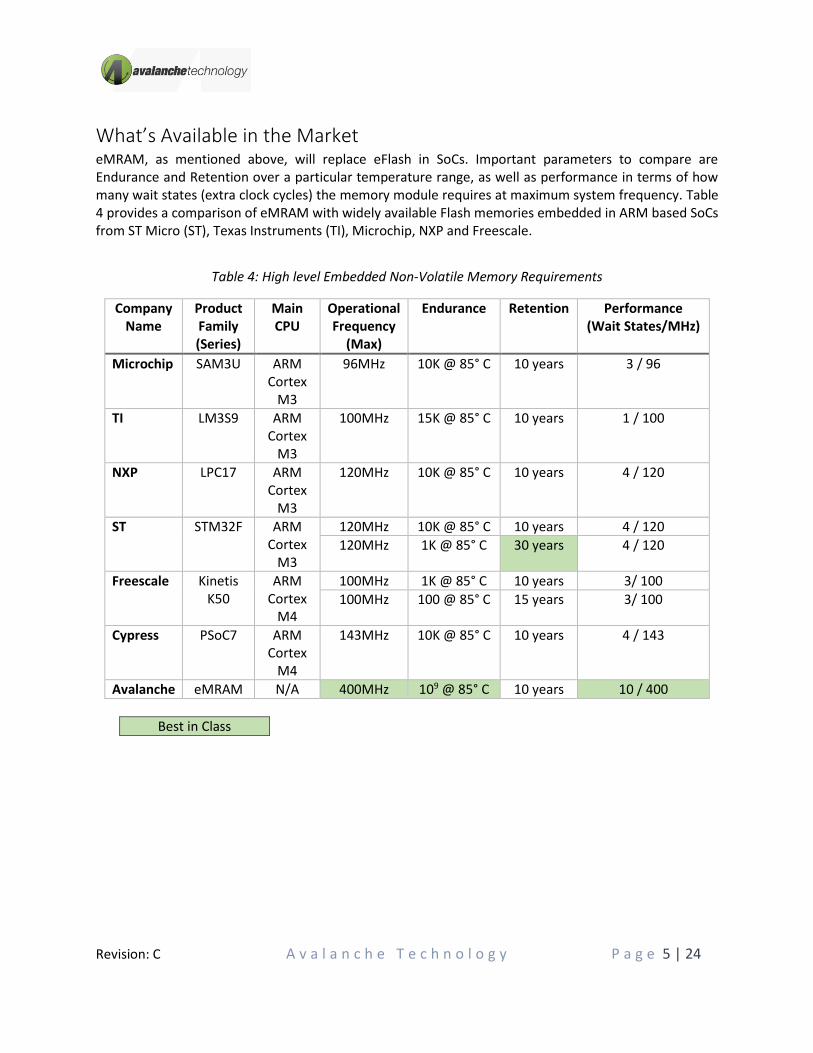
What’s Available in the Market eMRAM, as mentioned above, will replace eFlash in SoCs. Important parameters to compare are Endurance and Retention over a particular temperature range, as well as performance in terms of how many wait states (extra clock cycles) the memory module requires at maximum system frequency. Table 4 provides a comparison of eMRAM with widely available Flash memories embedded in ARM based SoCs from ST Micro (ST), Texas Instruments (TI), Microchip, NXP and Freescale.
Table 4: High level Embedded Non-Volatile Memory Requirements
Company Name
Product Family (Series)
Main CPU
Operational Frequency
(Max)
Endurance Retention Performance (Wait States/MHz)
Microchip SAM3U ARM Cortex
M3
96MHz 10K @ 85° C 10 years 3 / 96
TI LM3S9 ARM Cortex
M3
100MHz 15K @ 85° C 10 years 1 / 100
NXP LPC17 ARM Cortex
M3
120MHz 10K @ 85° C 10 years 4 / 120
ST STM32F ARM Cortex
M3
120MHz 10K @ 85° C 10 years 4 / 120
120MHz 1K @ 85° C 30 years 4 / 120
Freescale Kinetis K50
ARM Cortex
M4
100MHz 1K @ 85° C 10 years 3/ 100
100MHz 100 @ 85° C 15 years 3/ 100
Cypress PSoC7 ARM Cortex
M4
143MHz 10K @ 85° C 10 years 4 / 143
Avalanche eMRAM N/A 400MHz 109 @ 85° C 10 years 10 / 400
Best in Class

Revision: C A v a l a n c h e T e c h n o l o g y P a g e 6 | 24
Application Space Microcontrollers: A microcontroller unit (MCU) is a small computer on a single integrated circuit that typically contains a central processing unit (CPU) core, static random-access memory (SRAM) modules, embedded flash memory modules, a system integration module and peripheral modules including a timer, an analog-to-digital converter (ADC), serial communication and networking. Microcontrollers with embedded flash memories (eFlash) are widely used in real-time control application markets. The programmable code storage provided by on-chip flash memories contributes to the reduction of production costs and expansion of real-time adaptive control applications. Almost all the MCU market segments now use embedded flash solutions. eMRAM is a scalable, high-performance and power-efficient embedded nonvolatile technology. eMRAM is intended to be part of a MCU’s Memory sub-system where it can deliver non-volatile data storage requirements. Although eFlash is largely used for code storage, eMRAM can store both code as well as data for an efficient small-system solution; eMRAM has very high data endurance and data retention limits.

Revision: C A v a l a n c h e T e c h n o l o g y P a g e 7 | 24
Marketing Positioning The major advantages of eMRAM are as follows:
High-performance: eMRAM supports a 32-bit AMBA 3 AHB-Lite interface operating at 400MHz with 4 wait states (read). This translates into 32-bits of data every 10ns (random); 400MB/s sustained throughput is achieved (not a burst throughput). Low Power: Low power mode is required in MCUs running real-time adaptive control applications. Most MCUs spend much of their time in lowered-power states where they are either running from a lowered frequency clock or are in a state where the CPU is suspended with peripherals operating or in a state where all operations are ceased awaiting a resume command based on certain user-selected input; typically, an interrupt or a timer event. eMRAM module supports a low power mode where the macro’s leakage current is 100nA or less. The wakeup time from this low power mode is rapid; less than 1µs. Data Security: eMRAM provides protection against read and write. The protection is address range based and is selected through configuration register setting. If selected, the protection is enabled at power-up and a 256-bit password is required to disable it. As mentioned above, a configuration register implements the protection type (read, write or read and write), the address range, and the 256-bit password.
Write protection: 4 configuration bits selects the protection range – from all to none. Each configuration combination protects 1/16th of the address space. Following is the protection map:
Table 5: Write Protection
Bit Combination Protection
0000 None
0001 1/16th protected starting from address 0
0010 2/16th protected starting from address 0
0011 3/16th protected starting from address 0
0100 4/16th protected starting from address 0
…….
1111 16/16th protected starting from address 0
Read protection: 4 configuration bits select the protection range – none to all. Each configuration combination protects 1/16th of the address space. Following is the protection map: Note: The last 1/16th of the address starting from address 0 is never read protected. This is to ensure there is enough space for basic CPU booting.

Revision: C A v a l a n c h e T e c h n o l o g y P a g e 8 | 24
Table 6: Read Protection
Bit Combination Protection
0000 None
0001 1/16th protected starting from address 0
0010 2/16th protected starting from address 0
0011 3/16th protected starting from address 0
0100 4/16th protected starting from address 0
…….
1110 15/16th protected starting from address 0
1111 Not used

Revision: C A v a l a n c h e T e c h n o l o g y P a g e 9 | 24
Signal Description and Assignment Figure 2: Macro Pinout
8-64Mb
eMRAMMacro
HSEL
HCLK
HRESETn
HADDR[31:0]
HWRITE
HWDATA[31:0]
HREADY
HRDATA[31:0]
HBURST[2:0]
HTRANS[1:0]
HSIZE[2:0]
HRESP
Table 7: Signal Description
Signal Type Description
HSEL Input MRAM SELECTOR: Enables or disables the MRAM macro.
HCLK Input MRAM Clock Source: The bus clock times all bus transfers. All signal timings are
related to the rising edge of HCLK.
HRESETn Input MRAM Reset Controller: The bus reset signal is active LOW and resets the MRAM
macro and brings it into Standby state.
HADDR[31:0] Input MRAM Address Bus: The 32-bit address bus.
HWRITE Input
MRAM Read / Write enable: Indicates the transfer direction. When HIGH this signal
indicates a write transfer and when LOW a read transfer. It has the same timing as the address signals, however, it must remain constant throughout a burst transfer.
HWDATA[31:0] Input MRAM Write Data Bus: The write data bus transfers data from the master to the
MRAM during write operations. The data bus width is 32 bits.
HREADY Output MRAM Ready/Busy: When HIGH, the HREADY signal indicates that a transfer has
finished on the bus. This signal can be driven LOW to extend a transfer.
HRDATA[31:0] Output MRAM Read Data Bus: During read operations, the read data bus transfers data
from the MRAM to the master. The data bus width is 32 bits.
HBURST[2:0] Input
MRAM Burst Type: The burst type indicates if the transfer is a single transfer or
forms part of a burst. Fixed length bursts of 4, 8, and 16 beats are supported. Also, incrementing bursts of undefined length are supported. Note: Wrapped burst is not supported.
HSIZE[2:0] Input MRAM Transfer Size: Indicates the size of the data transfer; byte, half word or word.
HTRANS[1:0] Input MRAM Transfer Type: Indicates the type of transfer; IDLE, BUSY,
NONSEQUENTIAL, SEQUENTIAL.
HRESP Output MRAM TRANSFER STATUS: Provides status on the transfer; whether the transfer
was successful or with errors.
VCC Supply VCC: MRAM macro power supply.
VSS Supply VSS: MRAM macro ground supply.

Revision: C A v a l a n c h e T e c h n o l o g y P a g e 10 | 24
Macro Architecture The eMRAM macro’s internal architecture is shown in Figure 3:
Figure 3: eMRAM Architecture
MRAM
Array
(32k x 32)
MRAM
Array
(32k x 32)
MRAM
Array
(32k x 32)
MRAM
Array
(32k x 32)
MRAM
Array
(32k x 32)
MRAM
Array
(32k x 32)
MRAM
Array
(32k x 32)Control
HADDR[31:0]
HCLK
HRESTn
HWRITE
HSEL
MRAM
Array
(32k x 32)
Ro
w D
ec
od
er
Column
Decoder
Data Buffer
(256 bits)ECC
Data
&
Address
Address Register
Ready / BusyHREADY
HRDATA[31:0]
HWDATA[31:0]
(8)
8 MegabitMacro
(example)
HRESP
HBURST[2:0]
HTRANS[1:0]
HSIZE[2:0]
As can be seen, each eMRAM’s memory array (irrespective of density) is organized in a group of 8 planes.
The example shown depicts an 8Mbit implementation where each plane consists of 1Mbit MRAM cells.
Having this architecture allows every access (reads/write) to generate 256 bits of data maximizing
throughput. These 256 bits of data are then multiplexed to 32-bit outputs/inputs based on the address
provided.
Read The 8-plane architecture maximizes throughput for sequential reads. After providing the initial address
followed by a 4-cycle latency, sequential data can be output at full clock frequency (400MHz) without
incurring any further inter-address latencies. On the other hand, if random reads are required, each new
address will incur a 4-cycles latency.
Write The 8-plane architecture maximizes throughput for sequential writes. The eMRAM macro accepts up to a
maximum of 256 bits (8 sequential address) for each write.

Revision: C A v a l a n c h e T e c h n o l o g y P a g e 11 | 24
Bus Interface As mentioned above, eMRAM supports the AMBA 3 AHB-Lite protocol for read and write operations. Each AHB-Lite transfer consists of two phases:
1. Address Phase: Address phase generally lasts for a single HCLK cycle - unless extended by the previous bus transfer.
2. Data Phase: Data phase can require several HCLK cycles. MRAM uses HREADY signal to control the number of clock cycles required to complete the transfer.
HWRITE controls the direction of data transfer to or from the master. It is based on the following:
HWRITE HIGH (Logic ‘1’) indicates a write transfer and the master transfers data on the write data bus, HWDATA[31:0]
HWRITE LOW (Logic ‘0’) indicates a read transfer and the MRAM generates the data on the read data bus, HRDATA[31:0].
Write Transfer During a Write transfer, the master drives the address and control signals onto the bus. MARM then samples the address and control information on the rising edge of HCLK. After MRAM has sampled the address and control, the master can start to drive the data on the data bus HWDATA[31:0]. In response, MRAM can drive the HREADY which the master samples on the rising edge of HCLK.

Revision: C A v a l a n c h e T e c h n o l o g y P a g e 12 | 24
Figure 4: Write Transfer
t HC
LK
Add
ress
A
t HA
DD
RS
t HA
DD
RH
t CM
DS
Ad
dres
s Ph
ase
HC
LK
HA
DD
R[3
1:0
]
HW
RIT
E
HW
DA
TA[3
1:0
]
HR
EAD
Y
Do
n t
Ca
reD
atai
n P
has
e
t HR
EAD
Y
Dat
a A
+1D
ata
A+6
Dat
a A
t HW
DA
TAS
t HW
DA
TAH
Dat
a A
+7
Add
ress
A+1
t HA
DD
RS
t HA
DD
RH
Add
ress
A+2
t HA
DD
RS
t HA
DD
RH
Add
ress
B
t HA
DD
RS
t HA
DD
RH
t HA
DD
RS
Add
ress
A+7
Dat
a B
t HW
DA
TAS
t HW
DA
TAH
Add
ress
B+1
t HR
EAD
Y

Revision: C A v a l a n c h e T e c h n o l o g y P a g e 13 | 24
Read Transfer During a Read transfer, the master drives the address and control signals onto the bus. MARM then samples the address and control information on the rising edge of HCLK. After MRAM has sampled the address and control, it can start to drive the data on the data bus HRDATA[31:0]. In response, MRAM can drive the HREADY which the master samples on the rising edge of HCLK; HREADY is used during latency cycles.

Revision: C A v a l a n c h e T e c h n o l o g y P a g e 14 | 24
Figure 5: Read Transfer
t HC
LK
Ad
dre
ss A
Ad
dre
ss B
t HA
DD
RS
t HA
DD
RH
t CM
DS
Ad
dres
s Ph
ase
Late
ncy
(4
Cyc
les)
HC
LK
HA
DD
R[3
1:0
]
HW
RIT
E
HW
DA
TA[3
1:0
]
HR
EAD
Y
Do
n t
Ca
re
Ad
dre
ss C
HR
DA
TA[3
1:0
]D
atao
ut
A
t HR
DA
TA
Dat
aout
Pha
se
t HR
EAD
Y

Revision: C A v a l a n c h e T e c h n o l o g y P a g e 15 | 24
Figure 6: Read Transfer – Sequential
t HC
LK
Add
ress
0x3
0A
ddre
ss 0
x31
t HA
DD
RS
t HA
DD
RH
t CM
DS
Ad
dres
s Ph
ase
Late
ncy
(4
Cyc
les)
HC
LK
HA
DD
R[3
1:0
]
HW
RIT
E
HW
DA
TA[3
1:0
]
HR
EAD
Y
HR
DA
TA[3
1:0
]D
atao
ut
0x3
0
t HR
DA
TA
t HR
EAD
Y
Add
ress
0x3
2
Do
n t
Ca
re
Add
ress
0x3
3A
ddre
ss 0
x34
Add
ress
0x3
5A
ddre
ss 0
x36
Ad
dre
ss 0
x37
Add
ress
0x3
8
Dat
aou
t 0
x31
Dat
aou
t 0
x32
Dat
aou
t 0
x33
Dat
aou
t 0
x34
Dat
aou
t 0
x35
Dat
aou
t 0
x36
Dat
aou
t 0
x37
HC
LK
HA
DD
R[3
1:0
]
HW
RIT
E
HW
DA
TA[3
1:0
]
HR
EAD
Y
HR
DA
TA[3
1:0
]
Add
ress
0x3
2

Revision: C A v a l a n c h e T e c h n o l o g y P a g e 16 | 24
Burst Transfer During a burst transfer, beats of 1, 4, 8, 16 and undefined length are supported. Incrementing bursts access
sequential locations and the address of each transfer in the burst is an increment of the previous address.
For example, a four-beat incrementing burst of word (4-byte) accesses starting at address 0x30 will consists
of four transfers to addresses 0x30, 0x34, 0x38, and 0x3C.
HBURST[2:0] controls type of burst which is described in the following table:
Table 8: HBURST Signal Encoding
HBURST[2:0] Type Description
000 SINGLE Single Burst
001 INCR Incrementing Burst of undefined length
010 N/A Not Used
011 INCR4 4-Beat incrementing Burst
100 N/A Not Used
101 INCR8 8-Beat incrementing Burst
110 N/A Not Used
111 INCR16 16-Beat incrementing Burst
Note: The burst size indicates the number of beats in the burst and not the number of bytes transferred.
Calculate the total amount of data transferred in a burst by multiplying the number of beats by the amount
of data (32 bits) in each beat.
Note: All transfers in a burst must be aligned to the address boundary equal to the size of the transfer.
Figure 7: 4-Beat Incrementing Write Burst
tHCLK
Address 0x30 Address 0x34 Address 0x38
Data 0x34 Data 0x38Data 0x30
Address 0x3C
tHADDRS tHADDRH
tHWDATAS tHWDATAH
tCMDS
Address Phase Address & Data Phase Address & Data Phase
HCLK
HADDR[31:0]
HWRITE
HWDATA[31:0]
HREADY
Don t
Care
INCR4 (011)HBURST[2:0]
tCMDS
Data 0x3C
Address 0x90
SINGLE (000)
Address & Data Phase

Revision: C A v a l a n c h e T e c h n o l o g y P a g e 17 | 24
Figure 8: 8-Beat Incrementing Read Burst
t HC
LK
Ad
dre
ss 0
x30
Ad
dre
ss 0
x34
t HA
DD
RS
t HA
DD
RH
t CM
DS
Ad
dre
ss P
has
eLa
ten
cy (
4 C
ycle
s)
HC
LK
HA
DD
R[3
1:0
]
HW
RIT
E
HW
DA
TA
[31
:0]
HR
EAD
Y
HR
DA
TA[3
1:0
]D
atao
ut
0x3
0
t HR
DA
TA
t HR
EA
DY
INC
R8
(1
01
)H
BU
RST
[2:0
]
t CM
DS
Ad
dre
ss 0
x38
Do
n t
Ca
re
Ad
dre
ss 0
x3C
Ad
dre
ss 0
x40
Ad
dre
ss 0
x44
Ad
dre
ss 0
x48
Ad
dre
ss 0
x48
Ad
dre
ss 0
x90
Dat
aou
t 0
x34
Dat
aou
t 0
x38
Dat
aou
t 0
x3C
Dat
aou
t 0
x40
Dat
aou
t 0
x44
Dat
aou
t 0
x48
Dat
aou
t 0
x4C
HC
LK
HA
DD
R[3
1:0
]
HW
RIT
E
HW
DA
TA
[31
:0]
HR
EA
DY
HR
DA
TA[3
1:0
]
HB
UR
ST[2
:0]
INC
R8
(1
01
)
Ad
dre
ss 0
x38

Revision: C A v a l a n c h e T e c h n o l o g y P a g e 18 | 24
Configuration Registers eMRAM does not differentiate between memory and registers as separate address spaces. There is only
a single address space selected by any transaction. Hence, Configuration registers are accessed through
an address overlay (CRASO) transaction sequence; CRASO replaces (overlays) the entire flash device
address range with 32-bit configuration registers. Regular Read and Write transfers are accepted once the
overlay is executed.
Table 9: CRASO Entry/Exit Cycles
1st Cycle 2nd Cycle 3rd Cycle
Write Cycles Address Data Address Data Address Data
CRASO Entry 3 55h AAh 2AAh 55h 55h AAh
CRASO Exit 1 5Ah FFh
Configuration Registers Table 10: Configuration Register Overlay Description
Address: 00h
Bit Function Settings (Binary)
[31:7] Reserved Reserved for
[6] Write Protection Enable 1 = Read Protection Enabled 0 = Read protection Disabled
[5] Read Protection Enable 1 = Read Protection Enabled 0 = Read protection Disabled
[4:7] Write Protection 1111 = All Protected 1110 = 15/16th protected starting from address 0 ……….. 0001 = 1/16th protected starting from address 0 0000 = None
[0:3] Read Protection 1111 = Not Used 1110 = 15/16th protected starting from address 0 ……….. 0001 = 1/16th protected starting from address 0 0000 = None
Address: 04h
Bit Function Settings (Binary)
[0:31] Password Protection Register bits
Values set by User
Address: 08h
Bit Function Settings (Binary)
[32:63] Password Protection Register bits
Values set by User

Revision: C A v a l a n c h e T e c h n o l o g y P a g e 19 | 24
Address: 0Bh
Bit Function Settings (Binary)
[64:95] Password Protection Register bits
Values set by User
Address: 10h
Bit Function Settings (Binary)
[96:127] Password Protection Register bits
Values set by User
Address: 14h
Bit Function Settings (Binary)
[128:159] Password Protection Register bits
Values set by User
Address: 18h
Bit Function Settings (Binary)
[160:191] Password Protection Register bits
Values set by User
Address: 1Bh
Bit Function Settings (Binary)
[192:223] Password Protection Register bits
Values set by User
Address: 20h
Bit Function Settings (Binary)
[224:255] Password Protection Register bits
Values set by User

Revision: C A v a l a n c h e T e c h n o l o g y P a g e 20 | 24
Transfer Size HSIZE[2:0] indicates the size of a data transfer. Table 11 lists the possible transfer sizes.
Table 11: Transfer Size Encoding
HSIZE[2:0] Type Description
000 Byte 8-bits
001 Half Word 16-bits
010 Word 32-bits
011 Reserved Reserved for Future Use
100 Reserved Reserved for Future Use
101 Reserved Reserved for Future Use
110 Reserved Reserved for Future Use
111 Reserved Reserved for Future Use

Revision: C A v a l a n c h e T e c h n o l o g y P a g e 21 | 24
Transfer Types HTRANS[1:0] indicates the type of data transfer. Table 12 lists the possible transfer types.
Table 12: Transfer Type Encoding
HTRANS[1:0] Type Description
00 IDLE Indicates that no data transfer is required.
01 BUSY The BUSY transfer type enables masters to insert idle cycles in the middle of a burst.
10 NON-SQUENTIAL Indicates a single transfer or the first transfer of a burst.
11 SEQUENTIAL The remaining transfers in a burst are SEQUENTIAL and the address is related to the previous transfer.

Revision: C A v a l a n c h e T e c h n o l o g y P a g e 22 | 24
Transfer Response HRESP provides the status of the transfer. Table 11 lists the possible response types.
Table 13: Transfer Type Encoding
HRESP Type Description
0 SUCCESSFUL The transfer has either completed successfully or additional cycles are required.
1 ERROR An error has occurred during the transfer.

Revision: C A v a l a n c h e T e c h n o l o g y P a g e 23 | 24
Electrical Specifications
Table 14: Recommended Operating Conditions
Parameter / Condition Minimum Maximum Units
Operating Temperature -40.0 150.0 °C
VCC Core Supply Voltage 0.8 1.05 V
VCC I/O Supply Voltage 1.7 2.0 V
VSS Supply Voltage 0.0 0.0 V
Table 15: AC Timing Characteristics
# Category Parameter Description Minimum Maximum Units
1
Clock
fHCLK Frequency 400.00 MHz
2 tHCLK Period 5.00 ns
3 tHCLKH Clock High 0.48 0.52 tHCLK
4 tHCLKL Clock Low 0.48 0.52 tHCLK
5 tJITPER Clock Period Jitter -90.00 90.00 ps
6 tJITCC Clock Cycle to Cycle Jitter 180.00 ps
7 Write Data (Input)
tHWDATAS Data Setup Time 325.00 ps
8 tHWDATAH Data Hold Time 325.00 ps
9 Address
tHADDRS Address Setup Time 325.00 ps
10 tHADDRH Address Hold Time 325.00 ps
11 Command (HSEL, HWRITE, HBURST)
tCMDS Command Setup Time 325.00 ps
12 tCMDH Command Hold Time 325.00 ps
13 Read Data (Output) tHRDATA Data Output Access Time 2.50 ns
14 Ready / Busy tHREADY Device Ready Signal 325.00 ps

Revision: C A v a l a n c h e T e c h n o l o g y P a g e 24 | 24
Revision History
Revision Date Change Summary
REV A 09/15/2018 Initial release
REV B 01/16/2019 Changed Write Cycles, Leakage Current, Standby Current, Hibernate Current values
REV C 05/21/2019 Updated Electrical Parameters


