1 Introduction to RAM • Random-access memory, or RAM, provides large quantities of temporary storage in a computer system. • Remember the basic capabilities of a memory: – It should be able to store a value. – You should be able to read the value that was saved. – You should be able to change the stored value. • A RAM is similar, except that it can store many values. – An address will specify which memory value we’re interested in. – Each value can be a multiple-bit word (e.g., 32 bits). • We’ll refine the memory properties as follows: A RAM should be able to: - Store many words, one per address - Read the word that was saved at a particular address - Change the word that’s saved at a particular address
Transcript
1
Introduction to RAM
• Random-access memory, or RAM, provides large quantities of temporary storage in a computer system.
• Remember the basic capabilities of a memory:
– It should be able to store a value.
– You should be able to read the value that was saved.
– You should be able to change the stored value.
• A RAM is similar, except that it can store many values.
– An address will specify which memory value we’re interested in.
– Each value can be a multiple-bit word (e.g., 32 bits).
• We’ll refine the memory properties as follows:
A RAM should be able to:- Store many words, one per address- Read the word that was saved at a particular address- Change the word that’s saved at a particular address
2
Picture of memory
• You can think of computer memory as being one big array of data.
– The address serves as an array index.
– Each address refers to one word of data.
• You can read or modify the data at any given memory address, just like you can read or modify the contents of an array at any given index.
Address Data
00000000
00000001
00000002
.
.
.
.
.
.
.
.
.
.
FFFFFFFD
FFFFFFFE
FFFFFFFF
3
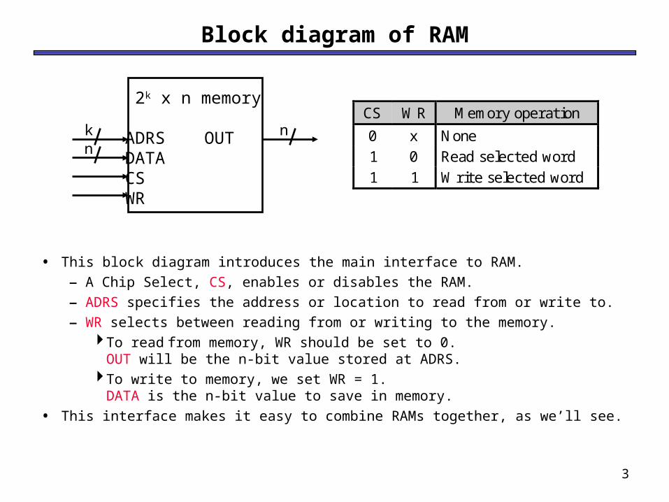
Block diagram of RAM
• This block diagram introduces the main interface to RAM.
– A Chip Select, CS, enables or disables the RAM.
– ADRS specifies the address or location to read from or write to.
– WR selects between reading from or writing to the memory.To read from memory, WR should be set to 0.
OUT will be the n-bit value stored at ADRS.To write to memory, we set WR = 1.
DATA is the n-bit value to save in memory.
• This interface makes it easy to combine RAMs together, as we’ll see.
2k x n memory
ADRS OUTDATACSWR
kn
nCS WR Memory operation
0 x None1 0 Read selected word1 1 Write selected word
4
Memory sizes
• We refer to this as a 2k x n memory.
– There are k address lines, which can specify one of 2k addresses.
– Each address contains an n-bit word.
• For example a 224 x 16 RAM contains 224 = 16M words, each 16 bits long.
– The RAM would need 24 address lines.
– The total storage capacity is 224 x 16 = 228 bits.
2k x n memory
ADRS OUTDATACSWR
kn
n
5
Size matters!
• Memory sizes are usually specified in numbers of bytes (8 bits).
• The 228-bit memory on the previous page translates into:
228 bits / 8 bits per byte = 225 bytes
• With the abbreviations below, this is equivalent to 32 megabytes.
Prefix Base 2 Base 10K Kilo 210 = 1,024 103 = 1,000M Mega 220 = 1,048,576 106 = 1,000,000G Giga 230 = 1,073,741,824 109 = 1,000,000,000
6
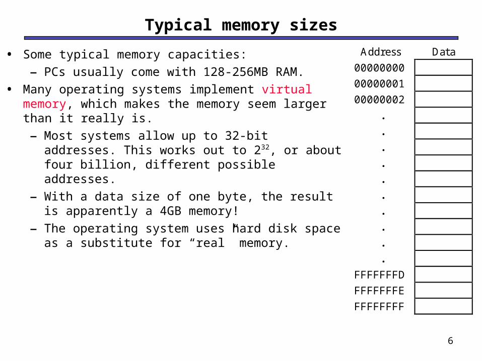
Typical memory sizes
• Some typical memory capacities:
– PCs usually come with 128-256MB RAM.
• Many operating systems implement virtual memory, which makes the memory seem larger than it really is.
– Most systems allow up to 32-bit addresses. This works out to 232, or about four billion, different possible addresses.
– With a data size of one byte, the result is apparently a 4GB memory!
– The operating system uses hard disk space as a substitute for “real” memory.
Address Data
00000000
00000001
00000002
.
.
.
.
.
.
.
.
.
.
FFFFFFFD
FFFFFFFE
FFFFFFFF
7
Reading RAM
• To read from this RAM, the controlling circuit must:
– Enable the chip by ensuring CS = 1.
– Select the read operation, by setting WR = 0.
– Send the desired address to the ADRS input.
– The contents of that address appear on OUT after a little while.
• Notice that the DATA input is unused for read operations.
2k x n memory
ADRS OUTDATACSWR
kn
n
8
Writing RAM
• To write to this RAM, you need to:
– Enable the chip by setting CS = 1.
– Select the write operation, by setting WR = 1.
– Send the desired address to the ADRS input.
– Send the word to store to the DATA input.
• The output OUT is not needed for memory write operations.
2k x n memory
ADRS OUTDATACSWR
kn
n
9
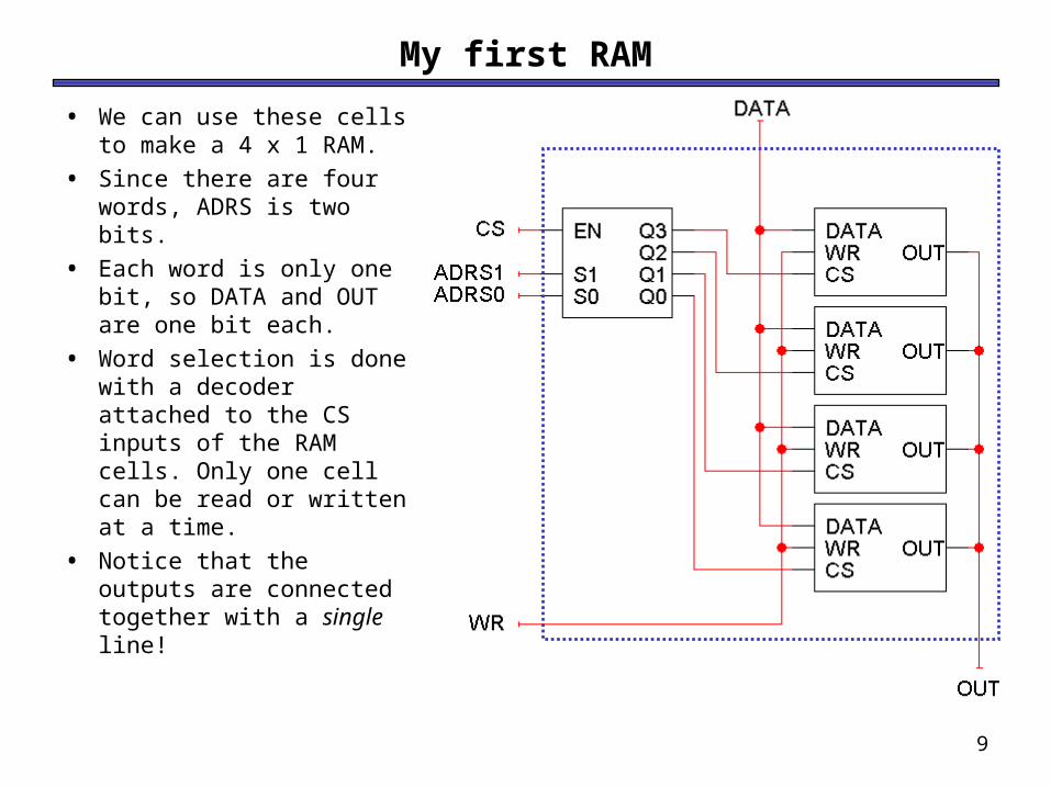
My first RAM
• We can use these cells to make a 4 x 1 RAM.
• Since there are four words, ADRS is two bits.
• Each word is only one bit, so DATA and OUT are one bit each.
• Word selection is done with a decoder attached to the CS inputs of the RAM cells. Only one cell can be read or written at a time.
• Notice that the outputs are connected together with a single line!
10
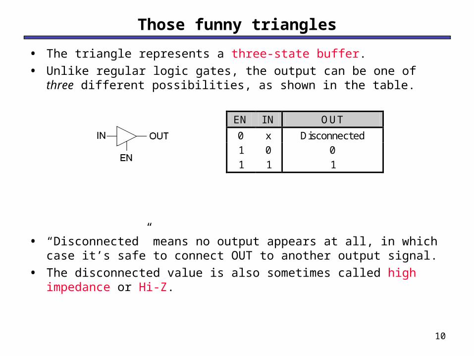
Those funny triangles
• The triangle represents a three-state buffer.
• Unlike regular logic gates, the output can be one of three different possibilities, as shown in the table.
• “Disconnected” means no output appears at all, in which case it’s safe to connect OUT to another output signal.
• The disconnected value is also sometimes called high impedance or Hi-Z.
EN I N OUT
0 x Disconnected 1 0 0 1 1 1
11
Connecting three-state buffers together
• You can connect several three-state buffer outputs together if you can guarantee that only one of them is enabled at any time.
• The easiest way to do this is to use a
decoder!
• If the decoder is disabled, then all the three-state buffers will appear to be disconnected, and OUT will also appear disconnected.
• If the decoder is enabled, then exactly one of its outputs will be true, so only one of the tri-state buffers will be connected and produce an output.
• The net result is we can save some wire and gate costs. We also get a little more flexibility in putting circuits together.
12
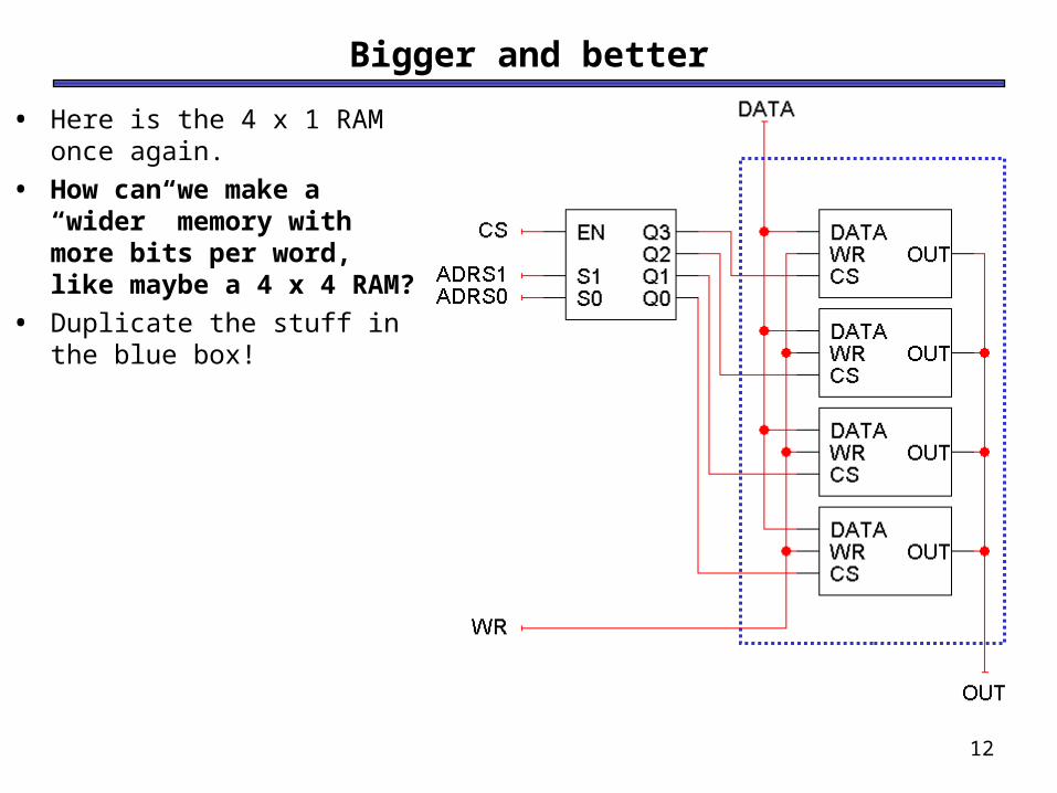
Bigger and better
• Here is the 4 x 1 RAM once again.
• How can we make a “wider” memory with more bits per word, like maybe a 4 x 4 RAM?
• Duplicate the stuff in the blue box!
13
A 4 x 4 RAM
• DATA and OUT are now each four bits long, so you can read and write four-bit words.
14
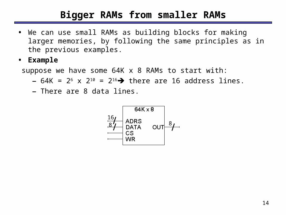
Bigger RAMs from smaller RAMs
• We can use small RAMs as building blocks for making larger memories, by following the same principles as in the previous examples.
• Example suppose we have some 64K x 8 RAMs to start with:
– 64K = 26 x 210 = 216 there are 16 address lines.
– There are 8 data lines.
8816
15
8
8
16
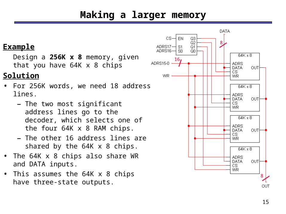
Making a larger memory
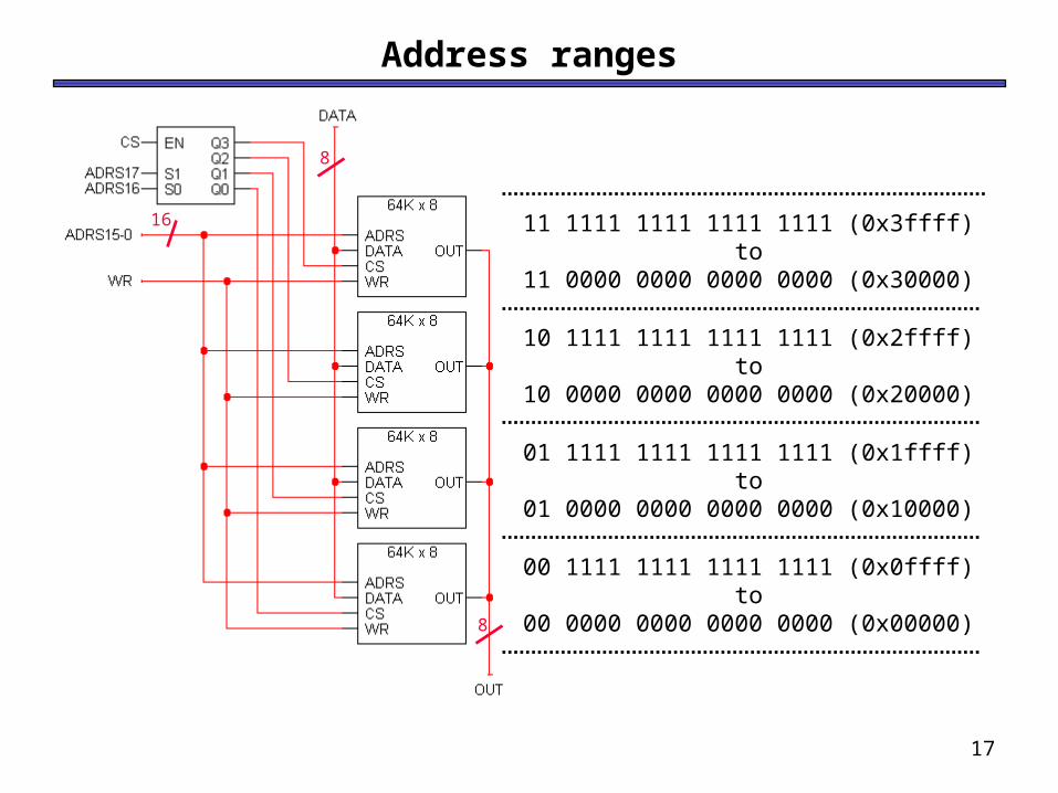
ExampleDesign a 256K x 8 memory, given that you have 64K x 8 chips
Solution• For 256K words, we need 18 address
lines.
– The two most significant address lines go to the decoder, which selects one of the four 64K x 8 RAM chips.
– The other 16 address lines are shared by the 64K x 8 chips.
• The 64K x 8 chips also share WR and DATA inputs.
• This assumes the 64K x 8 chips have three-state outputs.
16
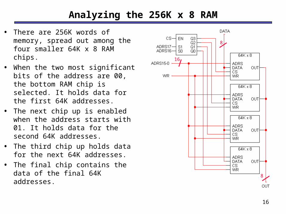
Analyzing the 256K x 8 RAM
• There are 256K words of memory, spread out among the four smaller 64K x 8 RAM chips.
• When the two most significant bits of the address are 00, the bottom RAM chip is selected. It holds data for the first 64K addresses.
• The next chip up is enabled when the address starts with 01. It holds data for the second 64K addresses.
• The third chip up holds data for the next 64K addresses.
• The final chip contains the data of the final 64K addresses.
8
8
16
17
Address ranges
8
8
16 11 1111 1111 1111 1111 (0x3ffff)to
11 0000 0000 0000 0000 (0x30000)
10 1111 1111 1111 1111 (0x2ffff)to
10 0000 0000 0000 0000 (0x20000)
01 1111 1111 1111 1111 (0x1ffff)to
01 0000 0000 0000 0000 (0x10000)
00 1111 1111 1111 1111 (0x0ffff)to
00 0000 0000 0000 0000 (0x00000)
18
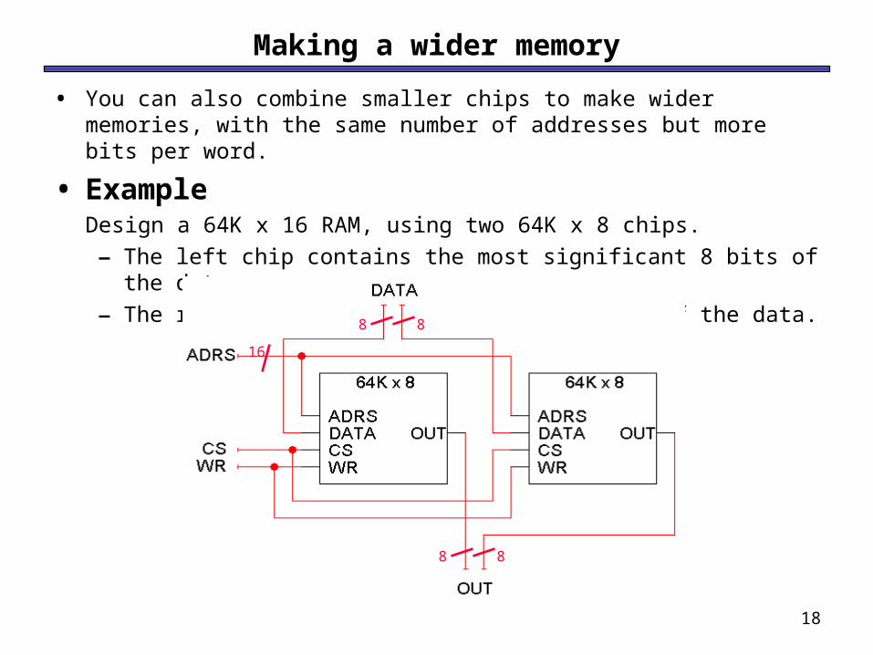
Making a wider memory
• You can also combine smaller chips to make wider memories, with the same number of addresses but more bits per word.
• ExampleDesign a 64K x 16 RAM, using two 64K x 8 chips.
– The left chip contains the most significant 8 bits of the data.
– The right chip contains the lower 8 bits of the data.
16
8 8
8 8
19
Dynamic memory
• Dynamic memory is built with capacitors.
– A stored charge on the capacitor represents a logical 1.
– No charge represents a logic 0.
• However, capacitors lose their charge after a few milliseconds. The memory requires constant refreshing to recharge the capacitors. (That’s what’s “dynamic” about it.)
• Dynamic RAMs tend to be physically smaller than static RAMs.
– A single bit of data can be stored with just one capacitor and one transistor, while static RAM cells typically require 4-6 transistors.
– This means dynamic RAM is cheaper and denser—more bits can be stored in the same physical area.
20
Synchronous DRAM
• Memory chips are organized into “modules” that are connected to the CPU via a 64-bit (8-byte) bus.
• Speeds are rated in megahertz: PC66, PC100 and PC133 memory run at 66MHz, 100MHz and 133MHz respectively.
• Memory bandwidth = # of transfers/sec X size of each transfer
– PC100 can transfer up to 800MB/sec (100MHz x 8 bytes/cycle).
ExampleGiven an SDRAM with bus speed of 100MHz and bus width of 8-bytes, then Find the memory bandwidth?
Memory bandwidth = 100MHz x 8 bytes/cycle
= 800MB/sec
21
Double Data Rate RAM
• Similar to regular SDRAM, except data can be transferred on both the positive and negative clock edges.
• For 100-133MHz buses, the effective memory speeds appear to be 200-266MHz.
• DDR-RAM has lower power consumption, using 2.5V instead of 3.3V like SDRAM. This makes it good for notebooks and other mobile devices.
22
Example
Given a DDR-RAM with bus speed of 100MHz and bus width of 8-bytes. Find the :A)Effective memory speed?
Since data can be transferred on positive and negative edge then
Effective memory speed = 2 X 100MHz
B) Maximum transfer rate? = 200MHz X 8 bytes/cycle
= 1600 MB/s
23
RDRAM
• Another new type of memory called RDRAM is used in the Playstation 2 as well as some Pentium 4 computers.
• The data bus is only 16 bits wide.
• But the memory runs at 400MHz, and data can be transferred on both the positive and negative clock edges.
– That works out to a maximum transfer rate of 1.6GB per second.
– You can also implement two “channels” of memory, resulting in up to 3.2GB/s of bandwidth.
(from amazon.com)
24
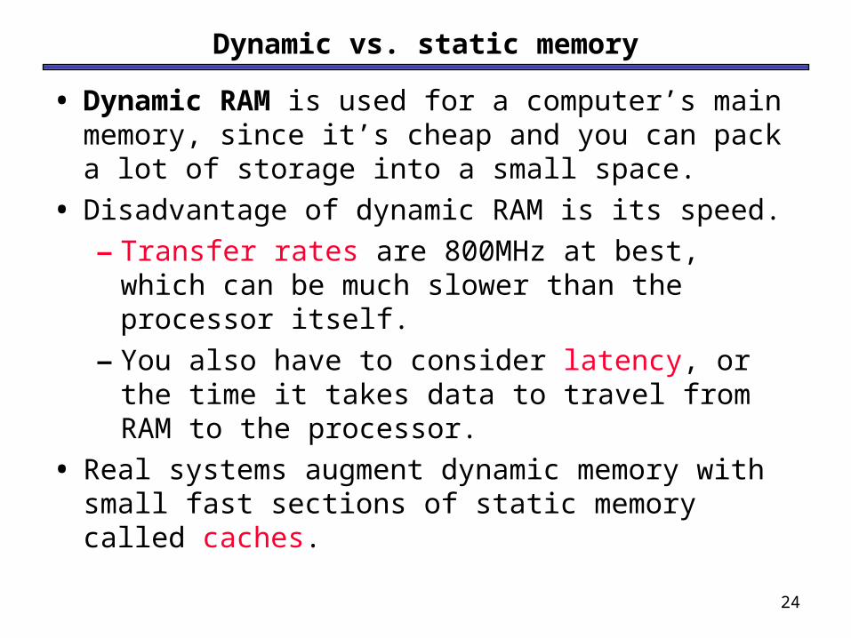
Dynamic vs. static memory
• Dynamic RAM is used for a computer’s main memory, since it’s cheap and you can pack a lot of storage into a small space.
• Disadvantage of dynamic RAM is its speed.
– Transfer rates are 800MHz at best, which can be much slower than the processor itself.
– You also have to consider latency, or the time it takes data to travel from RAM to the processor.
• Real systems augment dynamic memory with small fast sections of static memory called caches.
25
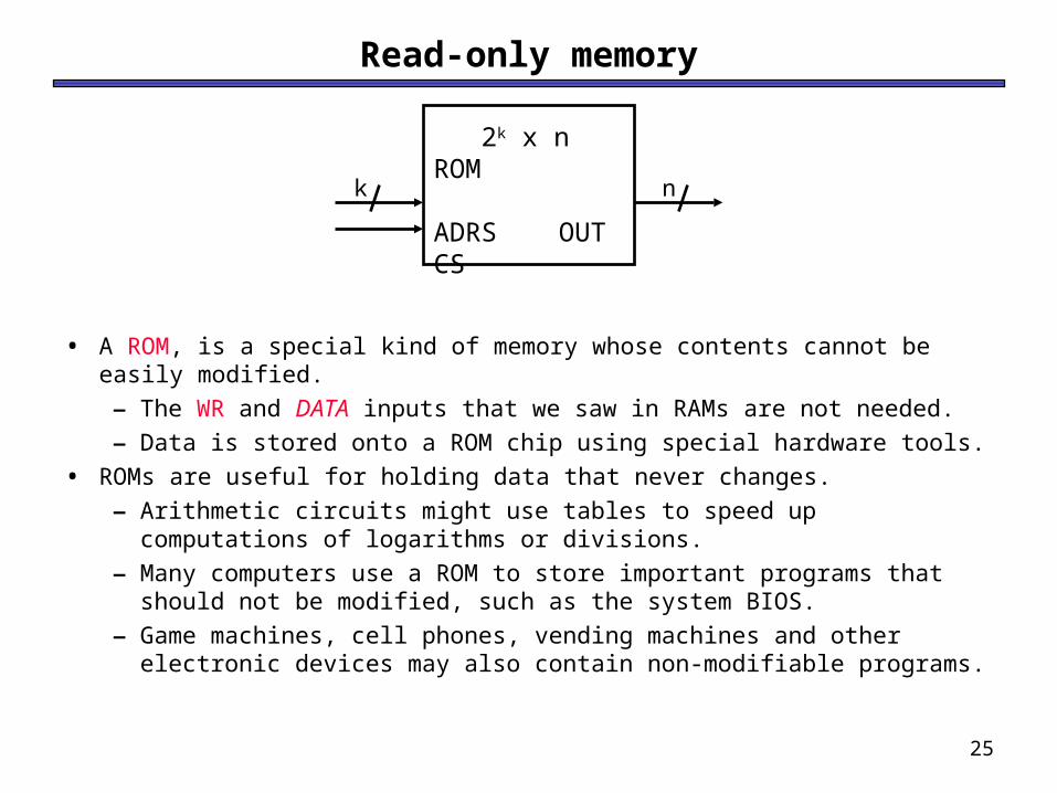
Read-only memory
• A ROM, is a special kind of memory whose contents cannot be easily modified.
– The WR and DATA inputs that we saw in RAMs are not needed.
– Data is stored onto a ROM chip using special hardware tools.
• ROMs are useful for holding data that never changes.
– Arithmetic circuits might use tables to speed up computations of logarithms or divisions.
– Many computers use a ROM to store important programs that should not be modified, such as the system BIOS.
– Game machines, cell phones, vending machines and other electronic devices may also contain non-modifiable programs.
2k x n ROM
ADRS OUTCS
k n
26
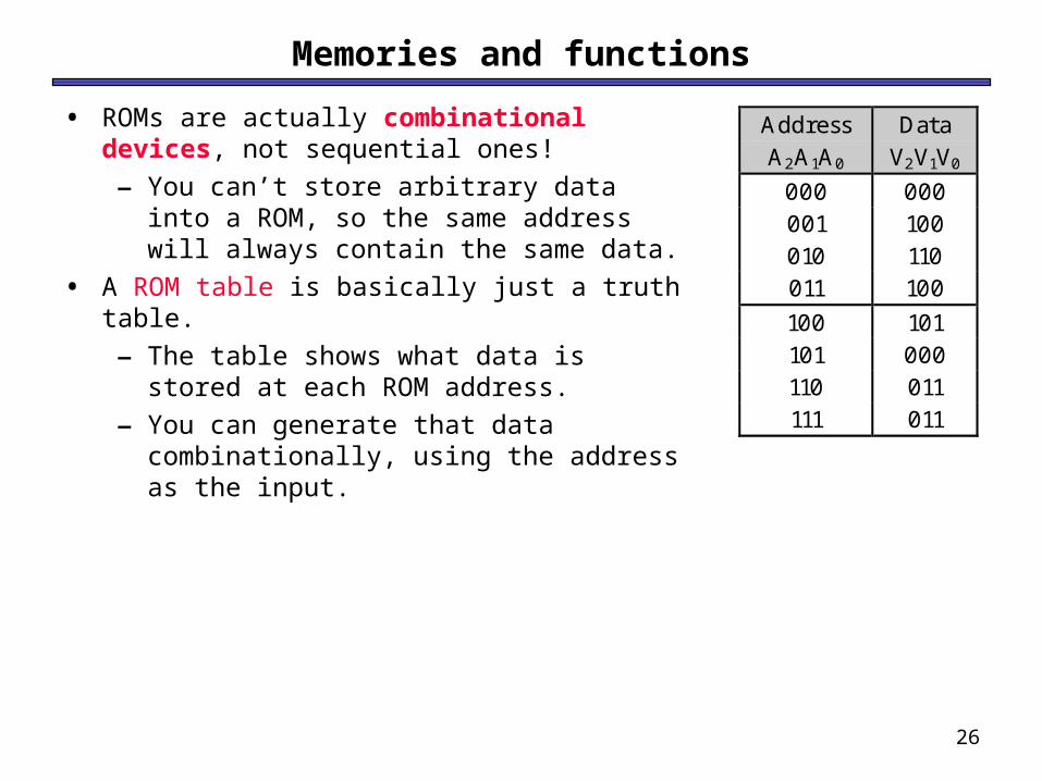
Memories and functions
• ROMs are actually combinational devices, not sequential ones!
– You can’t store arbitrary data into a ROM, so the same address will always contain the same data.
• A ROM table is basically just a truth table.
– The table shows what data is stored at each ROM address.
– You can generate that data combinationally, using the address as the input.
AddressA2A1A0
DataV2V1V0
000 000001 100010 110011 100
100 101101 000110 011111 011
27
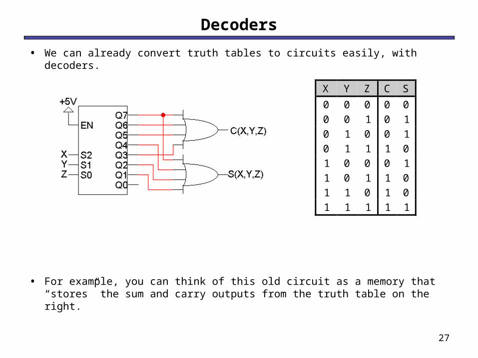
Decoders
• We can already convert truth tables to circuits easily, with decoders.
• For example, you can think of this old circuit as a memory that “stores” the sum and carry outputs from the truth table on the right.
• ROMs are based on this decoder implementation of functions.
– A blank ROM just provides a decoder and several OR gates.
– The connections between the decoder and the OR gates are “programmable,” so different functions can be implemented.
• To program a ROM, you just make the desired connections between the decoder outputs and the OR gate inputs.
29
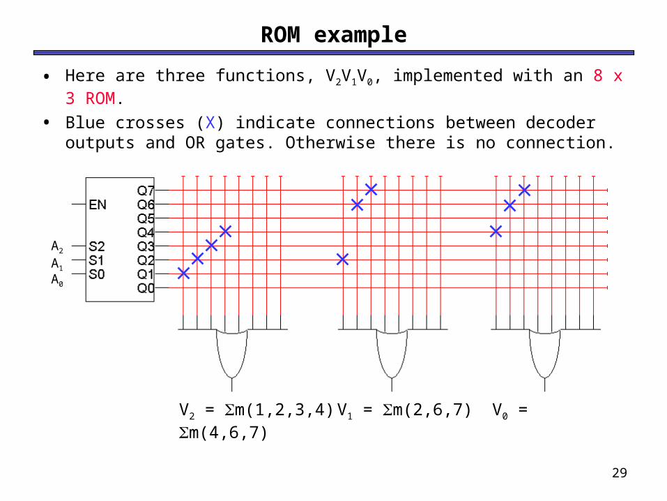
ROM example
• Here are three functions, V2V1V0, implemented with an 8 x 3 ROM.
• Blue crosses (X) indicate connections between decoder outputs and OR gates. Otherwise there is no connection.
V2 = m(1,2,3,4) V1 = m(2,6,7) V0 = m(4,6,7)
A2
A1
A0
30
V2 V1 V0
A2
A1
A0
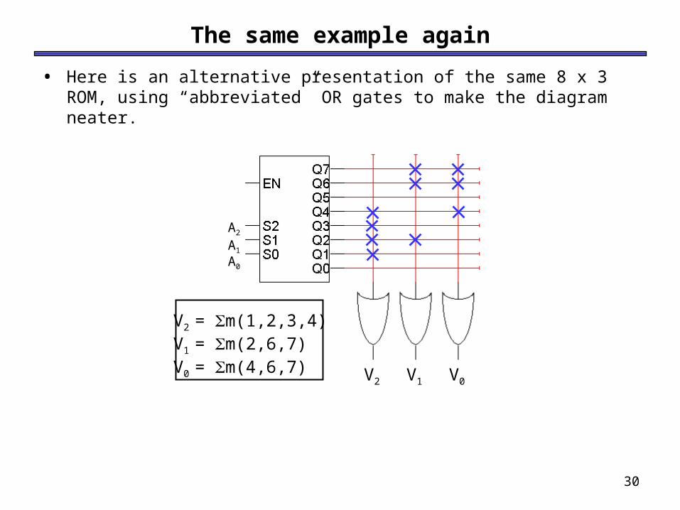
The same example again
• Here is an alternative presentation of the same 8 x 3 ROM, using “abbreviated” OR gates to make the diagram neater.
V2 = m(1,2,3,4)V1 = m(2,6,7)V0 = m(4,6,7)
31
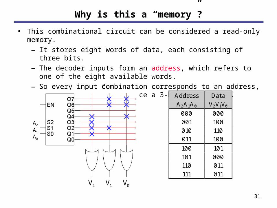
Why is this a “memory”?
• This combinational circuit can be considered a read-only memory.
– It stores eight words of data, each consisting of three bits.
– The decoder inputs form an address, which refers to one of the eight available words.
– So every input combination corresponds to an address, which is “read” to produce a 3-bit data output.
V2 V1 V0
A2
A1
A0
AddressA2A1A0
DataV2V1V0
000 000001 100010 110011 100
100 101101 000110 011111 011
32
Programmable logic arrays
• A ROM is potentially inefficient because it uses a decoder, which generates all possible minterms. No circuit minimization is done.
• Using a ROM to implement an n-input function requires
– An n-to-2n decoder, with n inverters and 2n n-input AND gates.
– An OR gate with up to 2n inputs.
– The number of gates roughly doubles for each additional ROM input.
• A programmable logic array , makes the decoder part of the ROM “programmable” too. Instead of generating all minterms, you can choose which products (not necessarily minterms) to generate.
33
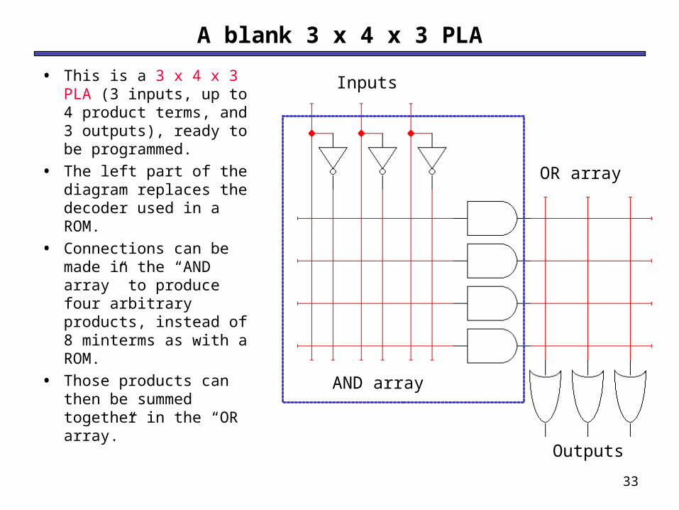
A blank 3 x 4 x 3 PLA
• This is a 3 x 4 x 3 PLA (3 inputs, up to 4 product terms, and 3 outputs), ready to be programmed.
• The left part of the diagram replaces the decoder used in a ROM.
• Connections can be made in the “AND array” to produce four arbitrary products, instead of 8 minterms as with a ROM.
• Those products can then be summed together in the “OR array.”
Inputs
Outputs
AND array
OR array
34
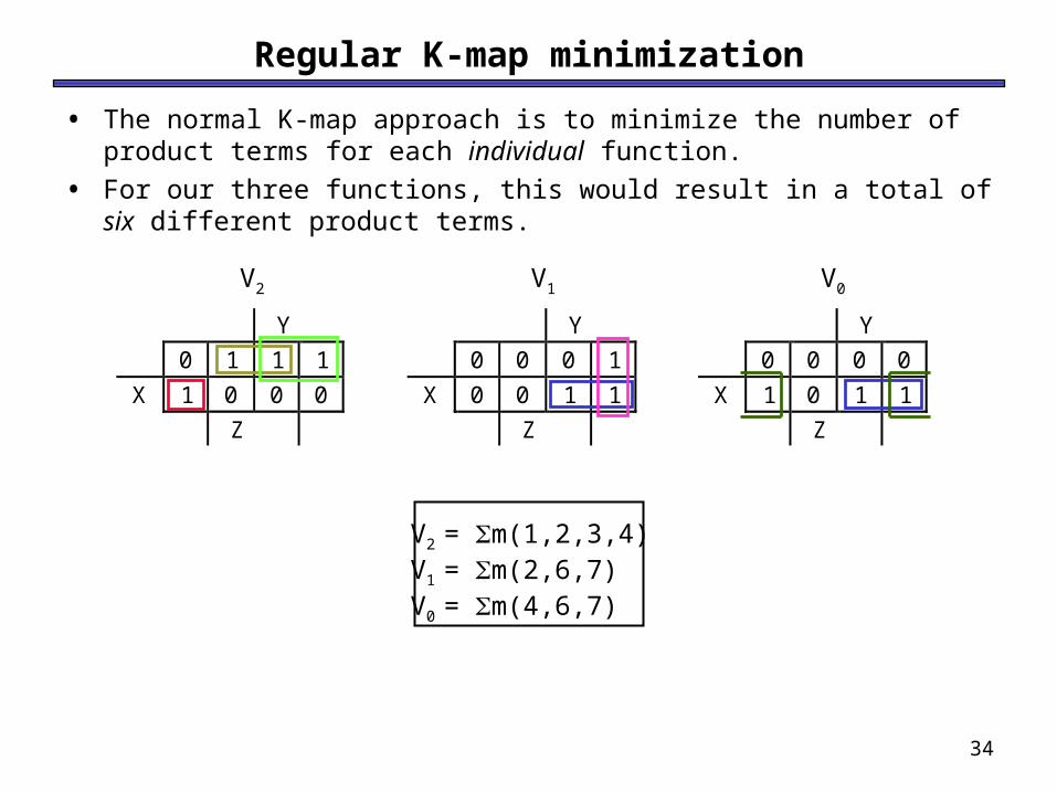
Regular K-map minimization
• The normal K-map approach is to minimize the number of product terms for each individual function.
• For our three functions, this would result in a total of six different product terms.
Y
0 0 0 1
X 0 0 1 1
Z
Y
0 0 0 0
X 1 0 1 1
Z
V2 V1 V0
Y
0 1 1 1
X 1 0 0 0
Z
V2 = m(1,2,3,4)V1 = m(2,6,7)V0 = m(4,6,7)
35
PLA minimization
• For a PLA, we should minimize the number of product terms for all functions together.
• We could express V2, V1 and V0 with just four total products:


![[GUIDE] [PORT] [ROM] All About Mediatek ROM Porting - Xda-Developers](https://static.documents.pub/doc/80x56/55cf9426550346f57b9ff263/guide-port-rom-all-about-mediatek-rom-porting-xda-developers.jpg)

