748
MC9S12DP256/D MC9S12DP256 Advance Information December 1, 2000 Revision 1.1
MC9S12DP256/D
MC9S12DP256
Advance Information
December 1, 2000 Ñ Revision 1.1

MC9S12DP256 — Revision 1.1
MOTOROLA List of Sections 3
List of Sections
List of Sections
List of Sections . . . . . . . . . . . . . . . . . . . . . . . . . . . . . . . . . . 3
Table of Contents . . . . . . . . . . . . . . . . . . . . . . . . . . . . . . . 5
General Description . . . . . . . . . . . . . . . . . . . . . . . . . . . . 13
Central Processing Unit (CPU) . . . . . . . . . . . . . . . . . . . . 19
Pinout and Signal Description . . . . . . . . . . . . . . . . . . . . 41
System Configuration . . . . . . . . . . . . . . . . . . . . . . . . . . . 63
Registers . . . . . . . . . . . . . . . . . . . . . . . . . . . . . . . . . . . . . . 65
Operating Modes . . . . . . . . . . . . . . . . . . . . . . . . . . . . . . 91
Resource Mapping . . . . . . . . . . . . . . . . . . . . . . . . . . . . 107
Bus Control and Input/Output . . . . . . . . . . . . . . . . . . . 123
Resets and Interrupts. . . . . . . . . . . . . . . . . . . . . . . . . . . 141
Voltage Regulator (VREG) . . . . . . . . . . . . . . . . . . . . . . 159
Flash EEPROM 256K . . . . . . . . . . . . . . . . . . . . . . . . . . . . 165
EEPROM 4K . . . . . . . . . . . . . . . . . . . . . . . . . . . . . . . . . . . 193
Port Integration Module . . . . . . . . . . . . . . . . . . . . . . . . 213
List of Sections
MC9S12DP256 — Revision 1.1
4 List of Sections MOTOROLA
Clocks and Reset Generator (CRG). . . . . . . . . . . . . . 257
Pulse Width Modulator (PWM). . . . . . . . . . . . . . . . . . . 297
Enhanced Capture Timer (ECT) . . . . . . . . . . . . . . . . . 341
Serial Communications Interface (SCI) . . . . . . . . . . . 389
Serial Peripheral Interface (SPI) . . . . . . . . . . . . . . . . . 429
Inter-IC Bus (IIC). . . . . . . . . . . . . . . . . . . . . . . . . . . . . . 463
MSCAN . . . . . . . . . . . . . . . . . . . . . . . . . . . . . . . . . . . . . 491
Analog to Digital Converter . . . . . . . . . . . . . . . . . . . . 555
Byte Data Link Controller Module. . . . . . . . . . . . . . . . 603
Background Debug Module (BDM) . . . . . . . . . . . . . . 691
Breakpoint (BKP) Module . . . . . . . . . . . . . . . . . . . . . . 713
Revision History . . . . . . . . . . . . . . . . . . . . . . . . . . . . . . 727
Glossary . . . . . . . . . . . . . . . . . . . . . . . . . . . . . . . . . . . . 729
Literature Updates . . . . . . . . . . . . . . . . . . . . . . . . . . . . 745
MC9S12DP256 — Revision 1.1
MOTOROLA Table of Contents 5
Table of Contents
Table of Contents
List of Sections
Table of Contents
General Description Contents . . . . . . . . . . . . . . . . . . . . . . . . . . . . . . . . . . . . . . . . . . . . . . . 13Introduction . . . . . . . . . . . . . . . . . . . . . . . . . . . . . . . . . . . . . . . . . . . . 13Features . . . . . . . . . . . . . . . . . . . . . . . . . . . . . . . . . . . . . . . . . . . . . . . 14MC9S12DP256 112-Pin Block Diagram . . . . . . . . . . . . . . . . . . . . . . 16Ordering Information . . . . . . . . . . . . . . . . . . . . . . . . . . . . . . . . . . . . . 17
Central Processing Unit (CPU)
Contents . . . . . . . . . . . . . . . . . . . . . . . . . . . . . . . . . . . . . . . . . . . . . . . 19Introduction . . . . . . . . . . . . . . . . . . . . . . . . . . . . . . . . . . . . . . . . . . . . 19Programming Model . . . . . . . . . . . . . . . . . . . . . . . . . . . . . . . . . . . . . . 20Data Types . . . . . . . . . . . . . . . . . . . . . . . . . . . . . . . . . . . . . . . . . . . . . 22Addressing Modes . . . . . . . . . . . . . . . . . . . . . . . . . . . . . . . . . . . . . . . 23Indexed Addressing Modes . . . . . . . . . . . . . . . . . . . . . . . . . . . . . . . . 24Opcodes and Operands . . . . . . . . . . . . . . . . . . . . . . . . . . . . . . . . . . . 25Instruction Set Summary . . . . . . . . . . . . . . . . . . . . . . . . . . . . . . . . . . 26
Pinout and Signal Description
Contents . . . . . . . . . . . . . . . . . . . . . . . . . . . . . . . . . . . . . . . . . . . . . . . 41MC9S12DP256 Pin Assignments in 112-pin QFP . . . . . . . . . . . . . . . 41Power Supply Pins . . . . . . . . . . . . . . . . . . . . . . . . . . . . . . . . . . . . . . . 44Signal Descriptions . . . . . . . . . . . . . . . . . . . . . . . . . . . . . . . . . . . . . . 47Port Signals . . . . . . . . . . . . . . . . . . . . . . . . . . . . . . . . . . . . . . . . . . . . 58
System Configuration
Contents . . . . . . . . . . . . . . . . . . . . . . . . . . . . . . . . . . . . . . . . . . . . . . . 63Introduction . . . . . . . . . . . . . . . . . . . . . . . . . . . . . . . . . . . . . . . . . . . . 63Modules Variabilities . . . . . . . . . . . . . . . . . . . . . . . . . . . . . . . . . . . . . 63MCU Variabilities . . . . . . . . . . . . . . . . . . . . . . . . . . . . . . . . . . . . . . . . 64
Table of Contents
MC9S12DP256 — Revision 1.1
6 Table of Contents MOTOROLA
Registers Contents . . . . . . . . . . . . . . . . . . . . . . . . . . . . . . . . . . . . . . . . . . . . . . 65Register Block . . . . . . . . . . . . . . . . . . . . . . . . . . . . . . . . . . . . . . . . . . 65
Operating Modes Contents . . . . . . . . . . . . . . . . . . . . . . . . . . . . . . . . . . . . . . . . . . . . . . 91Introduction . . . . . . . . . . . . . . . . . . . . . . . . . . . . . . . . . . . . . . . . . . . . 91Operating Modes . . . . . . . . . . . . . . . . . . . . . . . . . . . . . . . . . . . . . . . 91Background Debug Mode . . . . . . . . . . . . . . . . . . . . . . . . . . . . . . . . 102Security . . . . . . . . . . . . . . . . . . . . . . . . . . . . . . . . . . . . . . . . . . . . . . 103
Resource Mapping Contents . . . . . . . . . . . . . . . . . . . . . . . . . . . . . . . . . . . . . . . . . . . . . 107Introduction . . . . . . . . . . . . . . . . . . . . . . . . . . . . . . . . . . . . . . . . . . . 107Internal Resource Mapping . . . . . . . . . . . . . . . . . . . . . . . . . . . . . . . 107Flash EEPROM mapping through internal Memory Expansion . . . 111Miscellaneous System Control Register . . . . . . . . . . . . . . . . . . . . . 118Memory Maps . . . . . . . . . . . . . . . . . . . . . . . . . . . . . . . . . . . . . . . . . 119
Bus Control and Input/Output
Contents . . . . . . . . . . . . . . . . . . . . . . . . . . . . . . . . . . . . . . . . . . . . . 123Introduction . . . . . . . . . . . . . . . . . . . . . . . . . . . . . . . . . . . . . . . . . . . 123Detecting Access Type from External Signals . . . . . . . . . . . . . . . . 123Stretched Bus Cycles . . . . . . . . . . . . . . . . . . . . . . . . . . . . . . . . . . . 124PIPE Status Signals . . . . . . . . . . . . . . . . . . . . . . . . . . . . . . . . . . . . 125Registers . . . . . . . . . . . . . . . . . . . . . . . . . . . . . . . . . . . . . . . . . . . . . 127
Resets and Interrupts
Contents . . . . . . . . . . . . . . . . . . . . . . . . . . . . . . . . . . . . . . . . . . . . . 141Introduction . . . . . . . . . . . . . . . . . . . . . . . . . . . . . . . . . . . . . . . . . . . 141Register Map . . . . . . . . . . . . . . . . . . . . . . . . . . . . . . . . . . . . . . . . . . 142Exception Priority . . . . . . . . . . . . . . . . . . . . . . . . . . . . . . . . . . . . . . 142Maskable interrupts . . . . . . . . . . . . . . . . . . . . . . . . . . . . . . . . . . . . . 143Latching of Interrupts . . . . . . . . . . . . . . . . . . . . . . . . . . . . . . . . . . . 144Register Descriptions . . . . . . . . . . . . . . . . . . . . . . . . . . . . . . . . . . . 147Resets . . . . . . . . . . . . . . . . . . . . . . . . . . . . . . . . . . . . . . . . . . . . . . . 151Effects of Reset . . . . . . . . . . . . . . . . . . . . . . . . . . . . . . . . . . . . . . . . 155Register Stacking . . . . . . . . . . . . . . . . . . . . . . . . . . . . . . . . . . . . . . 157
Voltage Regulator (VREG)
Contents . . . . . . . . . . . . . . . . . . . . . . . . . . . . . . . . . . . . . . . . . . . . . 159Overview . . . . . . . . . . . . . . . . . . . . . . . . . . . . . . . . . . . . . . . . . . . . . 159

Table of Contents
MC9S12DP256 — Revision 1.1
MOTOROLA Table of Contents 7
Features . . . . . . . . . . . . . . . . . . . . . . . . . . . . . . . . . . . . . . . . . . . . . .159Block Diagram . . . . . . . . . . . . . . . . . . . . . . . . . . . . . . . . . . . . . . . . .160Functional Description . . . . . . . . . . . . . . . . . . . . . . . . . . . . . . . . . . .161External Pin Connection . . . . . . . . . . . . . . . . . . . . . . . . . . . . . . . . . .161Reset Initialization . . . . . . . . . . . . . . . . . . . . . . . . . . . . . . . . . . . . . .164Modes of Operation . . . . . . . . . . . . . . . . . . . . . . . . . . . . . . . . . . . . .164
Flash EEPROM 256K
Contents . . . . . . . . . . . . . . . . . . . . . . . . . . . . . . . . . . . . . . . . . . . . . .165Glossary . . . . . . . . . . . . . . . . . . . . . . . . . . . . . . . . . . . . . . . . . . . . . .165Overview . . . . . . . . . . . . . . . . . . . . . . . . . . . . . . . . . . . . . . . . . . . . . .166Features . . . . . . . . . . . . . . . . . . . . . . . . . . . . . . . . . . . . . . . . . . . . . .167Block Diagram . . . . . . . . . . . . . . . . . . . . . . . . . . . . . . . . . . . . . . . . .168Module Memory Map . . . . . . . . . . . . . . . . . . . . . . . . . . . . . . . . . . . .169Functional Description . . . . . . . . . . . . . . . . . . . . . . . . . . . . . . . . . . .174Register Descriptions . . . . . . . . . . . . . . . . . . . . . . . . . . . . . . . . . . . .177External Pin Descriptions . . . . . . . . . . . . . . . . . . . . . . . . . . . . . . . . .190Reset Initialization . . . . . . . . . . . . . . . . . . . . . . . . . . . . . . . . . . . . . .190Modes of Operation . . . . . . . . . . . . . . . . . . . . . . . . . . . . . . . . . . . . .190Low Power Options . . . . . . . . . . . . . . . . . . . . . . . . . . . . . . . . . . . . .190Interrupt Operation . . . . . . . . . . . . . . . . . . . . . . . . . . . . . . . . . . . . . .191
EEPROM 4K Contents . . . . . . . . . . . . . . . . . . . . . . . . . . . . . . . . . . . . . . . . . . . . . .193Glossary . . . . . . . . . . . . . . . . . . . . . . . . . . . . . . . . . . . . . . . . . . . . . .193Overview . . . . . . . . . . . . . . . . . . . . . . . . . . . . . . . . . . . . . . . . . . . . . .194Features . . . . . . . . . . . . . . . . . . . . . . . . . . . . . . . . . . . . . . . . . . . . . .194Block Diagram . . . . . . . . . . . . . . . . . . . . . . . . . . . . . . . . . . . . . . . . .195Module Memory Map . . . . . . . . . . . . . . . . . . . . . . . . . . . . . . . . . . . .195Functional Description . . . . . . . . . . . . . . . . . . . . . . . . . . . . . . . . . . .198Register Descriptions . . . . . . . . . . . . . . . . . . . . . . . . . . . . . . . . . . . .201External Pin Descriptions . . . . . . . . . . . . . . . . . . . . . . . . . . . . . . . . .210Reset Initialization . . . . . . . . . . . . . . . . . . . . . . . . . . . . . . . . . . . . . .210Modes of Operation . . . . . . . . . . . . . . . . . . . . . . . . . . . . . . . . . . . . .210Interrupt Operation . . . . . . . . . . . . . . . . . . . . . . . . . . . . . . . . . . . . . .211
Port Integration Module
Contents . . . . . . . . . . . . . . . . . . . . . . . . . . . . . . . . . . . . . . . . . . . . . .213Overview . . . . . . . . . . . . . . . . . . . . . . . . . . . . . . . . . . . . . . . . . . . . . .213Block Diagram . . . . . . . . . . . . . . . . . . . . . . . . . . . . . . . . . . . . . . . . .215
Table of Contents
MC9S12DP256 — Revision 1.1
8 Table of Contents MOTOROLA
External Pin Descriptions . . . . . . . . . . . . . . . . . . . . . . . . . . . . . . . . 21680 Pin QFP bond-out version . . . . . . . . . . . . . . . . . . . . . . . . . . . . . 216Register Map . . . . . . . . . . . . . . . . . . . . . . . . . . . . . . . . . . . . . . . . . . 217Register Descriptions . . . . . . . . . . . . . . . . . . . . . . . . . . . . . . . . . . . 222Reset Initialization . . . . . . . . . . . . . . . . . . . . . . . . . . . . . . . . . . . . . . 251Functional Description . . . . . . . . . . . . . . . . . . . . . . . . . . . . . . . . . . 251Low Power Options . . . . . . . . . . . . . . . . . . . . . . . . . . . . . . . . . . . . . 255Interrupt Operation . . . . . . . . . . . . . . . . . . . . . . . . . . . . . . . . . . . . . 256
Clocks and Reset Generator (CRG)
Contents . . . . . . . . . . . . . . . . . . . . . . . . . . . . . . . . . . . . . . . . . . . . . 257Overview . . . . . . . . . . . . . . . . . . . . . . . . . . . . . . . . . . . . . . . . . . . . . 257Features . . . . . . . . . . . . . . . . . . . . . . . . . . . . . . . . . . . . . . . . . . . . . 258Block Diagram . . . . . . . . . . . . . . . . . . . . . . . . . . . . . . . . . . . . . . . . . 259Register Map . . . . . . . . . . . . . . . . . . . . . . . . . . . . . . . . . . . . . . . . . . 260Functional Description . . . . . . . . . . . . . . . . . . . . . . . . . . . . . . . . . . 261Register Descriptions . . . . . . . . . . . . . . . . . . . . . . . . . . . . . . . . . . . 279External Pin Descriptions . . . . . . . . . . . . . . . . . . . . . . . . . . . . . . . . 292Reset Initialization . . . . . . . . . . . . . . . . . . . . . . . . . . . . . . . . . . . . . . 294Interrupt Operation . . . . . . . . . . . . . . . . . . . . . . . . . . . . . . . . . . . . . 294Low Power Options . . . . . . . . . . . . . . . . . . . . . . . . . . . . . . . . . . . . . 296
Pulse Width Modulator (PWM)
Contents . . . . . . . . . . . . . . . . . . . . . . . . . . . . . . . . . . . . . . . . . . . . . 297Overview . . . . . . . . . . . . . . . . . . . . . . . . . . . . . . . . . . . . . . . . . . . . . 297Features . . . . . . . . . . . . . . . . . . . . . . . . . . . . . . . . . . . . . . . . . . . . . 298Block Diagram . . . . . . . . . . . . . . . . . . . . . . . . . . . . . . . . . . . . . . . . . 299External Pin Descriptions . . . . . . . . . . . . . . . . . . . . . . . . . . . . . . . . 299Register Map . . . . . . . . . . . . . . . . . . . . . . . . . . . . . . . . . . . . . . . . . . 300Register Descriptions . . . . . . . . . . . . . . . . . . . . . . . . . . . . . . . . . . . 302Functional Description . . . . . . . . . . . . . . . . . . . . . . . . . . . . . . . . . . 324Reset Initialization . . . . . . . . . . . . . . . . . . . . . . . . . . . . . . . . . . . . . . 338Modes of Operation . . . . . . . . . . . . . . . . . . . . . . . . . . . . . . . . . . . . 339Low Power Options . . . . . . . . . . . . . . . . . . . . . . . . . . . . . . . . . . . . . 340Interrupt Operation . . . . . . . . . . . . . . . . . . . . . . . . . . . . . . . . . . . . . 340
Enhanced Capture Timer (ECT)
Contents . . . . . . . . . . . . . . . . . . . . . . . . . . . . . . . . . . . . . . . . . . . . . 341Overview . . . . . . . . . . . . . . . . . . . . . . . . . . . . . . . . . . . . . . . . . . . . . 341Features . . . . . . . . . . . . . . . . . . . . . . . . . . . . . . . . . . . . . . . . . . . . . 342
Table of Contents
MC9S12DP256 — Revision 1.1
MOTOROLA Table of Contents 9
Modes of Operation . . . . . . . . . . . . . . . . . . . . . . . . . . . . . . . . . . . . .342Abbreviations . . . . . . . . . . . . . . . . . . . . . . . . . . . . . . . . . . . . . . . . . .342Block Diagram . . . . . . . . . . . . . . . . . . . . . . . . . . . . . . . . . . . . . . . . .344Signal Descriptions . . . . . . . . . . . . . . . . . . . . . . . . . . . . . . . . . . . . . .350Module Memory Map . . . . . . . . . . . . . . . . . . . . . . . . . . . . . . . . . . . .351Register Quick Reference . . . . . . . . . . . . . . . . . . . . . . . . . . . . . . . .354Register Descriptions . . . . . . . . . . . . . . . . . . . . . . . . . . . . . . . . . . . .356Modes of Operation . . . . . . . . . . . . . . . . . . . . . . . . . . . . . . . . . . . . .383Interrupts . . . . . . . . . . . . . . . . . . . . . . . . . . . . . . . . . . . . . . . . . . . . .386Description of Interrupt Operation . . . . . . . . . . . . . . . . . . . . . . . . . .387
Serial Communications Interface (SCI)
Contents . . . . . . . . . . . . . . . . . . . . . . . . . . . . . . . . . . . . . . . . . . . . . .389Overview . . . . . . . . . . . . . . . . . . . . . . . . . . . . . . . . . . . . . . . . . . . . . .389Features . . . . . . . . . . . . . . . . . . . . . . . . . . . . . . . . . . . . . . . . . . . . . .389Modes of Operation . . . . . . . . . . . . . . . . . . . . . . . . . . . . . . . . . . . . .390SCI Interface Diagram . . . . . . . . . . . . . . . . . . . . . . . . . . . . . . . . . . .392Block Diagram . . . . . . . . . . . . . . . . . . . . . . . . . . . . . . . . . . . . . . . . .392Signal Descriptions . . . . . . . . . . . . . . . . . . . . . . . . . . . . . . . . . . . . . .393Module Memory Map . . . . . . . . . . . . . . . . . . . . . . . . . . . . . . . . . . . .394Register Quick Reference . . . . . . . . . . . . . . . . . . . . . . . . . . . . . . . .395Register Descriptions . . . . . . . . . . . . . . . . . . . . . . . . . . . . . . . . . . . .396Functional Description . . . . . . . . . . . . . . . . . . . . . . . . . . . . . . . . . . .406Modes of Operation . . . . . . . . . . . . . . . . . . . . . . . . . . . . . . . . . . . . .424Interrupt Operation . . . . . . . . . . . . . . . . . . . . . . . . . . . . . . . . . . . . . .425
Serial Peripheral Interface (SPI)
Contents . . . . . . . . . . . . . . . . . . . . . . . . . . . . . . . . . . . . . . . . . . . . . .429Overview . . . . . . . . . . . . . . . . . . . . . . . . . . . . . . . . . . . . . . . . . . . . . .429Features . . . . . . . . . . . . . . . . . . . . . . . . . . . . . . . . . . . . . . . . . . . . . .430Modes of Operation . . . . . . . . . . . . . . . . . . . . . . . . . . . . . . . . . . . . .430Block Diagram . . . . . . . . . . . . . . . . . . . . . . . . . . . . . . . . . . . . . . . . .431Signal Descriptions . . . . . . . . . . . . . . . . . . . . . . . . . . . . . . . . . . . . . .432Module Memory Map . . . . . . . . . . . . . . . . . . . . . . . . . . . . . . . . . . . .436Register Quick Reference . . . . . . . . . . . . . . . . . . . . . . . . . . . . . . . .437Register Descriptions . . . . . . . . . . . . . . . . . . . . . . . . . . . . . . . . . . . .438Functional Description . . . . . . . . . . . . . . . . . . . . . . . . . . . . . . . . . . .446Low Power Mode Options . . . . . . . . . . . . . . . . . . . . . . . . . . . . . . . .457Errata . . . . . . . . . . . . . . . . . . . . . . . . . . . . . . . . . . . . . . . . . . . . . . . .459
Table of Contents
MC9S12DP256 — Revision 1.1
10 Table of Contents MOTOROLA
Reset . . . . . . . . . . . . . . . . . . . . . . . . . . . . . . . . . . . . . . . . . . . . . . . . 460Interrupts . . . . . . . . . . . . . . . . . . . . . . . . . . . . . . . . . . . . . . . . . . . . . 460
Inter-IC Bus (IIC) Contents . . . . . . . . . . . . . . . . . . . . . . . . . . . . . . . . . . . . . . . . . . . . . 463Overview . . . . . . . . . . . . . . . . . . . . . . . . . . . . . . . . . . . . . . . . . . . . . 463Features . . . . . . . . . . . . . . . . . . . . . . . . . . . . . . . . . . . . . . . . . . . . . 464Modes of Operation . . . . . . . . . . . . . . . . . . . . . . . . . . . . . . . . . . . . 464Block Diagram . . . . . . . . . . . . . . . . . . . . . . . . . . . . . . . . . . . . . . . . . 465Signal Descriptions . . . . . . . . . . . . . . . . . . . . . . . . . . . . . . . . . . . . . 467Module Memory Map . . . . . . . . . . . . . . . . . . . . . . . . . . . . . . . . . . . 468Register Quick Reference . . . . . . . . . . . . . . . . . . . . . . . . . . . . . . . . 469Register Descriptions . . . . . . . . . . . . . . . . . . . . . . . . . . . . . . . . . . . 469I-Bus Protocol . . . . . . . . . . . . . . . . . . . . . . . . . . . . . . . . . . . . . . . . . 478Interrupt Operation . . . . . . . . . . . . . . . . . . . . . . . . . . . . . . . . . . . . . 483Modes of Operation . . . . . . . . . . . . . . . . . . . . . . . . . . . . . . . . . . . . 484Programming . . . . . . . . . . . . . . . . . . . . . . . . . . . . . . . . . . . . . . . . . 485
MSCAN Contents . . . . . . . . . . . . . . . . . . . . . . . . . . . . . . . . . . . . . . . . . . . . . 491Overview . . . . . . . . . . . . . . . . . . . . . . . . . . . . . . . . . . . . . . . . . . . . . 491Features . . . . . . . . . . . . . . . . . . . . . . . . . . . . . . . . . . . . . . . . . . . . . 492Block Diagram . . . . . . . . . . . . . . . . . . . . . . . . . . . . . . . . . . . . . . . . . 493External Pin Descriptions . . . . . . . . . . . . . . . . . . . . . . . . . . . . . . . . 494Register Map . . . . . . . . . . . . . . . . . . . . . . . . . . . . . . . . . . . . . . . . . . 496Functional Description . . . . . . . . . . . . . . . . . . . . . . . . . . . . . . . . . . 499Register Descriptions . . . . . . . . . . . . . . . . . . . . . . . . . . . . . . . . . . . 512Modes of Operation . . . . . . . . . . . . . . . . . . . . . . . . . . . . . . . . . . . . 546Low Power Options . . . . . . . . . . . . . . . . . . . . . . . . . . . . . . . . . . . . . 547Interrupt Operation . . . . . . . . . . . . . . . . . . . . . . . . . . . . . . . . . . . . . 553
Analog to Digital Converter
Contents . . . . . . . . . . . . . . . . . . . . . . . . . . . . . . . . . . . . . . . . . . . . . 555Overview . . . . . . . . . . . . . . . . . . . . . . . . . . . . . . . . . . . . . . . . . . . . . 555Features . . . . . . . . . . . . . . . . . . . . . . . . . . . . . . . . . . . . . . . . . . . . . 556Block Diagram . . . . . . . . . . . . . . . . . . . . . . . . . . . . . . . . . . . . . . . . . 557Register Map . . . . . . . . . . . . . . . . . . . . . . . . . . . . . . . . . . . . . . . . . . 559Functional Description . . . . . . . . . . . . . . . . . . . . . . . . . . . . . . . . . . 561Register Descriptions . . . . . . . . . . . . . . . . . . . . . . . . . . . . . . . . . . . 572External Pin Descriptions . . . . . . . . . . . . . . . . . . . . . . . . . . . . . . . . 595

Table of Contents
MC9S12DP256 — Revision 1.1
MOTOROLA Table of Contents 11
Reset Initialization . . . . . . . . . . . . . . . . . . . . . . . . . . . . . . . . . . . . . .596Modes of Operation . . . . . . . . . . . . . . . . . . . . . . . . . . . . . . . . . . . . .597Sample Conversion . . . . . . . . . . . . . . . . . . . . . . . . . . . . . . . . . . . . .599General Purpose Input Ports . . . . . . . . . . . . . . . . . . . . . . . . . . . . . .602
Byte Data Link Controller Module
Contents . . . . . . . . . . . . . . . . . . . . . . . . . . . . . . . . . . . . . . . . . . . . . .603Overview . . . . . . . . . . . . . . . . . . . . . . . . . . . . . . . . . . . . . . . . . . . . . .603Features . . . . . . . . . . . . . . . . . . . . . . . . . . . . . . . . . . . . . . . . . . . . . .604Block Diagram . . . . . . . . . . . . . . . . . . . . . . . . . . . . . . . . . . . . . . . . .605Register Map . . . . . . . . . . . . . . . . . . . . . . . . . . . . . . . . . . . . . . . . . .606Functional Description . . . . . . . . . . . . . . . . . . . . . . . . . . . . . . . . . . .607Register Descriptions . . . . . . . . . . . . . . . . . . . . . . . . . . . . . . . . . . . .633External Pin Descriptions . . . . . . . . . . . . . . . . . . . . . . . . . . . . . . . . .653Reset Initialization/Basic Operation . . . . . . . . . . . . . . . . . . . . . . . . .653Transmitting A Message . . . . . . . . . . . . . . . . . . . . . . . . . . . . . . . . .658Receiving A Message . . . . . . . . . . . . . . . . . . . . . . . . . . . . . . . . . . .664Transmitting An In-Frame Response (IFR) . . . . . . . . . . . . . . . . . . .669Receiving An In-Frame Response (IFR) . . . . . . . . . . . . . . . . . . . . .681Special BDLC Operations . . . . . . . . . . . . . . . . . . . . . . . . . . . . . . . .683Modes of Operation . . . . . . . . . . . . . . . . . . . . . . . . . . . . . . . . . . . . .684Interrupt Operation . . . . . . . . . . . . . . . . . . . . . . . . . . . . . . . . . . . . . .689Low Power Options . . . . . . . . . . . . . . . . . . . . . . . . . . . . . . . . . . . . .689
Background Debug Module (BDM)
Contents . . . . . . . . . . . . . . . . . . . . . . . . . . . . . . . . . . . . . . . . . . . . . .691Overview . . . . . . . . . . . . . . . . . . . . . . . . . . . . . . . . . . . . . . . . . . . . . .691Interface Signals . . . . . . . . . . . . . . . . . . . . . . . . . . . . . . . . . . . . . . . .692Registers . . . . . . . . . . . . . . . . . . . . . . . . . . . . . . . . . . . . . . . . . . . . .693Operation . . . . . . . . . . . . . . . . . . . . . . . . . . . . . . . . . . . . . . . . . . . . .698Modes of Operation . . . . . . . . . . . . . . . . . . . . . . . . . . . . . . . . . . . . .710Low-Power Options . . . . . . . . . . . . . . . . . . . . . . . . . . . . . . . . . . . . .711Interrupt Operation . . . . . . . . . . . . . . . . . . . . . . . . . . . . . . . . . . . . . .711
Breakpoint (BKP) Module
Contents . . . . . . . . . . . . . . . . . . . . . . . . . . . . . . . . . . . . . . . . . . . . . .713Overview . . . . . . . . . . . . . . . . . . . . . . . . . . . . . . . . . . . . . . . . . . . . . .713Features . . . . . . . . . . . . . . . . . . . . . . . . . . . . . . . . . . . . . . . . . . . . . .714Block Diagram . . . . . . . . . . . . . . . . . . . . . . . . . . . . . . . . . . . . . . . . .715External Pin Descriptions . . . . . . . . . . . . . . . . . . . . . . . . . . . . . . . . .716
Table of Contents
MC9S12DP256 — Revision 1.1
12 Table of Contents MOTOROLA
Register Descriptions . . . . . . . . . . . . . . . . . . . . . . . . . . . . . . . . . . . 716Functional Description . . . . . . . . . . . . . . . . . . . . . . . . . . . . . . . . . . 723Breakpoint Operating Modes . . . . . . . . . . . . . . . . . . . . . . . . . . . . . 724Breakpoint Types . . . . . . . . . . . . . . . . . . . . . . . . . . . . . . . . . . . . . . 725Modes of Operation . . . . . . . . . . . . . . . . . . . . . . . . . . . . . . . . . . . . 725Low Power Options . . . . . . . . . . . . . . . . . . . . . . . . . . . . . . . . . . . . . 726Reset Initialization . . . . . . . . . . . . . . . . . . . . . . . . . . . . . . . . . . . . . . 726Interrupt Operation . . . . . . . . . . . . . . . . . . . . . . . . . . . . . . . . . . . . . 726General Purpose I/O Ports . . . . . . . . . . . . . . . . . . . . . . . . . . . . . . . 726
Revision History Changes from Rev 1.0 to Rev 1.1 . . . . . . . . . . . . . . . . . . . . . . . . . . 727
Glossary
Literature Updates Literature Distribution Centers . . . . . . . . . . . . . . . . . . . . . . . . . . . . 745Customer Focus Center . . . . . . . . . . . . . . . . . . . . . . . . . . . . . . . . . 746Microcontroller Division’s Web Site . . . . . . . . . . . . . . . . . . . . . . . . . 746
MC9S12DP256 — Revision 1.1
MOTOROLA General Description 13
General Description
General Description
Contents
Introduction . . . . . . . . . . . . . . . . . . . . . . . . . . . . . . . . . . . . . . . . . . . . . 13Features . . . . . . . . . . . . . . . . . . . . . . . . . . . . . . . . . . . . . . . . . . . . . . . 14MC9S12DP256 112-Pin Block Diagram . . . . . . . . . . . . . . . . . . . . . . . 16Ordering Information . . . . . . . . . . . . . . . . . . . . . . . . . . . . . . . . . . . . . . 17
Introduction
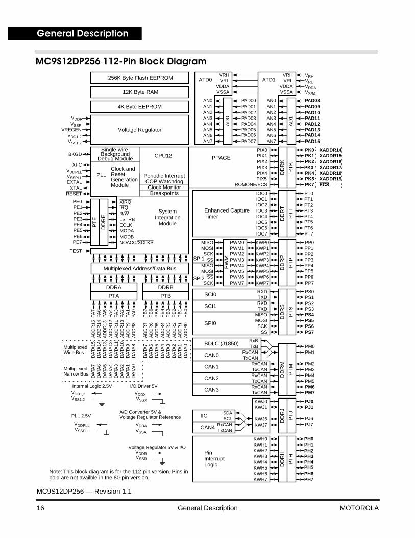
The MC9S12DP256 microcontroller unit (MCU) is a 16-bit device composed of standard on-chip peripherals including a 16-bit central processing unit (STAR12 CPU), 256K bytes of Flash EEPROM, 12.0K bytes of RAM, 4.0K bytes of EEPROM, 2 asynchronous serial communications interfaces (SCI), three serial peripheral interfaces (SPI), an 8 channel IC/OC enhanced capture timer, two 8-channel, 10-bit analog-to-digital converters (ADC), an 8-channel pulse-width modulator (PWM), a digital Byte Data Link Controller (BDLC), 29 discrete digital I/O channels (Port A, Port B, Port K and Port E), 20 discrete digital I/O lines with interrupt and wakeup capability, five CAN 2.0 A, B software compatible modules (MSCAN12), and an Inter-IC Bus. System resource mapping, clock generation, interrupt control and bus interfacing are managed by the System Integration Module (SIM). The MC9S12DP256 has full 16-bit data paths throughout. However, the external bus can operate in an 8-bit narrow mode so single 8-bit wide memory can be interfaced for lower cost systems. The inclusion of a PLL circuit allows power consumption and performance to be adjusted to suit operational requirements.
NOTE:
The main body of this document refers to the 112-pin version of the device. Pins shown in bold on the block diagram and pinout are not available on the 80-pin version.
General Description
MC9S12DP256 — Revision 1.1
14 General Description MOTOROLA
Features
• 16-bit STAR12 CPU
– Upward compatible with M68HC11 instruction set
– Interrupt stacking and programmer’s model identical to M68HC11
– 20-bit ALU
– Instruction pipe
– Enhanced indexed addressing
• Multiplexed External Bus
• Memory
– 256K byte Flash EEPROM
– 4.0K byte EEPROM
– 12.0K byte RAM
• Two 8 channel Analog-to-Digital Converters
– 10-bit resolution
• Five 1M bit per second, CAN 2.0 A, B software compatible modules
– Four receive and three transmit buffers
– Flexible identifier filter programmable as 2 x 32 bit, 4 x 16 bit or 8 x 8 bit
– Four separate interrupt channels for Rx, Tx, error and wake-up
– Low-pass filter wake-up function
– Loop-back for self test operation
– Time-stamping capabilities for network synchronization
• 8 channel IC/OC Enhanced Capture Timer
• Byte Data Link Controller (BDLC)
• Inter-IC Bus (IIC)

General DescriptionFeatures
MC9S12DP256 — Revision 1.1
MOTOROLA General Description 15
• 8 PWM channels with programmable period and duty cycle
– Standard 8-bit 8-channel or 16-bit 4-channel or any combination of 8/16 bit
– Separate control for each pulse width and duty cycle
– Left-aligned or center-aligned outputs
– Programmable clock select logic with a wide range of frequencies
– Fast emergency shutdown input
– Usable as interrupt inputs
• Serial interfaces
– Two asynchronous Serial Communications Interfaces (SCI)
– Three synchronous Serial Peripheral Interfaces (SPI)
• SIM (System integration module)
– CRG (low current oscillator, PLL, reset, clocks, COP watchdog, real time interrupt, clock monitor)
– MEBI (Multiplexed External Bus Interface)
– MMC (Module Mapping Control)
– INT (Interrupt control)
– BKP (Breakpoints)
– BDM (Background Debug Mode)
• 112-Pin LQFP package or 80-Pin QFP package
– 50 MHz CPU equivalent to 25MHz bus operation
– 2.25 to 2.75V Digital Supply Voltage generated using an internal voltage regulator
– 4.75V to 5.25V Analog and I/O Supply Voltage
• Technology: 0.25 micron CMOS
General Description
MC9S12DP256 — Revision 1.1
16 General Description MOTOROLA
MC9S12DP256 112-Pin Block Diagram
256K Byte Flash EEPROM
12K Byte RAM
Enhanced Capture
RESET
EXTALXTAL
VDD1,2VSS1,2
SCI0
4K Byte EEPROM
BKGD
R/W
MODB
XIRQ
NOACC/XCLKS
SystemIntegration
Module
VDDR
CPU12
Periodic InterruptCOP WatchdogClock Monitor
Single-wire
Breakpoints
PLLVSSPLL
XFCVDDPLL
Multiplexed Address/Data Bus
VDDAVSSA
VRHVRLATD0
MultiplexedWide Bus
Multiplexed
VDDX VSSX
Internal Logic 2.5V
Narrow Bus
PPAGE
VDDPLL VSSPLL
PLL 2.5V
IRQ
LSTRBECLKMODA
PA4
PA3
PA2
PA1
PA0
PA7
PA6
PA5
TEST
AD
DR
12A
DD
R11
AD
DR
10A
DD
R9
AD
DR
8
AD
DR
15A
DD
R14
AD
DR
13D
ATA
12D
ATA
11D
ATA
10D
ATA
9D
ATA
8
DAT
A15
DAT
A14
DAT
A13
PB
4P
B3
PB
2P
B1
PB
0
PB
7P
B6
PB
5A
DD
R4
AD
DR
3A
DD
R2
AD
DR
1A
DD
R0
AD
DR
7A
DD
R6
AD
DR
5D
ATA
4D
ATA
3D
ATA
2D
ATA
1D
ATA
0
DAT
A7
DAT
A6
DAT
A5
DAT
A4
DAT
A3
DAT
A2
DAT
A1
DAT
A0
DAT
A7
DAT
A6
DAT
A5
PE3PE4PE5PE6PE7
PE0PE1PE2
AN2
AN6
AN0
AN7
AN1
AN3AN4AN5
PAD03PAD04PAD05PAD06PAD07
PAD00PAD01PAD02
IOC2
IOC6
IOC0
IOC7
IOC1
IOC3IOC4IOC5
PT3PT4PT5PT6PT7
PT0PT1PT2
VRHVRL
VDDAVSSA
VRHVRLATD1
AN2
AN6
AN0
AN7
AN1
AN3AN4AN5
PAD11PAD12PAD13PAD14PAD15
PAD08PAD09PAD10
VDDAVSSA
RXDTXD
MISOMOSI
PS3PS4PS5
PS0PS1PS2SCI1 RXD
TXD
PW
M
PWM2
PWM6
PWM0
PWM7
PWM1
PWM3PWM4PWM5
PP3PP4PP5PP6PP7
PP0PP1PP2
PIX2
PIX0PIX1
PIX3
ROMONE/ECS
PK3
PK7
PK0PK1
XADDR17
ECS
XADDR14XADDR15XADDR16
SCKSS
PS6PS7
SPI0
IIC SDASCL PJ6
PJ7
CAN0 RxCANTxCAN
PM1PM0
CAN1 RxCANTxCAN
PM2PM3
CAN2 RxCANTxCAN
PM4PM5
CAN3 RxCANTxCAN
PM6PM7
Pin KWH2
KWH6
KWH0
KWH7
KWH1
KWH3KWH4KWH5
PH3PH4PH5PH6PH7
PH0PH1PH2
KWJ0KWJ1
PJ0PJ1
I/O Driver 5V
VDDAVSSA
A/D Converter 5V &
DDRA DDRB
PTA PTB
DD
RE
PT
E
AD
1
AD
0
PT
K
DD
RK
PT
T
DD
RT
PT
P
DD
RP
PT
S
DD
RS
PT
M
DD
RM
PT
H
DD
RH
PT
J
DD
RJ
PK2
BDLC (J1850) RxBTxB
InterruptLogic
Clock andResetGenerationModule
Voltage RegulatorVSSR
Background
VDD1,2VSS1,2
VREGEN
VDDRVSSR
Voltage Regulator 5V & I/O
CAN4 RxCANTxCAN
MISOMOSI
SSSCK
SPI2
MISOMOSISCK
SSSPI1
PIX4PIX5
PK4PK5
XADDR18XADDR19
Voltage Regulator Reference
KWP2
KWP6
KWP0
KWP7
KWP1
KWP3KWP4KWP5
KWJ6KWJ7
Timer
Debug Module
Note: This block diagram is for the 112-pin version. Pins in bold are not availble in the 80-pin version.
General DescriptionOrdering Information
MC9S12DP256 — Revision 1.1
MOTOROLA General Description 17
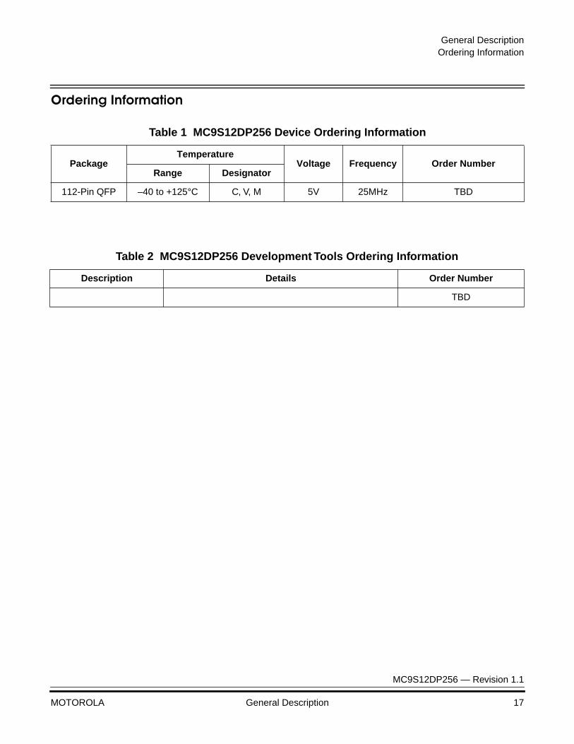
Ordering Information
Table 1 MC9S12DP256 Device Ordering Information
PackageTemperature
Voltage Frequency Order NumberRange Designator
112-Pin QFP –40 to +125
°
C C, V, M 5V 25MHz TBD
Table 2 MC9S12DP256 Development Tools Ordering Information
Description Details Order Number
TBD

General Description
MC9S12DP256 — Revision 1.1
18 General Description MOTOROLA
MC9S12DP256 — Revision 1.1
MOTOROLA Central Processing Unit (CPU) 19
Central Processing Unit (CPU)
Central Processing Unit (CPU)
Contents
Introduction . . . . . . . . . . . . . . . . . . . . . . . . . . . . . . . . . . . . . . . . . . . . . 19Programming Model . . . . . . . . . . . . . . . . . . . . . . . . . . . . . . . . . . . . . . 20Data Types . . . . . . . . . . . . . . . . . . . . . . . . . . . . . . . . . . . . . . . . . . . . . 22Addressing Modes . . . . . . . . . . . . . . . . . . . . . . . . . . . . . . . . . . . . . . . 23Indexed Addressing Modes. . . . . . . . . . . . . . . . . . . . . . . . . . . . . . . . . 24Opcodes and Operands . . . . . . . . . . . . . . . . . . . . . . . . . . . . . . . . . . . 25Set Instruction Summary. . . . . . . . . . . . . . . . . . . . . . . . . . . . . . . . . . . 24
Introduction
The STAR12 CPU is a high-speed, 16-bit processing unit. It has full 16-bit data paths and wider internal registers (up to 20 bits) for high-speed extended math instructions. The instruction set is a proper superset of the M68HC11instruction set. The STAR12 CPU allows instructions with odd byte counts, including many single-byte instructions. This provides efficient use of ROM space. An instruction pipe buffers program information so the CPU always has immediate access to at least three bytes of machine code at the start of every instruction. The STAR12 CPU also offers an extensive set of indexed addressing capabilities.
Central Processing Unit (CPU)
MC9S12DP256 — Revision 1.1
20 Central Processing Unit (CPU) MOTOROLA
Programming Model
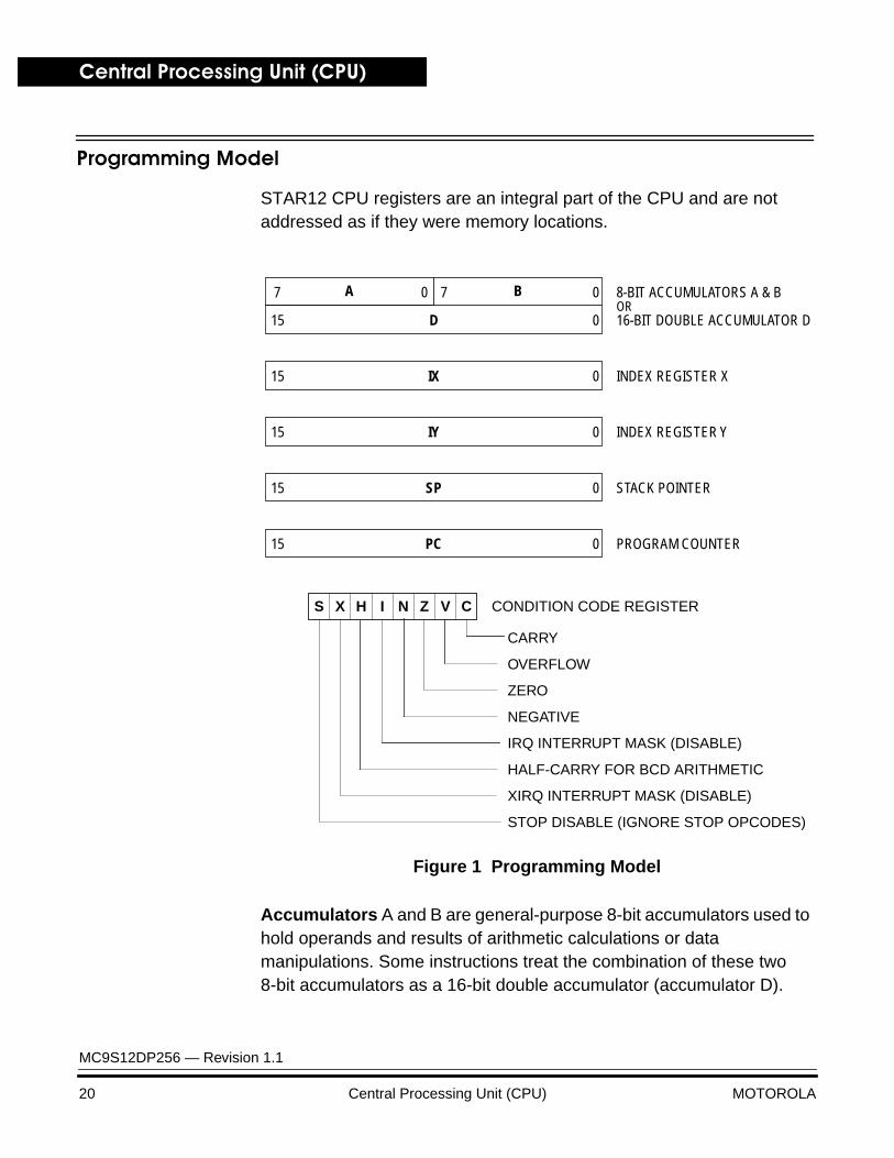
STAR12 CPU registers are an integral part of the CPU and are not addressed as if they were memory locations.
Figure 1 Programming Model
Accumulators
A and B are general-purpose 8-bit accumulators used to hold operands and results of arithmetic calculations or data manipulations. Some instructions treat the combination of these two 8-bit accumulators as a 16-bit double accumulator (accumulator D).
7
15
15
15
15
15
D
IX
IY
SP
PC
A B 0
0
0
0
0
0
70 8-BIT ACCUMULATORS A & B
16-BIT DOUBLE ACCUMULATOR D
INDEX REGISTER X
INDEX REGISTER Y
STACK POINTER
PROGRAM COUNTER
OR
NS X H I Z V C CONDITION CODE REGISTER
STOP DISABLE (IGNORE STOP OPCODES)
CARRY
OVERFLOW
ZERO
NEGATIVE
IRQ INTERRUPT MASK (DISABLE)
HALF-CARRY FOR BCD ARITHMETIC
XIRQ INTERRUPT MASK (DISABLE)
Central Processing Unit (CPU)Programming Model
MC9S12DP256 — Revision 1.1
MOTOROLA Central Processing Unit (CPU) 21
Index registers
X and Y are used for indexed addressing mode. In the indexed addressing mode, the contents of a 16-bit index register are added to 5-bit, 9-bit, or 16-bit constants or the content of an accumulator to form the effective address of the operand to be used in the instruction.
Stack and Memory Layout
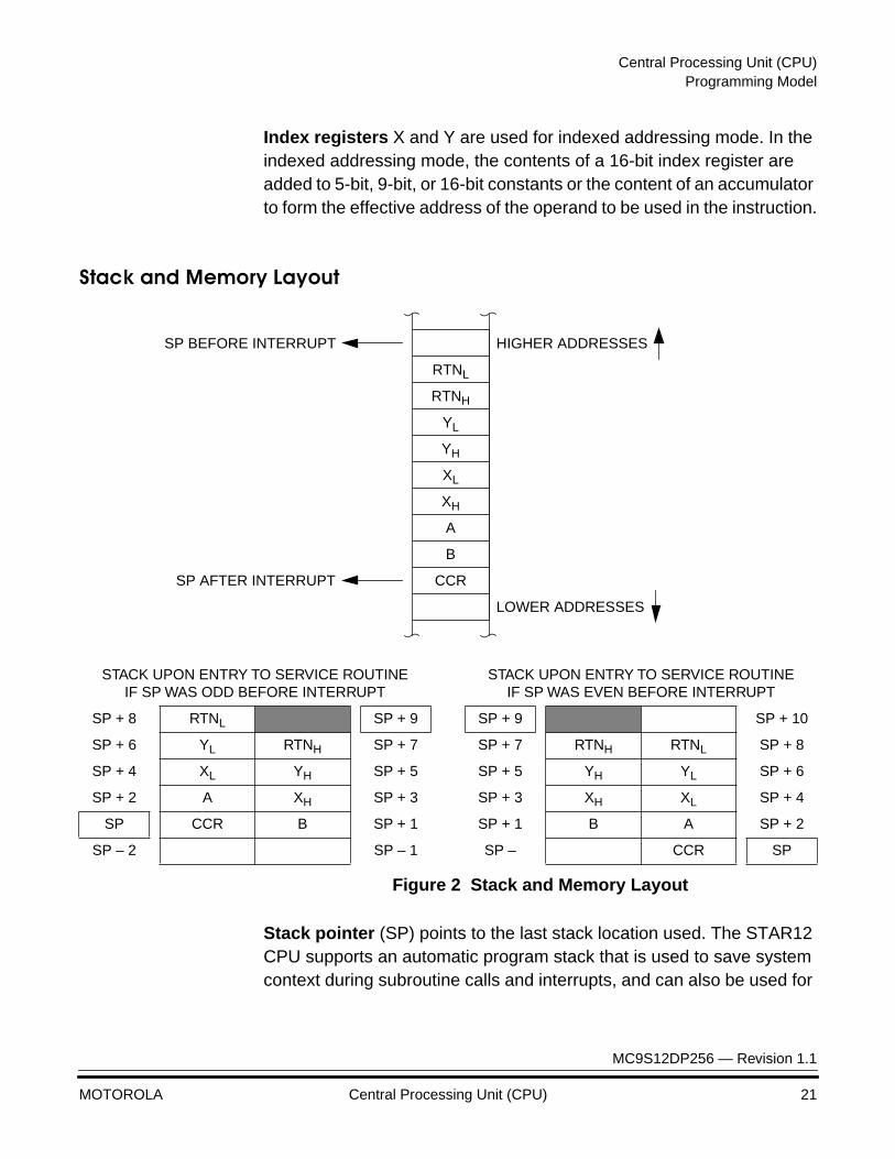
Figure 2 Stack and Memory Layout
Stack pointer
(SP) points to the last stack location used. The STAR12 CPU supports an automatic program stack that is used to save system context during subroutine calls and interrupts, and can also be used for
HIGHER ADDRESSES
LOWER ADDRESSES
RTNL
RTNH
YL
YH
XL
XH
A
B
CCR
SP BEFORE INTERRUPT
SP AFTER INTERRUPT
STACK UPON ENTRY TO SERVICE ROUTINEIF SP WAS ODD BEFORE INTERRUPT
STACK UPON ENTRY TO SERVICE ROUTINEIF SP WAS EVEN BEFORE INTERRUPT
SP + 8 RTN
L
SP + 9 SP + 9 SP + 10
SP + 6 Y
L
RTN
H
SP + 7 SP + 7 RTN
H
RTN
L
SP + 8
SP + 4 X
L
YH SP + 5 SP + 5 YH YL SP + 6
SP + 2 A XH SP + 3 SP + 3 XH XL SP + 4
SP CCR B SP + 1 SP + 1 B A SP + 2
SP – 2 SP – 1 SP – CCR SP
Central Processing Unit (CPU)
MC9S12DP256 — Revision 1.1
22 Central Processing Unit (CPU) MOTOROLA
temporary storage of data. The stack pointer can also be used in all indexed addressing modes.
Program counter is a 16-bit register that holds the address of the next instruction to be executed. The program counter can be used in all indexed addressing modes except autoincrement/decrement.
Condition Code Register (CCR) contains five status indicators, two interrupt masking bits, and a STOP disable bit. The five flags are half carry (H), negative (N), zero (Z), overflow (V), and carry/borrow (C). The half-carry flag is used only for BCD arithmetic operations. The N, Z, V, and C status bits allow for branching based on the results of a previous operation.
Data Types
The STAR12 CPU supports the following data types:
• Bit data
• 8-bit and 16-bit signed and unsigned integers
• 16-bit unsigned fractions
• 16-bit addresses
A byte is eight bits wide and can be accessed at any byte location. A word is composed of two consecutive bytes with the most significant byte at the lower value address. There are no special requirements for alignment of instructions or operands.
Central Processing Unit (CPU)Addressing Modes
MC9S12DP256 — Revision 1.1
MOTOROLA Central Processing Unit (CPU) 23
Addressing Modes
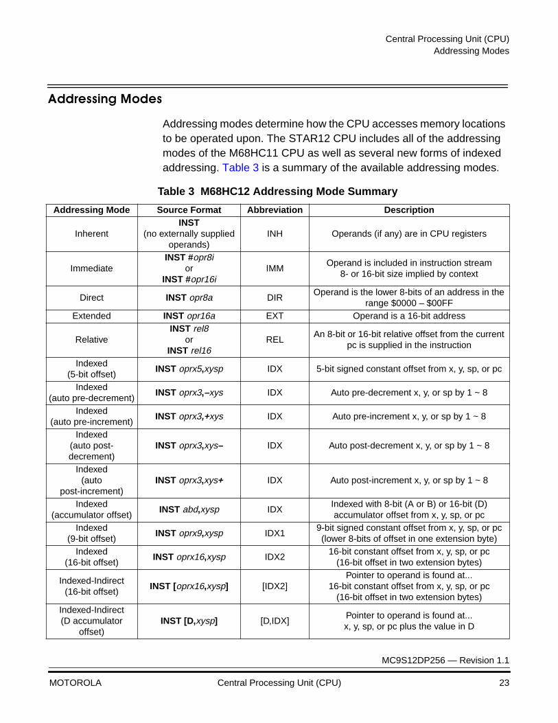
Addressing modes determine how the CPU accesses memory locations to be operated upon. The STAR12 CPU includes all of the addressing modes of the M68HC11 CPU as well as several new forms of indexed addressing. Table 3 is a summary of the available addressing modes.
Table 3 M68HC12 Addressing Mode Summary
Addressing Mode Source Format Abbreviation Description
InherentINST
(no externally supplied operands)
INH Operands (if any) are in CPU registers
ImmediateINST #opr8i
orINST #opr16i
IMMOperand is included in instruction stream
8- or 16-bit size implied by context
Direct INST opr8a DIROperand is the lower 8-bits of an address in the
range $0000 – $00FFExtended INST opr16a EXT Operand is a 16-bit address
RelativeINST rel8
orINST rel16
RELAn 8-bit or 16-bit relative offset from the current
pc is supplied in the instruction
Indexed(5-bit offset)
INST oprx5,xysp IDX 5-bit signed constant offset from x, y, sp, or pc
Indexed(auto pre-decrement)
INST oprx3,–xys IDX Auto pre-decrement x, y, or sp by 1 ~ 8
Indexed(auto pre-increment)
INST oprx3,+xys IDX Auto pre-increment x, y, or sp by 1 ~ 8
Indexed(auto post-decrement)
INST oprx3,xys– IDX Auto post-decrement x, y, or sp by 1 ~ 8
Indexed(auto
post-increment)INST oprx3,xys+ IDX Auto post-increment x, y, or sp by 1 ~ 8
Indexed(accumulator offset)
INST abd,xysp IDXIndexed with 8-bit (A or B) or 16-bit (D) accumulator offset from x, y, sp, or pc
Indexed(9-bit offset)
INST oprx9,xysp IDX19-bit signed constant offset from x, y, sp, or pc (lower 8-bits of offset in one extension byte)
Indexed(16-bit offset)
INST oprx16,xysp IDX216-bit constant offset from x, y, sp, or pc
(16-bit offset in two extension bytes)
Indexed-Indirect(16-bit offset)
INST [oprx16,xysp] [IDX2]Pointer to operand is found at...
16-bit constant offset from x, y, sp, or pc(16-bit offset in two extension bytes)
Indexed-Indirect(D accumulator
offset)INST [D,xysp] [D,IDX]
Pointer to operand is found at...x, y, sp, or pc plus the value in D

Central Processing Unit (CPU)
MC9S12DP256 — Revision 1.1
24 Central Processing Unit (CPU) MOTOROLA
Indexed Addressing Modes
The STAR12 CPU indexed modes reduce execution time and eliminate code size penalties for using the Y index register. STAR12 CPU indexed addressing uses a postbyte plus zero, one, or two extension bytes after the instruction opcode. The postbyte and extensions do the following tasks:
• Specify which index register is used.
• Determine whether a value in an accumulator is used as an offset.
• Enable automatic pre- or post-increment or decrement
• Specify use of 5-bit, 9-bit, or 16-bit signed offsets. Table 4 Summary of Indexed Operations
PostbyteCode (xb)
Source CodeSyntax Comments
rr0nnnnn,rn,r–n,r
5-bit constant offset n = –16 to +15rr can specify X, Y, SP, or PC
111rr0zsn,r–n,r
Constant offset (9- or 16-bit signed)z-0 = 9-bit with sign in LSB of postbyte(s)1 = 16-bitif z = s = 1, 16-bit offset indexed-indirect (see below)rr can specify X, Y, SP, or PC
111rr011 [n,r]16-bit offset indexed-indirect
rr can specify X, Y, SP, or PC
rr1pnnnnn,–r n,+rn,r– n,r+
Auto pre-decrement/increment or Auto post-decrement/increment; p = pre-(0) or post-(1), n = –8 to –1, +1 to +8rr can specify X, Y, or SP (PC not a valid choice)
111rr1aaA,rB,rD,r
Accumulator offset (unsigned 8-bit or 16-bit)aa-00 = A01 = B10 = D (16-bit)11 = see accumulator D offset indexed-indirectrr can specify X, Y, SP, or PC
111rr111 [D,r]Accumulator D offset indexed-indirect
rr can specify X, Y, SP, or PC
Central Processing Unit (CPU)Opcodes and Operands
MC9S12DP256 — Revision 1.1
MOTOROLA Central Processing Unit (CPU) 25
Opcodes and Operands
The STAR12 CPU uses 8-bit opcodes. Each opcode identifies a particular instruction and associated addressing mode to the CPU. Several opcodes are required to provide each instruction with a range of addressing capabilities.
Only 256 opcodes would be available if the range of values were restricted to the number that can be represented by 8-bit binary numbers. To expand the number of opcodes, a second page is added to the opcode map. Opcodes on the second page are preceded by an additional byte with the value $18.
To provide additional addressing flexibility, opcodes can also be followed by a postbyte or extension bytes. Postbytes implement certain forms of indexed addressing, transfers, exchanges, and loop primitives. Extension bytes contain additional program information such as addresses, offsets, and immediate data.
Central Processing Unit (CPU)
MC9S12DP256 — Revision 1.1
26 Central Processing Unit (CPU) MOTOROLA
Instruction Set Summary
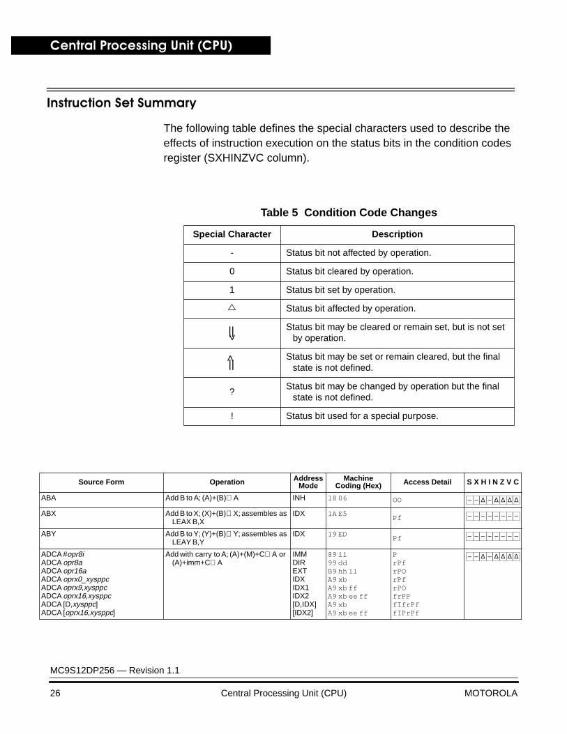
The following table defines the special characters used to describe the effects of instruction execution on the status bits in the condition codes register (SXHINZVC column).
Table 5 Condition Code Changes
Special Character Description
- Status bit not affected by operation.
0 Status bit cleared by operation.
1 Status bit set by operation.
Status bit affected by operation.
Status bit may be cleared or remain set, but is not set by operation.
Status bit may be set or remain cleared, but the final state is not defined.
?Status bit may be changed by operation but the final
state is not defined.
! Status bit used for a special purpose.
Source Form Operation AddressMode
Machine Coding (Hex) Access Detail S X H I N Z V C
ABA Add B to A; (A)+(B)⇒ A INH 18 06 OO
ABX Add B to X; (X)+(B)⇒ X; assembles as LEAX B,X
IDX 1A E5Pf
ABY Add B to Y; (Y)+(B)⇒ Y; assembles as LEAY B,Y
IDX 19 EDPf
ADCA #opr8iADCA opr8aADCA opr16aADCA oprx0_xysppcADCA oprx9,xysppcADCA oprx16,xysppcADCA [D,xysppc]ADCA [oprx16,xysppc]
Add with carry to A; (A)+(M)+C⇒ A or (A)+imm+C⇒ A
IMMDIREXTIDXIDX1IDX2[D,IDX][IDX2]
89 ii99 ddB9 hh llA9 xbA9 xb ffA9 xb ee ffA9 xbA9 xb ee ff
PrPfrPOrPfrPOfrPPfIfrPffIPrPf
– – ∆ – ∆ ∆ ∆ ∆
– – – – – – – –
– – – – – – – –
– – ∆ – ∆ ∆ ∆ ∆
||>
||>
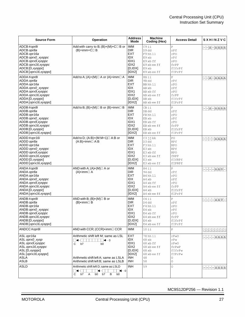
Central Processing Unit (CPU)Instruction Set Summary
MC9S12DP256 — Revision 1.1
MOTOROLA Central Processing Unit (CPU) 27
ADCB #opr8iADCB opr8aADCB opr16aADCB oprx0_xysppcADCB oprx9,xysppcADCB oprx16,xysppcADCB [D,xysppc]ADCB [oprx16,xysppc]
Add with carry to B; (B)+(M)+C⇒ B or (B)+imm+C⇒ B
IMMDIREXTIDXIDX1IDX2[D,IDX][IDX2]
C9 iiD9 ddF9 hh llE9 xbE9 xb ffE9 xb ee ffE9 xbE9 xb ee ff
PrPfrPOrPfrPOfrPPfIfrPffIPrPf
ADDA #opr8iADDA opr8aADDA opr16aADDA oprx0_xysppcADDA oprx9,xysppcADDA oprx16,xysppcADDA [D,xysppc]ADDA [oprx16,xysppc]
Add to A; (A)+(M)⇒ A or (A)+imm⇒ A IMMDIREXTIDXIDX1IDX2[D,IDX][IDX2]
8B ii9B ddBB hh llAB xbAB xb ffAB xb ee ffAB xbAB xb ee ff
PrPfrPOrPfrPOfrPPfIfrPffIPrPf
ADDB #opr8iADDB opr8aADDB opr16aADDB oprx0_xysppcADDB oprx9,xysppcADDB oprx16,xysppcADDB [D,xysppc]ADDB [oprx16,xysppc]
Add to B; (B)+(M)⇒ B or (B)+imm⇒ B IMMDIREXTIDXIDX1IDX2[D,IDX][IDX2]
CB iiDB ddFB hh llEB xbEB xb ffEB xb ee ffEB xbEB xb ee ff
PrPfrPOrPfrPOfrPPfIfrPffIPrPf
ADDD #opr16iADDD opr8aADDD opr16aADDD oprx0_xysppcADDD oprx9,xysppcADDD oprx16,xysppcADDD [D,xysppc]ADDD [oprx16,xysppc]
Add to D; (A:B)+(M:M+1)⇒ A:B or (A:B)+imm⇒ A:B
IMMDIREXTIDXIDX1IDX2[D,IDX][IDX2]
C3 jj kkD3 ddF3 hh llE3 xbE3 xb ffE3 xb ee ffE3 xbE3 xb ee ff
PORPfRPORPfRPOfRPPfIfRPffIPRPf
ANDA #opr8iANDA opr8aANDA opr16aANDA oprx0_xysppcANDA oprx9,xysppcANDA oprx16,xysppcANDA [D,xysppc]ANDA [oprx16,xysppc]
AND with A; (A)• (M)⇒ A or (A)• imm⇒ A
IMMDIREXTIDXIDX1IDX2[D,IDX][IDX2]
84 ii94 ddB4 hh llA4 xbA4 xb ffA4 xb ee ffA4 xbA4 xb ee ff
PrPfrPOrPfrPOfrPPfIfrPffIPrPf
ANDB #opr8iANDB opr8aANDB opr16aANDB oprx0_xysppcANDB oprx9,xysppcANDB oprx16,xysppcANDB [D,xysppc]ANDB [oprx16,xysppc]
AND with B; (B)• (M)⇒ B or (B)• imm⇒ B
IMMDIREXTIDXIDX1IDX2[D,IDX][IDX2]
C4 iiD4 ddF4 hh llE4 xbE4 xb ffE4 xb ee ffE4 xbE4 xb ee ff
PrPfrPOrPfrPOfrPPfIfrPffIPrPf
ANDCC #opr8i AND with CCR; (CCR)• imm⇒ CCR IMM 10 ii P
ASL opr16aASL oprx0_xyspASL oprx9,xysppcASL oprx16,xysppcASL [D,xysppc]ASL [oprx16,xysppc]ASLAASLB
Arithmetic shift left M; same as LSL
Arithmetic shift left A; same as LSLAArithmetic shift left B; same as LSLB
EXTIDXIDX1IDX2[D,IDX][IDX2]INHINH
78 hh ll68 xb68 xb ff68 xb ee ff68 xb68 xb ee ff4858
rPwOrPwrPwOfrPwPfIfrPwfIPrPwOO
ASLD Arithmetic shift left D; same as LSLD INH 59 O
Source Form Operation AddressMode
Machine Coding (Hex) Access Detail S X H I N Z V C
– – ∆ – ∆ ∆ ∆ ∆
– – ∆ – ∆ ∆ ∆ ∆
– – ∆ – ∆ ∆ ∆ ∆
– – – – ∆ ∆ ∆ ∆
– – – – ∆ ∆ 0 –
– – – – ∆ ∆ 0 –
⇓ ⇓ ⇓ ⇓ ⇓ ⇓ ⇓ ⇓
C0
b7 b0
– – – – ∆ ∆ ∆ ∆
C0
b7 b0A Bb7b0
– – – – ∆ ∆ ∆ ∆
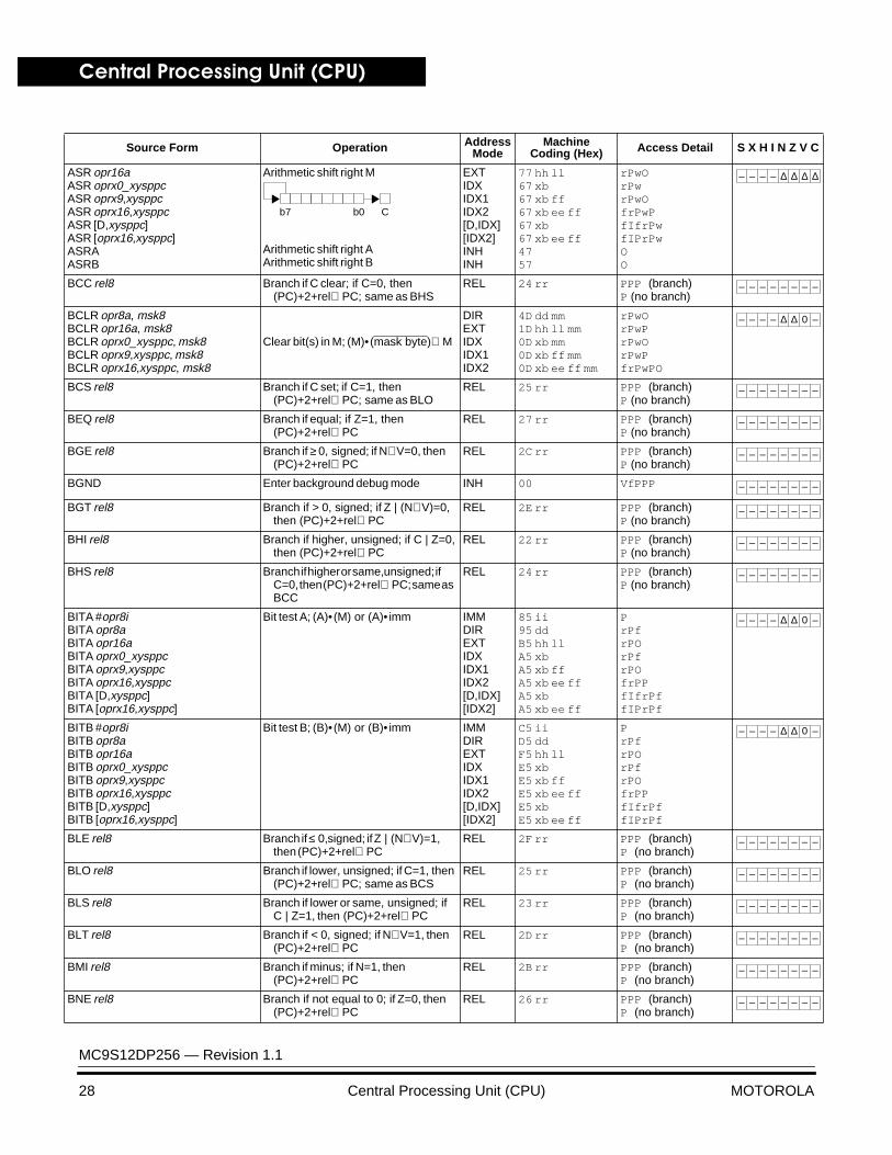
Central Processing Unit (CPU)
MC9S12DP256 — Revision 1.1
28 Central Processing Unit (CPU) MOTOROLA
ASR opr16aASR oprx0_xysppcASR oprx9,xysppcASR oprx16,xysppcASR [D,xysppc]ASR [oprx16,xysppc]ASRAASRB
Arithmetic shift right M
Arithmetic shift right AArithmetic shift right B
EXTIDXIDX1IDX2[D,IDX][IDX2]INHINH
77 hh ll67 xb67 xb ff67 xb ee ff67 xb67 xb ee ff4757
rPwOrPwrPwOfrPwPfIfrPwfIPrPwOO
BCC rel8 Branch if C clear; if C=0, then (PC)+2+rel⇒ PC; same as BHS
REL 24 rr PPP (branch)P (no branch)
BCLR opr8a, msk8BCLR opr16a, msk8BCLR oprx0_xysppc, msk8BCLR oprx9,xysppc, msk8BCLR oprx16,xysppc, msk8
Clear bit(s) in M; (M)• (mask byte)⇒ M
DIREXTIDXIDX1IDX2
4D dd mm1D hh ll mm0D xb mm0D xb ff mm0D xb ee ff mm
rPwOrPwPrPwOrPwPfrPwPO
BCS rel8 Branch if C set; if C=1, then (PC)+2+rel⇒ PC; same as BLO
REL 25 rr PPP (branch)P (no branch)
BEQ rel8 Branch if equal; if Z=1, then (PC)+2+rel⇒ PC
REL 27 rr PPP (branch)P (no branch)
BGE rel8 Branch if ≥ 0, signed; if N⊕ V=0, then (PC)+2+rel⇒ PC
REL 2C rr PPP (branch)P (no branch)
BGND Enter background debug mode INH 00 VfPPP
BGT rel8 Branch if > 0, signed; if Z | (N⊕ V)=0, then (PC)+2+rel⇒ PC
REL 2E rr PPP (branch)P (no branch)
BHI rel8 Branch if higher, unsigned; if C | Z=0, then (PC)+2+rel⇒ PC
REL 22 rr PPP (branch)P (no branch)
BHS rel8 Branch if higher or same, unsigned; if C=0, then (PC)+2+rel⇒ PC; same as BCC
REL 24 rr PPP (branch)P (no branch)
BITA #opr8iBITA opr8aBITA opr16aBITA oprx0_xysppcBITA oprx9,xysppcBITA oprx16,xysppcBITA [D,xysppc]BITA [oprx16,xysppc]
Bit test A; (A)• (M) or (A)• imm IMMDIREXTIDXIDX1IDX2[D,IDX][IDX2]
85 ii95 ddB5 hh llA5 xbA5 xb ffA5 xb ee ffA5 xbA5 xb ee ff
PrPfrPOrPfrPOfrPPfIfrPffIPrPf
BITB #opr8iBITB opr8aBITB opr16aBITB oprx0_xysppcBITB oprx9,xysppcBITB oprx16,xysppcBITB [D,xysppc]BITB [oprx16,xysppc]
Bit test B; (B)• (M) or (B)• imm IMMDIREXTIDXIDX1IDX2[D,IDX][IDX2]
C5 iiD5 ddF5 hh llE5 xbE5 xb ffE5 xb ee ffE5 xbE5 xb ee ff
PrPfrPOrPfrPOfrPPfIfrPffIPrPf
BLE rel8 Branch if ≤ 0, signed; if Z | (N⊕ V)=1, then (PC)+2+rel⇒ PC
REL 2F rr PPP (branch)P (no branch)
BLO rel8 Branch if lower, unsigned; if C=1, then (PC)+2+rel⇒ PC; same as BCS
REL 25 rr PPP (branch)P (no branch)
BLS rel8 Branch if lower or same, unsigned; if C | Z=1, then (PC)+2+rel⇒ PC
REL 23 rr PPP (branch)P (no branch)
BLT rel8 Branch if < 0, signed; if N⊕ V=1, then (PC)+2+rel⇒ PC
REL 2D rr PPP (branch)P (no branch)
BMI rel8 Branch if minus; if N=1, then (PC)+2+rel⇒ PC
REL 2B rr PPP (branch)P (no branch)
BNE rel8 Branch if not equal to 0; if Z=0, then (PC)+2+rel⇒ PC
REL 26 rr PPP (branch)P (no branch)
Source Form Operation AddressMode
Machine Coding (Hex) Access Detail S X H I N Z V C
Cb7 b0
– – – – ∆ ∆ ∆ ∆
– – – – – – – –
– – – – ∆ ∆ 0 –
– – – – – – – –
– – – – – – – –
– – – – – – – –
– – – – – – – –
– – – – – – – –
– – – – – – – –
– – – – – – – –
– – – – ∆ ∆ 0 –
– – – – ∆ ∆ 0 –
– – – – – – – –
– – – – – – – –
– – – – – – – –
– – – – – – – –
– – – – – – – –
– – – – – – – –

Central Processing Unit (CPU)Instruction Set Summary
MC9S12DP256 — Revision 1.1
MOTOROLA Central Processing Unit (CPU) 29
BPL rel8 Branch if plus; if N=0, then (PC)+2+rel⇒ PC
REL 2A rr PPP (branch)P (no branch)
BRA rel8 Branch always REL 20 rr PPP
BRCLR opr8a, msk8, rel8BRCLR opr16a, msk8, rel8BRCLR oprx0_xysppc, msk8, rel8BRCLR oprx9,xysppc, msk8, rel8BRCLR oprx16,xysppc, msk8, rel8
Branch if bit(s) clear; if (M)• (mask byte)=0, then (PC)+2+rel⇒ PC
DIREXTIDXIDX1IDX2
4F dd mm rr1F hh ll mm rr0F xb mm rr0F xb ff mm rr0F xb ee ff mm rr
rPPPrfPPPrPPPrfPPPPrfPPP
BRN rel8 Branch never REL 21 rr P
BRSET opr8, msk8, rel8BRSET opr16a, msk8, rel8BRSET oprx0_xysppc, msk8, rel8BRSET oprx9,xysppc, msk8, rel8BRSET oprx16,xysppc, msk8, rel8
Branch if bit(s) set; if (M)• (mask byte)=0, then (PC)+2+rel⇒ PC
DIREXTIDXIDX1IDX2
4E dd mm rr1E hh ll mm rr0E xb mm rr0E xb ff mm rr0E xb ee ff mm rr
rPPPrfPPPrPPPrfPPPPrfPPP
BSET opr8, msk8BSET opr16a, msk8BSET oprx0_xysppc, msk8BSET oprx9,xysppc, msk8BSET oprx16,xysppc, msk8
Set bit(s) in M; (M) | (mask byte)⇒ M DIREXTIDXIDX1IDX2
4C dd mm1C hh ll mm0C xb mm0C xb ff mm0C xb ee ff mm
rPwOrPwPrPwOrPwPfrPwPO
BSR rel8 Branch to subroutine; (SP)–2⇒ SP;RTNH:RTNL⇒ MSP:MSP+1;(PC)+2+rel⇒ PC
REL 07 rr SPPP
BVC rel8 Branch if V clear; if V=0, then (PC)+2+rel⇒ PC
REL 28 rr PPP (branch)P (no branch)
BVS rel8 Branch if V set; if V=1, then (PC)+2+rel⇒ PC
REL 29 rr PPP (branch)P (no branch)
CALL opr16a, pageCALL oprx0_xysppc, pageCALL oprx9,xysppc, pageCALL oprx16,xysppc, pageCALL [D,xysppc]CALL [oprx16, xysppc]
Call subroutine in expanded memory; (SP)–2⇒ SP;
RTNH:RTNL⇒ MSP:MSP+1;(SP)–1⇒ SP; (PPG)⇒ MSP;pg⇒ PPAGE register;subroutine address⇒ PC
EXTIDXIDX1IDX2[D,IDX][IDX2]
4A hh ll pg4B xb pg4B xb ff pg4B xb ee ff pg4B xb4B xb ee ff
gnSsPPPgnSsPPPgnSsPPPfgnSsPPPfIignSsPPPfIignSsPPP
CBA Compare A to B; (A)–(B) INH 18 17 OO
CLC Clear C; assembles as ANDCC #$FE IMM 10 FE P
CLI Clear I; assembles as ANDCC #$EF IMM 10 EF P
CLR opr16aCLR oprx0_xysppcCLR oprx9,xysppcCLR oprx16,xysppcCLR [D,xysppc]CLR [oprx16,xysppc]CLRACLRB
Clear M; $00⇒ M
Clear A; $00⇒ AClear B; $00⇒ B
EXTIDXIDX1IDX2[D,IDX][IDX2]INHINH
79 hh ll69 xb69 xb ff69 xb ee ff69 xb69 xb ee ff87C7
PwOPwPwOPwPPIfwPIPwOO
CLV Clear V; assembles as ANDCC #$FD IMM 10 FD P
CMPA #opr8iCMPA opr8aCMPA opr16aCMPA oprx0_xysppcCMPA oprx9,xysppcCMPA oprx16,xysppcCMPA [D,xysppc]CMPA [oprx16,xysppc]
Compare A; (A)–(M) or (A)–imm IMMDIREXTIDXIDX1IDX2[D,IDX][IDX2]
81 ii91 ddB1 hh llA1 xbA1 xb ffA1 xb ee ffA1 xb A1 xb ee ff
PrPfrPOrPfrPOfrPPfIfrPffIPrPf
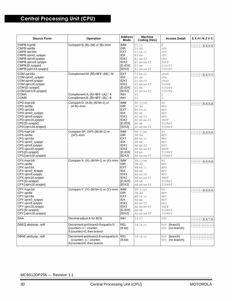
Source Form Operation AddressMode
Machine Coding (Hex) Access Detail S X H I N Z V C
– – – – – – – –
– – – – – – – –
– – – – – – – –
– – – – – – – –
– – – – – – – –
– – – – ∆ ∆ 0 –
– – – – – – – –
– – – – – – – –
– – – – – – – –
– – – – – – – –
– – – – ∆ ∆ ∆ ∆
– – – – – – – 0
– – – 0 – – – –
– – – – 0 1 0 0
– – – – – – 0 –
– – – – ∆ ∆ ∆ ∆
Central Processing Unit (CPU)
MC9S12DP256 — Revision 1.1
30 Central Processing Unit (CPU) MOTOROLA
CMPB #opr8iCMPB opr8aCMPB opr16aCMPB oprx0_xysppcCMPB oprx9,xysppcCMPB oprx16,xysppcCMPB [D,xysppc]CMPB [oprx16,xysppc]
Compare B; (B)–(M) or (B)–imm IMMDIREXTIDXIDX1IDX2[D,IDX][IDX2]
C1 iiD1 ddF1 hh llE1 xbE1 xb ffE1 xb ee ffE1 xbE1 xb ee ff
PrPfrPOrPfrPOfrPPfIfrPffIPrPf
COM opr16aCOM oprx0_xysppcCOM oprx9,xysppcCOM oprx16,xysppcCOM [D,xysppc]COM [oprx16,xysppc]COMACOMB
Complement M; (M)=$FF–(M)⇒ M
Complement A; (A)=$FF–(A)⇒ AComplement B; (B)=$FF–(B)⇒ B
EXTIDXIDX1IDX2[D,IDX][IDX2]INHINH
71 hh ll61 xb61 xb ff61 xb ee ff61 xb61 xb ee ff4151
rPwOrPwrPwOfrPwPfIfrPwfIPrPwOO
CPD #opr16iCPD opr8aCPD opr16aCPD oprx0_xysppcCPD oprx9,xysppcCPD oprx16,xysppcCPD [D,xysppc]CPD [oprx16,xysppc]
Compare D; (A:B)–(M:M+1) or (A:B)–imm
IMMDIREXTIDXIDX1IDX2[D,IDX][IDX2]
8C jj kk9C ddBC hh llAC xbAC xb ffAC xb ee ffAC xbAC xb ee ff
PORPfRPORPfRPOfRPPfIfRPffIPRPf
CPS #opr16iCPS opr8aCPS opr16aCPS oprx0_xysppcCPS oprx9,xysppcCPS oprx16,xysppcCPS [D,xysppc]CPS [oprx16,xysppc]
Compare SP; (SP)–(M:M+1) or (SP)–imm
IMMDIREXTIDXIDX1IDX2[D,IDX][IDX2]
8F jj kk9F ddBF hh llAF xbAF xb ffAF xb ee ffAF xbAF xb ee ff
PORPfRPORPfRPOfRPPfIfRPffIPRPf
CPX #opr16iCPX opr8aCPX opr16aCPX oprx0_xysppcCPX oprx9,xysppcCPX oprx16,xysppcCPX [D,xysppc]CPX [oprx16,xysppc]
Compare X; (X)–(M:M+1) or (X)–imm IMMDIREXTIDXIDX1IDX2[D,IDX][IDX2]
8E jj kk9E ddBE hh llAE xbAE xb ffAE xb ee ffAE xbAE xb ee ff
PORPfRPORPfRPOfRPPfIfRPffIPRPf
CPY #opr16iCPY opr8aCPY opr16aCPY oprx0_xysppcCPY oprx9,xysppcCPY oprx16,xysppcCPY [D,xysppc]CPY [oprx16,xysppc]
Compare Y; (Y)–(M:M+1) or (Y)–imm IMMDIREXTIDXIDX1IDX2[D,IDX][IDX2]
8D jj kk9D ddBD hh llAD xbAD xb ffAD xb ee ffAD xbAD xb ee ff
PORPfRPORPfRPOfRPPfIfRPffIPRPf
DAA Decimal adjust A for BCD INH 18 07 OfO
DBEQ abdxysp, rel9 Decrement and branch if equal to 0;(counter)–1⇒ counter;if (counter)=0, then branch
REL(9-bit)
04 lb rr PPP (branch)PPO (no branch)
DBNE abdxysp, rel9 Decrement and branch if not equal to 0; (counter)–1⇒ counter;
if (counter)≠0, then branch
REL(9-bit)
04 lb rr PPP (branch)PPO (no branch)
Source Form Operation AddressMode
Machine Coding (Hex) Access Detail S X H I N Z V C
– – – – ∆ ∆ ∆ ∆
– – – – ∆ ∆ 0 1
– – – – ∆ ∆ ∆ ∆
– – – – ∆ ∆ ∆ ∆
– – – – ∆ ∆ ∆ ∆
– – – – ∆ ∆ ∆ ∆
– – – – ∆ ∆ ? ∆
– – – – – – – –
– – – – – – – –

Central Processing Unit (CPU)Instruction Set Summary
MC9S12DP256 — Revision 1.1
MOTOROLA Central Processing Unit (CPU) 31
DEC opr16aDEC oprx0_xysppcDEC oprx9,xysppcDEC oprx16,xysppcDEC [D,xysppc]DEC [oprx16,xysppc]DECADECB
Decrement M; (M)–1⇒ M
Decrement A; (A)–1⇒ ADecrement B; (B)–1⇒ B
EXTIDXIDX1IDX2[D,IDX][IDX2]INHINH
73 hh ll63 xb63 xb ff63 xb ee ff63 xb63 xb ee ff4353
rPwOrPwrPwOfrPwPfIfrPwfIPrPwOO
DES Decrement SP; (SP)–1⇒ SP; assembles as LEAS –1,SP
IDX 1B 9F Pf
DEX Decrement X; (X)–1⇒ X INH 09 O
DEY Decrement Y; (Y)–1⇒ Y INH 03 O
EDIV Extended divide, unsigned; 32 by 16 to 16-bit; (Y:D)÷(X)⇒ Y; remainder⇒ D
INH 11 ffffffffffO
EDIVS Extended divide, signed; 32 by 16 to 16-bit; (Y:D)÷(X)⇒ Y; remainder⇒ D
INH 18 14 OffffffffffO
EMACS opr16a Extended multiply and accumulate,signed; (MX:MX+1)×(MY:MY+1)+(M~M+3)⇒ M~M+3; 16 by 16 to 32-bit
Special 18 12 hh ll ORROfffRRfWWP
EMAXD oprx0_xysppcEMAXD oprx9,xysppcEMAXD oprx16,xysppcEMAXD [D,xysppc]EMAXD [oprx16,xysppc]
Extended maximum in D; put larger of 2 unsigned 16-bit values in D;
MAX[(D), (M:M+1)]⇒ D;N, Z, V, C bits reflect result of internalcompare [(D)–(M:M+1)]
IDXIDX1IDX2[D,IDX][IDX2]
18 1A xb18 1A xb ff18 1A xb ee ff18 1A xb18 1A xb ee ff
ORPfORPOOfRPPOfIfRPfOfIPRPf
EMAXM oprx0_xysppcEMAXM oprx9,xysppcEMAXM oprx16,xysppcEMAXM [D,xysppc]EMAXM [oprx16,xysppc]
Extended maximum in M; put larger of 2 unsigned 16-bit values in M;
MAX[(D), (M:M+1)]⇒ M:M+1;N, Z, V, C bits reflect result of internalcompare [(D)–(M:M+1)]
IDXIDX1IDX2[D,IDX][IDX2]
18 1E xb18 1E xb ff18 1E xb ee ff18 1E xb18 1E xb ee ff
ORPWORPWOOfRPWPOfIfRPWOfIPRPW
EMIND oprx0_xysppcEMIND oprx9,xysppcEMIND oprx16,xysppcEMIND [D,xysppc]EMIND [oprx16,xysppc]
Extended minimum in D; put smaller of 2 unsigned 16-bit values in D;
MIN[(D), (M:M+1)]⇒ D;N, Z, V, C bits reflect result ofinternal compare [(D)–(M:M+1)]
IDXIDX1IDX2[D,IDX][IDX2]
18 1B xb18 1B xb ff18 1B xb ee ff18 1B xb18 1B xb ee ff
ORPfORPOOfRPPOfIfRPfOfIPRPf
EMINM oprx0_xysppcEMINM oprx9,xysppcEMINM oprx16,xysppcEMINM [D,xysppc]EMINM [oprx16,xysppc]
Extended minimum in M; put smaller of 2 unsigned 16-bit values in M;
MIN[(D), (M:M+1)]⇒ M:M+1;N, Z, V, C bits reflect result of internal
compare [(D)–(M:M+1)]
IDXIDX1IDX2[D,IDX][IDX2]
18 1F xb18 1F xb ff18 1F xb ee ff18 1F xb18 1F xb ee ff
ORPWORPWOOfRPWPOfIfRPWOfIPRPW
EMUL Extended multiply, unsigned;(D)×(Y)⇒ Y:D; 16 by 16 to 32-bit
INH 13 ffO
EMULS Extended multiply, signed;(D)×(Y)⇒ Y:D; 16 by 16 to 32-bit
INH 18 13 OfOOffO (if followed by
page 2 instruction)
EORA #opr8iEORA opr8aEORA opr16aEORA oprx0_xysppcEORA oprx9,xysppcEORA oprx16,xysppcEORA [D,xysppc]EORA [oprx16,xysppc]
Exclusive OR A; (A)⊕ (M)⇒ A or (A)⊕ imm⇒ A
IMMDIREXTIDXIDX1IDX2[D,IDX][IDX2]
88 ii98 ddB8 hh llA8 xbA8 xb ffA8 xb ee ffA8 xbA8 xb ee ff
PrPfrPOrPfrPOfrPPfIfrPffIPrPf
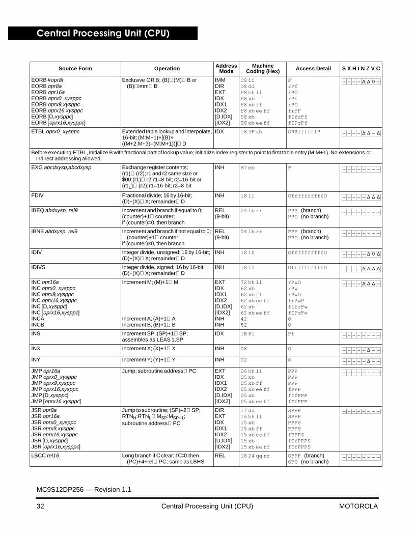
Source Form Operation AddressMode
Machine Coding (Hex) Access Detail S X H I N Z V C
– – – – ∆ ∆ ∆ –
– – – – – – – –
– – – – – ∆ – –
– – – – – ∆ – –
– – – – ∆ ∆ ∆ ∆
– – – – ∆ ∆ ∆ ∆
– – – – ∆ ∆ ∆ ∆
– – – – ∆ ∆ ∆ ∆
– – – – ∆ ∆ ∆ ∆
– – – – ∆ ∆ ∆ ∆
– – – – ∆ ∆ ∆ ∆
– – – – ∆ ∆ – ∆
– – – – ∆ ∆ – ∆
– – – – ∆ ∆ 0 –
Central Processing Unit (CPU)
MC9S12DP256 — Revision 1.1
32 Central Processing Unit (CPU) MOTOROLA
EORB #opr8iEORB opr8aEORB opr16aEORB oprx0_xysppcEORB oprx9,xysppcEORB oprx16,xysppcEORB [D,xysppc]EORB [oprx16,xysppc]
Exclusive OR B; (B)⊕ (M)⇒ B or (B)⊕ imm⇒ B
IMMDIREXTIDXIDX1IDX2[D,IDX][IDX2]
C8 iiD8 ddF8 hh llE8 xbE8 xb ffE8 xb ee ffE8 xbE8 xb ee ff
PrPfrPOrPfrPOfrPPfIfrPffIPrPf
ETBL oprx0_xysppc Extended table lookup and interpolate,16-bit; (M:M+1)+[(B)×((M+2:M+3)–(M:M+1))]⇒ D
IDX 18 3F xb ORRffffffP
Before executing ETBL, initialize B with fractional part of lookup value; initialize index register to point to first table entry (M:M+1). No extensions or indirect addressing allowed.
EXG abcdxysp,abcdxysp Exchange register contents;(r1)⇔(r2); r1 and r2 same size or$00:(r1)⇒ r2; r1=8-bit; r2=16-bit or(r1L)⇔(r2); r1=16-bit; r2=8-bit
INH B7 eb P
FDIV Fractional divide; 16 by 16-bit;(D)÷(X)⇒ X; remainder⇒ D
INH 18 11 OffffffffffO
IBEQ abdxysp, rel9 Increment and branch if equal to 0;(counter)+1⇒ counter;if (counter)=0, then branch
REL(9-bit)
04 lb rr PPP (branch)PPO (no branch)
IBNE abdxysp, rel9 Increment and branch if not equal to 0; (counter)+1⇒ counter;
if (counter)≠0, then branch
REL(9-bit)
04 lb rr PPP (branch)PPO (no branch)
IDIV Integer divide, unsigned; 16 by 16-bit;(D)÷(X)⇒ X; remainder⇒ D
INH 18 10 OffffffffffO
IDIVS Integer divide, signed; 16 by 16-bit;(D)÷(X)⇒ X; remainder⇒ D
INH 18 15 OffffffffffO
INC opr16aINC oprx0_xysppcINC oprx9,xysppcINC oprx16,xysppcINC [D,xysppc]INC [oprx16,xysppc]INCAINCB
Increment M; (M)+1⇒ M
Increment A; (A)+1⇒ AIncrement B; (B)+1⇒ B
EXTIDXIDX1IDX2[D,IDX][IDX2]INHINH
72 hh ll62 xb62 xb ff62 xb ee ff62 xb62 xb ee ff4252
rPwOrPwrPwOfrPwPfIfrPwfIPrPwOO
INS Increment SP; (SP)+1⇒ SP;assembles as LEAS 1,SP
IDX 1B 81 Pf
INX Increment X; (X)+1⇒ X INH 08 O
INY Increment Y; (Y)+1⇒ Y INH 02 O
JMP opr16aJMP oprx0_xysppcJMP oprx9,xysppcJMP oprx16,xysppcJMP [D,xysppc]JMP [oprx16,xysppc]
Jump; subroutine address⇒ PC EXTIDXIDX1IDX2[D,IDX][IDX2]
06 hh ll05 xb05 xb ff05 xb ee ff05 xb05 xb ee ff
PPPPPPPPPfPPPfIfPPPfIfPPP
JSR opr8aJSR opr16aJSR oprx0_xysppcJSR oprx9,xysppcJSR oprx16,xysppcJSR [D,xysppc]JSR [oprx16,xysppc]
Jump to subroutine; (SP)–2⇒ SP;RTNH:RTNL⇒ MSP:MSP+1;subroutine address⇒ PC
DIREXTIDXIDX1IDX2[D,IDX][IDX2]
17 dd16 hh ll15 xb15 xb ff15 xb ee ff15 xb15 xb ee ff
SPPPSPPPPPPSPPPSfPPPSfIfPPPSfIfPPPS
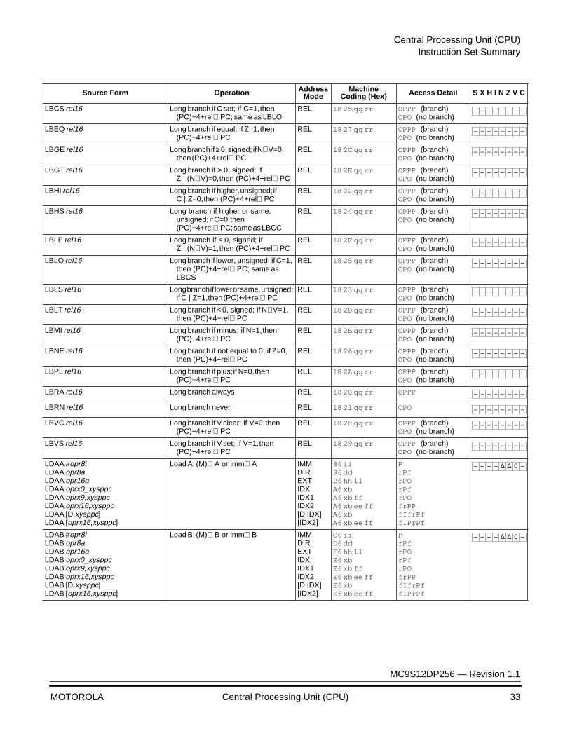
LBCC rel16 Long branch if C clear; if C=0, then (PC)+4+rel⇒ PC; same as LBHS
REL 18 24 qq rr OPPP (branch)OPO (no branch)
Source Form Operation AddressMode
Machine Coding (Hex) Access Detail S X H I N Z V C
– – – – ∆ ∆ 0 –
– – – – ∆ ∆ – ∆
– – – – – – – –
– – – – – ∆ ∆ ∆
– – – – – – – –
– – – – – – – –
– – – – – ∆ 0 ∆
– – – – ∆ ∆ ∆ ∆
– – – – ∆ ∆ ∆ –
– – – – – – – –
– – – – – ∆ – –
– – – – – ∆ – –
– – – – – – – –
– – – – – – – –
– – – – – – – –
Central Processing Unit (CPU)Instruction Set Summary
MC9S12DP256 — Revision 1.1
MOTOROLA Central Processing Unit (CPU) 33
LBCS rel16 Long branch if C set; if C=1, then (PC)+4+rel⇒ PC; same as LBLO
REL 18 25 qq rr OPPP (branch)OPO (no branch)
LBEQ rel16 Long branch if equal; if Z=1, then (PC)+4+rel⇒ PC
REL 18 27 qq rr OPPP (branch)OPO (no branch)
LBGE rel16 Long branch if ≥ 0, signed; if N⊕ V=0, then (PC)+4+rel⇒ PC
REL 18 2C qq rr OPPP (branch)OPO (no branch)
LBGT rel16 Long branch if > 0, signed; if Z | (N⊕ V)=0, then (PC)+4+rel⇒ PC
REL 18 2E qq rr OPPP (branch)OPO (no branch)
LBHI rel16 Long branch if higher, unsigned; if C | Z=0, then (PC)+4+rel⇒ PC
REL 18 22 qq rr OPPP (branch)OPO (no branch)
LBHS rel16 Long branch if higher or same, unsigned; if C=0, then (PC)+4+rel⇒ PC; same as LBCC
REL 18 24 qq rr OPPP (branch)OPO (no branch)
LBLE rel16 Long branch if ≤ 0, signed; if Z | (N⊕ V)=1, then (PC)+4+rel⇒ PC
REL 18 2F qq rr OPPP (branch)OPO (no branch)
LBLO rel16 Long branch if lower, unsigned; if C=1, then (PC)+4+rel⇒ PC; same as LBCS
REL 18 25 qq rr OPPP (branch)OPO (no branch)
LBLS rel16 Long branch if lower or same, unsigned; if C | Z=1, then (PC)+4+rel⇒ PC
REL 18 23 qq rr OPPP (branch)OPO (no branch)
LBLT rel16 Long branch if < 0, signed; if N⊕ V=1, then (PC)+4+rel⇒ PC
REL 18 2D qq rr OPPP (branch)OPO (no branch)
LBMI rel16 Long branch if minus; if N=1, then (PC)+4+rel⇒ PC
REL 18 2B qq rr OPPP (branch)OPO (no branch)
LBNE rel16 Long branch if not equal to 0; if Z=0, then (PC)+4+rel⇒ PC
REL 18 26 qq rr OPPP (branch)OPO (no branch)
LBPL rel16 Long branch if plus; if N=0, then (PC)+4+rel⇒ PC
REL 18 2A qq rr OPPP (branch)OPO (no branch)
LBRA rel16 Long branch always REL 18 20 qq rr OPPP
LBRN rel16 Long branch never REL 18 21 qq rr OPO
LBVC rel16 Long branch if V clear; if V=0, then (PC)+4+rel⇒ PC
REL 18 28 qq rr OPPP (branch)OPO (no branch)
LBVS rel16 Long branch if V set; if V=1, then (PC)+4+rel⇒ PC
REL 18 29 qq rr OPPP (branch)OPO (no branch)
LDAA #opr8iLDAA opr8aLDAA opr16aLDAA oprx0_xysppcLDAA oprx9,xysppcLDAA oprx16,xysppcLDAA [D,xysppc]LDAA [oprx16,xysppc]
Load A; (M)⇒ A or imm⇒ A IMMDIREXTIDXIDX1IDX2[D,IDX][IDX2]
86 ii96 ddB6 hh llA6 xbA6 xb ffA6 xb ee ffA6 xbA6 xb ee ff
PrPfrPOrPfrPOfrPPfIfrPffIPrPf
LDAB #opr8iLDAB opr8aLDAB opr16aLDAB oprx0_xysppcLDAB oprx9,xysppcLDAB oprx16,xysppcLDAB [D,xysppc]LDAB [oprx16,xysppc]
Load B; (M)⇒ B or imm⇒ B IMMDIREXTIDXIDX1IDX2[D,IDX][IDX2]
C6 iiD6 ddF6 hh llE6 xbE6 xb ffE6 xb ee ffE6 xbE6 xb ee ff
PrPfrPOrPfrPOfrPPfIfrPffIPrPf
Source Form Operation AddressMode
Machine Coding (Hex) Access Detail S X H I N Z V C
– – – – – – – –
– – – – – – – –
– – – – – – – –
– – – – – – – –
– – – – – – – –
– – – – – – – –
– – – – – – – –
– – – – – – – –
– – – – – – – –
– – – – – – – –
– – – – – – – –
– – – – – – – –
– – – – – – – –
– – – – – – – –
– – – – – – – –
– – – – – – – –
– – – – – – – –
– – – – ∆ ∆ 0 –
– – – – ∆ ∆ 0 –
Central Processing Unit (CPU)
MC9S12DP256 — Revision 1.1
34 Central Processing Unit (CPU) MOTOROLA
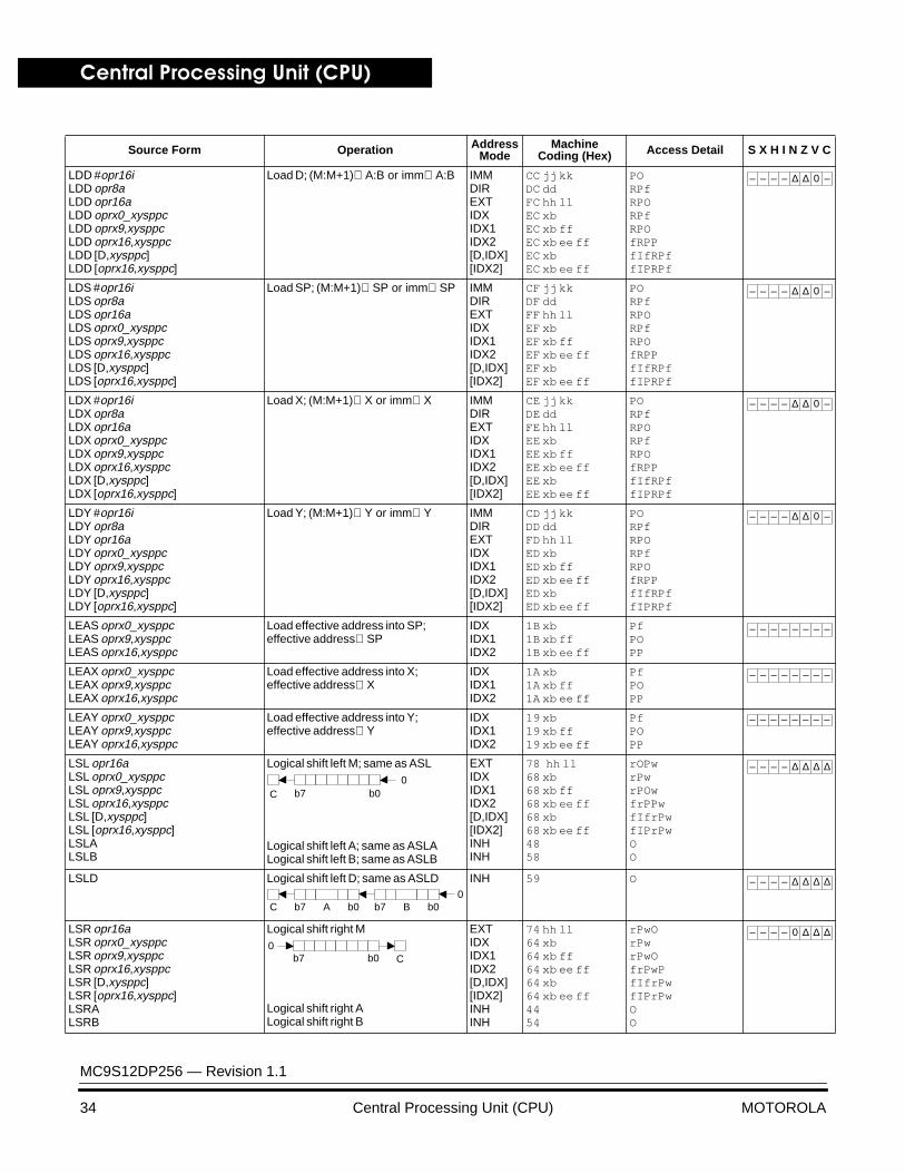
LDD #opr16iLDD opr8aLDD opr16aLDD oprx0_xysppcLDD oprx9,xysppcLDD oprx16,xysppcLDD [D,xysppc]LDD [oprx16,xysppc]
Load D; (M:M+1)⇒ A:B or imm⇒ A:B IMMDIREXTIDXIDX1IDX2[D,IDX][IDX2]
CC jj kkDC ddFC hh llEC xbEC xb ffEC xb ee ffEC xbEC xb ee ff
PORPfRPORPfRPOfRPPfIfRPffIPRPf
LDS #opr16iLDS opr8aLDS opr16aLDS oprx0_xysppcLDS oprx9,xysppcLDS oprx16,xysppcLDS [D,xysppc]LDS [oprx16,xysppc]
Load SP; (M:M+1)⇒ SP or imm⇒ SP IMMDIREXTIDXIDX1IDX2[D,IDX][IDX2]
CF jj kkDF ddFF hh llEF xbEF xb ffEF xb ee ffEF xbEF xb ee ff
PORPfRPORPfRPOfRPPfIfRPffIPRPf
LDX #opr16iLDX opr8aLDX opr16aLDX oprx0_xysppcLDX oprx9,xysppcLDX oprx16,xysppcLDX [D,xysppc]LDX [oprx16,xysppc]
Load X; (M:M+1)⇒ X or imm⇒ X IMMDIREXTIDXIDX1IDX2[D,IDX][IDX2]
CE jj kkDE ddFE hh llEE xbEE xb ffEE xb ee ffEE xbEE xb ee ff
PORPfRPORPfRPOfRPPfIfRPffIPRPf
LDY #opr16iLDY opr8aLDY opr16aLDY oprx0_xysppcLDY oprx9,xysppcLDY oprx16,xysppcLDY [D,xysppc]LDY [oprx16,xysppc]
Load Y; (M:M+1)⇒ Y or imm⇒ Y IMMDIREXTIDXIDX1IDX2[D,IDX][IDX2]
CD jj kkDD ddFD hh llED xbED xb ffED xb ee ffED xbED xb ee ff
PORPfRPORPfRPOfRPPfIfRPffIPRPf
LEAS oprx0_xysppcLEAS oprx9,xysppcLEAS oprx16,xysppc
Load effective address into SP;effective address⇒ SP
IDXIDX1IDX2
1B xb1B xb ff1B xb ee ff
PfPOPP
LEAX oprx0_xysppcLEAX oprx9,xysppcLEAX oprx16,xysppc
Load effective address into X;effective address⇒ X
IDXIDX1IDX2
1A xb1A xb ff1A xb ee ff
PfPOPP
LEAY oprx0_xysppcLEAY oprx9,xysppcLEAY oprx16,xysppc
Load effective address into Y;effective address⇒ Y
IDXIDX1IDX2
19 xb19 xb ff19 xb ee ff
PfPOPP
LSL opr16aLSL oprx0_xysppcLSL oprx9,xysppcLSL oprx16,xysppcLSL [D,xysppc]LSL [oprx16,xysppc]LSLALSLB
Logical shift left M; same as ASL
Logical shift left A; same as ASLALogical shift left B; same as ASLB
EXTIDXIDX1IDX2[D,IDX][IDX2]INHINH
78 hh ll68 xb68 xb ff68 xb ee ff68 xb68 xb ee ff4858
rOPwrPwrPOwfrPPwfIfrPwfIPrPwOO
LSLD Logical shift left D; same as ASLD INH 59 O
LSR opr16aLSR oprx0_xysppcLSR oprx9,xysppcLSR oprx16,xysppcLSR [D,xysppc]LSR [oprx16,xysppc]LSRALSRB
Logical shift right M
Logical shift right ALogical shift right B
EXTIDXIDX1IDX2[D,IDX][IDX2]INHINH
74 hh ll64 xb64 xb ff64 xb ee ff64 xb64 xb ee ff4454
rPwOrPwrPwOfrPwPfIfrPwfIPrPwOO
Source Form Operation AddressMode
Machine Coding (Hex) Access Detail S X H I N Z V C
– – – – ∆ ∆ 0 –
– – – – ∆ ∆ 0 –
– – – – ∆ ∆ 0 –
– – – – ∆ ∆ 0 –
– – – – – – – –
– – – – – – – –
– – – – – – – –
C0
b7 b0
– – – – ∆ ∆ ∆ ∆
C0
b7 b0A Bb7b0
– – – – ∆ ∆ ∆ ∆
C0
b7 b0
– – – – 0 ∆ ∆ ∆
Central Processing Unit (CPU)Instruction Set Summary
MC9S12DP256 — Revision 1.1
MOTOROLA Central Processing Unit (CPU) 35
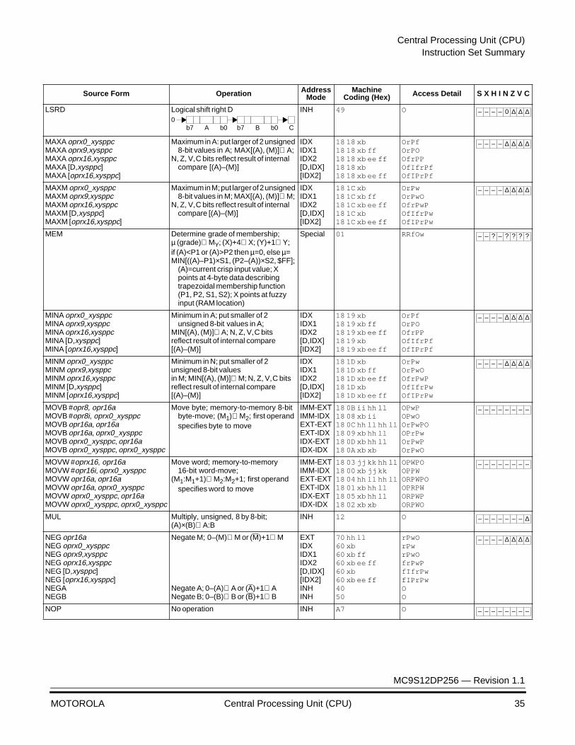
LSRD Logical shift right D INH 49 O
MAXA oprx0_xysppcMAXA oprx9,xysppcMAXA oprx16,xysppcMAXA [D,xysppc]MAXA [oprx16,xysppc]
Maximum in A: put larger of 2 unsigned 8-bit values in A; MAX[(A), (M)]⇒ A;
N, Z, V, C bits reflect result of internal compare [(A)–(M)]
IDXIDX1IDX2[D,IDX][IDX2]
18 18 xb18 18 xb ff18 18 xb ee ff18 18 xb18 18 xb ee ff
OrPfOrPOOfrPPOfIfrPfOfIPrPf
MAXM oprx0_xysppcMAXM oprx9,xysppcMAXM oprx16,xysppcMAXM [D,xysppc]MAXM [oprx16,xysppc]
Maximum in M; put larger of 2 unsigned 8-bit values in M; MAX[(A), (M)]⇒ M;
N, Z, V, C bits reflect result of internal compare [(A)–(M)]
IDXIDX1IDX2[D,IDX][IDX2]
18 1C xb18 1C xb ff18 1C xb ee ff18 1C xb18 1C xb ee ff
OrPwOrPwOOfrPwPOfIfrPwOfIPrPw
MEM Determine grade of membership;µ (grade)⇒ MY; (X)+4⇒ X; (Y)+1⇒ Y;if (A)<P1 or (A)>P2 then µ=0, else µ=MIN[((A)–P1)×S1, (P2–(A))×S2, $FF];
(A)=current crisp input value; X points at 4-byte data describing trapezoidal membership function (P1, P2, S1, S2); X points at fuzzy input (RAM location)
Special 01 RRfOw
MINA oprx0_xysppcMINA oprx9,xysppcMINA oprx16,xysppcMINA [D,xysppc]MINA [oprx16,xysppc]
Minimum in A; put smaller of 2 unsigned 8-bit values in A;
MIN[(A), (M)]⇒ A; N, Z, V, C bitsreflect result of internal compare[(A)–(M)]
IDXIDX1IDX2[D,IDX][IDX2]
18 19 xb18 19 xb ff18 19 xb ee ff18 19 xb18 19 xb ee ff
OrPfOrPOOfrPPOfIfrPfOfIPrPf
MINM oprx0_xysppcMINM oprx9,xysppcMINM oprx16,xysppcMINM [D,xysppc]MINM [oprx16,xysppc]
Minimum in N; put smaller of 2unsigned 8-bit valuesin M; MIN[(A), (M)]⇒ M; N, Z, V, C bitsreflect result of internal compare[(A)–(M)]
IDXIDX1IDX2[D,IDX][IDX2]
18 1D xb18 1D xb ff18 1D xb ee ff18 1D xb18 1D xb ee ff
OrPwOrPwOOfrPwPOfIfrPwOfIPrPw
MOVB #opr8, opr16aMOVB #opr8i, oprx0_xysppcMOVB opr16a, opr16aMOVB opr16a, oprx0_xysppcMOVB oprx0_xysppc, opr16aMOVB oprx0_xysppc, oprx0_xysppc
Move byte; memory-to-memory 8-bit byte-move; (M1)⇒ M2; first operand specifies byte to move
IMM-EXTIMM-IDXEXT-EXTEXT-IDXIDX-EXTIDX-IDX
18 0B ii hh ll18 08 xb ii18 0C hh ll hh ll18 09 xb hh ll18 0D xb hh ll18 0A xb xb
OPwPOPwOOrPwPOOPrPwOrPwPOrPwO
MOVW #oprx16, opr16aMOVW #opr16i, oprx0_xysppcMOVW opr16a, opr16aMOVW opr16a, oprx0_xysppcMOVW oprx0_xysppc, opr16aMOVW oprx0_xysppc, oprx0_xysppc
Move word; memory-to-memory 16-bit word-move;
(M1:M1+1)⇒ M2:M2+1; first operand specifies word to move
IMM-EXTIMM-IDXEXT-EXTEXT-IDXIDX-EXTIDX-IDX
18 03 jj kk hh ll18 00 xb jj kk18 04 hh ll hh ll18 01 xb hh ll18 05 xb hh ll18 02 xb xb
OPWPOOPPWORPWPOOPRPWORPWPORPWO
MUL Multiply, unsigned, 8 by 8-bit;(A)×(B)⇒ A:B
INH 12 O
NEG opr16aNEG oprx0_xysppcNEG oprx9,xysppcNEG oprx16,xysppcNEG [D,xysppc]NEG [oprx16,xysppc]NEGANEGB
Negate M; 0–(M)⇒ M or (M)+1⇒ M
Negate A; 0–(A)⇒ A or (A)+1⇒ ANegate B; 0–(B)⇒ B or (B)+1⇒ B
EXTIDXIDX1IDX2[D,IDX][IDX2]INHINH
70 hh ll60 xb60 xb ff60 xb ee ff60 xb60 xb ee ff4050
rPwOrPwrPwOfrPwPfIfrPwfIPrPwOO
NOP No operation INH A7 O
Source Form Operation AddressMode
Machine Coding (Hex) Access Detail S X H I N Z V C
Cb7 b0A Bb7b00
– – – – 0 ∆ ∆ ∆
– – – – ∆ ∆ ∆ ∆
– – – – ∆ ∆ ∆ ∆
– – ? – ? ? ? ?
– – – – ∆ ∆ ∆ ∆
– – – – ∆ ∆ ∆ ∆
– – – – – – – –
– – – – – – – –
– – – – – – – ∆
– – – – ∆ ∆ ∆ ∆
– – – – – – – –
Central Processing Unit (CPU)
MC9S12DP256 — Revision 1.1
36 Central Processing Unit (CPU) MOTOROLA
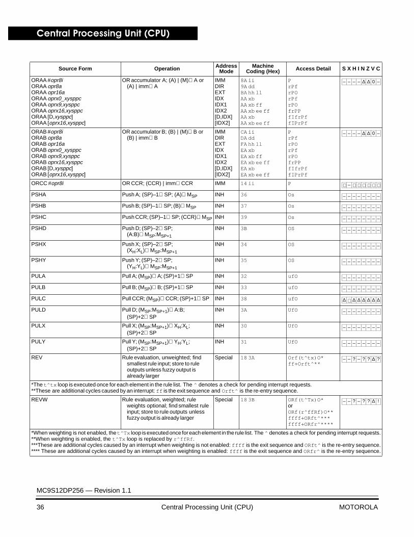
ORAA #opr8iORAA opr8aORAA opr16aORAA oprx0_xysppcORAA oprx9,xysppcORAA oprx16,xysppcORAA [D,xysppc]ORAA [oprx16,xysppc]
OR accumulator A; (A) | (M)⇒ A or (A) | imm⇒ A
IMMDIREXTIDXIDX1IDX2[D,IDX][IDX2]
8A ii9A ddBA hh llAA xbAA xb ffAA xb ee ffAA xbAA xb ee ff
PrPfrPOrPfrPOfrPPfIfrPffIPrPf
ORAB #opr8iORAB opr8aORAB opr16aORAB oprx0_xysppcORAB oprx9,xysppcORAB oprx16,xysppcORAB [D,xysppc]ORAB [oprx16,xysppc]
OR accumulator B; (B) | (M)⇒ B or (B) | imm⇒ B
IMMDIREXTIDXIDX1IDX2[D,IDX][IDX2]
CA iiDA ddFA hh llEA xbEA xb ffEA xb ee ffEA xbEA xb ee ff
PrPfrPOrPfrPOfrPPfIfrPffIPrPf
ORCC #opr8i OR CCR; (CCR) | imm⇒ CCR IMM 14 ii P
PSHA Push A; (SP)–1⇒ SP; (A)⇒ MSP INH 36 Os
PSHB Push B; (SP)–1⇒ SP; (B)⇒ MSP INH 37 Os
PSHC Push CCR; (SP)–1⇒ SP; (CCR)⇒ MSP INH 39 Os
PSHD Push D; (SP)–2⇒ SP; (A:B)⇒ MSP:MSP+1
INH 3B OS
PSHX Push X; (SP)–2⇒ SP; (XH:XL)⇒ MSP:MSP+1
INH 34 OS
PSHY Push Y; (SP)–2⇒ SP; (YH:YL)⇒ MSP:MSP+1
INH 35 OS
PULA Pull A; (MSP)⇒ A; (SP)+1⇒ SP INH 32 ufO
PULB Pull B; (MSP)⇒ B; (SP)+1⇒ SP INH 33 ufO
PULC Pull CCR; (MSP)⇒ CCR; (SP)+1⇒ SP INH 38 ufO
PULD Pull D; (MSP:MSP+1)⇒ A:B; (SP)+2⇒ SP
INH 3A UfO
PULX Pull X; (MSP:MSP+1)⇒ XH:XL; (SP)+2⇒ SP
INH 30 UfO
PULY Pull Y; (MSP:MSP+1)⇒ YH:YL; (SP)+2⇒ SP
INH 31 UfO
REV Rule evaluation, unweighted; find smallest rule input; store to rule outputs unless fuzzy output is already larger
Special 18 3A Orf(t^tx)O*ff+Orft^**
*The t^tx loop is executed once for each element in the rule list. The ^ denotes a check for pending interrupt requests.**These are additional cycles caused by an interrupt: ff is the exit sequence and Orft^ is the re-entry sequence.
REVW Rule evaluation, weighted; rule weights optional; find smallest rule input; store to rule outputs unless fuzzy output is already larger
Special 18 3B ORf(t^Tx)O*orORf(r^ffRf)O**ffff+ORft^***ffff+ORfr^****
*When weighting is not enabled, the t^Tx loop is executed once for each element in the rule list. The ̂ denotes a check for pending interrupt requests.**When weighting is enabled, the t^Tx loop is replaced by r^ffRf.***These are additional cycles caused by an interrupt when weighting is not enabled: ffff is the exit sequence and ORft^ is the re-entry sequence.**** These are additional cycles caused by an interrupt when weighting is enabled: ffff is the exit sequence and ORfr^ is the re-entry sequence.
Source Form Operation AddressMode
Machine Coding (Hex) Access Detail S X H I N Z V C
– – – – ∆ ∆ 0 –
– – – – ∆ ∆ 0 –
⇑ – ⇑ ⇑ ⇑ ⇑ ⇑ ⇑
– – – – – – – –
– – – – – – – –
– – – – – – – –
– – – – – – – –
– – – – – – – –
– – – – – – – –
– – – – – – – –
– – – – – – – –
∆ ⇓ ∆ ∆ ∆ ∆ ∆ ∆
– – – – – – – –
– – – – – – – –
– – – – – – – –
– – ? – ? ? ∆ ?
– – ? – ? ? ∆ !

Central Processing Unit (CPU)Instruction Set Summary
MC9S12DP256 — Revision 1.1
MOTOROLA Central Processing Unit (CPU) 37
ROL opr16aROL oprx0_xysppcROL oprx9,xysppcROL oprx16,xysppcROL [D,xysppc]ROL [oprx16,xysppc]ROLAROLB
Rotate left M
Rotate left ARotate left B
EXTIDXIDX1IDX2[D,IDX][IDX2]INHINH
75 hh ll65 xb65 xb ff65 xb ee ff65 xb65 xb ee ff4555
rPwOrPwrPwOfrPwPfIfrPwfIPrPwOO
ROR opr16aROR oprx0_xysppcROR oprx9,xysppcROR oprx16,xysppcROR [D,xysppc]ROR [oprx16,xysppc]RORARORB
Rotate right M
Rotate right ARotate right B
EXTIDXIDX1IDX2[D,IDX][IDX2]INHINH
76 hh ll66 xb66 xb ff66 xb ee ff66 xb66 xb ee ff4656
rPwOrPwrPwOfrPwPfIfrPwfIPrPwOO
RTC Return from call; (MSP)⇒ PPAGE;(SP)+1⇒ SP;(MSP:MSP+1)⇒ PCH:PCL;(SP)+2⇒ SP
INH 0A uUnfPPP
RTI Return from interrupt;(MSP)⇒ CCR; (SP)+1⇒ SP;(MSP:MSP+1)⇒ B:A;(SP)+2⇒ SP;(MSP:MSP+1)⇒ XH:XL;(SP)+4⇒ SP;(MSP:MSP+1)⇒ PCH:PCL;(SP)+2⇒ SP;(MSP:MSP+1)⇒ YH:YL;(SP)+4⇒ SP
INH 0B uUUUUPPPoruUUUUfVfPPP*
*RTI takes 11 cycles if an interrupt is pending.
RTS Return from subroutine;(MSP:MSP+1)⇒ PCH:PCL;(SP)+2⇒ SP
INH 3D UfPPP
SBA Subtract B from A; (A)–(B)⇒ A INH 18 16 OO
SBCA #opr8iSBCA opr8aSBCA opr16aSBCA oprx0_xysppcSBCA oprx9,xysppcSBCA oprx16,xysppcSBCA [D,xysppc]SBCA [oprx16,xysppc]
Subtract with carry from A;(A)–(M)–C⇒ A or (A)–imm–C⇒ A
IMMDIREXTIDXIDX1IDX2[D,IDX][IDX2]
82 ii92 ddB2 hh llA2 xbA2 xb ffA2 xb ee ffA2 xbA2 xb ee ff
PrPfrPOrPfrPOfrPPfIfrPffIPrPf
SBCB #opr8iSBCB opr8aSBCB opr16aSBCB oprx0_xysppcSBCB oprx9,xysppcSBCB oprx16,xysppcSBCB [D,xysppc]SBCB [oprx16,xysppc]
Subtract with carry from B;(B)–(M)–C⇒ B or (B)–imm–C⇒ B
IMMDIREXTIDXIDX1IDX2[D,IDX][IDX2]
C2 iiD2 ddF2 hh llE2 xbE2 xb ffE2 xb ee ffE2 xbE2 xb ee ff
PrPfrPOrPfrPOfrPPfIfrPffIPrPf
SEC Set C; assembles as ORCC #$01 IMM 14 01 P
SEI Set I; assembles as ORCC #$10 IMM 14 10 P
SEV Set V; assembles as ORCC #$02 IMM 14 02 P
SEX abc,dxysp Sign extend; 8-bit r1 to 16-bit r2;$00:(r1)⇒ r2 if r1 bit 7 is 0 or$FF:(r1)⇒ r2 if r1, bit 7 is 1;alternate mnemonic for TFR r1, r2
INH B7 eb P
Source Form Operation AddressMode
Machine Coding (Hex) Access Detail S X H I N Z V C
C b7 b0
– – – – ∆ ∆ ∆ ∆
Cb7b0
– – – – ∆ ∆ ∆ ∆
– – – – – – – –
∆ ⇓ ∆ ∆ ∆ ∆ ∆ ∆
– – – – – – – –
– – – – ∆ ∆ ∆ ∆
– – – – ∆ ∆ ∆ ∆
– – – – ∆ ∆ ∆ ∆
– – – – – – – 1
– – – 1 – – – –
– – – – – – 1 –
– – – – – – – –

Central Processing Unit (CPU)
MC9S12DP256 — Revision 1.1
38 Central Processing Unit (CPU) MOTOROLA
STAA opr8aSTAA opr16aSTAA oprx0_xysppcSTAA oprx9,xysppcSTAA oprx16,xysppcSTAA [D,xysppc]STAA [oprx16,xysppc]
Store accumulator A; (A)⇒ M DIREXTIDXIDX1IDX2[D,IDX][IDX2]
5A dd7A hh ll6A xb6A xb ff6A xb ee ff6A xb6A xb ee ff
PwPwOPwPwOPwPPIfwPIPw
STAB opr8aSTAB opr16aSTAB oprx0_xysppcSTAB oprx9,xysppcSTAB oprx16,xysppcSTAB [D,xysppc]STAB [oprx16,xysppc]
Store accumulator B; (B)⇒ M DIREXTIDXIDX1IDX2[D,IDX][IDX2]
5B dd7B hh ll6B xb6B xb ff6B xb ee ff6B xb6B xb ee ff
PwPwOPwPwOPwPPIfwPIPw
STD opr8aSTD opr16aSTD oprx0_xysppcSTD oprx9,xysppcSTD oprx16,xysppcSTD [D,xysppc]STD [oprx16,xysppc]
Store D; (A:B)⇒ M:M+1 DIREXTIDXIDX1IDX2[D,IDX][IDX2]
5C dd7C hh ll6C xb6C xb ff6C xb ee ff6C xb6C xb ee ff
PWPWOPWPWOPWPPIfWPIPW
STOP Stop processing; (SP)–2⇒ SP;RTNH:RTNL⇒ MSP:MSP+1;(SP)–2⇒ SP; (YH:YL)⇒ MSP:MSP+1;(SP)–2⇒ SP; (XH:XL)⇒ MSP:MSP+1;(SP)–2⇒ SP; (B:A)⇒ MSP:MSP+1;(SP)–1⇒ SP; (CCR)⇒ MSP;stop all clocks
INH 18 3E OOSSSSsf (enter stop mode)
fVfPPP (exit stop mode)
ff (continue stop mode)
OO (if stop mode disabled by S=1)
STS opr8aSTS opr16aSTS oprx0_xysppcSTS oprx9,xysppcSTS oprx16,xysppcSTS [D,xysppc]STS [oprx16,xysppc]
Store SP; (SPH:SPL)⇒ M:M+1 DIREXTIDXIDX1IDX2[D,IDX][IDX2]
5F dd7F hh ll6F xb6F xb ff6F xb ee ff6F xb6F xb ee ff
PWPWOPWPWOPWPPIfWPIPW
STX opr8aSTX opr16aSTX oprx0_xysppcSTX oprx9,xysppcSTX oprx16,xysppcSTX [D,xysppc]STX [oprx16,xysppc]
Store X; (XH:XL)⇒ M:M+1 DIREXTIDXIDX1IDX2[D,IDX][IDX2]
5E dd7E hh ll6E xb6E xb ff6E xb ee ff6E xb6E xb ee ff
PWPWOPWPWOPWPPIfWPIPW
STY opr8aSTY opr16aSTY oprx0_xysppcSTY oprx9,xysppcSTY oprx16,xysppcSTY [D,xysppc]STY [oprx16,xysppc]
Store Y; (YH:YL)⇒ M:M+1 DIREXTIDXIDX1IDX2[D,IDX][IDX2]
5D dd7D hh ll6D xb6D xb ff6D xb ee ff6D xb6D xb ee ff
PWPWOPWPWOPWPPIfWPIPW
SUBA #opr8iSUBA opr8aSUBA opr16aSUBA oprx0_xysppcSUBA oprx9,xysppcSUBA oprx16,xysppcSUBA [D,xysppc]SUBA [oprx16,xysppc]
Subtract from A; (A)–(M)⇒ A or (A)–imm⇒ A
IMMDIREXTIDXIDX1IDX2[D,IDX][IDX2]
80 ii90 ddB0 hh llA0 xbA0 xb ffA0 xb ee ffA0 xbA0 xb ee ff
PrPfrPOrPfrPOfrPPfIfrPffIPrPf
Source Form Operation AddressMode
Machine Coding (Hex) Access Detail S X H I N Z V C
– – – – ∆ ∆ 0 –
– – – – ∆ ∆ 0 –
– – – – ∆ ∆ 0 –
– – – – – – – –
– – – – ∆ ∆ 0 –
– – – – ∆ ∆ 0 –
– – – – ∆ ∆ 0 –
– – – – ∆ ∆ ∆ ∆
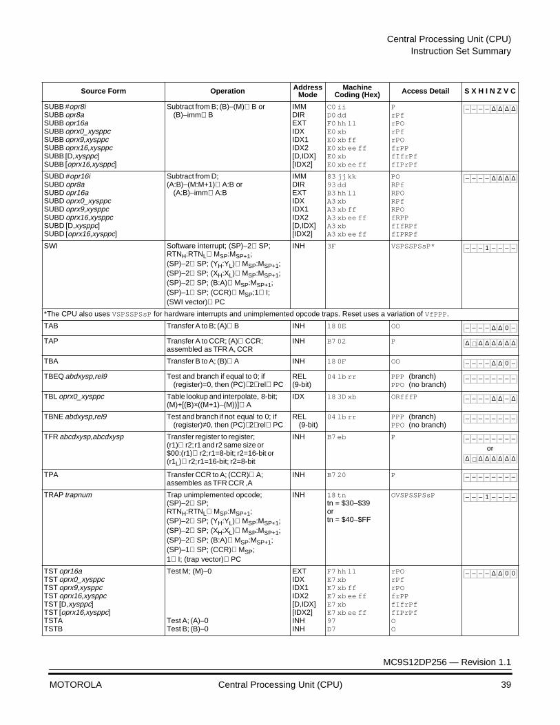
Central Processing Unit (CPU)Instruction Set Summary
MC9S12DP256 — Revision 1.1
MOTOROLA Central Processing Unit (CPU) 39
SUBB #opr8iSUBB opr8aSUBB opr16aSUBB oprx0_xysppcSUBB oprx9,xysppcSUBB oprx16,xysppcSUBB [D,xysppc]SUBB [oprx16,xysppc]
Subtract from B; (B)–(M)⇒ B or (B)–imm⇒ B
IMMDIREXTIDXIDX1IDX2[D,IDX][IDX2]
C0 iiD0 ddF0 hh llE0 xbE0 xb ffE0 xb ee ffE0 xbE0 xb ee ff
PrPfrPOrPfrPOfrPPfIfrPffIPrPf
SUBD #opr16iSUBD opr8aSUBD opr16aSUBD oprx0_xysppcSUBD oprx9,xysppcSUBD oprx16,xysppcSUBD [D,xysppc]SUBD [oprx16,xysppc]
Subtract from D;(A:B)–(M:M+1)⇒ A:B or
(A:B)–imm⇒ A:B
IMMDIREXTIDXIDX1IDX2[D,IDX][IDX2]
83 jj kk93 ddB3 hh llA3 xbA3 xb ffA3 xb ee ffA3 xbA3 xb ee ff
PORPfRPORPfRPOfRPPfIfRPffIPRPf
SWI Software interrupt; (SP)–2⇒ SP;RTNH:RTNL⇒ MSP:MSP+1;(SP)–2⇒ SP; (YH:YL)⇒ MSP:MSP+1;(SP)–2⇒ SP; (XH:XL)⇒ MSP:MSP+1;(SP)–2⇒ SP; (B:A)⇒ MSP:MSP+1;(SP)–1⇒ SP; (CCR)⇒ MSP;1⇒ I;(SWI vector)⇒ PC
INH 3F VSPSSPSsP*
*The CPU also uses VSPSSPSsP for hardware interrupts and unimplemented opcode traps. Reset uses a variation of VfPPP.
TAB Transfer A to B; (A)⇒ B INH 18 0E OO
TAP Transfer A to CCR; (A)⇒ CCR;assembled as TFR A, CCR
INH B7 02 P
TBA Transfer B to A; (B)⇒ A INH 18 0F OO
TBEQ abdxysp,rel9 Test and branch if equal to 0; if (register)=0, then (PC)+2+rel⇒ PC
REL(9-bit)
04 lb rr PPP (branch)PPO (no branch)
TBL oprx0_xysppc Table lookup and interpolate, 8-bit;(M)+[(B)×((M+1)–(M))]⇒ A
IDX 18 3D xb ORfffP
TBNE abdxysp,rel9 Test and branch if not equal to 0; if (register)≠0, then (PC)+2+rel⇒ PC
REL(9-bit)
04 lb rr PPP (branch)PPO (no branch)
TFR abcdxysp,abcdxysp Transfer register to register;(r1)⇒ r2; r1 and r2 same size or$00:(r1)⇒ r2; r1=8-bit; r2=16-bit or(r1L)⇒ r2; r1=16-bit; r2=8-bit
INH B7 eb P
or
TPA Transfer CCR to A; (CCR)⇒ A;assembles as TFR CCR ,A
INH B7 20 P
TRAP trapnum Trap unimplemented opcode;(SP)–2⇒ SP;RTNH:RTNL⇒ MSP:MSP+1;(SP)–2⇒ SP; (YH:YL)⇒ MSP:MSP+1;(SP)–2⇒ SP; (XH:XL)⇒ MSP:MSP+1;(SP)–2⇒ SP; (B:A)⇒ MSP:MSP+1;(SP)–1⇒ SP; (CCR)⇒ MSP;1⇒ I; (trap vector)⇒ PC
INH 18 tntn = $30–$39ortn = $40–$FF
OVSPSSPSsP
TST opr16aTST oprx0_xysppcTST oprx9,xysppcTST oprx16,xysppcTST [D,xysppc]TST [oprx16,xysppc]TSTATSTB
Test M; (M)–0
Test A; (A)–0Test B; (B)–0
EXTIDXIDX1IDX2[D,IDX][IDX2]INHINH
F7 hh llE7 xbE7 xb ffE7 xb ee ffE7 xbE7 xb ee ff97D7
rPOrPfrPOfrPPfIfrPffIPrPfOO
Source Form Operation AddressMode
Machine Coding (Hex) Access Detail S X H I N Z V C
– – – – ∆ ∆ ∆ ∆
– – – – ∆ ∆ ∆ ∆
– – – 1 – – – –
– – – – ∆ ∆ 0 –
∆ ⇓ ∆ ∆ ∆ ∆ ∆ ∆
– – – – ∆ ∆ 0 –
– – – – – – – –
– – – – ∆ ∆ – ∆
– – – – – – – –
– – – – – – – –
∆ ⇓ ∆ ∆ ∆ ∆ ∆ ∆
– – – – – – – –
– – – 1 – – – –
– – – – ∆ ∆ 0 0
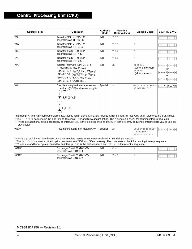
Central Processing Unit (CPU)
MC9S12DP256 — Revision 1.1
40 Central Processing Unit (CPU) MOTOROLA
TSX Transfer SP to X; (SP)⇒ X;assembles as TFR SP,X
INH B7 75 P
TSY Transfer SP to Y; (SP)⇒ Y;assembles as TFR SP,Y
INH B7 76 P
TXS Transfer X to SP; (X)⇒ SP;assembles as TFR X,SP
INH B7 57 P
TYS Transfer Y to SP; (Y)⇒ SP;assembles as TFR Y,SP
INH B7 67 P
WAI Wait for interrupt; (SP)–2⇒ SP;RTNH:RTNL⇒ MSP:MSP+1;(SP)–2⇒ SP; (YH:YL)⇒ MSP:MSP+1;(SP)–2⇒ SP; (XH:XL)⇒ MSP:MSP+1;(SP)–2⇒ SP; (B:A)⇒ MSP:MSP+1;(SP)–1⇒ SP; (CCR)⇒ MSP
INH 3E OSSSSsf (before interrupt)fVfPPP (after interrupt)
or
or
WAV Calculate weighted average; sum of products (SOP) and sum of weights (SOW)*
Special 18 3C Of(frr^ffff)O**SSS+UUUrr^***
*Initialize B, X, and Y: B= number of elements; X points at first element in Si list; Y points at first element in Fi list. All Si and Fi elements are 8-bit values.**The frr^ffff sequence is the loop for one iteration of SOP and SOW accumulation. The ^ denotes a check for pending interrupt requests.***These are additional cycles caused by an interrupt: SSS is the exit sequence and UUUrr^ is the re-entry sequence. Intermediate values use six
stack bytes.
wavr* Resume executing interrupted WAV Special 3C UUUrr^ffff(frr^ffff)O**
SSS+UUUrr^***
*wavr is a pseudoinstruction that recovers intermediate results from the stack rather than initializing them to 0.**The frr^ffff sequence is the loop for one iteration of SOP and SOW recovery. The ^ denotes a check for pending interrupt requests.***These are additional cycles caused by an interrupt: SSS is the exit sequence and UUUrr^ is the re-entry sequence.
XGDX Exchange D with X; (D)⇔(X);assembles as EXG D, X
INH B7 C5 P
XGDY Exchange D with Y; (D)⇔(Y);assembles as EXG D, Y
INH B7 C6 P
Source Form Operation AddressMode
Machine Coding (Hex) Access Detail S X H I N Z V C
– – – – – – – –
– – – – – – – –
– – – – – – – –
– – – – – – – –
– – – – – – – –
– – – 1 – – – –
– 1 – 1 – – – –
Fii 1=
B
∑ X⇒
SiFii 1=
B
∑ Y:D⇒
– – ? – ? ∆ ? ?
– – ? – ? ∆ ? ?
– – – – – – – –
– – – – – – – –

MC9S12DP256 — Revision 1.1
MOTOROLA Pinout and Signal Description 41
Pinout and Signal DescriptionPinout and Signal Description
Contents
MC9S12DP256 Pin Assignments in 112-pin QFP . . . . . . . . . . . . . . . 41Power Supply Pins . . . . . . . . . . . . . . . . . . . . . . . . . . . . . . . . . . . . . . . 44Signal Descriptions . . . . . . . . . . . . . . . . . . . . . . . . . . . . . . . . . . . . . . . 47Port Signals. . . . . . . . . . . . . . . . . . . . . . . . . . . . . . . . . . . . . . . . . . . . . 58
MC9S12DP256 Pin Assignments in 112-pin QFP
The MC9S12DP256 is available in a 112-pin low profile quad flat pack (LQFP). Most pins perform two or more functions, as described in the Signal Descriptions. Figure 3 shows pin assignments. In expanded narrow modes the lower byte data is multiplexed with higher byte data through pins PTA7:0.
NOTE: The main body of this document refers to the 112-pin version of the device. Pins shown in bold on the block diagram and pinout are not available on the 80-pin version. Contact your Motorola representative for further information on the 80-pin option.
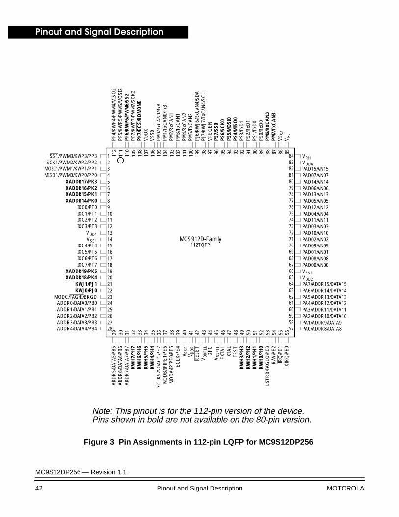
Pinout and Signal Description
MC9S12DP256 — Revision 1.1
42 Pinout and Signal Description MOTOROLA
Figure 3 Pin Assignments in 112-pin LQFP for MC9S12DP256
VRHVDDAPAD15/AN15PAD07/AN07PAD14/AN14PAD06/AN06PAD13/AN13PAD05/AN05PAD12/AN12PAD04/AN04PAD11/AN11PAD03/AN03PAD10/AN10PAD02/AN02PAD09/AN09PAD01/AN01PAD08/AN08PAD00/AN00VSS2VDD2PA7/ADDR15/DATA15PA6/ADDR14/DATA14PA5/ADDR13/DATA13PA4/ADDR12/DATA12PA3/ADDR11/DATA11PA2/ADDR10/DATA10PA1/ADDR9/DATA9PA0/ADDR8/DATA8
PP4/
KWP4
/PW
M4/
MIS
O2
PP5/
KWP5
/PW
M5/
MO
SI2
PP6/
KW
P6/P
WM
6/SS
2PP
7/KW
P7/P
WM
7/SC
K2PK
7/EC
S/RO
MO
NE
VD
DX
VS
SX
PM0/
RxC
AN0/
RxB
PM1/
TxC
AN0/
TxB
PM2/
RxC
AN1
PM3/
TxC
AN1
PM4/
RxC
AN2
PM5/
TxC
AN2
PJ6/
KWJ6
/RxC
AN4/
SDA
PJ7/
KWJ7
/TxC
AN4/
SCL
VR
EG
EN
PS7/
SS0
PS6/
SCK
0PS
5/M
OSI
0PS
4/M
ISO
0PS
3/Tx
D1
PS2/
RxD
1PS
1/Tx
D0
PS0/
RxD
0PM
6/R
xCA
N3
PM7/
TxC
AN
3V
SS
AV
RL
SS1/PWM3/KWP3/PP3SCK1/PWM2/KWP2/PP2
MOSI1/PWM1/KWP1/PP1MISO1/PWM0/KWP0/PP0
XADDR17/PK3XADDR16/PK2XADDR15/PK1XADDR14/PK0
IOC0/PT0IOC1/PT1IOC2/PT2IOC3/PT3
VDD1VSS1
IOC4/PT4IOC5/PT5IOC6/PT6IOC7/PT7
XADDR19/PK5XADDR18/PK4
KWJ1/PJ1KWJ0/PJ0
MODC/TAGHI/BKGDADDR0/DATA0/PB0ADDR1/DATA1/PB1ADDR2/DATA2/PB2ADDR3/DATA3/PB3ADDR4/DATA4/PB4
ADD
R5/
DAT
A5/P
B5AD
DR
6/D
ATA6
/PB6
ADD
R7/
DAT
A7/P
B7K
WH
7/PH
7K
WH
6/PH
6K
WH
5/PH
5K
WH
4/PH
4X
CLK
S/N
OAC
C/P
E7M
OD
B/IP
IPE1
/PE6
MO
DA/
IPIP
E0/P
E5EC
LK/P
E4V
SS
RV
DD
RR
ES
ET
VD
DP
LLX
FCV
SS
PLL
EX
TAL
XTAL
TES
TK
WH
3/PH
3K
WH
2/PH
2K
WH
1/PH
1K
WH
0/PH
0LS
TRB
/TAG
LO/P
E3R
/W/P
E2IR
Q/P
E1XI
RQ
/PE0
MCS912D-Family112TQFP
112
111
110
109
108
107
106
105
104
103
102
101
100 99 98 97 96 95 94 93 92 91 90 89 88 87 86 85
12345678910111213141516171819202122232425262728
29 30 31 32 33 34 35 36 37 38 39 40 41 42 43 44 45 46 47 48 49 50 51 52 53 54 55 56
84838281807978777675747372717069686766656463626160595857
Note: This pinout is for the 112-pin version of the device.Pins shown in bold are not available on the 80-pin version.

Pinout and Signal DescriptionMC9S12DP256 Pin Assignments in 112-pin QFP
MC9S12DP256 — Revision 1.1
MOTOROLA Pinout and Signal Description 43
Figure 4 112-pin QFP Mechanical Dimensions (case no. 987)
DIMA
MIN MAX20.000 BSC
MILLIMETERS
A1 10.000 BSCB 20.000 BSC
B1 10.000 BSCC --- 1.600
C1 0.050 0.150C2 1.350 1.450D 0.270 0.370E 0.450 0.750F 0.270 0.330G 0.650 BSCJ 0.090 0.170K 0.500 REFP 0.325 BSC
R1 0.100 0.200R2 0.100 0.200S 22.000 BSC
S1 11.000 BSCV 22.000 BSC
V1 11.000 BSCY 0.250 REFZ 1.000 REF
AA 0.090 0.160θ
θθθ 11 °
11 °13 °
7 °
13 °
VIEW Y
L-M0.20 NT4X 4X 28 TIPS
PIN 1IDENT
1
112 85
84
28 57
29 56
B V
V1B1
A1
S1
A
S
VIEW AB
0.10
3
CC2
θ
2θ0.050
SEATINGPLANE
GAGE PLANE
1θ
θ
VIEW AB
C1
(Z)
(Y)E
(K)
R2
R1 0.25
J1
VIEW Y
J1
P
G108X
4X
SECTION J1-J1
BASE
ROTATED 90 COUNTERCLOCKWISE°
METAL
J AA
FD
L-MM0.13 NT
123
CL
L-M0.20 NT
L
N
M
T
T
112X
XX=L, M OR N
R
R
NOTES:1. DIMENSIONING AND TOLERANCING PER
ASME Y14.5M, 1994.2. DIMENSIONS IN MILLIMETERS.3. DATUMS L, M AND N TO BE DETERMINED AT
SEATING PLANE, DATUM T.4. DIMENSIONS S AND V TO BE DETERMINED AT
SEATING PLANE, DATUM T.5. DIMENSIONS A AND B DO NOT INCLUDE
MOLD PROTRUSION. ALLOWABLE PROTRUSION IS 0.25 PER SIDE. DIMENSIONS A AND B INCLUDE MOLD MISMATCH.
6. DIMENSION D DOES NOT INCLUDE DAMBARPROTRUSION. ALLOWABLE DAMBARPROTRUSION SHALL NOT CAUSE THE D DIMENSION TO EXCEED 0.46.
8 ° 3 ° 0 °
Pinout and Signal Description
MC9S12DP256 — Revision 1.1
44 Pinout and Signal Description MOTOROLA
Power Supply Pins
MC9S12DP256 power and ground pins are described below and summarized in Table 6.
External Power (VDDX) and Ground (VSSX)
External power and ground for I/O drivers. Because fast signal transitions place high, short-duration current demands on the power supply, use bypass capacitors with high-frequency characteristics and place them as close to the MCU as possible. Bypass requirements depend on how heavily the MCU pins are loaded.
External Power (VDDR) and Ground (VSSR)
External power and ground for I/O drivers and input to the internal voltage regulator. Because fast signal transitions place high, short-duration current demands on the power supply, use bypass capacitors with high-frequency characteristics and place them as close to the MCU as possible. Bypass requirements depend on how heavily the MCU pins are loaded.
Internal Power (VDD1,2) and Ground (VSS1,2)
Power is supplied to the MCU through VDD and VSS. Because fast signal transitions place high, short-duration current demands on the power supply, use bypass capacitors with high-frequency characteristics and place them as close to the MCU as possible. This 2.5V supply is derived from the internal voltage regulator. There is no static load on those pins allowed. The internal voltage regulator is turned off, if VREGEN is tied to ground.
VDDA, VSSA Provides operating voltage and ground for the analog-to-digital converters. It provides also the reference for the internal voltage regulator.This allows the supply voltage to the A/D and the reference voltage to be bypassed independently.
Analog to Digital Reference Voltages (VRH, VRL)
Provides reference voltage and ground for the analog-to-digital converters.
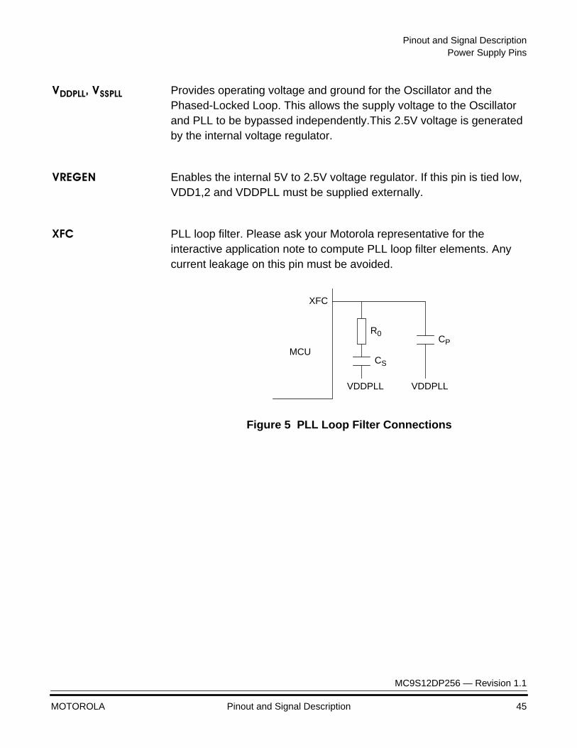
Pinout and Signal DescriptionPower Supply Pins
MC9S12DP256 — Revision 1.1
MOTOROLA Pinout and Signal Description 45
VDDPLL, VSSPLL Provides operating voltage and ground for the Oscillator and the Phased-Locked Loop. This allows the supply voltage to the Oscillator and PLL to be bypassed independently.This 2.5V voltage is generated by the internal voltage regulator.
VREGEN Enables the internal 5V to 2.5V voltage regulator. If this pin is tied low, VDD1,2 and VDDPLL must be supplied externally.
XFC PLL loop filter. Please ask your Motorola representative for the interactive application note to compute PLL loop filter elements. Any current leakage on this pin must be avoided.
Figure 5 PLL Loop Filter Connections
MCU
XFC
R0
CS
CP
VDDPLLVDDPLL

Pinout and Signal Description
MC9S12DP256 — Revision 1.1
46 Pinout and Signal Description MOTOROLA
Table 6 MC9S12DP256 Power and Ground Connection Summary
MnemonicPin Number Nominal
Voltage Description112-pin QFP
VDD1, 2 13, 65 2.5 VInternal power and ground generated by internal regulator
VSS1, 2 14, 66 0V
VDDR 41 5.0 V External power and ground, supply to pin drivers and internal voltage regulator.VSSR 40 0 V
VDDX 107 5.0 VExternal power and ground, supply to pin drivers.
VSSX 106 0 V
VDDA 83 5.0 V Operating voltage and ground for the analog-to-digital converters and the reference for the internal voltage regulator, allows the supply voltage to the A/D to be bypassed independently.
VSSA 86 0 V
VRL 85 0 VReference voltages for the analog-to-digital converter.
VRH 84 5.0 V
VDDPLL 43 2.5 V Provides operating voltage and ground for the Phased-Locked Loop. This allows the supply voltage to the PLL to be bypassed independently. Internal power and ground generated by internal regulator.
VSSPLL 45 0 V
VREGEN 97 5V Internal Voltage Regulator enable/disable
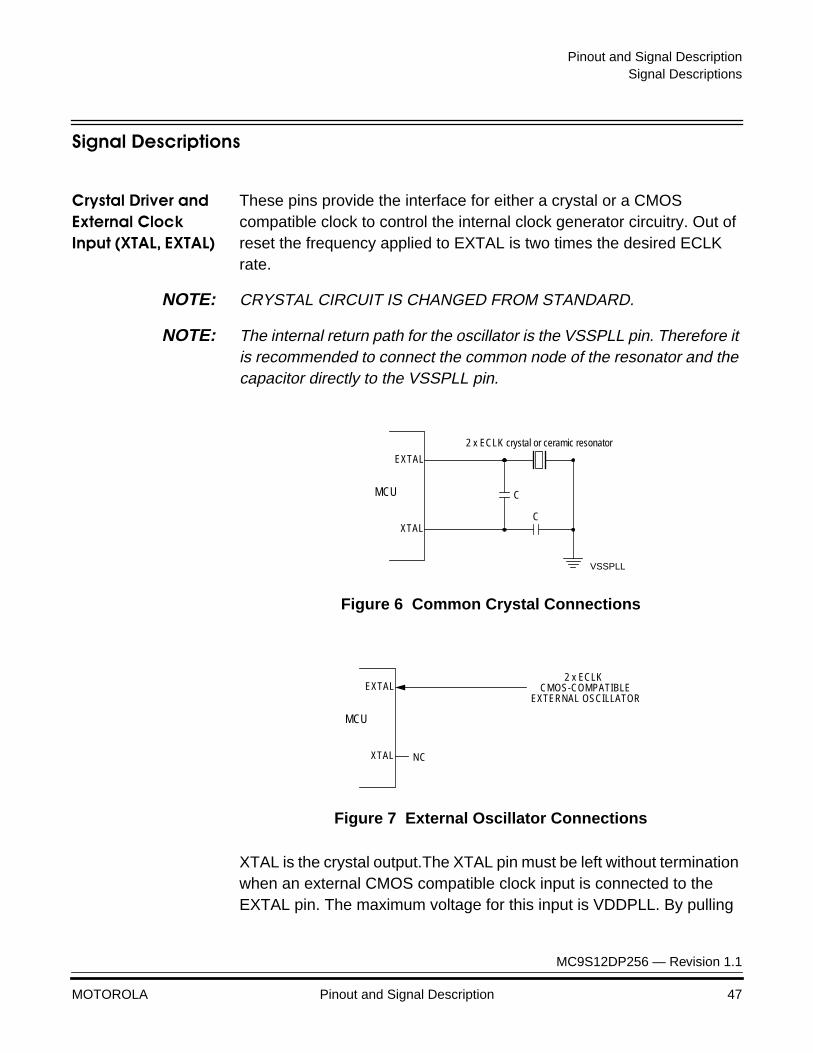
Pinout and Signal DescriptionSignal Descriptions
MC9S12DP256 — Revision 1.1
MOTOROLA Pinout and Signal Description 47
Signal Descriptions
Crystal Driver and External Clock Input (XTAL, EXTAL)
These pins provide the interface for either a crystal or a CMOS compatible clock to control the internal clock generator circuitry. Out of reset the frequency applied to EXTAL is two times the desired ECLK rate.
NOTE: CRYSTAL CIRCUIT IS CHANGED FROM STANDARD.
NOTE: The internal return path for the oscillator is the VSSPLL pin. Therefore it is recommended to connect the common node of the resonator and the capacitor directly to the VSSPLL pin.
Figure 6 Common Crystal Connections
Figure 7 External Oscillator Connections
XTAL is the crystal output.The XTAL pin must be left without termination when an external CMOS compatible clock input is connected to the EXTAL pin. The maximum voltage for this input is VDDPLL. By pulling
CMCU
C
EXTAL
XTAL
2 x ECLK crystal or ceramic resonator
VSSPLL
NC
MCU
EXTAL
XTAL
2 x ECLKCMOS-COMPATIBLE
EXTERNAL OSCILLATOR
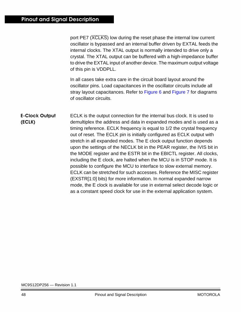
Pinout and Signal Description
MC9S12DP256 — Revision 1.1
48 Pinout and Signal Description MOTOROLA
port PE7 (XCLKS) low during the reset phase the internal low current oscillator is bypassed and an internal buffer driven by EXTAL feeds the internal clocks. The XTAL output is normally intended to drive only a crystal. The XTAL output can be buffered with a high-impedance buffer to drive the EXTAL input of another device. The maximum output voltage of this pin is VDDPLL.
In all cases take extra care in the circuit board layout around the oscillator pins. Load capacitances in the oscillator circuits include all stray layout capacitances. Refer to Figure 6 and Figure 7 for diagrams of oscillator circuits.
E-Clock Output (ECLK)
ECLK is the output connection for the internal bus clock. It is used to demultiplex the address and data in expanded modes and is used as a timing reference. ECLK frequency is equal to 1/2 the crystal frequency out of reset. The ECLK pin is initially configured as ECLK output with stretch in all expanded modes. The E clock output function depends upon the settings of the NECLK bit in the PEAR register, the IVIS bit in the MODE register and the ESTR bit in the EBICTL register. All clocks, including the E clock, are halted when the MCU is in STOP mode. It is possible to configure the MCU to interface to slow external memory. ECLK can be stretched for such accesses. Reference the MISC register (EXSTR[1:0] bits) for more information. In normal expanded narrow mode, the E clock is available for use in external select decode logic or as a constant speed clock for use in the external application system.
Pinout and Signal DescriptionSignal Descriptions
MC9S12DP256 — Revision 1.1
MOTOROLA Pinout and Signal Description 49
Reset (RESET) RESET is an active low bidirectional control signal that acts as an input to initialize the MCU to a known start-up state. It also acts as an open-drain output to indicate that an internal failure has been detected in either the clock monitor or COP watchdog circuit. The MCU goes into reset asynchronously and comes out of reset synchronously. This allows the part to reach a proper reset state even if the clocks have failed, while allowing synchronized operation when starting out of reset.
It is important to use an external low-voltage reset circuit (similar to MC33464-48) to prevent corruption of RAM or EEPROM due to power transitions.
The reset sequence is initiated by any of the following events:
• Clock monitor enabled and clock monitor detects slow or stopped clock
• COP watchdog enabled and watchdog timer times out
• Power-on Reset (POR)
• User applies a low level to the RESET pin
External circuitry connected to the RESET pin should not include a large capacitance that would interfere with the ability of this signal to rise to a valid logic one within 32 ECLK cycles after the low drive is released. Upon detection of any reset, an internal circuit drives the RESET pin low and a clocked reset sequence controls when the MCU can begin normal processing.
NOTE: Entry into reset is asynchronous and does not require a clock. However, the MCU cannot sequence out of reset without a system clock.
In the case of POR or a clock monitor failure a 4096 ECLK cycle oscillator startup delay is imposed before the reset recovery sequence starts (RESET is driven low throughout this 4096 cycle delay.) The internal reset recovery sequence then drives RESET low for 64 to 65 ECLK cycles and releases the drive to allow RESET to rise. 32 ECLK cycles later this circuit samples the RESET pin to see if it has risen to a logic one level. If RESET is low at this point, the reset is assumed to be coming from an external request and the internally latched states of the COP timeout and clock monitor failure are cleared so the normal reset
Pinout and Signal Description
MC9S12DP256 — Revision 1.1
50 Pinout and Signal Description MOTOROLA
vector ($FFFE:FFFF) is taken when RESET is finally released. If RESET is high after this 32 cycle delay, the reset source is tentatively assumed to be either a COP failure or a clock monitor failure. If the internally latched state of the clock monitor fail circuit is true, processing begins by fetching the clock monitor vector ($FFFC:FFFD). If no clock monitor failure is indicated, and the latched state of the COP timeout is true, processing begins by fetching the COP vector ($FFFA:FFFB). If neither clock monitor fail nor COP timeout are pending, processing begins by fetching the normal reset vector ($FFFE:FFFF).
Maskable Interrupt Request (IRQ)
The IRQ input provides a means of applying asynchronous interrupt requests to the MCU. Either falling edge-sensitive triggering or level-sensitive triggering is program selectable (INTCR register). IRQ is always enabled and configured to level-sensitive triggering out of reset. It can be disabled by clearing IRQEN bit (INTCR register). When the MCU is reset the IRQ function is masked in the condition code register. This pin is always an input and can always be read. There is an active pull-up on this pin while in reset and immediately out of reset. The pullup can be turned off by clearing PUPEE in the PUCR register.
Nonmaskable Interrupt (XIRQ)
The XIRQ input provides a means of requesting a nonmaskable interrupt after reset initialization. During reset, the X bit in the condition code register (CCR) is set and any interrupt is masked until MCU software enables it. Because the XIRQ input is level sensitive, it can be connected to a multiple-source wired-OR network. This pin is always an input and can always be read. There is an active pull-up on this pin while in reset and immediately out of reset. The pullup can be turned off by clearing PUPEE in the PUCR register. XIRQ is often used as a power loss detect interrupt.
Whenever XIRQ or IRQ are used with multiple interrupt sources, (IRQ must be configured for level-sensitive operation if there is more than one source of IRQ interrupt), each source must drive the interrupt input with an open-drain type of driver to avoid contention between outputs. There must also be an interlock mechanism at each interrupt source so that the source holds the interrupt line low until the MCU recognizes and acknowledges the interrupt request. If the interrupt line is held low, the
Pinout and Signal DescriptionSignal Descriptions
MC9S12DP256 — Revision 1.1
MOTOROLA Pinout and Signal Description 51
MCU will recognize another interrupt as soon as the interrupt mask bit in the MCU is cleared (normally upon return from an interrupt).
Mode Select (MODA, MODB, and MODC)
The state of these pins during reset determine the MCU operating mode. After reset, MODA and MODB can be configured as instruction queue tracking signals IPIPE0 and IPIPE1 in expanded modes. MODA, and MODB have active pulldowns during reset. MODC has the pull-up on the pin enabled after reset.
Single-Wire Background Mode Pin (BKGD) shared with MODC
The BKGD pin receives and transmits serial background debugging commands. A special self-timing protocol is used.Out of reset the pin is configured as input with internal pull-up enabled.
NOTE: The resistance of the internal pull-up may be too high depending on the speed and the load to ensure proper BDM communication. In this case an additional external pull-up resistor must be provided.
External Address and Data Buses (ADDR[15:0] and DATA[15:0])
External bus pins share functions with general-purpose I/O ports A and B. In single-chip operating modes, the pins can be used for general-purpose I/O; in expanded modes, the pins are used for the external buses.
In expanded wide mode, ports A and B are used for multiplexed 16-bit data and address buses. PA[7:0] correspond to ADDR[15:8]/DATA[15:8]; PB[7:0] correspond to ADDR[7:0]/DATA[7:0].
In expanded narrow mode, ports A and B are used for the16-bit address bus, and an 8-bit data bus is multiplexed with the most significant half of the address bus on port A. In this mode, 16-bit data is handled as two back-to-back bus cycles, one for the high byte followed by one for the low byte. PA[7:0] correspond to ADDR[15:8] and to DATA[15:8] or DATA[7:0], depending on the bus cycle. The state of the address pins should be latched at the rising edge of E. To allow for maximum address setup time at external devices, a transparent latch should be used.
Pinout and Signal Description
MC9S12DP256 — Revision 1.1
52 Pinout and Signal Description MOTOROLA
Read/Write (R/W) In all modes this pin can be used as a general-purpose I/O and is an input with an active pull-up out of reset. If the read/write function is required it should be enabled by setting the RDWE bit in the PEAR register. External writes will not be possible until enabled.
Low-Byte Strobe (LSTRB)
In all modes this pin can be used as a general-purpose I/O and is an input with an active pull-up out of reset. If the strobe function is required, it should be enabled by setting the LSTRE bit in the PEAR register. This signal is used in write operations. Therefore external low byte writes will not be possible until this function is enabled. This pin is also used as TAGLO in Special Expanded modes and is multiplexed with the LSTRB function.
Instruction Queue Tracking Signals (IPIPE1 and IPIPE0)
IPIPE1 (PE6) and IPIPE0 (PE5) signals are used to track the state of the internal instruction pipe. Data movement and execution state information is time-multiplexed on the two signals.
No Access (NOACC)
The NOACC signal (available on PE[7]) is used to indicate that the current bus cycle is an unused or “free” cycle. This signal will assert anytime that the CPU is not using the bus.
NOTE: Table 7 refers to the 112-pin version of the device. Pins shown in bold are not available on the 80-pin version. Contact your Motorola representative for further information on the 80-pin option.
Table 7 MC9S12DP256 Signal Description Summary
Pin Function Pin Name Poweredby
Pin Number Description112-pin
SS1_PWM3_KWP3 PP3 VDDX 1Pulse Width Modulator ChannelShared with input interrupts and SPI1See also pins 109–112
SCK1_PWM2_KWP2 PP2 VDDX 2
MOSI1_PWM1_KWP1 PP1 VDDX 3
MISO1_PWM0_KWP0 PP0 VDDX 4
Pinout and Signal DescriptionSignal Descriptions
MC9S12DP256 — Revision 1.1
MOTOROLA Pinout and Signal Description 53
XADDR17 PK3 VDDX 5
Expanded addressesXADDR16 PK2 VDDX 6
XADDR15 PK1 VDDX 7
XADDR14 PK0 VDDX 8
IOC0 PT0 VDDX 9
Capture Timer ChannelIOC1 PT1 VDDX 10
IOC2 PT2 VDDX 11
IOC3 PT3 VDDX 12
VDD1 VDD1 132.5V core supply
VSS1 VSS1 14
IOC4 PT4 VDDX 15
Capture Timer ChannelIOC5 PT5 VDDX 16
IOC6 PT6 VDDX 17
IOC7 PT7 VDDX 18
XADDR19 PK5 VDDX 19Expanded Addresses
XADDR18 PK4 VDDX 20
KWJ1 PJ1 VDDX 21General Purpose I/O and Interrupt
KWJ0 PJ0 VDDX 22
MODC_TAGHI BKGD VDDR 23
Pseudo_open_drain communication pin for the single-wire background debug mode. At the rising edge on RESET, the state of this pin is latched into the MODC bit to set the mode. When instruction tagging is on, a 0 at the falling edge of E tags the high half of the instruction word being read into the instruction queue.
ADDR0_DATA0 PB0 VDDR 24
External bus pins share function with general-purpose I/O port B. In single chip modes, the pins can be used for general-purpose I/O. In expanded modes, the pins are used for the external address and data buses.
ADDR1_DATA1 PB1 VDDR 25
ADDR2_DATA2 PB2 VDDR 26
ADDR3_DATA3 PB3 VDDR 27
ADDR4_DATA4 PB4 VDDR 28
ADDR5_DATA5 PB5 VDDR 29
ADDR6_DATA6 PB6 VDDR 30
ADDR7_DATA7 PB7 VDDR 31
Table 7 MC9S12DP256 Signal Description Summary
Pin Function Pin Name Poweredby
Pin Number Description112-pin
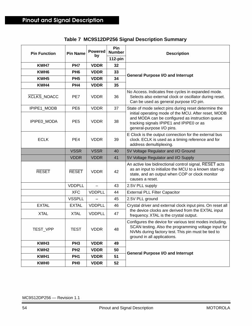
Pinout and Signal Description
MC9S12DP256 — Revision 1.1
54 Pinout and Signal Description MOTOROLA
KWH7 PH7 VDDR 32
General Purpose I/O and InterruptKWH6 PH6 VDDR 33
KWH5 PH5 VDDR 34
KWH4 PH4 VDDR 35
XCLKS_NOACC PE7 VDDR 36No Access. Indicates free cycles in expanded mode.
Selects also external clock or oscillator during reset. Can be used as general purpose I/O pin.
IPIPE1_MODB PE6 VDDR 37 State of mode select pins during reset determine the initial operating mode of the MCU. After reset, MODB and MODA can be configured as instruction queue tracking signals IPIPE1 and IPIPE0 or as general-purpose I/O pins.
IPIPE0_MODA PE5 VDDR 38
ECLK PE4 VDDR 39E Clock is the output connection for the external bus
clock. ECLK is used as a timing reference and for address demultiplexing.
VSSR VSSR 40 5V Voltage Regulator and I/O Ground
VDDR VDDR 41 5V Voltage Regulator and I/O Supply
RESET RESET VDDR 42
An active low bidirectional control signal, RESET acts as an input to initialize the MCU to a known start-up state, and an output when COP or clock monitor causes a reset.
VDDPLL – 43 2.5V PLL supply
XFC VDDPLL 44 External PLL Filter Capacitor
VSSPLL – 45 2.5V PLL ground
EXTAL EXTAL VDDPLL 46 Crystal driver and external clock input pins. On reset all the device clocks are derived from the EXTAL input frequency. XTAL is the crystal output.XTAL XTAL VDDPLL 47
TEST_VPP TEST VDDR 48
Configures the device for various test modes including. SCAN testing. Also the programming voltage input for NVMs during factory test. This pin must be tied to ground in all applications.
KWH3 PH3 VDDR 49
General Purpose I/O and InterruptKWH2 PH2 VDDR 50
KWH1 PH1 VDDR 51
KWH0 PH0 VDDR 52
Table 7 MC9S12DP256 Signal Description Summary
Pin Function Pin Name Poweredby
Pin Number Description112-pin
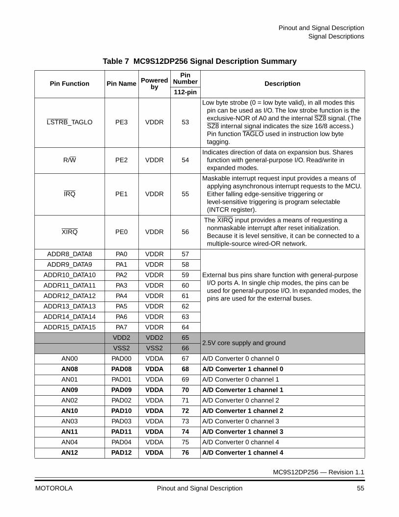
Pinout and Signal DescriptionSignal Descriptions
MC9S12DP256 — Revision 1.1
MOTOROLA Pinout and Signal Description 55
LSTRB_TAGLO PE3 VDDR 53
Low byte strobe (0 = low byte valid), in all modes this pin can be used as I/O. The low strobe function is the exclusive-NOR of A0 and the internal SZ8 signal. (The SZ8 internal signal indicates the size 16/8 access.) Pin function TAGLO used in instruction low byte tagging.
R/W PE2 VDDR 54Indicates direction of data on expansion bus. Shares
function with general-purpose I/O. Read/write in expanded modes.
IRQ PE1 VDDR 55
Maskable interrupt request input provides a means of applying asynchronous interrupt requests to the MCU. Either falling edge-sensitive triggering or level-sensitive triggering is program selectable (INTCR register).
XIRQ PE0 VDDR 56
The XIRQ input provides a means of requesting a nonmaskable interrupt after reset initialization. Because it is level sensitive, it can be connected to a multiple-source wired-OR network.
ADDR8_DATA8 PA0 VDDR 57
External bus pins share function with general-purpose I/O ports A. In single chip modes, the pins can be used for general-purpose I/O. In expanded modes, the pins are used for the external buses.
ADDR9_DATA9 PA1 VDDR 58
ADDR10_DATA10 PA2 VDDR 59
ADDR11_DATA11 PA3 VDDR 60
ADDR12_DATA12 PA4 VDDR 61
ADDR13_DATA13 PA5 VDDR 62
ADDR14_DATA14 PA6 VDDR 63
ADDR15_DATA15 PA7 VDDR 64
VDD2 VDD2 652.5V core supply and ground
VSS2 VSS2 66
AN00 PAD00 VDDA 67 A/D Converter 0 channel 0
AN08 PAD08 VDDA 68 A/D Converter 1 channel 0
AN01 PAD01 VDDA 69 A/D Converter 0 channel 1
AN09 PAD09 VDDA 70 A/D Converter 1 channel 1
AN02 PAD02 VDDA 71 A/D Converter 0 channel 2
AN10 PAD10 VDDA 72 A/D Converter 1 channel 2
AN03 PAD03 VDDA 73 A/D Converter 0 channel 3
AN11 PAD11 VDDA 74 A/D Converter 1 channel 3
AN04 PAD04 VDDA 75 A/D Converter 0 channel 4
AN12 PAD12 VDDA 76 A/D Converter 1 channel 4
Table 7 MC9S12DP256 Signal Description Summary
Pin Function Pin Name Poweredby
Pin Number Description112-pin
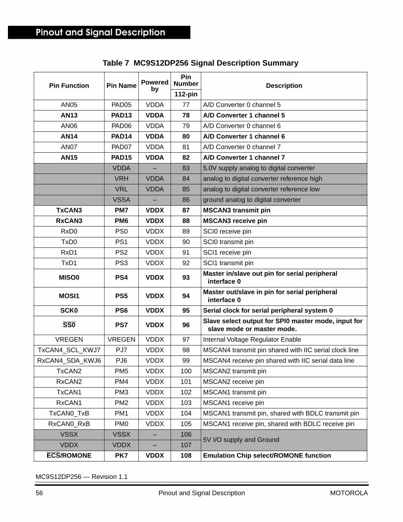
Pinout and Signal Description
MC9S12DP256 — Revision 1.1
56 Pinout and Signal Description MOTOROLA
AN05 PAD05 VDDA 77 A/D Converter 0 channel 5
AN13 PAD13 VDDA 78 A/D Converter 1 channel 5
AN06 PAD06 VDDA 79 A/D Converter 0 channel 6
AN14 PAD14 VDDA 80 A/D Converter 1 channel 6
AN07 PAD07 VDDA 81 A/D Converter 0 channel 7
AN15 PAD15 VDDA 82 A/D Converter 1 channel 7
VDDA – 83 5.0V supply analog to digital converter
VRH VDDA 84 analog to digital converter reference high
VRL VDDA 85 analog to digital converter reference low
VSSA – 86 ground analog to digital converter
TxCAN3 PM7 VDDX 87 MSCAN3 transmit pin
RxCAN3 PM6 VDDX 88 MSCAN3 receive pin
RxD0 PS0 VDDX 89 SCI0 receive pin
TxD0 PS1 VDDX 90 SCI0 transmit pin
RxD1 PS2 VDDX 91 SCI1 receive pin
TxD1 PS3 VDDX 92 SCI1 transmit pin
MISO0 PS4 VDDX 93Master in/slave out pin for serial peripheral
interface 0
MOSI1 PS5 VDDX 94Master out/slave in pin for serial peripheral
interface 0
SCK0 PS6 VDDX 95 Serial clock for serial peripheral system 0
SS0 PS7 VDDX 96Slave select output for SPI0 master mode, input for
slave mode or master mode.
VREGEN VREGEN VDDX 97 Internal Voltage Regulator Enable
TxCAN4_SCL_KWJ7 PJ7 VDDX 98 MSCAN4 transmit pin shared with IIC serial clock line
RxCAN4_SDA_KWJ6 PJ6 VDDX 99 MSCAN4 receive pin shared with IIC serial data line
TxCAN2 PM5 VDDX 100 MSCAN2 transmit pin
RxCAN2 PM4 VDDX 101 MSCAN2 receive pin
TxCAN1 PM3 VDDX 102 MSCAN1 transmit pin
RxCAN1 PM2 VDDX 103 MSCAN1 receive pin
TxCAN0_TxB PM1 VDDX 104 MSCAN1 transmit pin, shared with BDLC transmit pin
RxCAN0_RxB PM0 VDDX 105 MSCAN1 receive pin, shared with BDLC receive pin
VSSX VSSX – 1065V I/O supply and Ground
VDDX VDDX – 107
ECS/ROMONE PK7 VDDX 108 Emulation Chip select/ROMONE function
Table 7 MC9S12DP256 Signal Description Summary
Pin Function Pin Name Poweredby
Pin Number Description112-pin
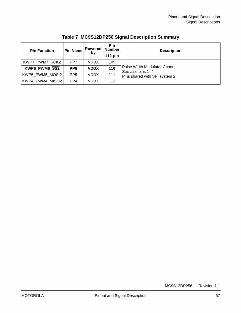
Pinout and Signal DescriptionSignal Descriptions
MC9S12DP256 — Revision 1.1
MOTOROLA Pinout and Signal Description 57
KWP7_PWM7_SCK2 PP7 VDDX 109Pulse Width Modulator ChannelSee also pins 1–4Pins shared with SPI system 2
KWP6_PWM6_SS2 PP6 VDDX 110
KWP5_PWM5_MOSI2 PP5 VDDX 111
KWP4_PWM4_MISO2 PP4 VDDX 112
Table 7 MC9S12DP256 Signal Description Summary
Pin Function Pin Name Poweredby
Pin Number Description112-pin
Pinout and Signal Description
MC9S12DP256 — Revision 1.1
58 Pinout and Signal Description MOTOROLA
Port Signals
The MC9S12DP256 incorporates eleven ports which are used to control and access the various device subsystems. When not used for these purposes, port pins may be used for general-purpose I/O. In addition to the pins described below, each port consists of a data register which can be read and written at any time, and, with the exception of port AD0, port AD1, and PE[1:0] a data direction register which controls the direction of each pin. After reset all general purpose I/O pins are configured as input.
Port A Port A bits 7 through 0 are associated with address lines A15 through A8 respectively and data lines D15/D7 through D8/D0 respectively. When this port is not used for external addresses such as in single-chip mode, these pins can be used as general purpose I/O. Data Direction Register A (DDRA) determines the primary direction of each pin. DDRA also determines the source of data for a read of PORTA.
Register DDRA determines whether each port A pin is an input or output. DDRA is not in the address map during expanded and peripheral mode operation. Setting a bit in DDRA makes the corresponding bit in port A an output; clearing a bit in DDRA makes the corresponding bit in port A an input. The default reset state of DDRA is all zeroes.
This register is not in the on-chip map in expanded and peripheral modes.
Port B Port B bits 7 through 0 are associated with address lines A7 through A0 respectively and data lines D7 through D0 respectively. When this port is not used for external addresses, such as in single-chip mode, these pins can be used as general purpose I/O. Data Direction Register B (DDRB) determines the primary direction of each pin. DDRB also determines the source of data for a read of PORTB.
Register DDRB determines whether each port B pin is an input or output. DDRB is not in the address map during expanded and peripheral mode operation. Setting a bit in DDRB makes the corresponding bit in port B
Pinout and Signal DescriptionPort Signals
MC9S12DP256 — Revision 1.1
MOTOROLA Pinout and Signal Description 59
an output; clearing a bit in DDRB makes the corresponding bit in port B an input. The default reset state of DDRB is all zeroes.
This register is not in the on-chip map in expanded and peripheral modes.
Port E Port E is associated with external bus control signals and interrupt inputs. These include mode select (PE7/NOACC/XCLKS, PE6/MODB/IPIPE1, PE5/MODA/IPIPE0), E clock, size (LSTRB/TAGLO), read / write (R/W), IRQ, and XIRQ. When the associated pin is not used for one of these specific functions, the pin can be used as general purpose I/O with the exception of IRQ and XIRQ. The Port E Assignment Register (PEAR) selects the function of each pin and DDRE determines whether each pin is an input or output when it is configured to be general purpose I/O. DDRE also determines the source of data for a read of PORTE.
Some of these pins have software selectable pullups (NOACC, ECLK, LSTRB, R/W, IRQ and XIRQ). A single control bit enables the pullups for all of these pins when they are configured as inputs.
This register is not in the on-chip map in peripheral mode or in expanded modes when the EME bit is set.
Port K This port is associated with the internal memory expansion emulation pins. When the port is not enabled to emulate the internal memory expansion, the port pins are used as general-purpose I/O. This register is not in the map in peripheral mode or in expanded modes while the EMK bit in the MODE register is set.
When inputs, these pins can be selected to be high impedance or pulled up, based upon the state of the PUPKE bit in the PUCR register.
Register DDRK determines whether each port K pin is an input or output when configured as general-purpose I/O. DDRK is not in the address map during expanded and peripheral mode operation with EMK set. Setting a bit in DDRK makes the corresponding bit in port K an output;
Pinout and Signal Description
MC9S12DP256 — Revision 1.1
60 Pinout and Signal Description MOTOROLA
clearing a bit in DDRK makes the corresponding bit in port K an input. The default reset state of DDRK is all zeroes.
NOTE: The ports H, J, M, P, S, T can be configured in a very flexible way. For a full and detailed overview refer to Section Port Integration Module.
Port M for MSCAN and BDLC
There are four identical MSCAN ports and a BDLC module sharing the multiplex port M. The port pins act as general purpose I/O if MSCAN and BDLC are disabled.
ATD PORT This port is an analog input interface to the analog-to-digital subsystem. The digital function of the ports must explicitly be enabled on per pin basis using a control register in the ADC module. When the port data registers are read, they contain the digital levels appearing on the input pins at the time of the read. Input pins with signal potentials not meeting VIL or VIH specifications will have an indeterminate value.
Use of any ATD port pin except ETRIG for digital input does not preclude the use of any other port pin for analog input. Note that the digital/analog multiplexing function is performed in the input pad. The port registers are connected to the input pads through tristate buffers. These buffers are only activated when the port is configured as digital pin so that analog signal potentials on the input pins will not cause the buffers to draw excess supply current.
Port S for SCI0, SCI1 and SPI0
There are two identical SCI ports. Each SCI module uses two external pins. The RxD0, RxD1 and TxD0, TxD1pins share general purpose port SCI P[3:0]. TxD0, TxD1 are available for general-purpose I/O when it is not configured for transmitter operation. RxD0, RxD1 are available for general-purpose I/O when it is not configured for receiver operation.
The SPI0 module uses four external pins. SS0, SCK0, MOSI0, and MISO0 pins share general purpose port PS[7:4].
Timer Port The timer module has eight external pins: PT[7:0]_IOC[7:0], for input capture and output compare functions. Two of the pins are also the pulse
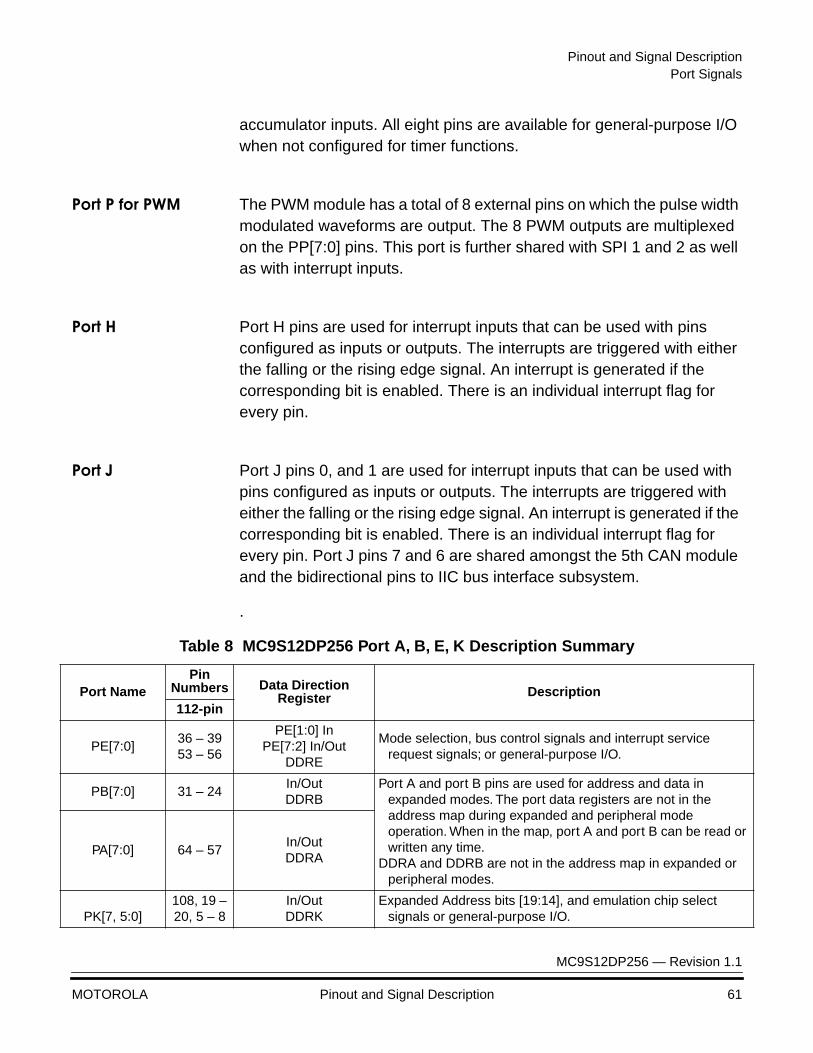
Pinout and Signal DescriptionPort Signals
MC9S12DP256 — Revision 1.1
MOTOROLA Pinout and Signal Description 61
accumulator inputs. All eight pins are available for general-purpose I/O when not configured for timer functions.
Port P for PWM The PWM module has a total of 8 external pins on which the pulse width modulated waveforms are output. The 8 PWM outputs are multiplexed on the PP[7:0] pins. This port is further shared with SPI 1 and 2 as well as with interrupt inputs.
Port H Port H pins are used for interrupt inputs that can be used with pins configured as inputs or outputs. The interrupts are triggered with either the falling or the rising edge signal. An interrupt is generated if the corresponding bit is enabled. There is an individual interrupt flag for every pin.
Port J Port J pins 0, and 1 are used for interrupt inputs that can be used with pins configured as inputs or outputs. The interrupts are triggered with either the falling or the rising edge signal. An interrupt is generated if the corresponding bit is enabled. There is an individual interrupt flag for every pin. Port J pins 7 and 6 are shared amongst the 5th CAN module and the bidirectional pins to IIC bus interface subsystem.
.
Table 8 MC9S12DP256 Port A, B, E, K Description Summary
Port NamePin
Numbers Data Direction Register Description
112-pin
PE[7:0]36 – 3953 – 56
PE[1:0] InPE[7:2] In/Out
DDRE
Mode selection, bus control signals and interrupt service request signals; or general-purpose I/O.
PB[7:0] 31 – 24In/OutDDRB
Port A and port B pins are used for address and data in expanded modes. The port data registers are not in the address map during expanded and peripheral mode operation. When in the map, port A and port B can be read or written any time.
DDRA and DDRB are not in the address map in expanded or peripheral modes.
PA[7:0] 64 – 57In/OutDDRA
PK[7, 5:0]108, 19 – 20, 5 – 8
In/OutDDRK
Expanded Address bits [19:14], and emulation chip select signals or general-purpose I/O.

Pinout and Signal Description
MC9S12DP256 — Revision 1.1
62 Pinout and Signal Description MOTOROLA
Port Pull-Up Pull-Down and Reduced Drive
MCU ports can be configured for internal pull-up. To reduce power consumption and RFI, the pin output drivers can be configured to operate at a reduced drive level. Reduced drive causes a slight increase in transition time depending on loading and should be used only for ports which have a light loading. Table 9 summarizes the port pull-up default status and controls.
Table 9 Port A, B, E, K, PAD0&1 Pull-Up, Pull-Down and Reduced Drive Summary
Enable Bit Reduced Drive Control BitPort
NameResistive
Input LoadsRegister
(Address) Bit Name Reset State
Register(Address) Bit Name Reset
State
Port A Pull-upPUCR
($000C)PUPA Disabled
RDRIV($000D)
RDPA Full drive
Port B Pull-upPUCR
($000C)PUPB Disabled
RDRIV($000D)
RDPB Full drive
Port E:
PE7, PE[4:0] Pull-upPUCR
($000C)PUPE Enabled
RDRIV ($000D)
RDPE Full drive
PE[6:5] Pull-down — — EnabledRDRIV ($000D)
RDPE Full drive
Port K[7], Port K[5:0]
Pull-upPUCR
($000C)PUPKE Enabled
RDRIV ($000D)
RDPK Full drive
Port ATD0[7:0] None —Port ATD1[7:0] None —
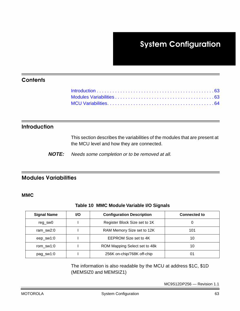
MC9S12DP256 — Revision 1.1
MOTOROLA System Configuration 63
System ConfigurationSystem Configuration
Contents
Introduction . . . . . . . . . . . . . . . . . . . . . . . . . . . . . . . . . . . . . . . . . . . . . 63Modules Variabilities . . . . . . . . . . . . . . . . . . . . . . . . . . . . . . . . . . . . . . 63MCU Variabilities. . . . . . . . . . . . . . . . . . . . . . . . . . . . . . . . . . . . . . . . . 64
Introduction
This section describes the variabilities of the modules that are present at the MCU level and how they are connected.
NOTE: Needs some completion or to be removed at all.
Modules Variabilities
MMC
The information is also readable by the MCU at address $1C, $1D (MEMSIZ0 and MEMSIZ1)
Table 10 MMC Module Variable I/O Signals
Signal Name I/O Configuration Description Connected to
reg_sw0 I Register Block Size set to 1K 0
ram_sw2:0 I RAM Memory Size set to 12K 101
eep_sw1:0 I EEPROM Size set to 4K 10
rom_sw1:0 I ROM Mapping Select set to 48k 10
pag_sw1:0 I 256K on-chip/768K off-chip 01
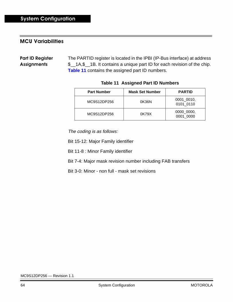
System ConÞguration
MC9S12DP256 — Revision 1.1
64 System Configuration MOTOROLA
MCU Variabilities
Part ID Register Assignments
The PARTID register is located in the IPBI (IP-Bus interface) at address $__1A,$__1B. It contains a unique part ID for each revision of the chip. Table 11 contains the assigned part ID numbers.
The coding is as follows:
Bit 15-12: Major Family identifier
Bit 11-8 : Minor Family identifier
Bit 7-4: Major mask revision number including FAB transfers
Bit 3-0: Minor - non full - mask set revisions
Table 11 Assigned Part ID Numbers
Part Number Mask Set Number PARTID
MC9S12DP256 0K36N0001_0010, 0101_0110
MC9S12DP256 0K79X0000_0000, 0001_0000

MC9S12DP256 — Revision 1.1
MOTOROLA Registers 65
RegistersRegisters
Contents
Register Block . . . . . . . . . . . . . . . . . . . . . . . . . . . . . . . . . . . . . . . . . . . 65
Register Block
The register block can be mapped to any 2K byte boundary within the first 32K byte of the standard 64K byte address space by manipulating bits REG[14:11] in the INITRG register. INITRG establishes the upper five bits of the register block’s 16-bit address. The register block occupies 1K byte. Default addressing (after reset) is indicated in the table below.
Reserved Registers The reserved registers in this register block return logic zero when read. Writes to these registers have no effect.
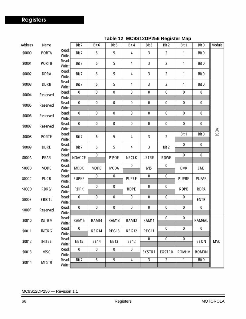
Registers
MC9S12DP256 — Revision 1.1
66 Registers MOTOROLA
Table 12 MC9S12DP256 Register MapAddress Name Bit 7 Bit 6 Bit 5 Bit 4 Bit 3 Bit 2 Bit 1 Bit 0 Module
$0000 PORTARead:
Bit 7 6 5 4 3 2 1 Bit 0
MEBI
Write:
$0001 PORTBRead:
Bit 7 6 5 4 3 2 1 Bit 0Write:
$0002 DDRARead:
Bit 7 6 5 4 3 2 1 Bit 0Write:
$0003 DDRBRead:
Bit 7 6 5 4 3 2 1 Bit 0Write:
$0004 ReservedRead: 0 0 0 0 0 0 0 0Write:
$0005 ReservedRead: 0 0 0 0 0 0 0 0Write:
$0006 ReservedRead: 0 0 0 0 0 0 0 0Write:
$0007 ReservedRead: 0 0 0 0 0 0 0 0Write:
$0008 PORTERead:
Bit 7 6 5 4 3 2Bit 1 Bit 0
Write:
$0009 DDRERead:
Bit 7 6 5 4 3 Bit 20 0
Write:
$000A PEARRead:
NOACCE 0
PIPOE NECLK LSTRE RDWE0 0
Write:
$000B MODERead:
MODC MODB MODA0
IVIS0
EMK EMEWrite:
$000C PUCRRead:
PUPKE0 0
PUPEE0 0
PUPBE PUPAEWrite:
$000D RDRIVRead:
RDPK0 0
RDPE0 0
RDPB RDPAWrite:
$000E EBICTLRead: 0 0 0 0 0 0 0
ESTRWrite:
$000F ReservedRead: 0 0 0 0 0 0 0 0Write:
$0010 INITRMRead:
RAM15 RAM14 RAM13 RAM12 RAM110 0
RAMHAL
MMC
Write:
$0011 INITRGRead: 0
REG14 REG13 REG12 REG110 0 0
Write:
$0012 INITEERead:
EE15 EE14 EE13 EE120 0 0
EEONWrite:
$0013 MISCRead: 0 0 0 0
EXSTR1 EXSTR0 ROMHM ROMONWrite:
$0014 MTST0Read: Bit 7 6 5 4 3 2 1 Bit 0Write:
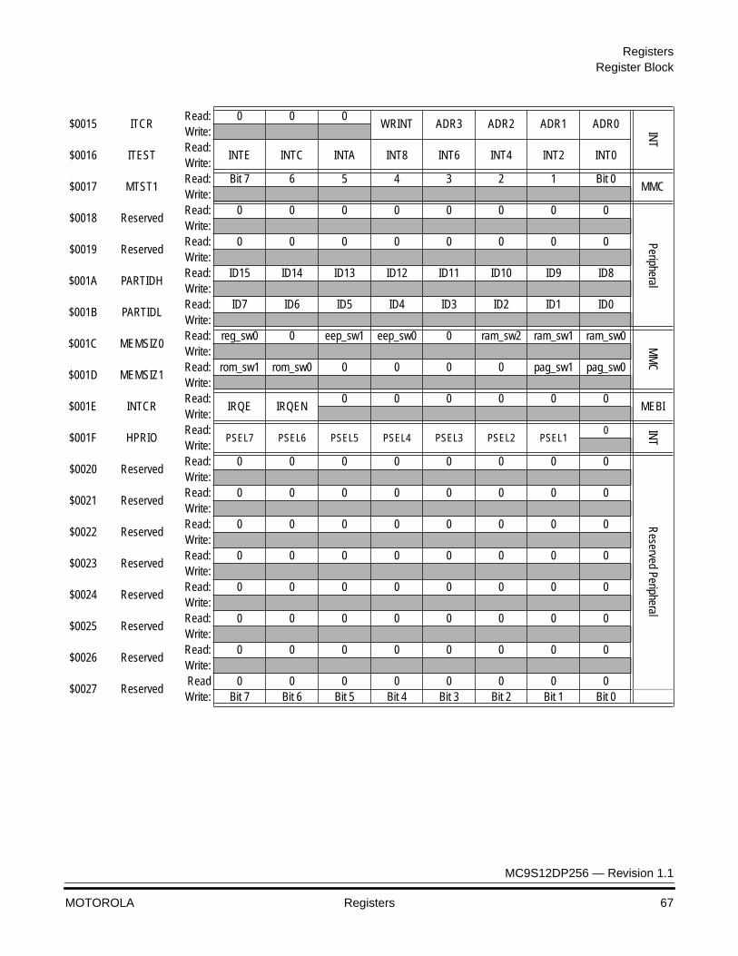
RegistersRegister Block
MC9S12DP256 — Revision 1.1
MOTOROLA Registers 67
$0015 ITCRRead: 0 0 0
WRINT ADR3 ADR2 ADR1 ADR0 INTWrite:
$0016 ITESTRead:
INTE INTC INTA INT8 INT6 INT4 INT2 INT0Write:
$0017 MTST1Read: Bit 7 6 5 4 3 2 1 Bit 0
MMCWrite:
$0018 ReservedRead: 0 0 0 0 0 0 0 0
Peripheral
Write:
$0019 ReservedRead: 0 0 0 0 0 0 0 0Write:
$001A PARTIDHRead: ID15 ID14 ID13 ID12 ID11 ID10 ID9 ID8Write:
$001B PARTIDLRead: ID7 ID6 ID5 ID4 ID3 ID2 ID1 ID0Write:
$001C MEMSIZ0Read: reg_sw0 0 eep_sw1 eep_sw0 0 ram_sw2 ram_sw1 ram_sw0
MM
C
Write:
$001D MEMSIZ1Read: rom_sw1 rom_sw0 0 0 0 0 pag_sw1 pag_sw0Write:
$001E INTCRRead:
IRQE IRQEN0 0 0 0 0 0
MEBIWrite:
$001F HPRIORead:
PSEL7 PSEL6 PSEL5 PSEL4 PSEL3 PSEL2 PSEL10 IN
T
Write:
$0020 ReservedRead: 0 0 0 0 0 0 0 0
Reserved Peripheral
Write:
$0021 ReservedRead: 0 0 0 0 0 0 0 0Write:
$0022 ReservedRead: 0 0 0 0 0 0 0 0Write:
$0023 ReservedRead: 0 0 0 0 0 0 0 0Write:
$0024 ReservedRead: 0 0 0 0 0 0 0 0Write:
$0025 ReservedRead: 0 0 0 0 0 0 0 0Write:
$0026 ReservedRead: 0 0 0 0 0 0 0 0Write:
$0027 ReservedRead 0 0 0 0 0 0 0 0Write: Bit 7 Bit 6 Bit 5 Bit 4 Bit 3 Bit 2 Bit 1 Bit 0
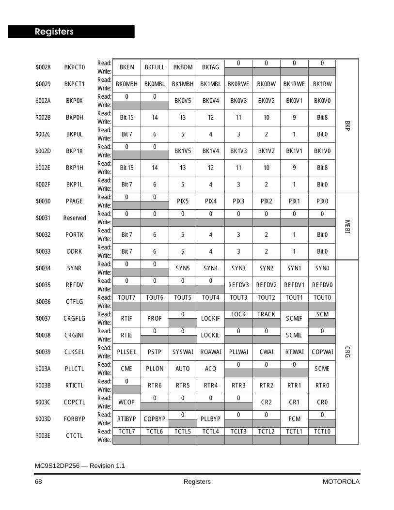
Registers
MC9S12DP256 — Revision 1.1
68 Registers MOTOROLA
$0028 BKPCT0Read:
BKEN BKFULL BKBDM BKTAG0 0 0 0
BKP
Write:
$0029 BKPCT1Read:
BK0MBH BK0MBL BK1MBH BK1MBL BK0RWE BK0RW BK1RWE BK1RWWrite:
$002A BKP0XRead: 0 0
BK0V5 BK0V4 BK0V3 BK0V2 BK0V1 BK0V0Write:
$002B BKP0HRead:
Bit 15 14 13 12 11 10 9 Bit 8Write:
$002C BKP0LRead:
Bit 7 6 5 4 3 2 1 Bit 0Write:
$002D BKP1XRead: 0 0
BK1V5 BK1V4 BK1V3 BK1V2 BK1V1 BK1V0Write:
$002E BKP1HRead:
Bit 15 14 13 12 11 10 9 Bit 8Write:
$002F BKP1LRead:
Bit 7 6 5 4 3 2 1 Bit 0Write:
$0030 PPAGERead: 0 0
PIX5 PIX4 PIX3 PIX2 PIX1 PIX0
MEBI
Write:
$0031 ReservedRead: 0 0 0 0 0 0 0 0Write:
$0032 PORTKRead:
Bit 7 6 5 4 3 2 1 Bit 0Write:
$0033 DDRKRead:
Bit 7 6 5 4 3 2 1 Bit 0Write:
$0034 SYNRRead: 0 0
SYN5 SYN4 SYN3 SYN2 SYN1 SYN0
CR
G
Write:
$0035 REFDVRead: 0 0 0 0
REFDV3 REFDV2 REFDV1 REFDV0Write:
$0036 CTFLGRead: TOUT7 TOUT6 TOUT5 TOUT4 TOUT3 TOUT2 TOUT1 TOUT0Write:
$0037 CRGFLGRead:
RTIF PROF0
LOCKIFLOCK TRACK
SCMIFSCM
Write:
$0038 CRGINTRead:
RTIE0 0
LOCKIE0 0
SCMIE0
Write:
$0039 CLKSELRead:
PLLSEL PSTP SYSWAI ROAWAI PLLWAI CWAI RTIWAI COPWAIWrite:
$003A PLLCTLRead:
CME PLLON AUTO ACQ0 0 0
SCMEWrite:
$003B RTICTLRead: 0
RTR6 RTR5 RTR4 RTR3 RTR2 RTR1 RTR0Write:
$003C COPCTLRead:
WCOP0 0 0 0
CR2 CR1 CR0Write:
$003D FORBYPRead:
RTIBYP COPBYP0
PLLBYP0 0
FCM0
Write:
$003E CTCTLRead: TCTL7 TCTL6 TCTL5 TCTL4 TCLT3 TCTL2 TCTL1 TCTL0Write:
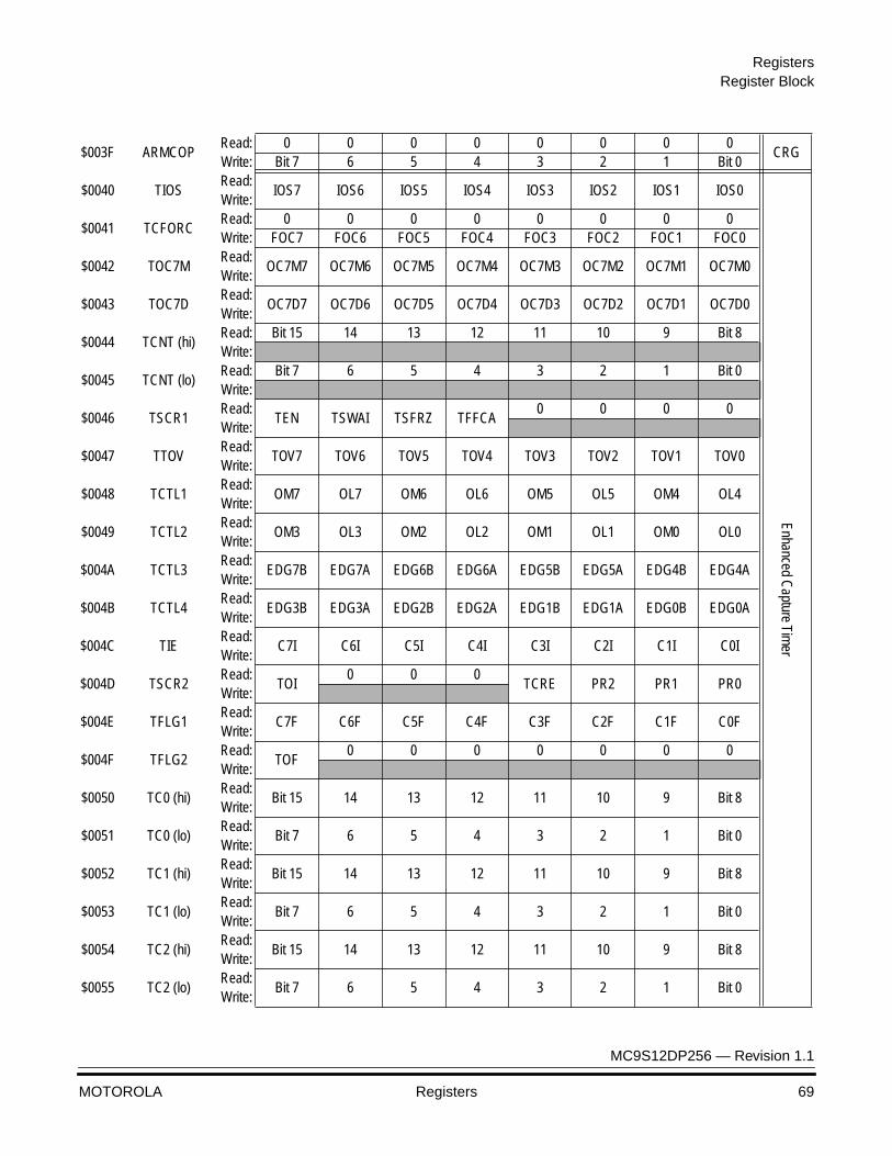
RegistersRegister Block
MC9S12DP256 — Revision 1.1
MOTOROLA Registers 69
$003F ARMCOPRead: 0 0 0 0 0 0 0 0
CRGWrite: Bit 7 6 5 4 3 2 1 Bit 0
$0040 TIOSRead:
IOS7 IOS6 IOS5 IOS4 IOS3 IOS2 IOS1 IOS0
Enhanced Capture Tim
er
Write:
$0041 TCFORCRead: 0 0 0 0 0 0 0 0Write: FOC7 FOC6 FOC5 FOC4 FOC3 FOC2 FOC1 FOC0
$0042 TOC7MRead:
OC7M7 OC7M6 OC7M5 OC7M4 OC7M3 OC7M2 OC7M1 OC7M0Write:
$0043 TOC7DRead:
OC7D7 OC7D6 OC7D5 OC7D4 OC7D3 OC7D2 OC7D1 OC7D0Write:
$0044 TCNT (hi)Read: Bit 15 14 13 12 11 10 9 Bit 8Write:
$0045 TCNT (lo)Read: Bit 7 6 5 4 3 2 1 Bit 0Write:
$0046 TSCR1Read:
TEN TSWAI TSFRZ TFFCA0 0 0 0
Write:
$0047 TTOVRead:
TOV7 TOV6 TOV5 TOV4 TOV3 TOV2 TOV1 TOV0Write:
$0048 TCTL1Read:
OM7 OL7 OM6 OL6 OM5 OL5 OM4 OL4Write:
$0049 TCTL2Read:
OM3 OL3 OM2 OL2 OM1 OL1 OM0 OL0Write:
$004A TCTL3Read:
EDG7B EDG7A EDG6B EDG6A EDG5B EDG5A EDG4B EDG4AWrite:
$004B TCTL4Read:
EDG3B EDG3A EDG2B EDG2A EDG1B EDG1A EDG0B EDG0AWrite:
$004C TIERead:
C7I C6I C5I C4I C3I C2I C1I C0IWrite:
$004D TSCR2Read:
TOI0 0 0
TCRE PR2 PR1 PR0Write:
$004E TFLG1Read:
C7F C6F C5F C4F C3F C2F C1F C0FWrite:
$004F TFLG2Read:
TOF0 0 0 0 0 0 0
Write:
$0050 TC0 (hi)Read:
Bit 15 14 13 12 11 10 9 Bit 8Write:
$0051 TC0 (lo)Read:
Bit 7 6 5 4 3 2 1 Bit 0Write:
$0052 TC1 (hi)Read:
Bit 15 14 13 12 11 10 9 Bit 8Write:
$0053 TC1 (lo)Read:
Bit 7 6 5 4 3 2 1 Bit 0Write:
$0054 TC2 (hi)Read:
Bit 15 14 13 12 11 10 9 Bit 8Write:
$0055 TC2 (lo)Read:
Bit 7 6 5 4 3 2 1 Bit 0Write:
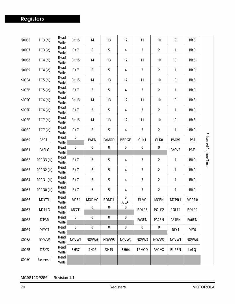
Registers
MC9S12DP256 — Revision 1.1
70 Registers MOTOROLA
$0056 TC3 (hi)Read:
Bit 15 14 13 12 11 10 9 Bit 8
Enhanced Capture Tim
er
Write:
$0057 TC3 (lo)Read:
Bit 7 6 5 4 3 2 1 Bit 0Write:
$0058 TC4 (hi)Read:
Bit 15 14 13 12 11 10 9 Bit 8Write:
$0059 TC4 (lo)Read:
Bit 7 6 5 4 3 2 1 Bit 0Write:
$005A TC5 (hi)Read:
Bit 15 14 13 12 11 10 9 Bit 8Write:
$005B TC5 (lo)Read:
Bit 7 6 5 4 3 2 1 Bit 0Write:
$005C TC6 (hi)Read:
Bit 15 14 13 12 11 10 9 Bit 8Write:
$005D TC6 (lo)Read:
Bit 7 6 5 4 3 2 1 Bit 0Write:
$005E TC7 (hi)Read:
Bit 15 14 13 12 11 10 9 Bit 8Write:
$005F TC7 (lo)Read:
Bit 7 6 5 4 3 2 1 Bit 0Write:
$0060 PACTLRead: 0
PAEN PAMOD PEDGE CLK1 CLK0 PAOVI PAIWrite:
$0061 PAFLGRead: 0 0 0 0 0 0
PAOVF PAIFWrite:
$0062 PACN3 (hi)Read:
Bit 7 6 5 4 3 2 1 Bit 0Write:
$0063 PACN2 (lo)Read:
Bit 7 6 5 4 3 2 1 Bit 0Write:
$0064 PACN1 (hi)Read:
Bit 7 6 5 4 3 2 1 Bit 0Write:
$0065 PACN0 (lo)Read:
Bit 7 6 5 4 3 2 1 Bit 0Write:
$0066 MCCTLRead:
MCZI MODMC RDMCL0
FLMC MCEN MCPR1 MCPR0Write: ICLAT
$0067 MCFLGRead:
MCZF0 0 0
POLF3 POLF2 POLF1 POLF0Write:
$0068 ICPARRead: 0 0 0 0
PA3EN PA2EN PA1EN PA0ENWrite:
$0069 DLYCTRead: 0 0 0 0 0 0
DLY1 DLY0Write:
$006A ICOVWRead:
NOVW7 NOVW6 NOVW5 NOVW4 NOVW3 NOVW2 NOVW1 NOVW0Write:
$006B ICSYSRead:
SH37 SH26 SH15 SH04 TFMOD PACMX BUFEN LATQWrite:
$006C ReservedRead:Write:
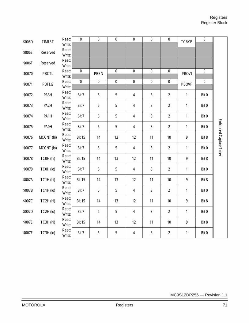
RegistersRegister Block
MC9S12DP256 — Revision 1.1
MOTOROLA Registers 71
$006D TIMTSTRead: 0 0 0 0 0 0
TCBYP0
Enhanced Capture Tim
er
Write:
$006E ReservedRead:Write:
$006F ReservedRead:Write:
$0070 PBCTLRead: 0
PBEN0 0 0 0
PBOVI0
Write:
$0071 PBFLGRead: 0 0 0 0 0 0
PBOVF0
Write:
$0072 PA3HRead:
Bit 7 6 5 4 3 2 1 Bit 0Write:
$0073 PA2HRead:
Bit 7 6 5 4 3 2 1 Bit 0Write:
$0074 PA1HRead:
Bit 7 6 5 4 3 2 1 Bit 0Write:
$0075 PA0HRead:
Bit 7 6 5 4 3 2 1 Bit 0Write:
$0076 MCCNT (hi)Read:
Bit 15 14 13 12 11 10 9 Bit 8Write:
$0077 MCCNT (lo)Read:
Bit 7 6 5 4 3 2 1 Bit 0Write:
$0078 TC0H (hi)Read:
Bit 15 14 13 12 11 10 9 Bit 8Write:
$0079 TC0H (lo)Read:
Bit 7 6 5 4 3 2 1 Bit 0Write:
$007A TC1H (hi)Read:
Bit 15 14 13 12 11 10 9 Bit 8Write:
$007B TC1H (lo)Read:
Bit 7 6 5 4 3 2 1 Bit 0Write:
$007C TC2H (hi)Read:
Bit 15 14 13 12 11 10 9 Bit 8Write:
$007D TC2H (lo)Read:
Bit 7 6 5 4 3 2 1 Bit 0Write:
$007E TC3H (hi)Read:
Bit 15 14 13 12 11 10 9 Bit 8Write:
$007F TC3H (lo)Read:
Bit 7 6 5 4 3 2 1 Bit 0Write:
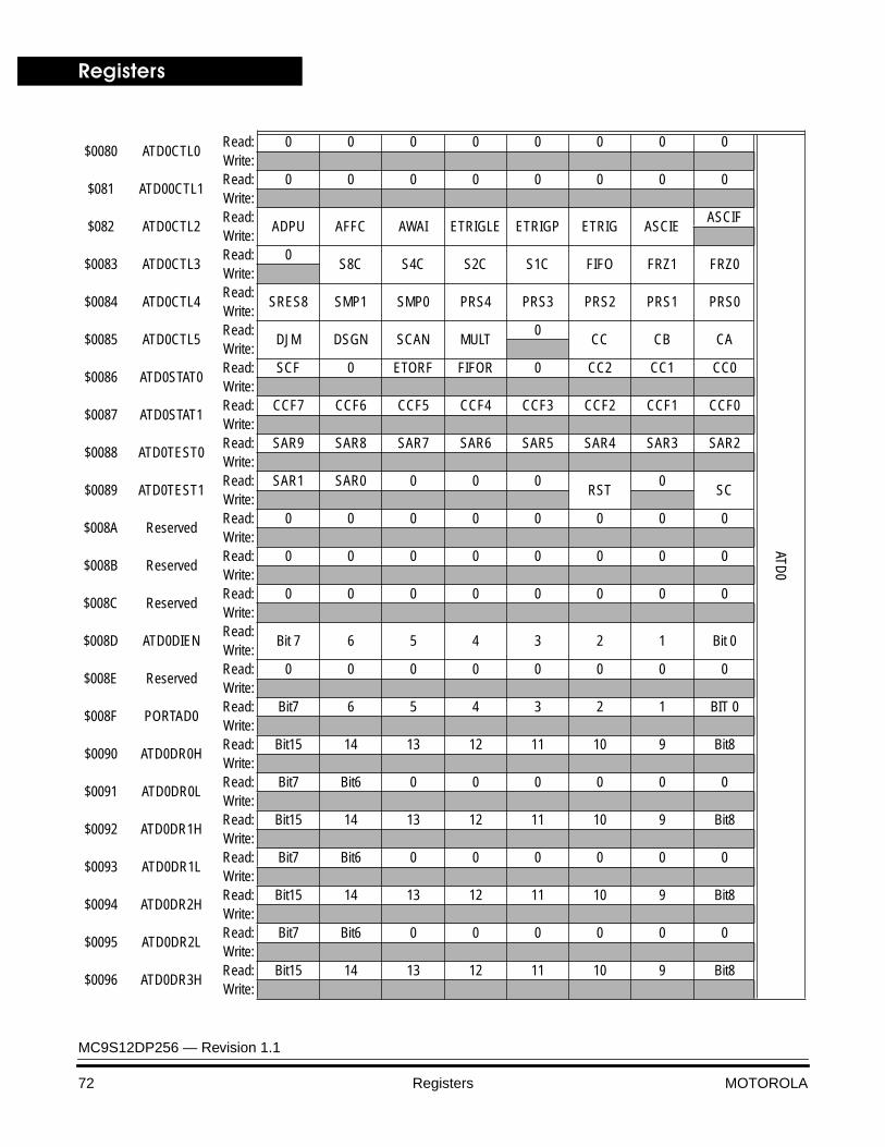
Registers
MC9S12DP256 — Revision 1.1
72 Registers MOTOROLA
$0080 ATD0CTL0Read: 0 0 0 0 0 0 0 0
ATD0
Write:
$081 ATD00CTL1Read: 0 0 0 0 0 0 0 0Write:
$082 ATD0CTL2Read:
ADPU AFFC AWAI ETRIGLE ETRIGP ETRIG ASCIEASCIF
Write:
$0083 ATD0CTL3Read: 0
S8C S4C S2C S1C FIFO FRZ1 FRZ0Write:
$0084 ATD0CTL4Read:
SRES8 SMP1 SMP0 PRS4 PRS3 PRS2 PRS1 PRS0Write:
$0085 ATD0CTL5Read:
DJM DSGN SCAN MULT0
CC CB CAWrite:
$0086 ATD0STAT0Read: SCF 0 ETORF FIFOR 0 CC2 CC1 CC0Write:
$0087 ATD0STAT1Read: CCF7 CCF6 CCF5 CCF4 CCF3 CCF2 CCF1 CCF0Write:
$0088 ATD0TEST0Read: SAR9 SAR8 SAR7 SAR6 SAR5 SAR4 SAR3 SAR2Write:
$0089 ATD0TEST1Read: SAR1 SAR0 0 0 0
RST0
SCWrite:
$008A ReservedRead: 0 0 0 0 0 0 0 0Write:
$008B ReservedRead: 0 0 0 0 0 0 0 0Write:
$008C ReservedRead: 0 0 0 0 0 0 0 0Write:
$008D ATD0DIENRead:
Bit 7 6 5 4 3 2 1 Bit 0Write:
$008E ReservedRead: 0 0 0 0 0 0 0 0Write:
$008F PORTAD0Read: Bit7 6 5 4 3 2 1 BIT 0Write:
$0090 ATD0DR0HRead: Bit15 14 13 12 11 10 9 Bit8Write:
$0091 ATD0DR0LRead: Bit7 Bit6 0 0 0 0 0 0Write:
$0092 ATD0DR1HRead: Bit15 14 13 12 11 10 9 Bit8Write:
$0093 ATD0DR1LRead: Bit7 Bit6 0 0 0 0 0 0Write:
$0094 ATD0DR2HRead: Bit15 14 13 12 11 10 9 Bit8Write:
$0095 ATD0DR2LRead: Bit7 Bit6 0 0 0 0 0 0Write:
$0096 ATD0DR3HRead: Bit15 14 13 12 11 10 9 Bit8Write:
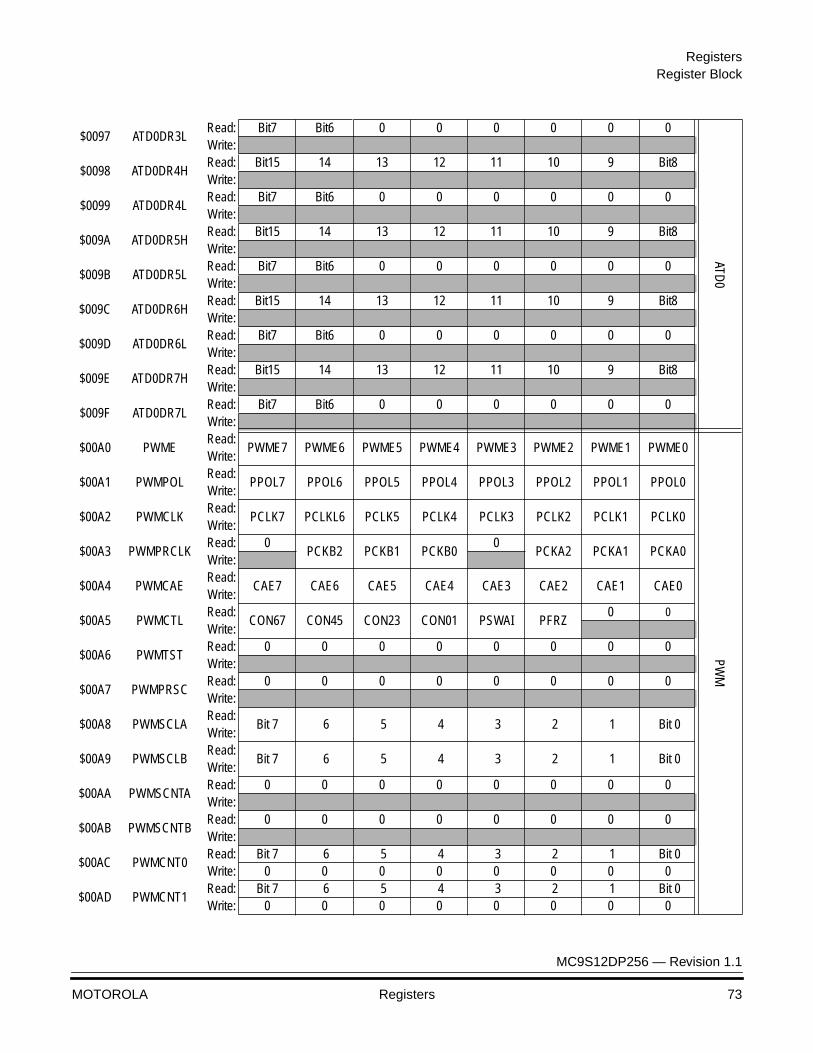
RegistersRegister Block
MC9S12DP256 — Revision 1.1
MOTOROLA Registers 73
$0097 ATD0DR3LRead: Bit7 Bit6 0 0 0 0 0 0
ATD0
Write:
$0098 ATD0DR4HRead: Bit15 14 13 12 11 10 9 Bit8Write:
$0099 ATD0DR4LRead: Bit7 Bit6 0 0 0 0 0 0Write:
$009A ATD0DR5HRead: Bit15 14 13 12 11 10 9 Bit8Write:
$009B ATD0DR5LRead: Bit7 Bit6 0 0 0 0 0 0Write:
$009C ATD0DR6HRead: Bit15 14 13 12 11 10 9 Bit8Write:
$009D ATD0DR6LRead: Bit7 Bit6 0 0 0 0 0 0Write:
$009E ATD0DR7HRead: Bit15 14 13 12 11 10 9 Bit8Write:
$009F ATD0DR7LRead: Bit7 Bit6 0 0 0 0 0 0Write:
$00A0 PWMERead:
PWME7 PWME6 PWME5 PWME4 PWME3 PWME2 PWME1 PWME0
PWM
Write:
$00A1 PWMPOLRead:
PPOL7 PPOL6 PPOL5 PPOL4 PPOL3 PPOL2 PPOL1 PPOL0Write:
$00A2 PWMCLKRead:
PCLK7 PCLKL6 PCLK5 PCLK4 PCLK3 PCLK2 PCLK1 PCLK0Write:
$00A3 PWMPRCLKRead: 0
PCKB2 PCKB1 PCKB00
PCKA2 PCKA1 PCKA0Write:
$00A4 PWMCAERead:
CAE7 CAE6 CAE5 CAE4 CAE3 CAE2 CAE1 CAE0Write:
$00A5 PWMCTLRead:
CON67 CON45 CON23 CON01 PSWAI PFRZ0 0
Write:
$00A6 PWMTSTRead: 0 0 0 0 0 0 0 0Write:
$00A7 PWMPRSCRead: 0 0 0 0 0 0 0 0Write:
$00A8 PWMSCLARead:
Bit 7 6 5 4 3 2 1 Bit 0 Write:
$00A9 PWMSCLBRead:
Bit 7 6 5 4 3 2 1 Bit 0 Write:
$00AA PWMSCNTARead: 0 0 0 0 0 0 0 0Write:
$00AB PWMSCNTBRead: 0 0 0 0 0 0 0 0Write:
$00AC PWMCNT0Read: Bit 7 6 5 4 3 2 1 Bit 0 Write: 0 0 0 0 0 0 0 0
$00AD PWMCNT1Read: Bit 7 6 5 4 3 2 1 Bit 0 Write: 0 0 0 0 0 0 0 0
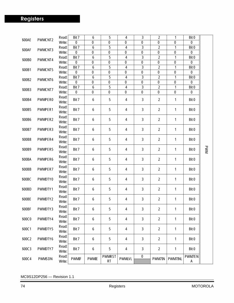
Registers
MC9S12DP256 — Revision 1.1
74 Registers MOTOROLA
$00AE PWMCNT2Read: Bit 7 6 5 4 3 2 1 Bit 0
PWM
Write: 0 0 0 0 0 0 0 0
$00AF PWMCNT3Read: Bit 7 6 5 4 3 2 1 Bit 0 Write: 0 0 0 0 0 0 0 0
$00B0 PWMCNT4Read: Bit 7 6 5 4 3 2 1 Bit 0 Write: 0 0 0 0 0 0 0 0
$00B1 PWMCNT5Read: Bit 7 6 5 4 3 2 1 Bit 0 Write: 0 0 0 0 0 0 0 0
$00B2 PWMCNT6Read: Bit 7 6 5 4 3 2 1 Bit 0 Write: 0 0 0 0 0 0 0 0
$00B3 PWMCNT7Read: Bit 7 6 5 4 3 2 1 Bit 0 Write: 0 0 0 0 0 0 0 0
$00B4 PWMPER0Read:
Bit 7 6 5 4 3 2 1 Bit 0 Write:
$00B5 PWMPER1Read:
Bit 7 6 5 4 3 2 1 Bit 0 Write:
$00B6 PWMPER2Read:
Bit 7 6 5 4 3 2 1 Bit 0 Write:
$00B7 PWMPER3Read:
Bit 7 6 5 4 3 2 1 Bit 0 Write:
$00B8 PWMPER4Read:
Bit 7 6 5 4 3 2 1 Bit 0 Write:
$00B9 PWMPER5Read:
Bit 7 6 5 4 3 2 1 Bit 0 Write:
$00BA PWMPER6Read:
Bit 7 6 5 4 3 2 1 Bit 0 Write:
$00BB PWMPER7Read:
Bit 7 6 5 4 3 2 1 Bit 0 Write:
$00BC PWMDTY0Read:
Bit 7 6 5 4 3 2 1 Bit 0 Write:
$00BD PWMDTY1Read:
Bit 7 6 5 4 3 2 1 Bit 0 Write:
$00BE PWMDTY2Read:
Bit 7 6 5 4 3 2 1 Bit 0 Write:
$00BF PWMDTY3Read:
Bit 7 6 5 4 3 2 1 Bit 0 Write:
$00C0 PWMDTY4Read:
Bit 7 6 5 4 3 2 1 Bit 0 Write:
$00C1 PWMDTY5Read:
Bit 7 6 5 4 3 2 1 Bit 0 Write:
$00C2 PWMDTY6Read:
Bit 7 6 5 4 3 2 1 Bit 0 Write:
$00C3 PWMDTY7Read:
Bit 7 6 5 4 3 2 1 Bit 0 Write:
$00C4 PWMSDNRead:
PWMIF PWMIEPWMRST
RTPWMLVL
0PWM7IN PWM7INL
PWM7ENAWrite:
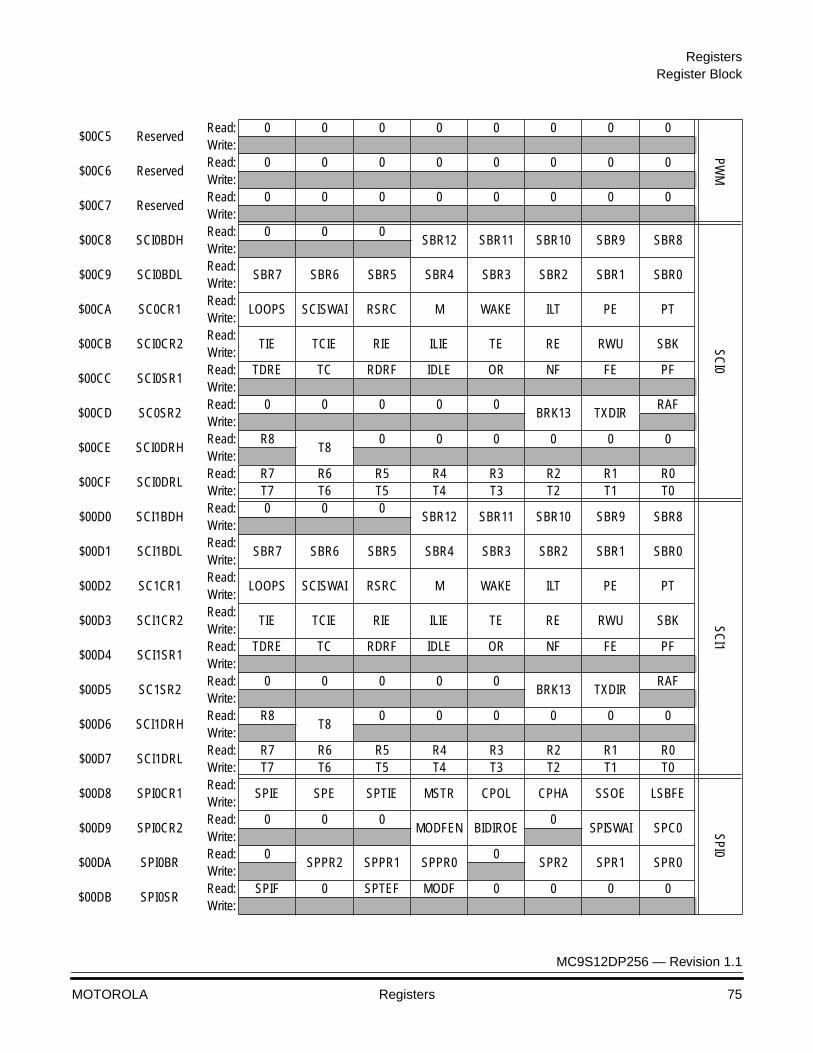
RegistersRegister Block
MC9S12DP256 — Revision 1.1
MOTOROLA Registers 75
$00C5 ReservedRead: 0 0 0 0 0 0 0 0
PWM
Write:
$00C6 ReservedRead: 0 0 0 0 0 0 0 0Write:
$00C7 ReservedRead: 0 0 0 0 0 0 0 0Write:
$00C8 SCI0BDHRead: 0 0 0
SBR12 SBR11 SBR10 SBR9 SBR8
SCI0
Write:
$00C9 SCI0BDLRead:
SBR7 SBR6 SBR5 SBR4 SBR3 SBR2 SBR1 SBR0Write:
$00CA SC0CR1Read:
LOOPS SCISWAI RSRC M WAKE ILT PE PTWrite:
$00CB SCI0CR2Read:
TIE TCIE RIE ILIE TE RE RWU SBKWrite:
$00CC SCI0SR1Read: TDRE TC RDRF IDLE OR NF FE PFWrite:
$00CD SC0SR2Read: 0 0 0 0 0
BRK13 TXDIRRAF
Write:
$00CE SCI0DRHRead: R8
T80 0 0 0 0 0
Write:
$00CF SCI0DRLRead: R7 R6 R5 R4 R3 R2 R1 R0Write: T7 T6 T5 T4 T3 T2 T1 T0
$00D0 SCI1BDHRead: 0 0 0
SBR12 SBR11 SBR10 SBR9 SBR8
SCI1
Write:
$00D1 SCI1BDLRead:
SBR7 SBR6 SBR5 SBR4 SBR3 SBR2 SBR1 SBR0Write:
$00D2 SC1CR1Read:
LOOPS SCISWAI RSRC M WAKE ILT PE PTWrite:
$00D3 SCI1CR2Read:
TIE TCIE RIE ILIE TE RE RWU SBKWrite:
$00D4 SCI1SR1Read: TDRE TC RDRF IDLE OR NF FE PFWrite:
$00D5 SC1SR2Read: 0 0 0 0 0
BRK13 TXDIRRAF
Write:
$00D6 SCI1DRHRead: R8
T80 0 0 0 0 0
Write:
$00D7 SCI1DRLRead: R7 R6 R5 R4 R3 R2 R1 R0Write: T7 T6 T5 T4 T3 T2 T1 T0
$00D8 SPI0CR1Read:
SPIE SPE SPTIE MSTR CPOL CPHA SSOE LSBFE
SPI0
Write:
$00D9 SPI0CR2Read: 0 0 0
MODFEN BIDIROE0
SPISWAI SPC0Write:
$00DA SPI0BRRead: 0
SPPR2 SPPR1 SPPR00
SPR2 SPR1 SPR0Write:
$00DB SPI0SRRead: SPIF 0 SPTEF MODF 0 0 0 0Write:
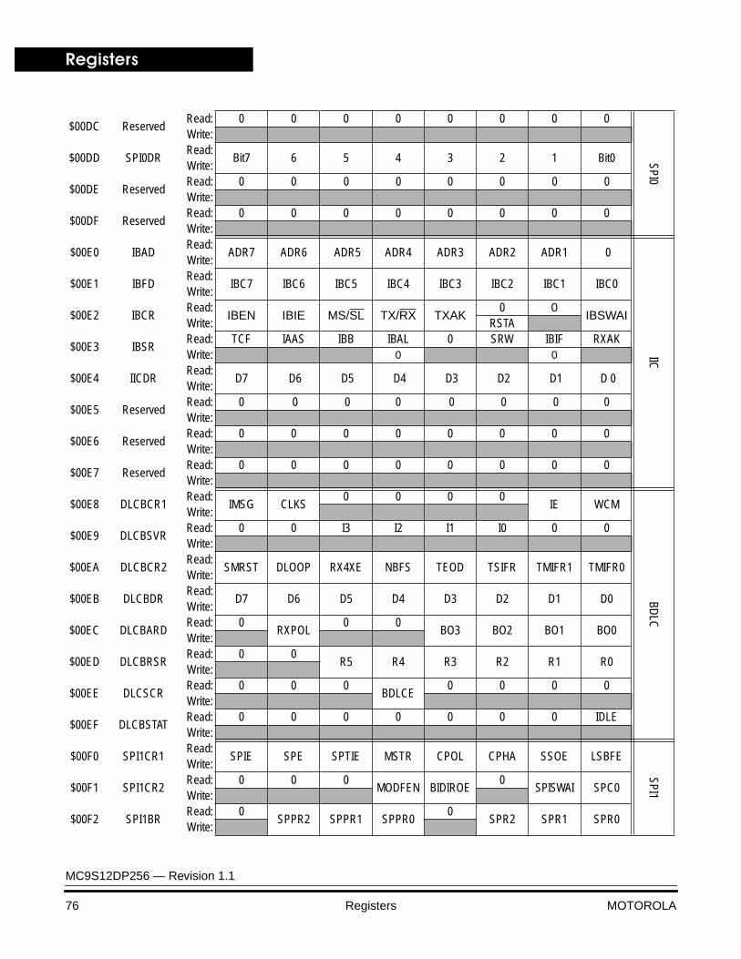
Registers
MC9S12DP256 — Revision 1.1
76 Registers MOTOROLA
$00DC ReservedRead: 0 0 0 0 0 0 0 0
SPI0
Write:
$00DD SPI0DRRead:
Bit7 6 5 4 3 2 1 Bit0Write:
$00DE ReservedRead: 0 0 0 0 0 0 0 0Write:
$00DF ReservedRead: 0 0 0 0 0 0 0 0Write:
$00E0 IBADRead:
ADR7 ADR6 ADR5 ADR4 ADR3 ADR2 ADR1 0
IIC
Write:
$00E1 IBFDRead:
IBC7 IBC6 IBC5 IBC4 IBC3 IBC2 IBC1 IBC0Write:
$00E2 IBCRRead:
IBEN IBIE MS/SL TX/RX TXAK0 0
IBSWAIWrite: RSTA
$00E3 IBSRRead: TCF IAAS IBB IBAL 0 SRW IBIF RXAKWrite: 0 0
$00E4 IICDRRead:
D7 D6 D5 D4 D3 D2 D1 D 0 Write:
$00E5 ReservedRead: 0 0 0 0 0 0 0 0Write:
$00E6 ReservedRead: 0 0 0 0 0 0 0 0Write:
$00E7 ReservedRead: 0 0 0 0 0 0 0 0Write:
$00E8 DLCBCR1Read:
IMSG CLKS0 0 0 0
IE WCM
BDLC
Write:
$00E9 DLCBSVRRead: 0 0 I3 I2 I1 I0 0 0Write:
$00EA DLCBCR2Read:
SMRST DLOOP RX4XE NBFS TEOD TSIFR TMIFR1 TMIFR0Write:
$00EB DLCBDRRead:
D7 D6 D5 D4 D3 D2 D1 D0Write:
$00EC DLCBARDRead: 0
RXPOL0 0
BO3 BO2 BO1 BO0Write:
$00ED DLCBRSRRead: 0 0
R5 R4 R3 R2 R1 R0Write:
$00EE DLCSCRRead: 0 0 0
BDLCE0 0 0 0
Write:
$00EF DLCBSTATRead: 0 0 0 0 0 0 0 IDLEWrite:
$00F0 SPI1CR1Read:
SPIE SPE SPTIE MSTR CPOL CPHA SSOE LSBFE
SPI1
Write:
$00F1 SPI1CR2Read: 0 0 0
MODFEN BIDIROE0
SPISWAI SPC0Write:
$00F2 SPI1BRRead: 0
SPPR2 SPPR1 SPPR00
SPR2 SPR1 SPR0Write:
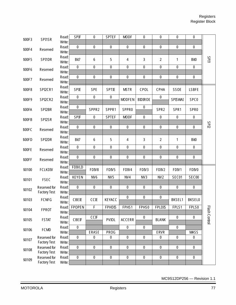
RegistersRegister Block
MC9S12DP256 — Revision 1.1
MOTOROLA Registers 77
$00F3 SPI1SRRead: SPIF 0 SPTEF MODF 0 0 0 0
SPI1
Write:
$00F4 ReservedRead: 0 0 0 0 0 0 0 0Write:
$00F5 SPI1DRRead:
Bit7 6 5 4 3 2 1 Bit0Write:
$00F6 ReservedRead: 0 0 0 0 0 0 0 0Write:
$00F7 ReservedRead: 0 0 0 0 0 0 0 0Write:
$00F8 SPI2CR1Read:
SPIE SPE SPTIE MSTR CPOL CPHA SSOE LSBFE
SPI2
Write:
$00F9 SPI2CR2Read: 0 0 0
MODFEN BIDIROE0
SPISWAI SPC0Write:
$00FA SPI2BRRead: 0
SPPR2 SPPR1 SPPR00
SPR2 SPR1 SPR0Write:
$00FB SPI2SRRead: SPIF 0 SPTEF MODF 0 0 0 0Write:
$00FC ReservedRead: 0 0 0 0 0 0 0 0Write:
$00FD SPI2DRRead:
Bit7 6 5 4 3 2 1 Bit0Write:
$00FE ReservedRead: 0 0 0 0 0 0 0 0Write:
$00FF ReservedRead: 0 0 0 0 0 0 0 0Write:
$0100 FCLKDIVRead: FDIVLD
FDIV8 FDIV5 FDIV4 FDIV3 FDIV2 FDIV1 FDIV0
Flash Control
Write:
$0101 FSECRead: KEYEN NV6 NV5 NV4 NV3 NV2 SEC01 SEC00Write:
$0102Reserved for Factory Test
Read: 0 0 0 0 0 0 0 0Write:
$0103 FCNFGRead:
CBEIE CCIE KEYACC0 0 0
BKSEL1 BKSEL0Write:
$0104 FPROTRead: FPOPEN F FPHDIS FPHS1 FPHS0 FPLDIS FPLS1 FPLS0Write:
$0105 FSTATRead:
CBEIFCCIF
PVIOL ACCERR0
BLANK0 0
Write:
$0106 FCMDRead: 0 0 0 0Write: ERASE PROG ERVR MASS
$0107Reserved for Factory Test
Read: 0 0 0 0 0 0 0 0Write:
$0108Reserved for Factory Test
Read: 0 0 0 0 0 0 0 0Write:
$0109Reserved for Factory Test
Read: 0 0 0 0 0 0 0 0Write:
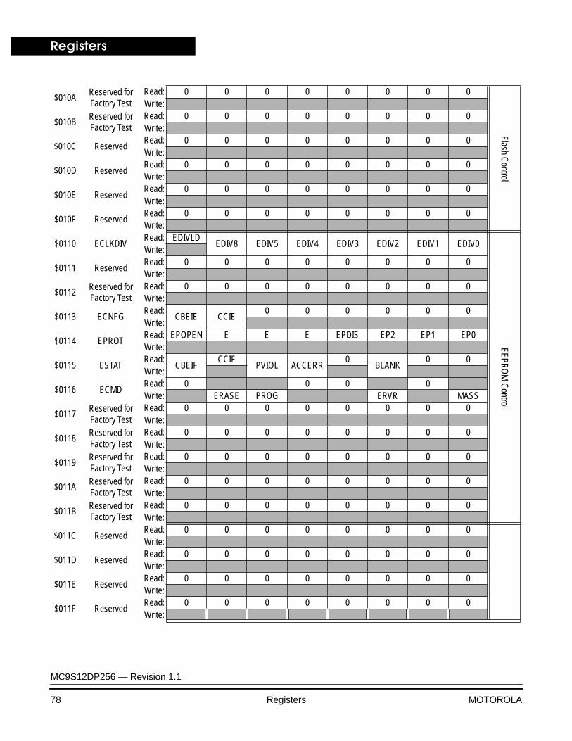
Registers
MC9S12DP256 — Revision 1.1
78 Registers MOTOROLA
$010AReserved for Factory Test
Read: 0 0 0 0 0 0 0 0
Flash Control
Write:
$010BReserved for Factory Test
Read: 0 0 0 0 0 0 0 0Write:
$010C ReservedRead: 0 0 0 0 0 0 0 0Write:
$010D ReservedRead: 0 0 0 0 0 0 0 0Write:
$010E ReservedRead: 0 0 0 0 0 0 0 0Write:
$010F ReservedRead: 0 0 0 0 0 0 0 0Write:
$0110 ECLKDIVRead: EDIVLD
EDIV8 EDIV5 EDIV4 EDIV3 EDIV2 EDIV1 EDIV0
EEPROM
Control
Write:
$0111 ReservedRead: 0 0 0 0 0 0 0 0Write:
$0112Reserved for Factory Test
Read: 0 0 0 0 0 0 0 0Write:
$0113 ECNFGRead:
CBEIE CCIE0 0 0 0 0 0
Write:
$0114 EPROTRead: EPOPEN E E E EPDIS EP2 EP1 EP0Write:
$0115 ESTATRead:
CBEIFCCIF
PVIOL ACCERR0
BLANK0 0
Write:
$0116 ECMDRead: 0 0 0 0Write: ERASE PROG ERVR MASS
$0117Reserved for Factory Test
Read: 0 0 0 0 0 0 0 0Write:
$0118Reserved for Factory Test
Read: 0 0 0 0 0 0 0 0Write:
$0119Reserved for Factory Test
Read: 0 0 0 0 0 0 0 0Write:
$011AReserved for Factory Test
Read: 0 0 0 0 0 0 0 0Write:
$011BReserved for Factory Test
Read: 0 0 0 0 0 0 0 0Write:
$011C ReservedRead: 0 0 0 0 0 0 0 0Write:
$011D ReservedRead: 0 0 0 0 0 0 0 0Write:
$011E ReservedRead: 0 0 0 0 0 0 0 0Write:
$011F ReservedRead: 0 0 0 0 0 0 0 0Write:
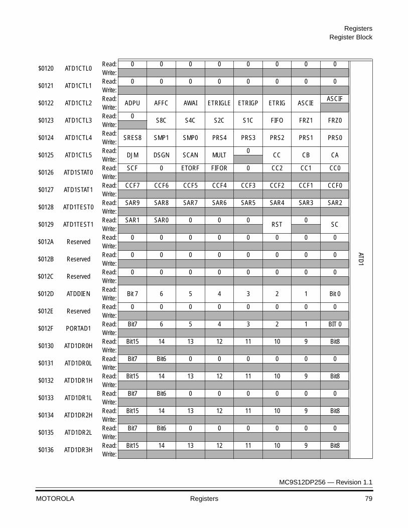
RegistersRegister Block
MC9S12DP256 — Revision 1.1
MOTOROLA Registers 79
$0120 ATD1CTL0Read: 0 0 0 0 0 0 0 0
ATD1
Write:
$0121 ATD1CTL1Read: 0 0 0 0 0 0 0 0Write:
$0122 ATD1CTL2Read:
ADPU AFFC AWAI ETRIGLE ETRIGP ETRIG ASCIEASCIF
Write:
$0123 ATD1CTL3Read: 0
S8C S4C S2C S1C FIFO FRZ1 FRZ0Write:
$0124 ATD1CTL4Read:
SRES8 SMP1 SMP0 PRS4 PRS3 PRS2 PRS1 PRS0Write:
$0125 ATD1CTL5Read:
DJM DSGN SCAN MULT0
CC CB CAWrite:
$0126 ATD1STAT0Read: SCF 0 ETORF FIFOR 0 CC2 CC1 CC0Write:
$0127 ATD1STAT1Read: CCF7 CCF6 CCF5 CCF4 CCF3 CCF2 CCF1 CCF0Write:
$0128 ATD1TEST0Read: SAR9 SAR8 SAR7 SAR6 SAR5 SAR4 SAR3 SAR2Write:
$0129 ATD1TEST1Read: SAR1 SAR0 0 0 0
RST0
SCWrite:
$012A ReservedRead: 0 0 0 0 0 0 0 0Write:
$012B ReservedRead: 0 0 0 0 0 0 0 0Write:
$012C ReservedRead: 0 0 0 0 0 0 0 0Write:
$012D ATDDIENRead:
Bit 7 6 5 4 3 2 1 Bit 0Write:
$012E ReservedRead: 0 0 0 0 0 0 0 0Write:
$012F PORTAD1Read: Bit7 6 5 4 3 2 1 BIT 0Write:
$0130 ATD1DR0HRead: Bit15 14 13 12 11 10 9 Bit8Write:
$0131 ATD1DR0LRead: Bit7 Bit6 0 0 0 0 0 0Write:
$0132 ATD1DR1HRead: Bit15 14 13 12 11 10 9 Bit8Write:
$0133 ATD1DR1LRead: Bit7 Bit6 0 0 0 0 0 0Write:
$0134 ATD1DR2HRead: Bit15 14 13 12 11 10 9 Bit8Write:
$0135 ATD1DR2LRead: Bit7 Bit6 0 0 0 0 0 0Write:
$0136 ATD1DR3HRead: Bit15 14 13 12 11 10 9 Bit8Write:

Registers
MC9S12DP256 — Revision 1.1
80 Registers MOTOROLA
$0137 ATD1DR3LRead: Bit7 Bit6 0 0 0 0 0 0
ATD1
Write:
$0138 ATD1DR4HRead: Bit15 14 13 12 11 10 9 Bit8Write:
$0139 ATD1DR4LRead: Bit7 Bit6 0 0 0 0 0 0Write:
$013A ATD1DR5HRead: Bit15 14 13 12 11 10 9 Bit8Write:
$013B ATD1DR5LRead: Bit7 Bit6 0 0 0 0 0 0Write:
$013C ATD1DR6HRead: Bit15 14 13 12 11 10 9 Bit8Write:
$013D ATD1DR6LRead: Bit7 Bit6 0 0 0 0 0 0Write:
$013E ATD1DR7HRead: Bit15 14 13 12 11 10 9 Bit8Write:
$013F ATD1DR7LRead: Bit7 Bit6 0 0 0 0 0 0Write:
$0140 CAN0CTL0Read:
RXFRMRXACT
CSWAISYNCH
TIME WUPE SLPRQ INITRQ
CAN
0
Write:
$0141 CAN0CTL1Read:
CANE CLKSRC LOOPB LISTEN0
WUPMSLPAK INITAK
Write:
$0142 CAN0BTR0Read:
SJW1 SJW0 BRP5 BRP4 BRP3 BRP2 BRP1 BRP0Write:
$0143 CAN0BTR1Read:
SAMP TSEG22 TSEG21 TSEG20 TSEG13 TSEG12 TSEG11 TSEG10Write:
$0144 CAN0RFLGRead:
WUPIF CSCIFRSTAT1 RSTAT0 TSTAT1 TSTAT0
OVRIF RXFWrite:
$0145 CAN0RIERRead:
WUPIE CSCIE RSTATE1 RSTATE0 TSTATE1 TSTATE0 OVRIE RXFIEWrite:
$0146 CAN0TFLGRead: 0 0 0 0 0
TXE2 TXE1 TXE0Write:
$0147 CAN0TIERRead: 0 0 0 0 0
TXEIE2 TXEIE1 TXEIE0Write:
$0148 CAN0TARQRead: 0 0 0 0 0
ABTRQ2 ABTRQ1 ABTRQ0Write:
$0149 CAN0TAAKRead: 0 0 0 0 0
ABTAK2 ABTAK1 ABTAK0Write:
$014A CAN0TBSELRead: 0 0 0 0 0
TX2 TX1 TX0Write:
$014B CAN0IDACRead: 0 0
IDAM1 IDAM00 IDHIT2 IDHIT1 IDHIT0
Write:
$014C ReservedRead: 0 0 0 0 0 0 0 0Write:
$014D ReservedRead: 0 0 0 0 0 0 0 0Write:
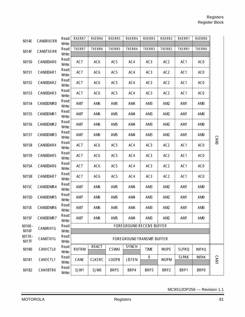
RegistersRegister Block
MC9S12DP256 — Revision 1.1
MOTOROLA Registers 81
$014E CAN0RXERRRead: RXERR7 RXERR6 RXERR5 RXERR4 RXERR3 RXERR2 RXERR1 RXERR0
CAN
0
Write:
$014F CAN0TXERRRead: TXERR7 TXERR6 TXERR5 TXERR4 TXERR3 TXERR2 TXERR1 TXERR0
Write:
$0150 CAN0IDAR0Read:
AC7 AC6 AC5 AC4 AC3 AC2 AC1 AC0Write:
$0151 CAN0IDAR1Read:
AC7 AC6 AC5 AC4 AC3 AC2 AC1 AC0Write:
$0152 CAN0IDAR2Read:
AC7 AC6 AC5 AC4 AC3 AC2 AC1 AC0Write:
$0153 CAN0IDAR3Read:
AC7 AC6 AC5 AC4 AC3 AC2 AC1 AC0Write:
$0154 CAN0IDMR0Read:
AM7 AM6 AM5 AM4 AM3 AM2 AM1 AM0Write:
$0155 CAN0IDMR1Read:
AM7 AM6 AM5 AM4 AM3 AM2 AM1 AM0Write:
$0156 CAN0IDMR2Read:
AM7 AM6 AM5 AM4 AM3 AM2 AM1 AM0Write:
$0157 CAN0IDMR3Read:
AM7 AM6 AM5 AM4 AM3 AM2 AM1 AM0Write:
$0158 CAN0IDAR4Read:
AC7 AC6 AC5 AC4 AC3 AC2 AC1 AC0Write:
$0159 CAN0IDAR5Read:
AC7 AC6 AC5 AC4 AC3 AC2 AC1 AC0Write:
$015A CAN0IDAR6Read:
AC7 AC6 AC5 AC4 AC3 AC2 AC1 AC0Write:
$015B CAN0IDAR7Read:
AC7 AC6 AC5 AC4 AC3 AC2 AC1 AC0Write:
$015C CAN0IDMR4Read:
AM7 AM6 AM5 AM4 AM3 AM2 AM1 AM0Write:
$015D CAN0IDMR5Read:
AM7 AM6 AM5 AM4 AM3 AM2 AM1 AM0Write:
$015E CAN0IDMR6Read:
AM7 AM6 AM5 AM4 AM3 AM2 AM1 AM0Write:
$015F CAN0IDMR7Read:
AM7 AM6 AM5 AM4 AM3 AM2 AM1 AM0Write:
$0160 - $016F
CAN0RXFGRead: FOREGROUND RECEIVE BUFFERWrite:
$0170 - $017F
CAN0TXFGRead:
FOREGROUND TRANSMIT BUFFERWrite:
$0180 CAN1CTL0Read:
RXFRMRXACT
CSWAISYNCH
TIME WUPE SLPRQ INITRQ
CAN
1
Write:
$0181 CAN1CTL1Read:
CANE CLKSRC LOOPB LISTEN0
WUPMSLPAK INITAK
Write:
$0182 CAN1BTR0Read:
SJW1 SJW0 BRP5 BRP4 BRP3 BRP2 BRP1 BRP0Write:

Registers
MC9S12DP256 — Revision 1.1
82 Registers MOTOROLA
$0183 CAN1BTR1Read:
SAMP TSEG22 TSEG21 TSEG20 TSEG13 TSEG12 TSEG11 TSEG10
CAN
1
Write:
$0184 CAN1RFLGRead:
WUPIF CSCIFRSTAT1 RSTAT0 TSTAT1 TSTAT0
OVRIF RXFWrite:
$0185 CAN1RIERRead:
WUPIE CSCIE RSTATE1 RSTATE0 TSTATE1 TSTATE0 OVRIE RXFIEWrite:
$0186 CAN1TFLGRead: 0 0 0 0 0
TXE2 TXE1 TXE0Write:
$0187 CAN1TIERRead: 0 0 0 0 0
TXEIE2 TXEIE1 TXEIE0Write:
$0188 CAN1TARQRead: 0 0 0 0 0
ABTRQ2 ABTRQ1 ABTRQ0Write:
$0189 CAN1TAAKRead: 0 0 0 0 0
ABTAK2 ABTAK1 ABTAK0Write:
$018A CAN1TBSELRead: 0 0 0 0 0
TX2 TX1 TX0Write:
$018B CAN1IDACRead: 0 0
IDAM1 IDAM00 IDHIT2 IDHIT1 IDHIT0
Write:
$018C ReservedRead: 0 0 0 0 0 0 0 0Write:
$018D ReservedRead: 0 0 0 0 0 0 0 0Write:
$018E CAN1RXERRRead: RXERR7 RXERR6 RXERR5 RXERR4 RXERR3 RXERR2 RXERR1 RXERR0
Write:
$018F CAN1TXERRRead: TXERR7 TXERR6 TXERR5 TXERR4 TXERR3 TXERR2 TXERR1 TXERR0
Write:
$0190 CAN1IDAR0Read:
AC7 AC6 AC5 AC4 AC3 AC2 AC1 AC0Write:
$0191 CAN1IDAR1Read:
AC7 AC6 AC5 AC4 AC3 AC2 AC1 AC0Write:
$0192 CAN1IDAR2Read:
AC7 AC6 AC5 AC4 AC3 AC2 AC1 AC0Write:
$0193 CAN1IDAR3Read:
AC7 AC6 AC5 AC4 AC3 AC2 AC1 AC0Write:
$0194 CAN1IDMR0Read:
AM7 AM6 AM5 AM4 AM3 AM2 AM1 AM0Write:
$0195 CAN1IDMR1Read:
AM7 AM6 AM5 AM4 AM3 AM2 AM1 AM0Write:
$0196 CAN1IDMR2Read:
AM7 AM6 AM5 AM4 AM3 AM2 AM1 AM0Write:
$0197 CAN1IDMR3Read:
AM7 AM6 AM5 AM4 AM3 AM2 AM1 AM0Write:
$0198 CAN1IDAR4Read:
AC7 AC6 AC5 AC4 AC3 AC2 AC1 AC0Write:
$0199 CAN1IDAR5Read:
AC7 AC6 AC5 AC4 AC3 AC2 AC1 AC0Write:
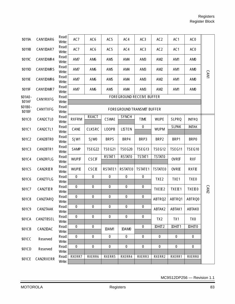
RegistersRegister Block
MC9S12DP256 — Revision 1.1
MOTOROLA Registers 83
$019A CAN1IDAR6Read:
AC7 AC6 AC5 AC4 AC3 AC2 AC1 AC0
CAN
1
Write:
$019B CAN1IDAR7Read:
AC7 AC6 AC5 AC4 AC3 AC2 AC1 AC0Write:
$019C CAN1IDMR4Read:
AM7 AM6 AM5 AM4 AM3 AM2 AM1 AM0Write:
$019D CAN1IDMR5Read:
AM7 AM6 AM5 AM4 AM3 AM2 AM1 AM0Write:
$019E CAN1IDMR6Read:
AM7 AM6 AM5 AM4 AM3 AM2 AM1 AM0Write:
$019F CAN1IDMR7Read:
AM7 AM6 AM5 AM4 AM3 AM2 AM1 AM0Write:
$01A0 - $01AF
CAN1RXFGRead: FOREGROUND RECEIVE BUFFERWrite:
$01B0 - $01BF
CAN1TXFGRead:
FOREGROUND TRANSMIT BUFFERWrite:
$01C0 CAN2CTL0Read:
RXFRMRXACT
CSWAISYNCH
TIME WUPE SLPRQ INITRQ
CAN
2
Write:
$01C1 CAN2CTL1Read:
CANE CLKSRC LOOPB LISTEN0
WUPMSLPAK INITAK
Write:
$01C2 CAN2BTR0Read:
SJW1 SJW0 BRP5 BRP4 BRP3 BRP2 BRP1 BRP0Write:
$01C3 CAN2BTR1Read:
SAMP TSEG22 TSEG21 TSEG20 TSEG13 TSEG12 TSEG11 TSEG10Write:
$01C4 CAN2RFLGRead:
WUPIF CSCIFRSTAT1 RSTAT0 TSTAT1 TSTAT0
OVRIF RXFWrite:
$01C5 CAN2RIERRead:
WUPIE CSCIE RSTATE1 RSTATE0 TSTATE1 TSTATE0 OVRIE RXFIEWrite:
$01C6 CAN2TFLGRead: 0 0 0 0 0
TXE2 TXE1 TXE0Write:
$01C7 CAN2TIERRead: 0 0 0 0 0
TXEIE2 TXEIE1 TXEIE0Write:
$01C8 CAN2TARQRead: 0 0 0 0 0
ABTRQ2 ABTRQ1 ABTRQ0Write:
$01C9 CAN2TAAKRead: 0 0 0 0 0
ABTAK2 ABTAK1 ABTAK0Write:
$01CA CAN2TBSELRead: 0 0 0 0 0
TX2 TX1 TX0Write:
$01CB CAN2IDACRead: 0 0
IDAM1 IDAM00 IDHIT2 IDHIT1 IDHIT0
Write:
$01CC ReservedRead: 0 0 0 0 0 0 0 0Write:
$01CD ReservedRead: 0 0 0 0 0 0 0 0Write:
$01CE CAN2RXERRRead: RXERR7 RXERR6 RXERR5 RXERR4 RXERR3 RXERR2 RXERR1 RXERR0
Write:
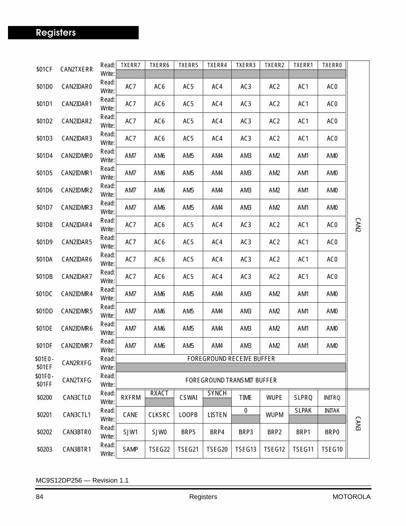
Registers
MC9S12DP256 — Revision 1.1
84 Registers MOTOROLA
$01CF CAN2TXERRRead: TXERR7 TXERR6 TXERR5 TXERR4 TXERR3 TXERR2 TXERR1 TXERR0
CAN
2
Write:
$01D0 CAN2IDAR0Read:
AC7 AC6 AC5 AC4 AC3 AC2 AC1 AC0Write:
$01D1 CAN2IDAR1Read:
AC7 AC6 AC5 AC4 AC3 AC2 AC1 AC0Write:
$01D2 CAN2IDAR2Read:
AC7 AC6 AC5 AC4 AC3 AC2 AC1 AC0Write:
$01D3 CAN2IDAR3Read:
AC7 AC6 AC5 AC4 AC3 AC2 AC1 AC0Write:
$01D4 CAN2IDMR0Read:
AM7 AM6 AM5 AM4 AM3 AM2 AM1 AM0Write:
$01D5 CAN2IDMR1Read:
AM7 AM6 AM5 AM4 AM3 AM2 AM1 AM0Write:
$01D6 CAN2IDMR2Read:
AM7 AM6 AM5 AM4 AM3 AM2 AM1 AM0Write:
$01D7 CAN2IDMR3Read:
AM7 AM6 AM5 AM4 AM3 AM2 AM1 AM0Write:
$01D8 CAN2IDAR4Read:
AC7 AC6 AC5 AC4 AC3 AC2 AC1 AC0Write:
$01D9 CAN2IDAR5Read:
AC7 AC6 AC5 AC4 AC3 AC2 AC1 AC0Write:
$01DA CAN2IDAR6Read:
AC7 AC6 AC5 AC4 AC3 AC2 AC1 AC0Write:
$01DB CAN2IDAR7Read:
AC7 AC6 AC5 AC4 AC3 AC2 AC1 AC0Write:
$01DC CAN2IDMR4Read:
AM7 AM6 AM5 AM4 AM3 AM2 AM1 AM0Write:
$01DD CAN2IDMR5Read:
AM7 AM6 AM5 AM4 AM3 AM2 AM1 AM0Write:
$01DE CAN2IDMR6Read:
AM7 AM6 AM5 AM4 AM3 AM2 AM1 AM0Write:
$01DF CAN2IDMR7Read:
AM7 AM6 AM5 AM4 AM3 AM2 AM1 AM0Write:
$01E0 - $01EF
CAN2RXFGRead: FOREGROUND RECEIVE BUFFERWrite:
$01F0 - $01FF
CAN2TXFGRead:
FOREGROUND TRANSMIT BUFFERWrite:
$0200 CAN3CTL0Read:
RXFRMRXACT
CSWAISYNCH
TIME WUPE SLPRQ INITRQ
CAN
3
Write:
$0201 CAN3CTL1Read:
CANE CLKSRC LOOPB LISTEN0
WUPMSLPAK INITAK
Write:
$0202 CAN3BTR0Read:
SJW1 SJW0 BRP5 BRP4 BRP3 BRP2 BRP1 BRP0Write:
$0203 CAN3BTR1Read:
SAMP TSEG22 TSEG21 TSEG20 TSEG13 TSEG12 TSEG11 TSEG10Write:

RegistersRegister Block
MC9S12DP256 — Revision 1.1
MOTOROLA Registers 85
$0204 CAN3RFLGRead:
WUPIF CSCIFRSTAT1 RSTAT0 TSTAT1 TSTAT0
OVRIF RXF
CAN
3
Write:
$0205 CAN3RIERRead:
WUPIE CSCIE RSTATE1 RSTATE0 TSTATE1 TSTATE0 OVRIE RXFIEWrite:
$0206 CAN3TFLGRead: 0 0 0 0 0
TXE2 TXE1 TXE0Write:
$0207 CAN3TIERRead: 0 0 0 0 0
TXEIE2 TXEIE1 TXEIE0Write:
$0208 CAN3TARQRead: 0 0 0 0 0
ABTRQ2 ABTRQ1 ABTRQ0Write:
$0209 CAN3TAAKRead: 0 0 0 0 0
ABTAK2 ABTAK1 ABTAK0Write:
$020A CAN3TBSELRead: 0 0 0 0 0
TX2 TX1 TX0Write:
$020B CAN3IDACRead: 0 0
IDAM1 IDAM00 IDHIT2 IDHIT1 IDHIT0
Write:
$020C ReservedRead: 0 0 0 0 0 0 0 0Write:
$020D ReservedRead: 0 0 0 0 0 0 0 0Write:
$020E CAN3RXERRRead: RXERR7 RXERR6 RXERR5 RXERR4 RXERR3 RXERR2 RXERR1 RXERR0
Write:
$020F CAN3TXERRRead: TXERR7 TXERR6 TXERR5 TXERR4 TXERR3 TXERR2 TXERR1 TXERR0
Write:
$0210 CAN3IDAR0Read:
AC7 AC6 AC5 AC4 AC3 AC2 AC1 AC0Write:
$0211 CAN3IDAR1Read:
AC7 AC6 AC5 AC4 AC3 AC2 AC1 AC0Write:
$0212 CAN3IDAR2Read:
AC7 AC6 AC5 AC4 AC3 AC2 AC1 AC0Write:
$0213 CAN3IDAR3Read:
AC7 AC6 AC5 AC4 AC3 AC2 AC1 AC0Write:
$0214 CAN3IDMR0Read:
AM7 AM6 AM5 AM4 AM3 AM2 AM1 AM0Write:
$0215 CAN3IDMR1Read:
AM7 AM6 AM5 AM4 AM3 AM2 AM1 AM0Write:
$0216 CAN3IDMR2Read:
AM7 AM6 AM5 AM4 AM3 AM2 AM1 AM0Write:
$0217 CAN3IDMR3Read:
AM7 AM6 AM5 AM4 AM3 AM2 AM1 AM0Write:
$0218 CAN3IDAR4Read:
AC7 AC6 AC5 AC4 AC3 AC2 AC1 AC0Write:
$0219 CAN3IDAR5Read:
AC7 AC6 AC5 AC4 AC3 AC2 AC1 AC0Write:
$021A CAN3IDAR6Read:
AC7 AC6 AC5 AC4 AC3 AC2 AC1 AC0Write:
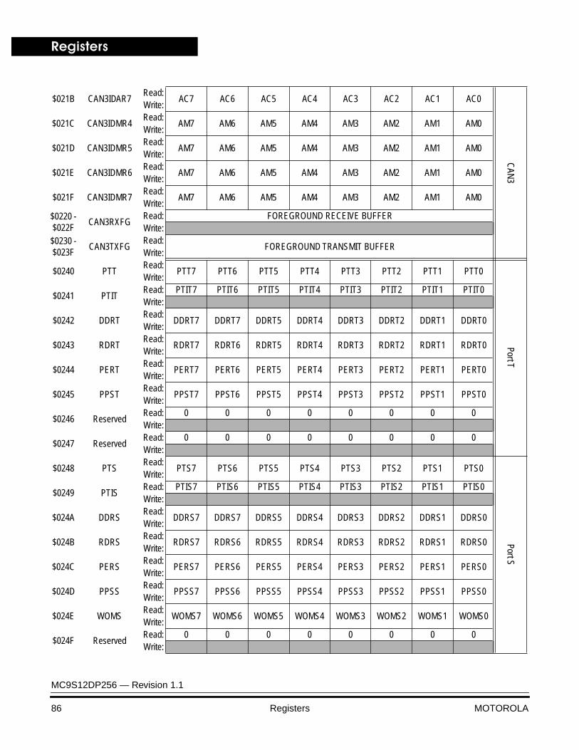
Registers
MC9S12DP256 — Revision 1.1
86 Registers MOTOROLA
$021B CAN3IDAR7Read:
AC7 AC6 AC5 AC4 AC3 AC2 AC1 AC0
CAN
3
Write:
$021C CAN3IDMR4Read:
AM7 AM6 AM5 AM4 AM3 AM2 AM1 AM0Write:
$021D CAN3IDMR5Read:
AM7 AM6 AM5 AM4 AM3 AM2 AM1 AM0Write:
$021E CAN3IDMR6Read:
AM7 AM6 AM5 AM4 AM3 AM2 AM1 AM0Write:
$021F CAN3IDMR7Read:
AM7 AM6 AM5 AM4 AM3 AM2 AM1 AM0Write:
$0220 - $022F
CAN3RXFGRead: FOREGROUND RECEIVE BUFFERWrite:
$0230 - $023F
CAN3TXFGRead:
FOREGROUND TRANSMIT BUFFERWrite:
$0240 PTTRead:
PTT7 PTT6 PTT5 PTT4 PTT3 PTT2 PTT1 PTT0
Port T
Write:
$0241 PTITRead: PTIT7 PTIT6 PTIT5 PTIT4 PTIT3 PTIT2 PTIT1 PTIT0Write:
$0242 DDRTRead:
DDRT7 DDRT7 DDRT5 DDRT4 DDRT3 DDRT2 DDRT1 DDRT0Write:
$0243 RDRTRead:
RDRT7 RDRT6 RDRT5 RDRT4 RDRT3 RDRT2 RDRT1 RDRT0Write:
$0244 PERTRead:
PERT7 PERT6 PERT5 PERT4 PERT3 PERT2 PERT1 PERT0Write:
$0245 PPSTRead:
PPST7 PPST6 PPST5 PPST4 PPST3 PPST2 PPST1 PPST0Write:
$0246 ReservedRead: 0 0 0 0 0 0 0 0Write:
$0247 ReservedRead: 0 0 0 0 0 0 0 0Write:
$0248 PTSRead:
PTS7 PTS6 PTS5 PTS4 PTS3 PTS2 PTS1 PTS0
Port S
Write:
$0249 PTISRead: PTIS7 PTIS6 PTIS5 PTIS4 PTIS3 PTIS2 PTIS1 PTIS0Write:
$024A DDRSRead:
DDRS7 DDRS7 DDRS5 DDRS4 DDRS3 DDRS2 DDRS1 DDRS0Write:
$024B RDRSRead:
RDRS7 RDRS6 RDRS5 RDRS4 RDRS3 RDRS2 RDRS1 RDRS0Write:
$024C PERSRead:
PERS7 PERS6 PERS5 PERS4 PERS3 PERS2 PERS1 PERS0Write:
$024D PPSSRead:
PPSS7 PPSS6 PPSS5 PPSS4 PPSS3 PPSS2 PPSS1 PPSS0Write:
$024E WOMSRead:
WOMS7 WOMS6 WOMS5 WOMS4 WOMS3 WOMS2 WOMS1 WOMS0Write:
$024F ReservedRead: 0 0 0 0 0 0 0 0Write:
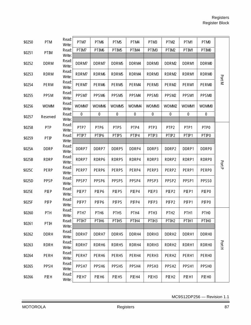
RegistersRegister Block
MC9S12DP256 — Revision 1.1
MOTOROLA Registers 87
$0250 PTMRead:
PTM7 PTM6 PTM5 PTM4 PTM3 PTM2 PTM1 PTM0
Port M
Write:
$0251 PTIMRead: PTIM7 PTIM6 PTIM5 PTIM4 PTIM3 PTIM2 PTIM1 PTIM0Write:
$0252 DDRMRead:
DDRM7 DDRM7 DDRM5 DDRM4 DDRM3 DDRM2 DDRM1 DDRM0Write:
$0253 RDRMRead:
RDRM7 RDRM6 RDRM5 RDRM4 RDRM3 RDRM2 RDRM1 RDRM0Write:
$0254 PERMRead:
PERM7 PERM6 PERM5 PERM4 PERM3 PERM2 PERM1 PERM0Write:
$0255 PPSMRead:
PPSM7 PPSM6 PPSM5 PPSM4 PPSM3 PPSM2 PPSM1 PPSM0Write:
$0256 WOMMRead:
WOMM7 WOMM6 WOMM5 WOMM4 WOMM3 WOMM2 WOMM1 WOMM0Write:
$0257 ReservedRead: 0 0 0 0 0 0 0 0Write:
$0258 PTPRead:
PTP7 PTP6 PTP5 PTP4 PTP3 PTP2 PTP1 PTP0
Port P
Write:
$0259 PTIPRead: PTIP7 PTIP6 PTIP5 PTIP4 PTIP3 PTIP2 PTIP1 PTIP0Write:
$025A DDRPRead:
DDRP7 DDRP7 DDRP5 DDRP4 DDRP3 DDRP2 DDRP1 DDRP0Write:
$025B RDRPRead:
RDRP7 RDRP6 RDRP5 RDRP4 RDRP3 RDRP2 RDRP1 RDRP0Write:
$025C PERPRead:
PERP7 PERP6 PERP5 PERP4 PERP3 PERP2 PERP1 PERP0Write:
$025D PPSPRead:
PPSP7 PPSP6 PPSP5 PPSP4 PPSP3 PPSP2 PPSP1 PPSS0Write:
$025E PIEPRead:
PIEP7 PIEP6 PIEP5 PIEP4 PIEP3 PIEP2 PIEP1 PIEP0Write:
$025F PIFPRead:
PIFP7 PIFP6 PIFP5 PIFP4 PIFP3 PIFP2 PIFP1 PIFP0Write:
$0260 PTHRead:
PTH7 PTH6 PTH5 PTH4 PTH3 PTH2 PTH1 PTH0
Port H
Write:
$0261 PTIHRead: PTIH7 PTIH6 PTIH5 PTIH4 PTIH3 PTIH2 PTIH1 PTIH0Write:
$0262 DDRHRead:
DDRH7 DDRH7 DDRH5 DDRH4 DDRH3 DDRH2 DDRH1 DDRH0Write:
$0263 RDRHRead:
RDRH7 RDRH6 RDRH5 RDRH4 RDRH3 RDRH2 RDRH1 RDRH0Write:
$0264 PERHRead:
PERH7 PERH6 PERH5 PERH4 PERH3 PERH2 PERH1 PERH0Write:
$0265 PPSHRead:
PPSH7 PPSH6 PPSH5 PPSH4 PPSH3 PPSH2 PPSH1 PPSH0Write:
$0266 PIEHRead:
PIEH7 PIEH6 PIEH5 PIEH4 PIEH3 PIEH2 PIEH1 PIEH0Write:
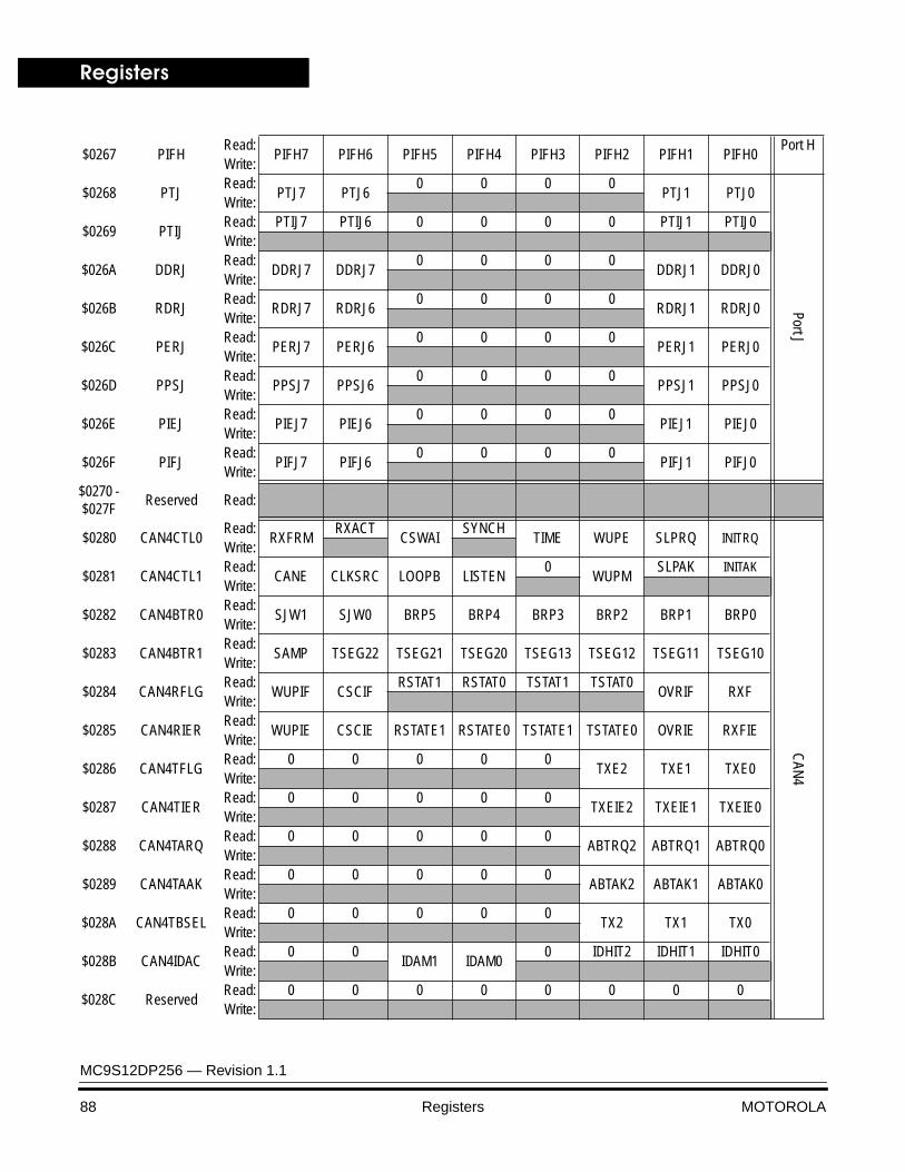
Registers
MC9S12DP256 — Revision 1.1
88 Registers MOTOROLA
$0267 PIFHRead:
PIFH7 PIFH6 PIFH5 PIFH4 PIFH3 PIFH2 PIFH1 PIFH0Port H
Write:
$0268 PTJRead:
PTJ7 PTJ60 0 0 0
PTJ1 PTJ0
Port J
Write:
$0269 PTIJRead: PTIJ7 PTIJ6 0 0 0 0 PTIJ1 PTIJ0Write:
$026A DDRJRead:
DDRJ7 DDRJ70 0 0 0
DDRJ1 DDRJ0Write:
$026B RDRJRead:
RDRJ7 RDRJ60 0 0 0
RDRJ1 RDRJ0Write:
$026C PERJRead:
PERJ7 PERJ60 0 0 0
PERJ1 PERJ0Write:
$026D PPSJRead:
PPSJ7 PPSJ60 0 0 0
PPSJ1 PPSJ0Write:
$026E PIEJRead:
PIEJ7 PIEJ60 0 0 0
PIEJ1 PIEJ0Write:
$026F PIFJRead:
PIFJ7 PIFJ60 0 0 0
PIFJ1 PIFJ0Write:
$0270 - $027F
Reserved Read:
$0280 CAN4CTL0Read:
RXFRMRXACT
CSWAISYNCH
TIME WUPE SLPRQ INITRQ
CAN
4
Write:
$0281 CAN4CTL1Read:
CANE CLKSRC LOOPB LISTEN0
WUPMSLPAK INITAK
Write:
$0282 CAN4BTR0Read:
SJW1 SJW0 BRP5 BRP4 BRP3 BRP2 BRP1 BRP0Write:
$0283 CAN4BTR1Read:
SAMP TSEG22 TSEG21 TSEG20 TSEG13 TSEG12 TSEG11 TSEG10Write:
$0284 CAN4RFLGRead:
WUPIF CSCIFRSTAT1 RSTAT0 TSTAT1 TSTAT0
OVRIF RXFWrite:
$0285 CAN4RIERRead:
WUPIE CSCIE RSTATE1 RSTATE0 TSTATE1 TSTATE0 OVRIE RXFIEWrite:
$0286 CAN4TFLGRead: 0 0 0 0 0
TXE2 TXE1 TXE0Write:
$0287 CAN4TIERRead: 0 0 0 0 0
TXEIE2 TXEIE1 TXEIE0Write:
$0288 CAN4TARQRead: 0 0 0 0 0
ABTRQ2 ABTRQ1 ABTRQ0Write:
$0289 CAN4TAAKRead: 0 0 0 0 0
ABTAK2 ABTAK1 ABTAK0Write:
$028A CAN4TBSELRead: 0 0 0 0 0
TX2 TX1 TX0Write:
$028B CAN4IDACRead: 0 0
IDAM1 IDAM00 IDHIT2 IDHIT1 IDHIT0
Write:
$028C ReservedRead: 0 0 0 0 0 0 0 0Write:
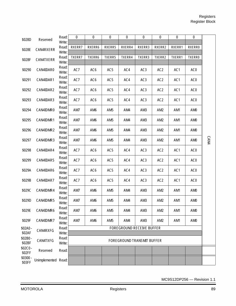
RegistersRegister Block
MC9S12DP256 — Revision 1.1
MOTOROLA Registers 89
$028D ReservedRead: 0 0 0 0 0 0 0 0
CAN
4
Write:
$028E CAN4RXERRRead: RXERR7 RXERR6 RXERR5 RXERR4 RXERR3 RXERR2 RXERR1 RXERR0
Write:
$028F CAN4TXERRRead: TXERR7 TXERR6 TXERR5 TXERR4 TXERR3 TXERR2 TXERR1 TXERR0
Write:
$0290 CAN4IDAR0Read:
AC7 AC6 AC5 AC4 AC3 AC2 AC1 AC0Write:
$0291 CAN4IDAR1Read:
AC7 AC6 AC5 AC4 AC3 AC2 AC1 AC0Write:
$0292 CAN4IDAR2Read:
AC7 AC6 AC5 AC4 AC3 AC2 AC1 AC0Write:
$0293 CAN4IDAR3Read:
AC7 AC6 AC5 AC4 AC3 AC2 AC1 AC0Write:
$0294 CAN4IDMR0Read:
AM7 AM6 AM5 AM4 AM3 AM2 AM1 AM0Write:
$0295 CAN4IDMR1Read:
AM7 AM6 AM5 AM4 AM3 AM2 AM1 AM0Write:
$0296 CAN4IDMR2Read:
AM7 AM6 AM5 AM4 AM3 AM2 AM1 AM0Write:
$0297 CAN4IDMR3Read:
AM7 AM6 AM5 AM4 AM3 AM2 AM1 AM0Write:
$0298 CAN4IDAR4Read:
AC7 AC6 AC5 AC4 AC3 AC2 AC1 AC0Write:
$0299 CAN4IDAR5Read:
AC7 AC6 AC5 AC4 AC3 AC2 AC1 AC0Write:
$029A CAN4IDAR6Read:
AC7 AC6 AC5 AC4 AC3 AC2 AC1 AC0Write:
$029B CAN4IDAR7Read:
AC7 AC6 AC5 AC4 AC3 AC2 AC1 AC0Write:
$029C CAN4IDMR4Read:
AM7 AM6 AM5 AM4 AM3 AM2 AM1 AM0Write:
$029D CAN4IDMR5Read:
AM7 AM6 AM5 AM4 AM3 AM2 AM1 AM0Write:
$029E CAN4IDMR6Read:
AM7 AM6 AM5 AM4 AM3 AM2 AM1 AM0Write:
$029F CAN4IDMR7Read:
AM7 AM6 AM5 AM4 AM3 AM2 AM1 AM0Write:
$02A0 - $02AF
CAN4RXFGRead: FOREGROUND RECEIVE BUFFERWrite:
$02B0 - $02BF
CAN4TXFGRead:
FOREGROUND TRANSMIT BUFFERWrite:
$02C0 - $02FF
Reserved Read:
$0300 - $03FF
Unimplemented Read:

Registers
MC9S12DP256 — Revision 1.1
90 Registers MOTOROLA
MC9S12DP256 — Revision 1.1
MOTOROLA Operating Modes 91
Operating ModesOperating Modes
Contents
Introduction . . . . . . . . . . . . . . . . . . . . . . . . . . . . . . . . . . . . . . . . . . . . . 91Operating Modes. . . . . . . . . . . . . . . . . . . . . . . . . . . . . . . . . . . . . . . . . 91Background Debug Mode . . . . . . . . . . . . . . . . . . . . . . . . . . . . . . . . . 102Security . . . . . . . . . . . . . . . . . . . . . . . . . . . . . . . . . . . . . . . . . . . . . . . 103
Introduction
Eight possible operating modes determine the operating configuration of the MC9S12DP256. Each mode has an associated default memory map and external bus configuration.
Operating Modes
The operating mode out of reset is determined by the states of the MODC, MODB, and MODA pins during reset.
The MODC, MODB, and MODA bits in the MODE register show current operating mode and provide limited mode switching during operation. The states of the MODC, MODB, and MODA pins are latched into these bits on the rising edge of the reset signal.
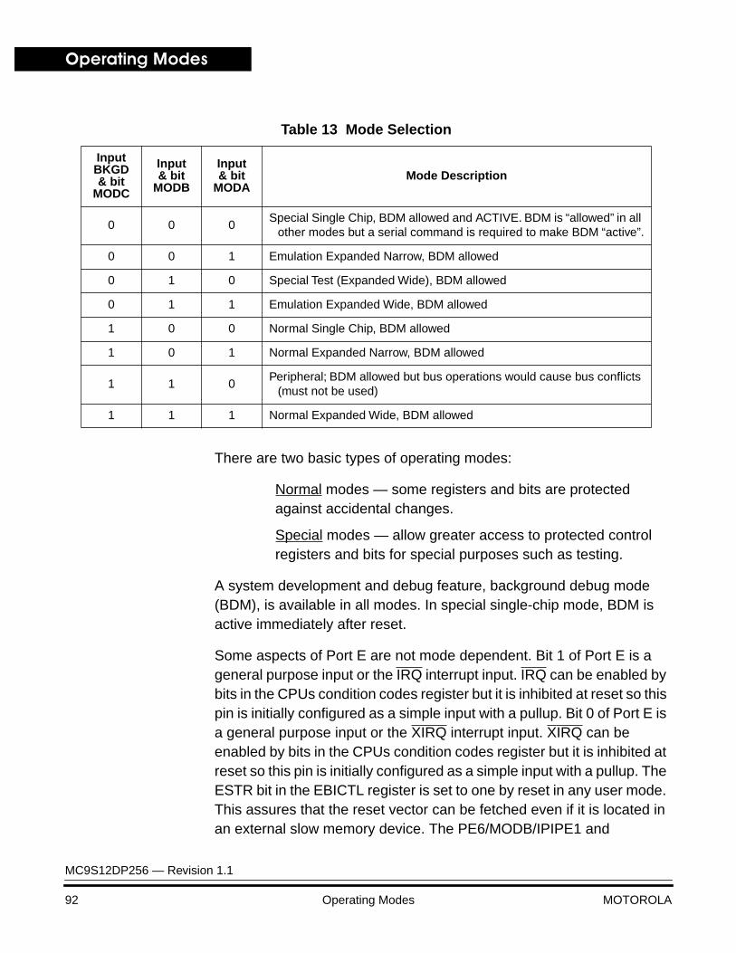
Operating Modes
MC9S12DP256 — Revision 1.1
92 Operating Modes MOTOROLA
There are two basic types of operating modes:
Normal modes — some registers and bits are protected against accidental changes.
Special modes — allow greater access to protected control registers and bits for special purposes such as testing.
A system development and debug feature, background debug mode (BDM), is available in all modes. In special single-chip mode, BDM is active immediately after reset.
Some aspects of Port E are not mode dependent. Bit 1 of Port E is a general purpose input or the IRQ interrupt input. IRQ can be enabled by bits in the CPUs condition codes register but it is inhibited at reset so this pin is initially configured as a simple input with a pullup. Bit 0 of Port E is a general purpose input or the XIRQ interrupt input. XIRQ can be enabled by bits in the CPUs condition codes register but it is inhibited at reset so this pin is initially configured as a simple input with a pullup. The ESTR bit in the EBICTL register is set to one by reset in any user mode. This assures that the reset vector can be fetched even if it is located in an external slow memory device. The PE6/MODB/IPIPE1 and
Table 13 Mode Selection
Input BKGD& bit
MODC
Input & bit
MODB
Input & bit
MODAMode Description
0 0 0Special Single Chip, BDM allowed and ACTIVE. BDM is “allowed” in all
other modes but a serial command is required to make BDM “active”.
0 0 1 Emulation Expanded Narrow, BDM allowed
0 1 0 Special Test (Expanded Wide), BDM allowed
0 1 1 Emulation Expanded Wide, BDM allowed
1 0 0 Normal Single Chip, BDM allowed
1 0 1 Normal Expanded Narrow, BDM allowed
1 1 0Peripheral; BDM allowed but bus operations would cause bus conflicts
(must not be used)
1 1 1 Normal Expanded Wide, BDM allowed
Operating ModesOperating Modes
MC9S12DP256 — Revision 1.1
MOTOROLA Operating Modes 93
PE5/MODA/IPIPE0 pins act as high-impedance mode select inputs during reset.
The following paragraphs discuss the default bus setup and describe which aspects of the bus can be changed after reset on a per mode basis.
Normal Operating Modes
These modes provide three operating configurations. Background debug is available in all three modes, but must first be enabled for some operations by means of a BDM background command, then activated.
Normal Single-Chip Mode — There is no external expansion bus in this mode. All pins of Ports A, B and E are configured as general purpose I/O pins Port E bits 1 and 0 are available as general purpose input only pins with internal pullups enabled. All other pins of Port E are bidirectional I/O pins that are initially configured as high-impedance inputs with internal pullups enabled. Ports A and B are configured as high-impedance inputs with their internal pullups disabled.
The pins associated with Port E bits 6, 5, 3, and 2 cannot be configured for their alternate functions IPIPE1, IPIPE0, LSTRB, and R/W while the MCU is in single chip modes. In single chip modes, the associated control bits PIPOE, LSTRE, and RDWE are reset to zero. Writing the opposite state into them in single chip mode does not change the operation of the associated Port E pins.
In normal single chip mode, the MODE register is writable one time. This allows a user program to change the bus mode to special single chip or narrow or wide expanded mode and/or turn on visibility of internal accesses.
Port E, bit 4 can be configured for a free-running E clock output by clearing NECLK=0. Typically the only use for an E clock output while the MCU is in single chip modes would be to get a constant speed clock for use in the external application system.
Operating Modes
MC9S12DP256 — Revision 1.1
94 Operating Modes MOTOROLA
Normal Expanded Wide Mode — In expanded wide modes, Ports A and B are configured as a 16-bit multiplexed address and data bus and Port E bit 4 is configured as the E clock output signal. These signals allow external memory and peripheral devices to be interfaced to the MCU.
Port E pins other than PE4/ECLK are configured as general purpose I/O pins (initially high-impedance inputs with internal pullup resistors enabled). Control bits PIPOE, NECLK, LSTRE, and RDWE in the PEAR register can be used to configure Port E pins to act as bus control outputs instead of general purpose I/O pins.
It is possible to enable the pipe status signals on Port E bits 6 and 5 by setting the PIPOE bit in PEAR, but it would be unusual to do so in this mode. Development systems where pipe status signals are monitored would typically use the special variation of this mode.
The Port E bit 2 pin can be reconfigured as the R/W bus control signal by writing “1” to the RDWE bit in PEAR. If the expanded system includes external devices that can be written, such as RAM, the RDWE bit would need to be set before any attempt to write to an external location. If there are no writable resources in the external system, PE2 can be left as a general purpose I/O pin.
The Port E bit 3 pin can be reconfigured as the LSTRB bus control signal by writing “1” to the LSTRE bit in PEAR. The default condition of this pin is a general purpose input because the LSTRB function is not needed in all expanded wide applications.
The Port E bit 4 pin is initially configured as ECLK output with stretch. The E clock output function depends upon the settings of the NECLK bit in the PEAR register, the IVIS bit in the MODE register and the ESTR bit in the EBICTL register. The E clock is available for use in external select decode logic or as a constant speed clock for use in the external application system.
Operating ModesOperating Modes
MC9S12DP256 — Revision 1.1
MOTOROLA Operating Modes 95
Normal Expanded Narrow Mode — This mode is used for lower cost production systems that use 8-bit wide external EPROMs or RAMs. Such systems take extra bus cycles to access 16-bit locations but this may be preferred over the extra cost of additional external memory devices.
Ports A and B are configured as a 16-bit address bus and Port A is multiplexed with data. Internal visibility is not available in this mode because the internal cycles would need to be split into two 8-bit cycles.
Since the PEAR register can only be written one time in this mode, use care to set all bits to the desired states during the single allowed write.
The PE3/LSTRB pin is always a general purpose I/O pin in normal expanded narrow mode. Although it is possible to write the LSTRE bit in PEAR to “1” in this mode, the state of LSTRE is overridden and Port E bit 3 cannot be reconfigured as the LSTRB output.
It is possible to enable the pipe status signals on Port E bits 6 and 5 by setting the PIPOE bit in PEAR, but it would be unusual to do so in this mode. LSTRB would also be needed to fully understand system activity. Development systems where pipe status signals are monitored would typically use special expanded wide mode or occasionally special expanded narrow mode.
The PE4/ECLK pin is initially configured as ECLK output with stretch. The E clock output function depends upon the settings of the NECLK bit in the PEAR register, the IVIS bit in the MODE register and the ESTR bit in the EBICTL register. In normal expanded narrow mode, the E clock is available for use in external select decode logic or as a constant speed clock for use in the external application system.
The PE2/R/W pin is initially configured as a general purpose input with a pullup but this pin can be reconfigured as the R/W bus control signal by writing “1” to the RDWE bit in PEAR. If the expanded narrow system includes external devices that can be written such as RAM, the RDWE bit would need to be set before
Operating Modes
MC9S12DP256 — Revision 1.1
96 Operating Modes MOTOROLA
any attempt to write to an external location. If there are no writable resources in the external system, PE2 can be left as a general purpose I/O pin.
Internal Visibility — Internal visibility is available when the MCU is operating in expanded wide modes or special narrow mode. It is not available in single-chip, peripheral or normal expanded narrow modes. Internal visibility is enabled by setting the IVIS bit in the MODE register.
If an internal access is made while E, R/W, and LSTRB are configured as bus control outputs and internal visibility is off (IVIS=0), E will remain low for the cycle, R/W will remain high, and address, data and the LSTRB pins will remain at their previous state.
When internal visibility is enabled (IVIS=1), certain internal cycles will be blocked from going external. During cycles when the BDM is selected, R/W will remain high, data will maintain its previous state, and address and LSTRB pins will be updated with the internal value. During CPU no access cycles when the BDM is not driving, R/W will remain high, and address, data and the LSTRB pins will remain at their previous state.
Emulation Expanded Wide Mode — In expanded wide modes, Ports A and B are configured as a 16-bit multiplexed address and data bus and Port E provides bus control and status signals. These signals allow external memory and peripheral devices to be interfaced to the MCU. These signals can also be used by a logic analyzer to monitor the progress of application programs.
The bus control related pins in Port E (PE7/NOACC, PE6/MODB/IPIPE1, PE5/MODA/IPIPE0, PE4/ECLK, PE3/LSTRB/TAGLO, and PE2/R/W) are all configured to serve their bus control output functions rather than general purpose I/O. Notice that writes to the bus control enable bits in the PEAR register in special mode are restricted.
The main difference between special modes and normal modes is that some of the bus control and system control signals cannot be written in special modes.

Operating ModesOperating Modes
MC9S12DP256 — Revision 1.1
MOTOROLA Operating Modes 97
Emulation Expanded Narrow Mode — Expanded narrow modes are intended to allow connection of single 8-bit external memory devices for lower cost systems that do not need the performance of a full 16-bit external data bus. Accesses to internal resources that have been mapped external (i.e. PORTA, PORTB, DDRA, DDRB, PORTE, DDRE, PEAR, PUCR, RDRIV) will be accessed with a 16-bit data bus on Ports A and B. Accesses of 16-bit external words to addresses which are normally mapped external will be broken into two separate 8-bit accesses using Port A as an 8-bit data bus. Internal operations continue to use full 16-bit data paths. They are only visible externally as 16-bit information if IVIS=1.
Ports A and B are configured as multiplexed address and data output ports. During external accesses, address A15, data D15 and D7 are associated with PA7, address A0 is associated with PB0 and data D8 and D0 are associated with PA0. During internal visible accesses and accesses to internal resources that have been mapped external, address A15 and data D15 is associated with PA7 and address A0 and data D0 is associated with PB0.
The bus control related pins in Port E (PE7/NOACC, PE6/MODB/IPIPE1, PE5/MODA/IPIPE0, PE4/ECLK, PE3/LSTRB/TAGLO, and PE2/R/W) are all configured to serve their bus control output functions rather than general purpose I/O. Notice that writes to the bus control enable bits in the PEAR register in special mode are restricted.
The main difference between special modes and normal modes is that some of the bus control and system control signals cannot be written in special modes.
Operating Modes
MC9S12DP256 — Revision 1.1
98 Operating Modes MOTOROLA
Special Operating Modes
There are two special operating modes that correspond to normal operating modes. These operating modes are commonly used in factory testing and system development.
Special Single-Chip Mode — When the MCU is reset in this mode, the background debug mode is enabled and “active”. The MCU does not fetch the reset vector and execute application code as it would in other modes. Instead the active background mode is in control of CPU execution and BDM firmware is waiting for additional serial commands through the BKGD pin. When a serial command instructs the MCU to return to normal execution, the system will be configured as described below unless the reset states of internal control registers have been changed through background commands after the MCU was reset.
There is no external expansion bus after reset in this mode. Ports A and B are initially simple bidirectional I/O pins that are configured as high-impedance inputs with internal pullups disabled; however, writing to the mode select bits in the MODE register (which is allowed in special modes) can change this after reset. All of the Port E pins (except PE4/ECLK) are initially configured as general purpose high-impedance inputs with pullups enabled. PE4/ECLK is configured as the E clock output in this mode.
The pins associated with Port E bits 6, 5, 3, and 2 cannot be configured for their alternate functions IPIPE1, IPIPE0, LSTRB, and R/W while the MCU is in single chip modes. In single chip modes, the associated control bits PIPOE, LSTRE and RDWE are reset to zero. Writing the opposite value into these bits in single chip mode does not change the operation of the associated Port E pins.
Port E, bit 4 can be configured for a free-running E clock output by clearing NECLK=0. Typically the only use for an E clock output while the MCU is in single chip modes would be to get a constant speed clock for use in the external application system.

Operating ModesOperating Modes
MC9S12DP256 — Revision 1.1
MOTOROLA Operating Modes 99
Special Test Mode — In expanded wide modes, Ports A and B are configured as a 16-bit multiplexed address and data bus and Port E provides bus control and status signals. In special test mode, the write protection of many control bits is lifted so that they can be thoroughly tested without needing to go through reset.
Test Operating Mode
There is a test operating mode in which an external master, such as an I.C. tester, can control the on-chip peripherals.
Peripheral Mode — This mode is intended for Motorola factory testing of the MCU. In this mode, the CPU is inactive and an external (tester) bus master drives address, data and bus control signals in through Ports A, B and E. In effect, the whole MCU acts as if it was a peripheral under control of an external CPU. This allows faster testing of on-chip memory and peripherals than previous testing methods. Since the mode control register is not accessible in peripheral mode, the only way to change to another mode is to reset the MCU into a different mode. Background debugging should not be used while the MCU is in special peripheral mode as internal bus conflicts between BDM and the external master can cause improper operation of both functions.
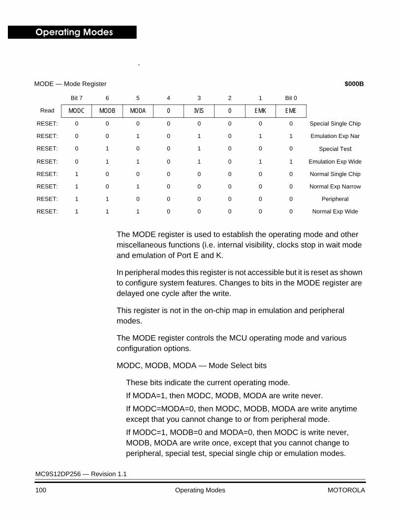
Operating Modes
MC9S12DP256 — Revision 1.1
100 Operating Modes MOTOROLA
.
The MODE register is used to establish the operating mode and other miscellaneous functions (i.e. internal visibility, clocks stop in wait mode and emulation of Port E and K.
In peripheral modes this register is not accessible but it is reset as shown to configure system features. Changes to bits in the MODE register are delayed one cycle after the write.
This register is not in the on-chip map in emulation and peripheral modes.
The MODE register controls the MCU operating mode and various configuration options.
MODC, MODB, MODA — Mode Select bits
These bits indicate the current operating mode.
If MODA=1, then MODC, MODB, MODA are write never.
If MODC=MODA=0, then MODC, MODB, MODA are write anytime except that you cannot change to or from peripheral mode.
If MODC=1, MODB=0 and MODA=0, then MODC is write never, MODB, MODA are write once, except that you cannot change to peripheral, special test, special single chip or emulation modes.
MODE — Mode Register $000B
Bit 7 6 5 4 3 2 1 Bit 0
Read MODC MODB MODA 0 IVIS 0 EMK EME
RESET: 0 0 0 0 0 0 0 0 Special Single Chip
RESET: 0 0 1 0 1 0 1 1 Emulation Exp Nar
RESET: 0 1 0 0 1 0 0 0 Special Test
RESET: 0 1 1 0 1 0 1 1 Emulation Exp Wide
RESET: 1 0 0 0 0 0 0 0 Normal Single Chip
RESET: 1 0 1 0 0 0 0 0 Normal Exp Narrow
RESET: 1 1 0 0 0 0 0 0 Peripheral
RESET: 1 1 1 0 0 0 0 0 Normal Exp Wide
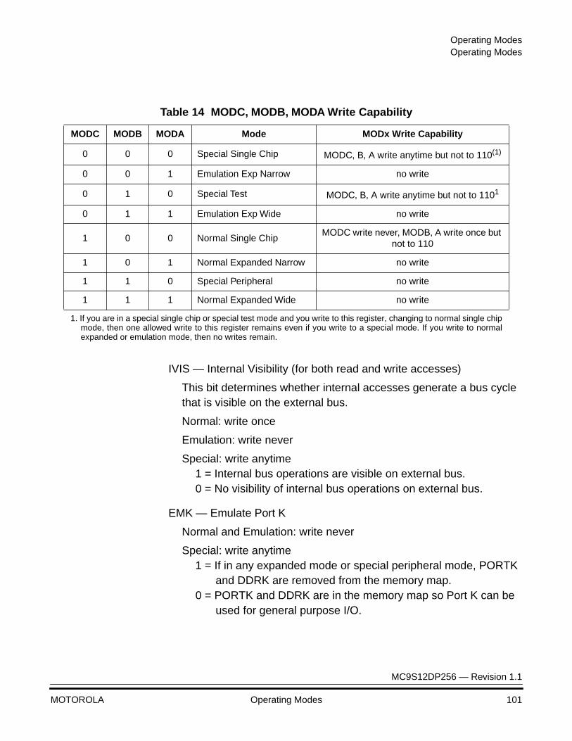
Operating ModesOperating Modes
MC9S12DP256 — Revision 1.1
MOTOROLA Operating Modes 101
IVIS — Internal Visibility (for both read and write accesses)
This bit determines whether internal accesses generate a bus cycle that is visible on the external bus.
Normal: write once
Emulation: write never
Special: write anytime1 = Internal bus operations are visible on external bus.0 = No visibility of internal bus operations on external bus.
EMK — Emulate Port K
Normal and Emulation: write never
Special: write anytime1 = If in any expanded mode or special peripheral mode, PORTK
and DDRK are removed from the memory map.0 = PORTK and DDRK are in the memory map so Port K can be
used for general purpose I/O.
Table 14 MODC, MODB, MODA Write Capability
MODC MODB MODA Mode MODx Write Capability
0 0 0 Special Single Chip MODC, B, A write anytime but not to 110(1)
0 0 1 Emulation Exp Narrow no write
0 1 0 Special Test MODC, B, A write anytime but not to 1101
0 1 1 Emulation Exp Wide no write
1 0 0 Normal Single Chip MODC write never, MODB, A write once but
not to 110
1 0 1 Normal Expanded Narrow no write
1 1 0 Special Peripheral no write
1 1 1 Normal Expanded Wide no write
1. If you are in a special single chip or special test mode and you write to this register, changing to normal single chipmode, then one allowed write to this register remains even if you write to a special mode. If you write to normalexpanded or emulation mode, then no writes remain.
Operating Modes
MC9S12DP256 — Revision 1.1
102 Operating Modes MOTOROLA
EME — Emulate Port E
Normal and Emulation: write never
Special: write anytime1 = If in any expanded mode or special peripheral mode, PORTE
and DDRE are removed from the memory map. Removing the registers from the map allows the user to emulate the function of these registers externally.
0 = PORTE and DDRE are in the memory map so Port E can be used for general purpose I/O.
In single-chip modes, PORTE and DDRE are always in the map regardless of the state of this bit.
Background Debug Mode
Background debug mode (BDM) is an auxiliary operating mode that is used for system development. BDM is implemented in on-chip hardware and provides a full set of debug operations. Some BDM commands can be executed while the CPU is operating normally. Other BDM commands are firmware based, and require the BDM firmware to be enabled and active for execution.
In special single-chip mode, BDM is enabled and active immediately out of reset. BDM is available in all other operating modes, but must be enabled before it can be activated. BDM should not be used in special peripheral mode because of potential bus conflicts.
Once enabled, background mode can be made active by a serial command sent via the BKGD pin or execution of a CPU12 BGND instruction. While background mode is active, the CPU can interpret special debugging commands, and read and write CPU registers, peripheral registers, and locations in memory.
While BDM is active, the CPU executes code located in a small on-chip ROM mapped to addresses $FF20 to $FFFF, and BDM control registers are accessible at addresses $FF00 to $FF06. The BDM ROM replaces the regular system vectors while BDM is active. While BDM is active, the

Operating ModesSecurity
MC9S12DP256 — Revision 1.1
MOTOROLA Operating Modes 103
user memory from $FF00 to $FFFF is not in the map except through serial BDM commands.
Security
The device will make available a security feature preventing the unauthorized read and write of the memory contents. This feature allows:
• Protection of the contents of FLASH,
• Protection of the contents of EEPROM,
• Operation in single-chip mode,
• Operation from external memory with internal FLASH and EEPROM disabled.
The user must be reminded that part of the security must lie with the user’s code. An extreme example would be user’s code that dumps the contents of the internal program. This code would defeat the purpose of security.
At the same time the user may also wish to put a “back door” in the user’s program. An example of this is the user downloads a “key” through the SCI which allows access to a programming routine that updates parameters stored in EEPROM.
Operation
Securing the Microcontroller
Once the user has programmed the FLASH and EEPROM (if desired), the part can be secured by programming the security bits located in the FLASH module. These non-volatile bits will keep the part secured through resetting the part and through powering down the part.
The security byte resides in a portion of the Flash array.
Two bits are used for security. The state of the security bits and the resulting state of security are shown in Table 15. Note that there are three secured bit combinations and only one unsecured combination.
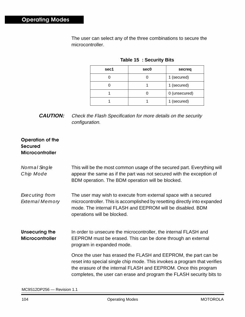
Operating Modes
MC9S12DP256 — Revision 1.1
104 Operating Modes MOTOROLA
The user can select any of the three combinations to secure the microcontroller.
CAUTION: Check the Flash Specification for more details on the security configuration.
Operation of the Secured Microcontroller
Normal Single Chip Mode
This will be the most common usage of the secured part. Everything will appear the same as if the part was not secured with the exception of BDM operation. The BDM operation will be blocked.
Executing from External Memory
The user may wish to execute from external space with a secured microcontroller. This is accomplished by resetting directly into expanded mode. The internal FLASH and EEPROM will be disabled. BDM operations will be blocked.
Unsecuring the Microcontroller
In order to unsecure the microcontroller, the internal FLASH and EEPROM must be erased. This can be done through an external program in expanded mode.
Once the user has erased the FLASH and EEPROM, the part can be reset into special single chip mode. This invokes a program that verifies the erasure of the internal FLASH and EEPROM. Once this program completes, the user can erase and program the FLASH security bits to
Table 15 : Security Bits
sec1 sec0 secreq
0 0 1 (secured)
0 1 1 (secured)
1 0 0 (unsecured)
1 1 1 (secured)
Operating ModesSecurity
MC9S12DP256 — Revision 1.1
MOTOROLA Operating Modes 105
the unsecured state. This is generally done through the BDM, but the user could also change to expanded mode (by writing the mode bits through the BDM) and jumping to an external program (again through BDM commands). Note that if the part goes through a reset before the security bits are reprogrammed to the unsecure state, the part will be secured again.

Operating Modes
MC9S12DP256 — Revision 1.1
106 Operating Modes MOTOROLA
MC9S12DP256 — Revision 1.1
MOTOROLA Resource Mapping 107
Resource MappingResource Mapping
Contents
Introduction . . . . . . . . . . . . . . . . . . . . . . . . . . . . . . . . . . . . . . . . . . . . 107Internal Resource Mapping . . . . . . . . . . . . . . . . . . . . . . . . . . . . . . . . 107Flash EEPROM mapping through internal Memory Expansion . . . . 111Miscellaneous System Control Register . . . . . . . . . . . . . . . . . . . . . . 118Memory Maps . . . . . . . . . . . . . . . . . . . . . . . . . . . . . . . . . . . . . . . . . . 119
Introduction
After reset, most system resources can be mapped to other addresses by writing to the appropriate control registers.
Internal Resource Mapping
The internal register block, RAM, and EEPROM have default locations within the 64K byte standard address space but may be reassigned to other locations during program execution by setting bits in mapping registers INITRG, INITRM, and INITEE. During normal operating modes these registers can be written once. It is advisable to explicitly establish these resource locations during the initialization phase of program execution, even if default values are chosen, in order to protect the registers from inadvertent modification later.
Writes to the mapping registers go into effect between the cycle that follows the write and the cycle after that. To assure that there are no unintended operations, a write to one of these registers should be followed with a NOP instruction.
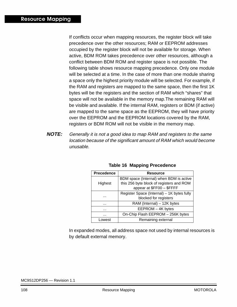
Resource Mapping
MC9S12DP256 — Revision 1.1
108 Resource Mapping MOTOROLA
If conflicts occur when mapping resources, the register block will take precedence over the other resources; RAM or EEPROM addresses occupied by the register block will not be available for storage. When active, BDM ROM takes precedence over other resources, although a conflict between BDM ROM and register space is not possible. The following table shows resource mapping precedence. Only one module will be selected at a time. In the case of more than one module sharing a space only the highest priority module will be selected. For example, if the RAM and registers are mapped to the same space, then the first 1K bytes will be the registers and the section of RAM which “shares” that space will not be available in the memory map.The remaining RAM will be visible and available. If the internal RAM, registers or BDM (if active) are mapped to the same space as the EEPROM, they will have priority over the EEPROM and the EEPROM locations covered by the RAM, registers or BDM ROM will not be visible in the memory map.
NOTE: Generally it is not a good idea to map RAM and registers to the same location because of the significant amount of RAM which would become unusable.
In expanded modes, all address space not used by internal resources is by default external memory.
Table 16 Mapping Precedence
Precedence Resource
HighestBDM space (Internal) when BDM is active this 256 byte block of registers and ROM
appear at $FF00 – $FFFF
...Register Space (Internal) – 1K bytes fully
blocked for registers... RAM (Internal) – 12K bytes... EEPROM – 4K bytes... On-Chip Flash EEPROM – 256K bytes
Lowest Remaining external

Resource MappingInternal Resource Mapping
MC9S12DP256 — Revision 1.1
MOTOROLA Resource Mapping 109
Register Block Mapping
After reset the 1K byte register block resides at location $0000 but can be reassigned to any 2K byte boundary within the first 32K byte of the 64K byte address space. Mapping of internal registers is controlled by five bits in the INITRG register. This register initializes the internal Registers position.
Normal and Emulation: Write once.
Special: Write anytime
Writes to this register take one cycle to go into effect.
Read: Anytime.
Reset to $00 (Registers located from $0000 to $03FF).
REG[15:11] — Internal register map position
These five bits specify the upper five bits of the register block’s address. INITRG Bit 7 is always set to “0”.
RAM Mapping The MC9S12DP256 has 12K bytes of fully static RAM that is used for storing instructions, variables, and temporary data during program execution. After reset, RAM addressing begins at location $1000 but can be assigned to any 16K byte boundary within the standard 64K byte address space. It occupies either the first 12K of the 16K space (i.e. $0000 – $2FFF, $4000 – $6FFF, etc.) or the last 12K of the 16K space (i.e. $1000 – $3FFF, $5000 – $7FFF, etc.). Mapping of internal RAM is controlled by three bits in the INITRM register.
Normal and Emulation: Write once.
Special: Write anytime.
NOTE: Writes to this register take one cycle to go into effect.
INITRG — Initialization of Internal Register Position Register
Address Offset: $0011
Bit 7 6 5 4 3 2 1 Bit 0
0 REG14 REG13 REG12 REG11 0 0 0
Reset: 0 0 0 0 0 0 0 0
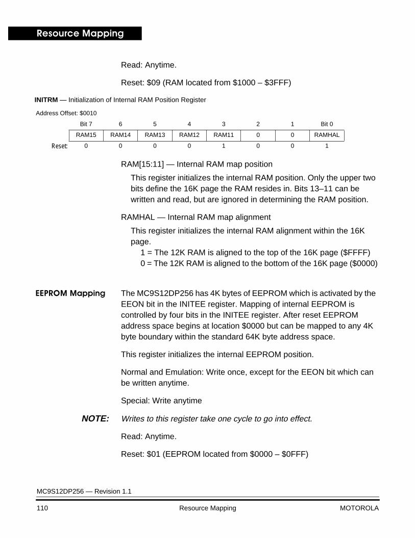
Resource Mapping
MC9S12DP256 — Revision 1.1
110 Resource Mapping MOTOROLA
Read: Anytime.
Reset: $09 (RAM located from $1000 – $3FFF)
RAM[15:11] — Internal RAM map position
This register initializes the internal RAM position. Only the upper two bits define the 16K page the RAM resides in. Bits 13–11 can be written and read, but are ignored in determining the RAM position.
RAMHAL — Internal RAM map alignment
This register initializes the internal RAM alignment within the 16K page.
1 = The 12K RAM is aligned to the top of the 16K page ($FFFF)0 = The 12K RAM is aligned to the bottom of the 16K page ($0000)
EEPROM Mapping The MC9S12DP256 has 4K bytes of EEPROM which is activated by the EEON bit in the INITEE register. Mapping of internal EEPROM is controlled by four bits in the INITEE register. After reset EEPROM address space begins at location $0000 but can be mapped to any 4K byte boundary within the standard 64K byte address space.
This register initializes the internal EEPROM position.
Normal and Emulation: Write once, except for the EEON bit which can be written anytime.
Special: Write anytime
NOTE: Writes to this register take one cycle to go into effect.
Read: Anytime.
Reset: $01 (EEPROM located from $0000 – $0FFF)
INITRM — Initialization of Internal RAM Position Register
Address Offset: $0010
Bit 7 6 5 4 3 2 1 Bit 0
RAM15 RAM14 RAM13 RAM12 RAM11 0 0 RAMHAL
Reset: 0 0 0 0 1 0 0 1
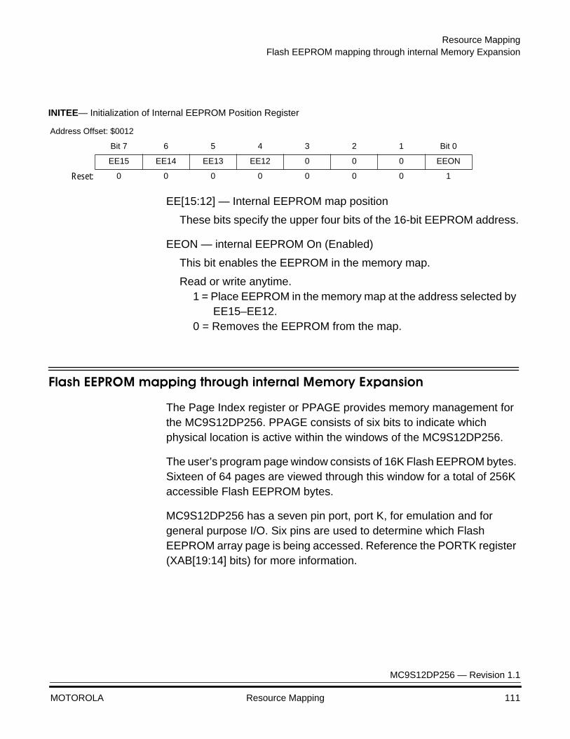
Resource MappingFlash EEPROM mapping through internal Memory Expansion
MC9S12DP256 — Revision 1.1
MOTOROLA Resource Mapping 111
EE[15:12] — Internal EEPROM map position
These bits specify the upper four bits of the 16-bit EEPROM address.
EEON — internal EEPROM On (Enabled)
This bit enables the EEPROM in the memory map.
Read or write anytime.1 = Place EEPROM in the memory map at the address selected by
EE15–EE12.0 = Removes the EEPROM from the map.
Flash EEPROM mapping through internal Memory Expansion
The Page Index register or PPAGE provides memory management for the MC9S12DP256. PPAGE consists of six bits to indicate which physical location is active within the windows of the MC9S12DP256.
The user’s program page window consists of 16K Flash EEPROM bytes. Sixteen of 64 pages are viewed through this window for a total of 256K accessible Flash EEPROM bytes.
MC9S12DP256 has a seven pin port, port K, for emulation and for general purpose I/O. Six pins are used to determine which Flash EEPROM array page is being accessed. Reference the PORTK register (XAB[19:14] bits) for more information.
INITEE— Initialization of Internal EEPROM Position Register
Address Offset: $0012
Bit 7 6 5 4 3 2 1 Bit 0
EE15 EE14 EE13 EE12 0 0 0 EEON
Reset: 0 0 0 0 0 0 0 1
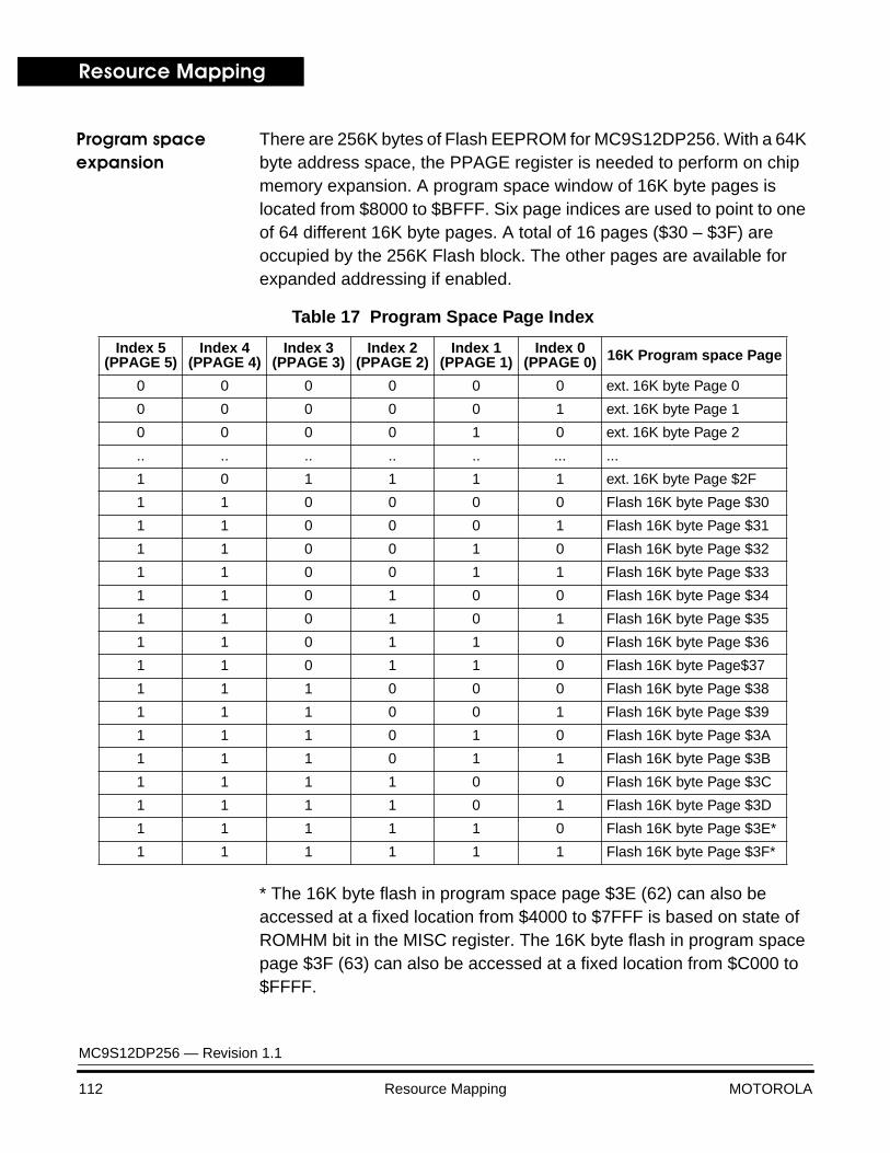
Resource Mapping
MC9S12DP256 — Revision 1.1
112 Resource Mapping MOTOROLA
Program space expansion
There are 256K bytes of Flash EEPROM for MC9S12DP256. With a 64K byte address space, the PPAGE register is needed to perform on chip memory expansion. A program space window of 16K byte pages is located from $8000 to $BFFF. Six page indices are used to point to one of 64 different 16K byte pages. A total of 16 pages ($30 – $3F) are occupied by the 256K Flash block. The other pages are available for expanded addressing if enabled.
* The 16K byte flash in program space page $3E (62) can also be accessed at a fixed location from $4000 to $7FFF is based on state of ROMHM bit in the MISC register. The 16K byte flash in program space page $3F (63) can also be accessed at a fixed location from $C000 to $FFFF.
Table 17 Program Space Page Index
Index 5(PPAGE 5)
Index 4(PPAGE 4)
Index 3(PPAGE 3)
Index 2(PPAGE 2)
Index 1(PPAGE 1)
Index 0(PPAGE 0) 16K Program space Page
0 0 0 0 0 0 ext. 16K byte Page 0
0 0 0 0 0 1 ext. 16K byte Page 1
0 0 0 0 1 0 ext. 16K byte Page 2
.. .. .. .. .. ... ...
1 0 1 1 1 1 ext. 16K byte Page $2F
1 1 0 0 0 0 Flash 16K byte Page $30
1 1 0 0 0 1 Flash 16K byte Page $31
1 1 0 0 1 0 Flash 16K byte Page $32
1 1 0 0 1 1 Flash 16K byte Page $33
1 1 0 1 0 0 Flash 16K byte Page $34
1 1 0 1 0 1 Flash 16K byte Page $35
1 1 0 1 1 0 Flash 16K byte Page $36
1 1 0 1 1 0 Flash 16K byte Page$37
1 1 1 0 0 0 Flash 16K byte Page $38
1 1 1 0 0 1 Flash 16K byte Page $39
1 1 1 0 1 0 Flash 16K byte Page $3A
1 1 1 0 1 1 Flash 16K byte Page $3B
1 1 1 1 0 0 Flash 16K byte Page $3C
1 1 1 1 0 1 Flash 16K byte Page $3D
1 1 1 1 1 0 Flash 16K byte Page $3E*
1 1 1 1 1 1 Flash 16K byte Page $3F*

Resource MappingFlash EEPROM mapping through internal Memory Expansion
MC9S12DP256 — Revision 1.1
MOTOROLA Resource Mapping 113
Page Index register descriptions
Read and write anytime
Writes do not change pin state when pin configured for page index emulation output.
This port is associated with the internal memory expansion emulation pins. When the port is not enabled to emulate the internal memory expansion, the port pins are used as general-purpose I/O. This register is not in the map in peripheral mode or in expanded modes while the EMK bit in the MODE register is set.
When inputs, these pins can be selected to be high impedance or pulled up based upon the state of the PUPKE bit in the PUCR register (in the MEBI).
Bit 7— Port K bit 7.
This bit is used as an emulation chip select signal for the emulation of the internal memory expansion, or as general purpose I/O, depending upon the state of the EMK bit in the MODE register. See Table 18 Expanded address decode for additional details on when this signal will be active.
The value on this pin during reset determines the reset state of the ROMON bit during reset into all expanded modes.
PORTK — Port K Data Register
Address Offset: $0032
Bit 7 6 5 4 3 2 1 Bit 0
Port: Bit 7 6 0 0 0 2 1 Bit 0
Reset: Unaffected by reset
Alt. pin function
ECS/ROMONE
0 XAB19 XAB18 XAB17 XAB16 XAB15 XAB14
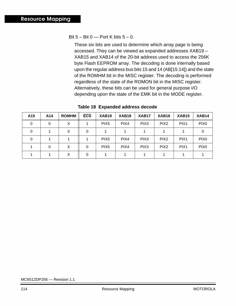
Resource Mapping
MC9S12DP256 — Revision 1.1
114 Resource Mapping MOTOROLA
Bit 5 – Bit 0 — Port K bits 5 – 0.
These six bits are used to determine which array page is being accessed. They can be viewed as expanded addresses XAB19 – XAB15 and XAB14 of the 20-bit address used to access the 256K byte Flash EEPROM array. The decoding is done internally based upon the regular address bus bits 15 and 14 (AB[15:14]) and the state of the ROMHM bit in the MISC register. The decoding is performed regardless of the state of the ROMON bit in the MISC register. Alternatively, these bits can be used for general purpose I/O depending upon the state of the EMK bit in the MODE register.
Table 18 Expanded address decode
A15 A14 ROMHM ECS XAB19 XAB18 XAB17 XAB16 XAB15 XAB14
0 0 X 1 PIX5 PIX4 PIX3 PIX2 PIX1 PIX0
0 1 0 0 1 1 1 1 1 0
0 1 1 1 PIX5 PIX4 PIX3 PIX2 PIX1 PIX0
1 0 X 0 PIX5 PIX4 PIX3 PIX2 PIX1 PIX0
1 1 X 0 1 1 1 1 1 1
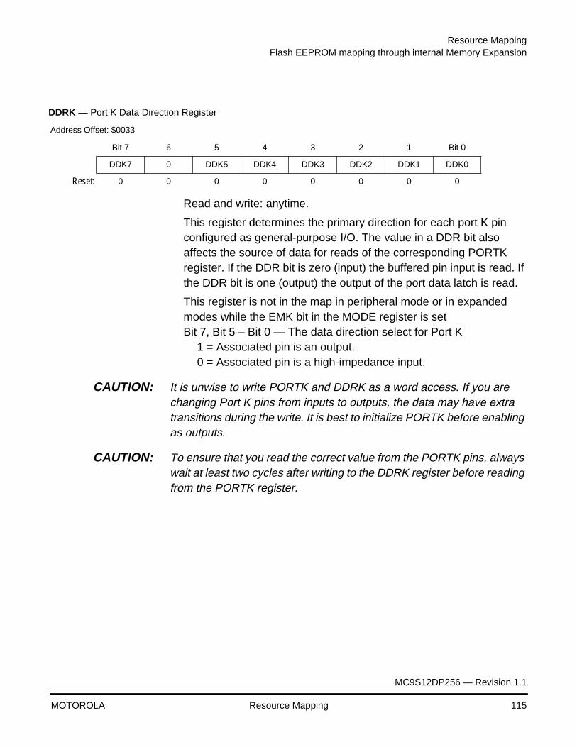
Resource MappingFlash EEPROM mapping through internal Memory Expansion
MC9S12DP256 — Revision 1.1
MOTOROLA Resource Mapping 115
Read and write: anytime.
This register determines the primary direction for each port K pin configured as general-purpose I/O. The value in a DDR bit also affects the source of data for reads of the corresponding PORTK register. If the DDR bit is zero (input) the buffered pin input is read. If the DDR bit is one (output) the output of the port data latch is read.
This register is not in the map in peripheral mode or in expanded modes while the EMK bit in the MODE register is setBit 7, Bit 5 – Bit 0 — The data direction select for Port K
1 = Associated pin is an output.0 = Associated pin is a high-impedance input.
CAUTION: It is unwise to write PORTK and DDRK as a word access. If you are changing Port K pins from inputs to outputs, the data may have extra transitions during the write. It is best to initialize PORTK before enabling as outputs.
CAUTION: To ensure that you read the correct value from the PORTK pins, always wait at least two cycles after writing to the DDRK register before reading from the PORTK register.
DDRK — Port K Data Direction Register
Address Offset: $0033
Bit 7 6 5 4 3 2 1 Bit 0
DDK7 0 DDK5 DDK4 DDK3 DDK2 DDK1 DDK0
Reset: 0 0 0 0 0 0 0 0
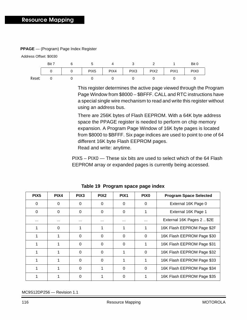
Resource Mapping
MC9S12DP256 — Revision 1.1
116 Resource Mapping MOTOROLA
This register determines the active page viewed through the Program Page Window from $8000 – $BFFF. CALL and RTC instructions have a special single wire mechanism to read and write this register without using an address bus.
There are 256K bytes of Flash EEPROM. With a 64K byte address space the PPAGE register is needed to perform on chip memory expansion. A Program Page Window of 16K byte pages is located from $8000 to $BFFF. Six page indices are used to point to one of 64 different 16K byte Flash EEPROM pages.Read and write: anytime.
PIX5 – PIX0 — These six bits are used to select which of the 64 Flash EEPROM array or expanded pages is currently being accessed.
PPAGE — (Program) Page Index Register
Address Offset: $0030
Bit 7 6 5 4 3 2 1 Bit 0
0 0 PIX5 PIX4 PIX3 PIX2 PIX1 PIX0
Reset: 0 0 0 0 0 0 0 0
Table 19 Program space page index
PIX5 PIX4 PIX3 PIX2 PIX1 PIX0 Program Space Selected
0 0 0 0 0 0 External 16K Page 0
0 0 0 0 0 1 External 16K Page 1
... ... ... ... ... ... External 16K Pages 2 .. $2E
1 0 1 1 1 1 16K Flash EEPROM Page $2F
1 1 0 0 0 0 16K Flash EEPROM Page $30
1 1 0 0 0 1 16K Flash EEPROM Page $31
1 1 0 0 1 0 16K Flash EEPROM Page $32
1 1 0 0 1 1 16K Flash EEPROM Page $33
1 1 0 1 0 0 16K Flash EEPROM Page $34
1 1 0 1 0 1 16K Flash EEPROM Page $35

Resource MappingFlash EEPROM mapping through internal Memory Expansion
MC9S12DP256 — Revision 1.1
MOTOROLA Resource Mapping 117
NOTE: In single chip mode pages are mirrored in the address map, i.e. page $30 occurs also as $00, $10 and $20. However it is advised that the user does not make use of this in order to stay compatible with future derivatives.
This register is used to designate the part ID. Each revision of the chip will have a unique value in the contents of this register.
Read anytime.
1 1 0 1 1 0 16K Flash EEPROM Page $36
1 1 0 1 1 1 16K Flash EEPROM Page $37
1 1 1 0 0 0 16K Flash EEPROM Page $38
1 1 1 0 0 1 16K Flash EEPROM Page $39
1 1 1 0 1 0 16K Flash EEPROM Page $3A
1 1 1 0 1 1 16K Flash EEPROM Page $3B
1 1 1 1 0 0 16K Flash EEPROM Page $3C
1 1 1 1 0 1 16K Flash EEPROM Page $3D
1 1 1 1 1 0 16K Flash EEPROM Page $3E
1 1 1 1 1 1 16K Flash EEPROM Page $3F
Table 19 Program space page index
PIX5 PIX4 PIX3 PIX2 PIX1 PIX0 Program Space Selected
PARTIDH — Part ID Register High
Address Offset: $001A
Bit 7 6 5 4 3 2 1 Bit 0
ID15 ID14 ID13 ID12 ID11 ID10 ID9 ID8
Reset: 0 0 0 0 0 0 0 0
PARTIDL — Part ID Register High
Address Offset: $001B
Bit 7 6 5 4 3 2 1 Bit 0
ID7 ID6 ID5 ID4 ID3 ID2 ID1 ID0
Reset: 0 0 0 0 0 0 0 0
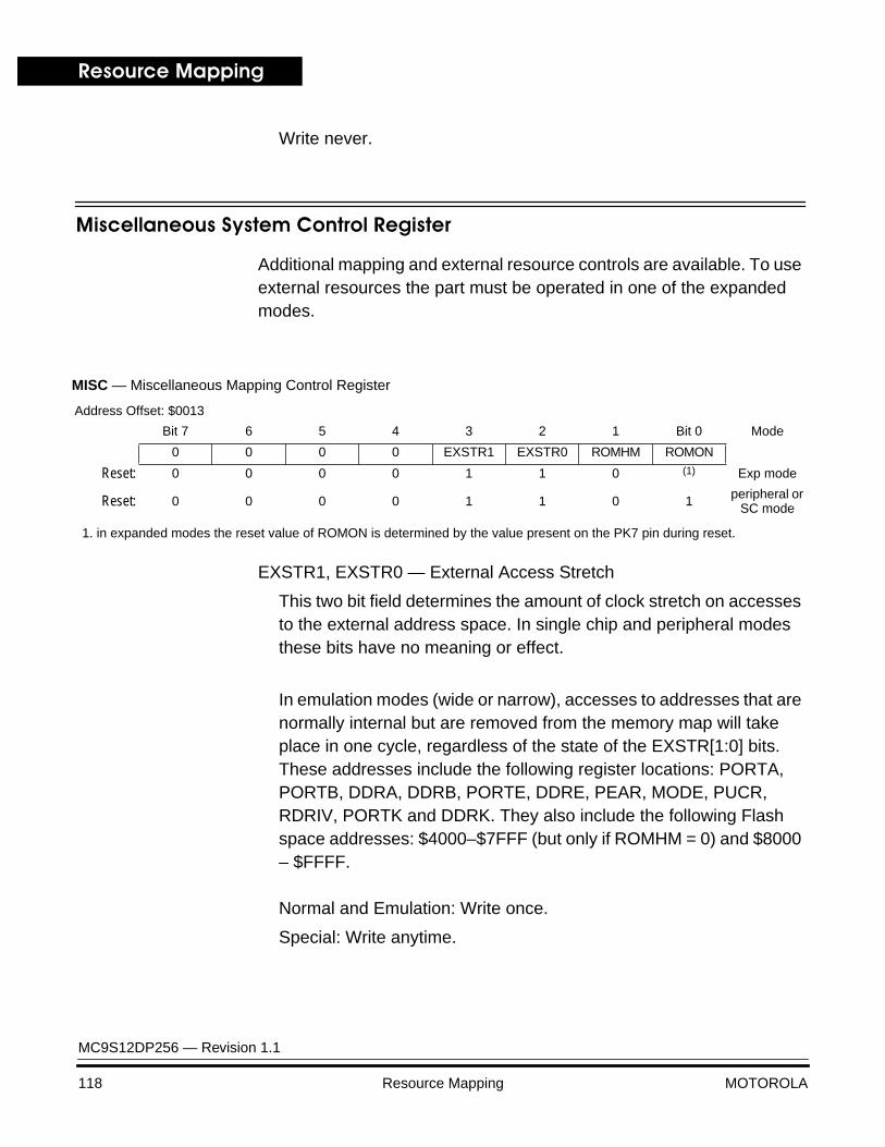
Resource Mapping
MC9S12DP256 — Revision 1.1
118 Resource Mapping MOTOROLA
Write never.
Miscellaneous System Control Register
Additional mapping and external resource controls are available. To use external resources the part must be operated in one of the expanded modes.
EXSTR1, EXSTR0 — External Access Stretch
This two bit field determines the amount of clock stretch on accesses to the external address space. In single chip and peripheral modes these bits have no meaning or effect.
In emulation modes (wide or narrow), accesses to addresses that are normally internal but are removed from the memory map will take place in one cycle, regardless of the state of the EXSTR[1:0] bits.These addresses include the following register locations: PORTA, PORTB, DDRA, DDRB, PORTE, DDRE, PEAR, MODE, PUCR, RDRIV, PORTK and DDRK. They also include the following Flash space addresses: $4000–$7FFF (but only if ROMHM = 0) and $8000 – $FFFF.
Normal and Emulation: Write once.
Special: Write anytime.
MISC — Miscellaneous Mapping Control Register
Address Offset: $0013
Bit 7 6 5 4 3 2 1 Bit 0 Mode
0 0 0 0 EXSTR1 EXSTR0 ROMHM ROMON
Reset: 0 0 0 0 1 1 0 (1) Exp mode
Reset: 0 0 0 0 1 1 0 1 peripheral or SC mode
1. in expanded modes the reset value of ROMON is determined by the value present on the PK7 pin during reset.
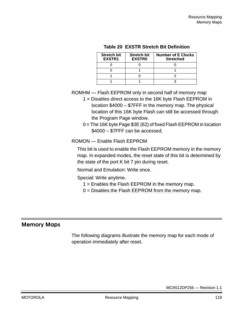
Resource MappingMemory Maps
MC9S12DP256 — Revision 1.1
MOTOROLA Resource Mapping 119
ROMHM — Flash EEPROM only in second half of memory map1 = Disables direct access to the 16K byte Flash EEPROM in
location $4000 – $7FFF in the memory map. The physical location of this 16K byte Flash can still be accessed through the Program Page window.
0 = The 16K byte Page $3E (62) of fixed Flash EEPROM in location $4000 – $7FFF can be accessed.
ROMON — Enable Flash EEPROM
This bit is used to enable the Flash EEPROM memory in the memory map. In expanded modes, the reset state of this bit is determined by the state of the port K bit 7 pin during reset.
Normal and Emulation: Write once.
Special: Write anytime.1 = Enables the Flash EEPROM in the memory map.0 = Disables the Flash EEPROM from the memory map.
Memory Maps
The following diagrams illustrate the memory map for each mode of operation immediately after reset.
Table 20 EXSTR Stretch Bit Definition
Stretch bit EXSTR1
Stretch bit EXSTR0
Number of E Clocks Stretched
0 0 0
0 1 1
1 0 2
1 1 3

Resource Mapping
MC9S12DP256 — Revision 1.1
120 Resource Mapping MOTOROLA
Figure 8 MC9S12DP256 Memory Map after reset
* Assuming that a ‘0’ was driven onto port K bit 7 during reset.
$0400
$0000
$1000
$4000
$8000
$C000
$FF00VECTORS
$FFFF
EXTERN
EXPANDED*
VECTORS
NORMALSINGLE CHIP
VECTORS
SPECIALSINGLE CHIP
REGISTERS(Mappable to any 2k Blockwithin the first 32K)
$0000
$03FF
$0000
$0FFF
4K Bytes EEPROM(Mappable to any 4K Block)
12K Bytes RAM(Mappable to any 16K
$1000
$3FFF
and alignable to top orbottom)
$4000
$7FFF
16K Fixed FlashPage $3E = 62(This is dependant on thestate of the ROMHM bit)
$8000
$BFFF
16K Page Window16 x 16K Flash EEPROMpages
$C000
$FFFF
16K Fixed FlashPage $3F = 63
$FF00
$FFFF
BDM(if active)
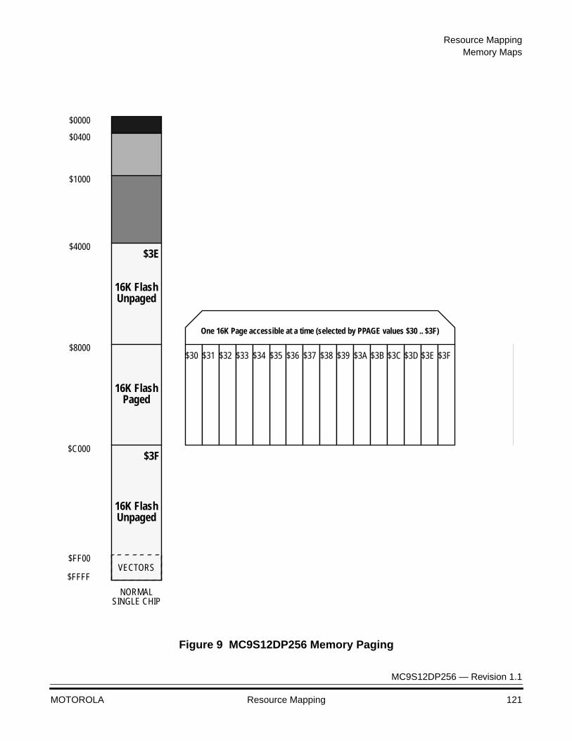
Resource MappingMemory Maps
MC9S12DP256 — Revision 1.1
MOTOROLA Resource Mapping 121
Figure 9 MC9S12DP256 Memory Paging
$0400
$0000
$1000
$4000
$8000
$C000
$FF00
$FFFFVECTORS
NORMALSINGLE CHIP
$3E
16K FlashUnpaged
16K FlashUnpaged
16K FlashPaged
$30 $31 $35 $36 $37$32 $33 $34 $38 $39 $3D $3E $3F$3A $3B $3C
$3F
One 16K Page accessible at a time (selected by PPAGE values $30 .. $3F)

Resource Mapping
MC9S12DP256 — Revision 1.1
122 Resource Mapping MOTOROLA

MC9S12DP256 — Revision 1.1
MOTOROLA Bus Control and Input/Output 123
Bus Control and Input/OutputBus Control and Input/Output
Contents
Introduction . . . . . . . . . . . . . . . . . . . . . . . . . . . . . . . . . . . . . . . . . . . . 123Detecting Access Type from External Signals . . . . . . . . . . . . . . . . . 123Stretched Bus Cycles . . . . . . . . . . . . . . . . . . . . . . . . . . . . . . . . . . . . 124PIPE Status Signals . . . . . . . . . . . . . . . . . . . . . . . . . . . . . . . . . . . . . 125Registers . . . . . . . . . . . . . . . . . . . . . . . . . . . . . . . . . . . . . . . . . . . . . . 127
Introduction
Internally the MC9S12DP256 has full 16-bit data paths, but depending upon the operating mode and control registers, the external multiplexed bus may be 8 or 16 bits. There are cases where 8-bit and 16-bit accesses can appear on adjacent cycles using the LSTRB signal to indicate 8- or 16-bit data.
Detecting Access Type from External Signals
The external signals LSTRB, R/W, and A0 indicate the type of bus access that is taking place. Accesses to the internal RAM module are the only type of access that produce LSTRB = A0 = 1, because the internal RAM is specifically designed to allow misaligned 16-bit accesses in a single cycle. In these cases the data for the address that was accessed is on the low half of the data bus and the data for address + 1 is on the high half of the data bus.
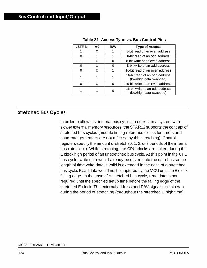
Bus Control and Input/Output
MC9S12DP256 — Revision 1.1
124 Bus Control and Input/Output MOTOROLA
Stretched Bus Cycles
In order to allow fast internal bus cycles to coexist in a system with slower external memory resources, the STAR12 supports the concept of stretched bus cycles (module timing reference clocks for timers and baud rate generators are not affected by this stretching). Control registers specify the amount of stretch (0, 1, 2, or 3 periods of the internal bus-rate clock). While stretching, the CPU clocks are halted during the E clock high period of an unstretched bus cycle. At this point in the CPU bus cycle, write data would already be driven onto the data bus so the length of time write data is valid is extended in the case of a stretched bus cycle. Read data would not be captured by the MCU until the E clock falling edge. In the case of a stretched bus cycle, read data is not required until the specified setup time before the falling edge of the stretched E clock. The external address and R/W signals remain valid during the period of stretching (throughout the stretched E high time).
Table 21 Access Type vs. Bus Control Pins
LSTRB A0 R/W Type of Access1 0 1 8-bit read of an even address0 1 1 8-bit read of an odd address1 0 0 8-bit write of an even address0 1 0 8-bit write of an odd address0 0 1 16-bit read of an even address
1 1 116-bit read of an odd address
(low/high data swapped)0 0 0 16-bit write to an even address
1 1 016-bit write to an odd address
(low/high data swapped)
Bus Control and Input/OutputPIPE Status Signals
MC9S12DP256 — Revision 1.1
MOTOROLA Bus Control and Input/Output 125
PIPE Status Signals
PIPE status signals IPIPE[1:0] provide information about data movement in the queue and indicate when the CPU begins to execute instructions. This makes it possible to monitor CPU activity on a cycle-by-cycle basis for debugging. Information available on the IPIPE[1:0] pins is time multiplexed.
Data movement (valid during E-clock high) is represented by two states:
• Advance and load from bus – This state means the queue shifts up one stage with stage 1 being filled with the instruction on the bus.
• No movement – This state means there is no data shifting in the queue.
The execution start (valid during E-clock low) is represented by four states:
• No start – This state indicates a continuation of the current instruction.
• Start interrupt – This state indicates that an interrupt sequence has begun.
NOTE: The start interrupt state is indicated when an external signal alters program flow (i.e. interrupt request, force or tag). SWI and TRAP instructions in the instruction pipe are indicated as start even or start odd depending on their alignment. In this case, the SWI and TRAP instructions are part of the normal program flow. Since they are present in the queue, they may be tracked in an external pipe rebuild. An external event that interrupts program flow is indeterministic. Program data is not present in the queue until after the vector jump.
• Start even – This state indicates the current opcode is located in the top of the queue, high byte.
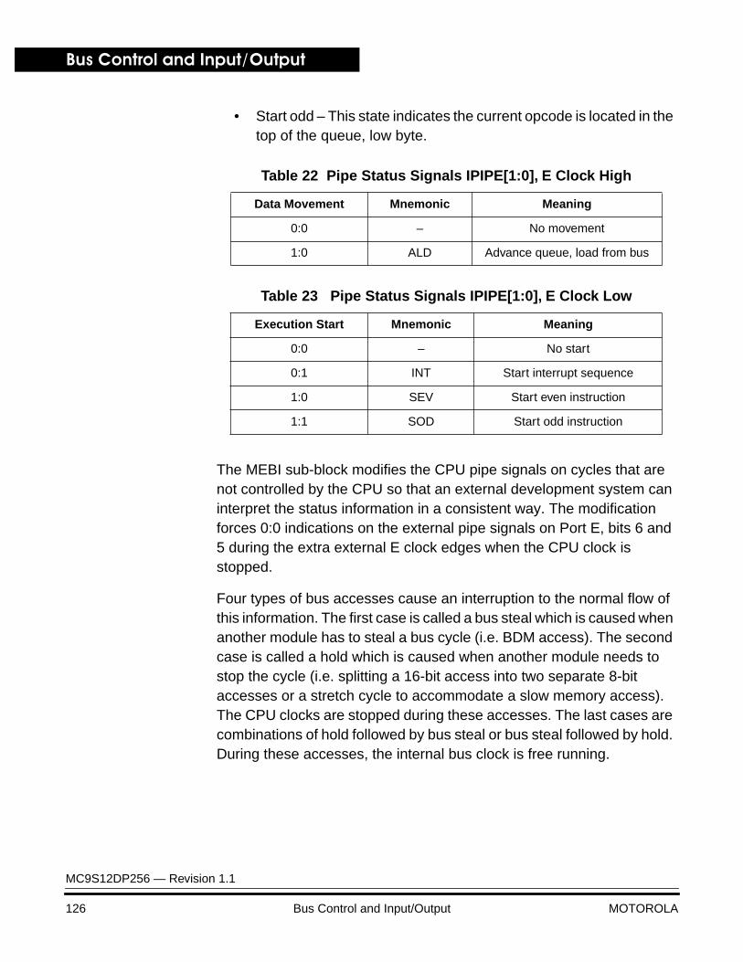
Bus Control and Input/Output
MC9S12DP256 — Revision 1.1
126 Bus Control and Input/Output MOTOROLA
• Start odd – This state indicates the current opcode is located in the top of the queue, low byte.
The MEBI sub-block modifies the CPU pipe signals on cycles that are not controlled by the CPU so that an external development system can interpret the status information in a consistent way. The modification forces 0:0 indications on the external pipe signals on Port E, bits 6 and 5 during the extra external E clock edges when the CPU clock is stopped.
Four types of bus accesses cause an interruption to the normal flow of this information. The first case is called a bus steal which is caused when another module has to steal a bus cycle (i.e. BDM access). The second case is called a hold which is caused when another module needs to stop the cycle (i.e. splitting a 16-bit access into two separate 8-bit accesses or a stretch cycle to accommodate a slow memory access). The CPU clocks are stopped during these accesses. The last cases are combinations of hold followed by bus steal or bus steal followed by hold. During these accesses, the internal bus clock is free running.
Table 22 Pipe Status Signals IPIPE[1:0], E Clock High
Data Movement Mnemonic Meaning
0:0 – No movement
1:0 ALD Advance queue, load from bus
Table 23 Pipe Status Signals IPIPE[1:0], E Clock Low
Execution Start Mnemonic Meaning
0:0 – No start
0:1 INT Start interrupt sequence
1:0 SEV Start even instruction
1:1 SOD Start odd instruction
Bus Control and Input/OutputRegisters
MC9S12DP256 — Revision 1.1
MOTOROLA Bus Control and Input/Output 127
Registers
Not all registers are visible in the MC9S12DP256 memory map under certain conditions.
In special peripheral mode the first 16 registers associated with bus expansion are removed from the memory map.
In expanded modes, some or all of port A, port B, and port E are used for expansion buses and control signals. In order to allow emulation of the single-chip functions of these ports, some of these registers must be rebuilt in an external port replacement unit. In any expanded mode, port A, and port B, are used for address and data lines so registers for these ports, as well as the data direction registers for these ports, are removed from the on-chip memory map and become external accesses.
In any expanded mode, port E pins may be needed for bus control (e.g., ECLK, R/W). To regain the single-chip functions of port E, the emulate port E (EME) control bit in the MODE register may be set. In this special case of expanded mode and EME set, PORTE and DDRE registers are removed from the on-chip memory map and become external accesses so port E may be rebuilt externally.
Bus Control and Input/Output
MC9S12DP256 — Revision 1.1
128 Bus Control and Input/Output MOTOROLA
Port A bits 7 through 0 are associated with address lines A15 through A8 respectively and data lines D15/D7 through D8/D0 respectively. When this port is not used for external addresses such as in single-chip mode, these pins can be used as general purpose I/O. Data Direction Register A (DDRA) determines the primary direction of each pin. DDRA also determines the source of data for a read of PORTA.
This register is not in the on-chip map in expanded and peripheral modes.
CAUTION: To ensure that you read the value present on the PORTA pins, always wait at least two cycles after writing to the DDRA register before reading from the PORTA register.
Read and write: anytime (provided this register is in the map).
PORTA — Port A Register
Address Offset: $0000
Bit 7 6 5 4 3 2 1 Bit 0
Single Chip BIT 7 6 5 4 3 2 1 BIT 0
Reset: Unaffected by reset
Expanded & Periph:
ADDR15/ DATA15
ADDR14/ DATA14
ADDR13/ DATA13
ADDR12/ DATA12
ADDR11/ DATA11
ADDR10/ DATA10
ADDR9/ DATA9
ADDR8/ DATA8
Expandednarrow
ADDR15/ DATA15/DATA7
ADDR14/ DATA14/DATA6
ADDR13/ DATA13/DATA5
ADDR12/ DATA12/DATA4
ADDR11/ DATA11/DATA3
ADDR10/ DATA10/DATA2
ADDR9/ DATA9/DATA1
ADDR8/ DATA8/DATA0

Bus Control and Input/OutputRegisters
MC9S12DP256 — Revision 1.1
MOTOROLA Bus Control and Input/Output 129
This register controls the data direction for Port A. When Port A is operating as a general purpose I/O port, DDRA determines the primary direction for each Port A pin. A “1” causes the associated port pin to be an output and a “0” causes the associated pin to be a high-impedance input. The value in a DDR bit also affects the source of data for reads of the corresponding PORTA register. If the DDR bit is zero (input) the buffered pin input is read. If the DDR bit is one (output) the output of the port data latch is read.
This register is not in the on-chip map in expanded and peripheral modes. It is reset to $00 so the DDR does not override the three-state control signals.
Read and write: anytime (provided this register is in the map).
DDRA7–0 — Data Direction Port A0 = Configure the corresponding I/O pin as an input1 = Configure the corresponding I/O as an output
Port B bits 7 through 0 are associated with address lines A7 through A0 respectively and data lines D7 through D0 respectively. When this port is not used for external addresses, such as in single-chip mode,
DDRA — Port A Data Direction Register
Address Offset: $0002
Bit 7 6 5 4 3 2 1 Bit 0
BIT 7 6 5 4 3 2 1 BIT 0
Reset: 0 0 0 0 0 0 0 0
PORTB — Port B Register
Address Offset: $0001
Bit 7 6 5 4 3 2 1 Bit 0
Single Chip Bit 7 6 5 4 3 2 1 Bit 0
Reset: Unaffected by reset
Expanded& Periph:
ADDR7/DATA7
ADDR6/DATA6
ADDR5/DATA5
ADDR4/DATA4
ADDR3/DATA3
ADDR2/DATA2
ADDR1/DATA1
ADDR0/DATA0
Expandednarrow
ADDR7 ADDR6 ADDR5 ADDR4 ADDR3 ADDR2 ADDR1 ADDR0
Bus Control and Input/Output
MC9S12DP256 — Revision 1.1
130 Bus Control and Input/Output MOTOROLA
these pins can be used as general purpose I/O. Data Direction Register B (DDRB) determines the primary direction of each pin. DDRB also determines the source of data for a read of PORTB.
This register is not in the on-chip map in expanded and peripheral modes.
CAUTION: To ensure that you read the value present on the PORTB pins, always wait at least two cycles after writing to the DDRB register before reading from the PORTB register.
Read and write: anytime (provided this register is in the map).

Bus Control and Input/OutputRegisters
MC9S12DP256 — Revision 1.1
MOTOROLA Bus Control and Input/Output 131
This register controls the data direction for Port B. When Port B is operating as a general purpose I/O port, DDRB determines the primary direction for each Port B pin. A “1” causes the associated port pin to be an output and a “0” causes the associated pin to be a high-impedance input. The value in a DDR bit also affects the source of data for reads of the corresponding PORTB register. If the DDR bit is zero (input) the buffered pin input is read. If the DDR bit is one (output) the output of the port data latch is read.
This register is not in the on-chip map in expanded and peripheral modes. It is reset to $00 so the DDR does not override the three-state control signals.
Read and write: anytime (provided this register is in the map).
DDRB7–0 — Data Direction Port B0 = Configure the corresponding I/O pin as an input1 = Configure the corresponding I/O pin as an output
DDRB — Port B Data Direction Register
Address Offset: $0003
Bit 7 6 5 4 3 2 1 Bit 0
Bit 7 6 5 4 3 2 1 Bit 0
Reset: 0 0 0 0 0 0 0 0
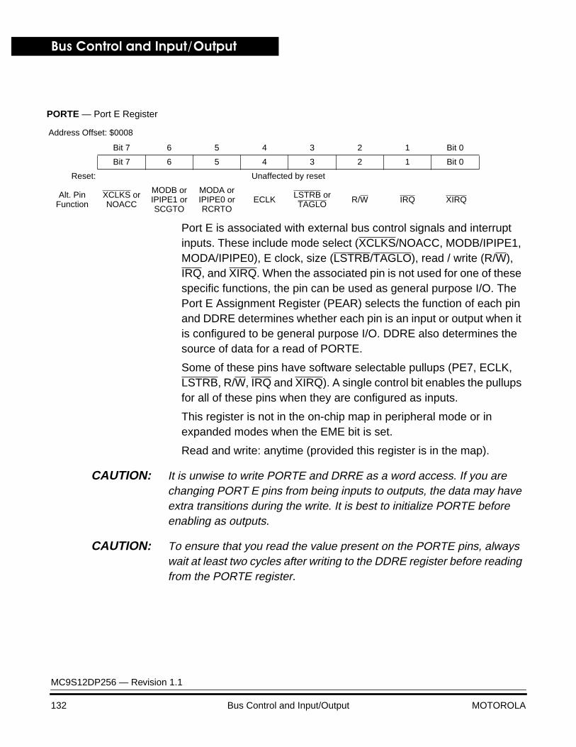
Bus Control and Input/Output
MC9S12DP256 — Revision 1.1
132 Bus Control and Input/Output MOTOROLA
Port E is associated with external bus control signals and interrupt inputs. These include mode select (XCLKS/NOACC, MODB/IPIPE1, MODA/IPIPE0), E clock, size (LSTRB/TAGLO), read / write (R/W), IRQ, and XIRQ. When the associated pin is not used for one of these specific functions, the pin can be used as general purpose I/O. The Port E Assignment Register (PEAR) selects the function of each pin and DDRE determines whether each pin is an input or output when it is configured to be general purpose I/O. DDRE also determines the source of data for a read of PORTE.
Some of these pins have software selectable pullups (PE7, ECLK, LSTRB, R/W, IRQ and XIRQ). A single control bit enables the pullups for all of these pins when they are configured as inputs.
This register is not in the on-chip map in peripheral mode or in expanded modes when the EME bit is set.
Read and write: anytime (provided this register is in the map).
CAUTION: It is unwise to write PORTE and DRRE as a word access. If you are changing PORT E pins from being inputs to outputs, the data may have extra transitions during the write. It is best to initialize PORTE before enabling as outputs.
CAUTION: To ensure that you read the value present on the PORTE pins, always wait at least two cycles after writing to the DDRE register before reading from the PORTE register.
PORTE — Port E Register
Address Offset: $0008
Bit 7 6 5 4 3 2 1 Bit 0
Bit 7 6 5 4 3 2 1 Bit 0
Reset: Unaffected by reset
Alt. Pin Function
XCLKS or NOACC
MODB or IPIPE1 or SCGTO
MODA or IPIPE0 or RCRTO
ECLK LSTRB orTAGLO R/W IRQ XIRQ

Bus Control and Input/OutputRegisters
MC9S12DP256 — Revision 1.1
MOTOROLA Bus Control and Input/Output 133
Data Direction Register E is associated with Port E. For bits in Port E that are configured as general purpose I/O lines, DDRE determines the primary direction of each of these pins. A “1” causes the associated bit to be an output and a “0” causes the associated bit to be an input. Port E bit 1 (associated with IRQ) and bit 0 (associated with XIRQ) cannot be configured as outputs. Port E, bit 1, and bit 0 can be read regardless of whether the alternate interrupt function is enabled. The value in a DDR bit also affects the source of data for reads of the corresponding PORTE register. If the DDR bit is zero (input) the buffered pin input is read. If the DDR bit is one (output) the output of the port data latch is read.
This register is not in the on-chip map in peripheral mode. It is also not in the map in expanded modes while the EME control bit is set.
Read and write: anytime (provided this register is in the map).
DDRE7–2 — Data Direction Port E0 = Configure the corresponding I/O pin as an input1 = Configure the corresponding I/O pin as an output
DDRE — Port E Data Direction Register
Address Offset: $0009
Bit 7 6 5 4 3 2 1 Bit 0
Bit 7 6 5 4 3 Bit 2 0 0
Reset: 0 0 0 0 0 0 0 0
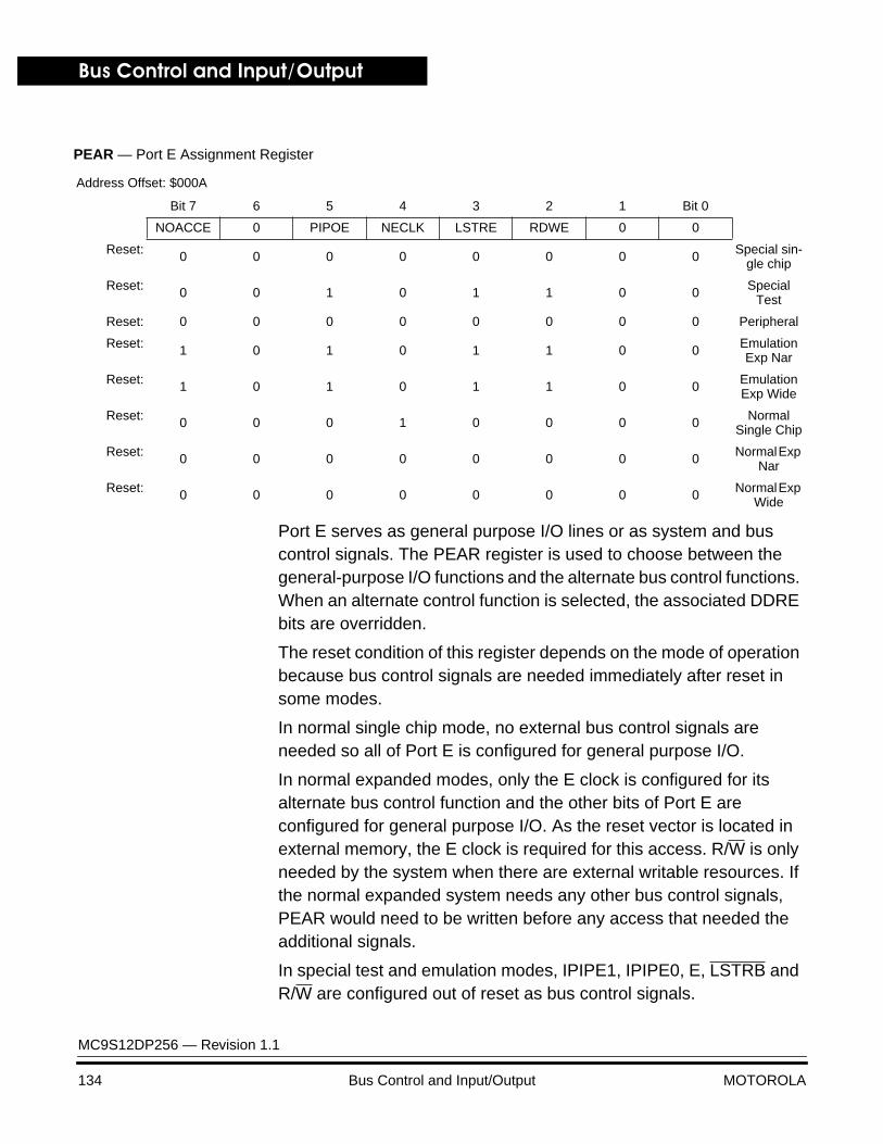
Bus Control and Input/Output
MC9S12DP256 — Revision 1.1
134 Bus Control and Input/Output MOTOROLA
Port E serves as general purpose I/O lines or as system and bus control signals. The PEAR register is used to choose between the general-purpose I/O functions and the alternate bus control functions. When an alternate control function is selected, the associated DDRE bits are overridden.
The reset condition of this register depends on the mode of operation because bus control signals are needed immediately after reset in some modes.
In normal single chip mode, no external bus control signals are needed so all of Port E is configured for general purpose I/O.
In normal expanded modes, only the E clock is configured for its alternate bus control function and the other bits of Port E are configured for general purpose I/O. As the reset vector is located in external memory, the E clock is required for this access. R/W is only needed by the system when there are external writable resources. If the normal expanded system needs any other bus control signals, PEAR would need to be written before any access that needed the additional signals.
In special test and emulation modes, IPIPE1, IPIPE0, E, LSTRB and R/W are configured out of reset as bus control signals.
PEAR — Port E Assignment Register
Address Offset: $000A
Bit 7 6 5 4 3 2 1 Bit 0
NOACCE 0 PIPOE NECLK LSTRE RDWE 0 0
Reset: 0 0 0 0 0 0 0 0 Special sin-gle chip
Reset: 0 0 1 0 1 1 0 0 Special Test
Reset: 0 0 0 0 0 0 0 0 Peripheral
Reset: 1 0 1 0 1 1 0 0 Emulation Exp Nar
Reset: 1 0 1 0 1 1 0 0 Emulation Exp Wide
Reset: 0 0 0 1 0 0 0 0 Normal Single Chip
Reset: 0 0 0 0 0 0 0 0 Normal Exp Nar
Reset: 0 0 0 0 0 0 0 0 Normal Exp Wide

Bus Control and Input/OutputRegisters
MC9S12DP256 — Revision 1.1
MOTOROLA Bus Control and Input/Output 135
NOACCE — CPU No Access Output Enable
Normal: write once
Emulation: write never
Special: write anytime1 = The associated pin (Port E bit 7) is output and indicates
whether the cycle is a CPU free cycle.0 = The associated pin (Port E bit 7) is general purpose I/O.
This bit has no effect in single chip or peripheral modes.
PIPOE — Pipe Status Signal Output Enable
Normal: write once
Emulation: write never
Special: write anytime.1 = The associated pins (Port E bits 6:5) are outputs and indicate
the state of the instruction queue0 = The associated pins (Port E bits 6:5) are general purpose I/O.
This bit has no effect in single chip or peripheral modes.
NECLK — No External E Clock
Normal and Special: write anytime
Emulation: write never1 = The associated pin (Port E bit 4) is a general purpose I/O pin. 0 = The associated pin (Port E bit 4) is the external E clock pin.
External E clock is free-running if ESTR=0.
External E clock is available as an output in all modes.

Bus Control and Input/Output
MC9S12DP256 — Revision 1.1
136 Bus Control and Input/Output MOTOROLA
LSTRE — Low Strobe (LSTRB) Enable
Normal: write once
Emulation: write never
Special: write anytime. 1 = The associated pin (Port E bit 3) is configured as the LSTRB
bus control output. If BDM tagging is enabled, TAGLO is multiplexed in on the data cycle and LSTRB is driven out on the address cycle.
0 = The associated pin (Port E bit 3) is a general purpose I/O pin.
This bit has no effect in single chip, peripheral or normal expanded narrow modes.
NOTE: LSTRB is used during external writes. After reset in normal expanded mode, LSTRB is disabled to provide an extra I/O pin. If LSTRB is needed, it should be enabled before any external writes. External reads do not normally need LSTRB because all 16 data bits can be driven even if the MCU only needs 8 bits of data
RDWE — Read / Write Enable
Normal: write once
Emulation: write never
Special: write anytime1 = The associated pin (Port E bit 2) is configured as the R/W pin.0 = The associated pin (Port E bit 2) is a general purpose I/O pin.
This bit has no effect in single chip or peripheral modes.
NOTE: R/W is used for external writes. After reset in normal expanded mode, R/W is disabled to provide an extra I/O pin. If R/W is needed it should be enabled before any external writes.
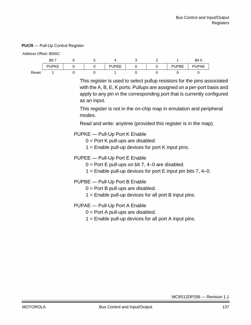
Bus Control and Input/OutputRegisters
MC9S12DP256 — Revision 1.1
MOTOROLA Bus Control and Input/Output 137
This register is used to select pullup resistors for the pins associated with the A, B, E, K ports. Pullups are assigned on a per-port basis and apply to any pin in the corresponding port that is currently configured as an input.
This register is not in the on-chip map in emulation and peripheral modes.
Read and write: anytime (provided this register is in the map).
PUPKE — Pull-Up Port K Enable0 = Port K pull-ups are disabled.1 = Enable pull-up devices for port K input pins.
PUPEE — Pull-Up Port E Enable0 = Port E pull-ups on bit 7, 4–0 are disabled.1 = Enable pull-up devices for port E input pin bits 7, 4–0.
PUPBE — Pull-Up Port B Enable0 = Port B pull-ups are disabled.1 = Enable pull-up devices for all port B input pins.
PUPAE — Pull-Up Port A Enable0 = Port A pull-ups are disabled.1 = Enable pull-up devices for all port A input pins.
PUCR — Pull-Up Control Register
Address Offset: $000C
Bit 7 6 5 4 3 2 1 Bit 0
PUPKE 0 0 PUPEE 0 0 PUPBE PUPAE
Reset: 1 0 0 1 0 0 0 0
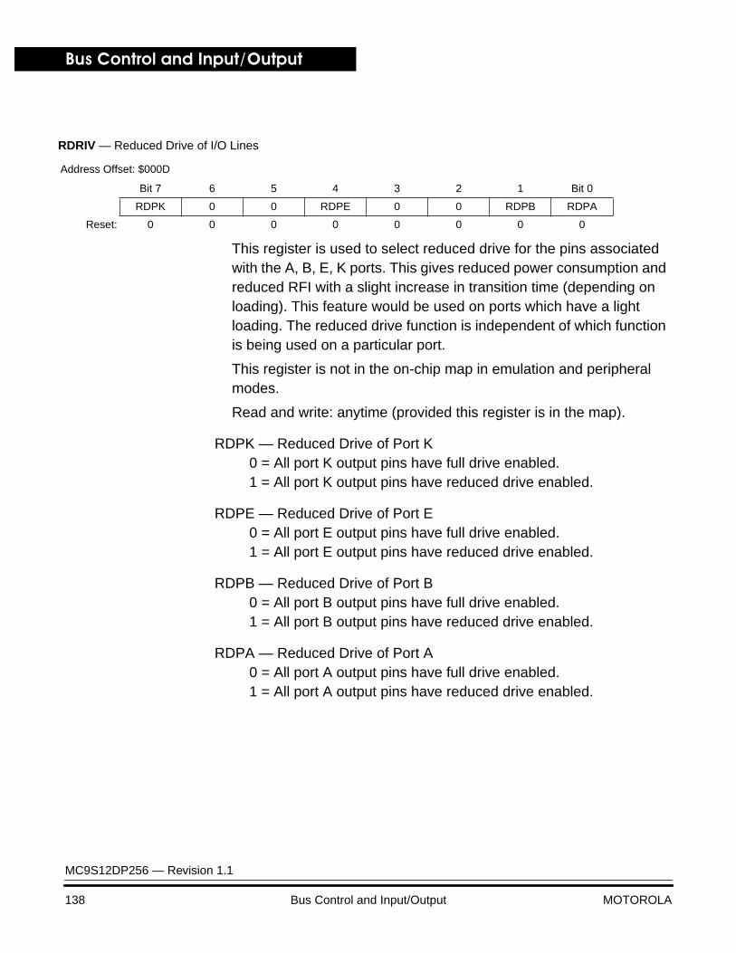
Bus Control and Input/Output
MC9S12DP256 — Revision 1.1
138 Bus Control and Input/Output MOTOROLA
This register is used to select reduced drive for the pins associated with the A, B, E, K ports. This gives reduced power consumption and reduced RFI with a slight increase in transition time (depending on loading). This feature would be used on ports which have a light loading. The reduced drive function is independent of which function is being used on a particular port.
This register is not in the on-chip map in emulation and peripheral modes.
Read and write: anytime (provided this register is in the map).
RDPK — Reduced Drive of Port K0 = All port K output pins have full drive enabled.1 = All port K output pins have reduced drive enabled.
RDPE — Reduced Drive of Port E0 = All port E output pins have full drive enabled.1 = All port E output pins have reduced drive enabled.
RDPB — Reduced Drive of Port B0 = All port B output pins have full drive enabled.1 = All port B output pins have reduced drive enabled.
RDPA — Reduced Drive of Port A0 = All port A output pins have full drive enabled.1 = All port A output pins have reduced drive enabled.
RDRIV — Reduced Drive of I/O Lines
Address Offset: $000D
Bit 7 6 5 4 3 2 1 Bit 0
RDPK 0 0 RDPE 0 0 RDPB RDPA
Reset: 0 0 0 0 0 0 0 0
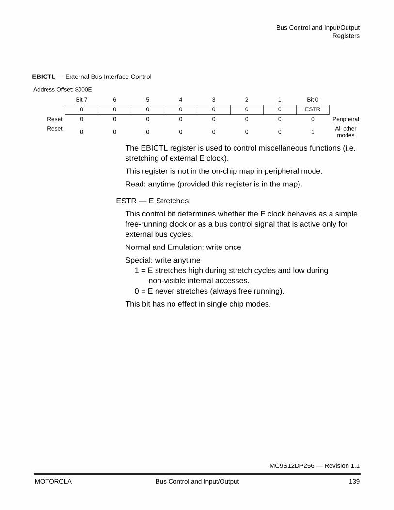
Bus Control and Input/OutputRegisters
MC9S12DP256 — Revision 1.1
MOTOROLA Bus Control and Input/Output 139
The EBICTL register is used to control miscellaneous functions (i.e. stretching of external E clock).
This register is not in the on-chip map in peripheral mode.
Read: anytime (provided this register is in the map).
ESTR — E Stretches
This control bit determines whether the E clock behaves as a simple free-running clock or as a bus control signal that is active only for external bus cycles.
Normal and Emulation: write once
Special: write anytime1 = E stretches high during stretch cycles and low during
non-visible internal accesses.0 = E never stretches (always free running).
This bit has no effect in single chip modes.
EBICTL — External Bus Interface Control
Address Offset: $000E
Bit 7 6 5 4 3 2 1 Bit 0
0 0 0 0 0 0 0 ESTR
Reset: 0 0 0 0 0 0 0 0 Peripheral
Reset: 0 0 0 0 0 0 0 1 All other modes

Bus Control and Input/Output
MC9S12DP256 — Revision 1.1
140 Bus Control and Input/Output MOTOROLA

MC9S12DP256 — Revision 1.1
MOTOROLA Resets and Interrupts 141
Resets and InterruptsResets and Interrupts
Contents
Introduction . . . . . . . . . . . . . . . . . . . . . . . . . . . . . . . . . . . . . . . . . . . . 141Register Map. . . . . . . . . . . . . . . . . . . . . . . . . . . . . . . . . . . . . . . . . . . 142Exception Priority . . . . . . . . . . . . . . . . . . . . . . . . . . . . . . . . . . . . . . . 142Maskable interrupts. . . . . . . . . . . . . . . . . . . . . . . . . . . . . . . . . . . . . . 143Latching of Interrupts . . . . . . . . . . . . . . . . . . . . . . . . . . . . . . . . . . . . 144Register Descriptions . . . . . . . . . . . . . . . . . . . . . . . . . . . . . . . . . . . . 147Resets . . . . . . . . . . . . . . . . . . . . . . . . . . . . . . . . . . . . . . . . . . . . . . . . 151Effects of Reset. . . . . . . . . . . . . . . . . . . . . . . . . . . . . . . . . . . . . . . . . 155Register Stacking . . . . . . . . . . . . . . . . . . . . . . . . . . . . . . . . . . . . . . . 157
Introduction
STAR12 exceptions include resets and interrupts. Each exception has an associated 16-bit vector, which points to the memory location where the routine that handles the exception is located. Vectors are stored in the upper 128 bytes of the standard 64K byte address map.
The six highest vector addresses are used for resets and non-maskable interrupt sources. The remainder of the vectors are used for maskable interrupts, and all must be initialized to point to the address of the appropriate service routine.
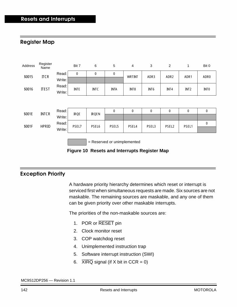
Resets and Interrupts
MC9S12DP256 — Revision 1.1
142 Resets and Interrupts MOTOROLA
Register Map
Figure 10 Resets and Interrupts Register Map
Exception Priority
A hardware priority hierarchy determines which reset or interrupt is serviced first when simultaneous requests are made. Six sources are not maskable. The remaining sources are maskable, and any one of them can be given priority over other maskable interrupts.
The priorities of the non-maskable sources are:
1. POR or RESET pin
2. Clock monitor reset
3. COP watchdog reset
4. Unimplemented instruction trap
5. Software interrupt instruction (SWI)
6. XIRQ signal (if X bit in CCR = 0)
Address Register Name Bit 7 6 5 4 3 2 1 Bit 0
$0015 ITCRRead: 0 0 0
WRTINT ADR3 ADR2 ADR1 ADR0Write:
$0016 ITESTRead:
INTE INTC INTA INT8 INT6 INT4 INT2 INT0Write:
$001E INTCRRead:
IRQE IRQEN0 0 0 0 0 0
Write:
$001F HPRIORead:
PSEL7 PSEL6 PSEL5 PSEL4 PSEL3 PSEL2 PSEL10
Write:
= Reserved or unimplemented
Resets and InterruptsMaskable interrupts
MC9S12DP256 — Revision 1.1
MOTOROLA Resets and Interrupts 143
Maskable interrupts
Maskable interrupt sources include on-chip peripheral systems and external interrupt service requests. Interrupts from these sources are recognized when the global interrupt mask bit (I) in the CCR is cleared. The default state of the I bit out of reset is one, but it can be written at any time.
Interrupt sources are prioritized by default but any one maskable interrupt source may be assigned the highest priority by means of the HPRIO register. The relative priorities of the other sources remain the same.
An interrupt that is assigned highest priority is still subject to global masking by the I bit in the CCR, or by any associated local bits. Interrupt vectors are not affected by priority assignment. HPRIO can only be written while the I bit is set (interrupts inhibited). Table 24 lists interrupt sources and vectors in default order of priority. Before masking an interrupt by clearing the corresponding local enable bit, it is required to set the I-bit to avoid an SWI.

Resets and Interrupts
MC9S12DP256 — Revision 1.1
144 Resets and Interrupts MOTOROLA
Latching of Interrupts
XIRQ is always level triggered and IRQ can be selected as a level triggered interrupt. These level triggered interrupt pins should only be released during the appropriate interrupt service routine. Generally the interrupt service routine will handshake with the interrupting logic to release the pin. In this way, the MCU will never start the interrupt service sequence only to determine that there is no longer an interrupt source. In event that this does occur the trap vector will be taken.
If IRQ is selected as an edge triggered interrupt, the hold time of the level after the active edge is independent of when the interrupt is serviced. As long as the minimum hold time is met, the interrupt will be latched inside the MCU. In this case the IRQ edge interrupt latch is cleared automatically when the interrupt is serviced.
All of the remaining interrupts are latched by the MCU with a flag bit. These interrupt flags should be cleared during an interrupt service routine or when interrupts are masked by the I bit. By doing this, the MCU will never get an unknown interrupt source and take the trap vector.
Table 24 Interrupt Vector Table
Vector Address Interrupt Source CCR Mask Local Enable HPRIO Value
to Elevate
$FFFE, $FFFF Reset None None –
$FFFC, $FFFD Clock Monitor fail reset None COPCTL (CME, FCME) –
$FFFA, $FFFB COP failure reset None COP rate select –
$FFF8, $FFF9 Unimplemented instruction trap None None –
$FFF6, $FFF7 SWI None None –
$FFF4, $FFF5 XIRQ X-Bit None –
$FFF2, $FFF3 IRQ I-Bit INTCR (IRQEN) $F2
$FFF0, $FFF1 Real Time Interrupt I-Bit CRGINT (RTIE) $F0
$FFEE, $FFEF Timer channel 0 I-Bit TMSK1 (C0I) $EE
$FFEC, $FFED Timer channel 1 I-Bit TMSK1 (C1I) $EC
$FFEA, $FFEB Timer channel 2 I-Bit TMSK1 (C2I) $EA
$FFE8, $FFE9 Timer channel 3 I-Bit TMSK1 (C3I) $E8
$FFE6, $FFE7 Timer channel 4 I-Bit TMSK1 (C4I) $E6
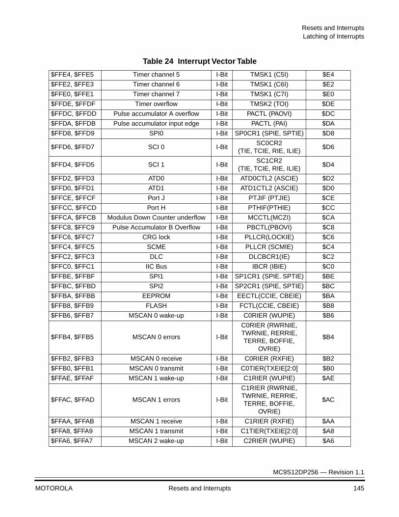
Resets and InterruptsLatching of Interrupts
MC9S12DP256 — Revision 1.1
MOTOROLA Resets and Interrupts 145
$FFE4, $FFE5 Timer channel 5 I-Bit TMSK1 (C5I) $E4
$FFE2, $FFE3 Timer channel 6 I-Bit TMSK1 (C6I) $E2
$FFE0, $FFE1 Timer channel 7 I-Bit TMSK1 (C7I) $E0
$FFDE, $FFDF Timer overflow I-Bit TMSK2 (TOI) $DE
$FFDC, $FFDD Pulse accumulator A overflow I-Bit PACTL (PAOVI) $DC
$FFDA, $FFDB Pulse accumulator input edge I-Bit PACTL (PAI) $DA
$FFD8, $FFD9 SPI0 I-Bit SP0CR1 (SPIE, SPTIE) $D8
$FFD6, $FFD7 SCI 0 I-BitSC0CR2
(TIE, TCIE, RIE, ILIE)$D6
$FFD4, $FFD5 SCI 1 I-BitSC1CR2
(TIE, TCIE, RIE, ILIE)$D4
$FFD2, $FFD3 ATD0 I-Bit ATD0CTL2 (ASCIE) $D2
$FFD0, $FFD1 ATD1 I-Bit ATD1CTL2 (ASCIE) $D0
$FFCE, $FFCF Port J I-Bit PTJIF (PTJIE) $CE
$FFCC, $FFCD Port H I-Bit PTHIF(PTHIE) $CC
$FFCA, $FFCB Modulus Down Counter underflow I-Bit MCCTL(MCZI) $CA
$FFC8, $FFC9 Pulse Accumulator B Overflow I-Bit PBCTL(PBOVI) $C8
$FFC6, $FFC7 CRG lock I-Bit PLLCR(LOCKIE) $C6
$FFC4, $FFC5 SCME I-Bit PLLCR (SCMIE) $C4
$FFC2, $FFC3 DLC I-Bit DLCBCR1(IE) $C2
$FFC0, $FFC1 IIC Bus I-Bit IBCR (IBIE) $C0
$FFBE, $FFBF SPI1 I-Bit SP1CR1 (SPIE. SPTIE) $BE
$FFBC, $FFBD SPI2 I-Bit SP2CR1 (SPIE, SPTIE) $BC
$FFBA, $FFBB EEPROM I-Bit EECTL(CCIE, CBEIE) $BA
$FFB8, $FFB9 FLASH I-Bit FCTL(CCIE, CBEIE) $B8
$FFB6, $FFB7 MSCAN 0 wake-up I-Bit C0RIER (WUPIE) $B6
$FFB4, $FFB5 MSCAN 0 errors I-Bit
C0RIER (RWRNIE, TWRNIE, RERRIE, TERRE, BOFFIE,
OVRIE)
$B4
$FFB2, $FFB3 MSCAN 0 receive I-Bit C0RIER (RXFIE) $B2
$FFB0, $FFB1 MSCAN 0 transmit I-Bit C0TIER(TXEIE[2:0] $B0
$FFAE, $FFAF MSCAN 1 wake-up I-Bit C1RIER (WUPIE) $AE
$FFAC, $FFAD MSCAN 1 errors I-Bit
C1RIER (RWRNIE, TWRNIE, RERRIE, TERRE, BOFFIE,
OVRIE)
$AC
$FFAA, $FFAB MSCAN 1 receive I-Bit C1RIER (RXFIE) $AA
$FFA8, $FFA9 MSCAN 1 transmit I-Bit C1TIER(TXEIE[2:0] $A8
$FFA6, $FFA7 MSCAN 2 wake-up I-Bit C2RIER (WUPIE) $A6
Table 24 Interrupt Vector Table
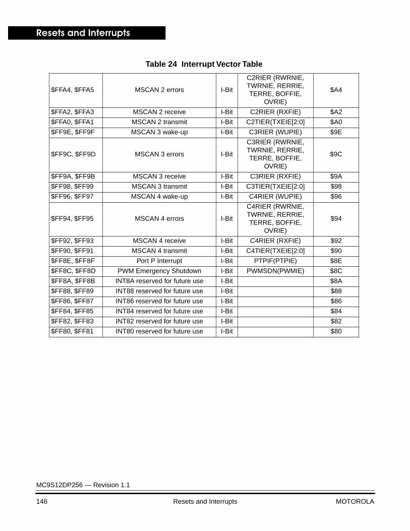
Resets and Interrupts
MC9S12DP256 — Revision 1.1
146 Resets and Interrupts MOTOROLA
$FFA4, $FFA5 MSCAN 2 errors I-Bit
C2RIER (RWRNIE, TWRNIE, RERRIE, TERRE, BOFFIE,
OVRIE)
$A4
$FFA2, $FFA3 MSCAN 2 receive I-Bit C2RIER (RXFIE) $A2
$FFA0, $FFA1 MSCAN 2 transmit I-Bit C2TIER(TXEIE[2:0] $A0
$FF9E, $FF9F MSCAN 3 wake-up I-Bit C3RIER (WUPIE) $9E
$FF9C, $FF9D MSCAN 3 errors I-Bit
C3RIER (RWRNIE, TWRNIE, RERRIE, TERRE, BOFFIE,
OVRIE)
$9C
$FF9A, $FF9B MSCAN 3 receive I-Bit C3RIER (RXFIE) $9A
$FF98, $FF99 MSCAN 3 transmit I-Bit C3TIER(TXEIE[2:0] $98
$FF96, $FF97 MSCAN 4 wake-up I-Bit C4RIER (WUPIE) $96
$FF94, $FF95 MSCAN 4 errors I-Bit
C4RIER (RWRNIE, TWRNIE, RERRIE, TERRE, BOFFIE,
OVRIE)
$94
$FF92, $FF93 MSCAN 4 receive I-Bit C4RIER (RXFIE) $92
$FF90, $FF91 MSCAN 4 transmit I-Bit C4TIER(TXEIE[2:0] $90
$FF8E, $FF8F Port P Interrupt I-Bit PTPIF(PTPIE) $8E
$FF8C, $FF8D PWM Emergency Shutdown I-Bit PWMSDN(PWMIE) $8C
$FF8A, $FF8B INT8A reserved for future use I-Bit $8A
$FF88, $FF89 INT88 reserved for future use I-Bit $88
$FF86, $FF87 INT86 reserved for future use I-Bit $86
$FF84, $FF85 INT84 reserved for future use I-Bit $84
$FF82, $FF83 INT82 reserved for future use I-Bit $82
$FF80, $FF81 INT80 reserved for future use I-Bit $80
Table 24 Interrupt Vector Table
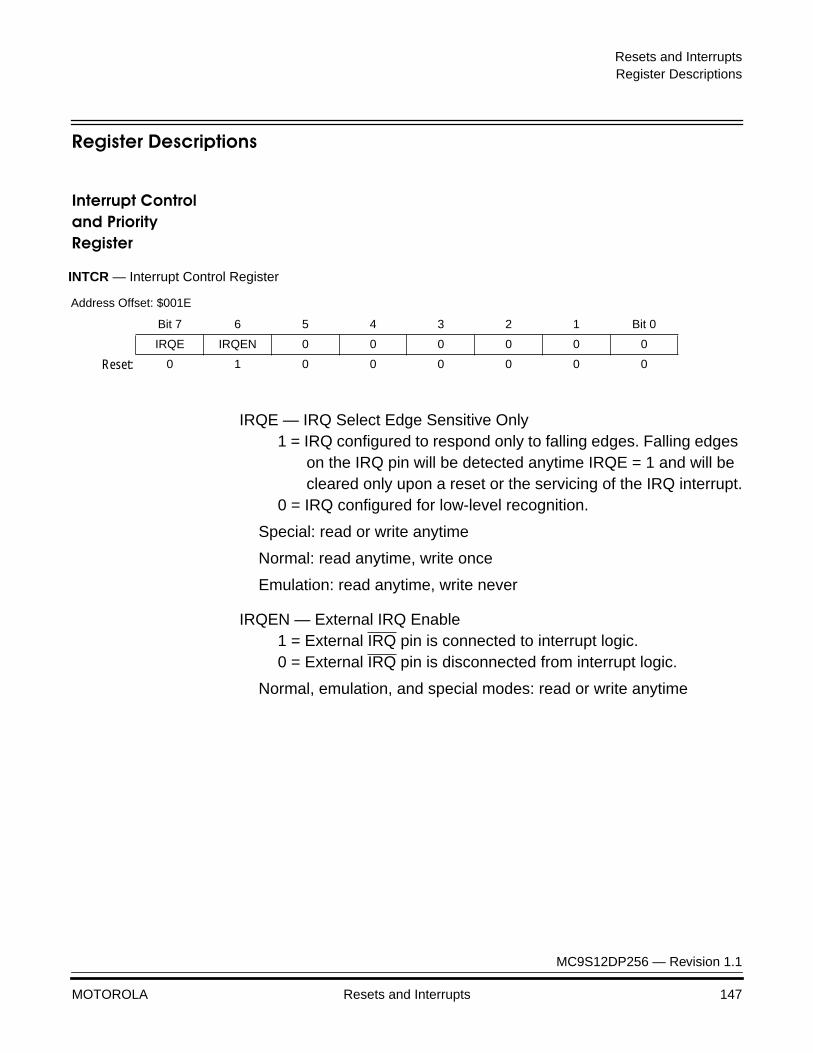
Resets and InterruptsRegister Descriptions
MC9S12DP256 — Revision 1.1
MOTOROLA Resets and Interrupts 147
Register Descriptions
Interrupt Control and Priority Register
IRQE — IRQ Select Edge Sensitive Only1 = IRQ configured to respond only to falling edges. Falling edges
on the IRQ pin will be detected anytime IRQE = 1 and will be cleared only upon a reset or the servicing of the IRQ interrupt.
0 = IRQ configured for low-level recognition.
Special: read or write anytime
Normal: read anytime, write once
Emulation: read anytime, write never
IRQEN — External IRQ Enable1 = External IRQ pin is connected to interrupt logic.0 = External IRQ pin is disconnected from interrupt logic.
Normal, emulation, and special modes: read or write anytime
INTCR — Interrupt Control Register
Address Offset: $001E
Bit 7 6 5 4 3 2 1 Bit 0
IRQE IRQEN 0 0 0 0 0 0
Reset: 0 1 0 0 0 0 0 0
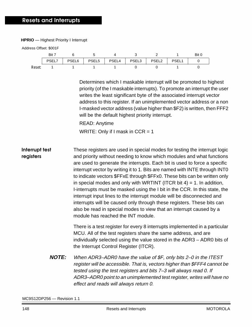
Resets and Interrupts
MC9S12DP256 — Revision 1.1
148 Resets and Interrupts MOTOROLA
Determines which I maskable interrupt will be promoted to highest priority (of the I maskable interrupts). To promote an interrupt the user writes the least significant byte of the associated interrupt vector address to this register. If an unimplemented vector address or a non I-masked vector address (value higher than $F2) is written, then FFF2 will be the default highest priority interrupt.
READ: Anytime
WRITE: Only if I mask in CCR = 1
Interrupt test registers
These registers are used in special modes for testing the interrupt logic and priority without needing to know which modules and what functions are used to generate the interrupts. Each bit is used to force a specific interrupt vector by writing it to 1. Bits are named with INTE through INT0 to indicate vectors $FFxE through $FFx0. These bits can be written only in special modes and only with WRTINT (ITCR bit 4) = 1. In addition, I-interrupts must be masked using the I bit in the CCR. In this state, the interrupt input lines to the interrupt module will be disconnected and interrupts will be caused only through these registers. These bits can also be read in special modes to view that an interrupt caused by a module has reached the INT module.
There is a test register for every 8 interrupts implemented in a particular MCU. All of the test registers share the same address, and are individually selected using the value stored in the ADR3 – ADR0 bits of the Interrupt Control Register (ITCR).
NOTE: When ADR3–ADR0 have the value of $F, only bits 2–0 in the ITEST register will be accessible. That is, vectors higher than $FFF4 cannot be tested using the test registers and bits 7–3 will always read 0. If ADR3–ADR0 point to an unimplemented test register, writes will have no effect and reads will always return 0.
HPRIO — Highest Priority I Interrupt
Address Offset: $001F
Bit 7 6 5 4 3 2 1 Bit 0
PSEL7 PSEL6 PSEL5 PSEL4 PSEL3 PSEL2 PSEL1 0
Reset: 1 1 1 1 0 0 1 0
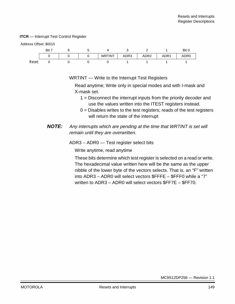
Resets and InterruptsRegister Descriptions
MC9S12DP256 — Revision 1.1
MOTOROLA Resets and Interrupts 149
WRTINT — Write to the Interrupt Test Registers
Read anytime; Write only in special modes and with I-mask and X-mask set.
1 = Disconnect the interrupt inputs from the priority decoder and use the values written into the ITEST registers instead.
0 = Disables writes to the test registers; reads of the test registers will return the state of the interrupt
NOTE: Any interrupts which are pending at the time that WRTINT is set will remain until they are overwritten.
ADR3 – ADR0 — Test register select bits
Write anytime, read anytime
These bits determine which test register is selected on a read or write. The hexadecimal value written here will be the same as the upper nibble of the lower byte of the vectors selects. That is, an “F” written into ADR3 – ADR0 will select vectors $FFFE – $FFF0 while a “7” written to ADR3 – ADR0 will select vectors $FF7E – $FF70.
ITCR — Interrupt Test Control Register
Address Offset: $0015
Bit 7 6 5 4 3 2 1 Bit 0
0 0 0 WRTINT ADR3 ADR2 ADR1 ADR0
Reset: 0 0 0 0 1 1 1 1
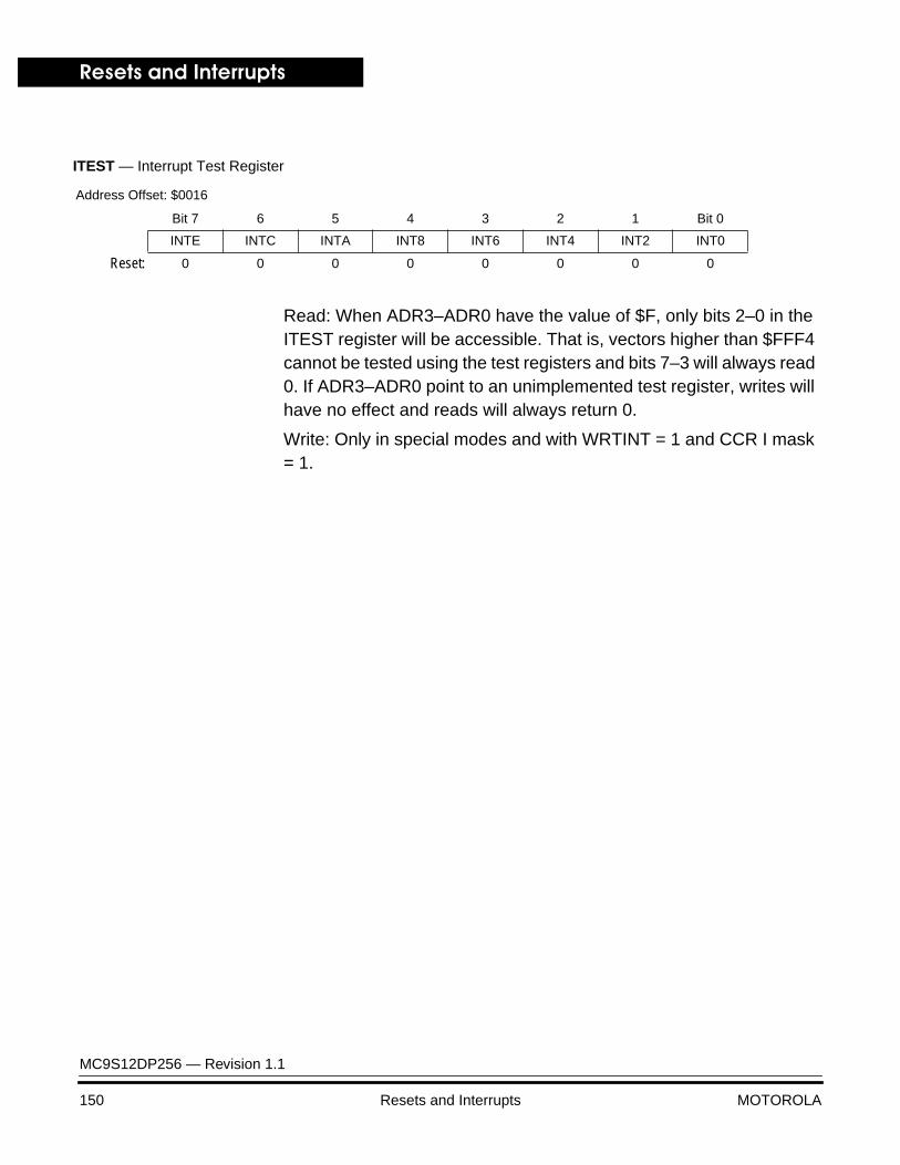
Resets and Interrupts
MC9S12DP256 — Revision 1.1
150 Resets and Interrupts MOTOROLA
Read: When ADR3–ADR0 have the value of $F, only bits 2–0 in the ITEST register will be accessible. That is, vectors higher than $FFF4 cannot be tested using the test registers and bits 7–3 will always read 0. If ADR3–ADR0 point to an unimplemented test register, writes will have no effect and reads will always return 0.
Write: Only in special modes and with WRTINT = 1 and CCR I mask = 1.
ITEST — Interrupt Test Register
Address Offset: $0016
Bit 7 6 5 4 3 2 1 Bit 0
INTE INTC INTA INT8 INT6 INT4 INT2 INT0
Reset: 0 0 0 0 0 0 0 0
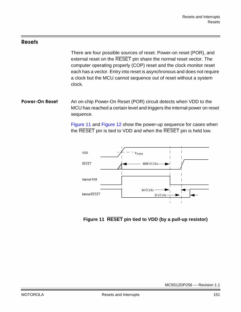
Resets and InterruptsResets
MC9S12DP256 — Revision 1.1
MOTOROLA Resets and Interrupts 151
Resets
There are four possible sources of reset. Power-on reset (POR), and external reset on the RESET pin share the normal reset vector. The computer operating properly (COP) reset and the clock monitor reset each has a vector. Entry into reset is asynchronous and does not require a clock but the MCU cannot sequence out of reset without a system clock.
Power-On Reset An on-chip Power-On Reset (POR) circuit detects when VDD to the MCU has reached a certain level and triggers the internal power on reset sequence.
Figure 11 and Figure 12 show the power-up sequence for cases when the RESET pin is tied to VDD and when the RESET pin is held low.
Figure 11 RESET pin tied to VDD (by a pull-up resistor)
VDD
RESET
Internal POR
4096 ECLKs
VPORR
64 ECLKs
32 ECLKsInternal RESET
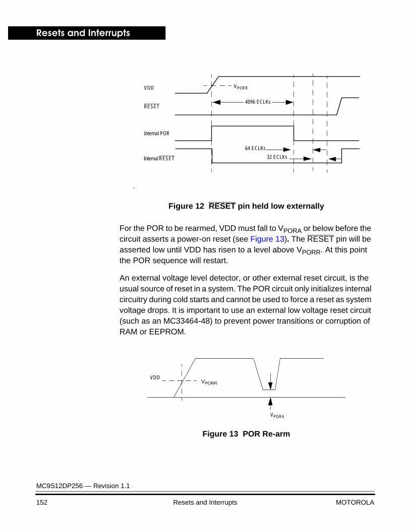
Resets and Interrupts
MC9S12DP256 — Revision 1.1
152 Resets and Interrupts MOTOROLA
Figure 12 RESET pin held low externally
For the POR to be rearmed, VDD must fall to VPORA or below before the circuit asserts a power-on reset (see Figure 13). The RESET pin will be asserted low until VDD has risen to a level above VPORR. At this point the POR sequence will restart.
An external voltage level detector, or other external reset circuit, is the usual source of reset in a system. The POR circuit only initializes internal circuitry during cold starts and cannot be used to force a reset as system voltage drops. It is important to use an external low voltage reset circuit (such as an MC33464-48) to prevent power transitions or corruption of RAM or EEPROM.
Figure 13 POR Re-arm
.
VPORR
4096 ECLKs
VDD
RESET
Internal POR
Internal RESET
64 ECLKs
32 ECLKs
VPORA
VDDVPORR
Resets and InterruptsResets
MC9S12DP256 — Revision 1.1
MOTOROLA Resets and Interrupts 153
External Reset External circuitry connected to the RESET pin should not include a large capacitance that would interfere with the ability of this signal to rise to a valid logic one within 32 ECLK cycles after the low drive is released. Upon detection of any reset, an internal circuit drives the RESET pin low and a clocked reset sequence controls when the MCU can begin normal processing.
NOTE: Entry into reset is asynchronous and does not require a clock. However, the MCU cannot sequence out of reset without a system clock.
In the case of POR or a clock monitor failure, a 4096 ECLK cycle oscillator startup delay is imposed before the reset recovery sequence starts (RESET is driven low throughout this 4096 cycle delay.) The internal reset recovery sequence then drives RESET low for 64 to 65 ECLK cycles and releases the drive to allow RESET to rise. 32 ECLK cycles later this circuit samples the RESET pin to see if it has risen to a logic one level. If RESET is low at this point, the reset is assumed to be coming from an external request and the internally latched states of the COP timeout and clock monitor failure are cleared so the normal reset vector ($FFFE:FFFF) is taken when RESET is finally released. If RESET is high after this 32 cycle delay, the reset source is tentatively assumed to be either a COP failure or a clock monitor failure. If the internally latched state of the clock monitor fail circuit is true, processing begins by fetching the clock monitor vector ($FFFC:FFFD). If no clock monitor failure is indicated, and the latched state of the COP timeout is true, processing begins by fetching the COP vector ($FFFA:FFFB). If neither clock monitor fail nor COP timeout are pending, processing begins by fetching the normal reset vector ($FFFE:FFFF).
COP Reset The COP watchdog enables the user to check that a program is running and sequencing properly. When the COP is being used, software is responsible for keeping a free running watchdog timer from timing out. If the watchdog timer times out it is an indication that the software is no longer being executed in the intended sequence; thus a system reset is initiated. Three control bits in the COPCTL register allow selection of seven COP time-out periods.
Resets and Interrupts
MC9S12DP256 — Revision 1.1
154 Resets and Interrupts MOTOROLA
When COP is enabled, the program must write $55 and $AA (in this order) to the ARMCOP register during the selected time-out period. Once this is done, the internal COP counter resets to the start of a new time-out period. If the program fails to do this the part will reset. Also, if any value other than $55 or $AA is written, the part is immediately reset.
Windowed COP operation is enabled by setting WCOP in the COPCTL register. In this mode, writes to the ARMCOP register must occur in the last 25% of the selected time-out period. A premature write will immediately reset the part.
To reset the internal COP counter to the start of a COP time-out period, set both the RTI rate select bits RTICTL[6:0] and the COP rate select bits COPCTL[2:0] to zero.
Clock Monitor Reset
If clock frequency falls below a predetermined limit when the clock monitor is enabled, a reset occurs.
The clock monitor circuit is based on an internal resistor-capacitor (RC) time delay. If no external clock edges are detected within this RC time delay, the clock monitor generates a system reset. The clock monitor function is enabled/disabled by the CME control bit in the PLLCTL register. This time-out is based on an RC delay so that the clock monitor can operate without any MCU clocks.
The input to the clock monitor is the reference clock (REFCLK.)

Resets and InterruptsEffects of Reset
MC9S12DP256 — Revision 1.1
MOTOROLA Resets and Interrupts 155
Effects of Reset
When a reset occurs, MCU registers and control bits are changed to known start-up states, as follows.
Operating Mode and Memory Map
Operating mode and default memory mapping are determined by the states of the BKGD, MODA, and MODB pins during reset. The MODA, MODB, and MODC bits in the MODE register reflect the status of the mode-select inputs at the rising edge of reset. Operating mode and default maps can subsequently be changed according to strictly defined rules.
Clock and Watchdog Control Logic
The COP watchdog system is enabled, with the CR[2:0] bits set for the longest duration time-out. The clock monitor is disabled. The RTIF flag is cleared and automatic hardware interrupts are masked. The rate control bits are cleared, and must be initialized before the RTI system is used.
Interrupts PSEL is initialized in the HPRIO register with the value $F2, causing the external IRQ pin to have the highest I-bit interrupt priority. The IRQ pin is configured for level-sensitive operation (for wired-OR systems). However, the interrupt mask bits in the CPU12 CCR are set to mask X- and I-related interrupt requests.
Parallel I/O If the MCU comes out of reset in a single-chip mode, all ports are configured as general-purpose high-impedance inputs.
If the MCU comes out of reset in an expanded mode, port A and port B are used for the address/data bus, and port E pins are normally used to control the external bus (operation of port E pins can be affected by the PEAR register). Out of reset, port K, port E, port H, port J, port M, port T, port S, port P, port ATD0 and port ATD1 are all configured as general-purpose inputs.
Resets and Interrupts
MC9S12DP256 — Revision 1.1
156 Resets and Interrupts MOTOROLA
Central Processing Unit
After reset, the CPU fetches a vector from the appropriate address, then begins executing instructions. The stack pointer and other CPU registers are indeterminate immediately after reset. The CCR X and I interrupt mask bits are set to mask any interrupt requests. The S bit is also set to inhibit the STOP instruction.
Memory After reset, the internal register block is located from $0000 to $03FF, RAM is at $1000 to $3FFF, and EEPROM is located at $0000 to $0FFF. In single chip mode one 16K byte FLASH EEPROM module is located from $4000 to $7FFF and $C000 to $FFFF, and the other sixteen 16K byte FLASH EEPROM modules are accessible through the program page window located from $8000 to $BFFF.
Other Resources The enhanced capture timer (ECT), pulse width modulation timer (PWM), serial communications interfaces (SCI0 and SCI1), serial peripheral interfaces (SPI0, SPI1 and SPI2), inter-IC bus (IIC), Byte Level Data Link Controller (BDLC), Motorola Scalable CANs (MSCAN0,.. MSCAN4), and analog-to-digital converters (ATD0 and ATD1) are off after reset.

Resets and InterruptsRegister Stacking
MC9S12DP256 — Revision 1.1
MOTOROLA Resets and Interrupts 157
Register Stacking
Once enabled, an interrupt request can be recognized at any time after the I bit in the CCR is cleared. When an interrupt service request is recognized, the CPU responds at the completion of the instruction being executed. Interrupt latency varies according to the number of cycles required to complete the instruction. Some of the longer instructions can be interrupted and will resume normally after servicing the interrupt.
When the CPU begins to service an interrupt, the instruction queue is cleared, the return address is calculated, and then it and the contents of the CPU registers are stacked as shown in Table 25.
After the CCR is stacked, the I bit (and the X bit, if an XIRQ interrupt service request is pending) is set to prevent other interrupts from disrupting the interrupt service routine. The interrupt vector for the highest priority source that was pending at the beginning of the interrupt sequence is fetched, and execution continues at the referenced location. At the end of the interrupt service routine, an RTI instruction restores the content of all registers from information on the stack, and normal program execution resumes.
If another interrupt is pending at the end of an interrupt service routine, the register unstacking and restacking is bypassed and the vector of the interrupt is fetched.
Table 25 Stacking Order on Entry to Interrupts
Memory Location CPU RegistersSP – 2 RTNH : RTNL SP – 4 YH : YL SP – 6 XH : XL SP – 8 B : A SP – 9 CCR

Resets and Interrupts
MC9S12DP256 — Revision 1.1
158 Resets and Interrupts MOTOROLA
MC9S12DP256 — Revision 1.1
MOTOROLA Voltage Regulator (VREG) 159
Voltage Regulator (VREG)Voltage Regulator (VREG)
Contents
Overview . . . . . . . . . . . . . . . . . . . . . . . . . . . . . . . . . . . . . . . . . . . . . . 159Features . . . . . . . . . . . . . . . . . . . . . . . . . . . . . . . . . . . . . . . . . . . . . . 159Block Diagram. . . . . . . . . . . . . . . . . . . . . . . . . . . . . . . . . . . . . . . . . . 160Functional Description. . . . . . . . . . . . . . . . . . . . . . . . . . . . . . . . . . . . 161External Pin Connection . . . . . . . . . . . . . . . . . . . . . . . . . . . . . . . . . . 161Reset Initialization . . . . . . . . . . . . . . . . . . . . . . . . . . . . . . . . . . . . . . . 164Modes of Operation. . . . . . . . . . . . . . . . . . . . . . . . . . . . . . . . . . . . . . 164
Overview
The voltage regulator (VREG) converts the external VDDR (5V±5%) supply to VDD and VDDPLL (2.5V ± 10%) used to supply the internal core logic as well as PLL and clock system.
Features
• Dual linear voltage regulator with nmos output transistors
• Standby mode to minimize power consumption
• Voltage reference derived from VDDA/VSSA
• Power on reset generator
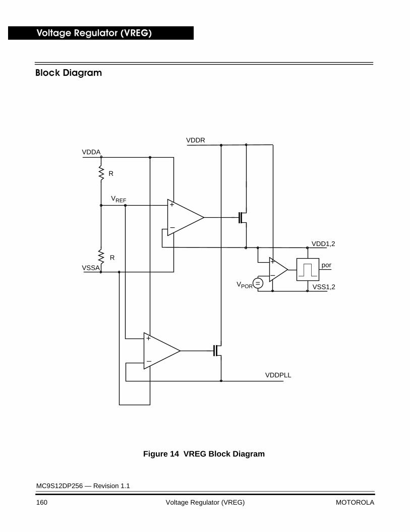
Voltage Regulator (VREG)
MC9S12DP256 — Revision 1.1
160 Voltage Regulator (VREG) MOTOROLA
Block Diagram
Figure 14 VREG Block Diagram
+
–
VDD1,2
VSS1,2
VDDPLL
VDDA
VSSA
VDDR
=
por+
–
+
–
R
R
VREF
VPOR
Voltage Regulator (VREG)Functional Description
MC9S12DP256 — Revision 1.1
MOTOROLA Voltage Regulator (VREG) 161
Functional Description
The voltage regulator module generates the supply voltage needed for the core logic as well as for the oscillator/pll section. The reference for the regulation loops are derived from a voltage divider connected between VDDA and VSSA. Both regulation loops, VDD and VDDPLL, consist of an operational amplifier driving an nmos power transistor in unit gain configuration. If there is no significant demand of output current (the CPU is in stop or pseudo stop mode) the voltage regulator is brought into standby mode, to decrease power consumption of the voltage regulator itself.
The voltage regulator can be enabled/disabled by the logic level on the VREGEN pin.
The level of VDD is internally monitored to generate a power on reset signal. If VDD is below VPORA reset will be asserted and a power on reset sequence will be triggered as soon as VDD rises above VPORR.
Change of VDDA or VSSA levels will directly influence the voltage levels at VDD and VDDPLL. Because of this reason, it is sufficient to monitor the level of VDDA externally to generate a system reset if the supply voltage is out of specification limits.
Please note VDDA, VDDR and VSSX are internally connected by anti parallel diodes.
External Pin Connection
The PCB must be carefully laid out to ensure proper operation of the voltage regulator as well as of the MCU itself. The following rules must be observed:
• Every supply pair must be decoupled by a ceramic capacitor connected as near as possible to the corresponding pins (C1 – C6).
• Central point of the ground star should be the VSSR pin.
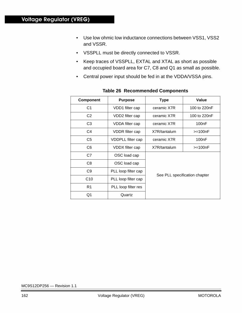
Voltage Regulator (VREG)
MC9S12DP256 — Revision 1.1
162 Voltage Regulator (VREG) MOTOROLA
• Use low ohmic low inductance connections between VSS1, VSS2 and VSSR.
• VSSPLL must be directly connected to VSSR.
• Keep traces of VSSPLL, EXTAL and XTAL as short as possible and occupied board area for C7, C8 and Q1 as small as possible.
• Central power input should be fed in at the VDDA/VSSA pins.
Table 26 Recommended Components
Component Purpose Type Value
C1 VDD1 filter cap ceramic X7R 100 to 220nF
C2 VDD2 filter cap ceramic X7R 100 to 220nF
C3 VDDA filter cap ceramic X7R 100nF
C4 VDDR filter cap X7R/tantalum >=100nF
C5 VDDPLL filter cap ceramic X7R 100nF
C6 VDDX filter cap X7R/tantalum >=100nF
C7 OSC load cap
See PLL specification chapter
C8 OSC load cap
C9 PLL loop filter cap
C10 PLL loop filter cap
R1 PLL loop filter res
Q1 Quartz
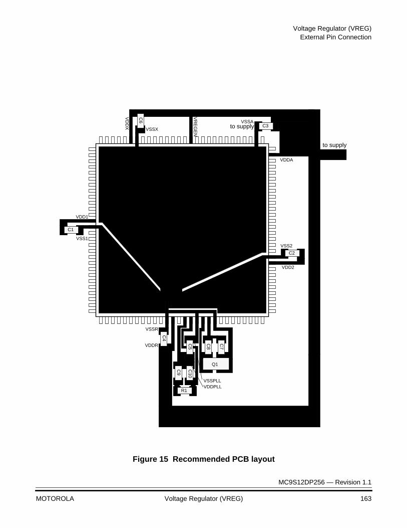
Voltage Regulator (VREG)External Pin Connection
MC9S12DP256 — Revision 1.1
MOTOROLA Voltage Regulator (VREG) 163
Figure 15 Recommended PCB layout
C5
C4
C1
C6
C3
C2
C8
C7
Q1
C10
C9
R1
VD
DX
VSSX
VDDR
VSSR
VDD1
VSS1
VDD2
VSS2
VDDPLLVSSPLL
VDDA
VSSA
VR
EG
EN
to supply
to supply
Voltage Regulator (VREG)
MC9S12DP256 — Revision 1.1
164 Voltage Regulator (VREG) MOTOROLA
Reset Initialization
On system power up, the voltage regulator is started in run mode if VREGEN is connected to VDDA. VDDA must be monitored by an external voltage comparator to ensure that the MCU is not executing code while the power supply is out of specification limits to avoid erroneous operation.
Modes of Operation
The voltage regulator has three operating modes: run, standby and disabled.
Normal Operation: Run
In run mode, both regulating loops of the voltage regulator are active. This mode is selected whenever the CPU is neither in stop nor in pseudo stop mode and VREGEN is externally connected to VDDA.
Special Operation: Standby
Standby mode is selected when the CPU is in stop or pseudo stop mode and VREGEN is externally connected to VDDA. In standby mode, the gates of the power transistors are directly connected to the reference voltage VREF ((VDDA - VSSA)/2), the loop amplifiers are switched off. In this case, the voltage regulator acts as a voltage clamp. In standby mode, the source resistance of the regulator is increased, but power consumption is significantly decreased.
Special Operation: Disabled
Shutdown mode can be selected by connecting VREGEN to VSSA. In this case, VDD and VDDPLL (2.5V±10%) must be supplied externally. In shutdown mode, VREG will also generate the power on reset signal.
MC9S12DP256 — Revision 1.1
MOTOROLA Flash EEPROM 256K 165
Flash EEPROM 256KFlash EEPROM 256K
Contents
Glossary . . . . . . . . . . . . . . . . . . . . . . . . . . . . . . . . . . . . . . . . . . . . . . 165Overview . . . . . . . . . . . . . . . . . . . . . . . . . . . . . . . . . . . . . . . . . . . . . . 166Features . . . . . . . . . . . . . . . . . . . . . . . . . . . . . . . . . . . . . . . . . . . . . . 167Block Diagram. . . . . . . . . . . . . . . . . . . . . . . . . . . . . . . . . . . . . . . . . . 168Module Memory Map . . . . . . . . . . . . . . . . . . . . . . . . . . . . . . . . . . . . 169Functional Description. . . . . . . . . . . . . . . . . . . . . . . . . . . . . . . . . . . . 174Register Descriptions . . . . . . . . . . . . . . . . . . . . . . . . . . . . . . . . . . . . 177External Pin Descriptions . . . . . . . . . . . . . . . . . . . . . . . . . . . . . . . . . 190Reset Initialization . . . . . . . . . . . . . . . . . . . . . . . . . . . . . . . . . . . . . . . 190Modes of Operation. . . . . . . . . . . . . . . . . . . . . . . . . . . . . . . . . . . . . . 190Low Power Options . . . . . . . . . . . . . . . . . . . . . . . . . . . . . . . . . . . . . . 190Interrupt Operation . . . . . . . . . . . . . . . . . . . . . . . . . . . . . . . . . . . . . . 191
Glossary
Flash Module Includes Bus Interface, Command Control, NVM BIST controller and four Flash blocks of 64K bytes each.
Flash Block 64K byte Flash macro organized as 32K by 16bit Words. Includes high voltage generation and parametric test features.
Flash Page 16K bytes of Flash located in address range $4000–$7FFF, $8000–$BFFF or $C000–$FFFF.
Erase Sector 512 bytes of Flash (8 rows of 32 words)
Flash EEPROM 256K
MC9S12DP256 — Revision 1.1
166 Flash EEPROM 256K MOTOROLA
Banked Register A register operating on one flash block which shares the same register address as the equivalent registers for the other flash blocks. The active register bank is selected by two bank-select bits in the unbanked register space.
Unbanked Register
A register which operates on all flash blocks.
Command Sequence
Three-step MCU instructions sequence to program or erase the Flash.
Overview
The 256K flash module is comprised of four 64K bytes blocks. They serve as electrically erasable and programmable, non-volatile program and data memory. The flash EEPROM is ideal for program and data storage for single-chip applications allowing for field reprogramming without requiring external programming voltage sources.
Each 64K byte flash block is arranged in a 32K by 16-bit configuration and may be read as either bytes, aligned words or misaligned words. Access time is one bus cycle for byte, and aligned word and two bus cycles for misaligned word read. Write operations for program or erase are only allowed as aligned word accesses. Each 64K block is organized in 1024 rows of 32 words. An erase sector contains 8 rows or 512 bytes. The erase mode supports erase sector as small as 512 bytes as well as mass erase of each 64K byte block. An erased word reads $FFFF and a programmed word reads $0000.
The programming voltage required to program and erase the flash is generated internally by on-chip charge pumps. Program and erase operations are performed by a command driven interface from the microcontroller using an internal state machine. All flash blocks can be programmed or erased at the same time, however it is not possible to read from a flash block while it is being erased or programmed.
Flash EEPROM 256KFeatures
MC9S12DP256 — Revision 1.1
MOTOROLA Flash EEPROM 256K 167
It is possible to perform ‘Read-While-Write’, i.e. program or erase one flash block under control of software routines executing out of another flash block.
Each block has hardware interlocks which protect data from accidental corruption. One protected area is located at the upper address of the flash module ($xxxx –$FFFF) normally used for boot code and another area is located at the lowest address ($4000–$xxxx). Two additional areas are located in the mapped memory pages $3A ($8000–$xxxx) and $3B ($xxxx–$BFFF).
Security information preventing intrusive access to the MCU is stored within the flash module.
Features
• 256K bytes of Flash made of four 64K byte blocks
– Single supply program and erase.
– Automated program and erase algorithm.
– Interrupt on command completion.
– All four flash blocks can be programmed and erased in parallel.
– Read-While-Write.
– Fast sector erase and word program operation.
– Flexible protection scheme against accidental program or erase.
– Security feature.
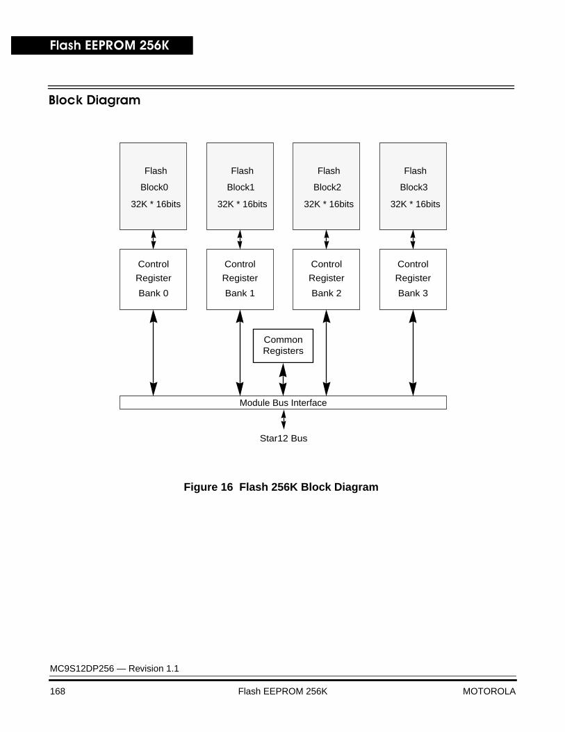
Flash EEPROM 256K
MC9S12DP256 — Revision 1.1
168 Flash EEPROM 256K MOTOROLA
Block Diagram
Figure 16 Flash 256K Block Diagram
Module Bus Interface
CommonRegisters
Star12 Bus
Flash
Block0
32K * 16bits
Flash
Block1
32K * 16bits
Flash
Block3
32K * 16bits
Flash
Block2
32K * 16bits
Control
Register
Bank 0
Control
Register
Bank 1
Control
Register
Bank 2
Control
Register
Bank 3
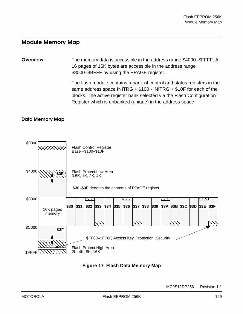
Flash EEPROM 256KModule Memory Map
MC9S12DP256 — Revision 1.1
MOTOROLA Flash EEPROM 256K 169
Module Memory Map
Overview The memory data is accessible in the address range $4000–$FFFF. All 16 pages of 16K bytes are accessible in the address range $8000–$BFFF by using the PPAGE register.
The flash module contains a bank of control and status registers in the same address space INITRG + $100 - INITRG + $10F for each of the blocks. The active register bank selected via the Flash Configuration Register which is unbanked (unique) in the address space
Data Memory Map
Figure 17 Flash Data Memory Map
16K pagedmemory
$0000Flash Control RegisterBase +$100–$10F
$4000
$8000
$C000
Flash Protect Low Area0.5K, 1K, 2K, 4K
Flash Protect High Area2K, 4K, 8K, 16K$FFFF
$FF00–$FF0F, Access Key, Protection, Security
$3F
$3E
$30–$3F denotes the contents of PPAGE register
$30 $35$34$32 $33 $36$31 $37$30 $30 $3D$3C$3A $3B $3E$39 $3F$38

Flash EEPROM 256K
MC9S12DP256 — Revision 1.1
170 Flash EEPROM 256K MOTOROLA
Figure 18 Flash Block Memory Maps and Paging
Flash 0Relative Address within Flash block
$0000
$4000
$8000
$C000
$FFFFFlash Protect High Area2K, 4K, 8K, 16K
Flash Protect Low Area0.5K, 1K, 2K, 4K
$FF00–$FF0F, Access Key
$3C
$3D
$3F
$3E
Protection, Security
Flash 1Relative Address within Flash Block
$0000
$4000
$8000
$C000
$FFFFFlash Protect High Area2K, 4K, 8K, 16K
Flash Protect Low Area0.5K, 1K, 2K, 4K
$38
$39
$3B
$3A
Flash 2Relative Address within Flash block
$0000
$4000
$8000
$C000
$FFFFFlash Protect High Area2K, 4K, 8K, 16K
Flash Protect Low Area0.5K, 1K, 2K, 4K
$34
$35
$37
$36
Flash 3Relative Address within Flash Block
$0000
$4000
$8000
$C000
$FFFFFlash Protect High Area2K, 4K, 8K, 16K
Flash Protect Low Area0.5K, 1K, 2K, 4K
$30
$31
$33
$32
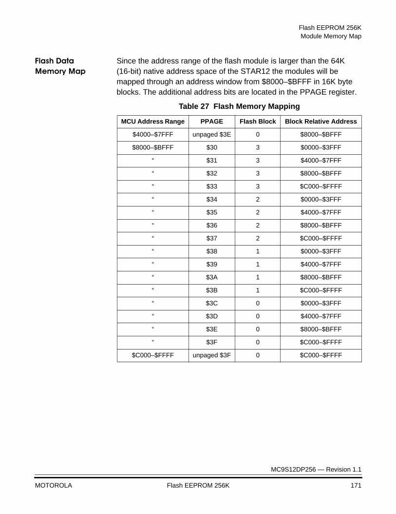
Flash EEPROM 256KModule Memory Map
MC9S12DP256 — Revision 1.1
MOTOROLA Flash EEPROM 256K 171
Flash Data Memory Map
Since the address range of the flash module is larger than the 64K (16-bit) native address space of the STAR12 the modules will be mapped through an address window from $8000–$BFFF in 16K byte blocks. The additional address bits are located in the PPAGE register.
Table 27 Flash Memory Mapping
MCU Address Range PPAGE Flash Block Block Relative Address
$4000–$7FFF unpaged $3E 0 $8000–$BFFF
$8000–$BFFF $30 3 $0000–$3FFF
“ $31 3 $4000–$7FFF
“ $32 3 $8000–$BFFF
“ $33 3 $C000–$FFFF
“ $34 2 $0000–$3FFF
“ $35 2 $4000–$7FFF
“ $36 2 $8000–$BFFF
“ $37 2 $C000–$FFFF
“ $38 1 $0000–$3FFF
“ $39 1 $4000–$7FFF
“ $3A 1 $8000–$BFFF
“ $3B 1 $C000–$FFFF
“ $3C 0 $0000–$3FFF
“ $3D 0 $4000–$7FFF
“ $3E 0 $8000–$BFFF
“ $3F 0 $C000–$FFFF
$C000–$FFFF unpaged $3F 0 $C000–$FFFF
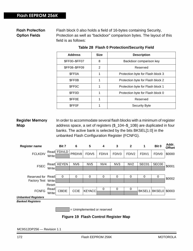
Flash EEPROM 256K
MC9S12DP256 — Revision 1.1
172 Flash EEPROM 256K MOTOROLA
Flash Protection Option Fields
Flash block 0 also holds a field of 16-bytes containing Security, Protection as well as “backdoor” comparison bytes. The layout of this field is as follows:
Register Memory Map
In order to accommodate several flash blocks with a minimum of register address space, a set of registers ($_104–$_10B) are duplicated in four banks. The active bank is selected by the bits BKSEL[1:0] in the unbanked Flash Configuration Register (FCNFG).
Table 28 Flash 0 Protection/Security Field
Address Size Description
$FF00–$FF07 8 Backdoor comparison key
$FF08–$FF09 2 Reserved
$FF0A 1 Protection byte for Flash block 3
$FF0B 1 Protection byte for Flash block 2
$FF0C 1 Protection byte for Flash block 1
$FF0D 1 Protection byte for Flash block 0
$FF0E 1 Reserved
$FF0F 1 Security Byte
Register name Bit 7 6 5 4 3 2 1 Bit 0 Addr.Offset
FCLKDIVRead: FDIVLD
PRDIV8 FDIV5 FDIV4 FDIV3 FDIV2 FDIV1 FDIV0 $0000Write:
FSECRead: KEYEN NV6 NV5 NV4 NV3 NV2 SEC01 SEC00
$0001Write:
Reserved forFactory Test
Read: 0 0 0 0 0 0 0 0$0002
Write:Reset:
FCNFGRead:
CBEIE CCIE KEYACC0 0 0
BKSEL1 BKSEL0 $0003Write:
Unbanked RegistersBanked Registers
= Unimplemented or reserved
Figure 19 Flash Control Register Map
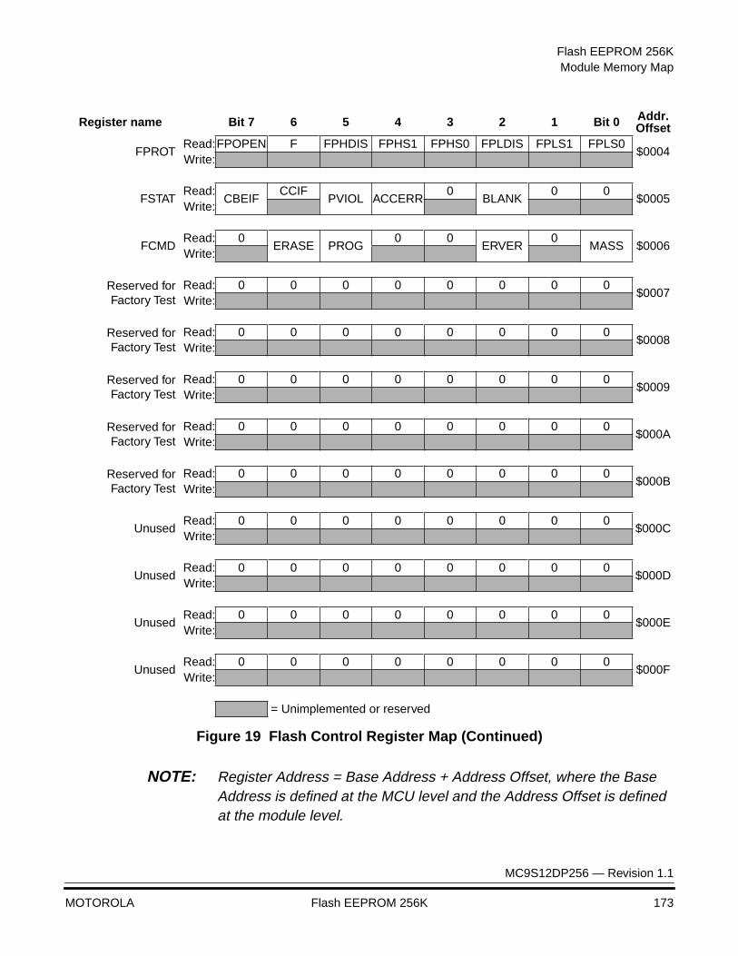
Flash EEPROM 256KModule Memory Map
MC9S12DP256 — Revision 1.1
MOTOROLA Flash EEPROM 256K 173
NOTE: Register Address = Base Address + Address Offset, where the Base Address is defined at the MCU level and the Address Offset is defined at the module level.
FPROTRead:FPOPEN F FPHDIS FPHS1 FPHS0 FPLDIS FPLS1 FPLS0
$0004Write:
FSTATRead:
CBEIFCCIF
PVIOL ACCERR0
BLANK0 0
$0005Write:
FCMDRead: 0
ERASE PROG0 0
ERVER0
MASS $0006Write:
Reserved forFactory Test
Read: 0 0 0 0 0 0 0 0$0007
Write:
Reserved forFactory Test
Read: 0 0 0 0 0 0 0 0$0008
Write:
Reserved forFactory Test
Read: 0 0 0 0 0 0 0 0$0009
Write:
Reserved forFactory Test
Read: 0 0 0 0 0 0 0 0$000A
Write:
Reserved forFactory Test
Read: 0 0 0 0 0 0 0 0$000B
Write:
UnusedRead: 0 0 0 0 0 0 0 0
$000CWrite:
UnusedRead: 0 0 0 0 0 0 0 0
$000DWrite:
UnusedRead: 0 0 0 0 0 0 0 0
$000EWrite:
UnusedRead: 0 0 0 0 0 0 0 0
$000FWrite:
Register name Bit 7 6 5 4 3 2 1 Bit 0 Addr.Offset
= Unimplemented or reserved
Figure 19 Flash Control Register Map (Continued)
Flash EEPROM 256K
MC9S12DP256 — Revision 1.1
174 Flash EEPROM 256K MOTOROLA
Functional Description
NOTE: All internal program and erase timings are handled by a state machine. The timebase is derived from the oscillator clock OSCCLK via a programmable down counter. The command register as well as the associated address and data registers operate as a buffer and a register (2-stage FIFO), so that a new command along with the necessary data and address can be stored to the buffers while the previous command is still in progress. Buffers empty condition as well as command completion are signalled by flags in the status register. Interrupts will be generated if enabled. The main reason for this approach is that the maximum high-voltage active time for a flash row is limited to tHV. Starting and stopping the high voltage after every word however would increase the programming time by a factor of two. The internal programming state machine will therefore keep the high voltage circuitry alive if a new program command operating on the same flash row (only address bits A[5:1] are allowed to change) is available, when the current program command is completed. The next programming cycle can then start without a delay. However if the command has changed, the address is not within the same row or the command buffer is empty, the high voltage will be turned off and restarted with the new command if required.
Program and Erase Procedures
Prior to issuing any program or erase commands it is necessary to program the FCLKDIV register to divide the oscillator clock to within the 150KHz to 200KHz range. Program and erase commands will not function if this register has not been initialized. See FCLKDIV register description for further details.
A Command State Machine, shared between all four flash blocks, is used to supervise the command sequence.
To prepare for a program or erase command sequence it is necessary to set the PPAGE and FCNFG registers as follows:
1. Write to bits BKSEL[1:0] in the FCNFG register to select the bank of registers associated with the 64K flash block to be programmed or erased (i.e. Flash 0, 1, 2 or 3) See Figure 17 for further details.
Flash EEPROM 256KFunctional Description
MC9S12DP256 — Revision 1.1
MOTOROLA Flash EEPROM 256K 175
2. Write to the (core) PPAGE register ($x030) to select one of the 16K page to be programmed if programming in the $8000–$BFFF address range. There is no need to set PPAGE when programming in the $4000–$7FFF or $C000–$FFFF address ranges.
After this initialization step the CBEIF flag should be tested to ensure that the address, data and command buffers are empty. If so, the command sequence can be started. The 3-step command sequence must be strictly adhered to and no intermediate writes to Flash registers are permitted between the 3 steps. The command sequence is as follows:
1. Write an aligned data word (16-bits) to be programmed to the flash address space between $4000 and $FFFF. The address and data will be stored in internal buffers. For program, all address bits are valid. For erase, the value of the data bytes is don’t care. For mass erase the address can be anywhere in the available address space of the 64K byte block to be erased. For sector erase the address bits 8:0 are don’t cared.
2. Write the program or erase command to the command buffer.
3. Reset CBEIF flag by writing a “1”. This will launch the command. The ACCERR and PVIOL flags should be tested to ensure the command sequence was valid. Five cycles after the CBEIF flag is cleared the CCIF flag will be cleared by hardware indicating that the command was successfully launched. The CBEIF flag will be set again indicating the address, data and command buffers are ready for a new command sequence to begin.
The completion of the command is indicated by the CCIF flag setting (Command Complete Interrupt Flag)
The Command State Machine will flag errors in program or erase sequences by means of the ACCERR (access error) and PVIOL (protection violation) flags in the FSTAT register. An erroneous command sequence will immediately abort and set the appropriate flag. The user has then to clear the ACCERR or PVIOL flags before being able to commence another command sequence.
The ACCERR flag will be set during the command sequence if any of the following illegal operations are performed. Such operations will cause the command sequence to immediately abort:
Flash EEPROM 256K
MC9S12DP256 — Revision 1.1
176 Flash EEPROM 256K MOTOROLA
1. Writing to the flash address space before initializing FCLKDIV.
2. Writing to the flash address space in the range $8000–$BFFF when PPAGE does not select a 16K block in the flash selected by BKSEL[1:0].
3. Writing to the flash address space $4000–$7FFF or $C000–$FFFF with BKSEL[1:0] not selecting Flash 0.
4. Writing a misaligned word or a byte to the flash address space.
5. Writing to the flash address space while CBEIF is not set.
6. Writing a second aligned word to the flash address space before executing a program or erase command on the previously written word.
7. Writing to any Flash register other than FCMD after writing an aligned word to the flash address space.
8. Writing a second command to the FCMD register before executing the previously written command.
9. Writing a MASS erase command to FCMD while any protection is enabled. See FPROT register description.
10. Writing a SECTOR erase command to FCMD while protection is enabled for that sector. See FPROT register description.
11. Writing to any Flash register other than FSTAT (to clear CBEIF) after writing to the command register.
12. Reading from the flash block while a command sequence is being entered or a program or erase command is being executed (i.e. CCIF not set). Such a read access returns non valid data. Any other block which is not being programmed can be read.
By writing a 0 to the CBEIF flag the command sequence can be aborted after the aligned word write to the flash address space or after writing a command to the FCMD register and before the command is launched.
The PVIOL flag will be set after the aligned write to the flash address space if an attempt to program or erase a protected area of the flash array is made. Such an operation will cause the command sequence to immediately abort. The user must clear the PVIOL flag before being able to commence another command sequence.
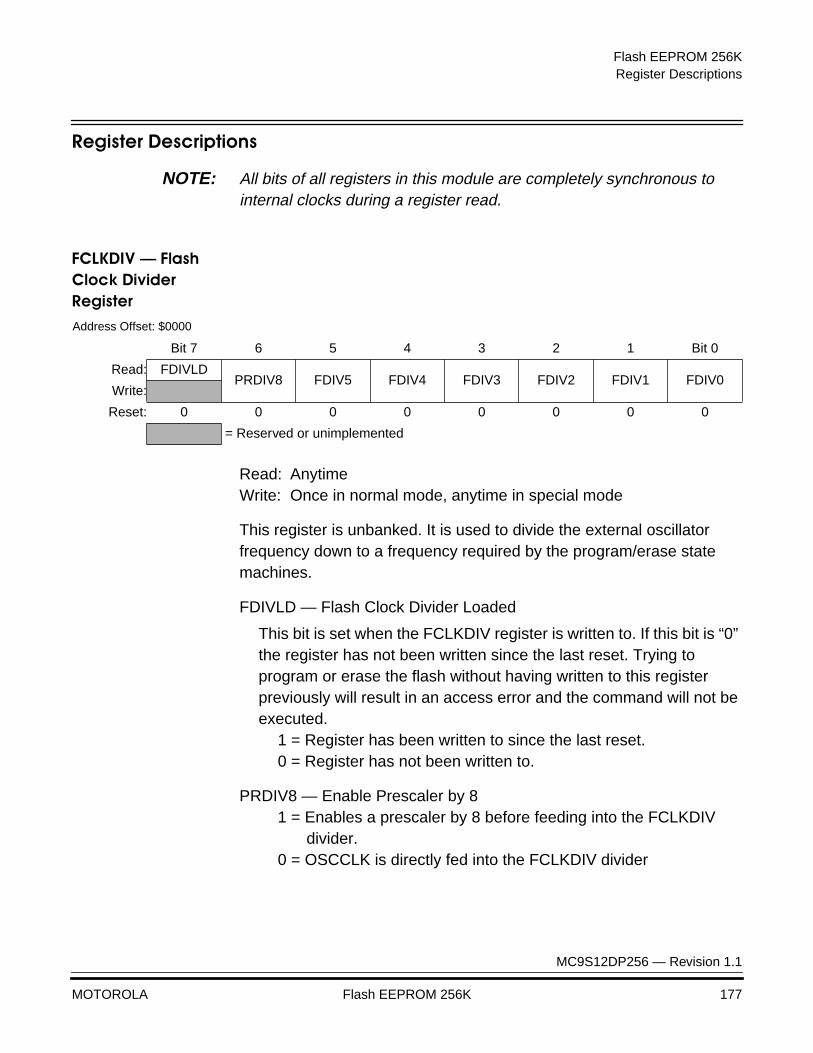
Flash EEPROM 256KRegister Descriptions
MC9S12DP256 — Revision 1.1
MOTOROLA Flash EEPROM 256K 177
Register Descriptions
NOTE: All bits of all registers in this module are completely synchronous to internal clocks during a register read.
FCLKDIV Ñ Flash Clock Divider Register
Read: AnytimeWrite: Once in normal mode, anytime in special mode
This register is unbanked. It is used to divide the external oscillator frequency down to a frequency required by the program/erase state machines.
FDIVLD — Flash Clock Divider Loaded
This bit is set when the FCLKDIV register is written to. If this bit is “0” the register has not been written since the last reset. Trying to program or erase the flash without having written to this register previously will result in an access error and the command will not be executed.
1 = Register has been written to since the last reset.0 = Register has not been written to.
PRDIV8 — Enable Prescaler by 81 = Enables a prescaler by 8 before feeding into the FCLKDIV
divider.0 = OSCCLK is directly fed into the FCLKDIV divider
Address Offset: $0000
Bit 7 6 5 4 3 2 1 Bit 0
Read: FDIVLDPRDIV8 FDIV5 FDIV4 FDIV3 FDIV2 FDIV1 FDIV0
Write:
Reset: 0 0 0 0 0 0 0 0
= Reserved or unimplemented
Flash EEPROM 256K
MC9S12DP256 — Revision 1.1
178 Flash EEPROM 256K MOTOROLA
FDIV[5:0] — Flash Clock Divider
The combination of FDIV8 and FDIV[5:0] is used to divide the oscillator clock down to a frequency of 150KHz - 200KHz. This resulting clock, FCLK, is used to drive the program and erase state machines for the flash.For frequencies of OSCCLK > 12.8MHz the Prescaler bit FDIV8 must be turned on.
FCLKDIV must be chosen such that the following equation is valid.
If FDIV8 == 1 then CLK = OSCCLK / 8, else CLK = OSCCLK
FCLKDIV = INT (CLK[KHz] / 200KHz)
The clock to the flash timing control is therefore:
FCLK = CLK / (FDIV[5:0] + 1)
150KHz < FCLK <= 200KHz
For example, if OSCCLK = 950KHz, FCLKDIV should be set to 4 and FDIV8 set to 0. The resulting FCLK is 190KHz. As a result the flash timings are increased by:
(200 - 190) / 200 x 100% = 5%
Remark: INT means rounding towards 0. Example: INT(950KHz/200KHz) = 4.
WARNING: Programming the flash with OSCCLK < 500KHz should be avoided. Setting FCLKDIV to a value such that FCLK < 150KHz can destroy the flash due to overstress. Setting FCLKDIV to a value such that FCLK > 200KHz can result in improperly programmed memory cells.
NOTE: Command execution time will increase proportionally with the period of FCLK.
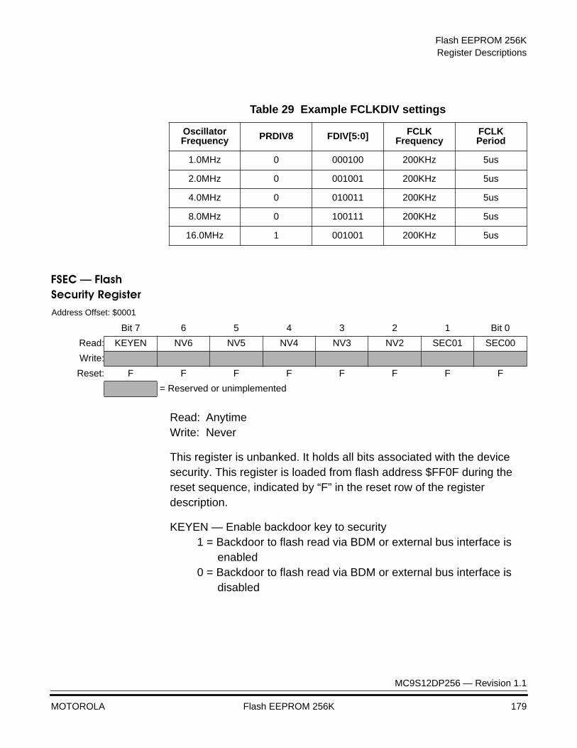
Flash EEPROM 256KRegister Descriptions
MC9S12DP256 — Revision 1.1
MOTOROLA Flash EEPROM 256K 179
FSEC Ñ Flash Security Register
Read: AnytimeWrite: Never
This register is unbanked. It holds all bits associated with the device security. This register is loaded from flash address $FF0F during the reset sequence, indicated by “F” in the reset row of the register description.
KEYEN — Enable backdoor key to security1 = Backdoor to flash read via BDM or external bus interface is
enabled0 = Backdoor to flash read via BDM or external bus interface is
disabled
Table 29 Example FCLKDIV settings
Oscillator Frequency PRDIV8 FDIV[5:0] FCLK
FrequencyFCLKPeriod
1.0MHz 0 000100 200KHz 5us
2.0MHz 0 001001 200KHz 5us
4.0MHz 0 010011 200KHz 5us
8.0MHz 0 100111 200KHz 5us
16.0MHz 1 001001 200KHz 5us
Address Offset: $0001
Bit 7 6 5 4 3 2 1 Bit 0
Read: KEYEN NV6 NV5 NV4 NV3 NV2 SEC01 SEC00
Write:
Reset: F F F F F F F F
= Reserved or unimplemented
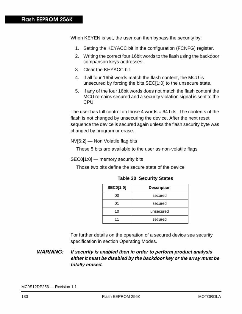
Flash EEPROM 256K
MC9S12DP256 — Revision 1.1
180 Flash EEPROM 256K MOTOROLA
When KEYEN is set, the user can then bypass the security by:
1. Setting the KEYACC bit in the configuration (FCNFG) register.
2. Writing the correct four 16bit words to the flash using the backdoor comparison keys addresses.
3. Clear the KEYACC bit.
4. If all four 16bit words match the flash content, the MCU is unsecured by forcing the bits SEC[1:0] to the unsecure state.
5. If any of the four 16bit words does not match the flash content the MCU remains secured and a security violation signal is sent to the CPU.
The user has full control on those 4 words = 64 bits. The contents of the flash is not changed by unsecuring the device. After the next reset sequence the device is secured again unless the flash security byte was changed by program or erase.
NV[6:2] — Non Volatile flag bits
These 5 bits are available to the user as non-volatile flags
SEC0[1:0] — memory security bits
Those two bits define the secure state of the device
For further details on the operation of a secured device see security specification in section Operating Modes.
WARNING: If security is enabled then in order to perform product analysis either it must be disabled by the backdoor key or the array must be totally erased.
Table 30 Security States
SEC0[1:0] Description
00 secured
01 secured
10 unsecured
11 secured
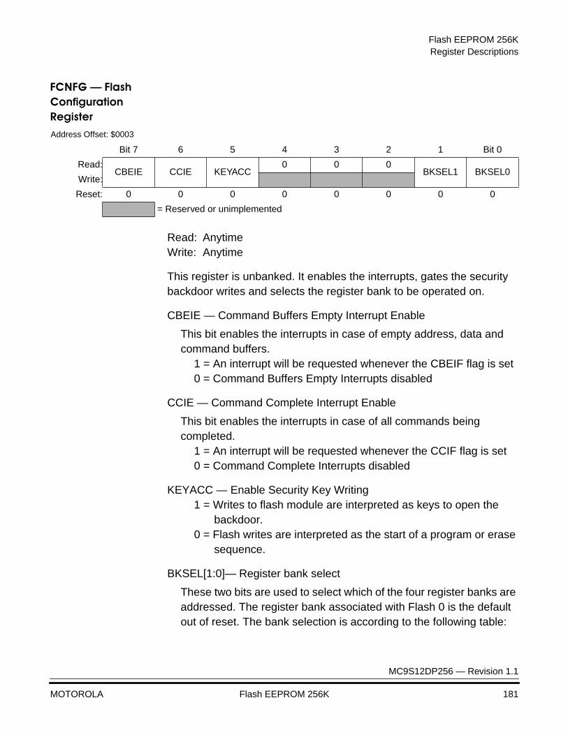
Flash EEPROM 256KRegister Descriptions
MC9S12DP256 — Revision 1.1
MOTOROLA Flash EEPROM 256K 181
FCNFG Ñ Flash Configuration Register
Read: AnytimeWrite: Anytime
This register is unbanked. It enables the interrupts, gates the security backdoor writes and selects the register bank to be operated on.
CBEIE — Command Buffers Empty Interrupt Enable
This bit enables the interrupts in case of empty address, data and command buffers.
1 = An interrupt will be requested whenever the CBEIF flag is set0 = Command Buffers Empty Interrupts disabled
CCIE — Command Complete Interrupt Enable
This bit enables the interrupts in case of all commands being completed.
1 = An interrupt will be requested whenever the CCIF flag is set0 = Command Complete Interrupts disabled
KEYACC — Enable Security Key Writing1 = Writes to flash module are interpreted as keys to open the
backdoor.0 = Flash writes are interpreted as the start of a program or erase
sequence.
BKSEL[1:0]— Register bank select
These two bits are used to select which of the four register banks are addressed. The register bank associated with Flash 0 is the default out of reset. The bank selection is according to the following table:
Address Offset: $0003
Bit 7 6 5 4 3 2 1 Bit 0
Read:CBEIE CCIE KEYACC
0 0 0BKSEL1 BKSEL0
Write:
Reset: 0 0 0 0 0 0 0 0
= Reserved or unimplemented
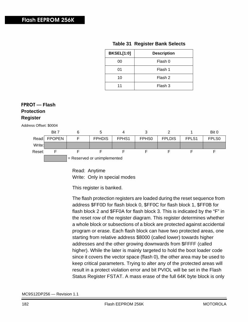
Flash EEPROM 256K
MC9S12DP256 — Revision 1.1
182 Flash EEPROM 256K MOTOROLA
FPROT Ñ Flash Protection Register
Read: AnytimeWrite: Only in special modes
This register is banked.
The flash protection registers are loaded during the reset sequence from address $FF0D for flash block 0, $FF0C for flash block 1, $FF0B for flash block 2 and $FF0A for flash block 3. This is indicated by the “F” in the reset row of the register diagram. This register determines whether a whole block or subsections of a block are protected against accidental program or erase. Each flash block can have two protected areas, one starting from relative address $8000 (called lower) towards higher addresses and the other growing downwards from $FFFF (called higher). While the later is mainly targeted to hold the boot loader code since it covers the vector space (flash 0), the other area may be used to keep critical parameters. Trying to alter any of the protected areas will result in a protect violation error and bit PVIOL will be set in the Flash Status Register FSTAT. A mass erase of the full 64K byte block is only
Table 31 Register Bank Selects
BKSEL[1:0] Description
00 Flash 0
01 Flash 1
10 Flash 2
11 Flash 3
Address Offset: $0004
Bit 7 6 5 4 3 2 1 Bit 0
Read: FPOPEN F FPHDIS FPHS1 FPHS0 FPLDIS FPLS1 FPLS0
Write:
Reset: F F F F F F F F
= Reserved or unimplemented

Flash EEPROM 256KRegister Descriptions
MC9S12DP256 — Revision 1.1
MOTOROLA Flash EEPROM 256K 183
possible when protection is fully disabled by setting the FPLDIS and FPHDIS bits.
In order to change the flash protection in special modes, the protection register can be written directly.
In order to change the protection in user mode the flash locations $FF0A, $FF0B, $FF0C and $FF0D have to be re-programmed and the MCU reset to reload the FPROT registers from those flash locations.
The size of the protected ranges for the lower and higher subsections are determined by FPHS1, FPHS0 and FPLS1, FPLS0 respectively. The protections are disabled by the bits FPHDIS and FPLDIS respectively.
FPOPEN — Opens the flash block or subsections of it for program or erase.
1 = The flash block or subsections are enabled to program or erase.
0 = The whole flash block is protected. In this case the other bits within the protect register are don’t care.
FPHDIS — Flash Protection Higher address range disableThis bit determines whether there is a protected area at the higher end of the flash block address map.
1 = Protection disabled0 = Protection enabled
FPHS[1:0] — Flash Protection Higher address sizeThese 2 bits determine the size of the protected area.
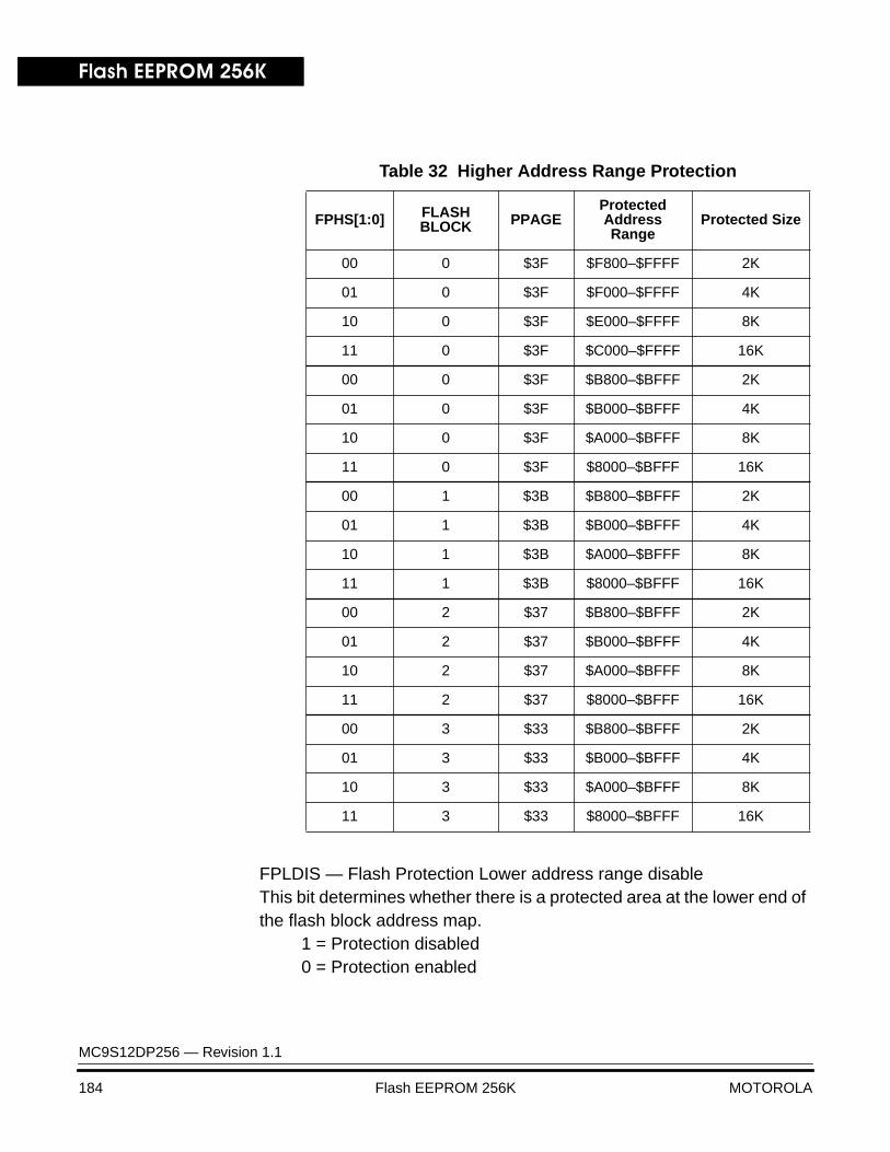
Flash EEPROM 256K
MC9S12DP256 — Revision 1.1
184 Flash EEPROM 256K MOTOROLA
FPLDIS — Flash Protection Lower address range disableThis bit determines whether there is a protected area at the lower end of the flash block address map.
1 = Protection disabled0 = Protection enabled
Table 32 Higher Address Range Protection
FPHS[1:0] FLASHBLOCK PPAGE
Protected Address Range
Protected Size
00 0 $3F $F800–$FFFF 2K
01 0 $3F $F000–$FFFF 4K
10 0 $3F $E000–$FFFF 8K
11 0 $3F $C000–$FFFF 16K
00 0 $3F $B800–$BFFF 2K
01 0 $3F $B000–$BFFF 4K
10 0 $3F $A000–$BFFF 8K
11 0 $3F $8000–$BFFF 16K
00 1 $3B $B800–$BFFF 2K
01 1 $3B $B000–$BFFF 4K
10 1 $3B $A000–$BFFF 8K
11 1 $3B $8000–$BFFF 16K
00 2 $37 $B800–$BFFF 2K
01 2 $37 $B000–$BFFF 4K
10 2 $37 $A000–$BFFF 8K
11 2 $37 $8000–$BFFF 16K
00 3 $33 $B800–$BFFF 2K
01 3 $33 $B000–$BFFF 4K
10 3 $33 $A000–$BFFF 8K
11 3 $33 $8000–$BFFF 16K
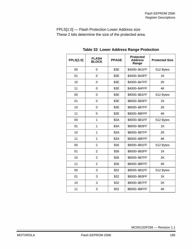
Flash EEPROM 256KRegister Descriptions
MC9S12DP256 — Revision 1.1
MOTOROLA Flash EEPROM 256K 185
FPLS[1:0] — Flash Protection Lower Address sizeThese 2 bits determine the size of the protected area.
Table 33 Lower Address Range Protection
FPLS[1:0] FLASH BLOCK PPAGE
Protected Address Range
Protected Size
00 0 $3E $4000–$41FF 512 Bytes
01 0 $3E $4000–$43FF 1K
10 0 $3E $4000–$47FF 2K
11 0 $3E $4000–$4FFF 4K
00 0 $3E $8000–$81FF 512 Bytes
01 0 $3E $8000–$83FF 1K
10 0 $3E $8000–$87FF 2K
11 0 $3E $8000–$8FFF 4K
00 1 $3A $8000–$81FF 512 Bytes
01 1 $3A $8000–$83FF 1K
10 1 $3A $8000–$87FF 2K
11 1 $3A $8000–$8FFF 4K
00 2 $36 $8000–$81FF 512 Bytes
01 2 $36 $8000–$83FF 1K
10 2 $36 $8000–$87FF 2K
11 2 $36 $8000–$8FFF 4K
00 3 $32 $8000–$81FF 512 Bytes
01 3 $32 $8000–$83FF 1K
10 3 $32 $8000–$87FF 2K
11 3 $32 $8000–$8FFF 4K

Flash EEPROM 256K
MC9S12DP256 — Revision 1.1
186 Flash EEPROM 256K MOTOROLA
FSTAT Ñ Flash Status Register
Read: AnytimeWrite: Anytime to clear flags
This register is banked. The bits in this register are set by various conditions.
CBEIF — Command Buffers Empty Interrupt Flag
Indicates that the address, data and command buffers are empty so that a new command sequence can be started. The flag is cleared by writing a “1”. By clearing the flag the command sequence is launched. Writing a “0” aborts a command sequence that has not yet been launched and sets the ACCERR flag.
1 = Buffers are ready to accept a new command.0 = Buffers are full.
CCIF — Command Complete Interrupt Flag
Indicates that there are no more commands pending. The flag is cleared by hardware. Writing has no effect.
1 = All commands are completed0 = Command in progress
PVIOL — Protection violation
Indicates an attempt was made to program or erase an address in a protected memory area. A subsequent program or erase command cannot executed while this flag is set. The flag is cleared by writing a “1”. Writing a “0” has no effect. The flag is also cleared by writing a new, valid command after CBEIF is cleared or when CCIF is clear.
1 = A protection violation has occurred.0 = no failure
Address Offset: $0005
Bit 7 6 5 4 3 2 1 Bit 0
Read:CBEIF
CCIFPVIOL ACCERR
0BLANK
0 0
Write:
Reset: 1 1 0 0 0 0 0 0
= Reserved or unimplemented

Flash EEPROM 256KRegister Descriptions
MC9S12DP256 — Revision 1.1
MOTOROLA Flash EEPROM 256K 187
ACCERR — Access error
Indicates an illegal access to the flash block or violation of the defined command sequence. This can be:
1. Writing to the flash address space before initializing FCLKDIV.
2. Writing to the flash address space in the range $8000–$BFFF when PPAGE does not select a 16K block in the flash selected by BKSEL[1:0].
3. Writing to the flash address space $4000–$7FFF or $C000–$FFFF with BKSEL[1:0] not selecting Flash 0.
4. Writing a misaligned word or a byte to the flash address space.
5. Writing to the flash address space while CBEIF is not set.
6. Writing a second aligned word to the flash address space before executing a program or erase command on the previously written word.
7. Writing to any Flash register other than FCMD after writing an aligned word to the flash address space.
8. Writing a second command to the FCMD register before executing the previously written command.
9. Writing a MASS erase command to FCMD while any protection is enabled. See FPROT register description.
10. Writing a SECTOR erase command to FCMD while protection is enabled for that sector. See FPROT register description.
11. Writing to any Flash register other than FSTAT (to clear CBEIF) after writing to the command register.
12. Reading from the flash block while a command sequence is being entered or a program or erase command is being executed. (i.e. CCIF not set). Such a read access returns non valid data
13. The part enters STOP mode and a program or erase command is in progress. The command is aborted.
The flag is cleared by writing a “1”. Writing a “0” has no effect.1 = Access error has occurred.0 = Command sequence or command execution successfully
completed.

Flash EEPROM 256K
MC9S12DP256 — Revision 1.1
188 Flash EEPROM 256K MOTOROLA
BLANK — Blank Verify Flag
Indicates that the flash block is fully erased in response to an Erase- Verify command. The flag is cleared by writing a “1”. Writing a “0” has no effect.
1 = Flash block fully erased.0 = Flash block not fully erased.
BITS[1:0] — These bits are reserved for factory testing and are not available to the user.
FCMD Ñ Flash Command Buffer and Register
Read: AnytimeWrite: After aligned write to the flash address space in the command
sequence. (See PVIOL description in FSTAT register)
This register is banked and buffered.
ERASE — Erase flash
Erases a flash sector (512 bytes) or the whole flash depending on the MASS bit. Trying to erase a sector located in a protected area will result in a protection violation indicated by the PVIOL bit in the FSTAT register being set.
1 = Perform a sector erase if MASS=0 or a mass erase if MASS=1.0 = -
Address Offset: $0006
Bit 7 6 5 4 3 2 1 Bit 0
Read: 0ERASE PROG
0 0ERVER
0MASS
Write:
Reset: 0 0 0 0 0 0 0 0
= Reserved or unimplemented
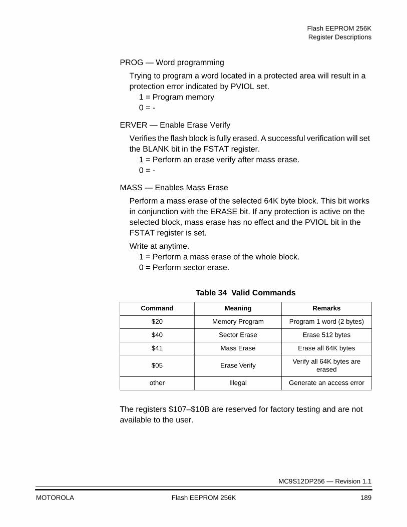
Flash EEPROM 256KRegister Descriptions
MC9S12DP256 — Revision 1.1
MOTOROLA Flash EEPROM 256K 189
PROG — Word programming
Trying to program a word located in a protected area will result in a protection error indicated by PVIOL set.
1 = Program memory0 = -
ERVER — Enable Erase Verify
Verifies the flash block is fully erased. A successful verification will set the BLANK bit in the FSTAT register.
1 = Perform an erase verify after mass erase.0 = -
MASS — Enables Mass Erase
Perform a mass erase of the selected 64K byte block. This bit works in conjunction with the ERASE bit. If any protection is active on the selected block, mass erase has no effect and the PVIOL bit in the FSTAT register is set.
Write at anytime.1 = Perform a mass erase of the whole block.0 = Perform sector erase.
The registers $107–$10B are reserved for factory testing and are not available to the user.
Table 34 Valid Commands
Command Meaning Remarks
$20 Memory Program Program 1 word (2 bytes)
$40 Sector Erase Erase 512 bytes
$41 Mass Erase Erase all 64K bytes
$05 Erase VerifyVerify all 64K bytes are
erased
other Illegal Generate an access error
Flash EEPROM 256K
MC9S12DP256 — Revision 1.1
190 Flash EEPROM 256K MOTOROLA
External Pin Descriptions
This module does not have external pins relevant for the user.
Reset Initialization
Out of reset the module holds core activity while the Protection and Security registers are loaded from Flash 0. Thereafter, the Flash module is immediately accessible, operating in read mode.
If a reset occurs while any command is in progress that command will be immediately aborted. The state of the word being programmed or the sector / block being erased is not guaranteed.
Modes of Operation
Security Modes The flash module provides the necessary security information to the rest of the chip. This information is stored within a byte in the flash block 0 ($FF0F). This byte is read automatically after each reset and stored in a volatile register. This information also protects the flash module from intrusive reads via the external bus interface or the BDM mode. The customer however can disable the security by providing a 64 bit key.
Low Power Options
When the array or the registers are not being accessed clocking to the register block is shut off to save power. The only exceptions to this are the flag bits in the FSTAT registers which are updated by internal state machines.
Run Mode No special current saving modes available.
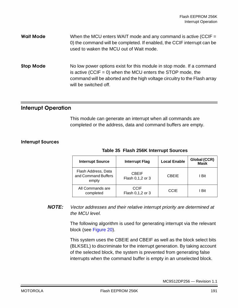
Flash EEPROM 256KInterrupt Operation
MC9S12DP256 — Revision 1.1
MOTOROLA Flash EEPROM 256K 191
Wait Mode When the MCU enters WAIT mode and any command is active (CCIF = 0) the command will be completed. If enabled, the CCIF interrupt can be used to waken the MCU out of Wait mode.
Stop Mode No low power options exist for this module in stop mode. If a command is active (CCIF = 0) when the MCU enters the STOP mode, the command will be aborted and the high voltage circuitry to the Flash array will be switched off.
Interrupt Operation
This module can generate an interrupt when all commands are completed or the address, data and command buffers are empty.
Interrupt Sources
NOTE: Vector addresses and their relative interrupt priority are determined at the MCU level.
The following algorithm is used for generating interrupt via the relevant block (see Figure 20).
This system uses the CBEIE and CBEIF as well as the block select bits (BLKSEL) to discriminate for the interrupt generation. By taking account of the selected block, the system is prevented from generating false interrupts when the command buffer is empty in an unselected block.
Table 35 Flash 256K Interrupt Sources
Interrupt Source Interrupt Flag Local Enable Global (CCR) Mask
Flash Address, Data and Command Buffers
empty
CBEIFFlash 0,1,2 or 3
CBEIE I Bit
All Commands are completed
CCIFFlash 0,1,2 or 3
CCIE I Bit
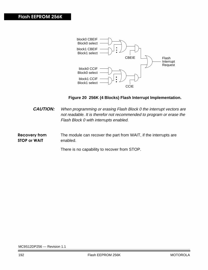
Flash EEPROM 256K
MC9S12DP256 — Revision 1.1
192 Flash EEPROM 256K MOTOROLA
Figure 20 256K (4 Blocks) Flash Interrupt Implementation.
CAUTION: When programming or erasing Flash Block 0 the interrupt vectors are not readable. It is therefor not recommended to program or erase the Flash Block 0 with interrupts enabled.
Recovery from STOP or WAIT
The module can recover the part from WAIT, if the interrupts are enabled.
There is no capability to recover from STOP.
block0 CBEIFBlock0 select
block1 CBEIFBlock1 select
block0 CCIFBlock0 select
block1 CCIFBlock1 select
CBEIE
CCIE
FlashInterruptRequest
MC9S12DP256 — Revision 1.1
MOTOROLA EEPROM 4K 193
EEPROM 4KEEPROM 4K
Contents
Glossary . . . . . . . . . . . . . . . . . . . . . . . . . . . . . . . . . . . . . . . . . . . . . . 193Overview . . . . . . . . . . . . . . . . . . . . . . . . . . . . . . . . . . . . . . . . . . . . . . 194Features . . . . . . . . . . . . . . . . . . . . . . . . . . . . . . . . . . . . . . . . . . . . . . 194Block Diagram. . . . . . . . . . . . . . . . . . . . . . . . . . . . . . . . . . . . . . . . . . 195Module Memory Map . . . . . . . . . . . . . . . . . . . . . . . . . . . . . . . . . . . . 195Functional Description. . . . . . . . . . . . . . . . . . . . . . . . . . . . . . . . . . . . 198Register Descriptions . . . . . . . . . . . . . . . . . . . . . . . . . . . . . . . . . . . . 201External Pin Descriptions . . . . . . . . . . . . . . . . . . . . . . . . . . . . . . . . . 210Reset Initialization . . . . . . . . . . . . . . . . . . . . . . . . . . . . . . . . . . . . . . . 210Modes of Operation. . . . . . . . . . . . . . . . . . . . . . . . . . . . . . . . . . . . . . 210Interrupt Operation . . . . . . . . . . . . . . . . . . . . . . . . . . . . . . . . . . . . . . 211
Glossary
EEPROM Module Includes Bus Interface, Command Control, NVM BIST controller and a 4k byte EEPROM block.
EEPROM Block 4K byte EEPROM macro organized as 2048 by 16bit Words including high voltage generation and parametric test features.
Erase Sector 4 bytes (2 words)
Command Sequence
Three-step MCU instructions sequence to program or erase the Flash.

EEPROM 4K
MC9S12DP256 — Revision 1.1
194 EEPROM 4K MOTOROLA
Overview
The 4k byte EEPROM module serves as electrically erasable and programmable, non-volatile data memory without requiring external programming voltage sources.
The EEPROM may be read as either bytes, aligned words or misaligned words. Access time is one bus cycle for byte and aligned word and two bus cycles for misaligned word read. Write operations for program or erase are only allowed as aligned word accesses. The 4k byte array is organized in 2048 rows of 2 bytes. An erase sector contains 2 rows. The erase mode supports erase sector of 4 bytes as well as a mass erase of the entire 4k byte block.
The programming voltage required to program and erase the EEPROM is generated internally by on-chip charge pumps. Program and erase operations are performed by a command driven interface from the microcontroller using an internal state machine. It is not possible to read from the EEPROM block while it is being erased or programmed.
The EEPROM has hardware interlocks which protect data from accidental corruption. The protected area is located at the upper address end of the EEPROM module ($xxxx – $xFFF). The size of the protected area can be set from 0 to 512 bytes in multiples of 64 bytes and grows downwards from address $xFFF.
Features
• 4k bytes of EEPROM
– Single supply program and erase.
– Automated program and erase algorithm.
– Interrupt on command completion.
– Fast sector erase and word program operation.
– Flexible protection scheme against accidental program or erase.
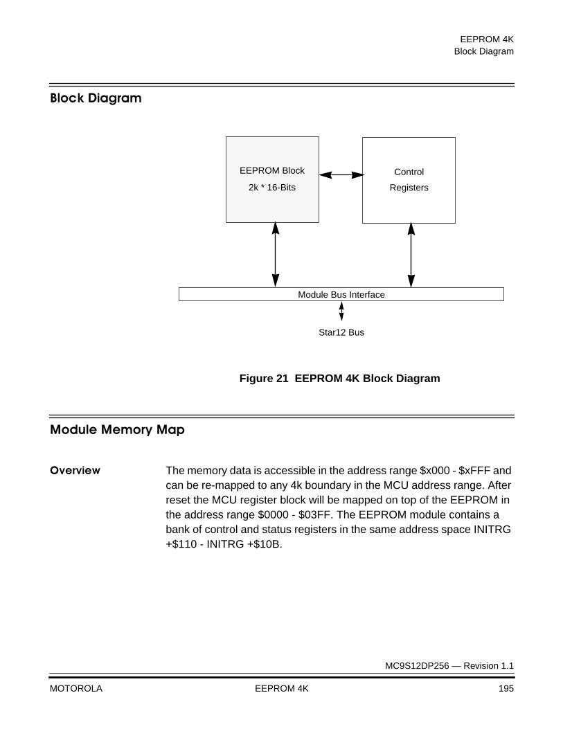
EEPROM 4KBlock Diagram
MC9S12DP256 — Revision 1.1
MOTOROLA EEPROM 4K 195
Block Diagram
Figure 21 EEPROM 4K Block Diagram
Module Memory Map
Overview The memory data is accessible in the address range $x000 - $xFFF and can be re-mapped to any 4k boundary in the MCU address range. After reset the MCU register block will be mapped on top of the EEPROM in the address range $0000 - $03FF. The EEPROM module contains a bank of control and status registers in the same address space INITRG +$110 - INITRG +$10B.
EEPROM Block
2k * 16-Bits
Module Bus Interface
Star12 Bus
Control
Registers
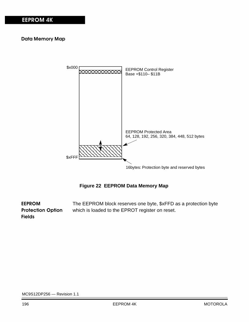
EEPROM 4K
MC9S12DP256 — Revision 1.1
196 EEPROM 4K MOTOROLA
Data Memory Map
Figure 22 EEPROM Data Memory Map
EEPROM Protection Option Fields
The EEPROM block reserves one byte, $xFFD as a protection byte which is loaded to the EPROT register on reset.
$x000 EEPROM Control RegisterBase +$110– $11B
EEPROM Protected Area64, 128, 192, 256, 320, 384, 448, 512 bytes
$xFFF
16bytes: Protection byte and reserved bytes
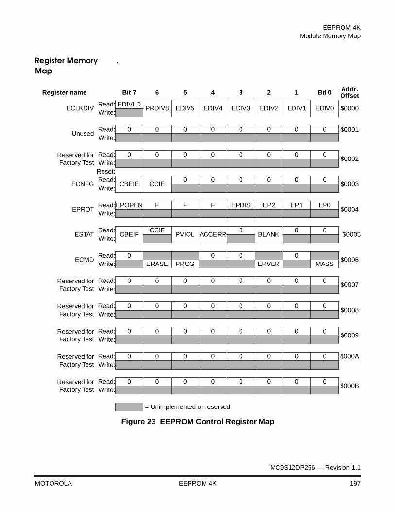
EEPROM 4KModule Memory Map
MC9S12DP256 — Revision 1.1
MOTOROLA EEPROM 4K 197
Register Memory Map
.
Register name Bit 7 6 5 4 3 2 1 Bit 0 Addr.Offset
ECLKDIVRead: EDIVLD
PRDIV8 EDIV5 EDIV4 EDIV3 EDIV2 EDIV1 EDIV0 $0000Write:
UnusedRead: 0 0 0 0 0 0 0 0 $0001Write:
Reserved forFactory Test
Read: 0 0 0 0 0 0 0 0$0002
Write:Reset:
ECNFGRead:
CBEIE CCIE0 0 0 0 0 0
$0003Write:
EPROTRead:EPOPEN F F F EPDIS EP2 EP1 EP0
$0004Write:
ESTATRead:
CBEIFCCIF
PVIOL ACCERR0
BLANK0 0
$0005Write:
ECMDRead: 0 0 0 0
$0006Write: ERASE PROG ERVER MASS
Reserved forFactory Test
Read: 0 0 0 0 0 0 0 0$0007
Write:
Reserved forFactory Test
Read: 0 0 0 0 0 0 0 0$0008
Write:
Reserved forFactory Test
Read: 0 0 0 0 0 0 0 0$0009
Write:
Reserved forFactory Test
Read: 0 0 0 0 0 0 0 0 $000AWrite:
Reserved forFactory Test
Read: 0 0 0 0 0 0 0 0$000B
Write:
= Unimplemented or reserved
Figure 23 EEPROM Control Register Map
EEPROM 4K
MC9S12DP256 — Revision 1.1
198 EEPROM 4K MOTOROLA
NOTE: Register Address = Base Address + Address Offset, where the Base Address is defined at the MCU level and the Address Offset is defined at the module level.
Functional Description
All internal program and erase timings are handled by a state machine. The timebase is derived from the oscillator clock OSCCLK via a programmable down counter. The command register as well as the associated address and data registers operate as a buffer and a register (2-stage FIFO), so that a new command along with the necessary data and address can be stored to the buffers while the previous command is still in progress. Buffers empty situation as well as command completion are signalled by flags in the status register. Interrupts will be generated if enabled.
Program and Erase Procedures
Prior to issuing any program or erase commands it is first necessary to program the ECLKDIV register to divide the oscillator clock to within the 150KHz to 200KHz range. Program and erase commands will not function if this register has not been initialized. See ECLKDIV register description for further details.
A Command State Machine is used to supervise the command sequence.
The CBEIF flag should be tested to ensure that the address, data and command buffers are empty. If so, the command sequence can be started. The 3-step command sequence must be strictly adhered to and no intermediate writes to EEPROM registers are permitted between the 3 steps. The command sequence is as follows:
EEPROM 4KFunctional Description
MC9S12DP256 — Revision 1.1
MOTOROLA EEPROM 4K 199
1. Write an aligned data word (16-bits) to be programmed to the EEPROM address space between $x000 and $xFFF. The address and data will be stored in internal buffers. For program, all address bits are valid. For erase, the value of the data bytes is don’t care. For mass erase the address can be anywhere in the available address space of the 4k byte block to be erased. For sector erase the address bits 1:0 are don’t cared.
2. Write the program or erase command to the command buffer.
3. Reset CBEIF flag by writing a “1”. This will launch the command. The ACCERR and PVIOL flags should be tested to ensure the command sequence was valid. Five cycles after the CBEIF flag is cleared the CCIF flag will be cleared by hardware indicating that the command was successfully launched. The CBEIF flag will be set again indicating the address, data and command buffers are ready for a new command sequence to begin.
The completion of the command is indicated by the CCIF flag setting (Command Complete Interrupt Flag)
The Command State Machine will flag errors in program or erase sequences by means of the ACCERR (access error) and PVIOL (protection violation) flags in the FSTAT register. An erroneous command sequence will immediately abort and set the appropriate flag. The user has then to clear the ACCERR or PVIOL flags before being able to commence another command sequence.
The ACCERR flag will be set during the command sequence if any of the following illegal operations are performed. Such operations will cause the command sequence to immediately abort:
1. Writing to the EEPROM address space before initializing ECLKDIV.
2. Writing a misaligned word or a byte to the EEPROM address space.
3. Writing to the EEPROM address space while CBEIF is not set.
4. Writing a second aligned word to the EEPROM address space before executing a program or erase command on the previously written word.
5. Writing to any EEPROM register other than ECMD after writing an aligned word to the EEPROM address space.
EEPROM 4K
MC9S12DP256 — Revision 1.1
200 EEPROM 4K MOTOROLA
6. Writing a second command to the ECMD register before executing the previously written command.
7. Writing a MASS erase command to ECMD while any protection is enabled. See EPROT register description.
8. Writing a SECTOR erase command to ECMD while protection is enabled for that sector. See EPROT register description.
9. Writing to any EEPROM register other than ESTAT (to clear CBEIF) after writing to the command register.
10. Reading from the EEPROM array while a command sequence is being entered or a program or erase command is being executed (i.e. CCIF not set). Such a read access returns non valid data.
NOTE: By writing a 0 to the CBEIF flag the command sequence can be aborted after the aligned word write to the flash address space or after writing a command to the ECMD register and before the command is launched.
The PVIOL flag will be set after the aligned write to the EEPROM address space if an attempt to program or erase a protected area of the EEPROM array is made. Such an operation will cause the command sequence to immediately abort. The user must clear the PVIOL flag before being able to commence another command sequence.
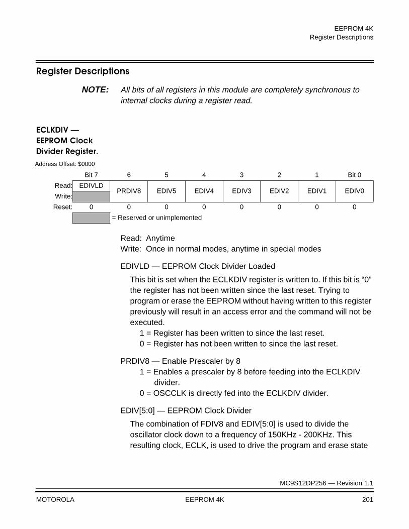
EEPROM 4KRegister Descriptions
MC9S12DP256 — Revision 1.1
MOTOROLA EEPROM 4K 201
Register Descriptions
NOTE: All bits of all registers in this module are completely synchronous to internal clocks during a register read.
ECLKDIV Ñ EEPROM Clock Divider Register.
Read: AnytimeWrite: Once in normal modes, anytime in special modes
EDIVLD — EEPROM Clock Divider Loaded
This bit is set when the ECLKDIV register is written to. If this bit is “0” the register has not been written since the last reset. Trying to program or erase the EEPROM without having written to this register previously will result in an access error and the command will not be executed.
1 = Register has been written to since the last reset.0 = Register has not been written to since the last reset.
PRDIV8 — Enable Prescaler by 81 = Enables a prescaler by 8 before feeding into the ECLKDIV
divider.0 = OSCCLK is directly fed into the ECLKDIV divider.
EDIV[5:0] — EEPROM Clock Divider
The combination of FDIV8 and EDIV[5:0] is used to divide the oscillator clock down to a frequency of 150KHz - 200KHz. This resulting clock, ECLK, is used to drive the program and erase state
Address Offset: $0000
Bit 7 6 5 4 3 2 1 Bit 0
Read: EDIVLDPRDIV8 EDIV5 EDIV4 EDIV3 EDIV2 EDIV1 EDIV0
Write:
Reset: 0 0 0 0 0 0 0 0
= Reserved or unimplemented
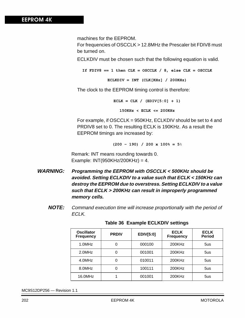
EEPROM 4K
MC9S12DP256 — Revision 1.1
202 EEPROM 4K MOTOROLA
machines for the EEPROM.For frequencies of OSCCLK > 12.8MHz the Prescaler bit FDIV8 must be turned on.
ECLKDIV must be chosen such that the following equation is valid.
If FDIV8 == 1 then CLK = OSCCLK / 8, else CLK = OSCCLK
ECLKDIV = INT (CLK[KHz] / 200KHz)
The clock to the EEPROM timing control is therefore:
ECLK = CLK / (EDIV[5:0] + 1)
150KHz < ECLK <= 200KHz
For example, if OSCCLK = 950KHz, ECLKDIV should be set to 4 and PRDIV8 set to 0. The resulting ECLK is 190KHz. As a result the EEPROM timings are increased by:
(200 - 190) / 200 x 100% = 5%
Remark: INT means rounding towards 0. Example: INT(950KHz/200KHz) = 4.
WARNING: Programming the EEPROM with OSCCLK < 500KHz should be avoided. Setting ECLKDIV to a value such that ECLK < 150KHz can destroy the EEPROM due to overstress. Setting ECLKDIV to a value such that ECLK > 200KHz can result in improperly programmed memory cells.
NOTE: Command execution time will increase proportionally with the period of ECLK.
Table 36 Example ECLKDIV settings
Oscillator Frequency PRDIV EDIV[5:0] ECLK
FrequencyECLKPeriod
1.0MHz 0 000100 200KHz 5us
2.0MHz 0 001001 200KHz 5us
4.0MHz 0 010011 200KHz 5us
8.0MHz 0 100111 200KHz 5us
16.0MHz 1 001001 200KHz 5us

EEPROM 4KRegister Descriptions
MC9S12DP256 — Revision 1.1
MOTOROLA EEPROM 4K 203
ECNFG Ñ EEPROM Configuration Register
Read: AnytimeWrite: Anytime
This register enables the interrupts
CBEIE — Command Buffers Empty Interrupt Enable
This bit enables the interrupts in case of an empty address, data and command buffers.
1 = An interrupt will be requested whenever the CBEIF flag is set0 = Command Buffers Empty Interrupts disabled
CCIE — Command Complete Interrupt Enable
This bit enables the interrupts in case of all commands being completed.
1 = An interrupt will be requested whenever the CCIF flag is set0 = Command Complete Interrupts disabled
Address Offset: $0003
Bit 7 6 5 4 3 2 1 Bit 0
Read:CBEIE CCIE
0 0 0 0 0 0
Write:
Reset: 0 0 0 0 0 0 0 0
= Reserved or unimplemented
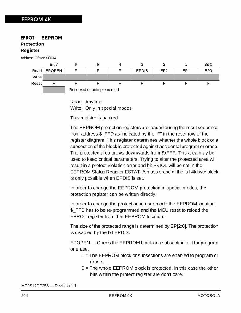
EEPROM 4K
MC9S12DP256 — Revision 1.1
204 EEPROM 4K MOTOROLA
EPROT Ñ EEPROM Protection Register
Read: AnytimeWrite: Only in special modes
This register is banked.
The EEPROM protection registers are loaded during the reset sequence from address $_FFD as indicated by the “F” in the reset row of the register diagram. This register determines whether the whole block or a subsection of the block is protected against accidental program or erase. The protected area grows downwards from $xFFF. This area may be used to keep critical parameters. Trying to alter the protected area will result in a protect violation error and bit PVIOL will be set in the EEPROM Status Register ESTAT. A mass erase of the full 4k byte block is only possible when EPDIS is set.
In order to change the EEPROM protection in special modes, the protection register can be written directly.
In order to change the protection in user mode the EEPROM location $_FFD has to be re-programmed and the MCU reset to reload the EPROT register from that EEPROM location.
The size of the protected range is determined by EP[2:0]. The protection is disabled by the bit EPDIS.
EPOPEN — Opens the EEPROM block or a subsection of it for program or erase.
1 = The EEPROM block or subsections are enabled to program or erase.
0 = The whole EEPROM block is protected. In this case the other bits within the protect register are don’t care.
Address Offset: $0004
Bit 7 6 5 4 3 2 1 Bit 0
Read: EPOPEN F F F EPDIS EP2 EP1 EP0
Write:
Reset: F F F F F F F F
= Reserved or unimplemented

EEPROM 4KRegister Descriptions
MC9S12DP256 — Revision 1.1
MOTOROLA EEPROM 4K 205
EPDIS — EEPROM Protection disableThis bit determines whether there is a protected area at the higher end of the EEPROM block address map.
1 = Protection disabled0 = Protection enabled
EP[2:0] — EEPROM Protection address sizeThese 3 bits determine the size of the protected area.
The EEPROM holds a field of 16-bytes consisting of 1 protection byte and 15 reserved bytes. The layout of this field is:
Table 37 Address Range Protection
EP[2:0] Protected Address Range
Protected Size
000 $_FC0 - $_FFF 64 bytes
001 $_F80 - $_FFF 128 bytes
010 $_F40 - $_FFF 192 bytes
011 $_F00 - $_FFF 256 bytes
100 $_EC0 - $_FFF 320 bytes
101 $_E80 - $_FFF 384 bytes
110 $_E40 - $_FFF 448 bytes
111 $_E00 - $_FFF 512 bytes
Table 38 Flash 0 Protection/Security Field
Address Size Description
$_FF0 - $_FFC 13 Reserved
$_FFD 1 Protection byte for EEPROM
$_FFE - $_FFF 2 Reserved
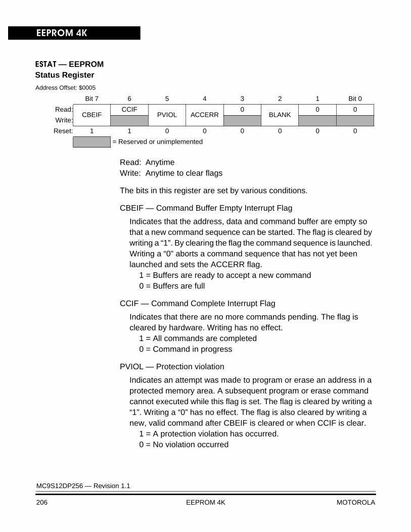
EEPROM 4K
MC9S12DP256 — Revision 1.1
206 EEPROM 4K MOTOROLA
ESTAT Ñ EEPROM Status Register
Read: AnytimeWrite: Anytime to clear flags
The bits in this register are set by various conditions.
CBEIF — Command Buffer Empty Interrupt Flag
Indicates that the address, data and command buffer are empty so that a new command sequence can be started. The flag is cleared by writing a “1”. By clearing the flag the command sequence is launched. Writing a “0” aborts a command sequence that has not yet been launched and sets the ACCERR flag.
1 = Buffers are ready to accept a new command0 = Buffers are full
CCIF — Command Complete Interrupt Flag
Indicates that there are no more commands pending. The flag is cleared by hardware. Writing has no effect.
1 = All commands are completed0 = Command in progress
PVIOL — Protection violation
Indicates an attempt was made to program or erase an address in a protected memory area. A subsequent program or erase command cannot executed while this flag is set. The flag is cleared by writing a “1”. Writing a “0” has no effect. The flag is also cleared by writing a new, valid command after CBEIF is cleared or when CCIF is clear.
1 = A protection violation has occurred.0 = No violation occurred
Address Offset: $0005
Bit 7 6 5 4 3 2 1 Bit 0
Read:CBEIF
CCIFPVIOL ACCERR
0BLANK
0 0
Write:
Reset: 1 1 0 0 0 0 0 0
= Reserved or unimplemented
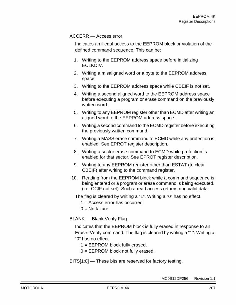
EEPROM 4KRegister Descriptions
MC9S12DP256 — Revision 1.1
MOTOROLA EEPROM 4K 207
ACCERR — Access error
Indicates an illegal access to the EEPROM block or violation of the defined command sequence. This can be:
1. Writing to the EEPROM address space before initializing ECLKDIV.
2. Writing a misaligned word or a byte to the EEPROM address space.
3. Writing to the EEPROM address space while CBEIF is not set.
4. Writing a second aligned word to the EEPROM address space before executing a program or erase command on the previously written word.
5. Writing to any EEPROM register other than ECMD after writing an aligned word to the EEPROM address space.
6. Writing a second command to the ECMD register before executing the previously written command.
7. Writing a MASS erase command to ECMD while any protection is enabled. See EPROT register description.
8. Writing a sector erase command to ECMD while protection is enabled for that sector. See EPROT register description.
9. Writing to any EEPROM register other than ESTAT (to clear CBEIF) after writing to the command register.
10. Reading from the EEPROM block while a command sequence is being entered or a program or erase command is being executed. (i.e. CCIF not set). Such a read access returns non valid data
The flag is cleared by writing a “1”. Writing a “0” has no effect.1 = Access error has occurred.0 = No failure.
BLANK — Blank Verify Flag
Indicates that the EEPROM block is fully erased in response to an Erase- Verify command. The flag is cleared by writing a “1”. Writing a “0” has no effect.
1 = EEPROM block fully erased.0 = EEPROM block not fully erased.
BITS[1:0] — These bits are reserved for factory testing.
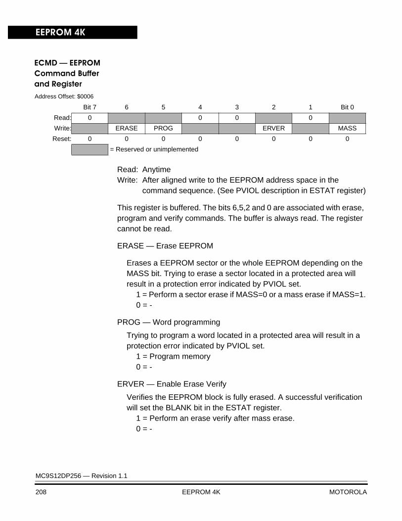
EEPROM 4K
MC9S12DP256 — Revision 1.1
208 EEPROM 4K MOTOROLA
ECMD Ñ EEPROM Command Buffer and Register
Read: AnytimeWrite: After aligned write to the EEPROM address space in the
command sequence. (See PVIOL description in ESTAT register)
This register is buffered. The bits 6,5,2 and 0 are associated with erase, program and verify commands. The buffer is always read. The register cannot be read.
ERASE — Erase EEPROM
Erases a EEPROM sector or the whole EEPROM depending on the MASS bit. Trying to erase a sector located in a protected area will result in a protection error indicated by PVIOL set.
1 = Perform a sector erase if MASS=0 or a mass erase if MASS=1.0 = -
PROG — Word programming
Trying to program a word located in a protected area will result in a protection error indicated by PVIOL set.
1 = Program memory0 = -
ERVER — Enable Erase Verify
Verifies the EEPROM block is fully erased. A successful verification will set the BLANK bit in the ESTAT register.
1 = Perform an erase verify after mass erase.0 = -
Address Offset: $0006
Bit 7 6 5 4 3 2 1 Bit 0
Read: 0 0 0 0
Write: ERASE PROG ERVER MASS
Reset: 0 0 0 0 0 0 0 0
= Reserved or unimplemented

EEPROM 4KRegister Descriptions
MC9S12DP256 — Revision 1.1
MOTOROLA EEPROM 4K 209
MASS — Enables Mass Erase
Perform a mass erase of the selected 4k byte block. This bit works in conjunction with the ERASE bit. If any protection is active on the selected block, mass erase has no effect and PVIOL is set.
1 = Perform a mass erase of the whole block0 = Perform sector erase
The registers $0007 to $000B are reserved for factory testing and are not available to the user.
Table 39 Valid Commands
Command Meaning Remarks
$20 Memory Program Program 1 word (2 bytes)
$40 Sector Erase Erase 4 bytes
$41 Mass Erase Erase all 4k bytes
$05 Erase VerifyVerify all 4k bytes are
erased
other Illegal Generate an access error
EEPROM 4K
MC9S12DP256 — Revision 1.1
210 EEPROM 4K MOTOROLA
External Pin Descriptions
This module does not have external pins relevant for the user.
Reset Initialization
Out of reset the module is immediately accessible operating in read mode.
If a reset occurs while any command is in progress that command will be immediately aborted. The state of the word being programmed or the sector / block being erased is not guaranteed.
Modes of Operation
Security Modes There are no security modes for the EEPROM.
Low Power Options When the array or the registers are not being accessed clocking to the register block is shut off to save power. The only exceptions to this are the flag bits in the ESTAT register which are updated by internal state machines.
Run Mode No special current saving modes available.
Wait Mode When the MCU enters WAIT mode and any command is active (CCIF = 0) the command will be completed. If enabled, the CCIF interrupt can be used to waken the MCU out of Wait mode.
Stop Mode No low power options exist for this module in stop mode. If a command is active (CCIF = 0) when the MCU enters the STOP mode, the command will be aborted and the and the high voltage circuitry to the EEPROM array will be switched off.
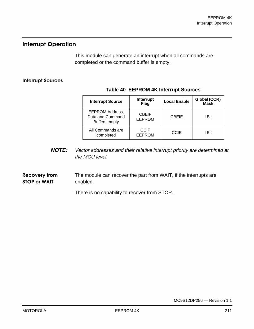
EEPROM 4KInterrupt Operation
MC9S12DP256 — Revision 1.1
MOTOROLA EEPROM 4K 211
Interrupt Operation
This module can generate an interrupt when all commands are completed or the command buffer is empty.
Interrupt Sources
NOTE: Vector addresses and their relative interrupt priority are determined at the MCU level.
Recovery from STOP or WAIT
The module can recover the part from WAIT, if the interrupts are enabled.
There is no capability to recover from STOP.
Table 40 EEPROM 4K Interrupt Sources
Interrupt Source Interrupt Flag Local Enable Global (CCR)
Mask
EEPROM Address, Data and Command
Buffers empty
CBEIFEEPROM
CBEIE I Bit
All Commands are completed
CCIFEEPROM
CCIE I Bit

EEPROM 4K
MC9S12DP256 — Revision 1.1
212 EEPROM 4K MOTOROLA
MC9S12DP256 — Revision 1.1
MOTOROLA Port Integration Module 213
Port Integration ModulePort Integration Module
Contents
Overview . . . . . . . . . . . . . . . . . . . . . . . . . . . . . . . . . . . . . . . . . . . . . . 213Block Diagram. . . . . . . . . . . . . . . . . . . . . . . . . . . . . . . . . . . . . . . . . . 215Register Map. . . . . . . . . . . . . . . . . . . . . . . . . . . . . . . . . . . . . . . . . . . 217External Pin Descriptions . . . . . . . . . . . . . . . . . . . . . . . . . . . . . . . . . 21680 Pin QFP bond-out version . . . . . . . . . . . . . . . . . . . . . . . . . . . . . . 216Register Map. . . . . . . . . . . . . . . . . . . . . . . . . . . . . . . . . . . . . . . . . . . 217Register Descriptions . . . . . . . . . . . . . . . . . . . . . . . . . . . . . . . . . . . . 222Reset Initialization . . . . . . . . . . . . . . . . . . . . . . . . . . . . . . . . . . . . . . . 251Functional Description. . . . . . . . . . . . . . . . . . . . . . . . . . . . . . . . . . . . 251Low Power Options . . . . . . . . . . . . . . . . . . . . . . . . . . . . . . . . . . . . . . 255Interrupt Operation . . . . . . . . . . . . . . . . . . . . . . . . . . . . . . . . . . . . . . 256
Overview
The Port Integration Module establishes the interface between the peripheral modules and the I/O pins for all ports except A, B, E and K. Those ports are handled by the HC12 multiplexed bus interface and described in Bus Control and Input/Output, due to their tight link with the external bus interface and special modes.
The two 8-bit ports associated with the ATD are included in the ATD module due to their sensitivity to electrical noise, requiring special care on routing and design.
This section covers port T connected to the timer module, the serial port S associated with 2 SCI and 1 SPI module, the multiplex ports M, associated with 4 CAN and 1 BDLC module, and P, connected to the PWM and 2 SPI modules, the standard I/O port H, and finally the port J

Port Integration Module
MC9S12DP256 — Revision 1.1
214 Port Integration Module MOTOROLA
associated with the fifth CAN module and the IIC interface1. Ports P, H and J can also be used as external interrupt sources.
Each I/O pin can be configured by several registers: Input/output selection, drive strength reduction, enable and select of pull resistors, interrupt enable and status flags.
The port integration module is device dependant which is reflected in its naming.
A standard port has the following minimum features:
• Input/output selection
• 5V output drive with two selectable drive strength
• 5V digital and analog input
• Input with selectable pull-up or pull-down device
Optional features:
• Open drain for wired-or connections
• Interrupt inputs with glitch filtering
1. The port control register addresses are allocated in the order of their most likely occurrence, i.e. almost all STAR12 derivatives will have a timer port, and a very limited number will have a IIC module. This allows best consistency in the address allocation.
Table 41 Port Reset State and Priority Summary
Port
Reset States
PriorityData Direction Pull Mode Red. Drive Wired-Or
ModeInter-rupt
T input hiz disabled n/a n/a ECT > GPIO
S input pull-up disabled disabled n/a SCI, SPI > GPIO
M input hiz disabled disabled n/a CAN > BDLC > GPIO
P input hiz disabled n/a disabled PWM > SPI > GPIO
H input hiz disabled n/a disabled GPIO
J input pull-up disabled n/a disabled CAN > IIC > GPIO
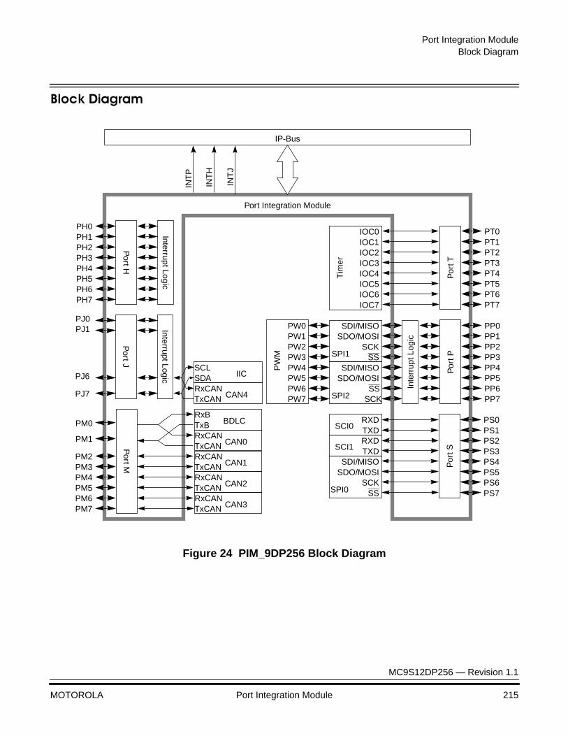
Port Integration ModuleBlock Diagram
MC9S12DP256 — Revision 1.1
MOTOROLA Port Integration Module 215
Block Diagram
Figure 24 PIM_9DP256 Block Diagram
Por
t T
PT0PT1PT2PT3PT4PT5PT6PT7
Tim
er
IOC0IOC1IOC2IOC3IOC4IOC5IOC6IOC7
Por
t P
PP0PP1PP2PP3PP4PP5PP6PP7
PW
M
PW0PW1PW2PW3PW4PW5PW6PW7
Por
t S
PS0PS1PS2PS3PS4PS5PS6PS7
RXDTXDRXDTXD
SDI/MISOSDO/MOSI
SCKSS
SCI0
SCI1
SPI0
Port H
PH0PH1PH2PH3PH4PH5PH6PH7
Port J
PJ0PJ1
PJ6
PJ7
Port M
PM0
PM1
PM2PM3PM4PM5PM6PM7 CAN3TxCAN
RxCAN
CAN1TxCANRxCAN
CAN2TxCANRxCAN
CAN0TxCANRxCAN
BDLCTxBRxB
IICSDASCL
Port Integration Module
IP-Bus
INT
J
INT
H
Interrupt LogicCAN4TxCAN
RxCAN
Interrupt Logic
SDI/MISOSDO/MOSI
SCKSSSPI1
Inte
rrup
t Log
ic
SDI/MISOSDO/MOSI
SCKSS
SPI2
INT
P
Port Integration Module
MC9S12DP256 — Revision 1.1
216 Port Integration Module MOTOROLA
External Pin Descriptions
All ports start up as general purpose inputs on reset.
80 Pin QFP bond-out version
In case the port pins are not bonded out in the chosen package the user should initialize the registers to be inputs with enabled pull resistance to avoid excess current consumption. This applies to the following pins:
• All port K and H.
• Port PP6, PJ1–0, PM7–4.
• PAD15–8. The A/D converter associated with those pins (ATD1) should be disabled.
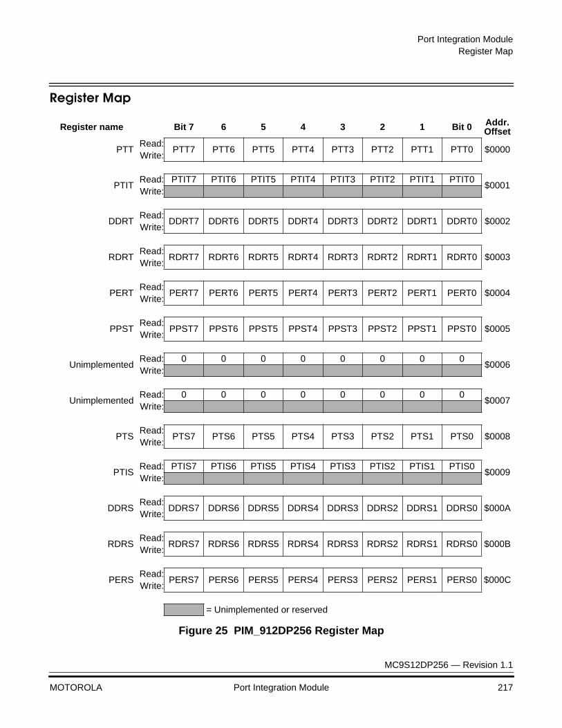
Port Integration ModuleRegister Map
MC9S12DP256 — Revision 1.1
MOTOROLA Port Integration Module 217
Register Map
Register name Bit 7 6 5 4 3 2 1 Bit 0 Addr.Offset
PTTRead:
PTT7 PTT6 PTT5 PTT4 PTT3 PTT2 PTT1 PTT0 $0000Write:
PTITRead: PTIT7 PTIT6 PTIT5 PTIT4 PTIT3 PTIT2 PTIT1 PTIT0
$0001Write:
DDRTRead:
DDRT7 DDRT6 DDRT5 DDRT4 DDRT3 DDRT2 DDRT1 DDRT0 $0002Write:
RDRTRead:
RDRT7 RDRT6 RDRT5 RDRT4 RDRT3 RDRT2 RDRT1 RDRT0 $0003Write:
PERTRead:
PERT7 PERT6 PERT5 PERT4 PERT3 PERT2 PERT1 PERT0 $0004Write:
PPSTRead:
PPST7 PPST6 PPST5 PPST4 PPST3 PPST2 PPST1 PPST0 $0005Write:
UnimplementedRead: 0 0 0 0 0 0 0 0
$0006Write:
UnimplementedRead: 0 0 0 0 0 0 0 0
$0007Write:
PTSRead:
PTS7 PTS6 PTS5 PTS4 PTS3 PTS2 PTS1 PTS0 $0008Write:
PTISRead: PTIS7 PTIS6 PTIS5 PTIS4 PTIS3 PTIS2 PTIS1 PTIS0
$0009Write:
DDRSRead:
DDRS7 DDRS6 DDRS5 DDRS4 DDRS3 DDRS2 DDRS1 DDRS0 $000AWrite:
RDRSRead:
RDRS7 RDRS6 RDRS5 RDRS4 RDRS3 RDRS2 RDRS1 RDRS0 $000BWrite:
PERSRead:
PERS7 PERS6 PERS5 PERS4 PERS3 PERS2 PERS1 PERS0 $000CWrite:
= Unimplemented or reserved
Figure 25 PIM_912DP256 Register Map
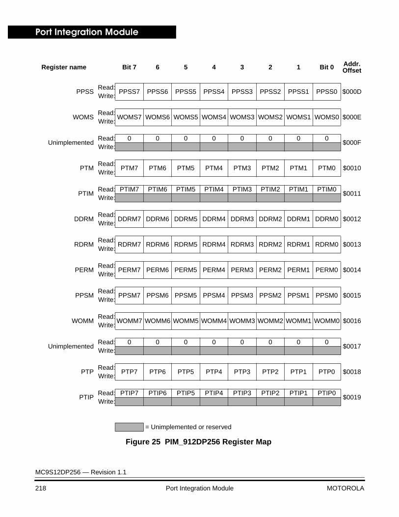
Port Integration Module
MC9S12DP256 — Revision 1.1
218 Port Integration Module MOTOROLA
PPSSRead:
PPSS7 PPSS6 PPSS5 PPSS4 PPSS3 PPSS2 PPSS1 PPSS0 $000DWrite:
WOMSRead:
WOMS7 WOMS6 WOMS5 WOMS4 WOMS3 WOMS2 WOMS1 WOMS0 $000EWrite:
UnimplementedRead: 0 0 0 0 0 0 0 0
$000FWrite:
PTMRead:
PTM7 PTM6 PTM5 PTM4 PTM3 PTM2 PTM1 PTM0 $0010Write:
PTIMRead: PTIM7 PTIM6 PTIM5 PTIM4 PTIM3 PTIM2 PTIM1 PTIM0
$0011Write:
DDRMRead:
DDRM7 DDRM6 DDRM5 DDRM4 DDRM3 DDRM2 DDRM1 DDRM0 $0012Write:
RDRMRead:
RDRM7 RDRM6 RDRM5 RDRM4 RDRM3 RDRM2 RDRM1 RDRM0 $0013Write:
PERMRead:
PERM7 PERM6 PERM5 PERM4 PERM3 PERM2 PERM1 PERM0 $0014Write:
PPSMRead:
PPSM7 PPSM6 PPSM5 PPSM4 PPSM3 PPSM2 PPSM1 PPSM0 $0015Write:
WOMMRead:
WOMM7 WOMM6 WOMM5 WOMM4 WOMM3 WOMM2 WOMM1 WOMM0 $0016Write:
UnimplementedRead: 0 0 0 0 0 0 0 0
$0017Write:
PTPRead:
PTP7 PTP6 PTP5 PTP4 PTP3 PTP2 PTP1 PTP0 $0018Write:
PTIPRead: PTIP7 PTIP6 PTIP5 PTIP4 PTIP3 PTIP2 PTIP1 PTIP0
$0019Write:
Register name Bit 7 6 5 4 3 2 1 Bit 0 Addr.Offset
= Unimplemented or reserved
Figure 25 PIM_912DP256 Register Map

Port Integration ModuleRegister Map
MC9S12DP256 — Revision 1.1
MOTOROLA Port Integration Module 219
DDRPRead:
DDRP7 DDRP6 DDRP5 DDRP4 DDRP3 DDRP2 DDRP1 DDRP0 $001AWrite:
RDRPRead:
RDRP7 RDRP6 RDRP5 RDRP4 RDRP3 RDRP2 RDRP1 RDRP0 $001BWrite:
PERPRead:
PERP7 PERP6 PERP5 PERP4 PERP3 PERP2 PERP1 PERP0 $001CWrite:
PPSPRead:
PPSP7 PPSP6 PPSP5 PPSP4 PPSP3 PPSP2 PPSP1 PPSP0 $001DWrite:
PIEPRead:
PIEP7 PIEP6 PIEP5 PIEP4 PIEP3 PIEP2 PIEP1 PIEP0 $001EWrite:
PIFPRead:
PIFP7 PIFP6 PIFP5 PIFP4 PIFP3 PIFP2 PIFP1 PIFP0 $001FWrite:
PTHRead:
PTH7 PTH6 PTH5 PTH4 PTH3 PTH2 PTH1 PTH0 $0020Write:
PTIHRead: PTIH7 PTIH6 PTIH5 PTIH4 PTIH3 PTIH2 PTIH1 PTIH0
$0021Write:
DDRHRead:
DDRH7 DDRH6 DDRH5 DDRH4 DDRH3 DDRH2 DDRH1 DDRH0 $0022Write:
RDRHRead:
RDRH7 RDRH6 RDRH5 RDRH4 RDRH3 RDRH2 RDRH1 RDRH0 $0023Write:
PERHRead:
PERH7 PERH6 PERH5 PERH4 PERH3 PERH2 PERH1 PERH0 $0024Write:
PPSHRead:
PPSH7 PPSH6 PPSH5 PPSH4 PPSH3 PPSH2 PPSH1 PPSH0 $0025Write:
PIEHRead:
PIEH7 PIEH6 PIEH5 PIEH4 PIEH3 PIEH2 PIEH1 PIEH0 $0026Write:
PIFHRead:
PIFH7 PIFH6 PIFH5 PIFH4 PIFH3 PIFH2 PIFH1 PIFH0 $0027Write:
Register name Bit 7 6 5 4 3 2 1 Bit 0 Addr.Offset
= Unimplemented or reserved
Figure 25 PIM_912DP256 Register Map
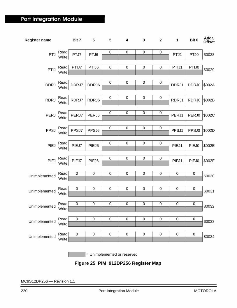
Port Integration Module
MC9S12DP256 — Revision 1.1
220 Port Integration Module MOTOROLA
PTJRead:
PTJ7 PTJ60 0 0 0
PTJ1 PTJ0 $0028Write:
PTIJRead: PTIJ7 PTIJ6 0 0 0 0 PTIJ1 PTIJ0
$0029Write:
DDRJRead:
DDRJ7 DDRJ60 0 0 0
DDRJ1 DDRJ0 $002AWrite:
RDRJRead:
RDRJ7 RDRJ60 0 0 0
RDRJ1 RDRJ0 $002BWrite:
PERJRead:
PERJ7 PERJ60 0 0 0
PERJ1 PERJ0 $002CWrite:
PPSJRead:
PPSJ7 PPSJ60 0 0 0
PPSJ1 PPSJ0 $002DWrite:
PIEJRead:
PIEJ7 PIEJ60 0 0 0
PIEJ1 PIEJ0 $002EWrite:
PIFJRead:
PIFJ7 PIFJ60 0 0 0
PIFJ1 PIFJ0 $002FWrite:
UnimplementedRead: 0 0 0 0 0 0 0 0
$0030Write:
UnimplementedRead: 0 0 0 0 0 0 0 0
$0031Write:
UnimplementedRead: 0 0 0 0 0 0 0 0
$0032Write:
UnimplementedRead: 0 0 0 0 0 0 0 0
$0033Write:
UnimplementedRead: 0 0 0 0 0 0 0 0
$0034Write:
Register name Bit 7 6 5 4 3 2 1 Bit 0 Addr.Offset
= Unimplemented or reserved
Figure 25 PIM_912DP256 Register Map
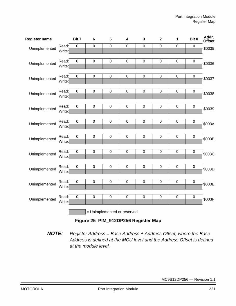
Port Integration ModuleRegister Map
MC9S12DP256 — Revision 1.1
MOTOROLA Port Integration Module 221
NOTE: Register Address = Base Address + Address Offset, where the Base Address is defined at the MCU level and the Address Offset is defined at the module level.
UnimplementedRead: 0 0 0 0 0 0 0 0
$0035Write:
UnimplementedRead: 0 0 0 0 0 0 0 0
$0036Write:
UnimplementedRead: 0 0 0 0 0 0 0 0
$0037Write:
UnimplementedRead: 0 0 0 0 0 0 0 0
$0038Write:
UnimplementedRead: 0 0 0 0 0 0 0 0
$0039Write:
UnimplementedRead: 0 0 0 0 0 0 0 0
$003AWrite:
UnimplementedRead: 0 0 0 0 0 0 0 0
$003BWrite:
UnimplementedRead: 0 0 0 0 0 0 0 0
$003CWrite:
UnimplementedRead: 0 0 0 0 0 0 0 0
$003DWrite:
UnimplementedRead: 0 0 0 0 0 0 0 0
$003EWrite:
UnimplementedRead: 0 0 0 0 0 0 0 0
$003FWrite:
Register name Bit 7 6 5 4 3 2 1 Bit 0 Addr.Offset
= Unimplemented or reserved
Figure 25 PIM_912DP256 Register Map
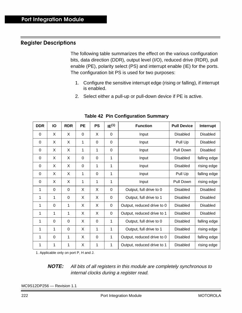
Port Integration Module
MC9S12DP256 — Revision 1.1
222 Port Integration Module MOTOROLA
Register Descriptions
The following table summarizes the effect on the various configuration bits, data direction (DDR), output level (I/O), reduced drive (RDR), pull enable (PE), polarity select (PS) and interrupt enable (IE) for the ports. The configuration bit PS is used for two purposes:
1. Configure the sensitive interrupt edge (rising or falling), if interrupt is enabled.
2. Select either a pull-up or pull-down device if PE is active.
NOTE: All bits of all registers in this module are completely synchronous to internal clocks during a register read.
Table 42 Pin Configuration Summary
DDR IO RDR PE PS IE(1) Function Pull Device Interrupt
0 X X 0 X 0 Input Disabled Disabled
0 X X 1 0 0 Input Pull Up Disabled
0 X X 1 1 0 Input Pull Down Disabled
0 X X 0 0 1 Input Disabled falling edge
0 X X 0 1 1 Input Disabled rising edge
0 X X 1 0 1 Input Pull Up falling edge
0 X X 1 1 1 Input Pull Down rising edge
1 0 0 X X 0 Output, full drive to 0 Disabled Disabled
1 1 0 X X 0 Output, full drive to 1 Disabled Disabled
1 0 1 X X 0 Output, reduced drive to 0 Disabled Disabled
1 1 1 X X 0 Output, reduced drive to 1 Disabled Disabled
1 0 0 X 0 1 Output, full drive to 0 Disabled falling edge
1 1 0 X 1 1 Output, full drive to 1 Disabled rising edge
1 0 1 X 0 1 Output, reduced drive to 0 Disabled falling edge
1 1 1 X 1 1 Output, reduced drive to 1 Disabled rising edge
1. Applicable only on port P, H and J.
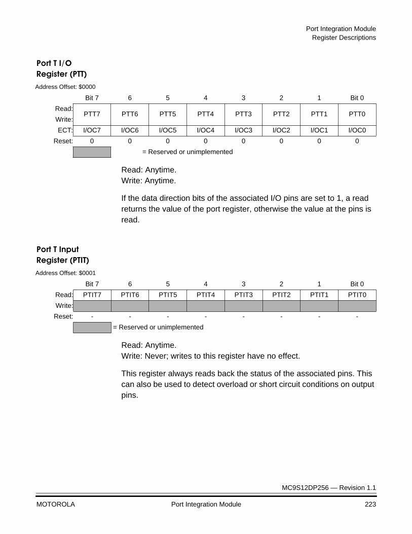
Port Integration ModuleRegister Descriptions
MC9S12DP256 — Revision 1.1
MOTOROLA Port Integration Module 223
Port T I/ORegister (PTT)
Read: Anytime.Write: Anytime.
If the data direction bits of the associated I/O pins are set to 1, a read returns the value of the port register, otherwise the value at the pins is read.
Port T Input Register (PTIT)
Read: Anytime.Write: Never; writes to this register have no effect.
This register always reads back the status of the associated pins. This can also be used to detect overload or short circuit conditions on output pins.
Address Offset: $0000
Bit 7 6 5 4 3 2 1 Bit 0
Read:PTT7 PTT6 PTT5 PTT4 PTT3 PTT2 PTT1 PTT0
Write:
ECT: I/OC7 I/OC6 I/OC5 I/OC4 I/OC3 I/OC2 I/OC1 I/OC0
Reset: 0 0 0 0 0 0 0 0
= Reserved or unimplemented
Address Offset: $0001
Bit 7 6 5 4 3 2 1 Bit 0
Read: PTIT7 PTIT6 PTIT5 PTIT4 PTIT3 PTIT2 PTIT1 PTIT0
Write:
Reset: - - - - - - - -
= Reserved or unimplemented
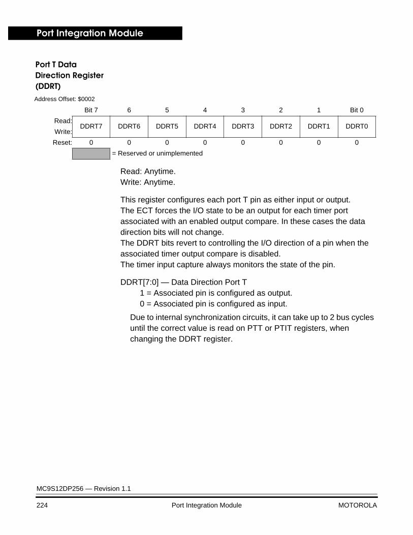
Port Integration Module
MC9S12DP256 — Revision 1.1
224 Port Integration Module MOTOROLA
Port T Data Direction Register (DDRT)
Read: Anytime.Write: Anytime.
This register configures each port T pin as either input or output.The ECT forces the I/O state to be an output for each timer port associated with an enabled output compare. In these cases the data direction bits will not change. The DDRT bits revert to controlling the I/O direction of a pin when the associated timer output compare is disabled. The timer input capture always monitors the state of the pin.
DDRT[7:0] — Data Direction Port T1 = Associated pin is configured as output.0 = Associated pin is configured as input.
Due to internal synchronization circuits, it can take up to 2 bus cycles until the correct value is read on PTT or PTIT registers, when changing the DDRT register.
Address Offset: $0002
Bit 7 6 5 4 3 2 1 Bit 0
Read:DDRT7 DDRT6 DDRT5 DDRT4 DDRT3 DDRT2 DDRT1 DDRT0
Write:
Reset: 0 0 0 0 0 0 0 0
= Reserved or unimplemented
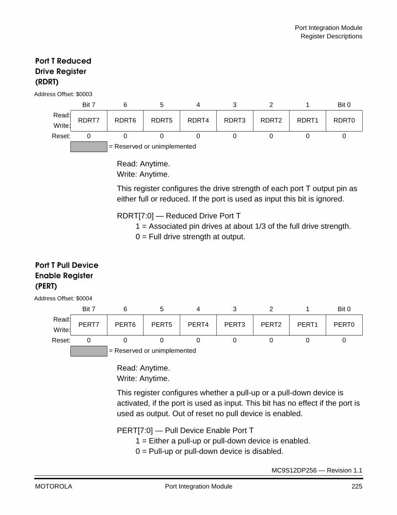
Port Integration ModuleRegister Descriptions
MC9S12DP256 — Revision 1.1
MOTOROLA Port Integration Module 225
Port T Reduced Drive Register (RDRT)
Read: Anytime.Write: Anytime.
This register configures the drive strength of each port T output pin as either full or reduced. If the port is used as input this bit is ignored.
RDRT[7:0] — Reduced Drive Port T1 = Associated pin drives at about 1/3 of the full drive strength.0 = Full drive strength at output.
Port T Pull Device Enable Register (PERT)
Read: Anytime.Write: Anytime.
This register configures whether a pull-up or a pull-down device is activated, if the port is used as input. This bit has no effect if the port is used as output. Out of reset no pull device is enabled.
PERT[7:0] — Pull Device Enable Port T1 = Either a pull-up or pull-down device is enabled.0 = Pull-up or pull-down device is disabled.
Address Offset: $0003
Bit 7 6 5 4 3 2 1 Bit 0
Read:RDRT7 RDRT6 RDRT5 RDRT4 RDRT3 RDRT2 RDRT1 RDRT0
Write:
Reset: 0 0 0 0 0 0 0 0
= Reserved or unimplemented
Address Offset: $0004
Bit 7 6 5 4 3 2 1 Bit 0
Read:PERT7 PERT6 PERT5 PERT4 PERT3 PERT2 PERT1 PERT0
Write:
Reset: 0 0 0 0 0 0 0 0
= Reserved or unimplemented
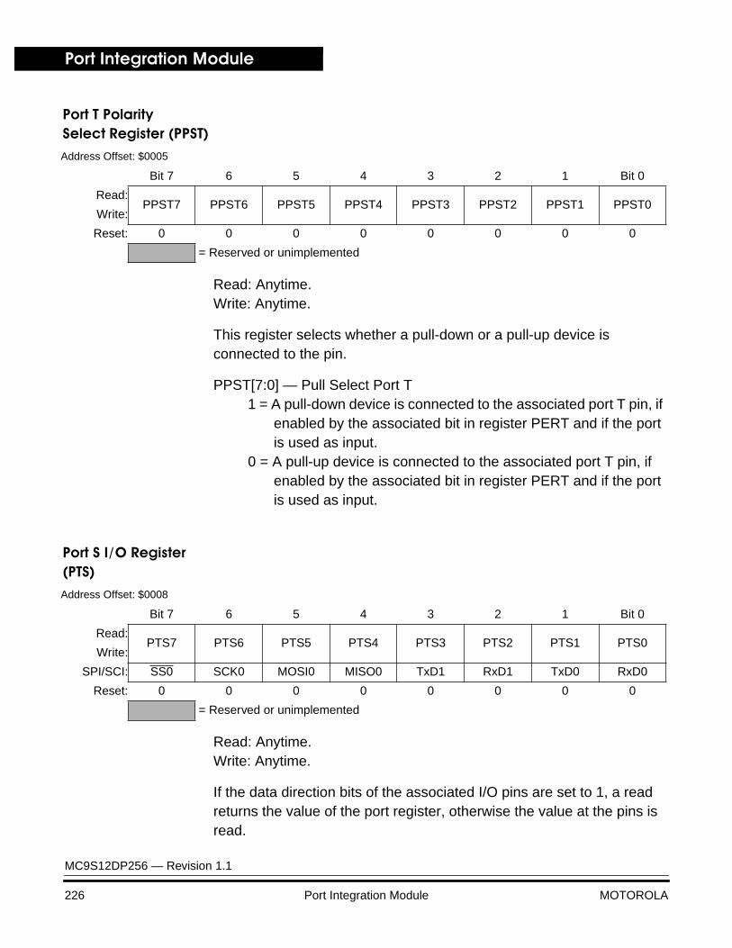
Port Integration Module
MC9S12DP256 — Revision 1.1
226 Port Integration Module MOTOROLA
Port T PolaritySelect Register (PPST)
Read: Anytime.Write: Anytime.
This register selects whether a pull-down or a pull-up device is connected to the pin.
PPST[7:0] — Pull Select Port T1 = A pull-down device is connected to the associated port T pin, if
enabled by the associated bit in register PERT and if the port is used as input.
0 = A pull-up device is connected to the associated port T pin, if enabled by the associated bit in register PERT and if the port is used as input.
Port S I/O Register (PTS)
Read: Anytime.Write: Anytime.
If the data direction bits of the associated I/O pins are set to 1, a read returns the value of the port register, otherwise the value at the pins is read.
Address Offset: $0005
Bit 7 6 5 4 3 2 1 Bit 0
Read:PPST7 PPST6 PPST5 PPST4 PPST3 PPST2 PPST1 PPST0
Write:
Reset: 0 0 0 0 0 0 0 0
= Reserved or unimplemented
Address Offset: $0008
Bit 7 6 5 4 3 2 1 Bit 0
Read:PTS7 PTS6 PTS5 PTS4 PTS3 PTS2 PTS1 PTS0
Write:
SPI/SCI: SS0 SCK0 MOSI0 MISO0 TxD1 RxD1 TxD0 RxD0
Reset: 0 0 0 0 0 0 0 0
= Reserved or unimplemented
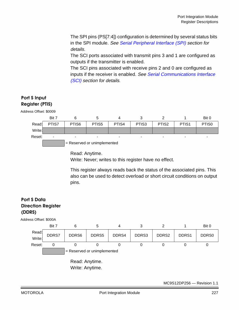
Port Integration ModuleRegister Descriptions
MC9S12DP256 — Revision 1.1
MOTOROLA Port Integration Module 227
The SPI pins (PS[7:4]) configuration is determined by several status bits in the SPI module. See Serial Peripheral Interface (SPI) section for details.The SCI ports associated with transmit pins 3 and 1 are configured as outputs if the transmitter is enabled.The SCI pins associated with receive pins 2 and 0 are configured as inputs if the receiver is enabled. See Serial Communications Interface (SCI) section for details.
Port S Input Register (PTIS)
Read: Anytime.Write: Never; writes to this register have no effect.
This register always reads back the status of the associated pins. This also can be used to detect overload or short circuit conditions on output pins.
Port S Data Direction Register (DDRS)
Read: Anytime.Write: Anytime.
Address Offset: $0009
Bit 7 6 5 4 3 2 1 Bit 0
Read: PTIS7 PTIS6 PTIS5 PTIS4 PTIS3 PTIS2 PTIS1 PTIS0
Write:
Reset: - - - - - - - -
= Reserved or unimplemented
Address Offset: $000A
Bit 7 6 5 4 3 2 1 Bit 0
Read:DDRS7 DDRS6 DDRS5 DDRS4 DDRS3 DDRS2 DDRS1 DDRS0
Write:
Reset: 0 0 0 0 0 0 0 0
= Reserved or unimplemented
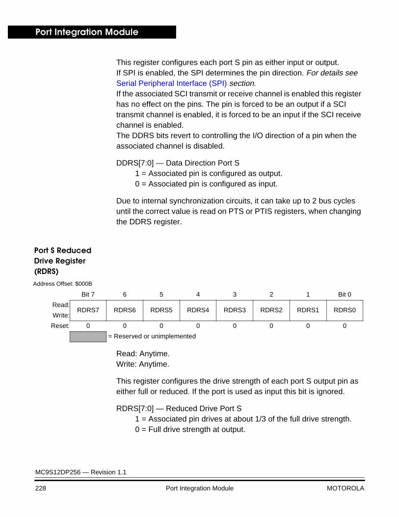
Port Integration Module
MC9S12DP256 — Revision 1.1
228 Port Integration Module MOTOROLA
This register configures each port S pin as either input or output.If SPI is enabled, the SPI determines the pin direction. For details see Serial Peripheral Interface (SPI) section. If the associated SCI transmit or receive channel is enabled this register has no effect on the pins. The pin is forced to be an output if a SCI transmit channel is enabled, it is forced to be an input if the SCI receive channel is enabled. The DDRS bits revert to controlling the I/O direction of a pin when the associated channel is disabled.
DDRS[7:0] — Data Direction Port S1 = Associated pin is configured as output.0 = Associated pin is configured as input.
Due to internal synchronization circuits, it can take up to 2 bus cycles until the correct value is read on PTS or PTIS registers, when changing the DDRS register.
Port S Reduced Drive Register (RDRS)
Read: Anytime.Write: Anytime.
This register configures the drive strength of each port S output pin as either full or reduced. If the port is used as input this bit is ignored.
RDRS[7:0] — Reduced Drive Port S1 = Associated pin drives at about 1/3 of the full drive strength.0 = Full drive strength at output.
Address Offset: $000B
Bit 7 6 5 4 3 2 1 Bit 0
Read:RDRS7 RDRS6 RDRS5 RDRS4 RDRS3 RDRS2 RDRS1 RDRS0
Write:
Reset: 0 0 0 0 0 0 0 0
= Reserved or unimplemented

Port Integration ModuleRegister Descriptions
MC9S12DP256 — Revision 1.1
MOTOROLA Port Integration Module 229
Port S Pull Device Enable Register (PERS)
Read: Anytime.Write: Anytime.
This register configures whether a pull-up or a pull-down device is activated, if the port is used as input or as output in wired-or (open drain) mode. This bit has no effect if the port is used as push-pull output. Out of reset a pull-up device is enabled.
PERS[7:0] — Pull Device Enable Port S1 = Either a pull-up or pull-down device is enabled.0 = Pull-up or pull-down device is disabled.
Port S Polarity Select Register (PPSS)
Read: Anytime.Write: Anytime.
This register selects whether a pull-down or a pull-up device is connected to the pin.
Address Offset: $000C
Bit 7 6 5 4 3 2 1 Bit 0
Read:PERS7 PERS6 PERS5 PERS4 PERS3 PERS2 PERS1 PERS0
Write:
Reset: 1 1 1 1 1 1 1 1
= Reserved or unimplemented
Address Offset: $000D
Bit 7 6 5 4 3 2 1 Bit 0
Read:PPSS7 PPSS6 PPSS5 PPSS4 PPSS3 PPSS2 PPSS1 PPSS0
Write:
Reset: 0 0 0 0 0 0 0 0
= Reserved or unimplemented
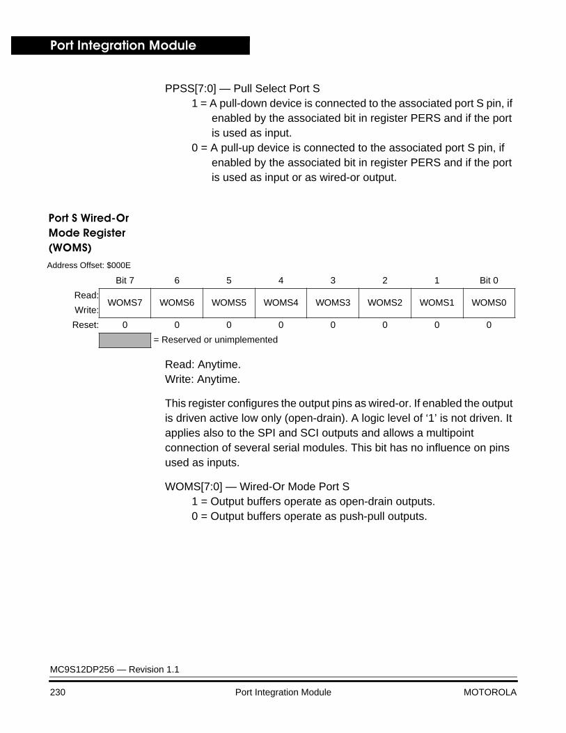
Port Integration Module
MC9S12DP256 — Revision 1.1
230 Port Integration Module MOTOROLA
PPSS[7:0] — Pull Select Port S1 = A pull-down device is connected to the associated port S pin, if
enabled by the associated bit in register PERS and if the port is used as input.
0 = A pull-up device is connected to the associated port S pin, if enabled by the associated bit in register PERS and if the port is used as input or as wired-or output.
Port S Wired-Or Mode Register (WOMS)
Read: Anytime.Write: Anytime.
This register configures the output pins as wired-or. If enabled the output is driven active low only (open-drain). A logic level of ‘1’ is not driven. It applies also to the SPI and SCI outputs and allows a multipoint connection of several serial modules. This bit has no influence on pins used as inputs.
WOMS[7:0] — Wired-Or Mode Port S1 = Output buffers operate as open-drain outputs.0 = Output buffers operate as push-pull outputs.
Address Offset: $000E
Bit 7 6 5 4 3 2 1 Bit 0
Read:WOMS7 WOMS6 WOMS5 WOMS4 WOMS3 WOMS2 WOMS1 WOMS0
Write:
Reset: 0 0 0 0 0 0 0 0
= Reserved or unimplemented

Port Integration ModuleRegister Descriptions
MC9S12DP256 — Revision 1.1
MOTOROLA Port Integration Module 231
Port M I/ORegister (PTM)
Read: Anytime.Write: Anytime.
If the data direction bits of the associated I/O pins are set to 1, a read returns the value of the port register, otherwise the value at the pins is read. The CAN function (TxCAN and RxCAN) takes precedence over the general purpose I/O function if the associated CAN module is enabled. See MSCAN section. The BDLC function takes precedence over the general purpose I/O function associated with if enabled. See Byte Data Link Controller Module section.If both CAN0 and BDLC are enabled the CAN functionality takes precedence.
Port M Input Register (PTIM)
Read: Anytime.Write: Never; writes to this register have no effect.
Address Offset: $0010
Bit 7 6 5 4 3 2 1 Bit 0
Read:PTM7 PTM6 PTM5 PTM4 PTM3 PTM2 PTM1 PTM0
Write:
CAN: TxCAN3 RxCAN3 TxCAN2 RxCAN2 TxCAN1 RxCAN1 TxCAN0 RxCAN0
J1850: TxBDLC RxBDLC
Reset: 0 0 0 0 0 0 0 0
= Reserved or unimplemented
Address Offset: $0011
Bit 7 6 5 4 3 2 1 Bit 0
Read: PTIM7 PTIM6 PTIM5 PTIM4 PTIM3 PTIM2 PTIM1 PTIM0
Write:
Reset: - - - - - - - -
= Reserved or unimplemented
Port Integration Module
MC9S12DP256 — Revision 1.1
232 Port Integration Module MOTOROLA
This register always reads back the status of the associated pins. This can also be used to detect overload or short circuit conditions on output pins.
Port M Data Direction Register (DDRM)
Read: Anytime.Write: Anytime.
This register configures each port M pin as either input or output.The CAN/BDLC forces the I/O state to be an output for each port line associated with an enabled output (TxCAN[3:0], TxBDLC). It also forces the I/O state to be an input for each port line associated with an enabled input (RxCAN[3:0], RxBDLC). In those cases the data direction bits will not change. The DDRM bits revert to controlling the I/O direction of a pin when the associated peripheral module is disabled.
DDRM[7:0] — Data Direction Port M1 = Associated pin is configured as output.0 = Associated pin is configured as input.
Due to internal synchronization circuits, it can take up to 2 bus cycles until the correct value is read on PTM or PTIM registers, when changing the DDRM register.
Address Offset: $0012
Bit 7 6 5 4 3 2 1 Bit 0
Read:DDRM7 DDRM6 DDRM5 DDRM4 DDRM3 DDRM2 DDRM1 DDRM0
Write:
Reset: 0 0 0 0 0 0 0 0
= Reserved or unimplemented
Port Integration ModuleRegister Descriptions
MC9S12DP256 — Revision 1.1
MOTOROLA Port Integration Module 233
Port M Reduced Drive Register (RDRM)
Read: Anytime.Write: Anytime.
This register configures the drive strength of each port M output pin as either full or reduced. If the port is used as input this bit is ignored.
RDRM[7:0] — Reduced Drive Port M1 = Associated pin drives at about 1/3 of the full drive strength.0 = Full drive strength at output.
Port M Pull Device Enable Register (PERM)
Read: Anytime.Write: Anytime.
This register configures whether a pull-up or a pull-down device is activated, if the port is used as input or wired-or output. This bit has no effect if the port is used as push-pull output. Out of reset no pull device is enabled.
Address Offset: $0013
Bit 7 6 5 4 3 2 1 Bit 0
Read:RDRM7 RDRM6 RDRM5 RDRM4 RDRM3 RDRM2 RDRM1 RDRM0
Write:
Reset: 0 0 0 0 0 0 0 0
= Reserved or unimplemented
Address Offset: $0014
Bit 7 6 5 4 3 2 1 Bit 0
Read:PERM7 PERM6 PERM5 PERM4 PERM3 PERM2 PERM1 PERM0
Write:
Reset: 0 0 0 0 0 0 0 0
= Reserved or unimplemented
Port Integration Module
MC9S12DP256 — Revision 1.1
234 Port Integration Module MOTOROLA
PERM[7:0] — Pull Device Enable Port M1 = Either a pull-up or pull-down device is enabled.0 = Pull-up or pull-down device is disabled.
Port M Polarity Select Register (PPSM)
Read: Anytime.Write: Anytime.
This register selects whether a pull-down or a pull-up device is connected to the pin. If CAN is active a pull-up device can be activated on the RxCAN[3:0] inputs, but not a pull-down. If BDLC is active a pull-down device can be activated on the RxBDLC pin but not a pull-up.
PPSM[7:0] — Pull Select Port M1 = A pull-down device is connected to the associated port M pin,
if enabled by the associated bit in register PERM and if the port is used as a general purpose or BDLC input but not as RxCAN.
0 = A pull-up device is connected to the associated port M pin, if enabled by the associated bit in register PERM and if the port is used as general purpose or RxCAN input but not as BDLC.
Address Offset: $0015
Bit 7 6 5 4 3 2 1 Bit 0
Read:PPSM7 PPSM6 PPSM5 PPSM4 PPSM3 PPSM2 PPSM1 PPSM0
Write:
Reset: 0 0 0 0 0 0 0 0
= Reserved or unimplemented
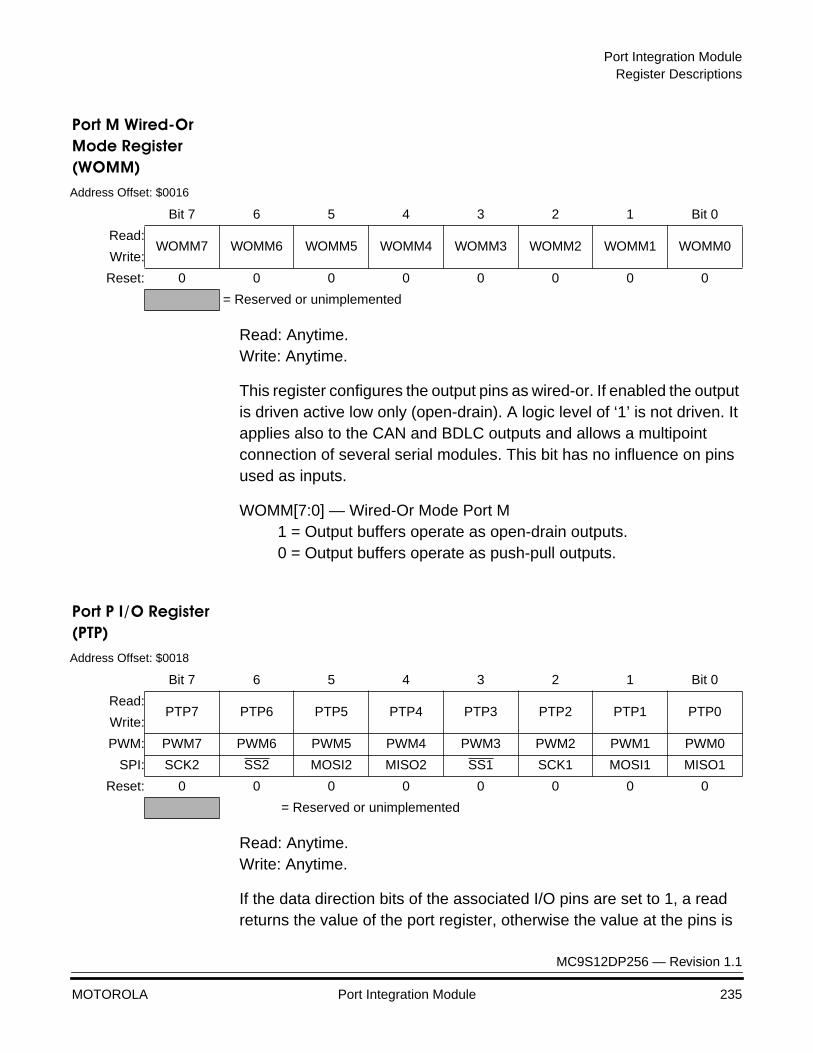
Port Integration ModuleRegister Descriptions
MC9S12DP256 — Revision 1.1
MOTOROLA Port Integration Module 235
Port M Wired-Or Mode Register (WOMM)
Read: Anytime.Write: Anytime.
This register configures the output pins as wired-or. If enabled the output is driven active low only (open-drain). A logic level of ‘1’ is not driven. It applies also to the CAN and BDLC outputs and allows a multipoint connection of several serial modules. This bit has no influence on pins used as inputs.
WOMM[7:0] — Wired-Or Mode Port M1 = Output buffers operate as open-drain outputs.0 = Output buffers operate as push-pull outputs.
Port P I/O Register (PTP)
Read: Anytime.Write: Anytime.
If the data direction bits of the associated I/O pins are set to 1, a read returns the value of the port register, otherwise the value at the pins is
Address Offset: $0016
Bit 7 6 5 4 3 2 1 Bit 0
Read:WOMM7 WOMM6 WOMM5 WOMM4 WOMM3 WOMM2 WOMM1 WOMM0
Write:
Reset: 0 0 0 0 0 0 0 0
= Reserved or unimplemented
Address Offset: $0018
Bit 7 6 5 4 3 2 1 Bit 0
Read:PTP7 PTP6 PTP5 PTP4 PTP3 PTP2 PTP1 PTP0
Write:
PWM: PWM7 PWM6 PWM5 PWM4 PWM3 PWM2 PWM1 PWM0
SPI: SCK2 SS2 MOSI2 MISO2 SS1 SCK1 MOSI1 MISO1
Reset: 0 0 0 0 0 0 0 0
= Reserved or unimplemented
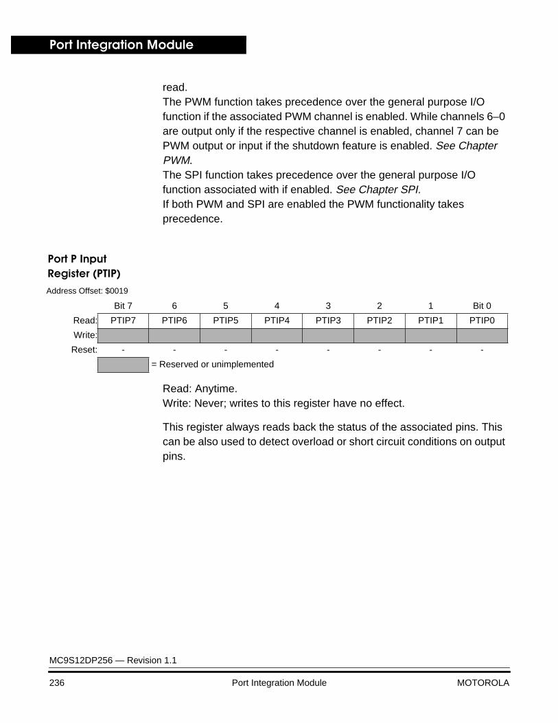
Port Integration Module
MC9S12DP256 — Revision 1.1
236 Port Integration Module MOTOROLA
read. The PWM function takes precedence over the general purpose I/O function if the associated PWM channel is enabled. While channels 6–0 are output only if the respective channel is enabled, channel 7 can be PWM output or input if the shutdown feature is enabled. See Chapter PWM. The SPI function takes precedence over the general purpose I/O function associated with if enabled. See Chapter SPI.If both PWM and SPI are enabled the PWM functionality takes precedence.
Port P Input Register (PTIP)
Read: Anytime.Write: Never; writes to this register have no effect.
This register always reads back the status of the associated pins. This can be also used to detect overload or short circuit conditions on output pins.
Address Offset: $0019
Bit 7 6 5 4 3 2 1 Bit 0
Read: PTIP7 PTIP6 PTIP5 PTIP4 PTIP3 PTIP2 PTIP1 PTIP0
Write:
Reset: - - - - - - - -
= Reserved or unimplemented
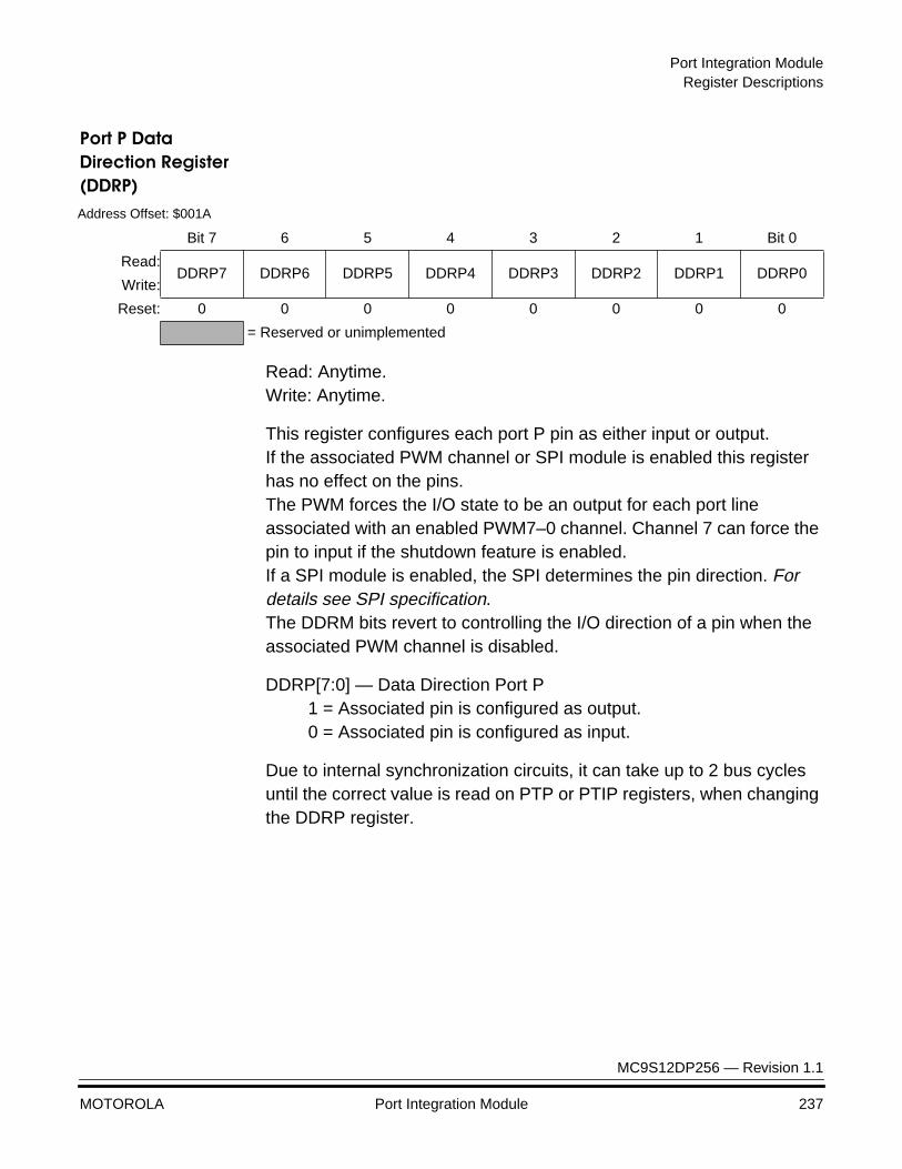
Port Integration ModuleRegister Descriptions
MC9S12DP256 — Revision 1.1
MOTOROLA Port Integration Module 237
Port P Data Direction Register (DDRP)
Read: Anytime.Write: Anytime.
This register configures each port P pin as either input or output.If the associated PWM channel or SPI module is enabled this register has no effect on the pins. The PWM forces the I/O state to be an output for each port line associated with an enabled PWM7–0 channel. Channel 7 can force the pin to input if the shutdown feature is enabled. If a SPI module is enabled, the SPI determines the pin direction. For details see SPI specification. The DDRM bits revert to controlling the I/O direction of a pin when the associated PWM channel is disabled.
DDRP[7:0] — Data Direction Port P1 = Associated pin is configured as output.0 = Associated pin is configured as input.
Due to internal synchronization circuits, it can take up to 2 bus cycles until the correct value is read on PTP or PTIP registers, when changing the DDRP register.
Address Offset: $001A
Bit 7 6 5 4 3 2 1 Bit 0
Read:DDRP7 DDRP6 DDRP5 DDRP4 DDRP3 DDRP2 DDRP1 DDRP0
Write:
Reset: 0 0 0 0 0 0 0 0
= Reserved or unimplemented
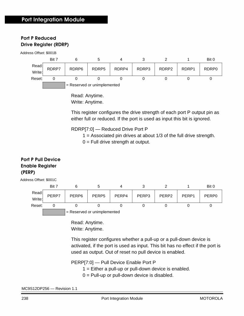
Port Integration Module
MC9S12DP256 — Revision 1.1
238 Port Integration Module MOTOROLA
Port P ReducedDrive Register (RDRP)
Read: Anytime.Write: Anytime.
This register configures the drive strength of each port P output pin as either full or reduced. If the port is used as input this bit is ignored.
RDRP[7:0] — Reduced Drive Port P1 = Associated pin drives at about 1/3 of the full drive strength.0 = Full drive strength at output.
Port P Pull Device Enable Register (PERP)
Read: Anytime.Write: Anytime.
This register configures whether a pull-up or a pull-down device is activated, if the port is used as input. This bit has no effect if the port is used as output. Out of reset no pull device is enabled.
PERP[7:0] — Pull Device Enable Port P1 = Either a pull-up or pull-down device is enabled.0 = Pull-up or pull-down device is disabled.
Address Offset: $001B
Bit 7 6 5 4 3 2 1 Bit 0
Read:RDRP7 RDRP6 RDRP5 RDRP4 RDRP3 RDRP2 RDRP1 RDRP0
Write:
Reset: 0 0 0 0 0 0 0 0
= Reserved or unimplemented
Address Offset: $001C
Bit 7 6 5 4 3 2 1 Bit 0
Read:PERP7 PERP6 PERP5 PERP4 PERP3 PERP2 PERP1 PERP0
Write:
Reset: 0 0 0 0 0 0 0 0
= Reserved or unimplemented
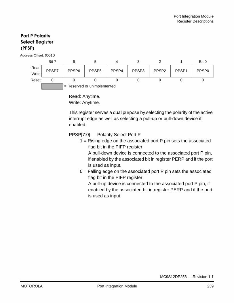
Port Integration ModuleRegister Descriptions
MC9S12DP256 — Revision 1.1
MOTOROLA Port Integration Module 239
Port P Polarity Select Register (PPSP)
Read: Anytime.Write: Anytime.
This register serves a dual purpose by selecting the polarity of the active interrupt edge as well as selecting a pull-up or pull-down device if enabled.
PPSP[7:0] — Polarity Select Port P1 = Rising edge on the associated port P pin sets the associated
flag bit in the PIFP register.A pull-down device is connected to the associated port P pin, if enabled by the associated bit in register PERP and if the port is used as input.
0 = Falling edge on the associated port P pin sets the associated flag bit in the PIFP register.A pull-up device is connected to the associated port P pin, if enabled by the associated bit in register PERP and if the port is used as input.
Address Offset: $001D
Bit 7 6 5 4 3 2 1 Bit 0
Read:PPSP7 PPSP6 PPSP5 PPSP4 PPSP3 PPSP2 PPSP1 PPSP0
Write:
Reset: 0 0 0 0 0 0 0 0
= Reserved or unimplemented
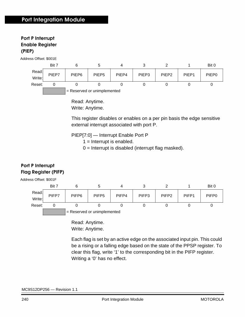
Port Integration Module
MC9S12DP256 — Revision 1.1
240 Port Integration Module MOTOROLA
Port P Interrupt Enable Register (PIEP)
Read: Anytime.Write: Anytime.
This register disables or enables on a per pin basis the edge sensitive external interrupt associated with port P.
PIEP[7:0] — Interrupt Enable Port P1 = Interrupt is enabled.0 = Interrupt is disabled (interrupt flag masked).
Port P Interrupt Flag Register (PIFP)
Read: Anytime.Write: Anytime.
Each flag is set by an active edge on the associated input pin. This could be a rising or a falling edge based on the state of the PPSP register. To clear this flag, write ‘1’ to the corresponding bit in the PIFP register. Writing a ‘0’ has no effect.
Address Offset: $001E
Bit 7 6 5 4 3 2 1 Bit 0
Read:PIEP7 PIEP6 PIEP5 PIEP4 PIEP3 PIEP2 PIEP1 PIEP0
Write:
Reset: 0 0 0 0 0 0 0 0
= Reserved or unimplemented
Address Offset: $001F
Bit 7 6 5 4 3 2 1 Bit 0
Read:PIFP7 PIFP6 PIFP5 PIFP4 PIFP3 PIFP2 PIFP1 PIFP0
Write:
Reset: 0 0 0 0 0 0 0 0
= Reserved or unimplemented
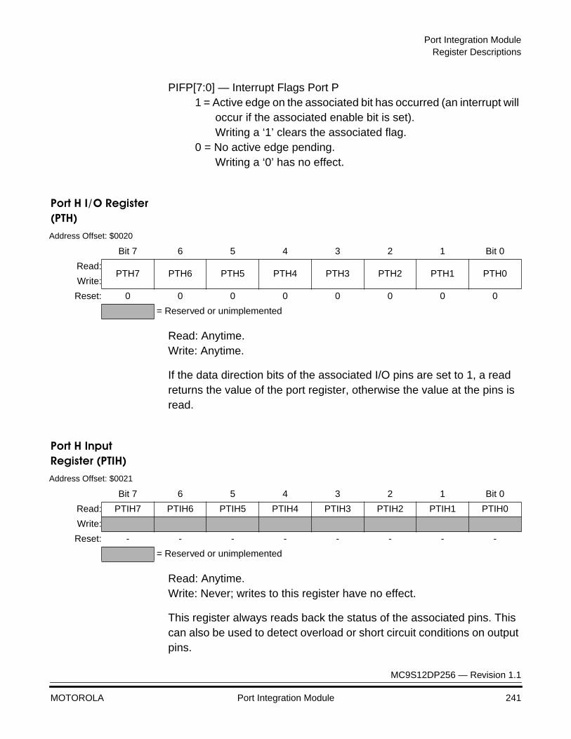
Port Integration ModuleRegister Descriptions
MC9S12DP256 — Revision 1.1
MOTOROLA Port Integration Module 241
PIFP[7:0] — Interrupt Flags Port P1 = Active edge on the associated bit has occurred (an interrupt will
occur if the associated enable bit is set).Writing a ‘1’ clears the associated flag.
0 = No active edge pending.Writing a ‘0’ has no effect.
Port H I/O Register (PTH)
Read: Anytime.Write: Anytime.
If the data direction bits of the associated I/O pins are set to 1, a read returns the value of the port register, otherwise the value at the pins is read.
Port H Input Register (PTIH)
Read: Anytime.Write: Never; writes to this register have no effect.
This register always reads back the status of the associated pins. This can also be used to detect overload or short circuit conditions on output pins.
Address Offset: $0020
Bit 7 6 5 4 3 2 1 Bit 0
Read:PTH7 PTH6 PTH5 PTH4 PTH3 PTH2 PTH1 PTH0
Write:
Reset: 0 0 0 0 0 0 0 0
= Reserved or unimplemented
Address Offset: $0021
Bit 7 6 5 4 3 2 1 Bit 0
Read: PTIH7 PTIH6 PTIH5 PTIH4 PTIH3 PTIH2 PTIH1 PTIH0
Write:
Reset: - - - - - - - -
= Reserved or unimplemented
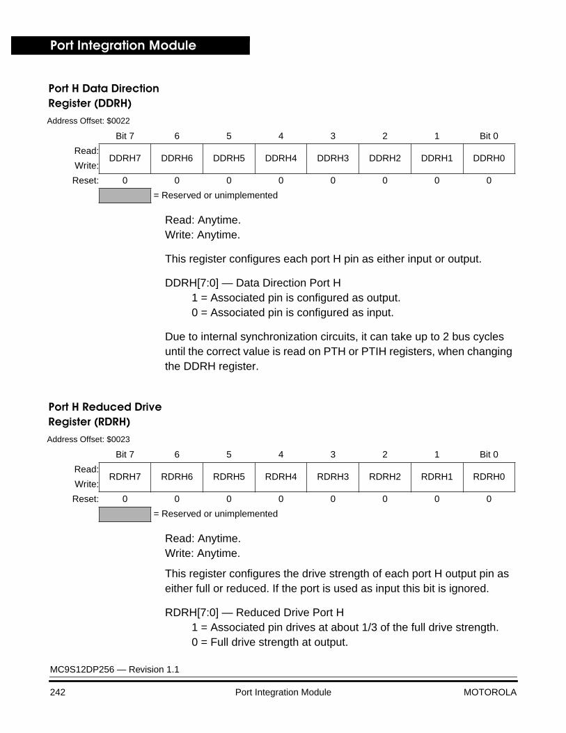
Port Integration Module
MC9S12DP256 — Revision 1.1
242 Port Integration Module MOTOROLA
Port H Data DirectionRegister (DDRH)
Read: Anytime.Write: Anytime.
This register configures each port H pin as either input or output.
DDRH[7:0] — Data Direction Port H1 = Associated pin is configured as output.0 = Associated pin is configured as input.
Due to internal synchronization circuits, it can take up to 2 bus cycles until the correct value is read on PTH or PTIH registers, when changing the DDRH register.
Port H Reduced DriveRegister (RDRH)
Read: Anytime.Write: Anytime.
This register configures the drive strength of each port H output pin as either full or reduced. If the port is used as input this bit is ignored.
RDRH[7:0] — Reduced Drive Port H1 = Associated pin drives at about 1/3 of the full drive strength.0 = Full drive strength at output.
Address Offset: $0022
Bit 7 6 5 4 3 2 1 Bit 0
Read:DDRH7 DDRH6 DDRH5 DDRH4 DDRH3 DDRH2 DDRH1 DDRH0
Write:
Reset: 0 0 0 0 0 0 0 0
= Reserved or unimplemented
Address Offset: $0023
Bit 7 6 5 4 3 2 1 Bit 0
Read:RDRH7 RDRH6 RDRH5 RDRH4 RDRH3 RDRH2 RDRH1 RDRH0
Write:
Reset: 0 0 0 0 0 0 0 0
= Reserved or unimplemented
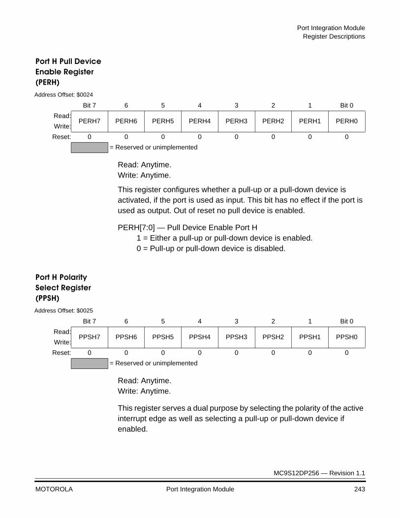
Port Integration ModuleRegister Descriptions
MC9S12DP256 — Revision 1.1
MOTOROLA Port Integration Module 243
Port H Pull Device Enable Register (PERH)
Read: Anytime.Write: Anytime.
This register configures whether a pull-up or a pull-down device is activated, if the port is used as input. This bit has no effect if the port is used as output. Out of reset no pull device is enabled.
PERH[7:0] — Pull Device Enable Port H1 = Either a pull-up or pull-down device is enabled.0 = Pull-up or pull-down device is disabled.
Port H Polarity Select Register (PPSH)
Read: Anytime.Write: Anytime.
This register serves a dual purpose by selecting the polarity of the active interrupt edge as well as selecting a pull-up or pull-down device if enabled.
Address Offset: $0024
Bit 7 6 5 4 3 2 1 Bit 0
Read:PERH7 PERH6 PERH5 PERH4 PERH3 PERH2 PERH1 PERH0
Write:
Reset: 0 0 0 0 0 0 0 0
= Reserved or unimplemented
Address Offset: $0025
Bit 7 6 5 4 3 2 1 Bit 0
Read:PPSH7 PPSH6 PPSH5 PPSH4 PPSH3 PPSH2 PPSH1 PPSH0
Write:
Reset: 0 0 0 0 0 0 0 0
= Reserved or unimplemented
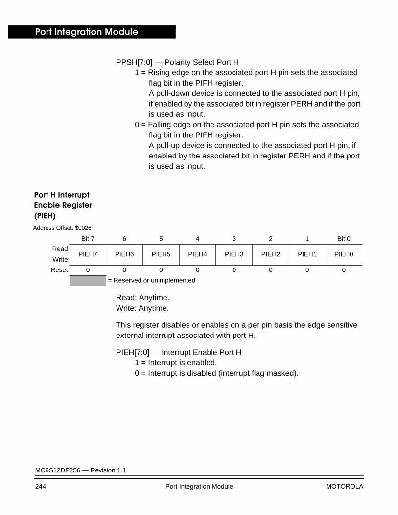
Port Integration Module
MC9S12DP256 — Revision 1.1
244 Port Integration Module MOTOROLA
PPSH[7:0] — Polarity Select Port H1 = Rising edge on the associated port H pin sets the associated
flag bit in the PIFH register.A pull-down device is connected to the associated port H pin, if enabled by the associated bit in register PERH and if the port is used as input.
0 = Falling edge on the associated port H pin sets the associated flag bit in the PIFH register.A pull-up device is connected to the associated port H pin, if enabled by the associated bit in register PERH and if the port is used as input.
Port H Interrupt Enable Register (PIEH)
Read: Anytime.Write: Anytime.
This register disables or enables on a per pin basis the edge sensitive external interrupt associated with port H.
PIEH[7:0] — Interrupt Enable Port H1 = Interrupt is enabled.0 = Interrupt is disabled (interrupt flag masked).
Address Offset: $0026
Bit 7 6 5 4 3 2 1 Bit 0
Read:PIEH7 PIEH6 PIEH5 PIEH4 PIEH3 PIEH2 PIEH1 PIEH0
Write:
Reset: 0 0 0 0 0 0 0 0
= Reserved or unimplemented
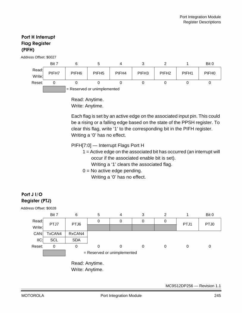
Port Integration ModuleRegister Descriptions
MC9S12DP256 — Revision 1.1
MOTOROLA Port Integration Module 245
Port H Interrupt Flag Register (PIFH)
Read: Anytime.Write: Anytime.
Each flag is set by an active edge on the associated input pin. This could be a rising or a falling edge based on the state of the PPSH register. To clear this flag, write ‘1’ to the corresponding bit in the PIFH register. Writing a ‘0’ has no effect.
PIFH[7:0] — Interrupt Flags Port H1 = Active edge on the associated bit has occurred (an interrupt will
occur if the associated enable bit is set).Writing a ‘1’ clears the associated flag.
0 = No active edge pending.Writing a ‘0’ has no effect.
Port J I/ORegister (PTJ)
Read: Anytime.Write: Anytime.
Address Offset: $0027
Bit 7 6 5 4 3 2 1 Bit 0
Read:PIFH7 PIFH6 PIFH5 PIFH4 PIFH3 PIFH2 PIFH1 PIFH0
Write:
Reset: 0 0 0 0 0 0 0 0
= Reserved or unimplemented
Address Offset: $0028
Bit 7 6 5 4 3 2 1 Bit 0
Read:PTJ7 PTJ6
0 0 0 0PTJ1 PTJ0
Write:
CAN: TxCAN4 RxCAN4
IIC: SCL SDA
Reset: 0 0 0 0 0 0 0 0
= Reserved or unimplemented

Port Integration Module
MC9S12DP256 — Revision 1.1
246 Port Integration Module MOTOROLA
If the data direction bits of the associated I/O pins are set to 1, a read returns the value of the port register, otherwise the value at the pins is read. The CAN function (TxCAN and RxCAN) takes precedence over the general purpose I/O function if the associated CAN module is enabled. See Chapter CAN. The IIC function takes precedence over the general purpose I/O function associated with if enabled. If both CAN4 and IIC are enabled the CAN functionality takes precedence. See Chapter IIC. If the IIC module is enabled the SDA and SCL outputs are configured as open-drain outputs.
Port J Input Register (PTIJ)
Read: Anytime.Write: Never; writes to this register have no effect.
This register always reads back the status of the associated pins. This can be used to detect overload or short circuit conditions on output pins.
Address Offset: $0029
Bit 7 6 5 4 3 2 1 Bit 0
Read: PTIJ7 PTIJ6 0 0 0 0 PTIJ1 PTIJ0
Write:
Reset: – – 0 0 0 0 - –
= Reserved or unimplemented

Port Integration ModuleRegister Descriptions
MC9S12DP256 — Revision 1.1
MOTOROLA Port Integration Module 247
Port J Data Direction Register (DDRJ)
Read: Anytime.Write: Anytime.
This register configures each port J pin as either input or output.The CAN forces the I/O state to be an output on PJ7 (TxCAN4) and an input on pin PJ6 (RxCAN4). The IIC forces the I/O state to be an output or input dependent on the state of the IIC bus if enabled. In these cases the data direction bits will not change. The DDRJ bits revert to controlling the I/O direction of a pin when the associated timer output compare is disabled.
DDRJ[7:6][1:0] — Data Direction Port J1 = Associated pin is configured as output.0 = Associated pin is configured as input.
Due to internal synchronization circuits, it can take up to 2 bus cycles until the correct value is read on PTJ or PTIJ registers, when changing the DDRJ register.
Address Offset: $002A
Bit 7 6 5 4 3 2 1 Bit 0
Read:DDRJ7 DDRJ6
0 0 0 0DDRJ1 DDRJ0
Write:
Reset: 0 0 –f –f –f –f 0 0
= Reserved or unimplemented

Port Integration Module
MC9S12DP256 — Revision 1.1
248 Port Integration Module MOTOROLA
Port J Reduced DriveRegister (RDRJ)
Read: Anytime.Write: Anytime.
This register configures the drive strength of each port J output pin as either full or reduced. If the port is used as input this bit is ignored.
RDRJ[7:6][1:0] — Reduced Drive Port J1 = Associated pin drives at about 1/3 of the full drive strength.0 = Full drive strength at output.
Port J Pull Device Enable Register (PERJ)
Read: Anytime.Write: Anytime.
This register configures whether a pull-up or a pull-down device is activated, if the port is used as input or as wired-or output. This bit has no effect if the port is used as push-pull output. Out of reset a pull-up device is enabled.
PERJ[7:6][1:0] — Pull Device Enable Port J1 = Either a pull-up or pull-down device is enabled.0 = Pull-up or pull-down device is disabled.
Address Offset: $002B
Bit 7 6 5 4 3 2 1 Bit 0
Read:RDRJ7 RDRJ6
0 0 0 0RDRJ1 RDRJ0
Write:
Reset: 0 0 0 0 0 0 0 0
= Reserved or unimplemented
Address Offset: $002C
Bit 7 6 5 4 3 2 1 Bit 0
Read:PERJ7 PERJ6
0 0 0 0PERJ1 PERJ0
Write:
Reset: 1 1 0 0 0 0 1 1
= Reserved or unimplemented
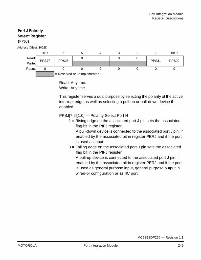
Port Integration ModuleRegister Descriptions
MC9S12DP256 — Revision 1.1
MOTOROLA Port Integration Module 249
Port J Polarity Select Register (PPSJ)
Read: Anytime.Write: Anytime.
This register serves a dual purpose by selecting the polarity of the active interrupt edge as well as selecting a pull-up or pull-down device if enabled.
PPSJ[7:6][1:0] — Polarity Select Port H1 = Rising edge on the associated port J pin sets the associated
flag bit in the PIFJ register.A pull-down device is connected to the associated port J pin, if enabled by the associated bit in register PERJ and if the port is used as input.
0 = Falling edge on the associated port J pin sets the associated flag bit in the PIFJ register.A pull-up device is connected to the associated port J pin, if enabled by the associated bit in register PERJ and if the port is used as general purpose input, general purpose output in wired-or configuration or as IIC port.
Address Offset: $002D
Bit 7 6 5 4 3 2 1 Bit 0
Read:PPSJ7 PPSJ6
0 0 0 0PPSJ1 PPSJ0
Write:
Reset: 0 0 0 0 0 0 0 0
= Reserved or unimplemented
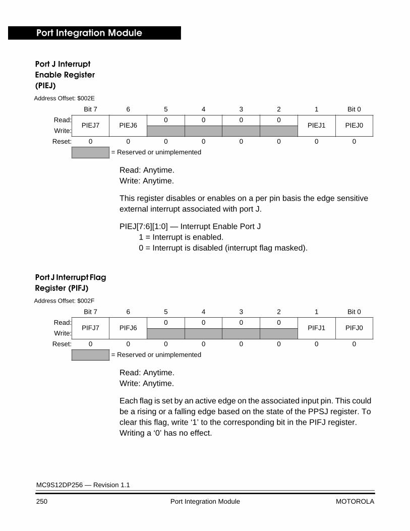
Port Integration Module
MC9S12DP256 — Revision 1.1
250 Port Integration Module MOTOROLA
Port J Interrupt Enable Register (PIEJ)
Read: Anytime.Write: Anytime.
This register disables or enables on a per pin basis the edge sensitive external interrupt associated with port J.
PIEJ[7:6][1:0] — Interrupt Enable Port J1 = Interrupt is enabled.0 = Interrupt is disabled (interrupt flag masked).
Port J Interrupt Flag Register (PIFJ)
Read: Anytime.Write: Anytime.
Each flag is set by an active edge on the associated input pin. This could be a rising or a falling edge based on the state of the PPSJ register. To clear this flag, write ‘1’ to the corresponding bit in the PIFJ register. Writing a ‘0’ has no effect.
Address Offset: $002E
Bit 7 6 5 4 3 2 1 Bit 0
Read:PIEJ7 PIEJ6
0 0 0 0PIEJ1 PIEJ0
Write:
Reset: 0 0 0 0 0 0 0 0
= Reserved or unimplemented
Address Offset: $002F
Bit 7 6 5 4 3 2 1 Bit 0
Read:PIFJ7 PIFJ6
0 0 0 0PIFJ1 PIFJ0
Write:
Reset: 0 0 0 0 0 0 0 0
= Reserved or unimplemented
Port Integration ModuleReset Initialization
MC9S12DP256 — Revision 1.1
MOTOROLA Port Integration Module 251
PIFH[7:6][1:0] — Interrupt Flags Port J1 = Active edge on the associated bit has occurred (an interrupt will
occur if the associated enable bit is set).Writing a ‘1’ clears the associated flag.
0 = No active edge pending.Writing a ‘0’ has no effect.
Reset Initialization
All registers including the data registers get set/reset asynchronously.
Functional Description
General Each pin can act as general purpose I/O. In addition the pin can act as an output from a peripheral module or an input to a peripheral module. A set of configuration registers is common to all ports. All registers can be written at any time, however a specific configuration might not become active.
Example:
Selecting a pull-up resistor. This resistor does not become active while the port is used as a push-pull output.
I/O register This register holds the value driven out to the pin if the port is used as a general purpose I/O. Writing to this register has only an effect on the pin if the port is used as general purpose output. When reading this address, the value of the pins is returned if the data direction register bits are set to 0. If the data direction register bits are set to 1, the contents of the I/O register is returned. This is independent of any other configuration.
Input register This is a read-only register and always returns the value of the pin.
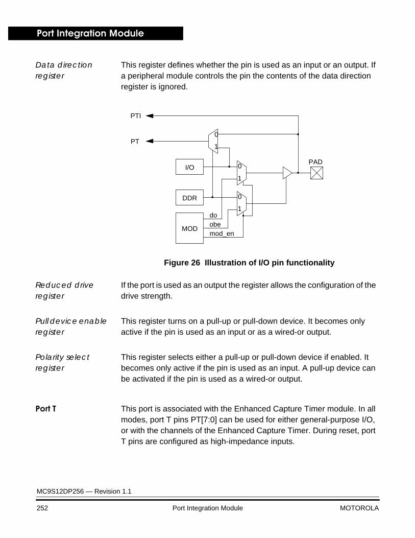
Port Integration Module
MC9S12DP256 — Revision 1.1
252 Port Integration Module MOTOROLA
Data direction register
This register defines whether the pin is used as an input or an output. If a peripheral module controls the pin the contents of the data direction register is ignored.
Figure 26 Illustration of I/O pin functionality
Reduced drive register
If the port is used as an output the register allows the configuration of the drive strength.
Pull device enable register
This register turns on a pull-up or pull-down device. It becomes only active if the pin is used as an input or as a wired-or output.
Polarity select register
This register selects either a pull-up or pull-down device if enabled. It becomes only active if the pin is used as an input. A pull-up device can be activated if the pin is used as a wired-or output.
Port T This port is associated with the Enhanced Capture Timer module. In all modes, port T pins PT[7:0] can be used for either general-purpose I/O, or with the channels of the Enhanced Capture Timer. During reset, port T pins are configured as high-impedance inputs.
I/O
DDR
MOD
doobemod_en
PT
PTI
1
0
1
1
0
0
PAD
Port Integration ModuleFunctional Description
MC9S12DP256 — Revision 1.1
MOTOROLA Port Integration Module 253
Port S This port is associated with the serial SCI and SPI modules. In all modes, port S pins PS[7:0] can be used either for general-purpose I/O, or with the SCI and SPI subsystems. During reset, port S pins are configured as inputs with pull-up.
Port M This port is associated with the J1850 and 4 CAN modules. In all modes, port M pins PM[7:0] can be used for either general purpose I/O, or with the CAN and J1850 subsystems. Pins PM0 and PM1 are shared between the CAN0 and the BDLC (J1850) module. If CAN0 is enabled the pins become CAN transmit and receive pins. If BLDC is enabled and CAN0 is disabled, pins become active BDLC transmit and receive pins. During reset, port M pins are configured as high-impedance inputs.
Port P This port is associated with the PWM and 2 SPI modules. In all modes, port P pins PP[7:0] can be used for either general purpose I/O, or with the PWM and SPI subsystems. The pins are shared between the PWM channels and the SPI1 and SPI2 modules. If the PWM is enabled the pins become PWM output channels with the exception of pin 7 which can be PWM input or output. If SPI1 or SPI2 are enabled and PWM is disabled, the respective pin configuration is determined by several status bits in the SPI modules. During reset, port P pins are configured as high-impedance inputs.
Port P offers 8 I/O pins with edge triggered interrupt capability in wired-or fashion. The interrupt enable as well as the sensitivity to rising or falling edges can be individually configured on per pin basis. All 8 bits/pins share the same interrupt vector. Interrupts can be used with the pins configured as inputs or outputs.
An interrupt is generated when a bit in the port interrupt flag register and its corresponding port interrupt enable bit are both set.
This external interrupt feature is capable to wake up the CPU when it is in STOP or WAIT mode.
A digital filter on each pin prevents pulses shorter than a specified time from generating an interrupt (see Pulse Detection Criteria). Four
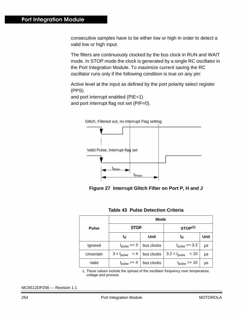
Port Integration Module
MC9S12DP256 — Revision 1.1
254 Port Integration Module MOTOROLA
consecutive samples have to be either low or high in order to detect a valid low or high input.
The filters are continuously clocked by the bus clock in RUN and WAIT mode. In STOP mode the clock is generated by a single RC oscillator in the Port Integration Module. To maximize current saving the RC oscillator runs only if the following condition is true on any pin:
Active level at the input as defined by the port polarity select register (PPS)and port interrupt enabled (PIE=1)and port interrupt flag not set (PIF=0).
Figure 27 Interrupt Glitch Filter on Port P, H and J
Table 43 Pulse Detection Criteria
Pulse
Mode
STOP STOP(1)
1. These values include the spread of the oscillator frequency over temperature,voltage and process.
tif Unit tif Unit
Ignored tpulse <= 3 bus clocks tpulse <= 3.2 µs
Uncertain 3 < tpulse < 4 bus clocks 3.2 < tpulse < 10 µs
Valid tpulse >= 4 bus clocks tpulse >= 10 µs
Glitch, Filtered out, no Interrupt Flag setting
Valid Pulse, Interrupt flag set
tifmin
tifmax
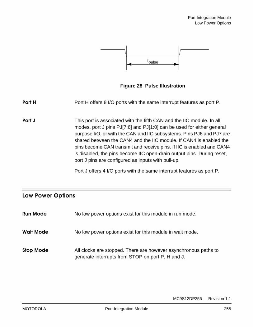
Port Integration ModuleLow Power Options
MC9S12DP256 — Revision 1.1
MOTOROLA Port Integration Module 255
Figure 28 Pulse Illustration
Port H Port H offers 8 I/O ports with the same interrupt features as port P.
Port J This port is associated with the fifth CAN and the IIC module. In all modes, port J pins PJ[7:6] and PJ[1:0] can be used for either general purpose I/O, or with the CAN and IIC subsystems. Pins PJ6 and PJ7 are shared between the CAN4 and the IIC module. If CAN4 is enabled the pins become CAN transmit and receive pins. If IIC is enabled and CAN4 is disabled, the pins become IIC open-drain output pins. During reset, port J pins are configured as inputs with pull-up.
Port J offers 4 I/O ports with the same interrupt features as port P.
Low Power Options
Run Mode No low power options exist for this module in run mode.
Wait Mode No low power options exist for this module in wait mode.
Stop Mode All clocks are stopped. There are however asynchronous paths to generate interrupts from STOP on port P, H and J.
tpulse
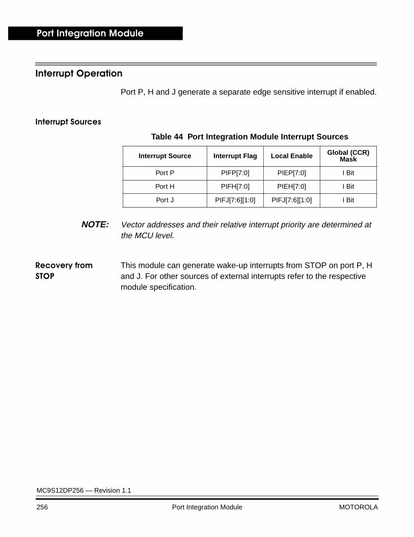
Port Integration Module
MC9S12DP256 — Revision 1.1
256 Port Integration Module MOTOROLA
Interrupt Operation
Port P, H and J generate a separate edge sensitive interrupt if enabled.
Interrupt Sources
NOTE: Vector addresses and their relative interrupt priority are determined at the MCU level.
Recovery from STOP
This module can generate wake-up interrupts from STOP on port P, H and J. For other sources of external interrupts refer to the respective module specification.
Table 44 Port Integration Module Interrupt Sources
Interrupt Source Interrupt Flag Local Enable Global (CCR) Mask
Port P PIFP[7:0] PIEP[7:0] I Bit
Port H PIFH[7:0] PIEH[7:0] I Bit
Port J PIFJ[7:6][1:0] PIFJ[7:6][1:0] I Bit
MC9S12DP256 — Revision 1.1
MOTOROLA Clocks and Reset Generator (CRG) 257
Clocks and Reset Generator (CRG)Clocks and Reset Generator (CRG)
Contents
Overview . . . . . . . . . . . . . . . . . . . . . . . . . . . . . . . . . . . . . . . . . . . . . . 257Features . . . . . . . . . . . . . . . . . . . . . . . . . . . . . . . . . . . . . . . . . . . . . . 258Block Diagram. . . . . . . . . . . . . . . . . . . . . . . . . . . . . . . . . . . . . . . . . . 259Register Map. . . . . . . . . . . . . . . . . . . . . . . . . . . . . . . . . . . . . . . . . . . 260Functional Description. . . . . . . . . . . . . . . . . . . . . . . . . . . . . . . . . . . . 261Register Descriptions . . . . . . . . . . . . . . . . . . . . . . . . . . . . . . . . . . . . 279External Pin Descriptions . . . . . . . . . . . . . . . . . . . . . . . . . . . . . . . . . 292Reset Initialization . . . . . . . . . . . . . . . . . . . . . . . . . . . . . . . . . . . . . . . 294Interrupt Operation . . . . . . . . . . . . . . . . . . . . . . . . . . . . . . . . . . . . . . 294Low Power Options . . . . . . . . . . . . . . . . . . . . . . . . . . . . . . . . . . . . . . 296
Overview
This specification describes the function of the Clocks and Reset Generator (CRG) and Oscillator (OSC) modules.
Clocks and Reset Generator (CRG)
MC9S12DP256 — Revision 1.1
258 Clocks and Reset Generator (CRG) MOTOROLA
Features
The main features of this block are:
• Crystal (or ceramic resonator) oscillator (OSC)
– Crystal Monitor (CM)
– Startup counter
• Phase Locked Loop (PLL) frequency multiplier
– Reference divider
– Automatic Bandwidth control mode for low-jitter operation
– Automatic Frequency lock detector
– CPU interrupt on Entry or Exit from Locked condition
– Self Clock mode in absence of reference clock
• System Clock Generator (CGEN)
– External Clock mode
– System clock switch
– System clocks off during WAIT mode
• System Reset Generator (RGEN)
– Computer Operating Properly (COP) Watchdog Timer with time-out clear window.
– Loss of crystal clock reset
– External pin reset
• Real-Time Interrupt (RTI)
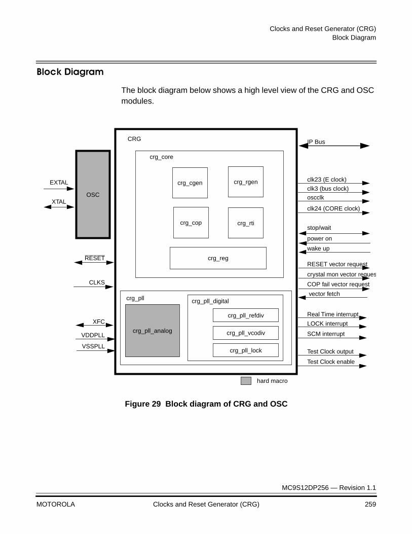
Clocks and Reset Generator (CRG)Block Diagram
MC9S12DP256 — Revision 1.1
MOTOROLA Clocks and Reset Generator (CRG) 259
Block Diagram
The block diagram below shows a high level view of the CRG and OSC modules.
Figure 29 Block diagram of CRG and OSC
CRG
crg_pll_analog
crg_pll_digital
crg_pll_refdiv
crg_pll_vcodiv
crg_pll_lock
crg_reg
crg_rti
crg_core
crg_cop
crg_rgencrg_cgen
OSC
crg_pll
hard macro
RESET
XFC
VSSPLL
VDDPLL
IP Bus
clk23 (E clock)
oscclk
stop/wait
power on
wake up
crystal mon vector reques
COP fail vector request
Real Time interrupt
clk24 (CORE clock)
LOCK interrupt
SCM interrupt
Test Clock output
Test Clock enable
RESET vector request
vector fetch
clk3 (bus clock)
XTAL
EXTAL
CLKS
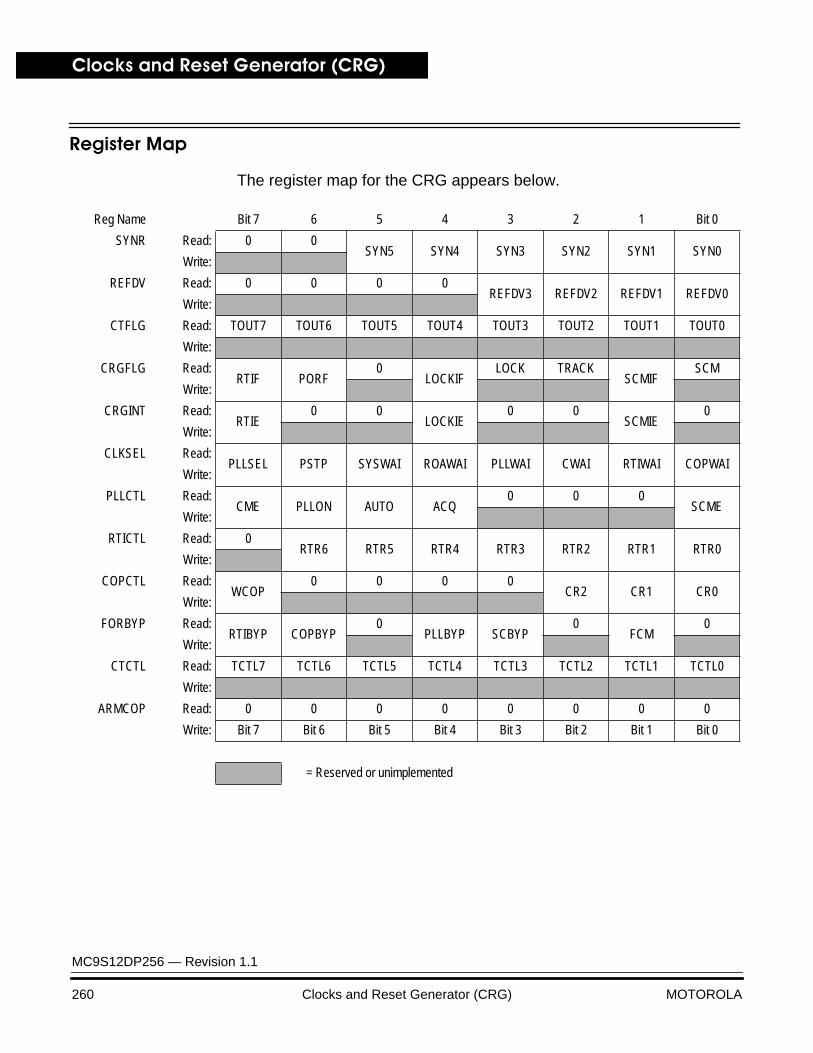
Clocks and Reset Generator (CRG)
MC9S12DP256 — Revision 1.1
260 Clocks and Reset Generator (CRG) MOTOROLA
Register Map
The register map for the CRG appears below.
Reg Name Bit 7 6 5 4 3 2 1 Bit 0
SYNR Read: 0 0SYN5 SYN4 SYN3 SYN2 SYN1 SYN0
Write:
REFDV Read: 0 0 0 0REFDV3 REFDV2 REFDV1 REFDV0
Write:
CTFLG Read: TOUT7 TOUT6 TOUT5 TOUT4 TOUT3 TOUT2 TOUT1 TOUT0
Write:
CRGFLG Read:RTIF PORF
0LOCKIF
LOCK TRACKSCMIF
SCM
Write:
CRGINT Read:RTIE
0 0LOCKIE
0 0SCMIE
0
Write:
CLKSEL Read:PLLSEL PSTP SYSWAI ROAWAI PLLWAI CWAI RTIWAI COPWAI
Write:
PLLCTL Read:CME PLLON AUTO ACQ
0 0 0SCME
Write:
RTICTL Read: 0RTR6 RTR5 RTR4 RTR3 RTR2 RTR1 RTR0
Write:
COPCTL Read:WCOP
0 0 0 0CR2 CR1 CR0
Write:
FORBYP Read:RTIBYP COPBYP
0PLLBYP SCBYP
0FCM
0
Write:
CTCTL Read: TCTL7 TCTL6 TCTL5 TCTL4 TCTL3 TCTL2 TCTL1 TCTL0
Write:
ARMCOP Read: 0 0 0 0 0 0 0 0
Write: Bit 7 Bit 6 Bit 5 Bit 4 Bit 3 Bit 2 Bit 1 Bit 0
= Reserved or unimplemented
Clocks and Reset Generator (CRG)Functional Description
MC9S12DP256 — Revision 1.1
MOTOROLA Clocks and Reset Generator (CRG) 261
NOTE: Register Address = Module Address + Base Address + Address Offset
The Module Address is determined at the MCU level.
The Address Offset is determined by a switch in the i/o of the module. If the switch is set, the address offset is four bytes, and if it is clear there is no offset.
Functional Description
Oscillator (OSC) The oscillator block has two external pins, EXTAL and XTAL. See Register Descriptions. The oscillator input pin, EXTAL, is intended to be connected to either a crystal or an external clock source. The XTAL pin is an output signal that provides crystal circuit feedback and can be buffered to drive other devices with same voltage amplitude. It is also used as an input pin during test when the MCU has an external clock source.
A buffered EXTAL signal, OSCCLK, becomes the internal reference clock. The oscillator is enabled based on the PSTP bit, and the STOP condition. The oscillator is disabled when the part is in STOP mode except when Pseudo-Stop mode is enabled. See Register Descriptions for detailed bit descriptions.
To improve noise immunity, the OSC is powered by the VDDPLL and VSSPLL power supply pins.
Table 45 CRG Register Address Summary
Register SYN REFDV CTFLG CRGFLG CRGINT CLKSEL
BaseAddress $0000 $0001 $0002 $0003 $0004 $0005
Register PLLCTL RTICTL COPCTL FORBYP CTCTL ARMCOP
BaseAddress $0006 $0007 $0008 $0009 $000A $000B
Clocks and Reset Generator (CRG)
MC9S12DP256 — Revision 1.1
262 Clocks and Reset Generator (CRG) MOTOROLA
The crystal oscillator is equipped with a feedback system which does not waste current generating harmonics. Its configuration is “Colpitts oscillator with translated ground”. The transconductor used is driven by a current source under the control of a peak detector which will measure the amplitude of the AC signal appearing on EXTAL node in order to implement an Amplitude Limitation Control (ALC) loop. The ALC loop is in charge of reducing the quiescent current in the transconductor as a result of an increase in the peak-to-peak oscillation amplitude.
Crystal Monitor (CM)
The crystal monitor circuit is based on an internal resistor-capacitor (RC) time delay so that it can operate without any MCU clocks. If no clock edges are detected within this RC time delay, the crystal monitor indicates failure which asserts self clock mode or generates a system reset depending on the state of SCME bit. If the crystal monitor is disabled or the presence of clocks are detected no failure is indicated.The crystal monitor function is enabled/disabled by the CME control bit. See Register Descriptions.
Startup counter The Startup Counter is a 14-stage ripple free-running counter that counts system clock cycles to ensure proper oscillator start up recovery. It is initialized at power on, stop mode, and any failure indicated by the crystal monitor when SCME bit is cleared. See Crystal loss, stop and startup for more information.
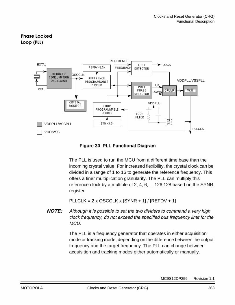
Clocks and Reset Generator (CRG)Functional Description
MC9S12DP256 — Revision 1.1
MOTOROLA Clocks and Reset Generator (CRG) 263
Phase Locked Loop (PLL)
Figure 30 PLL Functional Diagram
The PLL is used to run the MCU from a different time base than the incoming crystal value. For increased flexibility, the crystal clock can be divided in a range of 1 to 16 to generate the reference frequency. This offers a finer multiplication granularity. The PLL can multiply this reference clock by a multiple of 2, 4, 6, ... 126,128 based on the SYNR register.
PLLCLK = 2 x OSCCLK x [SYNR + 1] / [REFDV + 1]
NOTE: Although it is possible to set the two dividers to command a very high clock frequency, do not exceed the specified bus frequency limit for the MCU.
The PLL is a frequency generator that operates in either acquisition mode or tracking mode, depending on the difference between the output frequency and the target frequency. The PLL can change between acquisition and tracking modes either automatically or manually.
REDUCEDCONSUMPTION
OSCILLATOR
EXTAL
XTAL
OSCCLK
PLLCLK
REFERENCEPROGRAMMABLE
DIVIDER PDETPHASE
DETECTOR
REFDV <3:0>
LOOPPROGRAMMABLE
DIVIDER
SYN <5:0>
CPUMP VCO
LOCK
LOOPFILTER
XFCPAD
UP
DOWN
LOCKDETECTOR
REFERENCE
FEEDBACK
VDDPLL
VDDPLL/VSSPLL
CRYSTALMONITOR
VDDPLL/VSSPLL
VDD/VSS
Clocks and Reset Generator (CRG)
MC9S12DP256 — Revision 1.1
264 Clocks and Reset Generator (CRG) MOTOROLA
The VCO has a minimum operating frequency, which corresponds to the self clock mode frequency.
NOTE: Although it is possible to synthesize a PLLCLK frequency less than OSCCLK, some systems using a constant OSCCLK frequency base may not be able to operate.
PLL operation The OSCCLK input is fed through the reference programmable divider and is divided in a range of 1 to 16, [REFDV +1], to output the REFERENCE clock. The VCO output clock, PLLCLK, is fed back through the programmable loop divider and is divided in a range of 2 to 128 in increments of two, 2 x [SYNR +1], to output the FEEDBACK clock.See Figure 30.
The phase detector then compares the FEEDBACK clock, with the REFERENCE clock. Correction pulses are generated based on the phase difference between the two signals. The loop filter then slightly alters the D.C. voltage on the external filter connected to XFC pad, based on the width and direction of the correction pulse. The filter can make fast or slow corrections depending on its mode, described in Acquisition and tracking Modes below. The values of the external filter network and the reference frequency determines the speed of the corrections and the stability of the PLL.
Acquisition and tracking Modes
The lock detector compares the frequencies of the FEEDBACK clock, and the REFERENCE clock. Therefore, the speed of the lock detector is directly proportional to the final reference frequency. The circuit determines the mode of the PLL and the lock condition based on this comparison.
The PLL filter is manually or automatically configured into one of two operating modes:
Acquisition mode — In acquisition mode, the filter can make large frequency corrections to the VCO. This mode is used at PLL start-up or when the PLL has suffered a severe noise hit and the VCO frequency is far off the desired frequency. When in acquisition mode, the TRACK status bit is cleared in the CRGFLG register.

Clocks and Reset Generator (CRG)Functional Description
MC9S12DP256 — Revision 1.1
MOTOROLA Clocks and Reset Generator (CRG) 265
Tracking mode — In tracking mode, the filter makes only small corrections to the frequency of the VCO. PLL jitter is much lower in tracking mode, but the response to noise is also slower. The PLL enters tracking mode when the VCO frequency is nearly correct and the TRACK bit is set in the CRGFLG register.
The PLL can change the bandwidth or operational mode of the loop filter manually or automatically.
In automatic bandwidth control mode (AUTO = 1), the lock detector automatically switches between acquisition and tracking modes. Automatic bandwidth control mode also is used to determine when the PLL clock, PLLCLK, is safe to use as the source for the system clock, SYSCLK. If PLL LOCK interrupt requests are enabled, the software can wait for an interrupt request and then check the LOCK bit. If CPU interrupts are disabled, software can poll the LOCK bit continuously (during PLL start-up, usually) or at periodic intervals. In either case, only when the LOCK bit is set, is the PLLCLK clock safe to use as the source for the system clock. If the PLL is selected as the source for the system clock and the LOCK bit is clear, the PLL has suffered a severe noise hit and the software must take appropriate action, depending on the application.
The following conditions apply when the PLL is in automatic bandwidth control mode (AUTO=1):
• The TRACK bit is a read-only indicator of the mode of the filter.
• The TRACK bit is set when the VCO frequency is within a certain tolerance, ∆trk, and is clear when the VCO frequency is out of a certain tolerance, ∆unt.
• The LOCK bit is a read-only indicator of the locked state of the PLL.
• The LOCK bit is set when the VCO frequency is within a certain tolerance, ∆Lock, and is cleared when the VCO frequency is out of a certain tolerance, ∆unl.
• CPU interrupts can occur if enabled (LOCKIE = 1) when the lock condition changes, toggling the LOCK bit.

Clocks and Reset Generator (CRG)
MC9S12DP256 — Revision 1.1
266 Clocks and Reset Generator (CRG) MOTOROLA
The PLL also can operate in manual mode (AUTO = 0). Manual mode is used by systems that do not require an indicator of the lock condition for proper operation. Such systems typically operate well below the maximum system frequency, fsys, and require fast start-up. The following conditions apply when in manual mode:
• ACQ is a writable control bit that controls the mode of the filter. Before turning on the PLL in manual mode, the ACQ bit should be set to configure the filter in acquisition mode.
• Before entering tracking mode (ACQ = 0), software must wait a given time, tacq, after turning on the PLL by setting PLLON in the PLL control register, or wait until TRACK bit gets set.
• Software must wait a given time, tal, after entering tracking mode before selecting the PLLCLK as the SYSCLK clock source (PLLSEL = 1).
Self clock mode The VCO has a minimum operating frequency, fVCOMIN. If the crystal frequency is not available due to a failure or due to long crystal start-up time, the MCU system clock can be supplied by the VCO. This mode of operation is called Self-Clock mode. See Crystal loss, stop and startup for more information.
Crystal loss, stop and startup
The lack of external clocks can occur in three configurations, which are described below:
1. At Power-On Reset.
2. During normal clock operation.
3. In the STOP exit sequence.
Crystal startup at Power-On
Any reset sets the Crystal Monitor Enable bit, CME, the PLLON bit, and the self clock mode enable bit, SCME. Therefore, if the MCU is powered up without an external clock, self-clock mode is activated.
During a normal power up sequence without an external clock, after the POR pulse falling edge, the VCO supplies the self-clock mode frequency to the 14-stage Startup Counter as the output of the PLLSEL bit is forced
Clocks and Reset Generator (CRG)Functional Description
MC9S12DP256 — Revision 1.1
MOTOROLA Clocks and Reset Generator (CRG) 267
high. After the Startup Counter reaches the end of the count, 8192 self clock mode cycles, reset is released. At this time, if the crystal monitor indicates the presence of an external clock, self-clock mode is de-asserted and the MCU exits reset normally, using OSCCLK clock. In case the crystal start-up time is longer than the initial count of 8192 self clock mode cycles, or in the absence of an external clock, the MCU leaves the reset state in self-clock mode. Both SCM and SCMIF bits are set indicating the MCU is not operating at the desired frequency. Each time the Startup Counter reaches the end of the count, a check of the crystal monitor status is performed. When the presence of an external clock is detected, the SCM flag is cleared. This sets the self-clock interrupt flag and if enabled by the SCMIE bit, the self-clock mode interrupt is requested.
See Figure 31.
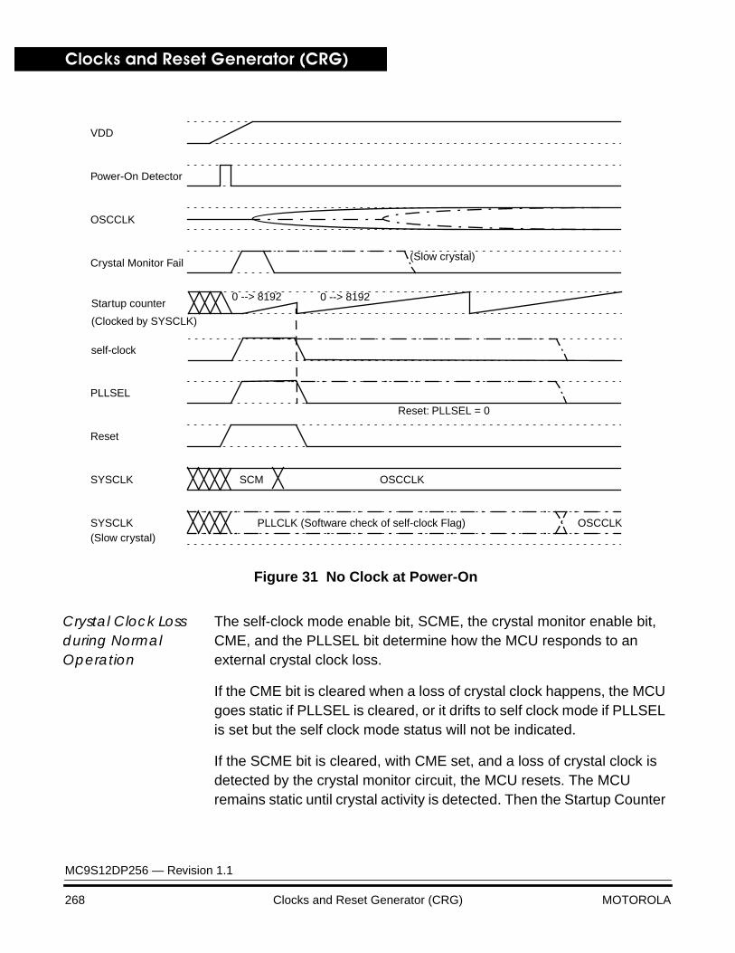
Clocks and Reset Generator (CRG)
MC9S12DP256 — Revision 1.1
268 Clocks and Reset Generator (CRG) MOTOROLA
Figure 31 No Clock at Power-On
Crystal Clock Loss during Normal Operation
The self-clock mode enable bit, SCME, the crystal monitor enable bit, CME, and the PLLSEL bit determine how the MCU responds to an external crystal clock loss.
If the CME bit is cleared when a loss of crystal clock happens, the MCU goes static if PLLSEL is cleared, or it drifts to self clock mode if PLLSEL is set but the self clock mode status will not be indicated.
If the SCME bit is cleared, with CME set, and a loss of crystal clock is detected by the crystal monitor circuit, the MCU resets. The MCU remains static until crystal activity is detected. Then the Startup Counter
self-clock
VDD
Power-On Detector
Crystal Monitor Fail
OSCCLK
Reset
PLLSEL
Reset: PLLSEL = 0
SYSCLK SCM OSCCLK
SYSCLK PLLCLK (Software check of self-clock Flag) OSCCLK(Slow crystal)
(Slow crystal)
Startup counter0 --> 8192
(Clocked by SYSCLK)
0 --> 8192
Clocks and Reset Generator (CRG)Functional Description
MC9S12DP256 — Revision 1.1
MOTOROLA Clocks and Reset Generator (CRG) 269
counts 8192 crystal clock cycles and at the end of the start up count the MCU completes its internal reset sequence.
If the SCME and CME bits are set, and a loss of crystal clock is detected by the crystal monitor circuit, the PLL VCO clock at its minimum frequency is provided as the system clock (self clock mode), allowing the MCU to continue operating. In self-clock mode, PLLON and PLLSEL outputs are forced high. The SCM flag in the CRGFLG register indicates that the MCU is running in self-clock mode. A change of this flag sets the self-clock interrupt flag and if enabled by the SCMIE bit, the self-clock mode interrupt is requested.
Each time the Startup Counter reaches the end of the count, a check of the crystal monitor status is performed. When the presence of an external clock is detected, the MCU leaves self-clock mode and the SCM flag is cleared. This also sets the self-clock interrupt flag. Upon leaving self-clock mode, PLLSEL is restored to its value before the crystal clock loss, and the system clock returns to its previous frequency. If AUTO and PLLSEL were set before the crystal clock loss, the system clock ramps-up and the PLL locks at the previously selected frequency. See Figure 32.
NOTE: There is a delay between the loss of crystal clock and its detection by the crystal monitor. If the MCU is clocked by OSCCLK and the PLL is not used there is a potential for runaway code by the CPU before self clock mode is activated. The best policy is to clear SCME when the MCU is clocked by OSCCLK to get a monitor reset. The COP watch dog should always be enabled in order to reset the MCU in case of a code runaway situation.
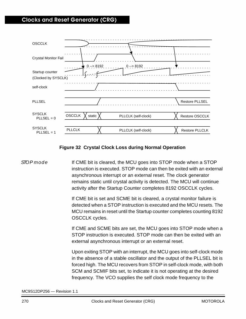
Clocks and Reset Generator (CRG)
MC9S12DP256 — Revision 1.1
270 Clocks and Reset Generator (CRG) MOTOROLA
Figure 32 Crystal Clock Loss during Normal Operation
STOP mode If CME bit is cleared, the MCU goes into STOP mode when a STOP instruction is executed. STOP mode can then be exited with an external asynchronous interrupt or an external reset. The clock generator remains static until crystal activity is detected. The MCU will continue activity after the Startup Counter completes 8192 OSCCLK cycles.
If CME bit is set and SCME bit is cleared, a crystal monitor failure is detected when a STOP instruction is executed and the MCU resets. The MCU remains in reset until the Startup counter completes counting 8192 OSCCLK cycles.
If CME and SCME bits are set, the MCU goes into STOP mode when a STOP instruction is executed. STOP mode can then be exited with an external asynchronous interrupt or an external reset.
Upon exiting STOP with an interrupt, the MCU goes into self-clock mode in the absence of a stable oscillator and the output of the PLLSEL bit is forced high. The MCU recovers from STOP in self-clock mode, with both SCM and SCMIF bits set, to indicate it is not operating at the desired frequency. The VCO supplies the self clock mode frequency to the
self-clock
PLLSEL Restore PLLSEL
SYSCLKPLLCLK (self-clock) Restore OSCCLK
OSCCLK
Crystal Monitor Fail
OSCCLK staticPLLSEL = 0
SYSCLKPLLCLK (self-clock) Restore PLLCLKPLLCLK
PLLSEL = 1
0 --> 8192
(Clocked by SYSCLK)
Startup counter
0 --> 8192
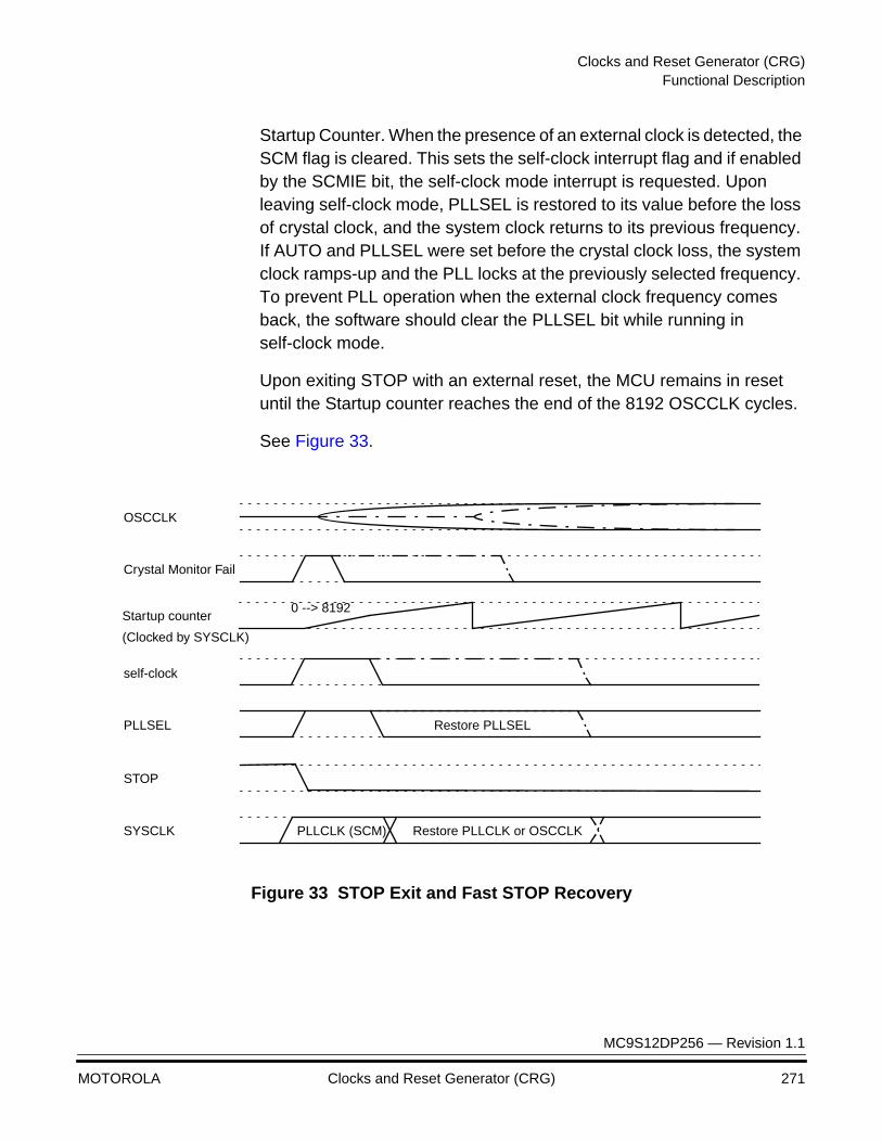
Clocks and Reset Generator (CRG)Functional Description
MC9S12DP256 — Revision 1.1
MOTOROLA Clocks and Reset Generator (CRG) 271
Startup Counter. When the presence of an external clock is detected, the SCM flag is cleared. This sets the self-clock interrupt flag and if enabled by the SCMIE bit, the self-clock mode interrupt is requested. Upon leaving self-clock mode, PLLSEL is restored to its value before the loss of crystal clock, and the system clock returns to its previous frequency. If AUTO and PLLSEL were set before the crystal clock loss, the system clock ramps-up and the PLL locks at the previously selected frequency. To prevent PLL operation when the external clock frequency comes back, the software should clear the PLLSEL bit while running in self-clock mode.
Upon exiting STOP with an external reset, the MCU remains in reset until the Startup counter reaches the end of the 8192 OSCCLK cycles.
See Figure 33.
Figure 33 STOP Exit and Fast STOP Recovery
Crystal Monitor Fail
OSCCLK
self-clock
PLLSEL Restore PLLSEL
SYSCLK PLLCLK (SCM) Restore PLLCLK or OSCCLK
STOP
Startup counter0 --> 8192
(Clocked by SYSCLK)
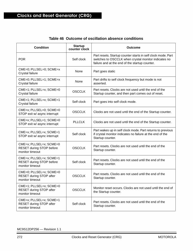
Clocks and Reset Generator (CRG)
MC9S12DP256 — Revision 1.1
272 Clocks and Reset Generator (CRG) MOTOROLA
Table 46 Outcome of oscillation absence conditions
Condition Startup counter clock Outcome
POR Self clockPart resets. Startup counter starts in self clock mode. Part switches to OSCCLK when crystal monitor indicates no failure and at the end of the startup counter.
CME=0; PLLSEL=0; SCME=xCrystal failure
None Part goes static
CME=0; PLLSEL=1; SCME=xCrystal failure
NonePart drifts to self clock frequency but mode is not asserted.
CME=1; PLLSEL=x; SCME=0Crystal failure
OSCCLKPart resets. Clocks are not used until the end of the Startup counter, and then part comes out of reset.
CME=1; PLLSEL=x; SCME=1Crystal failure
Self clock Part goes into self clock mode.
CME=x; PLLSEL=0; SCME=0STOP exit w/ async interrupt
OSCCLK Clocks are not used until the end of the Startup counter.
CME=x; PLLSEL=1; SCME=0STOP exit w/ async interrupt
PLLCLK Clocks are not used until the end of the Startup counter.
CME=x; PLLSEL=x; SCME=1STOP exit w/ async interrupt
Self clockPart wakes up in self clock mode. Part returns to previous if crystal monitor indicates no failure at the end of the Startup counter.
CME=x; PLLSEL=x; SCME=0RESET during STOP before monitor timeout
OSCCLKPart resets. Clocks are not used until the end of the Startup counter.
CME=x; PLLSEL=x; SCME=1RESET during STOP before monitor timeout
Self clockPart resets. Clocks are not used until the end of the Startup counter.
CME=0; PLLSEL=x; SCME=0RESET during STOP after monitor timeout
OSCCLKPart resets. Clocks are not used until the end of the Startup counter.
CME=1; PLLSEL=x; SCME=0RESET during STOP after monitor timeout
OSCCLKMonitor reset occurs. Clocks are not used until the end of the Startup counter.
CME=x; PLLSEL=x; SCME=1RESET during STOP after monitor timeout
Self clockPart resets. Clocks are not used until the end of the Startup counter.

Clocks and Reset Generator (CRG)Functional Description
MC9S12DP256 — Revision 1.1
MOTOROLA Clocks and Reset Generator (CRG) 273
Figure 34 Crystal loss, stop and startup sequence
MCU continuesoperation in
self clock mode
Interrupt?
Clock?
SCME=1?
Count 8192OSCCLK
Count 8192SCM Cycles
AssertSCM, SCMIF
Clocks arereleased
Wait forclock
MCU resumesnormal
operation
CPU executesSTOP instruction
Power ondetected
Clockfailure
MCU resetsCME=1
?
&SCME=0
STOP mode
YES
NO NO
NO
YES
NO
YES
NO
Clock?
YES
YES
NO
Clock?
YES
NO
Count 8192SCM cycles
Clock?
YES
NO
Deassert SCMClocks resume
normaloperation
MCU resetsCME=1
?
&SCME=0
YES
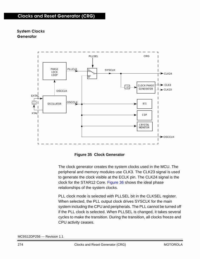
Clocks and Reset Generator (CRG)
MC9S12DP256 — Revision 1.1
274 Clocks and Reset Generator (CRG) MOTOROLA
System Clocks Generator
Figure 35 Clock Generator
The clock generator creates the system clocks used in the MCU. The peripheral and memory modules use CLK3. The CLK23 signal is used to generate the clock visible at the ECLK pin. The CLK24 signal is the clock for the STAR12 Core. Figure 36 shows the ideal phase relationships of the system clocks.
PLL clock mode is selected with PLLSEL bit in the CLKSEL register. When selected, the PLL output clock drives SYSCLK for the main system including the CPU and peripherals. The PLL cannot be turned off if the PLL clock is selected. When PLLSEL is changed, it takes several cycles to make the transition. During the transition, all clocks freeze and CPU activity ceases.
OSCILLATOR
PHASELOCKLOOP
EXTAL
XTAL
SYSCLK
RTIOSCCLK
OSCCLK
PLLCLK
CLOCK PHASEGENERATOR CLK23
CLK3
CRYSTAL MONITOR
1
0
PLLSEL
÷2
CLK24
COP
OSCCLK
CRG
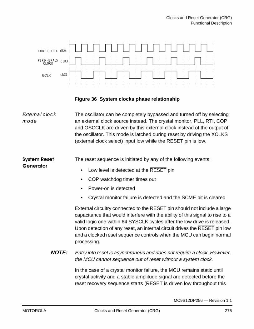
Clocks and Reset Generator (CRG)Functional Description
MC9S12DP256 — Revision 1.1
MOTOROLA Clocks and Reset Generator (CRG) 275
Figure 36 System clocks phase relationship
External clock mode
The oscillator can be completely bypassed and turned off by selecting an external clock source instead. The crystal monitor, PLL, RTI, COP and OSCCLK are driven by this external clock instead of the output of the oscillator. This mode is latched during reset by driving the XCLKS (external clock select) input low while the RESET pin is low.
System Reset Generator
The reset sequence is initiated by any of the following events:
• Low level is detected at the RESET pin
• COP watchdog timer times out
• Power-on is detected
• Crystal monitor failure is detected and the SCME bit is cleared
External circuitry connected to the RESET pin should not include a large capacitance that would interfere with the ability of this signal to rise to a valid logic one within 64 SYSCLK cycles after the low drive is released. Upon detection of any reset, an internal circuit drives the RESET pin low and a clocked reset sequence controls when the MCU can begin normal processing.
NOTE: Entry into reset is asynchronous and does not require a clock. However, the MCU cannot sequence out of reset without a system clock.
In the case of a crystal monitor failure, the MCU remains static until crystal activity and a stable amplitude signal are detected before the reset recovery sequence starts (RESET is driven low throughout this
CORE CLOCK
CLK3
clk23
PERIPHERALSCLOCK
clk24
ECLK

Clocks and Reset Generator (CRG)
MC9S12DP256 — Revision 1.1
276 Clocks and Reset Generator (CRG) MOTOROLA
static period). In the case of POR, the reset recovery sequence starts in self clock mode. The internal reset recovery sequence then drives RESET low for 128 SYSCLK cycles and releases the drive to allow RESET to rise. 64 SYSCLK cycles later this circuit samples the RESET pin to see if it has risen to a logic one level. If RESET is low at this point, the reset is assumed to be coming from an external request and the internally latched states of the COP timeout and crystal monitor failure are cleared so the normal reset vector ($FFFE:FFFF) is taken when RESET is finally released. If RESET is high after this 64 cycle delay, the reset source is tentatively assumed to be either a COP failure or a crystal monitor failure. If the internally latched state of the crystal monitor fail circuit is true, processing begins by fetching the crystal monitor vector ($FFFC:FFFD). If no crystal monitor failure is indicated, and the latched state of the COP timeout is true, processing begins by fetching the COP vector ($FFFA:FFFB). If neither crystal monitor fail nor COP timeout are pending, processing begins by fetching the normal reset vector ($FFFE:FFFF).
Computer Operating Properly (COP) Watchdog
The COP watchdog enables the user to check that a program is running and sequencing properly. When the COP is being used, software is responsible for keeping a free running watchdog timer from timing out. If the watchdog timer times out it is an indication that the software is no longer being executed in the intended sequence; thus a system reset is initiated. The watchdog timer runs with OSCCLK. Three control bits in the COPCTL register allow selection of seven COP time-out periods.
When COP is enabled, the program must write $55 and $AA (in this order) to the ARMCOP register during the selected time-out period. Once this is done, the internal COP counter resets to the start of a new time-out period. If the program fails to do this the part will reset. Also, if any value other than $55 or $AA is written, the part is immediately reset.
Windowed COP operation is enabled by setting WCOP in the COPCTL register. In this mode, writes to the ARMCOP register to clear the COP timer must occur in the last 25% of the selected time-out period. A premature write will immediately reset the part. See Figure 37.
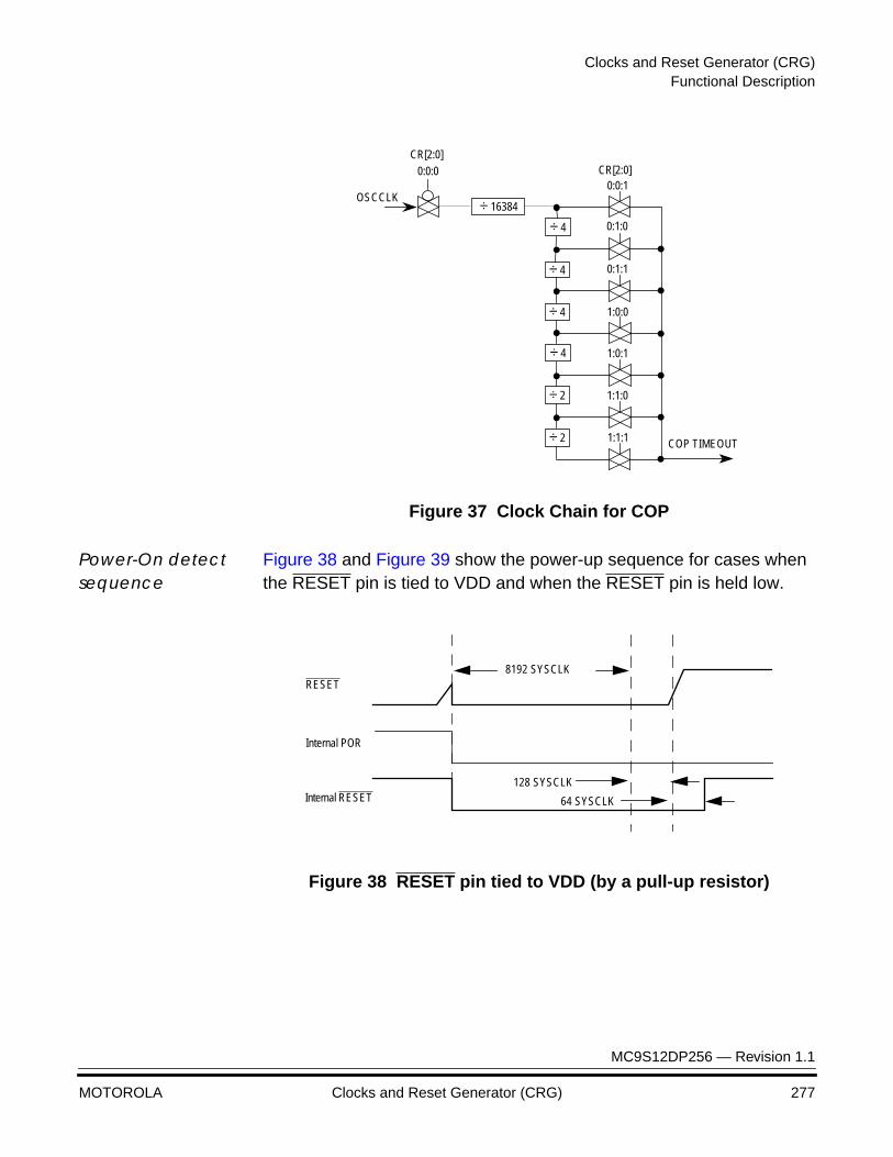
Clocks and Reset Generator (CRG)Functional Description
MC9S12DP256 — Revision 1.1
MOTOROLA Clocks and Reset Generator (CRG) 277
Figure 37 Clock Chain for COP
Power-On detect sequence
Figure 38 and Figure 39 show the power-up sequence for cases when the RESET pin is tied to VDD and when the RESET pin is held low.
Figure 38 RESET pin tied to VDD (by a pull-up resistor)
OSCCLK
CR[2:0]
COP TIMEOUT
0:0:00:0:1
0:1:0
0:1:1
1:0:0
1:0:1
1:1:0
1:1:1
÷ 4
÷ 4
÷ 2
÷ 4
÷ 2
÷ 16384
÷ 4
CR[2:0]
RESET
Internal POR
128 SYSCLK
64 SYSCLKInternal RESET
8192 SYSCLK
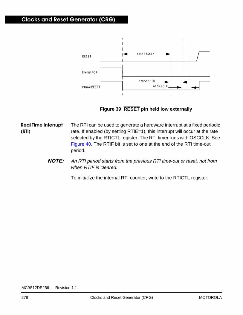
Clocks and Reset Generator (CRG)
MC9S12DP256 — Revision 1.1
278 Clocks and Reset Generator (CRG) MOTOROLA
Figure 39 RESET pin held low externally
Real Time Interrupt (RTI)
The RTI can be used to generate a hardware interrupt at a fixed periodic rate. If enabled (by setting RTIE=1), this interrupt will occur at the rate selected by the RTICTL register. The RTI timer runs with OSCCLK. See Figure 40. The RTIF bit is set to one at the end of the RTI time-out period.
NOTE: An RTI period starts from the previous RTI time-out or reset, not from when RTIF is cleared.
To initialize the internal RTI counter, write to the RTICTL register.
8192 SYSCLKRESET
Internal POR
Internal RESET
128 SYSCLK
64 SYSCLK
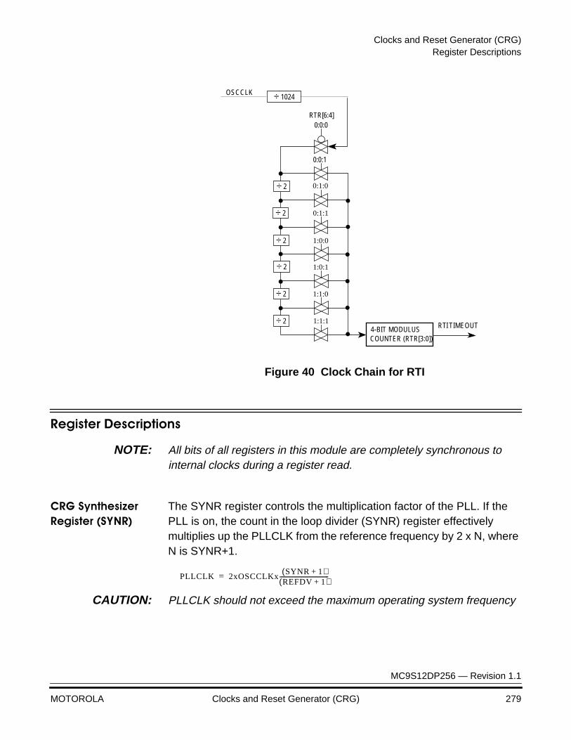
Clocks and Reset Generator (CRG)Register Descriptions
MC9S12DP256 — Revision 1.1
MOTOROLA Clocks and Reset Generator (CRG) 279
Figure 40 Clock Chain for RTI
Register Descriptions
NOTE: All bits of all registers in this module are completely synchronous to internal clocks during a register read.
CRG Synthesizer Register (SYNR)
The SYNR register controls the multiplication factor of the PLL. If the PLL is on, the count in the loop divider (SYNR) register effectively multiplies up the PLLCLK from the reference frequency by 2 x N, where N is SYNR+1.
CAUTION: PLLCLK should not exceed the maximum operating system frequency
OSCCLK
RTR[6:4]0:0:0
0:0:1
0:1:0
0:1:1
1:0:0
1:0:1
1:1:0
1:1:1
÷ 2
÷ 2
÷ 2
÷ 2
÷ 2
÷ 2
COUNTER (RTR[3:0])4-BIT MODULUS
÷ 1024
RTI TIMEOUT
PLLCLK 2xOSCCLKxSYNR 1+( )
REFDV 1+( )-----------------------------------=
Clocks and Reset Generator (CRG)
MC9S12DP256 — Revision 1.1
280 Clocks and Reset Generator (CRG) MOTOROLA
.
Read: anytime.
Write: anytime except if PLLSEL = 1.
Write to this register initializes the lock detector.
CRG Reference Divider Register (REFDV)
The REFDV register provides a finer granularity for the PLL multiplier steps. The count in the reference divider divides OSCCLK frequency by REFDV+1.
Read: anytime.
Write: anytime except when PLLSEL = 1.
Write to this register initializes the lock detector.
Address Offset: $0000
Bit 7 6 5 4 3 2 1 0
Read: 0 0SYN5 SYN4 SYN3 SYN2 SYN1 SYN0
Write:
Reset: 0 0 0 0 0 0 0 0
= Unimplemented or reserved
Address Offset: $0001
Bit 7 6 5 4 3 2 1 0
Read: 0 0 0 0REFDV3 REFDV2 REFDV1 REFDV0
Write:
Reset: 0 0 0 0 0 0 0 0
= Unimplemented or reserved
Clocks and Reset Generator (CRG)Register Descriptions
MC9S12DP256 — Revision 1.1
MOTOROLA Clocks and Reset Generator (CRG) 281
CRG Test Flags Register (CTFLG)
The CTFLG register is reserved for test mode only.:
Read: always read $00 except in test modes.
Write: only in test modes.
CRG Flags Register (CRGFLG)
Read anytime. Refer to each bit for write conditions.
RTIF — Real Time Interrupt Flag
The RTIF bit is automatically set to one at the end of every RTI period. This flag can only be cleared by writing a 1. Writing a 0 has no effect.
0 = Time-out has not yet occurred.1 = Set when the time-out period is met.
PORF — Power on Reset Flag
The PORF bit is automatically set to one when a power on reset occurs. This flag can only be cleared by writing a 1. Writing a 0 has no effect.
0 = Power on reset has not yet occurred
Address Offset: $0002
Bit 7 6 5 4 3 2 1 0
Read:TOUT7 TOUT6 TOUT5 TOUT4 TOUT3 TOUT2 TOUT1 TOUT0
Write:
Reset: 0 0 0 0 0 0 0 0
Address Offset: $0003
Bit 7 6 5 4 3 2 1 0
Read:RTIF PORF
0LOCKIF
LOCK TRACKSCMIF
SCM
Write:
Reset: 0 (1) 0 0 0 0 0 0
= Unimplemented or reserved
1. PORF set to 1 when a power on reset occurs. Unaffected by non-POR resets.

Clocks and Reset Generator (CRG)
MC9S12DP256 — Revision 1.1
282 Clocks and Reset Generator (CRG) MOTOROLA
1 = Set when a power on reset has occurred
LOCKIF — PLL Lock Interrupt Flag
This flag can only be cleared by writing a 1. Writing a 0 has no effect.0 = No change in LOCK bit1 = LOCK condition has changed, either from a locked state to an
unlocked state or vice versa.
LOCK — Lock Status
Write never. This bit is cleared in Self-Clocked Mode as the lock detector can not operate without the reference frequency.
0 = PLL VCO is not within the desired tolerance of the target frequency.
1 = After the PLL is turned on, indicates the PLL VCO is within the desired tolerance of the target frequency.
TRACK — Track Status
Write never. This bit is cleared in Self-Clocked Mode as the lock detector can not operate without the reference frequency. See Acquisition and tracking Modes for more information.
0 = Acquisition mode status.1 = Tracking mode status.
SCMIF — Self-clock mode Interrupt Flag
The flag can only be cleared by writing a 1. Writing a 0 has no effect. 0 = No change in SCM bit.1 = SCM condition has changed, either entered or exited self-clock
mode.
SCM — Self-clock mode Status
Write never. See Crystal loss, stop and startup for more information.0 = MCU is operating normally with OSCCLK available.1 = PLL self-clock is supplied to the MCU upon loss of OSCCLK.
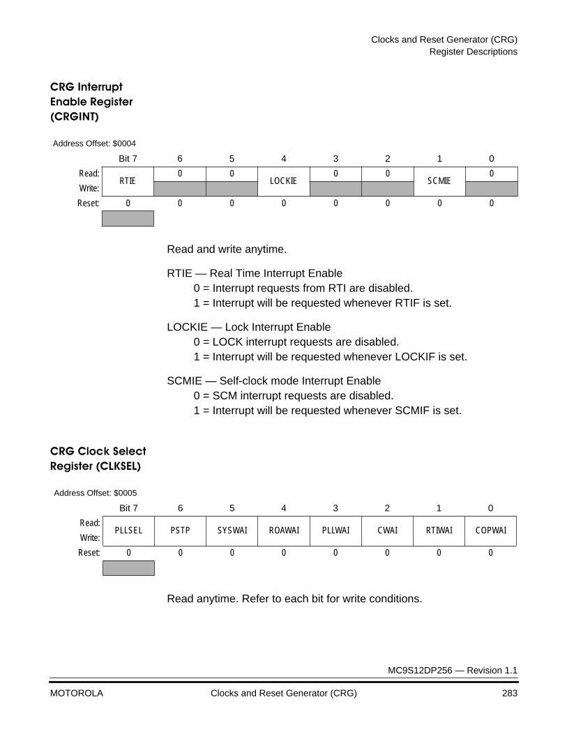
Clocks and Reset Generator (CRG)Register Descriptions
MC9S12DP256 — Revision 1.1
MOTOROLA Clocks and Reset Generator (CRG) 283
CRG Interrupt Enable Register (CRGINT)
Read and write anytime.
RTIE — Real Time Interrupt Enable0 = Interrupt requests from RTI are disabled.1 = Interrupt will be requested whenever RTIF is set.
LOCKIE — Lock Interrupt Enable0 = LOCK interrupt requests are disabled.1 = Interrupt will be requested whenever LOCKIF is set.
SCMIE — Self-clock mode Interrupt Enable0 = SCM interrupt requests are disabled.1 = Interrupt will be requested whenever SCMIF is set.
CRG Clock Select Register (CLKSEL)
Read anytime. Refer to each bit for write conditions.
Address Offset: $0004
Bit 7 6 5 4 3 2 1 0
Read:RTIE
0 0LOCKIE
0 0SCMIE
0
Write:
Reset: 0 0 0 0 0 0 0 0
Address Offset: $0005
Bit 7 6 5 4 3 2 1 0
Read:PLLSEL PSTP SYSWAI ROAWAI PLLWAI CWAI RTIWAI COPWAI
Write:
Reset: 0 0 0 0 0 0 0 0
Clocks and Reset Generator (CRG)
MC9S12DP256 — Revision 1.1
284 Clocks and Reset Generator (CRG) MOTOROLA
PLLSEL — PLL selected for system clock
Write anytime except when LOCK is cleared and AUTO is set, or TRACK is cleared and AUTO is cleared. In self-clock mode, the output of the PLLSEL bit is forced to 1, but the PLLSEL bit reads the latched value.
0 = SYSCLK is derived from OSCCLK.1 = SYSCLK is derived from PLLCLK.
PSTP — Pseudo Stop
User mode: Write once
Test mode: Write anytime
In Pseudo-STOP mode, the oscillator is still running while the MCU is maintained in STOP mode.
0 = Pseudo-STOP oscillator mode is disabled.1 = Pseudo-STOP oscillator mode is enabled.
NOTE: Pseudo-STOP allows for faster STOP recovery and reduces the mechanical stress and aging of the resonator in case of frequent STOP conditions at the expense of a slightly increased power consumption.
SYSWAI — System clocks stop in WAIT mode
User mode: Write once
Test mode: Write anytime0 = Allows the system clocks to continue running in wait mode.1 = Disables all the system clocks (CLK24, CLK23, CLK3 and
OSCCLK) whenever the part goes into wait mode.
NOTE: RTI and COP are not affected by SYSWAI bit.
ROAWAI — Reduced Oscillator Amplitude in WAIT mode
User mode: Write once
Test mode: Write anytime0 = Normal peak-peak oscillator amplitude in wait mode.1 = Reduced peak-peak oscillator amplitude in wait mode.
NOTE: Lower peak to peak oscillator amplitude exhibit lower power consumption but could have adverse effects during any Electro-Magnetic Susceptibility (EMS) tests.
Clocks and Reset Generator (CRG)Register Descriptions
MC9S12DP256 — Revision 1.1
MOTOROLA Clocks and Reset Generator (CRG) 285
PLLWAI — PLL stops in WAIT mode
User mode: Write once
Test mode: Write anytime
If PLLWAI is set, PLLON and PLLSEL bits remain set during wait mode but the PLL is powered down. Upon exiting wait mode, an automatic recovery delay is imposed until LOCK is detected. AUTO bit is forced to 1 if PLLWAI is set.
0 = Allows the PLL to keep running in wait mode.1 = Disables the PLL whenever the part goes into wait mode.
CWAI — CLK24 and CLK23 stop in WAIT mode
User mode: Write once
Test mode: Write anytime0 = Allows CLK24 and CLK23 to continue running in wait mode.1 = Disables CLK24 and CLK23 whenever the part goes into wait
mode.
RTIWAI — RTI stops in WAIT mode
User mode: Write once
Test mode: Write anytime0 = Allows the RTI to continue running in wait mode.1 = Disables and initializes the RTI dividers whenever the part goes
into wait mode.
COPWAI — COP stops in WAIT mode
User mode: Write once
Test mode: Write anytime0 = Allows the COP to continue running in wait mode.1 = Disables and initializes the COP dividers whenever the part
goes into wait mode.
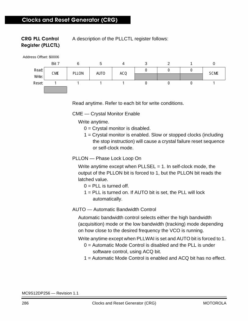
Clocks and Reset Generator (CRG)
MC9S12DP256 — Revision 1.1
286 Clocks and Reset Generator (CRG) MOTOROLA
CRG PLL Control Register (PLLCTL)
A description of the PLLCTL register follows:
Read anytime. Refer to each bit for write conditions.
CME — Crystal Monitor Enable
Write anytime.0 = Crystal monitor is disabled.1 = Crystal monitor is enabled. Slow or stopped clocks (including
the stop instruction) will cause a crystal failure reset sequence or self-clock mode.
PLLON — Phase Lock Loop On
Write anytime except when PLLSEL = 1. In self-clock mode, the output of the PLLON bit is forced to 1, but the PLLON bit reads the latched value.
0 = PLL is turned off.1 = PLL is turned on. If AUTO bit is set, the PLL will lock
automatically.
AUTO — Automatic Bandwidth Control
Automatic bandwidth control selects either the high bandwidth (acquisition) mode or the low bandwidth (tracking) mode depending on how close to the desired frequency the VCO is running.
Write anytime except when PLLWAI is set and AUTO bit is forced to 1.0 = Automatic Mode Control is disabled and the PLL is under
software control, using ACQ bit.1 = Automatic Mode Control is enabled and ACQ bit has no effect.
Address Offset: $0006
Bit 7 6 5 4 3 2 1 0
Read:CME PLLON AUTO ACQ
0 0 0SCME
Write:
Reset: 1 1 1 1 0 0 0 1
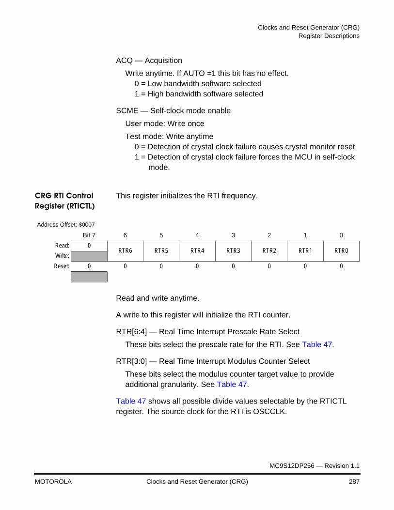
Clocks and Reset Generator (CRG)Register Descriptions
MC9S12DP256 — Revision 1.1
MOTOROLA Clocks and Reset Generator (CRG) 287
ACQ — Acquisition
Write anytime. If AUTO =1 this bit has no effect.0 = Low bandwidth software selected1 = High bandwidth software selected
SCME — Self-clock mode enable
User mode: Write once
Test mode: Write anytime0 = Detection of crystal clock failure causes crystal monitor reset1 = Detection of crystal clock failure forces the MCU in self-clock
mode.
CRG RTI Control Register (RTICTL)
This register initializes the RTI frequency.
Read and write anytime.
A write to this register will initialize the RTI counter.
RTR[6:4] — Real Time Interrupt Prescale Rate Select
These bits select the prescale rate for the RTI. See Table 47.
RTR[3:0] — Real Time Interrupt Modulus Counter Select
These bits select the modulus counter target value to provide additional granularity. See Table 47.
Table 47 shows all possible divide values selectable by the RTICTL register. The source clock for the RTI is OSCCLK.
Address Offset: $0007
Bit 7 6 5 4 3 2 1 0
Read: 0RTR6 RTR5 RTR4 RTR3 RTR2 RTR1 RTR0
Write:
Reset: 0 0 0 0 0 0 0 0
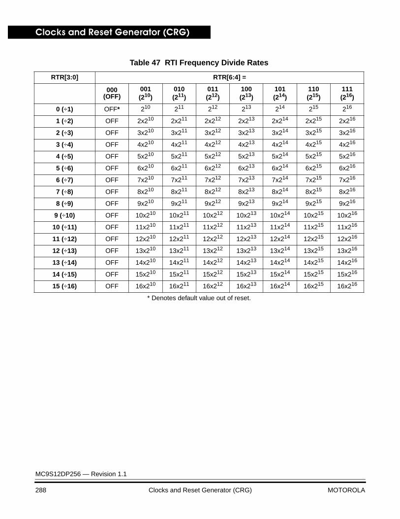
Clocks and Reset Generator (CRG)
MC9S12DP256 — Revision 1.1
288 Clocks and Reset Generator (CRG) MOTOROLA
Table 47 RTI Frequency Divide Rates
RTR[3:0] RTR[6:4] =
000(OFF)
001(210)
010(211)
011(212)
100(213)
101(214)
110(215)
111(216)
0 (÷1) OFF* 210 211 212 213 214 215 216
1 (÷2) OFF 2x210 2x211 2x212 2x213 2x214 2x215 2x216
2 (÷3) OFF 3x210 3x211 3x212 3x213 3x214 3x215 3x216
3 (÷4) OFF 4x210 4x211 4x212 4x213 4x214 4x215 4x216
4 (÷5) OFF 5x210 5x211 5x212 5x213 5x214 5x215 5x216
5 (÷6) OFF 6x210 6x211 6x212 6x213 6x214 6x215 6x216
6 (÷7) OFF 7x210 7x211 7x212 7x213 7x214 7x215 7x216
7 (÷8) OFF 8x210 8x211 8x212 8x213 8x214 8x215 8x216
8 (÷9) OFF 9x210 9x211 9x212 9x213 9x214 9x215 9x216
9 (÷10) OFF 10x210 10x211 10x212 10x213 10x214 10x215 10x216
10 (÷11) OFF 11x210 11x211 11x212 11x213 11x214 11x215 11x216
11 (÷12) OFF 12x210 12x211 12x212 12x213 12x214 12x215 12x216
12 (÷13) OFF 13x210 13x211 13x212 13x213 13x214 13x215 13x216
13 (÷14) OFF 14x210 14x211 14x212 14x213 14x214 14x215 14x216
14 (÷15) OFF 15x210 15x211 15x212 15x213 15x214 15x215 15x216
15 (÷16) OFF 16x210 16x211 16x212 16x213 16x214 16x215 16x216
* Denotes default value out of reset.
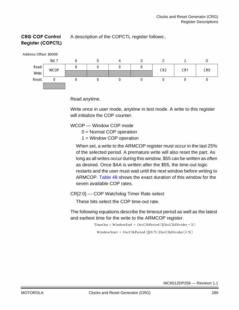
Clocks and Reset Generator (CRG)Register Descriptions
MC9S12DP256 — Revision 1.1
MOTOROLA Clocks and Reset Generator (CRG) 289
CRG COP Control Register (COPCTL)
A description of the COPCTL register follows:.
Read anytime.
Write once in user mode, anytime in test mode. A write to this register will initialize the COP counter.
WCOP — Window COP mode0 = Normal COP operation1 = Window COP operation
When set, a write to the ARMCOP register must occur in the last 25% of the selected period. A premature write will also reset the part. As long as all writes occur during this window, $55 can be written as often as desired. Once $AA is written after the $55, the time-out logic restarts and the user must wait until the next window before writing to ARMCOP. Table 48 shows the exact duration of this window for the seven available COP rates.
CR[2:0] — COP Watchdog Timer Rate select
These bits select the COP time-out rate.
The following equations describe the timeout period as well as the latest and earliest time for the write to the ARMCOP register.
Address Offset: $0008
Bit 7 6 5 4 3 2 1 0
Read:WCOP
0 0 0 0CR2 CR1 CR0
Write:
Reset: 0 0 0 0 0 0 0 0
TimeOut WindowEnd= OscClkPeriod OscClkDivider 3+( )⋅=
WindowStart OscClkPeriod 0.75 OscClkDivider⋅( ) 9+( )⋅=
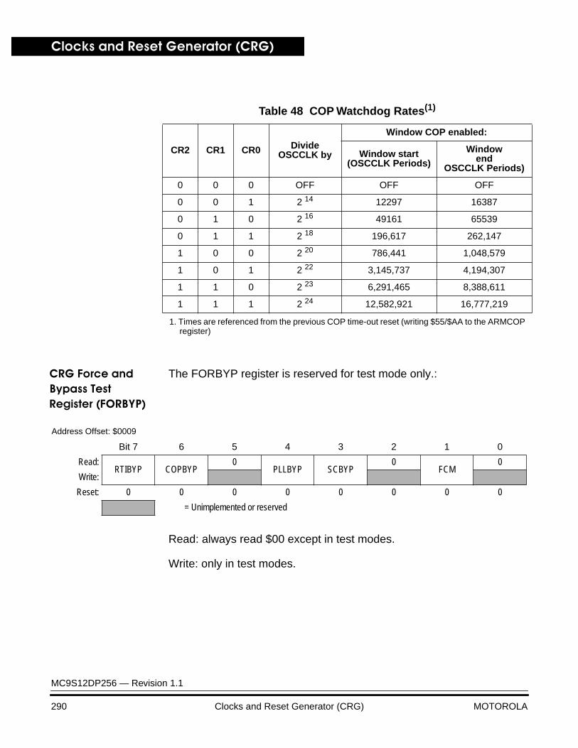
Clocks and Reset Generator (CRG)
MC9S12DP256 — Revision 1.1
290 Clocks and Reset Generator (CRG) MOTOROLA
CRG Force and Bypass Test Register (FORBYP)
The FORBYP register is reserved for test mode only.:
Read: always read $00 except in test modes.
Write: only in test modes.
Table 48 COP Watchdog Rates(1)
1. Times are referenced from the previous COP time-out reset (writing $55/$AA to the ARMCOPregister)
CR2 CR1 CR0 Divide OSCCLK by
Window COP enabled:
Window start(OSCCLK Periods)
Windowend
OSCCLK Periods)
0 0 0 OFF OFF OFF
0 0 1 2 14 12297 16387
0 1 0 2 16 49161 65539
0 1 1 2 18 196,617 262,147
1 0 0 2 20 786,441 1,048,579
1 0 1 2 22 3,145,737 4,194,307
1 1 0 2 23 6,291,465 8,388,611
1 1 1 2 24 12,582,921 16,777,219
Address Offset: $0009
Bit 7 6 5 4 3 2 1 0
Read:RTIBYP COPBYP
0PLLBYP SCBYP
0FCM
0
Write:
Reset: 0 0 0 0 0 0 0 0
= Unimplemented or reserved
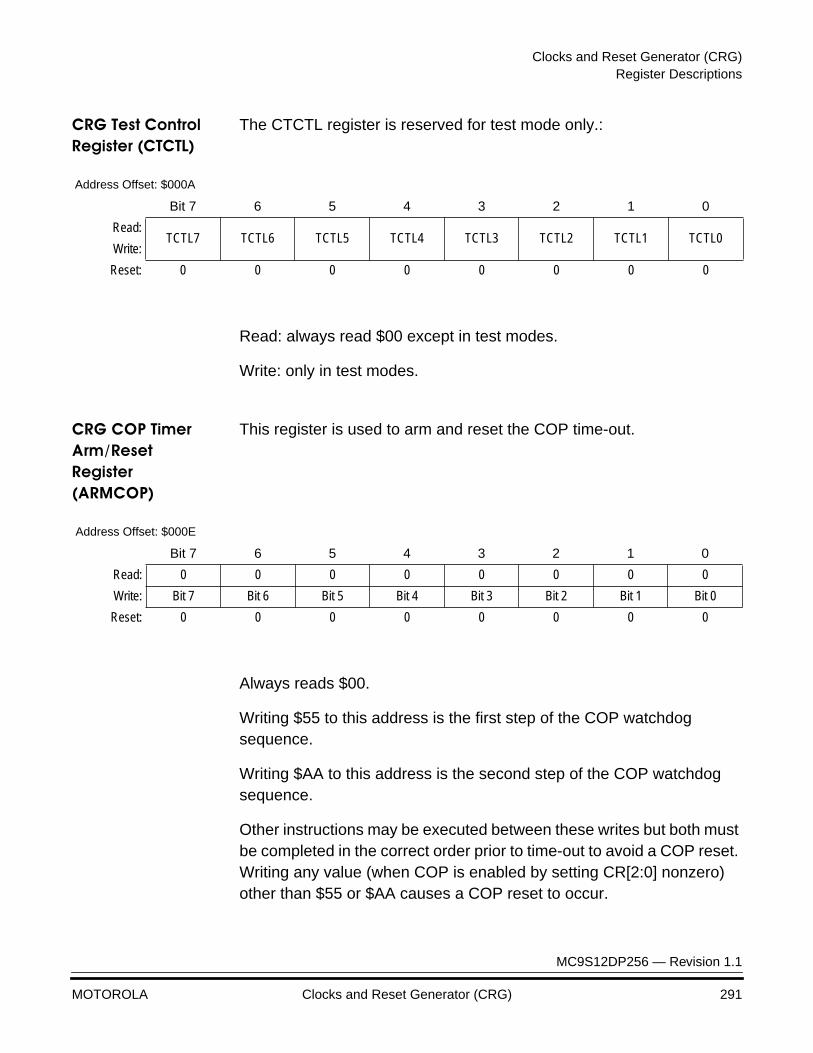
Clocks and Reset Generator (CRG)Register Descriptions
MC9S12DP256 — Revision 1.1
MOTOROLA Clocks and Reset Generator (CRG) 291
CRG Test Control Register (CTCTL)
The CTCTL register is reserved for test mode only.:
Read: always read $00 except in test modes.
Write: only in test modes.
CRG COP Timer Arm/Reset Register (ARMCOP)
This register is used to arm and reset the COP time-out.
Always reads $00.
Writing $55 to this address is the first step of the COP watchdog sequence.
Writing $AA to this address is the second step of the COP watchdog sequence.
Other instructions may be executed between these writes but both must be completed in the correct order prior to time-out to avoid a COP reset. Writing any value (when COP is enabled by setting CR[2:0] nonzero) other than $55 or $AA causes a COP reset to occur.
Address Offset: $000A
Bit 7 6 5 4 3 2 1 0
Read:TCTL7 TCTL6 TCTL5 TCTL4 TCTL3 TCTL2 TCTL1 TCTL0
Write:
Reset: 0 0 0 0 0 0 0 0
Address Offset: $000E
Bit 7 6 5 4 3 2 1 0
Read: 0 0 0 0 0 0 0 0
Write: Bit 7 Bit 6 Bit 5 Bit 4 Bit 3 Bit 2 Bit 1 Bit 0
Reset: 0 0 0 0 0 0 0 0
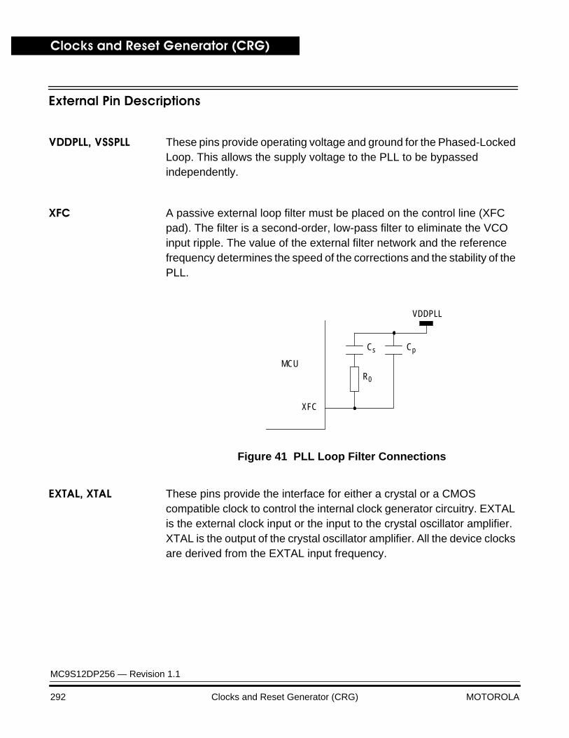
Clocks and Reset Generator (CRG)
MC9S12DP256 — Revision 1.1
292 Clocks and Reset Generator (CRG) MOTOROLA
External Pin Descriptions
VDDPLL, VSSPLL These pins provide operating voltage and ground for the Phased-Locked Loop. This allows the supply voltage to the PLL to be bypassed independently.
XFC A passive external loop filter must be placed on the control line (XFC pad). The filter is a second-order, low-pass filter to eliminate the VCO input ripple. The value of the external filter network and the reference frequency determines the speed of the corrections and the stability of the PLL.
Figure 41 PLL Loop Filter Connections
EXTAL, XTAL These pins provide the interface for either a crystal or a CMOS compatible clock to control the internal clock generator circuitry. EXTAL is the external clock input or the input to the crystal oscillator amplifier. XTAL is the output of the crystal oscillator amplifier. All the device clocks are derived from the EXTAL input frequency.
MCU
XFC
R0
Cs
VDDPLL
Cp
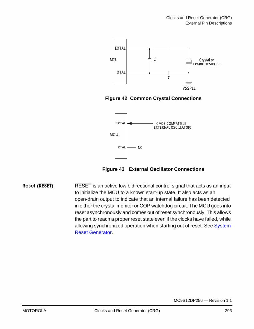
Clocks and Reset Generator (CRG)External Pin Descriptions
MC9S12DP256 — Revision 1.1
MOTOROLA Clocks and Reset Generator (CRG) 293
Figure 42 Common Crystal Connections
Figure 43 External Oscillator Connections
Reset (RESET) RESET is an active low bidirectional control signal that acts as an input to initialize the MCU to a known start-up state. It also acts as an open-drain output to indicate that an internal failure has been detected in either the crystal monitor or COP watchdog circuit. The MCU goes into reset asynchronously and comes out of reset synchronously. This allows the part to reach a proper reset state even if the clocks have failed, while allowing synchronized operation when starting out of reset. See System Reset Generator.
MCU
C
EXTAL
XTAL
Crystal or
VSSPLL
ceramic resonatorC
MCU
EXTAL
XTAL
CMOS-COMPATIBLEEXTERNAL OSCILLATOR
NC

Clocks and Reset Generator (CRG)
MC9S12DP256 — Revision 1.1
294 Clocks and Reset Generator (CRG) MOTOROLA
Reset Initialization
When a reset occurs, CRG registers and control bits are changed to known start-up states, as outlined in Register Descriptions.
Interrupt Operation
Real Time Interrupt The CRG generates a real time interrupt when the selected interrupt time period elapses. RTI interrupts are locally disabled by setting the RTIE bit to zero. The real time interrupt flag (RTIF) is set to1 when a timeout occurs, and is cleared to 0 by a write to 1 to the RTIF bit.
COP (Computer Operating Properly) Watchdog Reset
The device will generate a reset when a COP watchdog failure occurs. This is locally disabled by setting the COP rate select bits in COPCTL (CR2,CR1,CR0) to zero.
Crystal Monitor Reset
The device will generate a reset when a crystal monitor failure occurs. This is locally disabled by clearing CME bit in PLLCTL register.
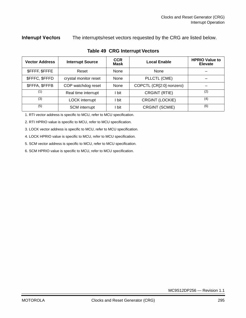
Clocks and Reset Generator (CRG)Interrupt Operation
MC9S12DP256 — Revision 1.1
MOTOROLA Clocks and Reset Generator (CRG) 295
Interrupt Vectors The interrupts/reset vectors requested by the CRG are listed below.
Table 49 CRG Interrupt Vectors
Vector Address Interrupt Source CCR Mask Local Enable HPRIO Value to
Elevate
$FFFF, $FFFE Reset None None –
$FFFC, $FFFD crystal monitor reset None PLLCTL (CME) –
$FFFA, $FFFB COP watchdog reset None COPCTL (CR[2:0] nonzero) –(1) Real time interrupt I bit CRGINT (RTIE) (2)
(3) LOCK interrupt I bit CRGINT (LOCKIE) (4)
(5) SCM interrupt I bit CRGINT (SCMIE) (6)
1. RTI vector address is specific to MCU, refer to MCU specification.
2. RTI HPRIO value is specific to MCU, refer to MCU specification.
3. LOCK vector address is specific to MCU, refer to MCU specification.
4. LOCK HPRIO value is specific to MCU, refer to MCU specification.
5. SCM vector address is specific to MCU, refer to MCU specification.
6. SCM HPRIO value is specific to MCU, refer to MCU specification.
Clocks and Reset Generator (CRG)
MC9S12DP256 — Revision 1.1
296 Clocks and Reset Generator (CRG) MOTOROLA
Low Power Options
This section summarizes the low power options available in the CRG sub-block. Low power design practices are implemented where possible.
Run Mode The RTI can be stopped by setting the associated rate select bits to zero. The COP can be stopped by setting the associated rate select bits to zero in special mode.
Wait Mode During WAIT mode if SYSWAI bit is set, CLK24, CLK3, CLK23 and OSCCLK to peripherals are not running.
During WAIT mode if CWAI bit is set, CLK24and CLK23 are not running.
The RTI stays running during WAIT mode unless RTIWAI is set. If the RTIWAI bit is set the RTI dividers get initialized during WAIT mode.
The COP stays running during WAIT mode unless COPWAI is set. If the COPWAI bit is set, the COP dividers get initialized during WAIT mode.
The Crystal Monitor stays running during WAIT mode unless CME is cleared.
The PLL shuts down during WAIT mode and recovers automatically if PLLWAI bit is set.
Stop Mode All clocks are stopped in STOP mode. The oscillator is disabled in STOP mode unless the PSTP bit is set. All counters and dividers remain frozen but do not initialize.

MC9S12DP256 — Revision 1.1
MOTOROLA Pulse Width Modulator (PWM) 297
Pulse Width Modulator (PWM)Pulse Width Modulator (PWM)
Contents
Overview . . . . . . . . . . . . . . . . . . . . . . . . . . . . . . . . . . . . . . . . . . . . . . 297Features . . . . . . . . . . . . . . . . . . . . . . . . . . . . . . . . . . . . . . . . . . . . . . 298Block Diagram. . . . . . . . . . . . . . . . . . . . . . . . . . . . . . . . . . . . . . . . . . 299External Pin Descriptions . . . . . . . . . . . . . . . . . . . . . . . . . . . . . . . . . 299Register Map. . . . . . . . . . . . . . . . . . . . . . . . . . . . . . . . . . . . . . . . . . . 300Register Descriptions . . . . . . . . . . . . . . . . . . . . . . . . . . . . . . . . . . . . 302Functional Description. . . . . . . . . . . . . . . . . . . . . . . . . . . . . . . . . . . . 324Reset Initialization . . . . . . . . . . . . . . . . . . . . . . . . . . . . . . . . . . . . . . . 338Modes of Operation. . . . . . . . . . . . . . . . . . . . . . . . . . . . . . . . . . . . . . 339Low Power Options . . . . . . . . . . . . . . . . . . . . . . . . . . . . . . . . . . . . . . 340Interrupt Operation . . . . . . . . . . . . . . . . . . . . . . . . . . . . . . . . . . . . . . 340
Overview
The Pulse Width Modulation (PWM) definition is based on the MC68HC11KD2 and the HC12 PWM definitions. This PWM contains the basic features from the HC11 with some of the enhancements incorporated on the HC12. In addition, the module is now expanded to eight channels with independent control of left and center aligned outputs on each channel. In all basic functionality, it will behave similarly to the HC11 PWM with the additional HC12 PWM features of center aligned output mode and four available clock sources.
The PWM module contains eight channels. Each of these channels has a programmable period and duty cycle as well as a dedicated counter. A flexible clock select scheme allows a total of four different clock sources to be used with the counters. Each of the modulators can create independent continuous waveforms with software-selectable duty rates
Pulse Width Modulator (PWM)
MC9S12DP256 — Revision 1.1
298 Pulse Width Modulator (PWM) MOTOROLA
from 0% to 100%. The PWM outputs can be programmed as left aligned outputs or center aligned outputs.
Features
• Eight independent PWM channels with programmable period and duty cycle.
• Dedicated counter for each PWM channel.
• Programmable PWM enable/disable for each channel.
• Software selection of PWM duty pulse polarity for each channel.
• Period and duty cycle are double buffered. Change takes effect when the end of the effective period is reached (PWM counter reaches zero) or when the channel is disabled.
• Programmable center or left aligned outputs on individual channels.
• Eight 8-bit channel or four 16-bit channel PWM resolution.
• Four clock sources (A, B, SA and SB) provide for a wide range of frequencies.
• Programmable Clock Select Logic.
• Emergency shutdown.
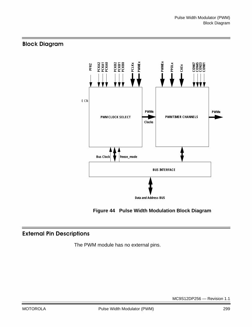
Pulse Width Modulator (PWM)Block Diagram
MC9S12DP256 — Revision 1.1
MOTOROLA Pulse Width Modulator (PWM) 299
Block Diagram
Figure 44 Pulse Width Modulation Block Diagram
External Pin Descriptions
The PWM module has no external pins.
E Clk
PWM CLOCK SELECT PWM TIMER CHANNELS
BUS INTERFACE
PFR
Z
PCK
A2
PCK
A0
PCK
A1
PCK
B2
PCK
B0
PCK
B1
PCLK
x
PWMx
Clocks
CO
N67
CO
N23
CO
N45
CO
N01
PWMx
CA
Ex
PW
ME
x
PPO
Lx
PW
ME
x
Bus Clock freeze_mode
Data and Address BUS
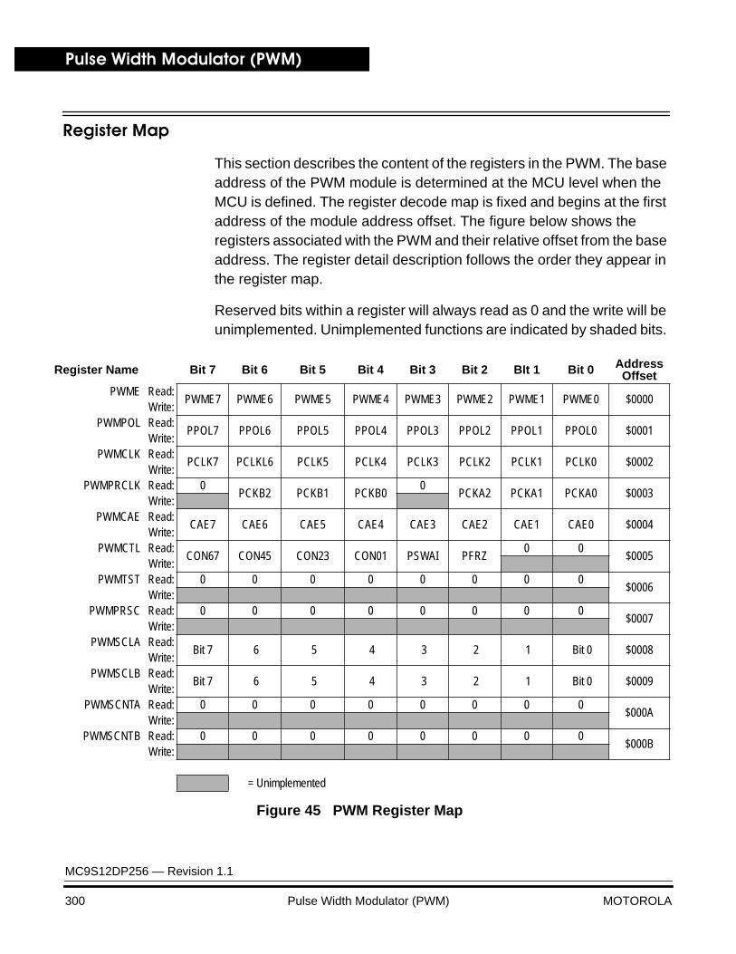
Pulse Width Modulator (PWM)
MC9S12DP256 — Revision 1.1
300 Pulse Width Modulator (PWM) MOTOROLA
Register Map
This section describes the content of the registers in the PWM. The base address of the PWM module is determined at the MCU level when the MCU is defined. The register decode map is fixed and begins at the first address of the module address offset. The figure below shows the registers associated with the PWM and their relative offset from the base address. The register detail description follows the order they appear in the register map.
Reserved bits within a register will always read as 0 and the write will be unimplemented. Unimplemented functions are indicated by shaded bits.
Register Name Bit 7 Bit 6 Bit 5 Bit 4 Bit 3 Bit 2 BIt 1 Bit 0 AddressOffset
PWME Read:PWME7 PWME6 PWME5 PWME4 PWME3 PWME2 PWME1 PWME0 $0000
Write:PWMPOL Read:
PPOL7 PPOL6 PPOL5 PPOL4 PPOL3 PPOL2 PPOL1 PPOL0 $0001Write:
PWMCLK Read:PCLK7 PCLKL6 PCLK5 PCLK4 PCLK3 PCLK2 PCLK1 PCLK0 $0002
Write:PWMPRCLK Read: 0
PCKB2 PCKB1 PCKB00
PCKA2 PCKA1 PCKA0 $0003Write:
PWMCAE Read:CAE7 CAE6 CAE5 CAE4 CAE3 CAE2 CAE1 CAE0 $0004
Write:PWMCTL Read:
CON67 CON45 CON23 CON01 PSWAI PFRZ0 0
$0005Write:
PWMTST Read: 0 0 0 0 0 0 0 0$0006
Write:PWMPRSC Read: 0 0 0 0 0 0 0 0
$0007Write:
PWMSCLA Read:Bit 7 6 5 4 3 2 1 Bit 0 $0008
Write:PWMSCLB Read:
Bit 7 6 5 4 3 2 1 Bit 0 $0009Write:
PWMSCNTA Read: 0 0 0 0 0 0 0 0$000A
Write:PWMSCNTB Read: 0 0 0 0 0 0 0 0
$000BWrite:
= Unimplemented
Figure 45 PWM Register Map
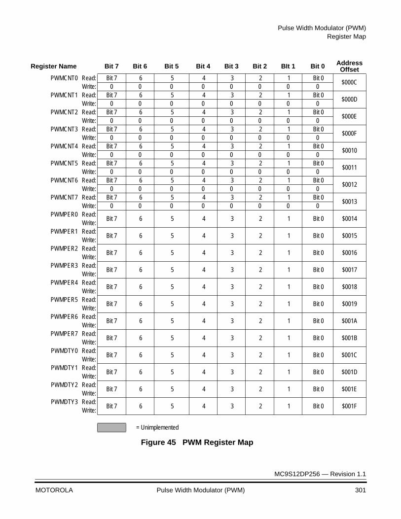
Pulse Width Modulator (PWM)Register Map
MC9S12DP256 — Revision 1.1
MOTOROLA Pulse Width Modulator (PWM) 301
PWMCNT0 Read: Bit 7 6 5 4 3 2 1 Bit 0 $000C
Write: 0 0 0 0 0 0 0 0PWMCNT1 Read: Bit 7 6 5 4 3 2 1 Bit 0
$000DWrite: 0 0 0 0 0 0 0 0
PWMCNT2 Read: Bit 7 6 5 4 3 2 1 Bit 0 $000E
Write: 0 0 0 0 0 0 0 0PWMCNT3 Read: Bit 7 6 5 4 3 2 1 Bit 0
$000FWrite: 0 0 0 0 0 0 0 0
PWMCNT4 Read: Bit 7 6 5 4 3 2 1 Bit 0 $0010
Write: 0 0 0 0 0 0 0 0PWMCNT5 Read: Bit 7 6 5 4 3 2 1 Bit 0
$0011Write: 0 0 0 0 0 0 0 0
PWMCNT6 Read: Bit 7 6 5 4 3 2 1 Bit 0 $0012
Write: 0 0 0 0 0 0 0 0PWMCNT7 Read: Bit 7 6 5 4 3 2 1 Bit 0
$0013Write: 0 0 0 0 0 0 0 0
PWMPER0 Read:Bit 7 6 5 4 3 2 1 Bit 0 $0014
Write:PWMPER1 Read:
Bit 7 6 5 4 3 2 1 Bit 0 $0015Write:
PWMPER2 Read:Bit 7 6 5 4 3 2 1 Bit 0 $0016
Write:PWMPER3 Read:
Bit 7 6 5 4 3 2 1 Bit 0 $0017Write:
PWMPER4 Read:Bit 7 6 5 4 3 2 1 Bit 0 $0018
Write:PWMPER5 Read:
Bit 7 6 5 4 3 2 1 Bit 0 $0019Write:
PWMPER6 Read:Bit 7 6 5 4 3 2 1 Bit 0 $001A
Write:PWMPER7 Read:
Bit 7 6 5 4 3 2 1 Bit 0 $001BWrite:
PWMDTY0 Read:Bit 7 6 5 4 3 2 1 Bit 0 $001C
Write:PWMDTY1 Read:
Bit 7 6 5 4 3 2 1 Bit 0 $001DWrite:
PWMDTY2 Read:Bit 7 6 5 4 3 2 1 Bit 0 $001E
Write:PWMDTY3 Read:
Bit 7 6 5 4 3 2 1 Bit 0 $001FWrite:
Register Name Bit 7 Bit 6 Bit 5 Bit 4 Bit 3 Bit 2 BIt 1 Bit 0 AddressOffset
= Unimplemented
Figure 45 PWM Register Map
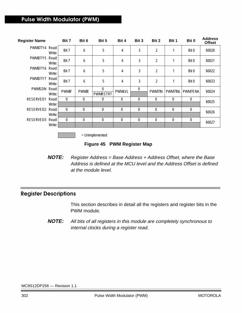
Pulse Width Modulator (PWM)
MC9S12DP256 — Revision 1.1
302 Pulse Width Modulator (PWM) MOTOROLA
NOTE: Register Address = Base Address + Address Offset, where the Base Address is defined at the MCU level and the Address Offset is defined at the module level.
Register Descriptions
This section describes in detail all the registers and register bits in the PWM module.
NOTE: All bits of all registers in this module are completely synchronous to internal clocks during a register read.
PWMDTY4 Read:Bit 7 6 5 4 3 2 1 Bit 0 $0020
Write:PWMDTY5 Read:
Bit 7 6 5 4 3 2 1 Bit 0 $0021Write:
PWMDTY6 Read:Bit 7 6 5 4 3 2 1 Bit 0 $0022
Write:PWMDTY7 Read:
Bit 7 6 5 4 3 2 1 Bit 0 $0023Write:
PWMSDN Read:PWMIF PWMIE
0PWMLVL
0PWM7IN PWM7INL PWM7ENA $0024
Write: PWMRSTRTRESERVED1 Read: 0 0 0 0 0 0 0 0
$0025Write:
RESERVED2 Read: 0 0 0 0 0 0 0 0$0026
Write:RESERVED3 Read: 0 0 0 0 0 0 0 0
$0027Write:
Register Name Bit 7 Bit 6 Bit 5 Bit 4 Bit 3 Bit 2 BIt 1 Bit 0 AddressOffset
= Unimplemented
Figure 45 PWM Register Map
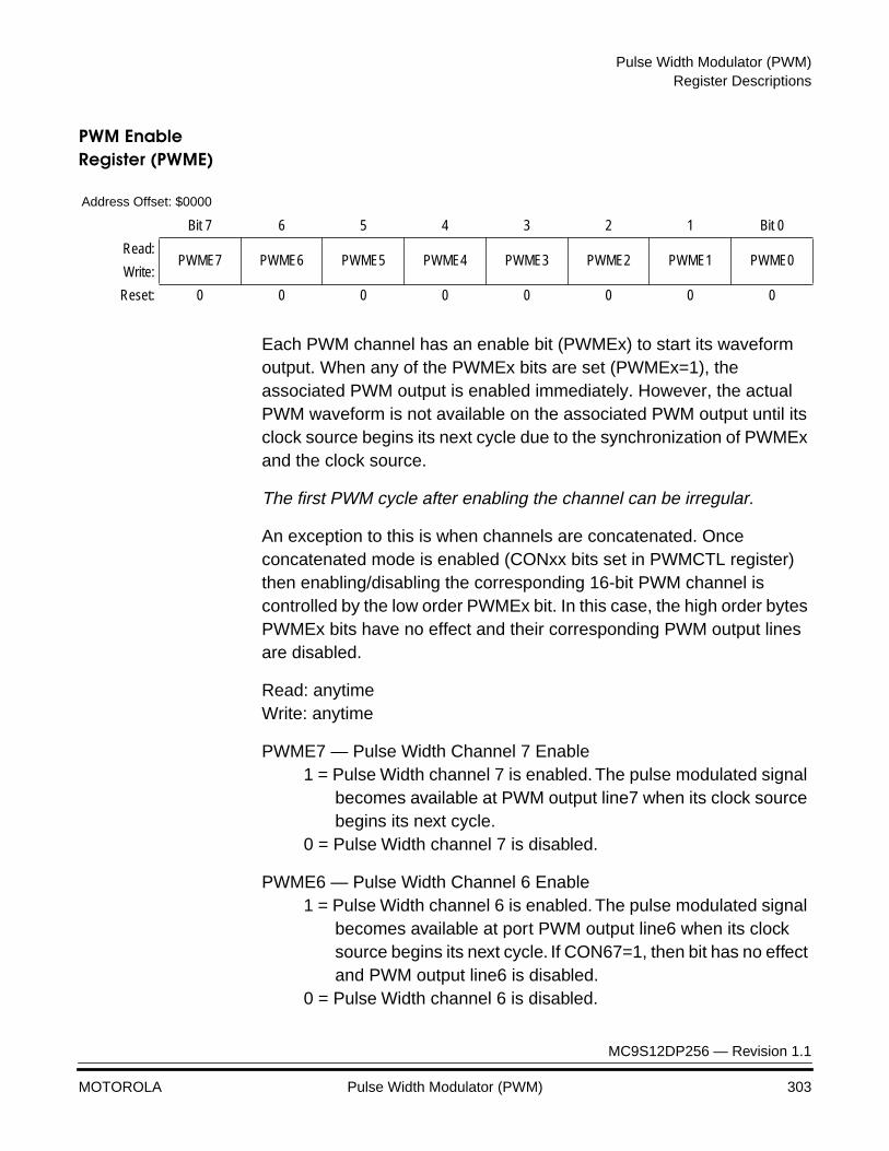
Pulse Width Modulator (PWM)Register Descriptions
MC9S12DP256 — Revision 1.1
MOTOROLA Pulse Width Modulator (PWM) 303
PWM Enable Register (PWME)
Each PWM channel has an enable bit (PWMEx) to start its waveform output. When any of the PWMEx bits are set (PWMEx=1), the associated PWM output is enabled immediately. However, the actual PWM waveform is not available on the associated PWM output until its clock source begins its next cycle due to the synchronization of PWMEx and the clock source.
The first PWM cycle after enabling the channel can be irregular.
An exception to this is when channels are concatenated. Once concatenated mode is enabled (CONxx bits set in PWMCTL register) then enabling/disabling the corresponding 16-bit PWM channel is controlled by the low order PWMEx bit. In this case, the high order bytes PWMEx bits have no effect and their corresponding PWM output lines are disabled.
Read: anytimeWrite: anytime
PWME7 — Pulse Width Channel 7 Enable1 = Pulse Width channel 7 is enabled. The pulse modulated signal
becomes available at PWM output line7 when its clock source begins its next cycle.
0 = Pulse Width channel 7 is disabled.
PWME6 — Pulse Width Channel 6 Enable1 = Pulse Width channel 6 is enabled. The pulse modulated signal
becomes available at port PWM output line6 when its clock source begins its next cycle. If CON67=1, then bit has no effect and PWM output line6 is disabled.
0 = Pulse Width channel 6 is disabled.
Address Offset: $0000
Bit 7 6 5 4 3 2 1 Bit 0
Read:PWME7 PWME6 PWME5 PWME4 PWME3 PWME2 PWME1 PWME0
Write:
Reset: 0 0 0 0 0 0 0 0

Pulse Width Modulator (PWM)
MC9S12DP256 — Revision 1.1
304 Pulse Width Modulator (PWM) MOTOROLA
PWME5 — Pulse Width Channel 5 Enable1 = Pulse Width channel 5 is enabled. The pulse modulated signal
becomes available at PWM, o/p bit 5 when its clock source begins its next cycle.
0 = Pulse Width channel 5 is disabled.
PWME4 — Pulse Width Channel 4 Enable1 = Pulse Width channel 4 is enabled. The pulse modulated signal
becomes available at PWM, o/p bit 4 when its clock source begins its next cycle. If CON45=1, then bit has no effect and PWM output line4 is disabled.
0 = Pulse Width channel 4 is disabled.
PWME3 — Pulse Width Channel 3 Enable1 = Pulse Width channel 3 is enabled. The pulse modulated signal
becomes available at PWM, o/p bit 3 when its clock source begins its next cycle.
0 = Pulse Width channel 3 is disabled.
PWME2 — Pulse Width Channel 2 Enable1 = Pulse Width channel 2 is enabled. The pulse modulated signal
becomes available at PWM, o/p bit 2 when its clock source begins its next cycle. If CON23=1, then bit has no effect and PWM output line2 is disabled.
0 = Pulse Width channel 2 is disabled.
PWME1 — Pulse Width Channel 1 Enable1 = Pulse Width channel 1 is enabled. The pulse modulated signal
becomes available at PWM, o/p bit 1 when its clock source begins its next cycle.
0 = Pulse Width channel 1 is disabled.
PWME0 — Pulse Width Channel 0 Enable1 = Pulse Width channel 0 is enabled. The pulse modulated signal
becomes available at PWM, o/p bit 0 when its clock source begins its next cycle. If CON01=1, then bit has no effect and PWM output line0 is disabled.
0 = Pulse Width channel 0 is disabled.
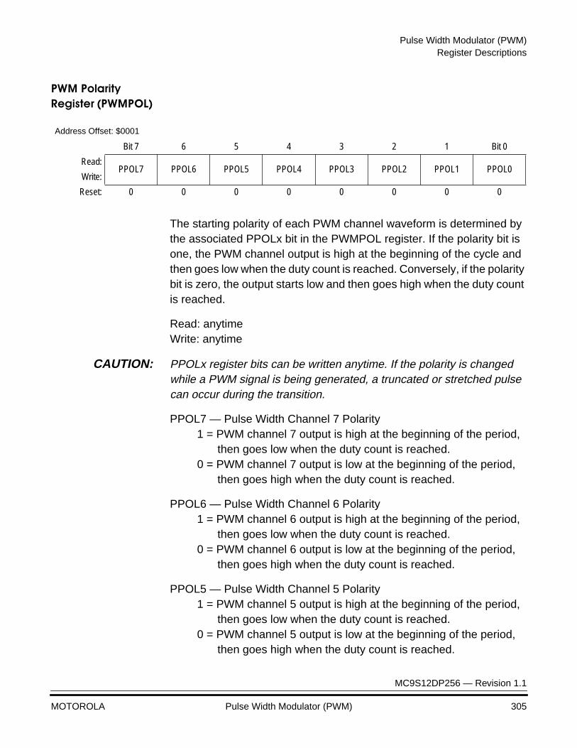
Pulse Width Modulator (PWM)Register Descriptions
MC9S12DP256 — Revision 1.1
MOTOROLA Pulse Width Modulator (PWM) 305
PWM Polarity Register (PWMPOL)
The starting polarity of each PWM channel waveform is determined by the associated PPOLx bit in the PWMPOL register. If the polarity bit is one, the PWM channel output is high at the beginning of the cycle and then goes low when the duty count is reached. Conversely, if the polarity bit is zero, the output starts low and then goes high when the duty count is reached.
Read: anytimeWrite: anytime
CAUTION: PPOLx register bits can be written anytime. If the polarity is changed while a PWM signal is being generated, a truncated or stretched pulse can occur during the transition.
PPOL7 — Pulse Width Channel 7 Polarity1 = PWM channel 7 output is high at the beginning of the period,
then goes low when the duty count is reached.0 = PWM channel 7 output is low at the beginning of the period,
then goes high when the duty count is reached.
PPOL6 — Pulse Width Channel 6 Polarity1 = PWM channel 6 output is high at the beginning of the period,
then goes low when the duty count is reached.0 = PWM channel 6 output is low at the beginning of the period,
then goes high when the duty count is reached.
PPOL5 — Pulse Width Channel 5 Polarity1 = PWM channel 5 output is high at the beginning of the period,
then goes low when the duty count is reached.0 = PWM channel 5 output is low at the beginning of the period,
then goes high when the duty count is reached.
Address Offset: $0001
Bit 7 6 5 4 3 2 1 Bit 0
Read:PPOL7 PPOL6 PPOL5 PPOL4 PPOL3 PPOL2 PPOL1 PPOL0
Write:
Reset: 0 0 0 0 0 0 0 0
Pulse Width Modulator (PWM)
MC9S12DP256 — Revision 1.1
306 Pulse Width Modulator (PWM) MOTOROLA
PPOL4 — Pulse Width Channel 4 Polarity1 = PWM channel 4 output is high at the beginning of the period,
then goes low when the duty count is reached.0 = PWM channel 4 output is low at the beginning of the period,
then goes high when the duty count is reached.
PPOL3 — Pulse Width Channel 3 Polarity1 = PWM channel 3 output is high at the beginning of the period,
then goes low when the duty count is reached.0 = PWM channel 3 output is low at the beginning of the period,
then goes high when the duty count is reached.
PPOL2 — Pulse Width Channel 2 Polarity1 = PWM channel 2 output is high at the beginning of the period,
then goes low when the duty count is reached.0 = PWM channel 2 output is low at the beginning of the period,
then goes high when the duty count is reached.
PPOL1 — Pulse Width Channel 1 Polarity1 = PWM channel 1 output is high at the beginning of the period,
then goes low when the duty count is reached.0 = PWM channel 1 output is low at the beginning of the period,
then goes high when the duty count is reached.
PPOL0 — Pulse Width Channel 0 Polarity1 = PWM channel 0 output is high at the beginning of the period,
then goes low when the duty count is reached.0 = PWM channel 0 output is low at the beginning of the period,
then goes high when the duty count is reached.
Pulse Width Modulator (PWM)Register Descriptions
MC9S12DP256 — Revision 1.1
MOTOROLA Pulse Width Modulator (PWM) 307
PWM Clock Select Register (PWMCLK)
Each PWM channel has a choice of two clocks to use as the clock source for that channel as described below.
Read: anytimeWrite: anytime
CAUTION: Register bits PCLK0 to PCLK7 can be written anytime. If a clock select is changed while a PWM signal is being generated, a truncated or stretched pulse can occur during the transition.
PCLK7 — Pulse Width Channel 7 Clock Select1 = Clock SB is the clock source for PWM channel 7.0 = Clock B is the clock source for PWM channel 7.
PCLK6 — Pulse Width Channel 6 Clock Select1 = Clock SB is the clock source for PWM channel 6.0 = Clock B is the clock source for PWM channel 6.
PCLK5 — Pulse Width Channel 5 Clock Select1 = Clock SA is the clock source for PWM channel 5.0 = Clock A is the clock source for PWM channel 5.
PCLK4 — Pulse Width Channel 4 Clock Select1 = Clock SA is the clock source for PWM channel 4.0 = Clock A is the clock source for PWM channel 4.
PCLK3 — Pulse Width Channel 3 Clock Select1 = Clock SB is the clock source for PWM channel 3.0 = Clock B is the clock source for PWM channel 3.
Address Offset: $0002
Bit 7 6 5 4 3 2 1 Bit 0
Read:PCLK7 PCLKL6 PCLK5 PCLK4 PCLK3 PCLK2 PCLK1 PCLK0
Write:
Reset: 0 0 0 0 0 0 0 0
Pulse Width Modulator (PWM)
MC9S12DP256 — Revision 1.1
308 Pulse Width Modulator (PWM) MOTOROLA
PCLK2 — Pulse Width Channel 2 Clock Select1 = Clock SB is the clock source for PWM channel 2.0 = Clock B is the clock source for PWM channel 2.
PCLK1 — Pulse Width Channel 1 Clock Select1 = Clock SA is the clock source for PWM channel 1.0 = Clock A is the clock source for PWM channel 1.
PCLK0 — Pulse Width Channel 0 Clock Select1 = Clock SA is the clock source for PWM channel 0.0 = Clock A is the clock source for PWM channel 0.
PWM Prescale Clock Select Register (PWMPRCLK)
This register selects the prescale clock source for clocks A and B independently.
Read: anytimeWrite: anytime
CAUTION: PCKB2–0 and PCKA2–0 register bits can be written anytime. If the clock pre-scale is changed while a PWM signal is being generated, a truncated or stretched pulse can occur during the transition.
PCKB2–PCKB0 — Prescaler Select for Clock B
Clock B is one of two clock sources which can be used for channels 2, 3, 6, or 7. These three bits determine the rate of clock B, as shown in the following table.
Address Offset: $0003
Bit 7 6 5 4 3 2 1 Bit 0
Read: 0PCKB2 PCKB1 PCKB0
0PCKA2 PCKA1 PCKA0
Write:
Reset: 0 0 0 0 0 0 0 0
= Reserved or unimplemented
Pulse Width Modulator (PWM)Register Descriptions
MC9S12DP256 — Revision 1.1
MOTOROLA Pulse Width Modulator (PWM) 309
PCKA2–PCKA0 — Prescaler Select for Clock A
Clock A is one of two clock sources which can be used for channels 0, 1, 4, or 5. These three bits determine the rate of clock A, as shown in the following table.
Table 50 Clock B Prescaler Selects
PCKB2 PCKB1 PCKB0 Value of Clock B
0 0 0 E
0 0 1 E / 2
0 1 0 E / 4
0 1 1 E / 8
1 0 0 E / 16
1 0 1 E / 32
1 1 0 E / 64
1 1 1 E / 128
Table 51 Clock A Prescaler Selects
PCKA2 PCKA1 PCKA0 Value of Clock A
0 0 0 E
0 0 1 E / 2
0 1 0 E / 4
0 1 1 E / 8
1 0 0 E / 16
1 0 1 E / 32
1 1 0 E / 64
1 1 1 E / 128
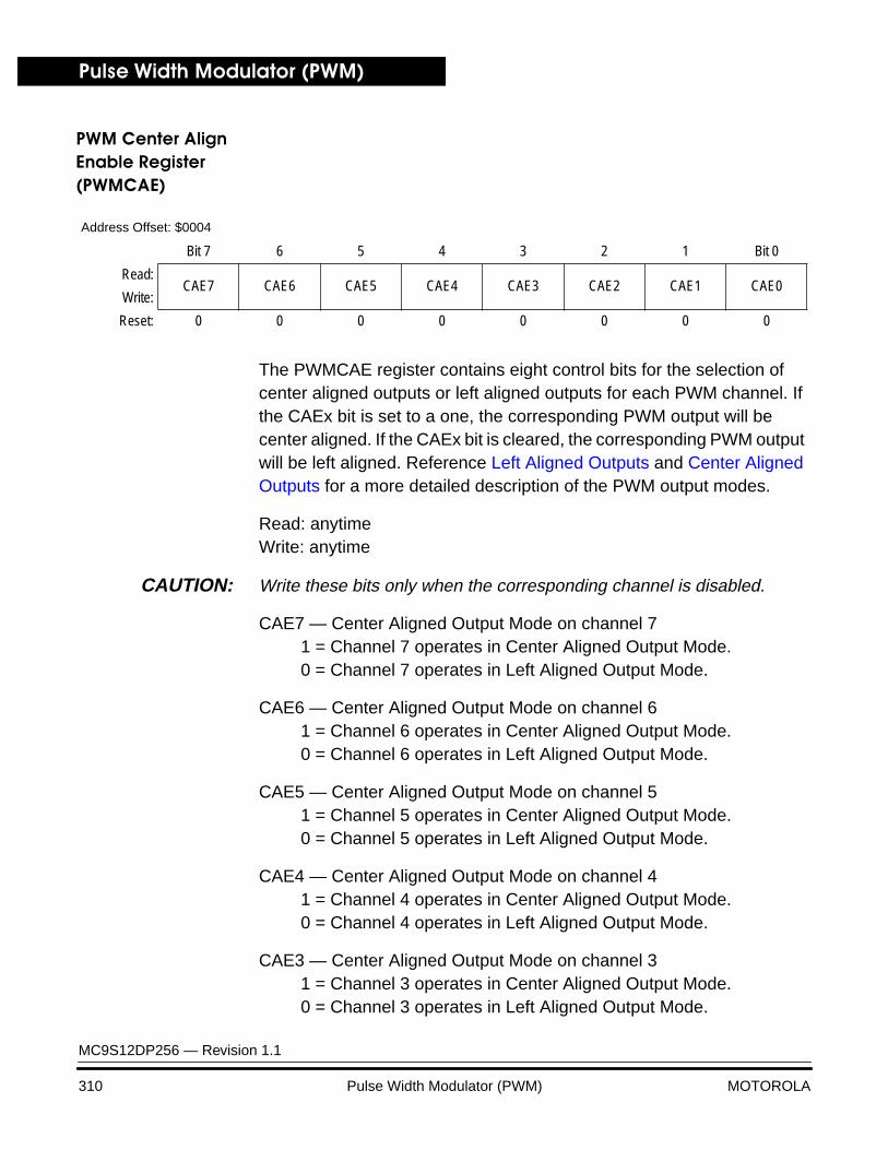
Pulse Width Modulator (PWM)
MC9S12DP256 — Revision 1.1
310 Pulse Width Modulator (PWM) MOTOROLA
PWM Center Align Enable Register (PWMCAE)
The PWMCAE register contains eight control bits for the selection of center aligned outputs or left aligned outputs for each PWM channel. If the CAEx bit is set to a one, the corresponding PWM output will be center aligned. If the CAEx bit is cleared, the corresponding PWM output will be left aligned. Reference Left Aligned Outputs and Center Aligned Outputs for a more detailed description of the PWM output modes.
Read: anytimeWrite: anytime
CAUTION: Write these bits only when the corresponding channel is disabled.
CAE7 — Center Aligned Output Mode on channel 71 = Channel 7 operates in Center Aligned Output Mode.0 = Channel 7 operates in Left Aligned Output Mode.
CAE6 — Center Aligned Output Mode on channel 61 = Channel 6 operates in Center Aligned Output Mode.0 = Channel 6 operates in Left Aligned Output Mode.
CAE5 — Center Aligned Output Mode on channel 51 = Channel 5 operates in Center Aligned Output Mode.0 = Channel 5 operates in Left Aligned Output Mode.
CAE4 — Center Aligned Output Mode on channel 41 = Channel 4 operates in Center Aligned Output Mode.0 = Channel 4 operates in Left Aligned Output Mode.
CAE3 — Center Aligned Output Mode on channel 31 = Channel 3 operates in Center Aligned Output Mode.0 = Channel 3 operates in Left Aligned Output Mode.
Address Offset: $0004
Bit 7 6 5 4 3 2 1 Bit 0
Read:CAE7 CAE6 CAE5 CAE4 CAE3 CAE2 CAE1 CAE0
Write:
Reset: 0 0 0 0 0 0 0 0
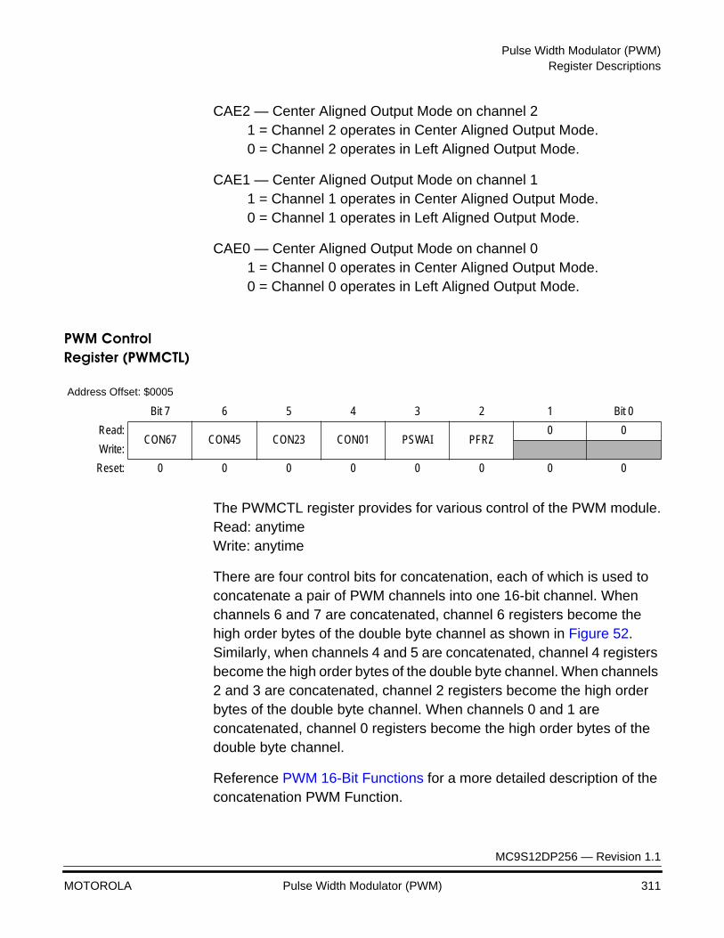
Pulse Width Modulator (PWM)Register Descriptions
MC9S12DP256 — Revision 1.1
MOTOROLA Pulse Width Modulator (PWM) 311
CAE2 — Center Aligned Output Mode on channel 21 = Channel 2 operates in Center Aligned Output Mode.0 = Channel 2 operates in Left Aligned Output Mode.
CAE1 — Center Aligned Output Mode on channel 11 = Channel 1 operates in Center Aligned Output Mode.0 = Channel 1 operates in Left Aligned Output Mode.
CAE0 — Center Aligned Output Mode on channel 01 = Channel 0 operates in Center Aligned Output Mode.0 = Channel 0 operates in Left Aligned Output Mode.
PWM Control Register (PWMCTL)
The PWMCTL register provides for various control of the PWM module.Read: anytimeWrite: anytime
There are four control bits for concatenation, each of which is used to concatenate a pair of PWM channels into one 16-bit channel. When channels 6 and 7 are concatenated, channel 6 registers become the high order bytes of the double byte channel as shown in Figure 52. Similarly, when channels 4 and 5 are concatenated, channel 4 registers become the high order bytes of the double byte channel. When channels 2 and 3 are concatenated, channel 2 registers become the high order bytes of the double byte channel. When channels 0 and 1 are concatenated, channel 0 registers become the high order bytes of the double byte channel.
Reference PWM 16-Bit Functions for a more detailed description of the concatenation PWM Function.
Address Offset: $0005
Bit 7 6 5 4 3 2 1 Bit 0
Read:CON67 CON45 CON23 CON01 PSWAI PFRZ
0 0
Write:
Reset: 0 0 0 0 0 0 0 0
Pulse Width Modulator (PWM)
MC9S12DP256 — Revision 1.1
312 Pulse Width Modulator (PWM) MOTOROLA
CAUTION: Change these bits only when both corresponding channels are disabled.
CON67 — Concatenate channels 6 and 71 = Channels 6 and 7 are concatenated to create one 16-bit PWM
channel. Channel 6 becomes the high order byte and channel 7 becomes the low order byte. Channel 7 output pin is used as the output for this 16-bit PWM (bit 7 of port PWMP). Channel 7 clock select control-bit determines the clock source, channel 7 polarity bit determines the polarity, channel 7 enable bit enables the output and channel 7 center aligned enable bit determines the output mode.
0 = Channels 6 and 7 are separate 8-bit PWMs.
CON45 — Concatenate channels 4 and 51 = Channels 4 and 5 are concatenated to create one 16-bit PWM
channel. Channel 4 becomes the high order byte and channel 5 becomes the low order byte. Channel 5 output pin is used as the output for this 16-bit PWM (bit 5 of port PWMP). Channel 5 clock select control-bit determines the clock source, channel 5 polarity bit determines the polarity, channel 5 enable bit enables the output and channel 5 center aligned enable bit determines the output mode.
0 = Channels 4 and 5 are separate 8-bit PWMs.
CON23 — Concatenate channels 2 and 31 = Channels 2 and 3 are concatenated to create one 16-bit PWM
channel. Channel 2 becomes the high order byte and channel 3 becomes the low order byte. Channel 3 output pin is used as the output for this 16-bit PWM (bit 3 of port PWMP). Channel 3 clock select control-bit determines the clock source, channel 3 polarity bit determines the polarity, channel 3 enable bit enables the output and channel 3 center aligned enable bit determines the output mode.
0 = Channels 2 and 3 are separate 8-bit PWMs.
CON01 — Concatenate channels 0 and 11 = Channels 0 and 1 are concatenated to create one 16-bit PWM
channel. Channel 0 becomes the high order byte and channel 1 becomes the low order byte. Channel 1 output pin is used as
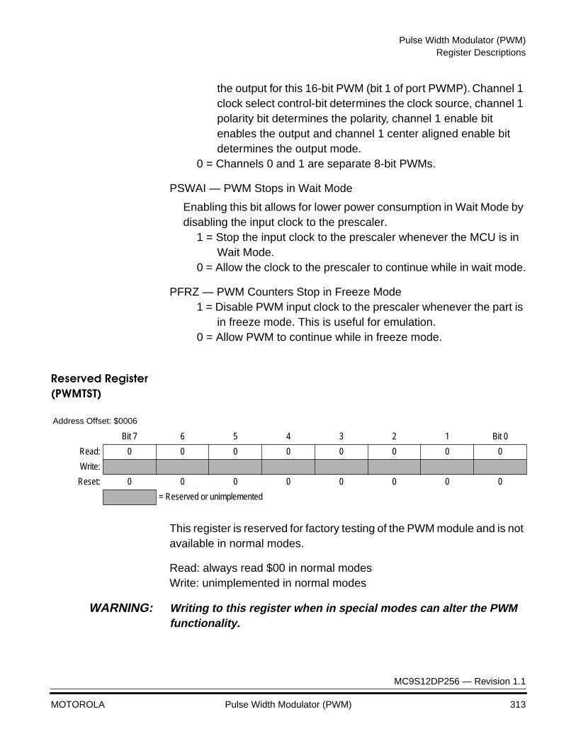
Pulse Width Modulator (PWM)Register Descriptions
MC9S12DP256 — Revision 1.1
MOTOROLA Pulse Width Modulator (PWM) 313
the output for this 16-bit PWM (bit 1 of port PWMP). Channel 1 clock select control-bit determines the clock source, channel 1 polarity bit determines the polarity, channel 1 enable bit enables the output and channel 1 center aligned enable bit determines the output mode.
0 = Channels 0 and 1 are separate 8-bit PWMs.
PSWAI — PWM Stops in Wait Mode
Enabling this bit allows for lower power consumption in Wait Mode by disabling the input clock to the prescaler.
1 = Stop the input clock to the prescaler whenever the MCU is in Wait Mode.
0 = Allow the clock to the prescaler to continue while in wait mode.
PFRZ — PWM Counters Stop in Freeze Mode1 = Disable PWM input clock to the prescaler whenever the part is
in freeze mode. This is useful for emulation.0 = Allow PWM to continue while in freeze mode.
Reserved Register (PWMTST)
This register is reserved for factory testing of the PWM module and is not available in normal modes.
Read: always read $00 in normal modesWrite: unimplemented in normal modes
WARNING: Writing to this register when in special modes can alter the PWM functionality.
Address Offset: $0006
Bit 7 6 5 4 3 2 1 Bit 0
Read: 0 0 0 0 0 0 0 0
Write:
Reset: 0 0 0 0 0 0 0 0
= Reserved or unimplemented
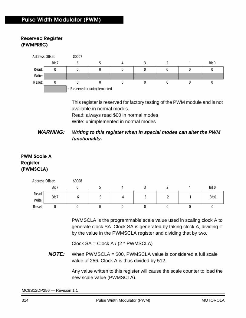
Pulse Width Modulator (PWM)
MC9S12DP256 — Revision 1.1
314 Pulse Width Modulator (PWM) MOTOROLA
Reserved Register (PWMPRSC)
This register is reserved for factory testing of the PWM module and is not available in normal modes.Read: always read $00 in normal modesWrite: unimplemented in normal modes
WARNING: Writing to this register when in special modes can alter the PWM functionality.
PWM Scale A Register (PWMSCLA)
PWMSCLA is the programmable scale value used in scaling clock A to generate clock SA. Clock SA is generated by taking clock A, dividing it by the value in the PWMSCLA register and dividing that by two.
Clock SA = Clock A / (2 * PWMSCLA)
NOTE: When PWMSCLA = $00, PWMSCLA value is considered a full scale value of 256. Clock A is thus divided by 512.
Any value written to this register will cause the scale counter to load the new scale value (PWMSCLA).
Address Offset: $0007
Bit 7 6 5 4 3 2 1 Bit 0
Read: 0 0 0 0 0 0 0 0
Write:
Reset: 0 0 0 0 0 0 0 0
= Reserved or unimplemented
Address Offset: $0008
Bit 7 6 5 4 3 2 1 Bit 0
Read:Bit 7 6 5 4 3 2 1 Bit 0
Write:
Reset: 0 0 0 0 0 0 0 0
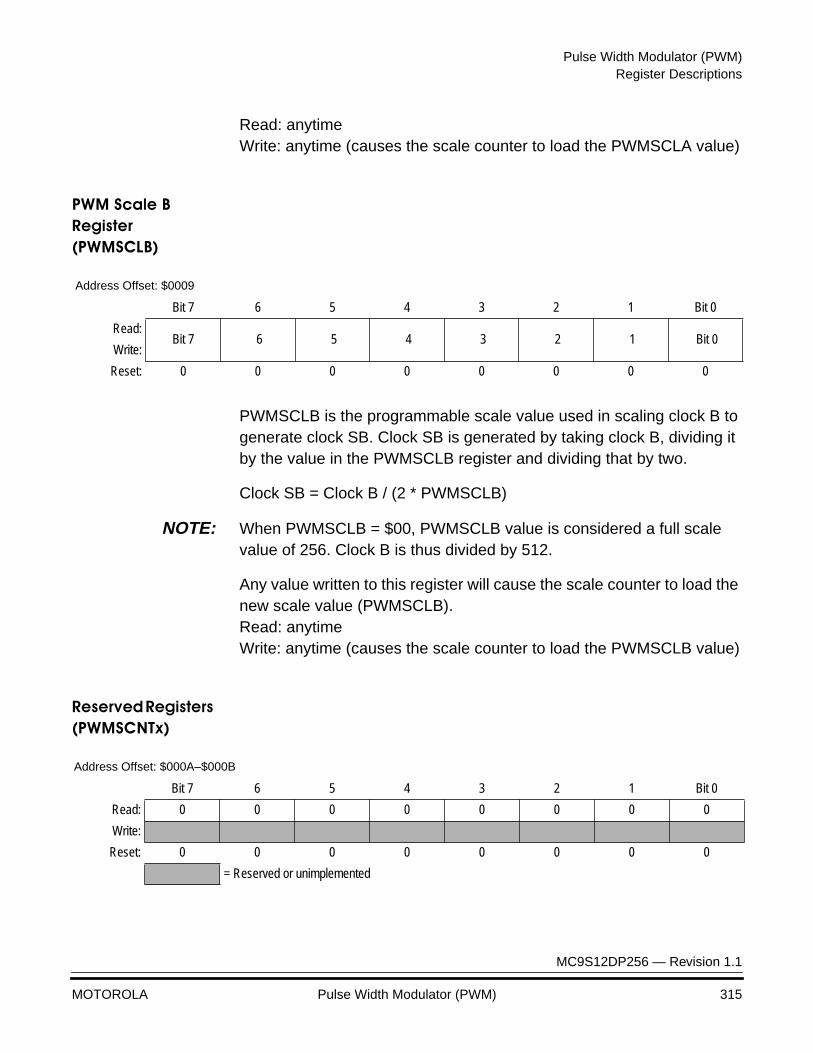
Pulse Width Modulator (PWM)Register Descriptions
MC9S12DP256 — Revision 1.1
MOTOROLA Pulse Width Modulator (PWM) 315
Read: anytimeWrite: anytime (causes the scale counter to load the PWMSCLA value)
PWM Scale B Register (PWMSCLB)
PWMSCLB is the programmable scale value used in scaling clock B to generate clock SB. Clock SB is generated by taking clock B, dividing it by the value in the PWMSCLB register and dividing that by two.
Clock SB = Clock B / (2 * PWMSCLB)
NOTE: When PWMSCLB = $00, PWMSCLB value is considered a full scale value of 256. Clock B is thus divided by 512.
Any value written to this register will cause the scale counter to load the new scale value (PWMSCLB).Read: anytimeWrite: anytime (causes the scale counter to load the PWMSCLB value)
Reserved Registers (PWMSCNTx)
Address Offset: $0009
Bit 7 6 5 4 3 2 1 Bit 0
Read:Bit 7 6 5 4 3 2 1 Bit 0
Write:
Reset: 0 0 0 0 0 0 0 0
Address Offset: $000A–$000B
Bit 7 6 5 4 3 2 1 Bit 0
Read: 0 0 0 0 0 0 0 0
Write:
Reset: 0 0 0 0 0 0 0 0
= Reserved or unimplemented
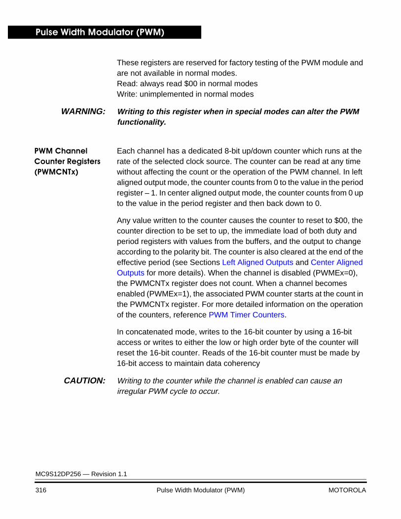
Pulse Width Modulator (PWM)
MC9S12DP256 — Revision 1.1
316 Pulse Width Modulator (PWM) MOTOROLA
These registers are reserved for factory testing of the PWM module and are not available in normal modes.Read: always read $00 in normal modesWrite: unimplemented in normal modes
WARNING: Writing to this register when in special modes can alter the PWM functionality.
PWM Channel Counter Registers (PWMCNTx)
Each channel has a dedicated 8-bit up/down counter which runs at the rate of the selected clock source. The counter can be read at any time without affecting the count or the operation of the PWM channel. In left aligned output mode, the counter counts from 0 to the value in the period register – 1. In center aligned output mode, the counter counts from 0 up to the value in the period register and then back down to 0.
Any value written to the counter causes the counter to reset to $00, the counter direction to be set to up, the immediate load of both duty and period registers with values from the buffers, and the output to change according to the polarity bit. The counter is also cleared at the end of the effective period (see Sections Left Aligned Outputs and Center Aligned Outputs for more details). When the channel is disabled (PWMEx=0), the PWMCNTx register does not count. When a channel becomes enabled (PWMEx=1), the associated PWM counter starts at the count in the PWMCNTx register. For more detailed information on the operation of the counters, reference PWM Timer Counters.
In concatenated mode, writes to the 16-bit counter by using a 16-bit access or writes to either the low or high order byte of the counter will reset the 16-bit counter. Reads of the 16-bit counter must be made by 16-bit access to maintain data coherency
CAUTION: Writing to the counter while the channel is enabled can cause an irregular PWM cycle to occur.

Pulse Width Modulator (PWM)Register Descriptions
MC9S12DP256 — Revision 1.1
MOTOROLA Pulse Width Modulator (PWM) 317
Read: anytimeWrite: anytime (any value written causes PWM counter to be reset to $00)
Bit 7 6 5 4 3 2 1 Bit 0
Address $000C PWMCNT0
Read: Bit 7 6 5 4 3 2 1 Bit 0
Write: 0 0 0 0 0 0 0 0
Reset: 0 0 0 0 0 0 0 0
Address $000D PWMCNT1
Read: Bit 7 6 5 4 3 2 1 Bit 0
Write: 0 0 0 0 0 0 0 0
Reset: 0 0 0 0 0 0 0 0
Address $000E PWMCNT2
Read: Bit 7 6 5 4 3 2 1 Bit 0
Write: 0 0 0 0 0 0 0 0
Reset: 0 0 0 0 0 0 0 0
Address $000F PWMCNT3
Read: Bit 7 6 5 4 3 2 1 Bit 0
Write: 0 0 0 0 0 0 0 0
Reset: 0 0 0 0 0 0 0 0
Address $0010 PWMCNT4
Read: Bit 7 6 5 4 3 2 1 Bit 0
Write: 0 0 0 0 0 0 0 0
Reset: 0 0 0 0 0 0 0 0
Address $0011 PWMCNT5
Read: Bit 7 6 5 4 3 2 1 Bit 0
Write: 0 0 0 0 0 0 0 0
Reset: 0 0 0 0 0 0 0 0
Address $0012 PWMCNT6
Read: Bit 7 6 5 4 3 2 1 Bit 0
Write: 0 0 0 0 0 0 0 0
Reset: 0 0 0 0 0 0 0 0
Address $0013 PWMCNT7
Read: Bit 7 6 5 4 3 2 1 Bit 0
Write: 0 0 0 0 0 0 0 0
Reset: 0 0 0 0 0 0 0 0
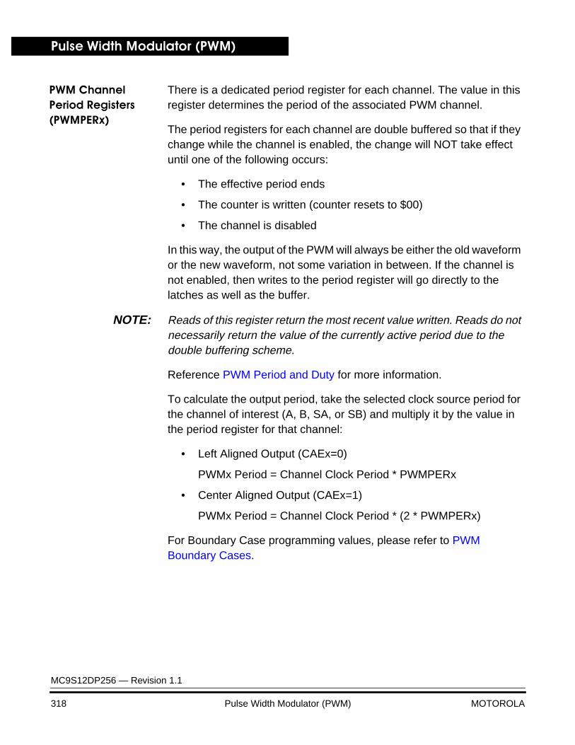
Pulse Width Modulator (PWM)
MC9S12DP256 — Revision 1.1
318 Pulse Width Modulator (PWM) MOTOROLA
PWM Channel Period Registers (PWMPERx)
There is a dedicated period register for each channel. The value in this register determines the period of the associated PWM channel.
The period registers for each channel are double buffered so that if they change while the channel is enabled, the change will NOT take effect until one of the following occurs:
• The effective period ends
• The counter is written (counter resets to $00)
• The channel is disabled
In this way, the output of the PWM will always be either the old waveform or the new waveform, not some variation in between. If the channel is not enabled, then writes to the period register will go directly to the latches as well as the buffer.
NOTE: Reads of this register return the most recent value written. Reads do not necessarily return the value of the currently active period due to the double buffering scheme.
Reference PWM Period and Duty for more information.
To calculate the output period, take the selected clock source period for the channel of interest (A, B, SA, or SB) and multiply it by the value in the period register for that channel:
• Left Aligned Output (CAEx=0)
PWMx Period = Channel Clock Period * PWMPERx
• Center Aligned Output (CAEx=1)
PWMx Period = Channel Clock Period * (2 * PWMPERx)
For Boundary Case programming values, please refer to PWM Boundary Cases.
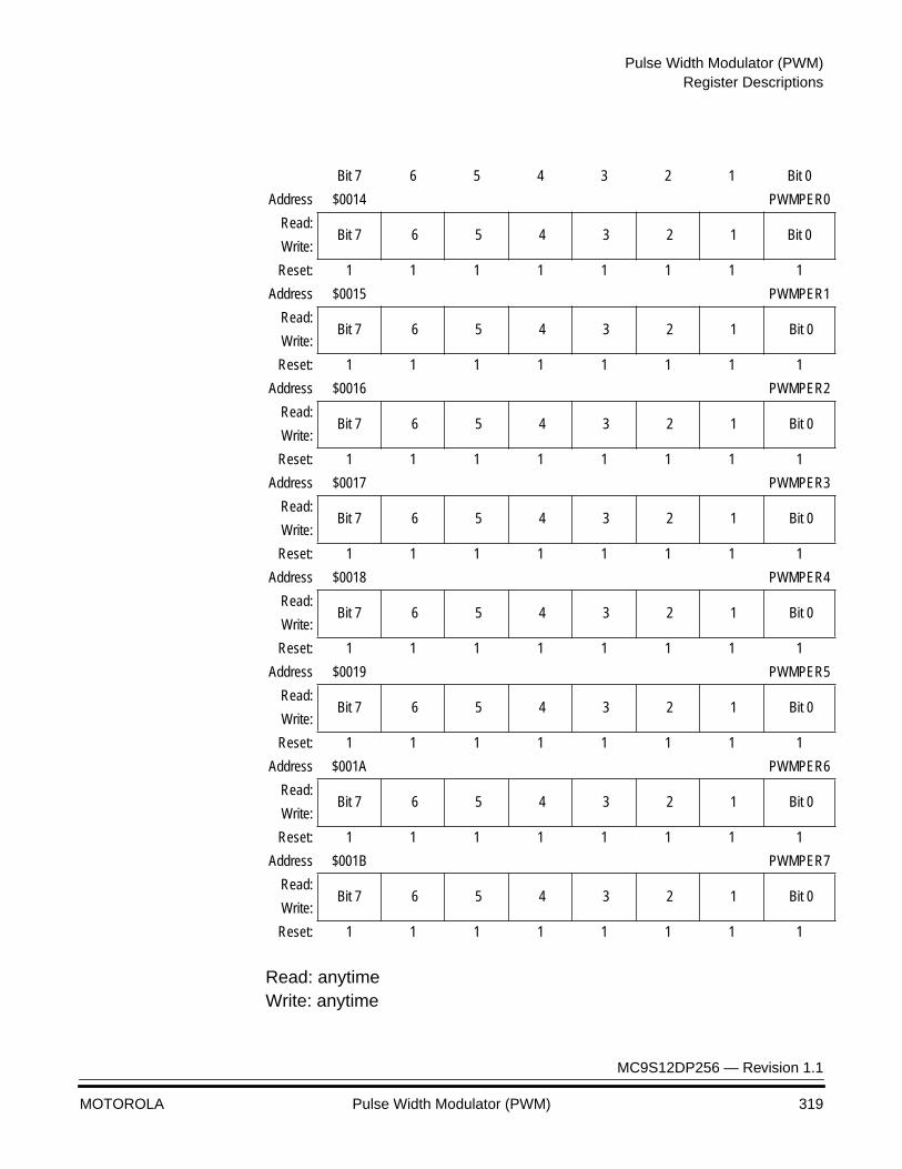
Pulse Width Modulator (PWM)Register Descriptions
MC9S12DP256 — Revision 1.1
MOTOROLA Pulse Width Modulator (PWM) 319
Read: anytimeWrite: anytime
Bit 7 6 5 4 3 2 1 Bit 0
Address $0014 PWMPER0
Read:Bit 7 6 5 4 3 2 1 Bit 0
Write:
Reset: 1 1 1 1 1 1 1 1
Address $0015 PWMPER1
Read:Bit 7 6 5 4 3 2 1 Bit 0
Write:
Reset: 1 1 1 1 1 1 1 1
Address $0016 PWMPER2
Read:Bit 7 6 5 4 3 2 1 Bit 0
Write:
Reset: 1 1 1 1 1 1 1 1
Address $0017 PWMPER3
Read:Bit 7 6 5 4 3 2 1 Bit 0
Write:
Reset: 1 1 1 1 1 1 1 1
Address $0018 PWMPER4
Read:Bit 7 6 5 4 3 2 1 Bit 0
Write:
Reset: 1 1 1 1 1 1 1 1
Address $0019 PWMPER5
Read:Bit 7 6 5 4 3 2 1 Bit 0
Write:
Reset: 1 1 1 1 1 1 1 1
Address $001A PWMPER6
Read:Bit 7 6 5 4 3 2 1 Bit 0
Write:
Reset: 1 1 1 1 1 1 1 1
Address $001B PWMPER7
Read:Bit 7 6 5 4 3 2 1 Bit 0
Write:
Reset: 1 1 1 1 1 1 1 1

Pulse Width Modulator (PWM)
MC9S12DP256 — Revision 1.1
320 Pulse Width Modulator (PWM) MOTOROLA
PWM Channel Duty Registers (PWMDTYx)
There is a dedicated duty register for each channel. The value in this register determines the duty of the associated PWM channel. The duty value is compared to the counter and if it is equal to the counter value a match occurs and the output changes state.
The duty registers for each channel are double buffered so that if they change while the channel is enabled, the change will NOT take effect until one of the following occurs:
• The effective period ends
• The counter is written (counter resets to $00)
• The channel is disabled
In this way, the output of the PWM will always be either the old duty waveform or the new duty waveform, not some variation in between. If the channel is not enabled, then writes to the duty register will go directly to the latches as well as the buffer.
NOTE: Reads of this register return the most recent value written. Reads do not necessarily return the value of the currently active duty due to the double buffering scheme.
Reference PWM Period and Duty for more information.
NOTE: Depending on the polarity bit, the duty registers will contain the count of either the high time or the low time. If the polarity bit is one, the output starts high and then goes low when the duty count is reached, so the duty registers contain a count of the high time. If the polarity bit is zero, the output starts low and then goes high when the duty count is reached, so the duty registers contain a count of the low time.
To calculate the output duty cycle (high time as a % of period) for a particular channel:
• Polarity = 0 (PPOLx=0)
Duty Cycle = [(PWMPERx-PWMDTYx)/PWMPERx] * 100%
• Polarity = 1 (PPOLx=1)
Duty Cycle = [PWMDTYx / PWMPERx] * 100%

Pulse Width Modulator (PWM)Register Descriptions
MC9S12DP256 — Revision 1.1
MOTOROLA Pulse Width Modulator (PWM) 321
For Boundary Case programming values, please refer to PWM Boundary Cases.
Read: anytimeWrite: anytime
Bit 7 6 5 4 3 2 1 Bit 0
Address $001C PWMDTY0
Read:Bit 7 6 5 4 3 2 1 Bit 0
Write:
Reset: 1 1 1 1 1 1 1 1
Address $001D PWMDTY1
Read:Bit 7 6 5 4 3 2 1 Bit 0
Write:
Reset: 1 1 1 1 1 1 1 1
Address $001E PWMDTY2
Read:Bit 7 6 5 4 3 2 1 Bit 0
Write:
Reset: 1 1 1 1 1 1 1 1
Address $001F PWMDTY3
Read:Bit 7 6 5 4 3 2 1 Bit 0
Write:
Reset: 1 1 1 1 1 1 1 1
Address $0020 PWMDTY4
Read:Bit 7 6 5 4 3 2 1 Bit 0
Write:
Reset: 1 1 1 1 1 1 1 1
Address $0021 PWMDTY5
Read:Bit 7 6 5 4 3 2 1 Bit 0
Write:
Reset: 1 1 1 1 1 1 1 1
Address $0022 PWMDTY6
Read:Bit 7 6 5 4 3 2 1 Bit 0
Write:
Reset: 1 1 1 1 1 1 1 1
Address $0023 PWMDTY7
Read:Bit 7 6 5 4 3 2 1 Bit 0
Write:
Reset: 1 1 1 1 1 1 1 1
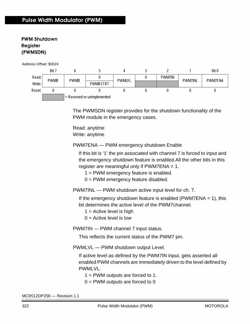
Pulse Width Modulator (PWM)
MC9S12DP256 — Revision 1.1
322 Pulse Width Modulator (PWM) MOTOROLA
PWM Shutdown Register (PWMSDN)
The PWMSDN register provides for the shutdown functionality of the PWM module in the emergency cases.
Read: anytimeWrite: anytime
PWM7ENA — PWM emergency shutdown Enable
If this bit is ‘1’ the pin associated with channel 7 is forced to input and the emergency shutdown feature is enabled.All the other bits in this register are meaningful only if PWM7ENA = 1.
1 = PWM emergency feature is enabled.0 = PWM emergency feature disabled.
PWM7INL — PWM shutdown active input level for ch. 7.
If the emergency shutdown feature is enabled (PWM7ENA = 1), this bit determines the active level of the PWM7channel.
1 = Active level is high0 = Active level is low
PWM7IN — PWM channel 7 input status.
This reflects the current status of the PWM7 pin.
PWMLVL — PWM shutdown output Level.
If active level as defined by the PWM7IN input, gets asserted all enabled PWM channels are immediately driven to the level defined by PWMLVL.
1 = PWM outputs are forced to 1.0 = PWM outputs are forced to 0
Address Offset: $0024
Bit 7 6 5 4 3 2 1 Bit 0
Read:PWMIF PWMIE
0PWMLVL
0 PWM7INPWM7INL PWM7ENA
Write: PWMRSTRT
Reset: 0 0 0 0 0 0 0 0
= Reserved or unimplemented
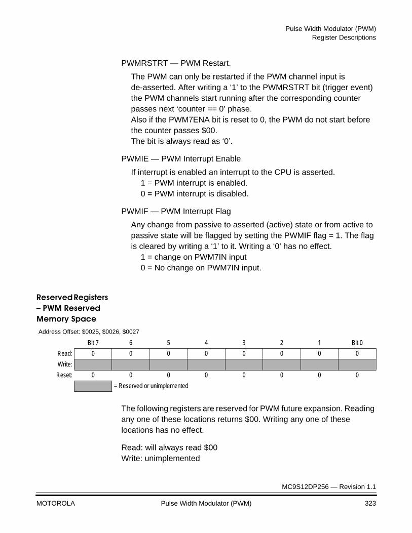
Pulse Width Modulator (PWM)Register Descriptions
MC9S12DP256 — Revision 1.1
MOTOROLA Pulse Width Modulator (PWM) 323
PWMRSTRT — PWM Restart.
The PWM can only be restarted if the PWM channel input is de-asserted. After writing a ‘1’ to the PWMRSTRT bit (trigger event) the PWM channels start running after the corresponding counter passes next ‘counter == 0’ phase. Also if the PWM7ENA bit is reset to 0, the PWM do not start before the counter passes $00.The bit is always read as ‘0’.
PWMIE — PWM Interrupt Enable
If interrupt is enabled an interrupt to the CPU is asserted.1 = PWM interrupt is enabled.0 = PWM interrupt is disabled.
PWMIF — PWM Interrupt Flag
Any change from passive to asserted (active) state or from active to passive state will be flagged by setting the PWMIF flag = 1. The flag is cleared by writing a ‘1’ to it. Writing a ‘0’ has no effect.
1 = change on PWM7IN input0 = No change on PWM7IN input.
Reserved Registers Ð PWM Reserved Memory Space
The following registers are reserved for PWM future expansion. Reading any one of these locations returns $00. Writing any one of these locations has no effect.
Read: will always read $00Write: unimplemented
Address Offset: $0025, $0026, $0027
Bit 7 6 5 4 3 2 1 Bit 0
Read: 0 0 0 0 0 0 0 0
Write:
Reset: 0 0 0 0 0 0 0 0
= Reserved or unimplemented
Pulse Width Modulator (PWM)
MC9S12DP256 — Revision 1.1
324 Pulse Width Modulator (PWM) MOTOROLA
Functional Description
PWM Clock Select There are four available clocks called clock A, clock B, clock SA (Scaled A), and clock SB (Scaled B). These four clocks are based on the clock, E Clock which runs at the same frequency as the IP bus clock ipg_clock.
NOTE: All E Clock (E) references within this document are used to refer only to the frequency and do not suggest that this clock is actually used in implementation.
For the MC9S12DP256, E clock is same as the ipg_clk. So all reference to E clock in this document are to be read as ipg_clk.
Clock A and B can be software selected to be E, E/2, E/4, E/8,..., E/64, E/128. Clock SA uses clock A as an input and divides it further with a reloadable counter. Similarly, Clock SB uses clock B as an input and divides it further with a reloadable counter. The rates available for clock SA are software selectable to be clock A divided by 2, 4, 6, 8, ..., or 512 in increments of divide by 2. Similar rates are available for clock SB. Each PWM channel has the capability of selecting one of two clocks, either the pre-scaled clock (clock A or B) or the scaled clock (clock SA or SB).
The block diagram in Figure 46 shows the four different clocks and how the scaled clocks are created.

Pulse Width Modulator (PWM)Functional Description
MC9S12DP256 — Revision 1.1
MOTOROLA Pulse Width Modulator (PWM) 325
Figure 46 PWM Clock Select Block Diagram
24
816
3264
128
PCK
B2
PCK
B1
PCK
B0
M
U
X
Clock A
Clock B
Clock SA
Clock A/2, A/4, A/6,....A/512
PRESCALE SCALE
Divi
de b
y Pr
esca
ler T
aps:
PFR
Zfip
g_fr
eeze
ipg_
cloc
k
CLOCK SELECT
MUX
PCLK0
Clock toPWM Ch 0
MUX
PCLK2
Clock toPWM Ch 2
MUX
PCLK1
Clock toPWM Ch 1
MUX
PCLK4
Clock toPWM Ch 4
MUX
PCLK5
Clock toPWM Ch 5
MUX
PCLK6
Clock toPWM Ch 6
MUX
PCLK7
Clock toPWM Ch 7
MUX
PCLK3
Clock toPWM Ch 3
Load
DIV 2PWMSCLB
8-bit Down Counter
Clock SB
Clock B/2, B/4, B/6,....B/512
M
U
X
PCK
A2
PCK
A1
PCK
A0
PWM
E7-0
Count=1
Load
DIV 2PWMSCLA
8-bit Down Counter Count=1
Pulse Width Modulator (PWM)
MC9S12DP256 — Revision 1.1
326 Pulse Width Modulator (PWM) MOTOROLA
Prescale The input clock to the PWM prescaler is the bus clock. It can be disabled whenever the part is in freeze mode by setting the PFRZ bit in the PWMCTL register. If this bit is set, whenever the MCU is in freeze mode (ipg_freeze active) the input clock to the prescaler is disabled. This is useful for emulation in order to freeze the PWM. The input clock can also be disabled when all eight PWM channels are disabled (PWME7–0=0). This is useful for reducing power by disabling the prescale counter.
Clock A and clock B are scaled values of the input clock. The value is software selectable for both clock A and clock B and has options of E, E/2, E/4, E/8, E/16, E/32, E/64, or E/128. The value selected for clock A is determined by the PCKA2, PCKA1, PCKA0 bits in the PWMPRCLK register. The value selected for clock B is determined by the PCKB2, PCKB1, PCKB0 bits also in the PWMPRCLK register.
Clock Scale The scaled A clock uses clock A as an input and divides it further with a user programmable value and then divides this by 2. The scaled B clock uses clock B as an input and divides it further with a user programmable value and then divides this by 2. The rates available for clock SA are software selectable to be clock A divided by 2, 4, 6, 8, ..., or 512 in increments of divide by 2. Similar rates are available for clock SB.
Clock A is used as an input to an 8-bit down counter. This down counter loads a user programmable scale value from the scale register (PWMSCLA). When the down counter reaches one, two things happen; a pulse is output and the 8-bit counter is re-loaded. The output signal from this circuit is further divided by two. This gives a greater range with only a slight reduction in granularity. Clock SA equals Clock A divided by two times the value in the PWMSCLA register.
NOTE: Clock SA = Clock A / (2 * PWMSCLA)
When PWMSCLA = $00, PWMSCLA value is considered a full scale value of 256. Clock A is thus divided by 512.
Similarly, Clock B is used as an input to an 8-bit down counter followed by a divide by two producing clock SB. Thus, clock SB equals Clock B divided by two times the value in the PWMSCLB register.
NOTE: Clock SB = Clock B / (2 * PWMSCLB)

Pulse Width Modulator (PWM)Functional Description
MC9S12DP256 — Revision 1.1
MOTOROLA Pulse Width Modulator (PWM) 327
When PWMSCLB = $00, PWMSCLB value is considered a full scale value of 256. Clock B is thus divided by 512.
As an example, consider the case in which the user writes $FF into the PWMSCLA register. Clock A for this case will be E divided by 4. A pulse will occur at a rate of once every 255x4 E cycles. Passing this through the divide by two circuit produces a clock signal at an E divided by 2040 rate. Similarly, a value of $01 in the PWMSCLA register when clock A is E divided by 4 will produce a clock at an E divided by 8 rate.
Writing to PWMSCLA or PWMSCLB causes the associated 8-bit down counter to be re-loaded. Otherwise, when changing rates the counter would have to count down to $01 before counting at the proper rate. Forcing the associated counter to re-load the scale register value every time PWMSCLA or PWMSCLB is written prevents this.
CAUTION: Writing to the scale registers while channels are operating can cause irregularities in the PWM outputs.
Clock Select Each PWM channel has the capability of selecting one of two clocks. For channels 0, 1, 4, and 5 the clock choices are clock A or clock SA. For channels 2, 3, 6, and 7 the choices are clock B or clock SB. The clock selection is done with the PCLKx control bits in the PWMCLK register.
CAUTION: Changing clock control bits while channels are operating can cause irregularities in the PWM outputs.
PWM Channel Timers
The main part of the PWM module are the actual timers. Each of the timer channels has a counter, a period register and a duty register (each are 8-bit). The waveform output period is controlled by a match between the period register and the value in the counter. The duty is controlled by a match between the duty register and the counter value and causes the state of the output to change during the period. The starting polarity of the output is also selectable on a per channel basis. Shown below in Figure 47 is the block diagram for the PWM timer
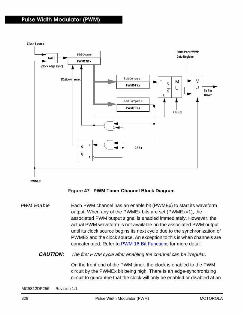
Pulse Width Modulator (PWM)
MC9S12DP256 — Revision 1.1
328 Pulse Width Modulator (PWM) MOTOROLA
Figure 47 PWM Timer Channel Block Diagram
PWM Enable Each PWM channel has an enable bit (PWMEx) to start its waveform output. When any of the PWMEx bits are set (PWMEx=1), the associated PWM output signal is enabled immediately. However, the actual PWM waveform is not available on the associated PWM output until its clock source begins its next cycle due to the synchronization of PWMEx and the clock source. An exception to this is when channels are concatenated. Refer to PWM 16-Bit Functions for more detail.
CAUTION: The first PWM cycle after enabling the channel can be irregular.
On the front end of the PWM timer, the clock is enabled to the PWM circuit by the PWMEx bit being high. There is an edge-synchronizing circuit to guarantee that the clock will only be enabled or disabled at an
Clock Source
T
R
Q
Q
MU
PPOLx
From Port PWMP
Data Register
PWMEx
(clock edge sync)
To PinDriver
GATE
8-bit Compare =
PWMDTYx
8-bit Compare =
PWMPERx
MU
CAEx
up/down
T
R
Q
Q
reset
8-bit Counter
PWMCNTx
Pulse Width Modulator (PWM)Functional Description
MC9S12DP256 — Revision 1.1
MOTOROLA Pulse Width Modulator (PWM) 329
edge. When the channel is disabled (PWMEx=0), the counter for the channel does not count.
PWM Polarity Each channel has a polarity bit to allow starting a waveform cycle with a high or low signal. This is shown on the block diagram as a mux select of either the Q output or the Q output of the PWM output flip flop. When one of the bits in the PWMPOL register is set, the associated PWM channel output is high at the beginning of the waveform, then goes low when the duty count is reached. Conversely, if the polarity bit is zero, the output starts low and then goes high when the duty count is reached.
PWM Period and Duty
Dedicated period and duty registers exist for each channel and are double buffered so that if they change while the channel is enabled, the change will NOT take effect until one of the following occurs:
• The effective period ends
• The counter is written (counter resets to $00)
• The channel is disabled
In this way, the output of the PWM will always be either the old waveform or the new waveform, not some variation in between. If the channel is not enabled, then writes to the period and duty registers will go directly to the latches as well as the buffer.
A change in duty or period can be forced into effect ‘immediately’ by writing the new value to the duty and/or period registers and then writing to the counter. This forces the counter to reset and the new duty and/or period values to be latched. In addition, since the counter is readable it is possible to know where the count is with respect to the duty value and software can be used to make adjustments
CAUTION: When forcing a new period or duty into effect immediately, an irregular PWM cycle can occur.
NOTE: Depending on the polarity bit, the duty registers will contain the count of either the high time or the low time.
Pulse Width Modulator (PWM)
MC9S12DP256 — Revision 1.1
330 Pulse Width Modulator (PWM) MOTOROLA
PWM Timer Counters
Each channel has a dedicated 8-bit up/down counter which runs at the rate of the selected clock source (reference PWM Clock Select for the available clock sources and rates). The counter compares to two registers, a duty register and a period register as shown in Figure 47. When the PWM counter matches the duty register the output flip-flop changes state causing the PWM waveform to also change state. A match between the PWM counter and the period register behaves differently depending on what output mode is selected as shown in Figure 47 and described in Left Aligned Outputs and Center Aligned Outputs.
Each channel counter can be read at anytime without affecting the count or the operation of the PWM channel.
Any value written to the counter causes the counter to reset to $00, the counter direction to be set to up, the immediate load of both duty and period registers with values from the buffers, and the output to change according to the polarity bit. When the channel is disabled (PWMEx=0), the counter stops. When a channel becomes enabled (PWMEx=1), the associated PWM counter continues from the count in the PWMCNTx register. This allows the waveform to continue where it left off when the channel is re-enabled. When the channel is disabled, writing ‘0’ to the period register will cause the counter to reset on the next selected clock.
NOTE: If the user wants to start a new ‘clean’ PWM waveform without any ‘history’ from the old waveform, the user must write to channel counter (PWMCNTx) prior to enabling the PWM channel (PWMEx=1).
Generally, writes to the counter are done prior to enabling a channel in order to start from a known state. However, writing a counter can also be done while the PWM channel is enabled (counting). The effect is similar to writing the counter when the channel is disabled except that the new period is started immediately with the output set according to the polarity bit.
CAUTION: Writing to the counter while the channel is enabled can cause an irregular PWM cycle to occur.

Pulse Width Modulator (PWM)Functional Description
MC9S12DP256 — Revision 1.1
MOTOROLA Pulse Width Modulator (PWM) 331
The counter is cleared at the end of the effective period (see Left Aligned Outputs and Center Aligned Outputs for more details).
Left Aligned Outputs
The PWM timer provides the choice of two types of outputs, Left Aligned or Center Aligned outputs. They are selected with the CAEx bits in the PWMCAE register. If the CAEx bit is cleared (CAEx=0), the corresponding PWM output will be left aligned.
In left aligned output mode, the 8-bit counter is configured as an up counter only. It compares to two registers, a duty register and a period register as shown in the block diagram in Figure 47. When the PWM counter matches the duty register the output flip-flop changes state causing the PWM waveform to also change state. A match between the PWM counter and the period register resets the counter and the output flip-flop as shown in Figure 47 as well as performing a load from the double buffer period and duty register to the associated registers as described in PWM Period and Duty. The counter counts from 0 to the value in the period register – 1.
NOTE: Changing the PWM output mode from Left Aligned Output to Center Aligned Output (or vice versa) while channels are operating can cause irregularities in the PWM output. It is recommended to program the output mode before enabling the PWM channel.
Table 52 PWM Timer Counter Conditions
Counter Clears ($00) Counter Counts Counter Stops
When PWMCNTx register written to any value
When PWM channel is enabled (PWMEx=1). Counts from last value in PWMCNTx.
When PWM channel is disabled (PWMEx=0)
Effective period ends
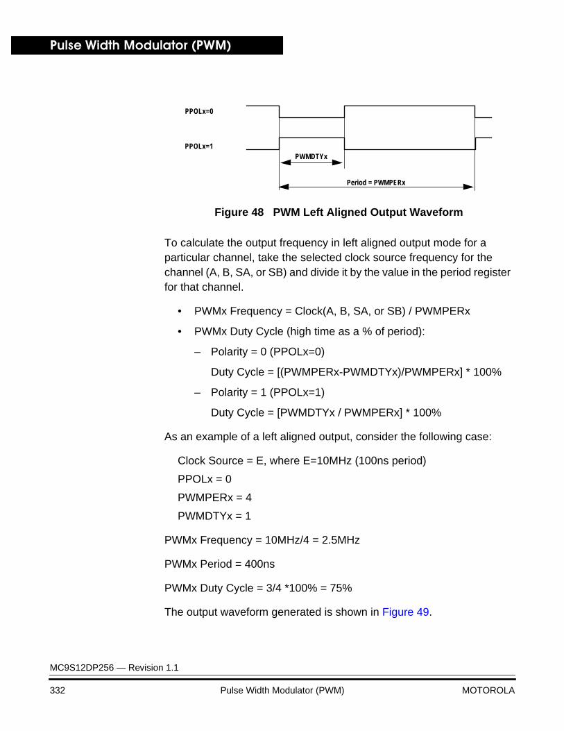
Pulse Width Modulator (PWM)
MC9S12DP256 — Revision 1.1
332 Pulse Width Modulator (PWM) MOTOROLA
Figure 48 PWM Left Aligned Output Waveform
To calculate the output frequency in left aligned output mode for a particular channel, take the selected clock source frequency for the channel (A, B, SA, or SB) and divide it by the value in the period register for that channel.
• PWMx Frequency = Clock(A, B, SA, or SB) / PWMPERx
• PWMx Duty Cycle (high time as a % of period):
– Polarity = 0 (PPOLx=0)
Duty Cycle = [(PWMPERx-PWMDTYx)/PWMPERx] * 100%
– Polarity = 1 (PPOLx=1)
Duty Cycle = [PWMDTYx / PWMPERx] * 100%
As an example of a left aligned output, consider the following case:
Clock Source = E, where E=10MHz (100ns period)
PPOLx = 0
PWMPERx = 4
PWMDTYx = 1
PWMx Frequency = 10MHz/4 = 2.5MHz
PWMx Period = 400ns
PWMx Duty Cycle = 3/4 *100% = 75%
The output waveform generated is shown in Figure 49.
PWMDTYx
Period = PWMPERx
PPOLx=0
PPOLx=1
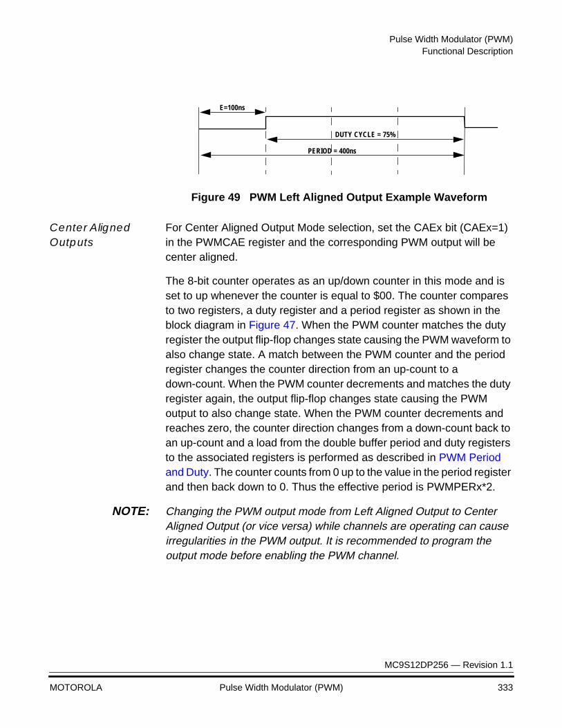
Pulse Width Modulator (PWM)Functional Description
MC9S12DP256 — Revision 1.1
MOTOROLA Pulse Width Modulator (PWM) 333
Figure 49 PWM Left Aligned Output Example Waveform
Center Aligned Outputs
For Center Aligned Output Mode selection, set the CAEx bit (CAEx=1) in the PWMCAE register and the corresponding PWM output will be center aligned.
The 8-bit counter operates as an up/down counter in this mode and is set to up whenever the counter is equal to $00. The counter compares to two registers, a duty register and a period register as shown in the block diagram in Figure 47. When the PWM counter matches the duty register the output flip-flop changes state causing the PWM waveform to also change state. A match between the PWM counter and the period register changes the counter direction from an up-count to a down-count. When the PWM counter decrements and matches the duty register again, the output flip-flop changes state causing the PWM output to also change state. When the PWM counter decrements and reaches zero, the counter direction changes from a down-count back to an up-count and a load from the double buffer period and duty registers to the associated registers is performed as described in PWM Period and Duty. The counter counts from 0 up to the value in the period register and then back down to 0. Thus the effective period is PWMPERx*2.
NOTE: Changing the PWM output mode from Left Aligned Output to Center Aligned Output (or vice versa) while channels are operating can cause irregularities in the PWM output. It is recommended to program the output mode before enabling the PWM channel.
PERIOD = 400ns
E=100ns
DUTY CYCLE = 75%
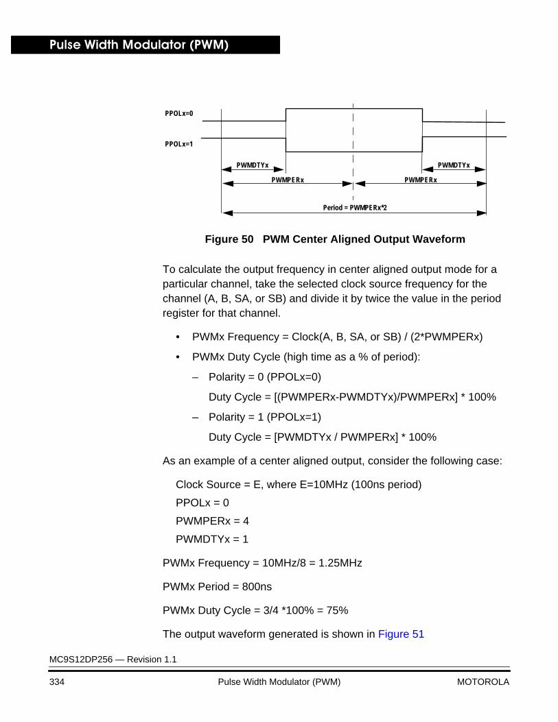
Pulse Width Modulator (PWM)
MC9S12DP256 — Revision 1.1
334 Pulse Width Modulator (PWM) MOTOROLA
Figure 50 PWM Center Aligned Output Waveform
To calculate the output frequency in center aligned output mode for a particular channel, take the selected clock source frequency for the channel (A, B, SA, or SB) and divide it by twice the value in the period register for that channel.
• PWMx Frequency = Clock(A, B, SA, or SB) / (2*PWMPERx)
• PWMx Duty Cycle (high time as a % of period):
– Polarity = 0 (PPOLx=0)
Duty Cycle = [(PWMPERx-PWMDTYx)/PWMPERx] * 100%
– Polarity = 1 (PPOLx=1)
Duty Cycle = [PWMDTYx / PWMPERx] * 100%
As an example of a center aligned output, consider the following case:
Clock Source = E, where E=10MHz (100ns period)
PPOLx = 0
PWMPERx = 4
PWMDTYx = 1
PWMx Frequency = 10MHz/8 = 1.25MHz
PWMx Period = 800ns
PWMx Duty Cycle = 3/4 *100% = 75%
The output waveform generated is shown in Figure 51
PPOLx=0
PPOLx=1
Period = PWMPERx*2
PWMDTYx PWMDTYx
PWMPERx PWMPERx
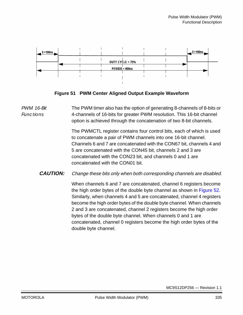
Pulse Width Modulator (PWM)Functional Description
MC9S12DP256 — Revision 1.1
MOTOROLA Pulse Width Modulator (PWM) 335
Figure 51 PWM Center Aligned Output Example Waveform
PWM 16-Bit Functions
The PWM timer also has the option of generating 8-channels of 8-bits or 4-channels of 16-bits for greater PWM resolution. This 16-bit channel option is achieved through the concatenation of two 8-bit channels.
The PWMCTL register contains four control bits, each of which is used to concatenate a pair of PWM channels into one 16-bit channel. Channels 6 and 7 are concatenated with the CON67 bit, channels 4 and 5 are concatenated with the CON45 bit, channels 2 and 3 are concatenated with the CON23 bit, and channels 0 and 1 are concatenated with the CON01 bit.
CAUTION: Change these bits only when both corresponding channels are disabled.
When channels 6 and 7 are concatenated, channel 6 registers become the high order bytes of the double byte channel as shown in Figure 52. Similarly, when channels 4 and 5 are concatenated, channel 4 registers become the high order bytes of the double byte channel. When channels 2 and 3 are concatenated, channel 2 registers become the high order bytes of the double byte channel. When channels 0 and 1 are concatenated, channel 0 registers become the high order bytes of the double byte channel.
PERIOD = 800ns
E=100ns
DUTY CYCLE = 75%
E=100ns
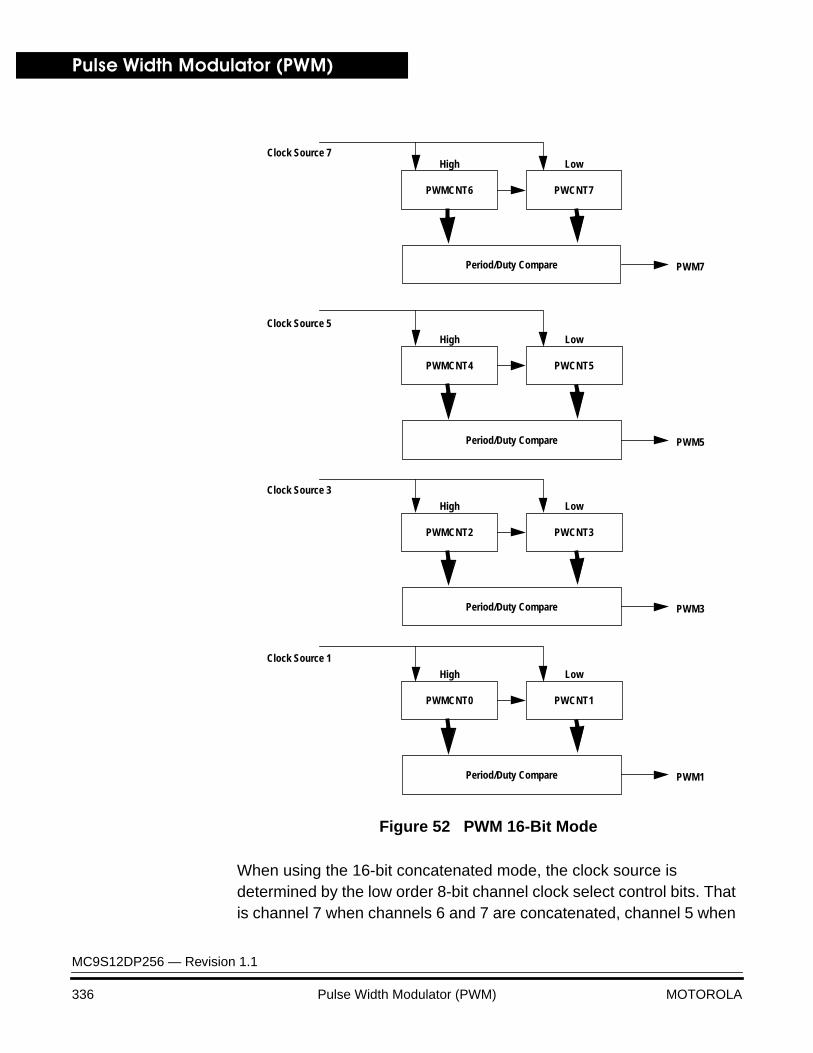
Pulse Width Modulator (PWM)
MC9S12DP256 — Revision 1.1
336 Pulse Width Modulator (PWM) MOTOROLA
Figure 52 PWM 16-Bit Mode
When using the 16-bit concatenated mode, the clock source is determined by the low order 8-bit channel clock select control bits. That is channel 7 when channels 6 and 7 are concatenated, channel 5 when
PWMCNT6 PWCNT7
PWM7
Clock Source 7High Low
Period/Duty Compare
PWMCNT4 PWCNT5
PWM5
Clock Source 5
High Low
Period/Duty Compare
PWMCNT2 PWCNT3
PWM3
Clock Source 3
High Low
Period/Duty Compare
PWMCNT0 PWCNT1
PWM1
Clock Source 1
High Low
Period/Duty Compare
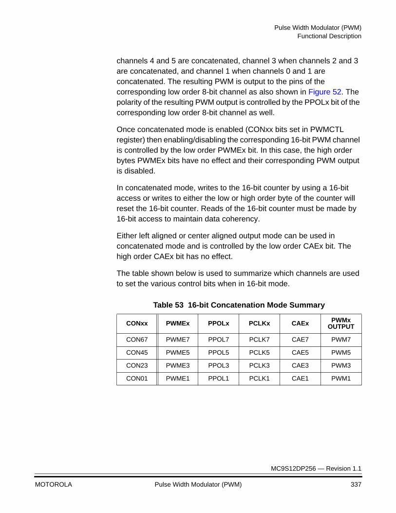
Pulse Width Modulator (PWM)Functional Description
MC9S12DP256 — Revision 1.1
MOTOROLA Pulse Width Modulator (PWM) 337
channels 4 and 5 are concatenated, channel 3 when channels 2 and 3 are concatenated, and channel 1 when channels 0 and 1 are concatenated. The resulting PWM is output to the pins of the corresponding low order 8-bit channel as also shown in Figure 52. The polarity of the resulting PWM output is controlled by the PPOLx bit of the corresponding low order 8-bit channel as well.
Once concatenated mode is enabled (CONxx bits set in PWMCTL register) then enabling/disabling the corresponding 16-bit PWM channel is controlled by the low order PWMEx bit. In this case, the high order bytes PWMEx bits have no effect and their corresponding PWM output is disabled.
In concatenated mode, writes to the 16-bit counter by using a 16-bit access or writes to either the low or high order byte of the counter will reset the 16-bit counter. Reads of the 16-bit counter must be made by 16-bit access to maintain data coherency.
Either left aligned or center aligned output mode can be used in concatenated mode and is controlled by the low order CAEx bit. The high order CAEx bit has no effect.
The table shown below is used to summarize which channels are used to set the various control bits when in 16-bit mode.
Table 53 16-bit Concatenation Mode Summary
CONxx PWMEx PPOLx PCLKx CAEx PWMx OUTPUT
CON67 PWME7 PPOL7 PCLK7 CAE7 PWM7
CON45 PWME5 PPOL5 PCLK5 CAE5 PWM5
CON23 PWME3 PPOL3 PCLK3 CAE3 PWM3
CON01 PWME1 PPOL1 PCLK1 CAE1 PWM1
Pulse Width Modulator (PWM)
MC9S12DP256 — Revision 1.1
338 Pulse Width Modulator (PWM) MOTOROLA
PWM Boundary Cases
The following table summarizes the boundary conditions for the PWM regardless of the output mode (Left Aligned or Center Aligned) and 8-bit (normal) or 16-bit (concatenation):
Reset Initialization
The reset state of each individual bit is listed within the Register Description section (see Register Descriptions) which details the registers and their bit-fields. All special functions or modes which are initialized during or just following reset are described within this section.
• The 8-bit up/down counter is configured as an up counter out of reset.
• All the channels are disabled and all the counters don’t count.
Table 54 PWM Boundary Cases
PWMDTYx PWMPERx PPOLx PWMx Output
$00 (indicates no duty)
>$00 1 Always Low
$00 (indicates no duty)
>$00 0 Always High
XX $00(1)
(indicates no period)
1. Counter=$00 and does not count.
1 Always High
XX $001
(indicates no period)0 Always Low
>= PWMPERx XX 1 Always High
>= PWMPERx XX 0 Always Low
Pulse Width Modulator (PWM)Modes of Operation
MC9S12DP256 — Revision 1.1
MOTOROLA Pulse Width Modulator (PWM) 339
Modes of Operation
Normal Modes The PWM module behaves as described within this specification in all normal modes.
Special Modes The PWM module behaves as described within this specification in all special modes.
WARNING: While in special modes, do not access registers $0006, $0007, $000A and $000B. Writing to any of these registers can alter the PWM functionality.
Emulation Modes In Freeze Mode, there is an option to disable the input clock to the prescaler by setting the PFRZ bit in the PWMCTL register. If this bit is set, whenever the MCU is in freeze mode the input clock to the prescaler is disabled. This feature is useful during emulation as it allows the PWM function to be suspended. In this way, the counters of the PWM can be stopped while in freeze mode so that once normal program flow is continued, the counters are re-enabled to simulate real-time operations. Since the registers can still be accessed in this mode, to re-enable the prescaler clock, either disable the PFRZ bit or exit freeze mode.
Security Modes The PWM module has no security features.

Pulse Width Modulator (PWM)
MC9S12DP256 — Revision 1.1
340 Pulse Width Modulator (PWM) MOTOROLA
Low Power Options
This section summarizes the low power options available in the PWM module. Low power design practices are implemented where possible.
The IP bus module clock (ipb_clk) is used for the programming model register writes. This clock is active only when module_en is asserted.
Run Mode While in run mode, if all eight PWM channels are disabled (PWME7–0=0), the prescaler counter shuts off for power savings (see Figure 46).
Wait Mode The PWM will keep running in WAIT unless the PSWAI bit in the PWMCTL register is enabled. This allows for lower power consumption in WAIT mode by disabling the input clock to the prescaler. When in WAIT mode with this bit set, no activity in the PWM occurs and the PWM outputs go to a static state (high or low).
Stop Mode In STOP mode, the PWM module is stopped since all the clocks from IP bus to the module are stopped. The PWM outputs go to a static state (high or low).
Interrupt Operation
The PWM module has only one interrupt which is generated at the time of emergency shutdown, if the corresponding enable bit (PWMIE in the PWMSDN register) is set.

MC9S12DP256 — Revision 1.1
MOTOROLA Enhanced Capture Timer (ECT) 341
Enhanced Capture Timer (ECT)Enhanced Capture Timer (ECT)
Contents
Overview . . . . . . . . . . . . . . . . . . . . . . . . . . . . . . . . . . . . . . . . . . . . . . 341Features . . . . . . . . . . . . . . . . . . . . . . . . . . . . . . . . . . . . . . . . . . . . . . 342Modes of Operation. . . . . . . . . . . . . . . . . . . . . . . . . . . . . . . . . . . . . . 342Abbreviations . . . . . . . . . . . . . . . . . . . . . . . . . . . . . . . . . . . . . . . . . . 342Block Diagram. . . . . . . . . . . . . . . . . . . . . . . . . . . . . . . . . . . . . . . . . . 344Signal Descriptions . . . . . . . . . . . . . . . . . . . . . . . . . . . . . . . . . . . . . . 350Module Memory Map . . . . . . . . . . . . . . . . . . . . . . . . . . . . . . . . . . . . 351Register Quick Reference . . . . . . . . . . . . . . . . . . . . . . . . . . . . . . . . . 354Register Descriptions . . . . . . . . . . . . . . . . . . . . . . . . . . . . . . . . . . . . 356Modes of Operation. . . . . . . . . . . . . . . . . . . . . . . . . . . . . . . . . . . . . . 383Interrupts . . . . . . . . . . . . . . . . . . . . . . . . . . . . . . . . . . . . . . . . . . . . . . 386Description of Interrupt Operation . . . . . . . . . . . . . . . . . . . . . . . . . . . 387
Overview
The HC12 Enhanced Capture Timer module has the features of the HC12 Standard Timer module enhanced by additional features in order to enlarge the field of applications, in particular for automotive ABS applications.
The basic timer consists of a 16-bit, software-programmable counter driven by a prescaler. This timer can be used for many purposes, including input waveform measurements while simultaneously generating an output waveform. Pulse widths can vary from microseconds to many seconds.
A full access for the counter registers or the input capture/output compare registers should take place in one clock cycle. Accessing high
Enhanced Capture Timer (ECT)
MC9S12DP256 — Revision 1.1
342 Enhanced Capture Timer (ECT) MOTOROLA
byte and low byte separately for all of these registers may not yield the same result as accessing them in one word.
Features
• 16-Bit Buffer Register for four Input Capture (IC) channels.
• Four 8-Bit Pulse Accumulators with 8-bit buffer registers associated with the four buffered IC channels. Configurable also as two 16-Bit Pulse Accumulators.
• 16-Bit Modulus Down-Counter with 4-bit Prescaler.
• Four user selectable Delay Counters for input noise immunity increase.
• Support for only 16-bit access on the IP bus.
Modes of Operation
STOP: Timer and modulus counter are off since clocks are stopped.
FREEZE: Timer and modulus counter keep on running, unless TSFRZ in TSCR($06) is set to one.
WAIT: Counters keep on running, unless TSWAI in TSCR ($06) is set to one.
NORMAL: Timer and modulus counter keep on running, unless TEN in TSCR($06) respectively MCEN in MCCTL ($26) are cleared.
Abbreviations
Following abbreviations are used in the document.
M clock – Module clock (clk of IPbus)

Enhanced Capture Timer (ECT)Abbreviations
MC9S12DP256 — Revision 1.1
MOTOROLA Enhanced Capture Timer (ECT) 343
PACLK – 16-bit pulse accumulator A (PACA) clock
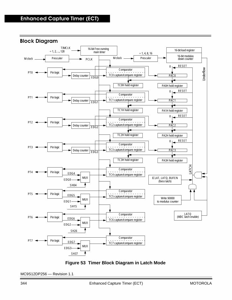
Enhanced Capture Timer (ECT)
MC9S12DP256 — Revision 1.1
344 Enhanced Capture Timer (ECT) MOTOROLA
Block Diagram
Figure 53 Timer Block Diagram in Latch Mode
16 Bit MAIN TIMER
PT1
Comparator
TC0H hold register
PT0
PT3
PT2
PT4
PT5
PT6
PT7
EDG0
EDG1
EDG2
EDG3
MUX
PrescalerM clock
16-bit load register
16-bit modulus
0 RESET
EDG0
EDG1
EDG2
EDG4
EDG5
EDG3
EDG6
EDG7
÷ 1, 4, 8, 16
16-bit Free-running
LATC
H
Und
erflo
w
main timer
Prescaler
TC0 capture/compare register
Comparator
TC1 capture/compare register
Comparator
TC2 capture/compare register
Comparator
TC3 capture/compare register
Comparator
TC4 capture/compare register
Comparator
TC5 capture/compare register
Comparator
TC6 capture/compare register
Comparator
TC7 capture/compare register
Pin logic
Pin logic
Pin logic
Pin logic
Pin logic
Pin logic
Pin logic
Pin logic
Delay counter
Delay counter
Delay counter
Delay counter
TC1H hold register
TC2H hold register
TC3H hold register
MUX
MUX
MUX
PA0H hold register
PAC0
0 RESET
PA1H hold register
PAC1
0 RESET
PA2H hold register
PAC2
0 RESET
PA3H hold register
PAC3
Write $0000to modulus counter
ICLAT, LATQ, BUFEN(force latch)
LATQ(MDC latch enable)
down counter
SH04
SH15
SH26
SH37
M clock
÷ 1, 2, ..., 128TIMCLK
PCLK
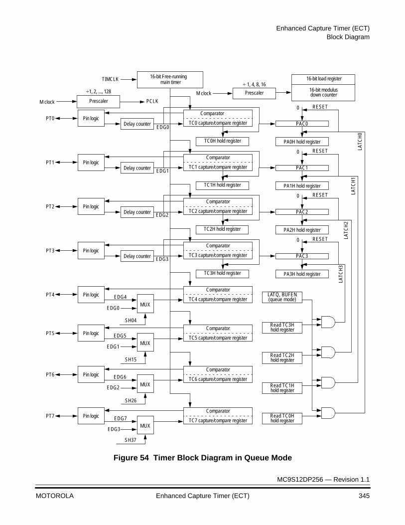
Enhanced Capture Timer (ECT)Block Diagram
MC9S12DP256 — Revision 1.1
MOTOROLA Enhanced Capture Timer (ECT) 345
Figure 54 Timer Block Diagram in Queue Mode
16 Bit MAIN TIMER
PT1
Comparator
TC0H hold register
PT0
PT3
PT2
PT4
PT5
PT6
PT7
EDG0
EDG1
EDG2
EDG3
MUX
PrescalerM clock
16-bit load register
16-bit modulus
0 RESET
EDG0
EDG1
EDG2
EDG4
EDG5
EDG3
EDG6
EDG7
÷1, 2, ..., 128÷ 1, 4, 8, 16
16-bit Free-running
LATC
H0
main timer
Prescaler
TC0 capture/compare register
Comparator
TC1 capture/compare register
Comparator
TC2 capture/compare register
Comparator
TC3 capture/compare register
Comparator
TC4 capture/compare register
Comparator
TC5 capture/compare register
Comparator
TC6 capture/compare register
Comparator
TC7 capture/compare register
Pin logic
Pin logic
Pin logic
Pin logic
Pin logic
Pin logic
Pin logic
Pin logic
Delay counter
Delay counter
Delay counter
Delay counter
M clock
TC1H hold register
TC2H hold register
TC3H hold register
MUX
MUX
MUX
PA0H hold register
PAC0
0 RESET
PA1H hold register
PAC1
0 RESET
PA2H hold register
PAC2
0 RESET
PA3H hold register
PAC3
LATC
H1
LATC
H3
LATC
H2
LATQ, BUFEN(queue mode)
Read TC3Hhold register
Read TC2Hhold register
Read TC1Hhold register
Read TC0Hhold register
down counter
SH04
SH15
SH26
SH37
PCLK
TIMCLK

Enhanced Capture Timer (ECT)
MC9S12DP256 — Revision 1.1
346 Enhanced Capture Timer (ECT) MOTOROLA
Figure 55 8-Bit Pulse Accumulators Block Diagram
IP d
ata
bus
PT0
Load holding register and reset pulse accumulator
0
0EDG3
EDG2
EDG1
EDG0Edge detector Delay counter
Interrupt
Interrupt
PT1 Edge detector Delay counter
PT2 Edge detector Delay counter
PT3 Edge detector Delay counter
8-bit PAC0 (PACN0)
PA0H holding register
0
8-bit PAC1 (PACN1)
PA1H holding register
0
8-bit PAC2 (PACN2)
PA2H holding register
0
8-bit PAC3 (PACN3)
PA3H holding register
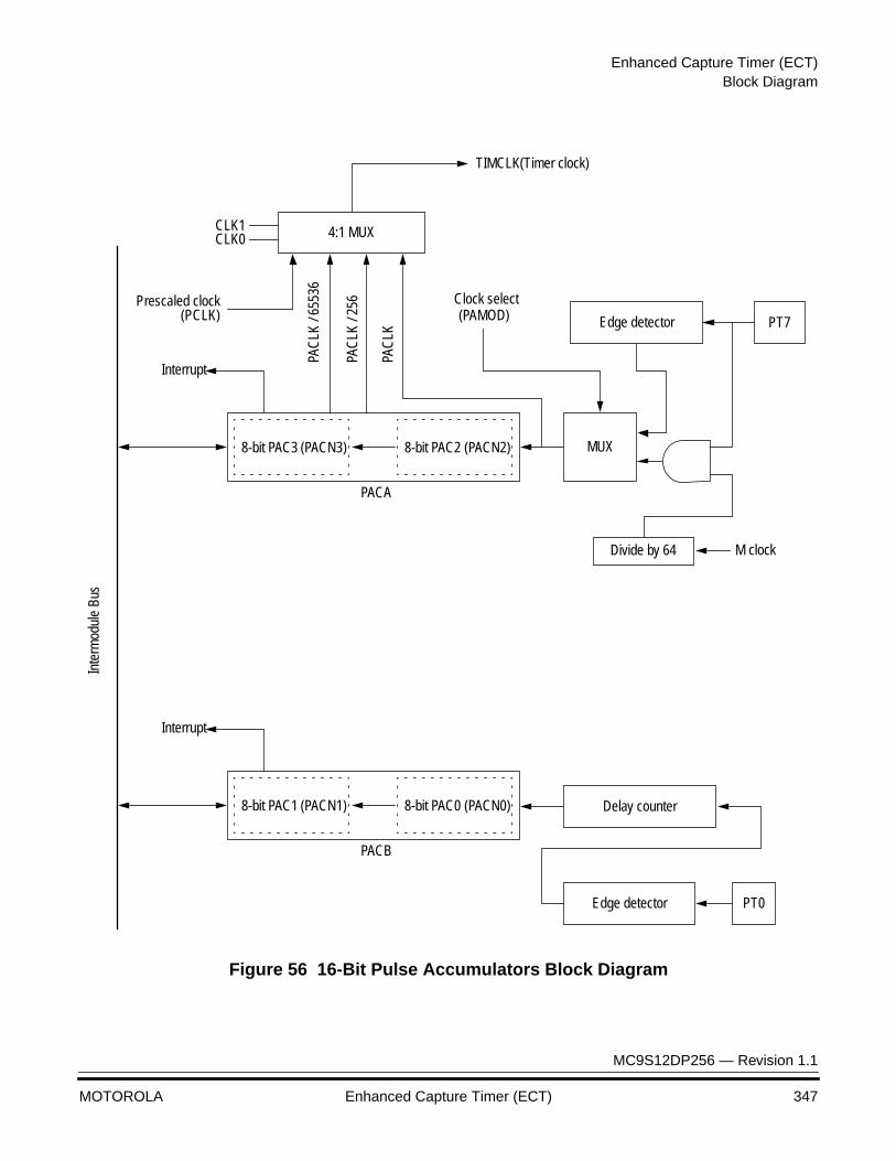
Enhanced Capture Timer (ECT)Block Diagram
MC9S12DP256 — Revision 1.1
MOTOROLA Enhanced Capture Timer (ECT) 347
Figure 56 16-Bit Pulse Accumulators Block Diagram
Edge detector
8-bit PAC2
Inte
rmod
ule
Bus
8-bit PAC3
PT7
PT0
M clockDivide by 64
Clock select
CLK0CLK1 4:1 MUX
TIMCLK
PAC
LK
PAC
LK /
256
PAC
LK /
6553
6Prescaled clock
(PCLK)
(Timer clock)
Interrupt
MUX
(PAMOD)
Edge detector
PACA
Delay counter
(PACN3) (PACN2)
8-bit PAC08-bit PAC1
Interrupt
PACB
(PACN1) (PACN0)
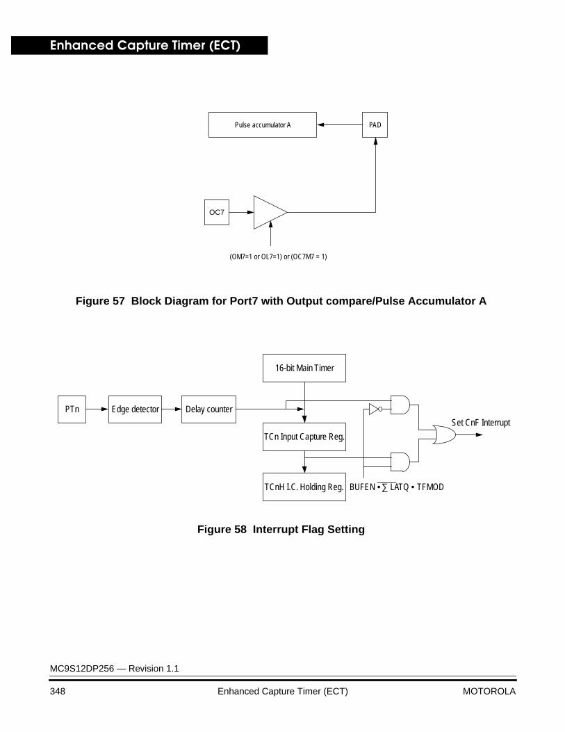
Enhanced Capture Timer (ECT)
MC9S12DP256 — Revision 1.1
348 Enhanced Capture Timer (ECT) MOTOROLA
Figure 57 Block Diagram for Port7 with Output compare/Pulse Accumulator A
Figure 58 Interrupt Flag Setting
Pulse accumulator A PAD
(OM7=1 or OL7=1) or (OC7M7 = 1)
OC7
PTn Edge detector Delay counter
16-bit Main Timer
TCn Input Capture Reg.
TCnH I.C. Holding Reg. BUFEN •∑ LATQ • TFMOD
Set CnF Interrupt
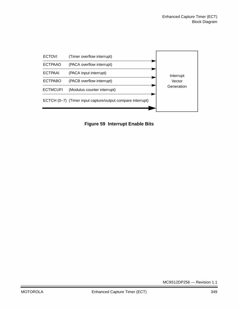
Enhanced Capture Timer (ECT)Block Diagram
MC9S12DP256 — Revision 1.1
MOTOROLA Enhanced Capture Timer (ECT) 349
Figure 59 Interrupt Enable Bits
ECTOVI
ECTPABOInterrupt
GenerationVector
ECTCH (0–7)
ECTMCUFI
ECTPAAO
ECTPAAI
(Timer overflow interrupt)
(PACA overflow interrupt)
(PACA input interrupt)
(PACB overflow interrupt)
(Modulus counter interrupt)
(Timer input capture/output compare interrupt)
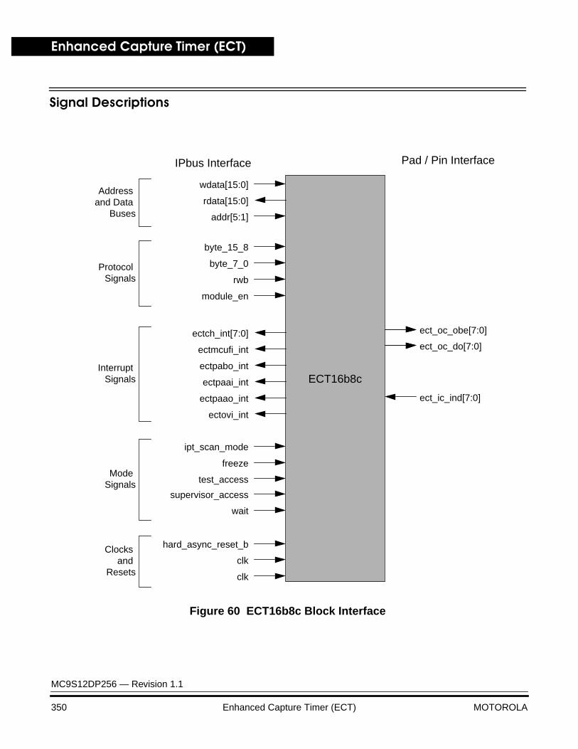
Enhanced Capture Timer (ECT)
MC9S12DP256 — Revision 1.1
350 Enhanced Capture Timer (ECT) MOTOROLA
Signal Descriptions
Figure 60 ECT16b8c Block Interface
ECT16b8c
wdata[15:0]
rdata[15:0]
addr[5:1]
byte_15_8
byte_7_0
rwb
ectmcufi_int
test_access
clk
IPbus Interface Pad / Pin Interface
ectpabo_int
ectpaai_int
ectpaao_int
ectovi_int
hard_async_reset_b
supervisor_access
ectch_int[7:0]
wait
ect_oc_obe[7:0]
ect_oc_do[7:0]
ect_ic_ind[7:0]
freeze
ipt_scan_mode
module_en
clk
Address and Data
Buses
Protocol Signals
Interrupt Signals
Mode Signals
Clocks and
Resets
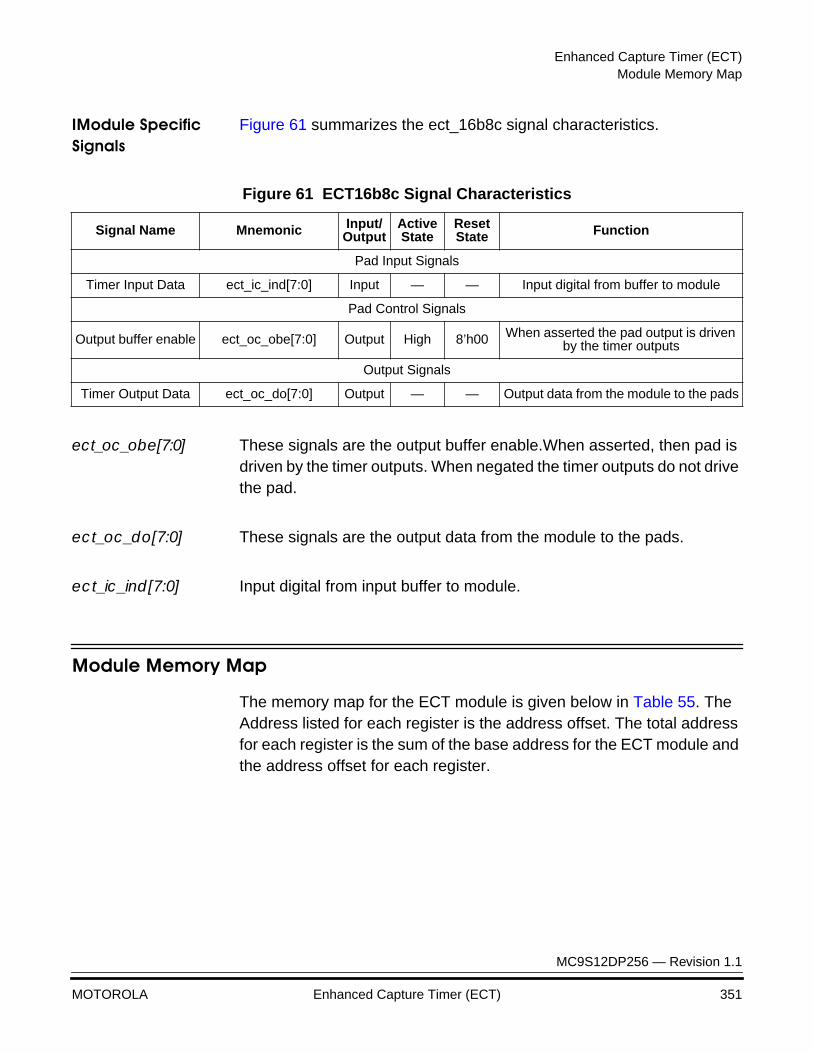
Enhanced Capture Timer (ECT)Module Memory Map
MC9S12DP256 — Revision 1.1
MOTOROLA Enhanced Capture Timer (ECT) 351
IModule Specific Signals
Figure 61 summarizes the ect_16b8c signal characteristics.
ect_oc_obe[7:0] These signals are the output buffer enable.When asserted, then pad is driven by the timer outputs. When negated the timer outputs do not drive the pad.
ect_oc_do[7:0] These signals are the output data from the module to the pads.
ect_ic_ind[7:0] Input digital from input buffer to module.
Module Memory Map
The memory map for the ECT module is given below in Table 55. The Address listed for each register is the address offset. The total address for each register is the sum of the base address for the ECT module and the address offset for each register.
Figure 61 ECT16b8c Signal Characteristics
Signal Name Mnemonic Input/Output
ActiveState
ResetState Function
Pad Input Signals
Timer Input Data ect_ic_ind[7:0] Input — — Input digital from buffer to module
Pad Control Signals
Output buffer enable ect_oc_obe[7:0] Output High 8’h00 When asserted the pad output is driven by the timer outputs
Output Signals
Timer Output Data ect_oc_do[7:0] Output — — Output data from the module to the pads
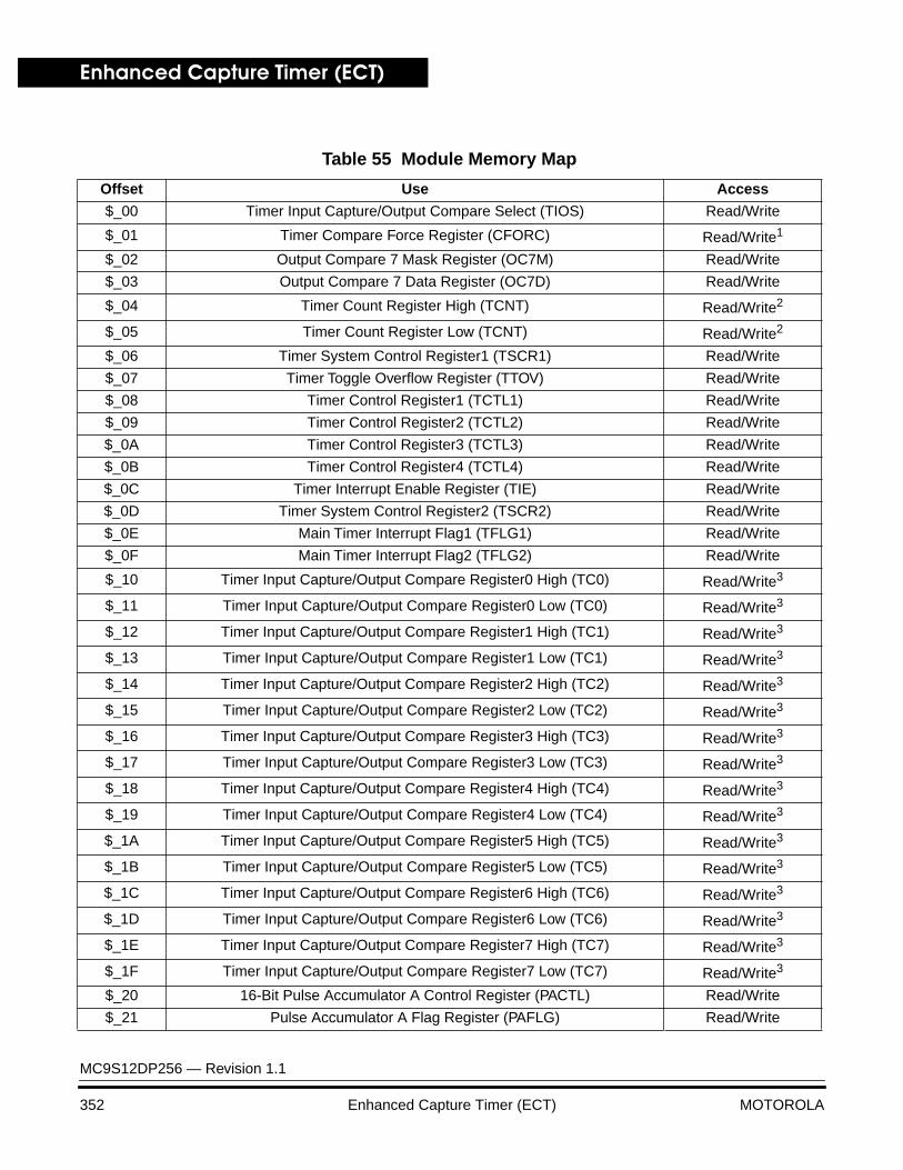
Enhanced Capture Timer (ECT)
MC9S12DP256 — Revision 1.1
352 Enhanced Capture Timer (ECT) MOTOROLA
Table 55 Module Memory Map
Offset Use Access
$_00 Timer Input Capture/Output Compare Select (TIOS) Read/Write
$_01 Timer Compare Force Register (CFORC) Read/Write1
$_02 Output Compare 7 Mask Register (OC7M) Read/Write
$_03 Output Compare 7 Data Register (OC7D) Read/Write
$_04 Timer Count Register High (TCNT) Read/Write2
$_05 Timer Count Register Low (TCNT) Read/Write2
$_06 Timer System Control Register1 (TSCR1) Read/Write
$_07 Timer Toggle Overflow Register (TTOV) Read/Write
$_08 Timer Control Register1 (TCTL1) Read/Write
$_09 Timer Control Register2 (TCTL2) Read/Write
$_0A Timer Control Register3 (TCTL3) Read/Write
$_0B Timer Control Register4 (TCTL4) Read/Write
$_0C Timer Interrupt Enable Register (TIE) Read/Write
$_0D Timer System Control Register2 (TSCR2) Read/Write
$_0E Main Timer Interrupt Flag1 (TFLG1) Read/Write
$_0F Main Timer Interrupt Flag2 (TFLG2) Read/Write
$_10 Timer Input Capture/Output Compare Register0 High (TC0) Read/Write3
$_11 Timer Input Capture/Output Compare Register0 Low (TC0) Read/Write3
$_12 Timer Input Capture/Output Compare Register1 High (TC1) Read/Write3
$_13 Timer Input Capture/Output Compare Register1 Low (TC1) Read/Write3
$_14 Timer Input Capture/Output Compare Register2 High (TC2) Read/Write3
$_15 Timer Input Capture/Output Compare Register2 Low (TC2) Read/Write3
$_16 Timer Input Capture/Output Compare Register3 High (TC3) Read/Write3
$_17 Timer Input Capture/Output Compare Register3 Low (TC3) Read/Write3
$_18 Timer Input Capture/Output Compare Register4 High (TC4) Read/Write3
$_19 Timer Input Capture/Output Compare Register4 Low (TC4) Read/Write3
$_1A Timer Input Capture/Output Compare Register5 High (TC5) Read/Write3
$_1B Timer Input Capture/Output Compare Register5 Low (TC5) Read/Write3
$_1C Timer Input Capture/Output Compare Register6 High (TC6) Read/Write3
$_1D Timer Input Capture/Output Compare Register6 Low (TC6) Read/Write3
$_1E Timer Input Capture/Output Compare Register7 High (TC7) Read/Write3
$_1F Timer Input Capture/Output Compare Register7 Low (TC7) Read/Write3
$_20 16-Bit Pulse Accumulator A Control Register (PACTL) Read/Write
$_21 Pulse Accumulator A Flag Register (PAFLG) Read/Write
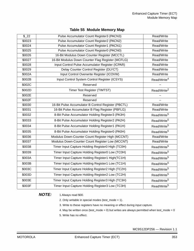
Enhanced Capture Timer (ECT)Module Memory Map
MC9S12DP256 — Revision 1.1
MOTOROLA Enhanced Capture Timer (ECT) 353
NOTE: 1.Always read $00.
2. Only writable in special modes (test_mode = 1).
3. Write to these registers have no meaning or effect during input capture.
4. May be written once (test_mode = 0) but writes are always permitted when test_mode = 0
5. Write has no effect.
$_22 Pulse Accumulator Count Register3 (PACN3) Read/Write
$0023 Pulse Accumulator Count Register2 (PACN2) Read/Write
$0024 Pulse Accumulator Count Register1 (PACN1) Read/Write
$0025 Pulse Accumulator Count Register0 (PACN0) Read/Write
$0026 16-Bit Modulus Down Counter Register (MCCTL) Read/Write
$0027 16-Bit Modulus Down Counter Flag Register (MCFLG) Read/Write
$0028 Input Control Pulse Accumulator Register (ICPAR) Read/Write
$0029 Delay Counter Control Register (DLYCT) Read/Write
$002A Input Control Overwrite Register (ICOVW) Read/Write
$002B Input Control System Control Register (ICSYS) Read/Write4
$002C Reserved –
$002D Timer Test Register (TIMTST) Read/Write2
$002E Reserved –
$002F Reserved –
$0030 16-Bit Pulse Accumulator B Control Register (PBCTL) Read/Write
$0031 16-Bit Pulse Accumulator B Flag Register (PBFLG) Read/Write
$0032 8-Bit Pulse Accumulator Holding Register3 (PA3H) Read/Write5
$0033 8-Bit Pulse Accumulator Holding Register2 (PA2H) Read/Write5
$0034 8-Bit Pulse Accumulator Holding Register1 (PA1H) Read/Write5
$0035 8-Bit Pulse Accumulator Holding Register0 (PA0H) Read/Write5
$0036 Modulus Down-Counter Count Register High (MCCNT) Read/Write
$0037 Modulus Down-Counter Count Register Low (MCCNT) Read/Write
$0038 Timer Input Capture Holding Register0 High (TC0H) Read/Write5
$0039 Timer Input Capture Holding Register0 Low (TC0H) Read/Write5
$003A Timer Input Capture Holding Register1 High(TC1H) Read/Write5
$003B Timer Input Capture Holding Register1 Low (TC1H) Read/Write5
$003C Timer Input Capture Holding Register2 High (TC2H) Read/Write5
$003D Timer Input Capture Holding Register2 Low (TC2H) Read/Write5
$003E Timer Input Capture Holding Register3 High (TC3H) Read/Write5
$003F Timer Input Capture Holding Register3 Low (TC3H) Read/Write5
Table 55 Module Memory Map
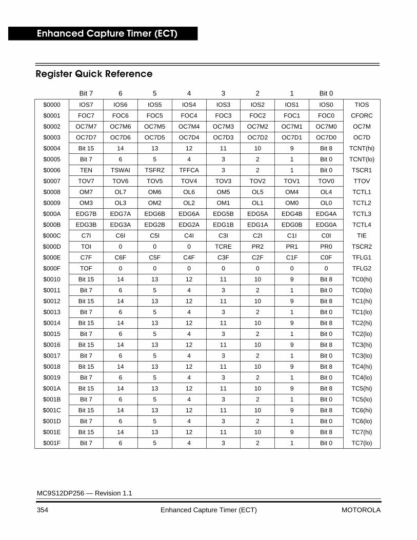
Enhanced Capture Timer (ECT)
MC9S12DP256 — Revision 1.1
354 Enhanced Capture Timer (ECT) MOTOROLA
Register Quick Reference
Bit 7 6 5 4 3 2 1 Bit 0
$0000 IOS7 IOS6 IOS5 IOS4 IOS3 IOS2 IOS1 IOS0 TIOS
$0001 FOC7 FOC6 FOC5 FOC4 FOC3 FOC2 FOC1 FOC0 CFORC
$0002 OC7M7 OC7M6 OC7M5 OC7M4 OC7M3 OC7M2 OC7M1 OC7M0 OC7M
$0003 OC7D7 OC7D6 OC7D5 OC7D4 OC7D3 OC7D2 OC7D1 OC7D0 OC7D
$0004 Bit 15 14 13 12 11 10 9 Bit 8 TCNT(hi)
$0005 Bit 7 6 5 4 3 2 1 Bit 0 TCNT(lo)
$0006 TEN TSWAI TSFRZ TFFCA 3 2 1 Bit 0 TSCR1
$0007 TOV7 TOV6 TOV5 TOV4 TOV3 TOV2 TOV1 TOV0 TTOV
$0008 OM7 OL7 OM6 OL6 OM5 OL5 OM4 OL4 TCTL1
$0009 OM3 OL3 OM2 OL2 OM1 OL1 OM0 OL0 TCTL2
$000A EDG7B EDG7A EDG6B EDG6A EDG5B EDG5A EDG4B EDG4A TCTL3
$000B EDG3B EDG3A EDG2B EDG2A EDG1B EDG1A EDG0B EDG0A TCTL4
$000C C7I C6I C5I C4I C3I C2I C1I C0I TIE
$000D TOI 0 0 0 TCRE PR2 PR1 PR0 TSCR2
$000E C7F C6F C5F C4F C3F C2F C1F C0F TFLG1
$000F TOF 0 0 0 0 0 0 0 TFLG2
$0010 Bit 15 14 13 12 11 10 9 Bit 8 TC0(hi)
$0011 Bit 7 6 5 4 3 2 1 Bit 0 TC0(lo)
$0012 Bit 15 14 13 12 11 10 9 Bit 8 TC1(hi)
$0013 Bit 7 6 5 4 3 2 1 Bit 0 TC1(lo)
$0014 Bit 15 14 13 12 11 10 9 Bit 8 TC2(hi)
$0015 Bit 7 6 5 4 3 2 1 Bit 0 TC2(lo)
$0016 Bit 15 14 13 12 11 10 9 Bit 8 TC3(hi)
$0017 Bit 7 6 5 4 3 2 1 Bit 0 TC3(lo)
$0018 Bit 15 14 13 12 11 10 9 Bit 8 TC4(hi)
$0019 Bit 7 6 5 4 3 2 1 Bit 0 TC4(lo)
$001A Bit 15 14 13 12 11 10 9 Bit 8 TC5(hi)
$001B Bit 7 6 5 4 3 2 1 Bit 0 TC5(lo)
$001C Bit 15 14 13 12 11 10 9 Bit 8 TC6(hi)
$001D Bit 7 6 5 4 3 2 1 Bit 0 TC6(lo)
$001E Bit 15 14 13 12 11 10 9 Bit 8 TC7(hi)
$001F Bit 7 6 5 4 3 2 1 Bit 0 TC7(lo)
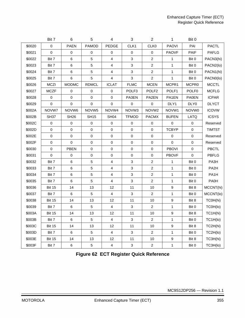
Enhanced Capture Timer (ECT)Register Quick Reference
MC9S12DP256 — Revision 1.1
MOTOROLA Enhanced Capture Timer (ECT) 355
Figure 62 ECT Register Quick Reference
$0020 0 PAEN PAMOD PEDGE CLK1 CLK0 PAOVI PAI PACTL
$0021 0 0 0 0 0 0 PAOVF PAIF PAFLG
$0022 Bit 7 6 5 4 3 2 1 Bit 0 PACN3(hi)
$0023 Bit 7 6 5 4 3 2 1 Bit 0 PACN2(lo)
$0024 Bit 7 6 5 4 3 2 1 Bit 0 PACN1(hi)
$0025 Bit 7 6 5 4 3 2 1 Bit 0 PACN0(lo)
$0026 MCZI MODMC RDMCL ICLAT FLMC MCEN MCPR1 MCPR0 MCCTL
$0027 MCZF 0 0 0 POLF3 POLF2 POLF1 POLF0 MCFLG
$0028 0 0 0 0 PA3EN PA2EN PA1EN PA0EN ICPAR
$0029 0 0 0 0 0 0 DLY1 DLY0 DLYCT
$002A NOVW7 NOVW6 NOVW5 NOVW4 NOVW3 NOVW2 NOVW1 NOVW0 ICOVW
$002B SH37 SH26 SH15 SH04 TFMOD PACMX BUFEN LATQ ICSYS
$002C 0 0 0 0 0 0 0 0 Reserved
$002D 0 0 0 0 0 0 TCBYP 0 TIMTST
$002E 0 0 0 0 0 0 0 0 Reserved
$002F 0 0 0 0 0 0 0 0 Reserved
$0030 0 PBEN 0 0 0 0 PBOVI 0 PBCTL
$0031 0 0 0 0 0 0 PBOVF 0 PBFLG
$0032 Bit 7 6 5 4 3 2 1 Bit 0 PA3H
$0033 Bit 7 6 5 4 3 2 1 Bit 0 PA2H
$0034 Bit 7 6 5 4 3 2 1 Bit 0 PA1H
$0035 Bit 7 6 5 4 3 2 1 Bit 0 PA0H
$0036 Bit 15 14 13 12 11 10 9 Bit 8 MCCNT(hi)
$0037 Bit 7 6 5 4 3 2 1 Bit 0 MCCNT(lo)
$0038 Bit 15 14 13 12 11 10 9 Bit 8 TC0H(hi)
$0039 Bit 7 6 5 4 3 2 1 Bit 0 TC0H(lo)
$003A Bit 15 14 13 12 11 10 9 Bit 8 TC1H(hi)
$003B Bit 7 6 5 4 3 2 1 Bit 0 TC1H(lo)
$003C Bit 15 14 13 12 11 10 9 Bit 8 TC2H(hi)
$003D Bit 7 6 5 4 3 2 1 Bit 0 TC2H(lo)
$003E Bit 15 14 13 12 11 10 9 Bit 8 TC3H(hi)
$003F Bit 7 6 5 4 3 2 1 Bit 0 TC3H(lo)
Bit 7 6 5 4 3 2 1 Bit 0
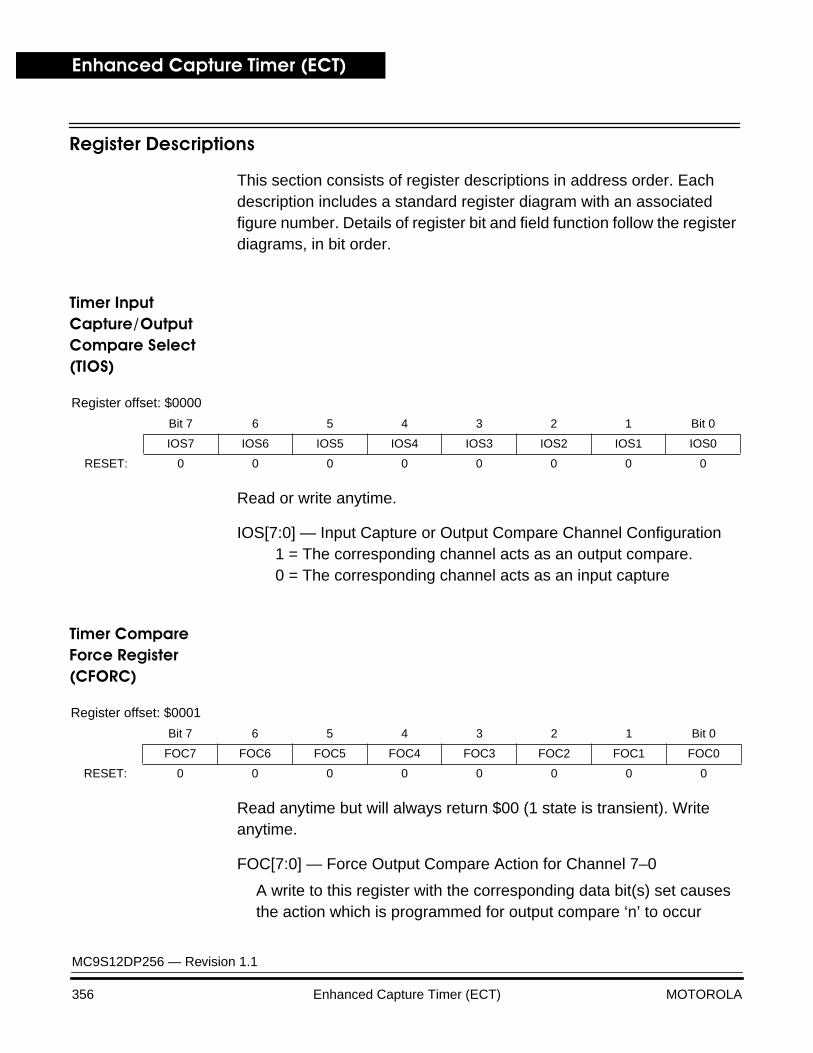
Enhanced Capture Timer (ECT)
MC9S12DP256 — Revision 1.1
356 Enhanced Capture Timer (ECT) MOTOROLA
Register Descriptions
This section consists of register descriptions in address order. Each description includes a standard register diagram with an associated figure number. Details of register bit and field function follow the register diagrams, in bit order.
Timer Input Capture/Output Compare Select (TIOS)
Read or write anytime.
IOS[7:0] — Input Capture or Output Compare Channel Configuration1 = The corresponding channel acts as an output compare.0 = The corresponding channel acts as an input capture
Timer Compare Force Register (CFORC)
Read anytime but will always return $00 (1 state is transient). Write anytime.
FOC[7:0] — Force Output Compare Action for Channel 7–0
A write to this register with the corresponding data bit(s) set causes the action which is programmed for output compare ‘n’ to occur
Register offset: $0000
Bit 7 6 5 4 3 2 1 Bit 0
IOS7 IOS6 IOS5 IOS4 IOS3 IOS2 IOS1 IOS0
RESET: 0 0 0 0 0 0 0 0
Register offset: $0001
Bit 7 6 5 4 3 2 1 Bit 0
FOC7 FOC6 FOC5 FOC4 FOC3 FOC2 FOC1 FOC0
RESET: 0 0 0 0 0 0 0 0
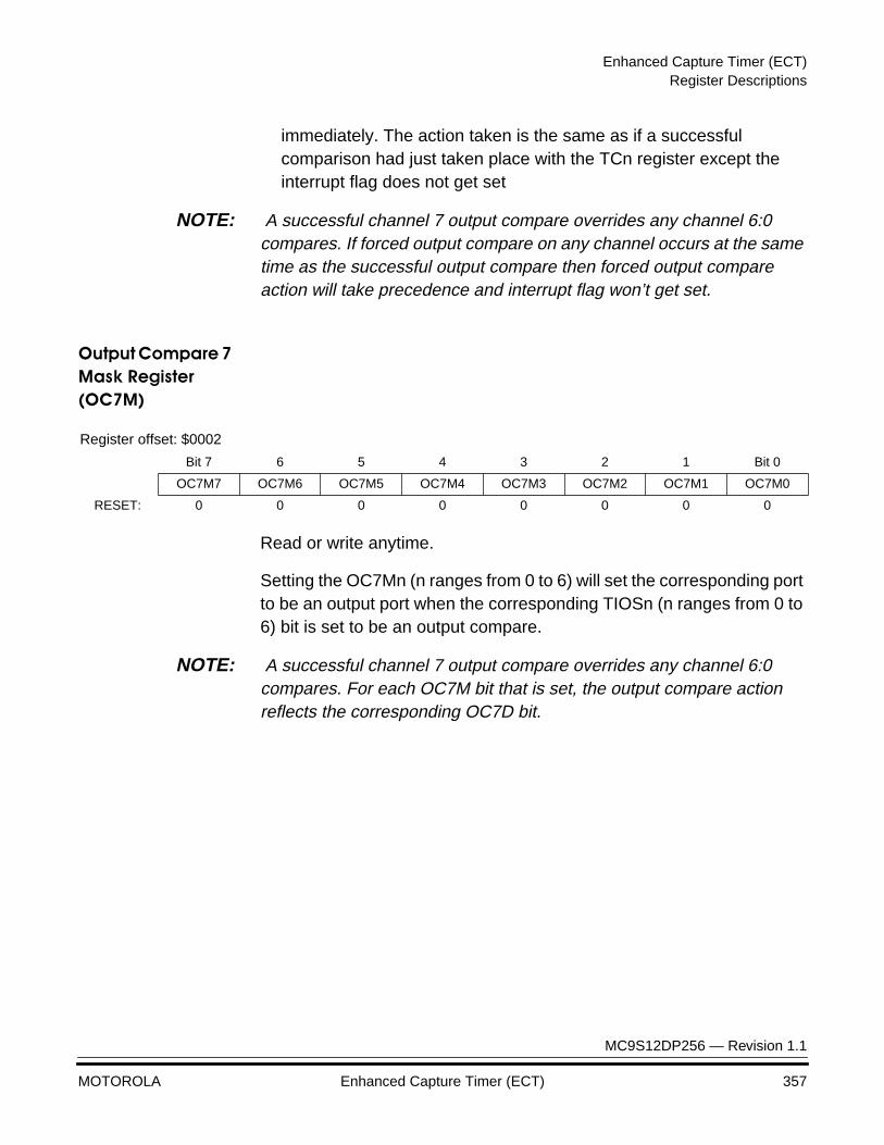
Enhanced Capture Timer (ECT)Register Descriptions
MC9S12DP256 — Revision 1.1
MOTOROLA Enhanced Capture Timer (ECT) 357
immediately. The action taken is the same as if a successful comparison had just taken place with the TCn register except the interrupt flag does not get set
NOTE: A successful channel 7 output compare overrides any channel 6:0 compares. If forced output compare on any channel occurs at the same time as the successful output compare then forced output compare action will take precedence and interrupt flag won’t get set.
Output Compare 7 Mask Register (OC7M)
Read or write anytime.
Setting the OC7Mn (n ranges from 0 to 6) will set the corresponding port to be an output port when the corresponding TIOSn (n ranges from 0 to 6) bit is set to be an output compare.
NOTE: A successful channel 7 output compare overrides any channel 6:0 compares. For each OC7M bit that is set, the output compare action reflects the corresponding OC7D bit.
Register offset: $0002
Bit 7 6 5 4 3 2 1 Bit 0
OC7M7 OC7M6 OC7M5 OC7M4 OC7M3 OC7M2 OC7M1 OC7M0
RESET: 0 0 0 0 0 0 0 0
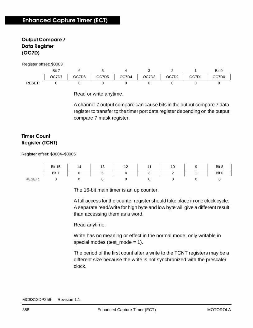
Enhanced Capture Timer (ECT)
MC9S12DP256 — Revision 1.1
358 Enhanced Capture Timer (ECT) MOTOROLA
Output Compare 7 Data Register (OC7D)
Read or write anytime.
A channel 7 output compare can cause bits in the output compare 7 data register to transfer to the timer port data register depending on the output compare 7 mask register.
Timer Count Register (TCNT)
The 16-bit main timer is an up counter.
A full access for the counter register should take place in one clock cycle. A separate read/write for high byte and low byte will give a different result than accessing them as a word.
Read anytime.
Write has no meaning or effect in the normal mode; only writable in special modes (test_mode = 1).
The period of the first count after a write to the TCNT registers may be a different size because the write is not synchronized with the prescaler clock.
Register offset: $0003
Bit 7 6 5 4 3 2 1 Bit 0
OC7D7 OC7D6 OC7D5 OC7D4 OC7D3 OC7D2 OC7D1 OC7D0
RESET: 0 0 0 0 0 0 0 0
Register offset: $0004–$0005
Bit 15 14 13 12 11 10 9 Bit 8
Bit 7 6 5 4 3 2 1 Bit 0
RESET: 0 0 0 0 0 0 0 0
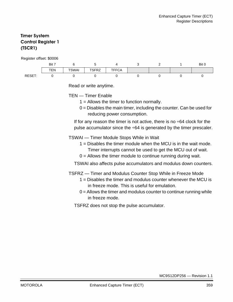
Enhanced Capture Timer (ECT)Register Descriptions
MC9S12DP256 — Revision 1.1
MOTOROLA Enhanced Capture Timer (ECT) 359
Timer System Control Register 1 (TSCR1)
Read or write anytime.
TEN — Timer Enable1 = Allows the timer to function normally.0 = Disables the main timer, including the counter. Can be used for
reducing power consumption.
If for any reason the timer is not active, there is no ÷64 clock for the pulse accumulator since the ÷64 is generated by the timer prescaler.
TSWAI — Timer Module Stops While in Wait1 = Disables the timer module when the MCU is in the wait mode.
Timer interrupts cannot be used to get the MCU out of wait.0 = Allows the timer module to continue running during wait.
TSWAI also affects pulse accumulators and modulus down counters.
TSFRZ — Timer and Modulus Counter Stop While in Freeze Mode1 = Disables the timer and modulus counter whenever the MCU is
in freeze mode. This is useful for emulation.0 = Allows the timer and modulus counter to continue running while
in freeze mode.
TSFRZ does not stop the pulse accumulator.
Register offset: $0006
Bit 7 6 5 4 3 2 1 Bit 0
TEN TSWAI TSFRZ TFFCA
RESET: 0 0 0 0 0 0 0 0
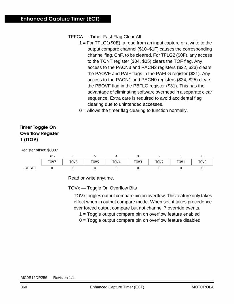
Enhanced Capture Timer (ECT)
MC9S12DP256 — Revision 1.1
360 Enhanced Capture Timer (ECT) MOTOROLA
TFFCA — Timer Fast Flag Clear All 1 = For TFLG1($0E), a read from an input capture or a write to the
output compare channel ($10–$1F) causes the corresponding channel flag, CnF, to be cleared. For TFLG2 ($0F), any access to the TCNT register ($04, $05) clears the TOF flag. Any access to the PACN3 and PACN2 registers ($22, $23) clears the PAOVF and PAIF flags in the PAFLG register ($21). Any access to the PACN1 and PACN0 registers ($24, $25) clears the PBOVF flag in the PBFLG register ($31). This has the advantage of eliminating software overhead in a separate clear sequence. Extra care is required to avoid accidental flag clearing due to unintended accesses.
0 = Allows the timer flag clearing to function normally.
Timer Toggle On Overflow Register 1 (TTOV)
Read or write anytime.
TOVx — Toggle On Overflow Bits
TOVx toggles output compare pin on overflow. This feature only takes effect when in output compare mode. When set, it takes precedence over forced output compare but not channel 7 override events.
1 = Toggle output compare pin on overflow feature enabled0 = Toggle output compare pin on overflow feature disabled
Register offset: $0007
Bit 7 6 5 4 3 2 1 0
TOV7 TOV6 TOV5 TOV4 TOV3 TOV2 TOV1 TOV0
RESET 0 0 0 0 0 0 0 0
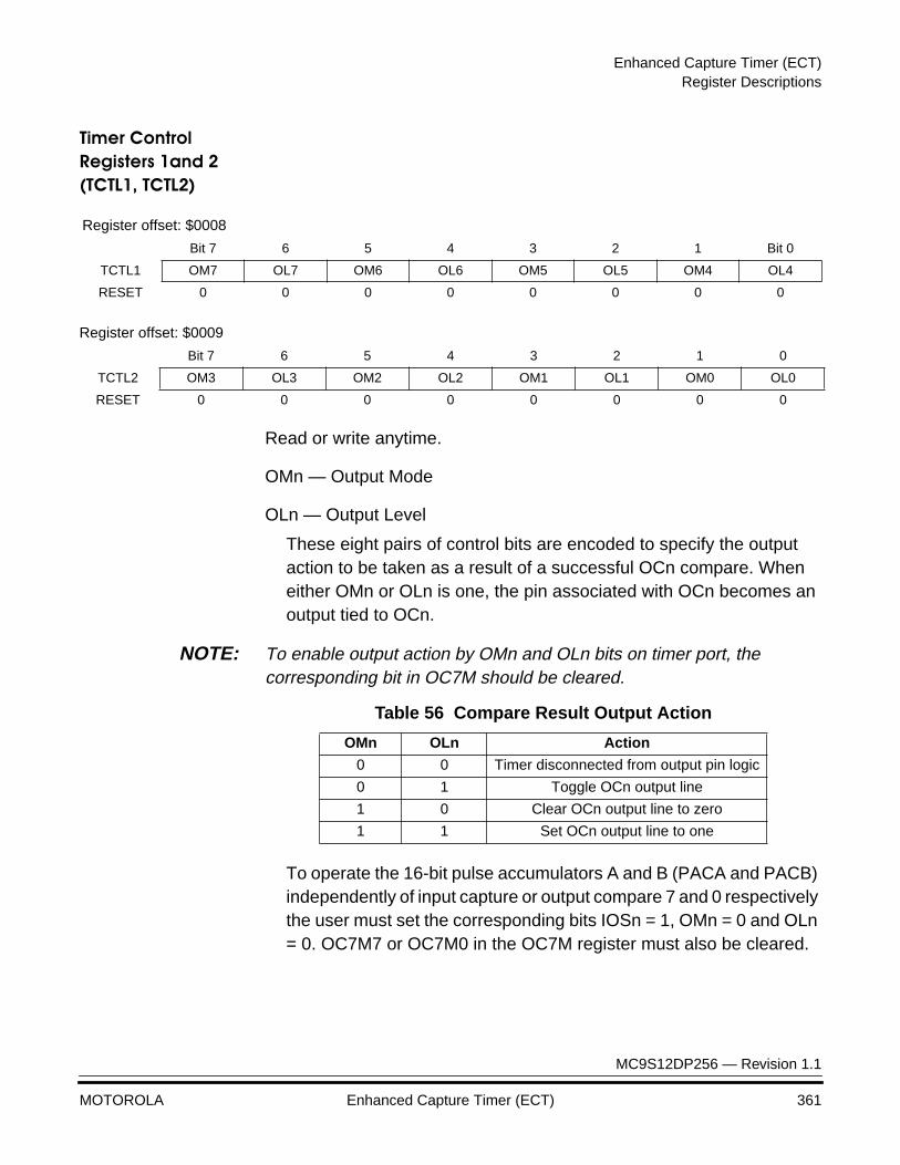
Enhanced Capture Timer (ECT)Register Descriptions
MC9S12DP256 — Revision 1.1
MOTOROLA Enhanced Capture Timer (ECT) 361
Timer Control Registers 1and 2 (TCTL1, TCTL2)
Read or write anytime.
OMn — Output Mode
OLn — Output Level
These eight pairs of control bits are encoded to specify the output action to be taken as a result of a successful OCn compare. When either OMn or OLn is one, the pin associated with OCn becomes an output tied to OCn.
NOTE: To enable output action by OMn and OLn bits on timer port, the corresponding bit in OC7M should be cleared.
To operate the 16-bit pulse accumulators A and B (PACA and PACB) independently of input capture or output compare 7 and 0 respectively the user must set the corresponding bits IOSn = 1, OMn = 0 and OLn = 0. OC7M7 or OC7M0 in the OC7M register must also be cleared.
Register offset: $0008
Bit 7 6 5 4 3 2 1 Bit 0
TCTL1 OM7 OL7 OM6 OL6 OM5 OL5 OM4 OL4
RESET 0 0 0 0 0 0 0 0
Register offset: $0009
Bit 7 6 5 4 3 2 1 0
TCTL2 OM3 OL3 OM2 OL2 OM1 OL1 OM0 OL0
RESET 0 0 0 0 0 0 0 0
Table 56 Compare Result Output Action
OMn OLn Action
0 0 Timer disconnected from output pin logic
0 1 Toggle OCn output line
1 0 Clear OCn output line to zero
1 1 Set OCn output line to one
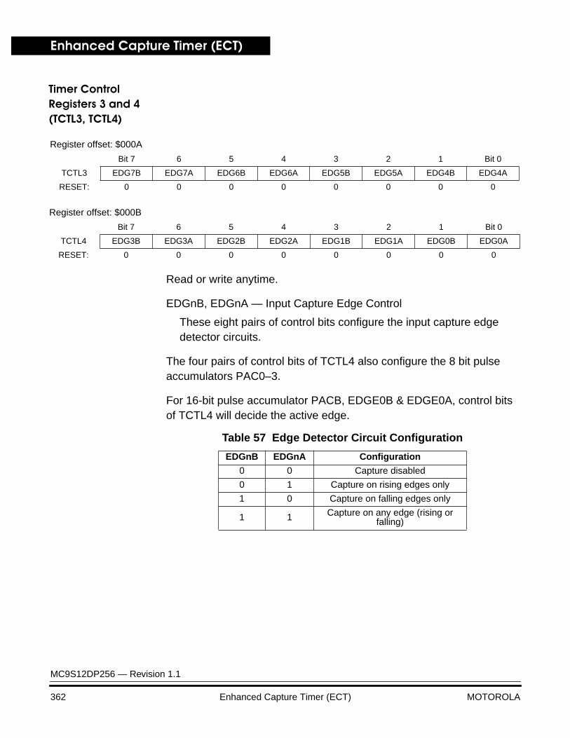
Enhanced Capture Timer (ECT)
MC9S12DP256 — Revision 1.1
362 Enhanced Capture Timer (ECT) MOTOROLA
Timer Control Registers 3 and 4 (TCTL3, TCTL4)
Read or write anytime.
EDGnB, EDGnA — Input Capture Edge Control
These eight pairs of control bits configure the input capture edge detector circuits.
The four pairs of control bits of TCTL4 also configure the 8 bit pulse accumulators PAC0–3.
For 16-bit pulse accumulator PACB, EDGE0B & EDGE0A, control bits of TCTL4 will decide the active edge.
Register offset: $000A
Bit 7 6 5 4 3 2 1 Bit 0
TCTL3 EDG7B EDG7A EDG6B EDG6A EDG5B EDG5A EDG4B EDG4A
RESET: 0 0 0 0 0 0 0 0
Register offset: $000B
Bit 7 6 5 4 3 2 1 Bit 0
TCTL4 EDG3B EDG3A EDG2B EDG2A EDG1B EDG1A EDG0B EDG0A
RESET: 0 0 0 0 0 0 0 0
Table 57 Edge Detector Circuit Configuration
EDGnB EDGnA Configuration
0 0 Capture disabled
0 1 Capture on rising edges only
1 0 Capture on falling edges only
1 1 Capture on any edge (rising or falling)
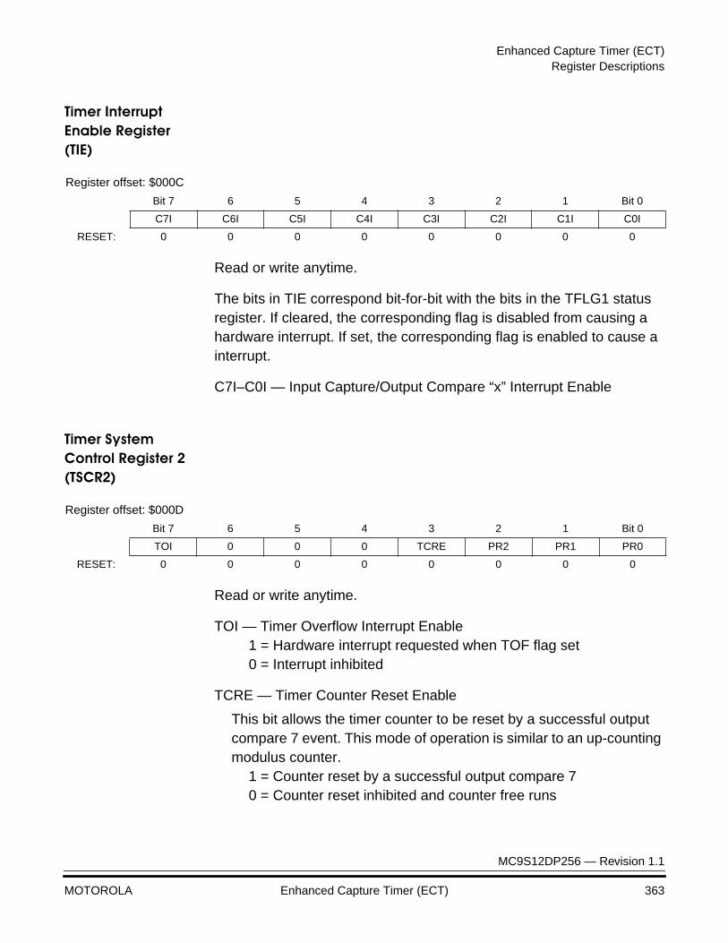
Enhanced Capture Timer (ECT)Register Descriptions
MC9S12DP256 — Revision 1.1
MOTOROLA Enhanced Capture Timer (ECT) 363
Timer Interrupt Enable Register (TIE)
Read or write anytime.
The bits in TIE correspond bit-for-bit with the bits in the TFLG1 status register. If cleared, the corresponding flag is disabled from causing a hardware interrupt. If set, the corresponding flag is enabled to cause a interrupt.
C7I–C0I — Input Capture/Output Compare “x” Interrupt Enable
Timer System Control Register 2 (TSCR2)
Read or write anytime.
TOI — Timer Overflow Interrupt Enable 1 = Hardware interrupt requested when TOF flag set0 = Interrupt inhibited
TCRE — Timer Counter Reset Enable
This bit allows the timer counter to be reset by a successful output compare 7 event. This mode of operation is similar to an up-counting modulus counter.
1 = Counter reset by a successful output compare 7 0 = Counter reset inhibited and counter free runs
Register offset: $000C
Bit 7 6 5 4 3 2 1 Bit 0
C7I C6I C5I C4I C3I C2I C1I C0I
RESET: 0 0 0 0 0 0 0 0
Register offset: $000D
Bit 7 6 5 4 3 2 1 Bit 0
TOI 0 0 0 TCRE PR2 PR1 PR0
RESET: 0 0 0 0 0 0 0 0
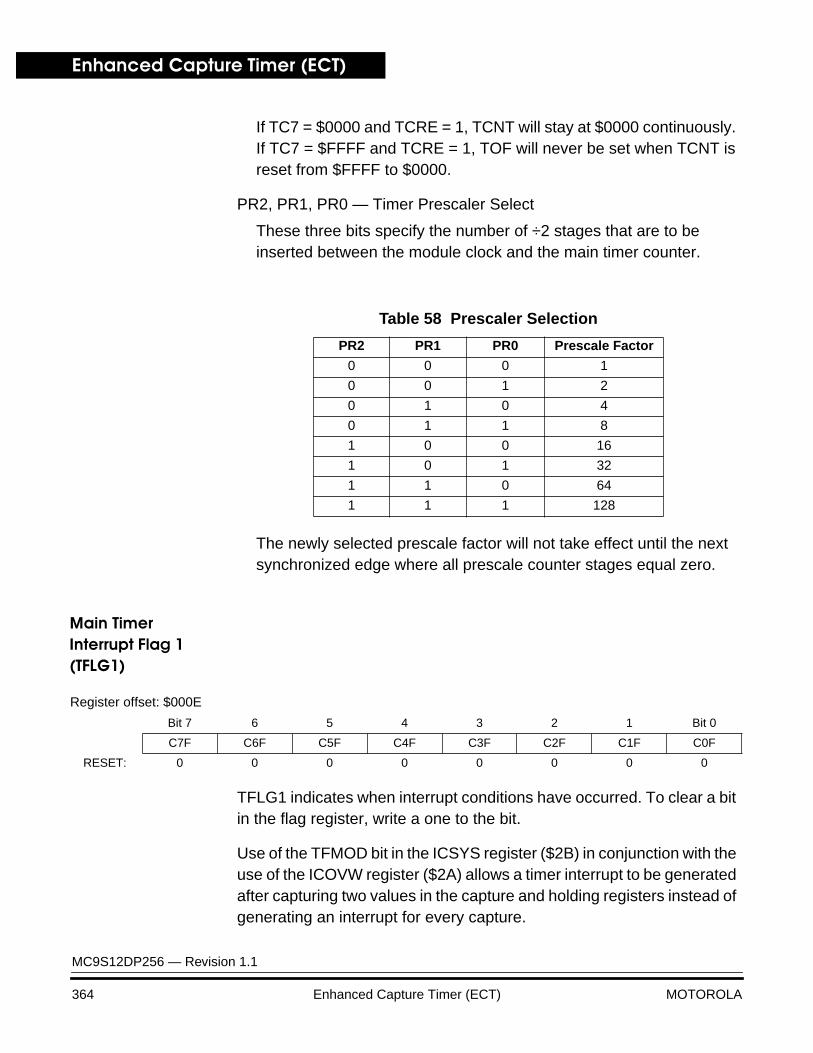
Enhanced Capture Timer (ECT)
MC9S12DP256 — Revision 1.1
364 Enhanced Capture Timer (ECT) MOTOROLA
If TC7 = $0000 and TCRE = 1, TCNT will stay at $0000 continuously. If TC7 = $FFFF and TCRE = 1, TOF will never be set when TCNT is reset from $FFFF to $0000.
PR2, PR1, PR0 — Timer Prescaler Select
These three bits specify the number of ÷2 stages that are to be inserted between the module clock and the main timer counter.
The newly selected prescale factor will not take effect until the next synchronized edge where all prescale counter stages equal zero.
Main Timer Interrupt Flag 1 (TFLG1)
TFLG1 indicates when interrupt conditions have occurred. To clear a bit in the flag register, write a one to the bit.
Use of the TFMOD bit in the ICSYS register ($2B) in conjunction with the use of the ICOVW register ($2A) allows a timer interrupt to be generated after capturing two values in the capture and holding registers instead of generating an interrupt for every capture.
Table 58 Prescaler Selection
PR2 PR1 PR0 Prescale Factor
0 0 0 1
0 0 1 2
0 1 0 4
0 1 1 8
1 0 0 16
1 0 1 32
1 1 0 64
1 1 1 128
Register offset: $000E
Bit 7 6 5 4 3 2 1 Bit 0
C7F C6F C5F C4F C3F C2F C1F C0F
RESET: 0 0 0 0 0 0 0 0
Enhanced Capture Timer (ECT)Register Descriptions
MC9S12DP256 — Revision 1.1
MOTOROLA Enhanced Capture Timer (ECT) 365
Read anytime. Write used in the clearing mechanism (set bits cause corresponding bits to be cleared). Writing a zero will not affect current status of the bit.
When TFFCA bit in TSCR register is set, a read from an input capture or a write into an output compare channel ($10–$1F) will cause the corresponding channel flag CnF to be cleared.
C7F–C0F — Input Capture/Output Compare Channel ‘n’ Flag.
C0F can also be set by 16-bit Pulse Accumulator B (PACB). C3F–C0F can also be set by 8-bit pulse accumulators PAC3–PAC0.
Main Timer Interrupt Flag 2 (TFLG2)
TFLG2 indicates when interrupt conditions have occurred. To clear a bit in the flag register, write the bit to one.
Read anytime. Write used in clearing mechanism (set bits cause corresponding bits to be cleared).
Any access to TCNT will clear TFLG2 register if the TFFCA bit in TSCR register is set.
TOF — Timer Overflow Flag
Set when 16-bit free-running timer overflows from $FFFF to $0000. This bit is cleared automatically by a write to the TFLG2 register with bit 7 set. (See also TCRE control bit explanation.)
Register offset: $000F
Bit 7 6 5 4 3 2 1 Bit 0
TOF 0 0 0 0 0 0 0
RESET: 0 0 0 0 0 0 0 0
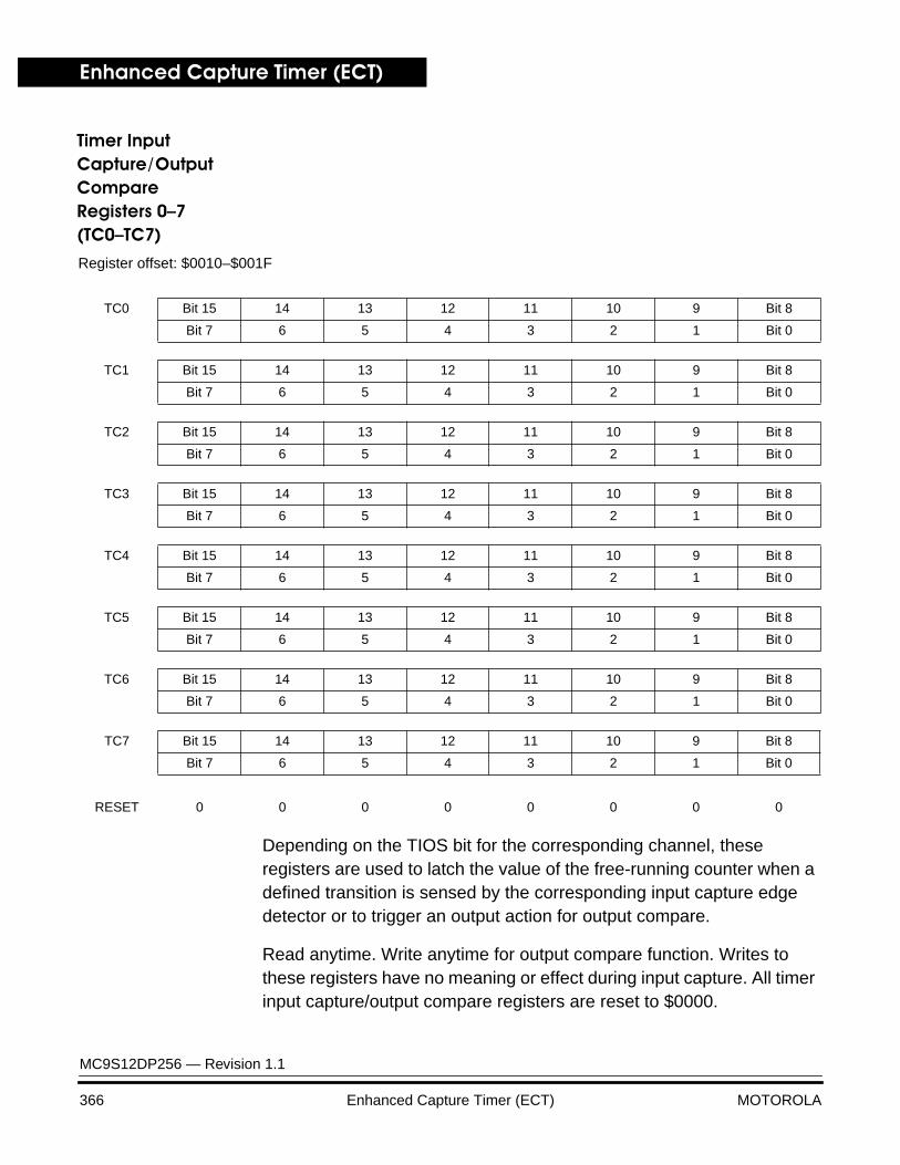
Enhanced Capture Timer (ECT)
MC9S12DP256 — Revision 1.1
366 Enhanced Capture Timer (ECT) MOTOROLA
Timer Input Capture/Output Compare Registers 0Ð7 (TC0ÐTC7)
Depending on the TIOS bit for the corresponding channel, these registers are used to latch the value of the free-running counter when a defined transition is sensed by the corresponding input capture edge detector or to trigger an output action for output compare.
Read anytime. Write anytime for output compare function. Writes to these registers have no meaning or effect during input capture. All timer input capture/output compare registers are reset to $0000.
Register offset: $0010–$001F
TC0 Bit 15 14 13 12 11 10 9 Bit 8
Bit 7 6 5 4 3 2 1 Bit 0
TC1 Bit 15 14 13 12 11 10 9 Bit 8
Bit 7 6 5 4 3 2 1 Bit 0
TC2 Bit 15 14 13 12 11 10 9 Bit 8
Bit 7 6 5 4 3 2 1 Bit 0
TC3 Bit 15 14 13 12 11 10 9 Bit 8
Bit 7 6 5 4 3 2 1 Bit 0
TC4 Bit 15 14 13 12 11 10 9 Bit 8
Bit 7 6 5 4 3 2 1 Bit 0
TC5 Bit 15 14 13 12 11 10 9 Bit 8
Bit 7 6 5 4 3 2 1 Bit 0
TC6 Bit 15 14 13 12 11 10 9 Bit 8
Bit 7 6 5 4 3 2 1 Bit 0
TC7 Bit 15 14 13 12 11 10 9 Bit 8
Bit 7 6 5 4 3 2 1 Bit 0
RESET 0 0 0 0 0 0 0 0
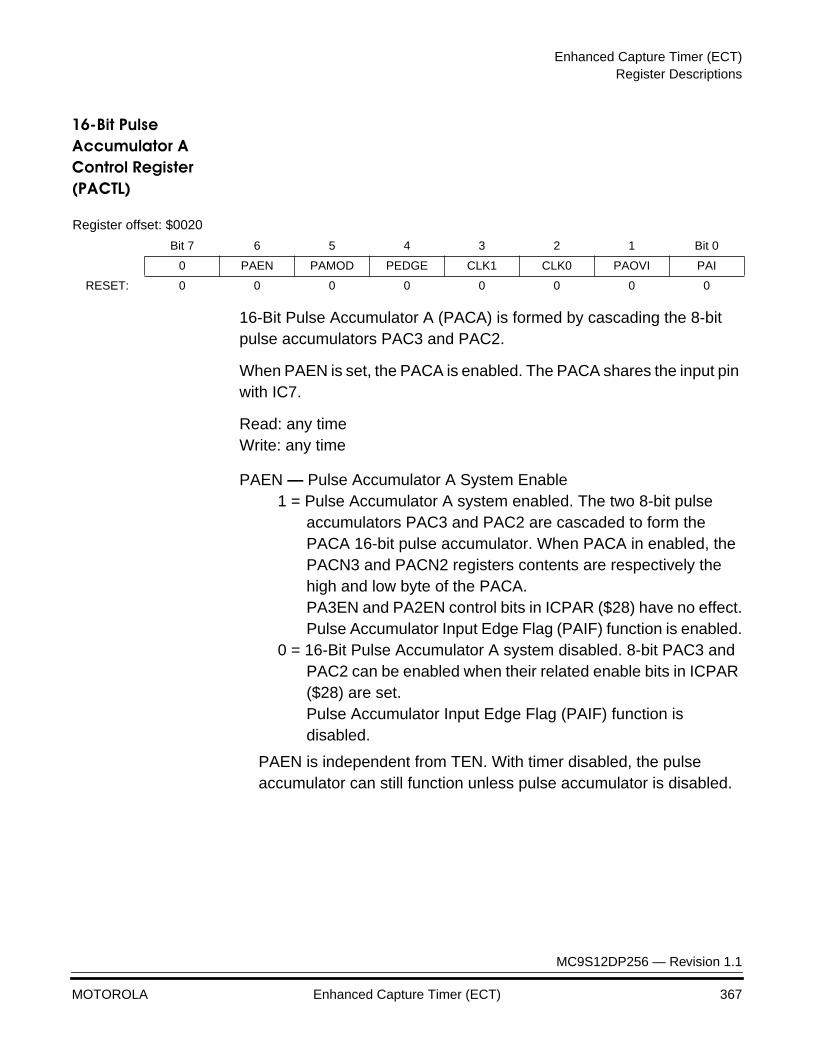
Enhanced Capture Timer (ECT)Register Descriptions
MC9S12DP256 — Revision 1.1
MOTOROLA Enhanced Capture Timer (ECT) 367
16-Bit Pulse Accumulator A Control Register (PACTL)
16-Bit Pulse Accumulator A (PACA) is formed by cascading the 8-bit pulse accumulators PAC3 and PAC2.
When PAEN is set, the PACA is enabled. The PACA shares the input pin with IC7.
Read: any timeWrite: any time
PAEN — Pulse Accumulator A System Enable 1 = Pulse Accumulator A system enabled. The two 8-bit pulse
accumulators PAC3 and PAC2 are cascaded to form the PACA 16-bit pulse accumulator. When PACA in enabled, the PACN3 and PACN2 registers contents are respectively the high and low byte of the PACA.PA3EN and PA2EN control bits in ICPAR ($28) have no effect.Pulse Accumulator Input Edge Flag (PAIF) function is enabled.
0 = 16-Bit Pulse Accumulator A system disabled. 8-bit PAC3 and PAC2 can be enabled when their related enable bits in ICPAR ($28) are set.Pulse Accumulator Input Edge Flag (PAIF) function is disabled.
PAEN is independent from TEN. With timer disabled, the pulse accumulator can still function unless pulse accumulator is disabled.
Register offset: $0020
Bit 7 6 5 4 3 2 1 Bit 0
0 PAEN PAMOD PEDGE CLK1 CLK0 PAOVI PAI
RESET: 0 0 0 0 0 0 0 0
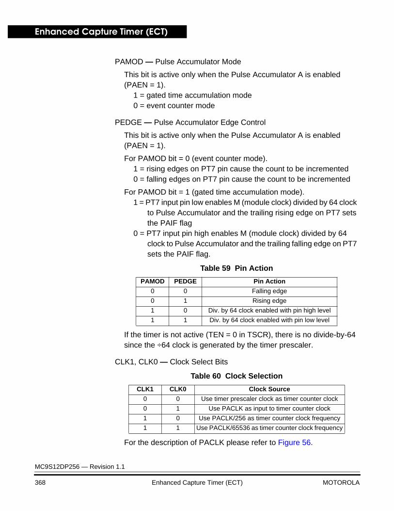
Enhanced Capture Timer (ECT)
MC9S12DP256 — Revision 1.1
368 Enhanced Capture Timer (ECT) MOTOROLA
PAMOD — Pulse Accumulator Mode
This bit is active only when the Pulse Accumulator A is enabled (PAEN = 1).
1 = gated time accumulation mode 0 = event counter mode
PEDGE — Pulse Accumulator Edge Control
This bit is active only when the Pulse Accumulator A is enabled (PAEN = 1).
For PAMOD bit = 0 (event counter mode).1 = rising edges on PT7 pin cause the count to be incremented 0 = falling edges on PT7 pin cause the count to be incremented
For PAMOD bit = 1 (gated time accumulation mode).1 = PT7 input pin low enables M (module clock) divided by 64 clock
to Pulse Accumulator and the trailing rising edge on PT7 sets the PAIF flag
0 = PT7 input pin high enables M (module clock) divided by 64 clock to Pulse Accumulator and the trailing falling edge on PT7 sets the PAIF flag.
Table 59 Pin Action
If the timer is not active (TEN = 0 in TSCR), there is no divide-by-64 since the ÷64 clock is generated by the timer prescaler.
CLK1, CLK0 — Clock Select Bits
Table 60 Clock Selection
For the description of PACLK please refer to Figure 56.
PAMOD PEDGE Pin Action
0 0 Falling edge
0 1 Rising edge
1 0 Div. by 64 clock enabled with pin high level
1 1 Div. by 64 clock enabled with pin low level
CLK1 CLK0 Clock Source
0 0 Use timer prescaler clock as timer counter clock
0 1 Use PACLK as input to timer counter clock
1 0 Use PACLK/256 as timer counter clock frequency
1 1 Use PACLK/65536 as timer counter clock frequency
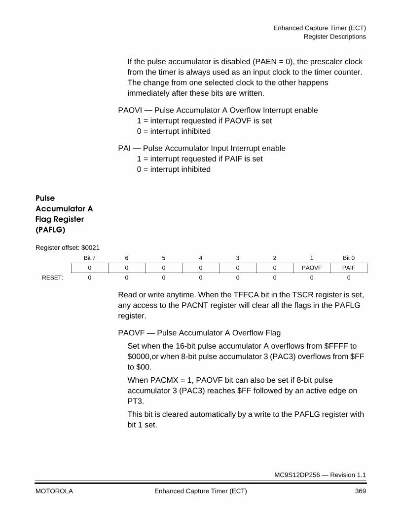
Enhanced Capture Timer (ECT)Register Descriptions
MC9S12DP256 — Revision 1.1
MOTOROLA Enhanced Capture Timer (ECT) 369
If the pulse accumulator is disabled (PAEN = 0), the prescaler clock from the timer is always used as an input clock to the timer counter. The change from one selected clock to the other happens immediately after these bits are written.
PAOVI — Pulse Accumulator A Overflow Interrupt enable1 = interrupt requested if PAOVF is set0 = interrupt inhibited
PAI — Pulse Accumulator Input Interrupt enable1 = interrupt requested if PAIF is set0 = interrupt inhibited
Pulse Accumulator A Flag Register (PAFLG)
Read or write anytime. When the TFFCA bit in the TSCR register is set, any access to the PACNT register will clear all the flags in the PAFLG register.
PAOVF — Pulse Accumulator A Overflow Flag
Set when the 16-bit pulse accumulator A overflows from $FFFF to $0000,or when 8-bit pulse accumulator 3 (PAC3) overflows from $FF to $00.
When PACMX = 1, PAOVF bit can also be set if 8-bit pulse accumulator 3 (PAC3) reaches $FF followed by an active edge on PT3.
This bit is cleared automatically by a write to the PAFLG register with bit 1 set.
Register offset: $0021
Bit 7 6 5 4 3 2 1 Bit 0
0 0 0 0 0 0 PAOVF PAIF
RESET: 0 0 0 0 0 0 0 0
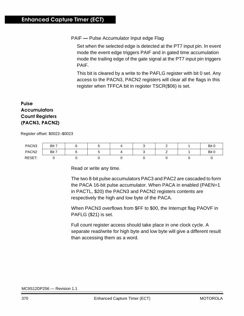
Enhanced Capture Timer (ECT)
MC9S12DP256 — Revision 1.1
370 Enhanced Capture Timer (ECT) MOTOROLA
PAIF — Pulse Accumulator Input edge Flag
Set when the selected edge is detected at the PT7 input pin. In event mode the event edge triggers PAIF and in gated time accumulation mode the trailing edge of the gate signal at the PT7 input pin triggers PAIF.
This bit is cleared by a write to the PAFLG register with bit 0 set. Any access to the PACN3, PACN2 registers will clear all the flags in this register when TFFCA bit in register TSCR($06) is set.
Pulse Accumulators Count Registers (PACN3, PACN2)
Read or write any time.
The two 8-bit pulse accumulators PAC3 and PAC2 are cascaded to form the PACA 16-bit pulse accumulator. When PACA in enabled (PAEN=1 in PACTL, $20) the PACN3 and PACN2 registers contents are respectively the high and low byte of the PACA.
When PACN3 overflows from $FF to $00, the Interrupt flag PAOVF in PAFLG ($21) is set.
Full count register access should take place in one clock cycle. A separate read/write for high byte and low byte will give a different result than accessing them as a word.
Register offset: $0022–$0023
PACN3 BIt 7 6 5 4 3 2 1 Bit 0
PACN2 Bit 7 6 5 4 3 2 1 Bit 0
RESET: 0 0 0 0 0 0 0 0
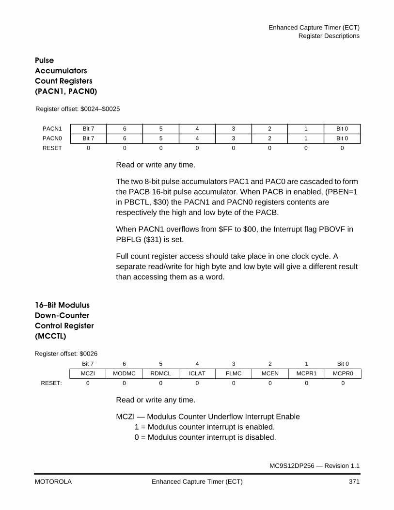
Enhanced Capture Timer (ECT)Register Descriptions
MC9S12DP256 — Revision 1.1
MOTOROLA Enhanced Capture Timer (ECT) 371
Pulse Accumulators Count Registers (PACN1, PACN0)
Read or write any time.
The two 8-bit pulse accumulators PAC1 and PAC0 are cascaded to form the PACB 16-bit pulse accumulator. When PACB in enabled, (PBEN=1 in PBCTL, $30) the PACN1 and PACN0 registers contents are respectively the high and low byte of the PACB.
When PACN1 overflows from $FF to $00, the Interrupt flag PBOVF in PBFLG ($31) is set.
Full count register access should take place in one clock cycle. A separate read/write for high byte and low byte will give a different result than accessing them as a word.
16ÐBit Modulus Down-Counter Control Register (MCCTL)
Read or write any time.
MCZI — Modulus Counter Underflow Interrupt Enable1 = Modulus counter interrupt is enabled.0 = Modulus counter interrupt is disabled.
Register offset: $0024–$0025
PACN1 Bit 7 6 5 4 3 2 1 Bit 0
PACN0 Bit 7 6 5 4 3 2 1 Bit 0
RESET 0 0 0 0 0 0 0 0
Register offset: $0026
Bit 7 6 5 4 3 2 1 Bit 0
MCZI MODMC RDMCL ICLAT FLMC MCEN MCPR1 MCPR0
RESET: 0 0 0 0 0 0 0 0

Enhanced Capture Timer (ECT)
MC9S12DP256 — Revision 1.1
372 Enhanced Capture Timer (ECT) MOTOROLA
MODMC — Modulus Mode Enable1 = Modulus mode is enabled. When the counter reaches $0000,
the counter is loaded with the latest value written to the modulus count register.
0 = The counter counts once from the value written to it and will stop at $0000.
NOTE: For proper operation, the MCEN bit should be cleared before modifying the MODMC bit in order to reset the modulus counter to $FFFF.
RDMCL — Read Modulus Down-Counter Load1 = Reads of the modulus count register will return the contents of
the load register.0 = Reads of the modulus count register will return the present
value of the count register.
ICLAT — Input Capture Force Latch Action
When input capture latch mode is enabled (LATQ and BUFEN bit in ICSYS ($2B) are set, a write one to this bit immediately forces the contents of the input capture registers TC0 to TC3 and their corresponding 8-bit pulse accumulators to be latched into the associated holding registers. The pulse accumulators will be automatically cleared when the latch action occurs.
Writing zero to this bit has no effect. Read of this bit will return always zero.
FLMC — Force Load Register into the Modulus Counter Count Register
This bit is active only when the modulus down-counter is enabled (MCEN=1).
A write one into this bit loads the load register into the modulus counter count register. This also resets the modulus counter prescaler.
Write zero to this bit has no effect.
When MODMC=0, counter starts counting and stops at $0000.
Read of this bit will return always zero.
MCEN — Modulus Down-Counter Enable1 = Modulus counter is enabled.0 = Modulus counter disabled.
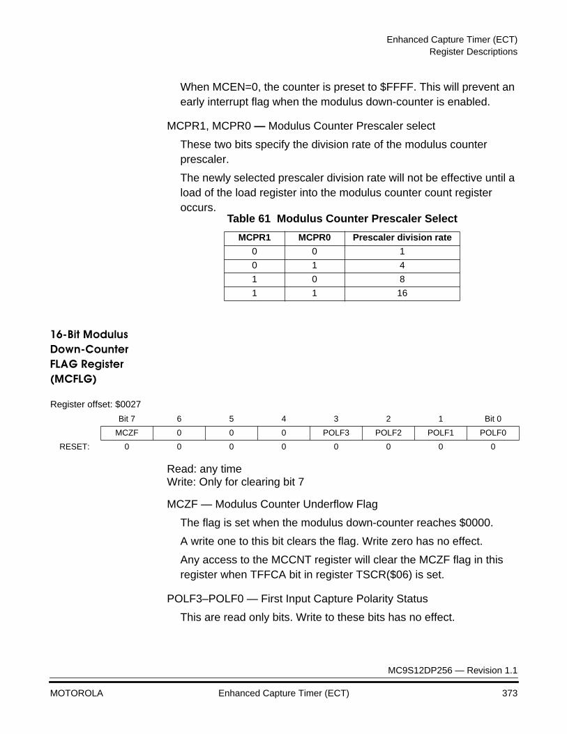
Enhanced Capture Timer (ECT)Register Descriptions
MC9S12DP256 — Revision 1.1
MOTOROLA Enhanced Capture Timer (ECT) 373
When MCEN=0, the counter is preset to $FFFF. This will prevent an early interrupt flag when the modulus down-counter is enabled.
MCPR1, MCPR0 — Modulus Counter Prescaler select
These two bits specify the division rate of the modulus counter prescaler.
The newly selected prescaler division rate will not be effective until a load of the load register into the modulus counter count register occurs.
16-Bit Modulus Down-Counter FLAG Register (MCFLG)
Read: any timeWrite: Only for clearing bit 7
MCZF — Modulus Counter Underflow Flag
The flag is set when the modulus down-counter reaches $0000.
A write one to this bit clears the flag. Write zero has no effect.
Any access to the MCCNT register will clear the MCZF flag in this register when TFFCA bit in register TSCR($06) is set.
POLF3–POLF0 — First Input Capture Polarity Status
This are read only bits. Write to these bits has no effect.
Table 61 Modulus Counter Prescaler Select
MCPR1 MCPR0 Prescaler division rate
0 0 1
0 1 4
1 0 8
1 1 16
Register offset: $0027
Bit 7 6 5 4 3 2 1 Bit 0
MCZF 0 0 0 POLF3 POLF2 POLF1 POLF0
RESET: 0 0 0 0 0 0 0 0
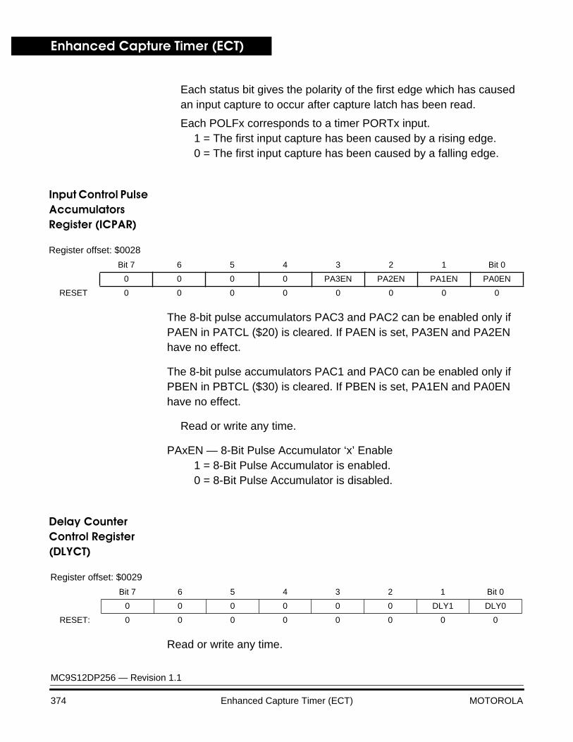
Enhanced Capture Timer (ECT)
MC9S12DP256 — Revision 1.1
374 Enhanced Capture Timer (ECT) MOTOROLA
Each status bit gives the polarity of the first edge which has caused an input capture to occur after capture latch has been read.
Each POLFx corresponds to a timer PORTx input.1 = The first input capture has been caused by a rising edge.0 = The first input capture has been caused by a falling edge.
Input Control Pulse Accumulators Register (ICPAR)
The 8-bit pulse accumulators PAC3 and PAC2 can be enabled only if PAEN in PATCL ($20) is cleared. If PAEN is set, PA3EN and PA2EN have no effect.
The 8-bit pulse accumulators PAC1 and PAC0 can be enabled only if PBEN in PBTCL ($30) is cleared. If PBEN is set, PA1EN and PA0EN have no effect.
Read or write any time.
PAxEN — 8-Bit Pulse Accumulator ‘x’ Enable1 = 8-Bit Pulse Accumulator is enabled.0 = 8-Bit Pulse Accumulator is disabled.
Delay Counter Control Register (DLYCT)
Read or write any time.
Register offset: $0028
Bit 7 6 5 4 3 2 1 Bit 0
0 0 0 0 PA3EN PA2EN PA1EN PA0EN
RESET 0 0 0 0 0 0 0 0
Register offset: $0029
Bit 7 6 5 4 3 2 1 Bit 0
0 0 0 0 0 0 DLY1 DLY0
RESET: 0 0 0 0 0 0 0 0
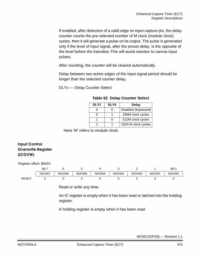
Enhanced Capture Timer (ECT)Register Descriptions
MC9S12DP256 — Revision 1.1
MOTOROLA Enhanced Capture Timer (ECT) 375
If enabled, after detection of a valid edge on input capture pin, the delay counter counts the pre-selected number of M clock (module clock) cycles, then it will generate a pulse on its output. The pulse is generated only if the level of input signal, after the preset delay, is the opposite of the level before the transition.This will avoid reaction to narrow input pulses.
After counting, the counter will be cleared automatically.
Delay between two active edges of the input signal period should be longer than the selected counter delay.
DLYx — Delay Counter Select
Here ‘M’ refers to module clock.
Input Control Overwrite Register (ICOVW)
Read or write any time.
An IC register is empty when it has been read or latched into the holding register.
A holding register is empty when it has been read.
Table 62 Delay Counter Select
DLY1 DLY0 Delay
0 0 Disabled (bypassed)
0 1 256M clock cycles
1 0 512M clock cycles
1 1 1024 M clock cycles
Register offset: $002A
Bit 7 6 5 4 3 2 1 Bit 0
NOVW7 NOVW6 NOVW5 NOVW4 NOVW3 NOVW2 NOVW1 NOVW0
RESET: 0 0 0 0 0 0 0 0
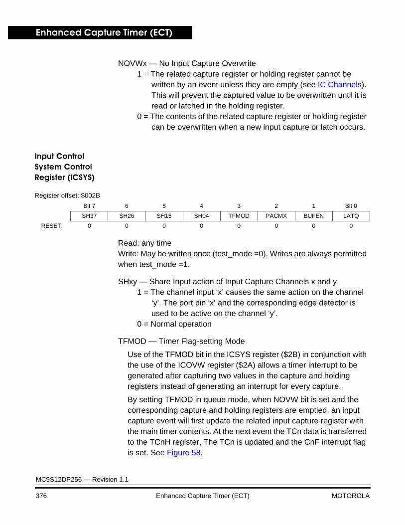
Enhanced Capture Timer (ECT)
MC9S12DP256 — Revision 1.1
376 Enhanced Capture Timer (ECT) MOTOROLA
NOVWx — No Input Capture Overwrite 1 = The related capture register or holding register cannot be
written by an event unless they are empty (see IC Channels). This will prevent the captured value to be overwritten until it is read or latched in the holding register.
0 = The contents of the related capture register or holding register can be overwritten when a new input capture or latch occurs.
Input Control System Control Register (ICSYS)
Read: any timeWrite: May be written once (test_mode =0). Writes are always permitted when test_mode =1.
SHxy — Share Input action of Input Capture Channels x and y1 = The channel input ‘x’ causes the same action on the channel
‘y’. The port pin ‘x’ and the corresponding edge detector is used to be active on the channel ‘y’.
0 = Normal operation
TFMOD — Timer Flag-setting Mode
Use of the TFMOD bit in the ICSYS register ($2B) in conjunction with the use of the ICOVW register ($2A) allows a timer interrupt to be generated after capturing two values in the capture and holding registers instead of generating an interrupt for every capture.
By setting TFMOD in queue mode, when NOVW bit is set and the corresponding capture and holding registers are emptied, an input capture event will first update the related input capture register with the main timer contents. At the next event the TCn data is transferred to the TCnH register, The TCn is updated and the CnF interrupt flag is set. See Figure 58.
Register offset: $002B
Bit 7 6 5 4 3 2 1 Bit 0
SH37 SH26 SH15 SH04 TFMOD PACMX BUFEN LATQ
RESET: 0 0 0 0 0 0 0 0
Enhanced Capture Timer (ECT)Register Descriptions
MC9S12DP256 — Revision 1.1
MOTOROLA Enhanced Capture Timer (ECT) 377
In all other input capture cases the interrupt flag is set by a valid external event on PTn.
1 = If in queue mode (BUFEN=1 and LATQ=0), the timer flags C3F–C0F in TFLG1 ($0E) are set only when a latch on the corresponding holding register occurs.If the queue mode is not engaged, the timer flags C3F–C0F are set the same way as for TFMOD=0.
0 = The timer flags C3F–C0F in TFLG1 ($0E) are set when a valid input capture transition on the corresponding port pin occurs.
PACMX — 8-Bit Pulse Accumulators Maximum Count1 = When the 8-bit pulse accumulator has reached the value $FF,
it will not be incremented further. The value $FF indicates a count of 255 or more.
0 = Normal operation. When the 8-bit pulse accumulator has reached the value $FF, with the next active edge, it will be incremented to $00.
BUFEN — IC Buffer Enable1 = Input Capture and pulse accumulator holding registers are
enabled. The latching mode is defined by LATQ control bit.Write one into ICLAT bit in MCCTL ($26), when LATQ is set will produce latching of input capture and pulse accumulators registers into their holding registers.
0 = Input Capture and pulse accumulator holding registers are disabled.
LATQ — Input Control Latch or Queue Mode Enable
The BUFEN control bit should be set in order to enable the IC and pulse accumulators holding registers. Otherwise LATQ latching modes are disabled.
Write one into ICLAT bit in MCCTL ($26), when LATQ and BUFEN are set will produce latching of input capture and pulse accumulators registers into their holding registers.
1 = Latch Mode is enabled. Latching function occurs when modulus down-counter reaches zero or a zero is written into the count register MCCNT (see Buffered IC Channels).
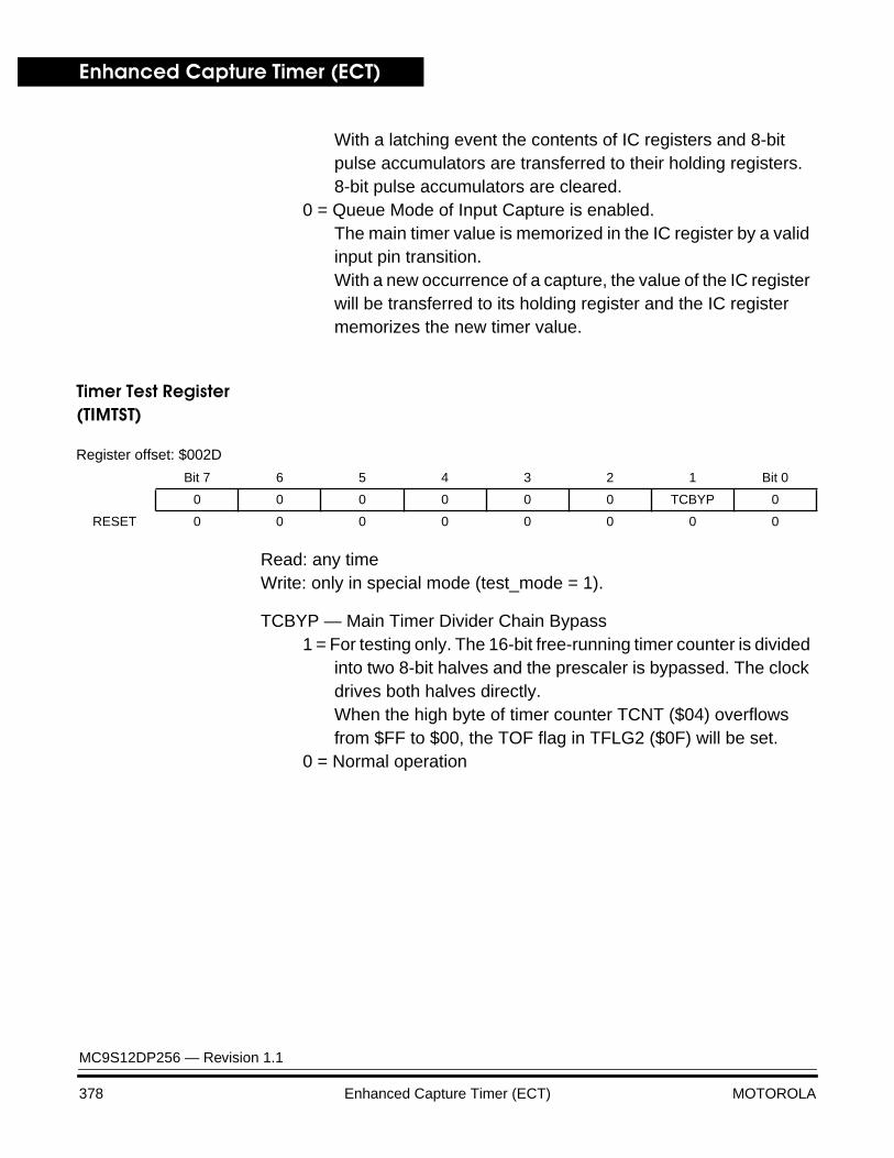
Enhanced Capture Timer (ECT)
MC9S12DP256 — Revision 1.1
378 Enhanced Capture Timer (ECT) MOTOROLA
With a latching event the contents of IC registers and 8-bit pulse accumulators are transferred to their holding registers.8-bit pulse accumulators are cleared.
0 = Queue Mode of Input Capture is enabled.The main timer value is memorized in the IC register by a valid input pin transition.With a new occurrence of a capture, the value of the IC register will be transferred to its holding register and the IC register memorizes the new timer value.
Timer Test Register (TIMTST)
Read: any timeWrite: only in special mode (test_mode = 1).
TCBYP — Main Timer Divider Chain Bypass 1 = For testing only. The 16-bit free-running timer counter is divided
into two 8-bit halves and the prescaler is bypassed. The clock drives both halves directly.When the high byte of timer counter TCNT ($04) overflows from $FF to $00, the TOF flag in TFLG2 ($0F) will be set.
0 = Normal operation
Register offset: $002D
Bit 7 6 5 4 3 2 1 Bit 0
0 0 0 0 0 0 TCBYP 0
RESET 0 0 0 0 0 0 0 0
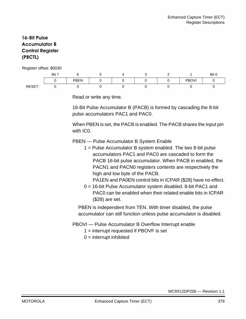
Enhanced Capture Timer (ECT)Register Descriptions
MC9S12DP256 — Revision 1.1
MOTOROLA Enhanced Capture Timer (ECT) 379
16-Bit Pulse Accumulator B Control Register (PBCTL)
Read or write any time.
16-Bit Pulse Accumulator B (PACB) is formed by cascading the 8-bit pulse accumulators PAC1 and PAC0.
When PBEN is set, the PACB is enabled. The PACB shares the input pin with IC0.
PBEN — Pulse Accumulator B System Enable 1 = Pulse Accumulator B system enabled. The two 8-bit pulse
accumulators PAC1 and PAC0 are cascaded to form the PACB 16-bit pulse accumulator. When PACB in enabled, the PACN1 and PACN0 registers contents are respectively the high and low byte of the PACB.PA1EN and PA0EN control bits in ICPAR ($28) have no effect.
0 = 16-bit Pulse Accumulator system disabled. 8-bit PAC1 and PAC0 can be enabled when their related enable bits in ICPAR ($28) are set.
PBEN is independent from TEN. With timer disabled, the pulse accumulator can still function unless pulse accumulator is disabled.
PBOVI — Pulse Accumulator B Overflow Interrupt enable1 = interrupt requested if PBOVF is set0 = interrupt inhibited
Register offset: $0030
Bit 7 6 5 4 3 2 1 Bit 0
0 PBEN 0 0 0 0 PBOVI 0
RESET: 0 0 0 0 0 0 0 0
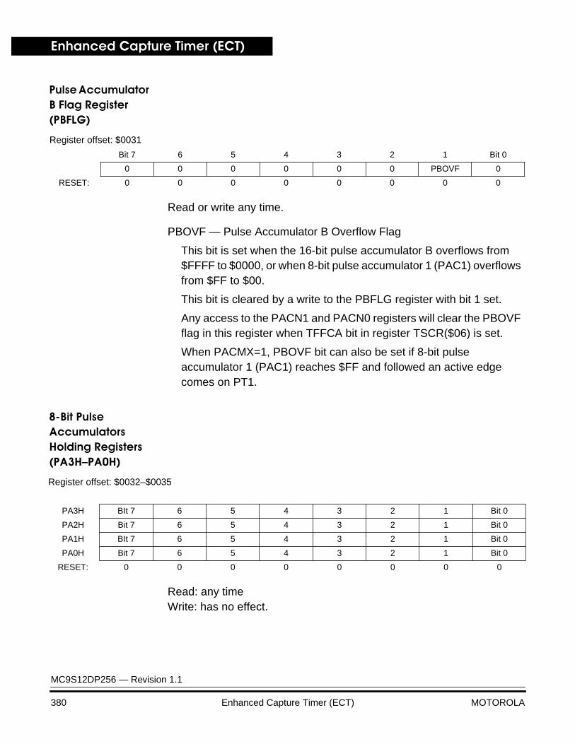
Enhanced Capture Timer (ECT)
MC9S12DP256 — Revision 1.1
380 Enhanced Capture Timer (ECT) MOTOROLA
Pulse Accumulator B Flag Register (PBFLG)
Read or write any time.
PBOVF — Pulse Accumulator B Overflow Flag
This bit is set when the 16-bit pulse accumulator B overflows from $FFFF to $0000, or when 8-bit pulse accumulator 1 (PAC1) overflows from $FF to $00.
This bit is cleared by a write to the PBFLG register with bit 1 set.
Any access to the PACN1 and PACN0 registers will clear the PBOVF flag in this register when TFFCA bit in register TSCR($06) is set.
When PACMX=1, PBOVF bit can also be set if 8-bit pulse accumulator 1 (PAC1) reaches $FF and followed an active edge comes on PT1.
8-Bit Pulse Accumulators Holding Registers (PA3HÐPA0H)
Read: any timeWrite: has no effect.
Register offset: $0031
Bit 7 6 5 4 3 2 1 Bit 0
0 0 0 0 0 0 PBOVF 0
RESET: 0 0 0 0 0 0 0 0
Register offset: $0032–$0035
PA3H BIt 7 6 5 4 3 2 1 Bit 0
PA2H Bit 7 6 5 4 3 2 1 Bit 0
PA1H BIt 7 6 5 4 3 2 1 Bit 0
PA0H Bit 7 6 5 4 3 2 1 Bit 0
RESET: 0 0 0 0 0 0 0 0

Enhanced Capture Timer (ECT)Register Descriptions
MC9S12DP256 — Revision 1.1
MOTOROLA Enhanced Capture Timer (ECT) 381
These registers are used to latch the value of the corresponding pulse accumulator when the related bits in register ICPAR ($28) are enabled (see Pulse Accumulators).
Modulus Down-Counter Count Register (MCCNT)
Read or write any time.
A full access for the counter register should take place in one clock cycle. A separate read/write for high byte and low byte will give different result than accessing them as a word.
If the RDMCL bit in MCCTL register is cleared, reads of the MCCNT register will return the present value of the count register. If the RDMCL bit is set, reads of the MCCNT will return the contents of the load register.
If a $0000 is written into MCCNT and modulus counter while LATQ and BUFEN in ICSYS ($2B) register are set, the input capture and pulse accumulator registers will be latched.
With a $0000 write to the MCCNT, the modulus counter will stay at zero and does not set the MCZF flag in MCFLG register.
If modulus mode is enabled (MODMC=1), a write to this address will update the load register with the value written to it. The count register will not be updated with the new value until the next counter underflow.
The FLMC bit in MCCTL ($26) can be used to immediately update the count register with the new value if an immediate load is desired.
Register offset: $0036–$0037
BIt 15 14 13 12 11 10 9 Bit 8
Bit 7 6 5 4 3 2 1 Bit 0
RESET: 1 1 1 1 1 1 1 1

Enhanced Capture Timer (ECT)
MC9S12DP256 — Revision 1.1
382 Enhanced Capture Timer (ECT) MOTOROLA
If modulus mode is not enabled (MODMC=0), a write to this address will clear the prescaler and will immediately update the counter register with the value written to it and down-counts once to $0000
Timer Input Capture Holding Registers 0Ð3 (TC0HÐTC3H)
Read: any timeWrite: has no effect.
These registers are used to latch the value of the input capture registers TC0–TC3. The corresponding IOSx bits in TIOS ($00) should be cleared (see IC Channels).
Register offset: $0038–$003F
TC0H Bit 15 14 13 12 11 10 9 Bit 8
Bit 7 6 5 4 3 2 1 Bit 0
TC1H Bit 15 14 13 12 11 10 9 Bit 8
Bit 7 6 5 4 3 2 1 Bit 0
TC2H Bit 15 14 13 12 11 10 9 Bit 8
Bit 7 6 5 4 3 2 1 Bit 0
TC3H Bit 15 14 13 12 11 10 9 Bit 8
Bit 7 6 5 4 3 2 1 Bit 0
RESET 0 0 0 0 0 0 0 0
Enhanced Capture Timer (ECT)Modes of Operation
MC9S12DP256 — Revision 1.1
MOTOROLA Enhanced Capture Timer (ECT) 383
Modes of Operation
The Enhanced Capture Timer has 8 Input Capture, Output Compare (IC/OC) channels same as on the HC12 standard timer (timer channels TC0 to TC7). When channels are selected as input capture by selecting the IOSx bit in TIOS register, they are called Input Capture (IC) channels.
Four IC channels are the same as on the standard timer with one capture register each which memorizes the timer value captured by an action on the associated input pin.
Four other IC channels, in addition to the capture register, have also one buffer each called holding register. This permits to memorize two different timer values without generation of any interrupt.
Four 8-bit pulse accumulators are associated with the four buffered IC channels. Each pulse accumulator has a holding register to memorize their value by an action on its external input. Each pair of pulse accumulators can be used as a 16-bit pulse accumulator.
The 16-bit modulus down-counter can control the transfer of the IC registers contents and the pulse accumulators to the respective holding registers for a given period, every time the count reaches zero.
The modulus down-counter can also be used as a stand-alone time base with periodic interrupt capability.
IC Channels The IC channels are composed of four standard IC registers and four buffered IC channels.
An IC register is empty when it has been read or latched into the holding register.
A holding register is empty when it has been read.
Non-Buffered IC Channels
The main timer value is memorized in the IC register by a valid input pin transition. If the corresponding NOVWx bit of the ICOVW register is
Enhanced Capture Timer (ECT)
MC9S12DP256 — Revision 1.1
384 Enhanced Capture Timer (ECT) MOTOROLA
cleared, with a new occurrence of a capture, the contents of IC register are overwritten by the new value.
If the corresponding NOVWx bit of the ICOVW register is set, the capture register cannot be written unless it is empty.
This will prevent the captured value to be overwritten until it is read.
Buffered IC Channels
There are two modes of operations for the buffered IC channels.
• IC Latch Mode:
When enabled (LATQ=1), the main timer value is memorized in the IC register by a valid input pin transition.
The value of the buffered IC register is latched to its holding register by the Modulus counter for a given period when the count reaches zero, by a write $0000 to the modulus counter or by a write to ICLAT in the MCCTL register.
If the corresponding NOVWx bit of the ICOVW register is cleared, with a new occurrence of a capture, the contents of IC register are overwritten by the new value. In case of latching, the contents of its holding register are overwritten.
If the corresponding NOVWx bit of the ICOVW register is set, the capture register or its holding register cannot be written by an event unless they are empty (see IC Channels). This will prevent the captured value to be overwritten until it is read or latched in the holding register.
• IC queue mode:
When enabled (LATQ=0), the main timer value is memorized in the IC register by a valid input pin transition.
If the corresponding NOVWx bit of the ICOVW register is cleared, with a new occurrence of a capture, the value of the IC register will be transferred to its holding register and the IC register memorizes the new timer value.
If the corresponding NOVWx bit of the ICOVW register is set, the capture register or its holding register cannot be written by an event unless they are empty (see IC Channels).
Enhanced Capture Timer (ECT)Modes of Operation
MC9S12DP256 — Revision 1.1
MOTOROLA Enhanced Capture Timer (ECT) 385
In queue mode, reads of holding register will latch the corresponding pulse accumulator value to its holding register.
Pulse Accumulators
There are four 8-bit pulse accumulators with four 8-bit holding registers associated with the four IC buffered channels. A pulse accumulator counts the number of active edges at the input of its channel.
The user can prevent 8-bit pulse accumulators counting further than $FF by PACMX control bit in ICSYS ($2B). In this case a value of $FF means that 255 counts or more have occurred.
Each pair of pulse accumulators can be used as a 16-bit pulse accumulator.
There are two modes of operation for the pulse accumulators.
Pulse Accumulator latch mode
The value of the pulse accumulator is transferred to its holding register when the modulus down-counter reaches zero, a write $0000 to the modulus counter or when the force latch control bit ICLAT is written.
At the same time the pulse accumulator is cleared.
Pulse Accumulator queue mode
When queue mode is enabled, reads of an input capture holding register will transfer the contents of the associated pulse accumulator to its holding register.
At the same time the pulse accumulator is cleared.
Modulus Down-Counter
The modulus down-counter can be used as a time base to generate a periodic interrupt. It can also be used to latch the values of the IC registers and the pulse accumulators to their holding registers.
The action of latching can be programmed to be periodic or only once.
Enhanced Capture Timer (ECT)
MC9S12DP256 — Revision 1.1
386 Enhanced Capture Timer (ECT) MOTOROLA
Interrupts
This section describes interrupts originated by the ECT block.The MCU must service the interrupt requests. Table 63 lists the interrupts generated by the ECT to communicate with the MCU.
Table 63 ECT Interrupts
InterruptOffset
(1) Vector1 Priority1 Source Description
ectch_int[7:0] – – – Timer Channel 7–0 Active high timer channel interrupts 7–0
ectmcufi_int – – –Modulus counter
underflowActive high modulus counter interrupt
ectpabo_int – – –Pulse Accumulator B
OverflowActive high pulse accumulator B interrupt
ectpaai_int – – –Pulse Accumulator A
Input Active high pulse accumulator A input interrupt
ectpaao_int – – –Pulse Accumulator A
OverflowPulse accumulator overflow interrupt
ectovi_int – – – Timer Overflow Timer Overflow interrupt
1. Chip Dependent

Enhanced Capture Timer (ECT)Description of Interrupt Operation
MC9S12DP256 — Revision 1.1
MOTOROLA Enhanced Capture Timer (ECT) 387
Description of Interrupt Operation
The ECT only originates interrupt requests. The following is a description of how the ECT makes a request and how the MCU should acknowledge that request. The interrupt vector offset and interrupt number are chip dependent.
Channel [7:0] Interrupt (ectch_int[7:0])
This active high output will be asserted by the module to request a timer channel 7–0 interrupt to be serviced by the system controller.
Modulus Counter Interrupt (ectmcufi_int)
This active high output will be asserted by the module to request a modulus counter underflow interrupt to be serviced by the system controller.
Pulse Accumulator B Overflow Interrupt (ectpabo_int)
This active high output will be asserted by the module to request a timer pulse accumulator B overflow interrupt to be serviced by the system controller.
Pulse Accumulator A Input Interrupt (ectpaai_int)
This active high output will be asserted by the module to request a timer pulse accumulator A input interrupt to be serviced by the system controller.
Pulse Accumulator A Overflow Interrupt (ectpaao_int)
This active high output will be asserted by the module to request a timer pulse accumulator A overflow interrupt to be serviced by the system controller.
Timer Overflow Interrupt (ectovi_int)
This active high output will be asserted by the module to request a timer overflow interrupt to be serviced by the system controller.

Enhanced Capture Timer (ECT)
MC9S12DP256 — Revision 1.1
388 Enhanced Capture Timer (ECT) MOTOROLA
MC9S12DP256 — Revision 1.1
MOTOROLA Serial Communications Interface (SCI) 389
Serial Communications Interface (SCI)Serial Communications Interface (SCI)
Contents
Overview . . . . . . . . . . . . . . . . . . . . . . . . . . . . . . . . . . . . . . . . . . . . . . 389Features . . . . . . . . . . . . . . . . . . . . . . . . . . . . . . . . . . . . . . . . . . . . . . 389Modes of Operation. . . . . . . . . . . . . . . . . . . . . . . . . . . . . . . . . . . . . . 390SCI Interface Diagram. . . . . . . . . . . . . . . . . . . . . . . . . . . . . . . . . . . . 392Block Diagram. . . . . . . . . . . . . . . . . . . . . . . . . . . . . . . . . . . . . . . . . . 392Signal Descriptions . . . . . . . . . . . . . . . . . . . . . . . . . . . . . . . . . . . . . . 393Module Memory Map . . . . . . . . . . . . . . . . . . . . . . . . . . . . . . . . . . . . 394Register Quick Reference . . . . . . . . . . . . . . . . . . . . . . . . . . . . . . . . . 395Register Descriptions . . . . . . . . . . . . . . . . . . . . . . . . . . . . . . . . . . . . 396Functional Description. . . . . . . . . . . . . . . . . . . . . . . . . . . . . . . . . . . . 406Modes of Operation. . . . . . . . . . . . . . . . . . . . . . . . . . . . . . . . . . . . . . 424Interrupt Operation . . . . . . . . . . . . . . . . . . . . . . . . . . . . . . . . . . . . . . 425
Overview
The SCI allows asynchronous serial communications with peripheral devices and other CPUs.
Features
The SCI includes these distinctive features:
• Full-duplex operation
• Standard mark/space non-return-to-zero (NRZ) format
• 13-bit baud rate selection
• Programmable 8-bit or 9-bit data format
Serial Communications Interface (SCI)
MC9S12DP256 — Revision 1.1
390 Serial Communications Interface (SCI) MOTOROLA
• Separately enabled transmitter and receiver
• Programmable transmitter output parity
• Two receiver wakeup methods:
– Idle line wakeup
– Address mark wakeup
• Interrupt-driven operation with eight flags:
– Transmitter empty
– Transmission complete
– Receiver full
– Idle receiver input
– Receiver overrun
– Noise error
– Framing error
– Parity error
• Receiver framing error detection
• Hardware parity checking
• 10/13 bit software selectable break character length1
• 1/16 bit-time noise detection
• Fully scan testable design
Modes of Operation
The SCI functions the same in normal, special, and emulation modes. It has two low power modes, wait and stop modes.
• Run Mode
This is the basic mode of operation.
1. Th8is feature is not available on the first mask set (0K36N)
Serial Communications Interface (SCI)Modes of Operation
MC9S12DP256 — Revision 1.1
MOTOROLA Serial Communications Interface (SCI) 391
• Wait Mode
SCI operation in wait mode is a configurable low power mode. Depending on the state of internal bits, the SCI can operate normally when the CPU is in wait mode or the SCI clock generation can be turned off and the SCI module enters a power conservation state during wait mode. In the later case, any transmission or reception in progress stops at wait mode entry.
• Stop Mode
The SCI is inactive in stop mode for reduced power consumption. The STOP instruction does not affect SCI register states.

Serial Communications Interface (SCI)
MC9S12DP256 — Revision 1.1
392 Serial Communications Interface (SCI) MOTOROLA
SCI Interface Diagram
Block Diagram
Figure 63 is a block diagram of the SCI.
Figure 63 SCI Block Diagram
SCI DATA
RECEIVESHIFT REGISTER
SCI DATA REGISTER
TRANSMITSHIFT REGISTER
REGISTER
BAUD RATEGENERATOR
SBR12–SBR0
sci_rx_ind
sci_tx_do
MODULE
TRANSMITCONTROL÷16
RECEIVEAND WAKEUP
DATA FORMATCONTROL
CONTROL
T8
PF
FE
NF
RDRF
IDLE
TIE
OR
TCIE
TDRE
TC
R8
RAFLOOPS
RWU
RE
PE
ILT
PT
WAKE
M
CLOCK
IDLEILIE
RIE
RDRF/OR
TDRE
TC
INTERRUPT
INTERRUPT
INTERRUPT
INTERRUPT
RSRC
SBK
LOOPS
TE
RSRC
REQUEST
REQUEST
REQUEST
REQUEST
BRK13
TXDIR
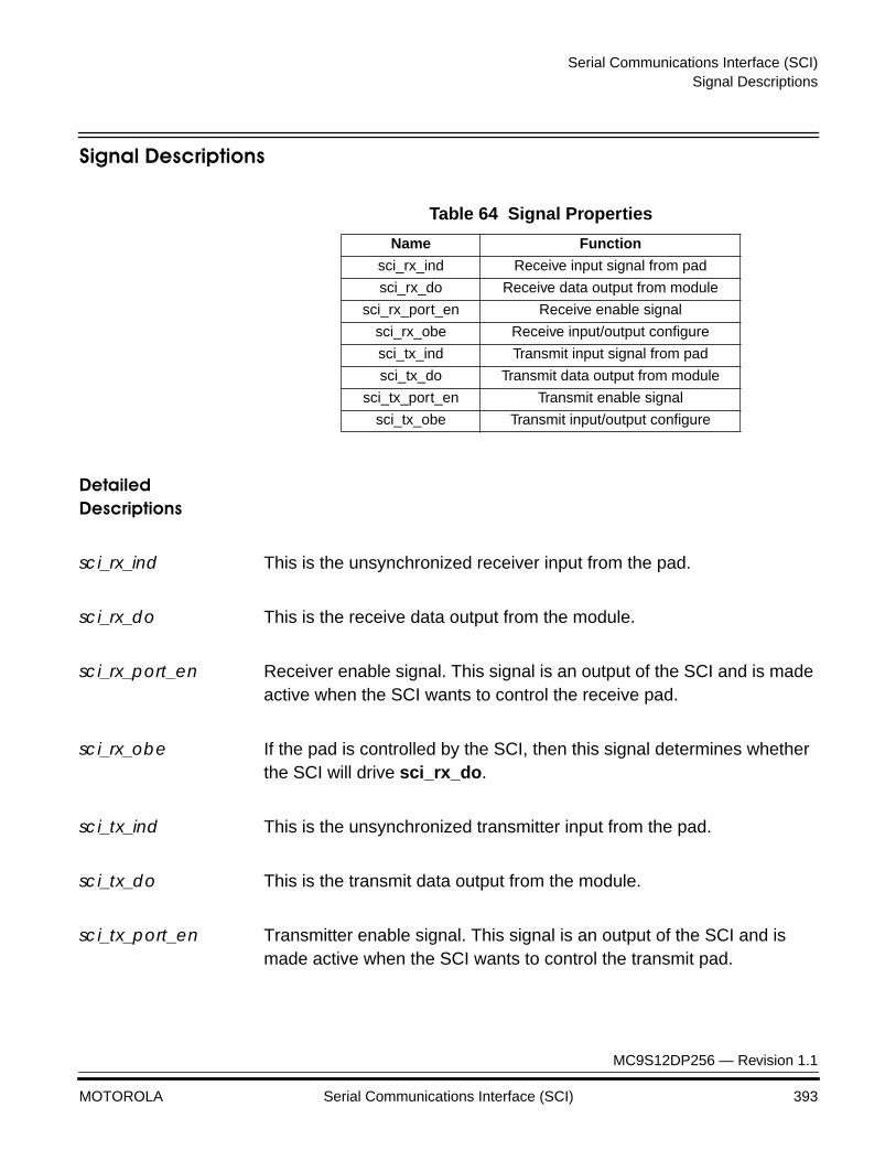
Serial Communications Interface (SCI)Signal Descriptions
MC9S12DP256 — Revision 1.1
MOTOROLA Serial Communications Interface (SCI) 393
Signal Descriptions
Detailed Descriptions
sci_rx_ind This is the unsynchronized receiver input from the pad.
sci_rx_do This is the receive data output from the module.
sci_rx_port_en Receiver enable signal. This signal is an output of the SCI and is made active when the SCI wants to control the receive pad.
sci_rx_obe If the pad is controlled by the SCI, then this signal determines whether the SCI will drive sci_rx_do.
sci_tx_ind This is the unsynchronized transmitter input from the pad.
sci_tx_do This is the transmit data output from the module.
sci_tx_port_en Transmitter enable signal. This signal is an output of the SCI and is made active when the SCI wants to control the transmit pad.
Table 64 Signal Properties
Name Function
sci_rx_ind Receive input signal from pad
sci_rx_do Receive data output from module
sci_rx_port_en Receive enable signal
sci_rx_obe Receive input/output configure
sci_tx_ind Transmit input signal from pad
sci_tx_do Transmit data output from module
sci_tx_port_en Transmit enable signal
sci_tx_obe Transmit input/output configure

Serial Communications Interface (SCI)
MC9S12DP256 — Revision 1.1
394 Serial Communications Interface (SCI) MOTOROLA
sci_tx_obe If the pad is controlled by the SCI, then this signal determines whether the SCI will drive sci_tx_do.
Interrupt Signal The SCI has one interrupt signal. Refer to the Interrupt Operation subsection for more details.
Module Memory Map
The memory map for the SCI module is given below in Table 65. The Address listed for each register is the address offset. The total address for each register is the sum of the base address for the SCI module and the address offset for each register.
Table 65 Module Memory Map
Offset Use Access
$000 SCI Baud Rate Register High (SCIBDH) Read/Write
$001 SCI Baud Rate Register Low (SCIBDL) Read/Write
$002 SCI Control Register1 (SCICR1) Read/Write
$003 SCI Control Register 2 (SCICR2) Read/Write
$004 SCI Status Register 1 (SCISR1) Read
$005 SCI Status Register 2(SCISR2) Read/Write
$006 SCI Data Register High (SCIDRH) Read/Write
$007 SCI Data Register Low (SCIDRL) Read/Write

Serial Communications Interface (SCI)Register Quick Reference
MC9S12DP256 — Revision 1.1
MOTOROLA Serial Communications Interface (SCI) 395
Register Quick Reference
Figure 64 SCI Register Quick Reference
Register name Bit 7 6 5 4 3 2 1 Bit 0 Addr. offset
SCIBDHRead: 0 0 0
SBR12 SBR11 SBR10 SBR9 SBR8 $000Write:
SCIBDLRead:
SBR7 SBR6 SBR5 SBR4 SBR3 SBR2 SBR1 SBR0 $001Write:
SCICR1Read:
LOOPS SCISWAI RSRC M WAKE ILT PE PT $002Write:
SCICR2Read:
TIE TCIE RIE ILIE TE RE RWU SBK $003Write:
SCISR1Read: TDRE TC RDRF IDLE OR NF FE PF
$004Write:
SCISR2Read: 0 0 0 0 0
BRK13 TXDIRRAF
$005Write:
SCIDRHRead: R8
T80 0 0 0 0 0
$006Write:
SCIDRLRead: R7 R6 R5 R4 R3 R2 R1 R0
$007Write: T7 T6 T5 T4 T3 T2 T1 T0
= Reserved or unimplemented
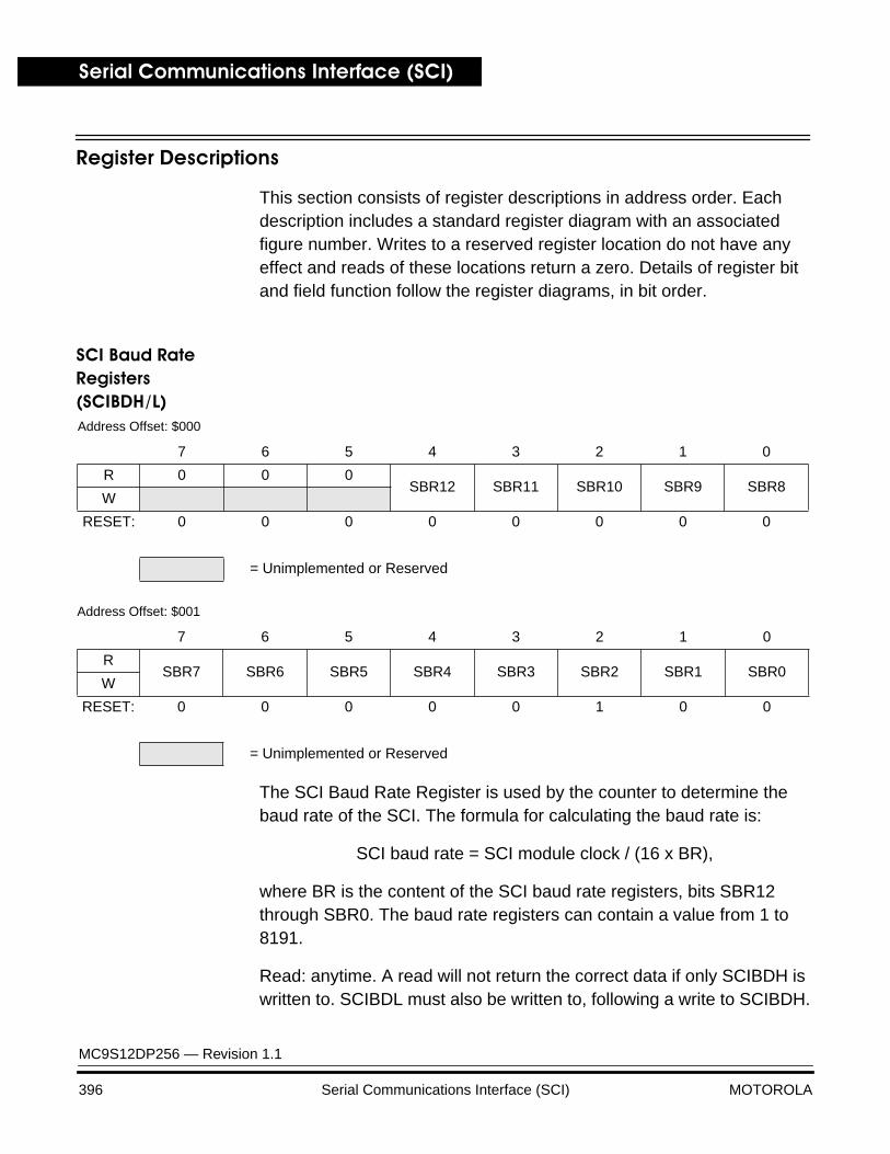
Serial Communications Interface (SCI)
MC9S12DP256 — Revision 1.1
396 Serial Communications Interface (SCI) MOTOROLA
Register Descriptions
This section consists of register descriptions in address order. Each description includes a standard register diagram with an associated figure number. Writes to a reserved register location do not have any effect and reads of these locations return a zero. Details of register bit and field function follow the register diagrams, in bit order.
SCI Baud Rate Registers (SCIBDH/L)
The SCI Baud Rate Register is used by the counter to determine the baud rate of the SCI. The formula for calculating the baud rate is:
SCI baud rate = SCI module clock / (16 x BR),
where BR is the content of the SCI baud rate registers, bits SBR12 through SBR0. The baud rate registers can contain a value from 1 to 8191.
Read: anytime. A read will not return the correct data if only SCIBDH is written to. SCIBDL must also be written to, following a write to SCIBDH.
Address Offset: $000
7 6 5 4 3 2 1 0
R 0 0 0SBR12 SBR11 SBR10 SBR9 SBR8
W
RESET: 0 0 0 0 0 0 0 0
= Unimplemented or Reserved
Address Offset: $001
7 6 5 4 3 2 1 0
RSBR7 SBR6 SBR5 SBR4 SBR3 SBR2 SBR1 SBR0
W
RESET: 0 0 0 0 0 1 0 0
= Unimplemented or Reserved
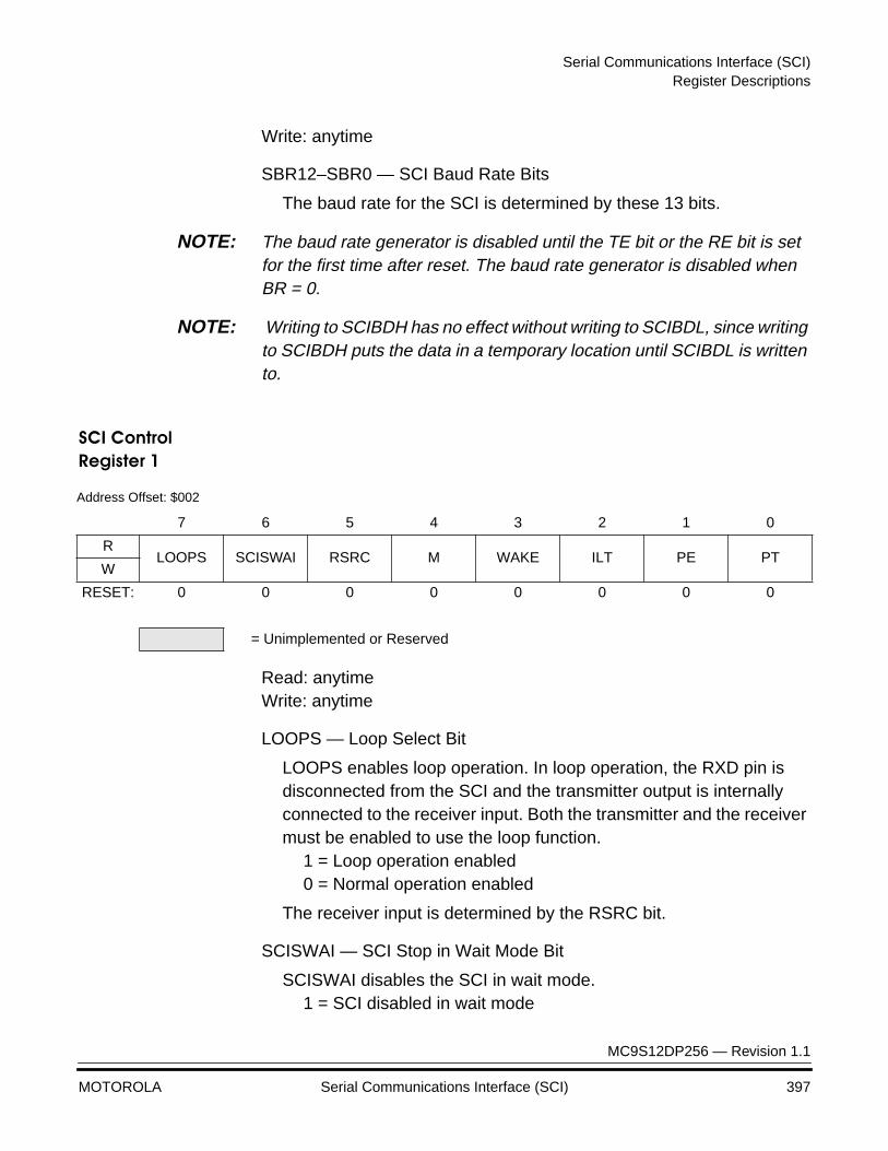
Serial Communications Interface (SCI)Register Descriptions
MC9S12DP256 — Revision 1.1
MOTOROLA Serial Communications Interface (SCI) 397
Write: anytime
SBR12–SBR0 — SCI Baud Rate Bits
The baud rate for the SCI is determined by these 13 bits.
NOTE: The baud rate generator is disabled until the TE bit or the RE bit is set for the first time after reset. The baud rate generator is disabled when BR = 0.
NOTE: Writing to SCIBDH has no effect without writing to SCIBDL, since writing to SCIBDH puts the data in a temporary location until SCIBDL is written to.
SCI Control Register 1
Read: anytimeWrite: anytime
LOOPS — Loop Select Bit
LOOPS enables loop operation. In loop operation, the RXD pin is disconnected from the SCI and the transmitter output is internally connected to the receiver input. Both the transmitter and the receiver must be enabled to use the loop function.
1 = Loop operation enabled0 = Normal operation enabled
The receiver input is determined by the RSRC bit.
SCISWAI — SCI Stop in Wait Mode Bit
SCISWAI disables the SCI in wait mode.1 = SCI disabled in wait mode
Address Offset: $002
7 6 5 4 3 2 1 0
RLOOPS SCISWAI RSRC M WAKE ILT PE PT
W
RESET: 0 0 0 0 0 0 0 0
= Unimplemented or Reserved

Serial Communications Interface (SCI)
MC9S12DP256 — Revision 1.1
398 Serial Communications Interface (SCI) MOTOROLA
0 = SCI enabled in wait mode
RSRC — Receiver Source Bit
When LOOPS = 1, the RSRC bit determines the source for the receiver shift register input.
1 = Receiver input connected externally to transmitter0 = Receiver input internally connected to transmitter output
M — Data Format Mode Bit
MODE determines whether data characters are eight or nine bits long.
1 = One start bit, nine data bits, one stop bit0 = One start bit, eight data bits, one stop bit
WAKE — Wakeup Condition Bit
WAKE determines which condition wakes up the SCI: a logic 1 (address mark) in the most significant bit position of a received data character or an idle condition on the sci_rx_ind.
1 = Address mark wakeup0 = Idle line wakeup
ILT — Idle Line Type Bit
ILT determines when the receiver starts counting logic 1s as idle character bits. The counting begins either after the start bit or after the stop bit. If the count begins after the start bit, then a string of logic 1s preceding the stop bit may cause false recognition of an idle character. Beginning the count after the stop bit avoids false idle character recognition, but requires properly synchronized transmissions.
1 = Idle character bit count begins after stop bit0 = Idle character bit count begins after start bit
Table 66 Loop Functions
LOOPS RSRC Function
0 x Normal operation
1 0 Loop mode with Rx input internally connected to Tx output
1 1 Single-wire mode with Rx input connected to sci_tx_ind
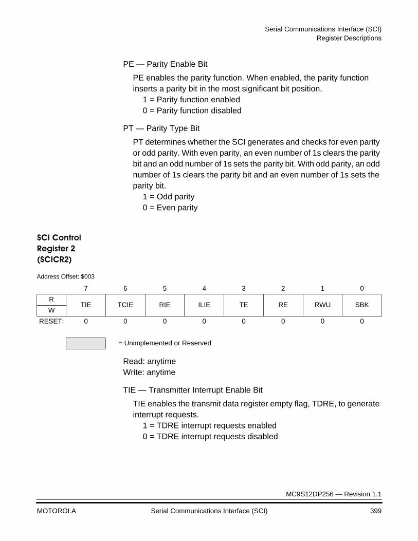
Serial Communications Interface (SCI)Register Descriptions
MC9S12DP256 — Revision 1.1
MOTOROLA Serial Communications Interface (SCI) 399
PE — Parity Enable Bit
PE enables the parity function. When enabled, the parity function inserts a parity bit in the most significant bit position.
1 = Parity function enabled0 = Parity function disabled
PT — Parity Type Bit
PT determines whether the SCI generates and checks for even parity or odd parity. With even parity, an even number of 1s clears the parity bit and an odd number of 1s sets the parity bit. With odd parity, an odd number of 1s clears the parity bit and an even number of 1s sets the parity bit.
1 = Odd parity0 = Even parity
SCI Control Register 2 (SCICR2)
Read: anytimeWrite: anytime
TIE — Transmitter Interrupt Enable Bit
TIE enables the transmit data register empty flag, TDRE, to generate interrupt requests.
1 = TDRE interrupt requests enabled0 = TDRE interrupt requests disabled
Address Offset: $003
7 6 5 4 3 2 1 0
RTIE TCIE RIE ILIE TE RE RWU SBK
W
RESET: 0 0 0 0 0 0 0 0
= Unimplemented or Reserved
Serial Communications Interface (SCI)
MC9S12DP256 — Revision 1.1
400 Serial Communications Interface (SCI) MOTOROLA
TCIE — Transmission Complete Interrupt Enable Bit
TCIE enables the transmission complete flag, TC, to generate interrupt requests.
1 = TC interrupt requests enabled0 = TC interrupt requests disabled
RIE — Receiver Full Interrupt Enable Bit
RIE enables the receive data register full flag, RDRF, or the overrun flag, OR, to generate interrupt requests.
1 = RDRF and OR interrupt requests enabled0 = RDRF and OR interrupt requests disabled
ILIE — Idle Line Interrupt Enable Bit
ILIE enables the idle line flag, IDLE, to generate interrupt requests.1 = IDLE interrupt requests enabled0 = IDLE interrupt requests disabled
TE — Transmitter Enable Bit
TE enables the SCI transmitter and configures the TXD pin as being controlled by the SCI. The TE bit can be used to queue an idle preamble.
1 = Transmitter enabled0 = Transmitter disabled
RE — Receiver Enable Bit
RE enables the SCI receiver.1 = Receiver enabled0 = Receiver disabled
RWU — Receiver Wakeup Bit
Standby state1 = Normal operation0 = RWU enables the wakeup function and inhibits further receiver
interrupt requests. Normally, hardware wakes the receiver by automatically clearing RWU.
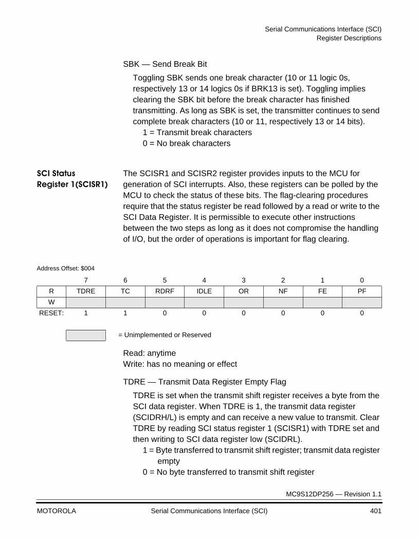
Serial Communications Interface (SCI)Register Descriptions
MC9S12DP256 — Revision 1.1
MOTOROLA Serial Communications Interface (SCI) 401
SBK — Send Break Bit
Toggling SBK sends one break character (10 or 11 logic 0s, respectively 13 or 14 logics 0s if BRK13 is set). Toggling implies clearing the SBK bit before the break character has finished transmitting. As long as SBK is set, the transmitter continues to send complete break characters (10 or 11, respectively 13 or 14 bits).
1 = Transmit break characters0 = No break characters
SCI Status Register 1(SCISR1)
The SCISR1 and SCISR2 register provides inputs to the MCU for generation of SCI interrupts. Also, these registers can be polled by the MCU to check the status of these bits. The flag-clearing procedures require that the status register be read followed by a read or write to the SCI Data Register. It is permissible to execute other instructions between the two steps as long as it does not compromise the handling of I/O, but the order of operations is important for flag clearing.
Read: anytimeWrite: has no meaning or effect
TDRE — Transmit Data Register Empty Flag
TDRE is set when the transmit shift register receives a byte from the SCI data register. When TDRE is 1, the transmit data register (SCIDRH/L) is empty and can receive a new value to transmit. Clear TDRE by reading SCI status register 1 (SCISR1) with TDRE set and then writing to SCI data register low (SCIDRL).
1 = Byte transferred to transmit shift register; transmit data register empty
0 = No byte transferred to transmit shift register
Address Offset: $004
7 6 5 4 3 2 1 0
R TDRE TC RDRF IDLE OR NF FE PF
W
RESET: 1 1 0 0 0 0 0 0
= Unimplemented or Reserved
Serial Communications Interface (SCI)
MC9S12DP256 — Revision 1.1
402 Serial Communications Interface (SCI) MOTOROLA
TC — Transmit Complete Flag
TC is set low when there is a transmission in progress or when a preamble or break character is loaded. TC is set high when the TDRE flag is set and no data, preamble, or break character is being transmitted. When TC is set, the sci_tx_do becomes idle (logic 1). Clear TC by reading SCI status register 1 (SCISR1) with TC set and then writing to SCI data register low (SCIDRL). TC is cleared automatically when data, preamble, or break is queued and ready to be sent. TC is cleared in the event of a simultaneous set and clear of the TC flag (transmission not complete).
1 = No transmission in progress0 = Transmission in progress
RDRF — Receive Data Register Full Flag
RDRF is set when the data in the receive shift register transfers to the SCI data register. Clear RDRF by reading SCI status register 1 (SCISR1) with RDRF set and then reading SCI data register low (SCIDRL).
1 = Received data available in SCI data register0 = Data not available in SCI data register
IDLE — Idle Line Flag
IDLE is set when 10 consecutive logic 1s (if M=0) or 11 consecutive logic 1s (if M=1) appear on the receiver input. Once the IDLE flag is cleared, a valid frame must again set the RDRF flag before an idle condition can set the IDLE flag.Clear IDLE by reading SCI status register 1 (SCISR1) with IDLE set and then reading SCI data register low (SCIDRL).
1 = Receiver input has become idle0 = Receiver input is either active now or has never become active
since the IDLE flag was last cleared
NOTE: When the receiver wakeup bit (RWU) is set, an idle line condition does not set the IDLE flag.

Serial Communications Interface (SCI)Register Descriptions
MC9S12DP256 — Revision 1.1
MOTOROLA Serial Communications Interface (SCI) 403
OR — Overrun Flag
OR is set when software fails to read the SCI data register before the receive shift register receives the next frame. The OR bit is set immediately after the stop bit has been completely received for the second frame. The data in the shift register is lost, but the data already in the SCI data registers is not affected. Clear OR by reading SCI status register 1 (SCISR1) with OR set and then reading SCI data register low (SCIDRL).
1 = Overrun0 = No overrun
NF — Noise Flag
NF is set when the SCI detects noise on the receiver input. NF bit is set during the same cycle as the RDRF flag but does not get set in the case of an overrun. Clear NF by reading SCI status register 1 (SCISR1) and then reading SCI data register low (SCIDRL).
1 = Noise0 = No noise
FE — Framing Error Flag
FE is set when a logic 0 is accepted as the stop bit. FE bit is set during the same cycle as the RDRF flag, but does not get set in the case of an overrun. FE inhibits further data reception until it is cleared. Clear FE by reading SCI status register 1 (SCISR1) with FE set and then reading the SCI data register low (SCIDRL).
1 = Framing error0 = No framing error
PF — Parity Error Flag
PF is set when the parity enable bit, PE, is set and the parity of the received data does not match its parity bit. Clear PF by reading SCI status register 1 (SCISR1), and then reading SCI data register low (SCIDRL).
1 = Parity error0 = No parity error

Serial Communications Interface (SCI)
MC9S12DP256 — Revision 1.1
404 Serial Communications Interface (SCI) MOTOROLA
SCI Status Register 2 (SCISR2)
Read: anytimeWrite: anytime; writing accesses SCI status register 2; writing to any bits except TXDIR and BRK13 has no effect
BRK13 — Break Transmit character length
This bit determines whether the transmit break character is 10 or 11 bit respectively 13 or 14 bits long. The detection of a framing error is not affected by this bit.
1 = Break character is 13 or 14 bit long0 = Break Character is 10 or 11 bit long
TXDIR — Transmitter pin data direction in Single-Wire mode.
This bit determines whether the TXD pin is going to be used as an input or output, in the Single-Wire mode of operation. This bit is only relevant in the Single-Wire mode of operation.
1 = TXD pin to be used as an output in Single-Wire mode0 = TXD pin to be used as an input in Single-Wire mode
RAF — Receiver Active Flag
RAF is set when the receiver detects a logic 0 during the RT1 time period of the start bit search. RAF is cleared when the receiver detects an idle character.
1 = Reception in progress0 = No reception in progress
Address Offset: $005
7 6 5 4 3 2 1 0
R 0 0 0 0 0BRK13 TXDIR
RAF
W
RESET: 0 0 0 0 0 0 0 0
= Unimplemented or Reserved
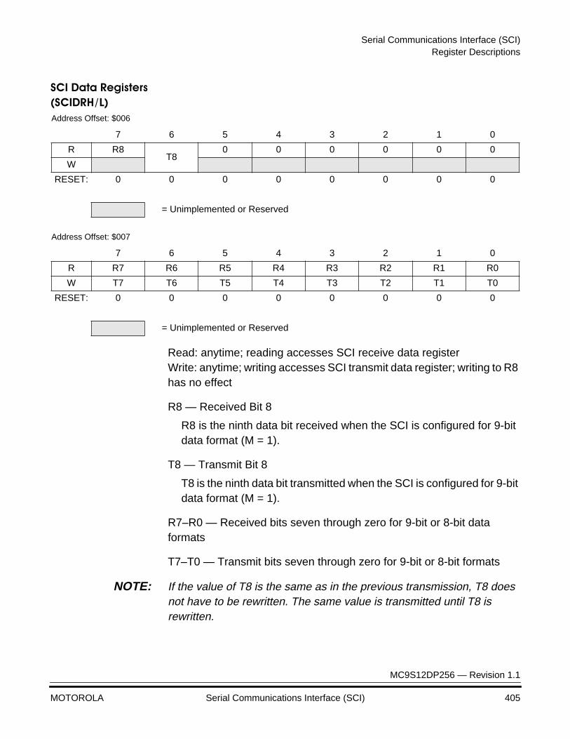
Serial Communications Interface (SCI)Register Descriptions
MC9S12DP256 — Revision 1.1
MOTOROLA Serial Communications Interface (SCI) 405
SCI Data Registers (SCIDRH/L)
Read: anytime; reading accesses SCI receive data registerWrite: anytime; writing accesses SCI transmit data register; writing to R8 has no effect
R8 — Received Bit 8
R8 is the ninth data bit received when the SCI is configured for 9-bit data format (M = 1).
T8 — Transmit Bit 8
T8 is the ninth data bit transmitted when the SCI is configured for 9-bit data format (M = 1).
R7–R0 — Received bits seven through zero for 9-bit or 8-bit data formats
T7–T0 — Transmit bits seven through zero for 9-bit or 8-bit formats
NOTE: If the value of T8 is the same as in the previous transmission, T8 does not have to be rewritten. The same value is transmitted until T8 is rewritten.
Address Offset: $006
7 6 5 4 3 2 1 0
R R8T8
0 0 0 0 0 0
W
RESET: 0 0 0 0 0 0 0 0
= Unimplemented or Reserved
Address Offset: $007
7 6 5 4 3 2 1 0
R R7 R6 R5 R4 R3 R2 R1 R0
W T7 T6 T5 T4 T3 T2 T1 T0
RESET: 0 0 0 0 0 0 0 0
= Unimplemented or Reserved
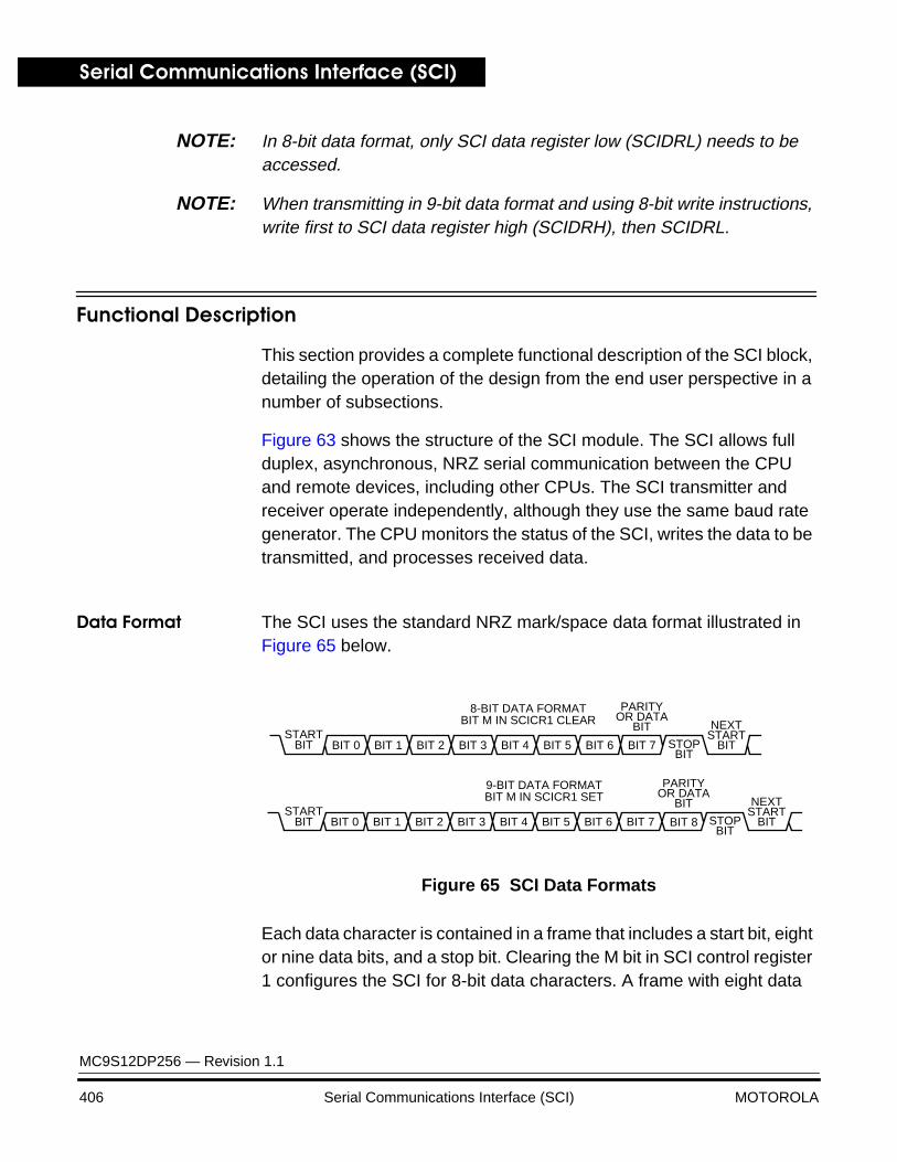
Serial Communications Interface (SCI)
MC9S12DP256 — Revision 1.1
406 Serial Communications Interface (SCI) MOTOROLA
NOTE: In 8-bit data format, only SCI data register low (SCIDRL) needs to be accessed.
NOTE: When transmitting in 9-bit data format and using 8-bit write instructions, write first to SCI data register high (SCIDRH), then SCIDRL.
Functional Description
This section provides a complete functional description of the SCI block, detailing the operation of the design from the end user perspective in a number of subsections.
Figure 63 shows the structure of the SCI module. The SCI allows full duplex, asynchronous, NRZ serial communication between the CPU and remote devices, including other CPUs. The SCI transmitter and receiver operate independently, although they use the same baud rate generator. The CPU monitors the status of the SCI, writes the data to be transmitted, and processes received data.
Data Format The SCI uses the standard NRZ mark/space data format illustrated in Figure 65 below.
Figure 65 SCI Data Formats
Each data character is contained in a frame that includes a start bit, eight or nine data bits, and a stop bit. Clearing the M bit in SCI control register 1 configures the SCI for 8-bit data characters. A frame with eight data
BIT 5START
BIT BIT 0 BIT 1
NEXT
STOPBIT
STARTBIT
9-BIT DATA FORMAT
BIT 2 BIT 3 BIT 4 BIT 6 BIT 7
PARITYOR DATA
BIT
PARITYOR DATA
BIT
BIT M IN SCICR1 SET
8-BIT DATA FORMATBIT M IN SCICR1 CLEAR
BIT 5BIT 0 BIT 1 BIT 2 BIT 3 BIT 4 BIT 6 BIT 7 BIT 8 STOPBIT
NEXTSTART
BITSTART
BIT
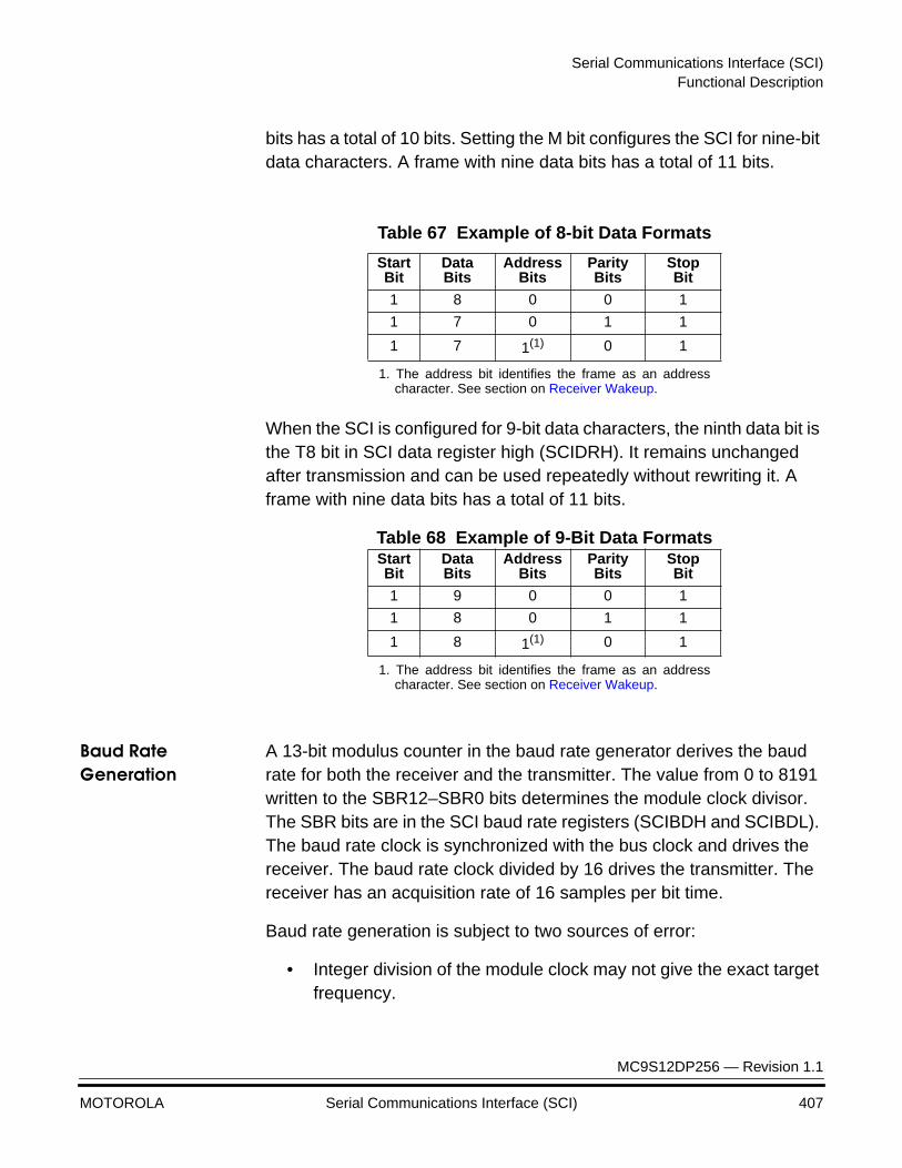
Serial Communications Interface (SCI)Functional Description
MC9S12DP256 — Revision 1.1
MOTOROLA Serial Communications Interface (SCI) 407
bits has a total of 10 bits. Setting the M bit configures the SCI for nine-bit data characters. A frame with nine data bits has a total of 11 bits.
When the SCI is configured for 9-bit data characters, the ninth data bit is the T8 bit in SCI data register high (SCIDRH). It remains unchanged after transmission and can be used repeatedly without rewriting it. A frame with nine data bits has a total of 11 bits.
Table 68 Example of 9-Bit Data Formats
Baud Rate Generation
A 13-bit modulus counter in the baud rate generator derives the baud rate for both the receiver and the transmitter. The value from 0 to 8191 written to the SBR12–SBR0 bits determines the module clock divisor. The SBR bits are in the SCI baud rate registers (SCIBDH and SCIBDL). The baud rate clock is synchronized with the bus clock and drives the receiver. The baud rate clock divided by 16 drives the transmitter. The receiver has an acquisition rate of 16 samples per bit time.
Baud rate generation is subject to two sources of error:
• Integer division of the module clock may not give the exact target frequency.
Table 67 Example of 8-bit Data Formats
StartBit
DataBits
AddressBits
ParityBits
StopBit
1 8 0 0 1
1 7 0 1 1
1 7 1(1)
1. The address bit identifies the frame as an addresscharacter. See section on Receiver Wakeup.
0 1
StartBit
DataBits
AddressBits
ParityBits
StopBit
1 9 0 0 1
1 8 0 1 1
1 8 1(1)
1. The address bit identifies the frame as an addresscharacter. See section on Receiver Wakeup.
0 1
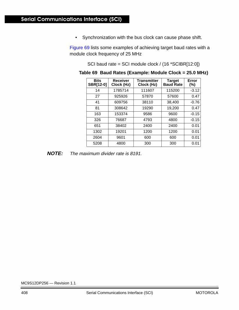
Serial Communications Interface (SCI)
MC9S12DP256 — Revision 1.1
408 Serial Communications Interface (SCI) MOTOROLA
• Synchronization with the bus clock can cause phase shift.
Figure 69 lists some examples of achieving target baud rates with a module clock frequency of 25 MHz
SCI baud rate = SCI module clock / (16 *SCIBR[12:0])
NOTE: The maximum divider rate is 8191.
Table 69 Baud Rates (Example: Module Clock = 25.0 MHz)
BitsSBR[12-0]
ReceiverClock (Hz)
TransmitterClock (Hz)
Target Baud Rate
Error (%)
14 1785714 111607 115200 -3.12
27 925926 57870 57600 0.47
41 609756 38110 38,400 -0.76
81 308642 19290 19,200 0.47
163 153374 9586 9600 -0.15
326 76687 4793 4800 -0.15
651 38402 2400 2400 0.01
1302 19201 1200 1200 0.01
2604 9601 600 600 0.01
5208 4800 300 300 0.01

Serial Communications Interface (SCI)Functional Description
MC9S12DP256 — Revision 1.1
MOTOROLA Serial Communications Interface (SCI) 409
Transmitter
Figure 66 Transmitter Block Diagram
Transmitter Character Length
The SCI transmitter can accommodate either 8-bit or 9-bit data characters. The state of the M bit in SCI control register 1 (SCICR1) determines the length of data characters. When transmitting 9-bit data, bit T8 in SCI data register high (SCIDRH) is the ninth bit (bit 8).
Character Transmission
To transmit data, the MCU writes the data bits to the SCI data registers (SCIDRH/SCIDRL), which in turn are transferred to the transmitter shift register. The transmit shift register then shifts a frame out through the sci_tx_do signal, after it has prefaced it with a start bit and appended it
PE
PT
H 8 7 6 5 4 3 2 1 0 L
11-BIT TRANSMIT SHIFT REGISTERST
OP
ST
AR
T
T8
TDRE
TIE
TCIE
SBK
TC
PARITYGENERATION
MS
B
SCI DATA REGISTERS
LOA
D F
RO
M S
CID
R
SH
IFT
EN
AB
LE
PR
EA
MB
LE (A
LL O
NE
S)
BR
EA
K (
ALL
0s)
TRANSMITTER CONTROL
M
INTERNAL BUS
SBR12–SBR0
BAUD DIVIDER ÷ 16
TDRE INTERRUPT REQUEST
TC INTERRUPT REQUEST
MODULE
LOOP
RSRC
CLOCK
TE
TOCONTROL RECEIVER
sci_tx_port_en
LOOPS
sci_tx_do
sci_tx_obe
BRK13
Serial Communications Interface (SCI)
MC9S12DP256 — Revision 1.1
410 Serial Communications Interface (SCI) MOTOROLA
with a stop bit. The SCI data registers (SCIDRH and SCIDRL) are the write-only buffers between the internal data bus and the transmit shift register.
The SCI also sets a flag, the transmit data register empty flag (TDRE), every time it transfers data from the buffer (SCIDRH/L) to the transmitter shift register.The transmit driver routine may respond to this flag by writing another byte to the Transmitter buffer (SCIDRH/SCIDRL), while the shift register is still shifting out the first byte.
To initiate an SCI transmission:
4. Configure the SCI:
a. Select a baud rate. Write this value to the SCI baud registers (SCIBDH/L) to begin the baud rate generator. Remember that the baud rate generator is disabled when the baud rate is zero. Writing to the SCIBDH has no effect without also writing to SCIBDL.
b. Write to SCICR1 to configure word length, parity, and other configuration bits (LOOPS, RSRC, M, WAKE, ILT, PE, PT).
c. Enable the transmitter, interrupts, receive, and wake up as required, by writing to the SCICR2 register bits (TIE, TCIE, RIE, ILIE, TE, RE, RWU, SBK). A preamble or idle character will now be shifted out of the transmitter shift register.
5. Transmit Procedure for Each Byte:
a. Poll the TDRE flag by reading the SCISR1 or responding to the TDRE interrupt. Keep in mind that the TDRE bit resets to one.
b. If the TDRE flag is set, write the data to be transmitted to SCIDRH/L, where the ninth bit is written to the T8 bit in SCIDRH if the SCI is in 9-bit data format. A new transmission will not result until the TDRE flag has been cleared.
6. Repeat step 2 for each subsequent transmission.
NOTE: The TDRE flag is set when the shift register is loaded with the next data to be transmitted from SCIDRH/L, which happens, generally speaking, a little over half-way through the stop bit of the previous frame.
Serial Communications Interface (SCI)Functional Description
MC9S12DP256 — Revision 1.1
MOTOROLA Serial Communications Interface (SCI) 411
Specifically, this transfer occurs 9/16ths of a bit time AFTER the start of the stop bit of the previous frame.
Writing the TE bit from 0 to a 1 automatically loads the transmit shift register with a preamble of 10 logic 1s (if M = 0) or 11 logic 1s (if M = 1). After the preamble shifts out, control logic transfers the data from the SCI data register into the transmit shift register. A logic 0 start bit automatically goes into the least significant bit position of the transmit shift register. A logic 1 stop bit goes into the most significant bit position.
Hardware supports odd or even parity. When parity is enabled, the most significant bit (msb) of the data character is the parity bit.
The transmit data register empty flag, TDRE, in SCI status register 1 (SCISR1) becomes set when the SCI data register transfers a byte to the transmit shift register. The TDRE flag indicates that the SCI data register can accept new data from the internal data bus. If the transmit interrupt enable bit, TIE, in SCI control register 2 (SCICR2) is also set, the TDRE flag generates a transmitter interrupt request.
When the transmit shift register is not transmitting a frame, the sci_tx_do signal goes to the idle condition, logic 1. If at any time software clears the TE bit in SCI control register 2 (SCICR2), the transmitter enable signal goes low and the transmit signal goes idle.
If software clears TE while a transmission is in progress (TC = 0), the frame in the transmit shift register continues to shift out. Then the sci_tx_port_en signal is de-asserted and the sci_tx_do signal goes idle even if there is data pending in the SCI data register. To avoid accidentally cutting off the last frame in a message, always wait for TDRE to go high after the last frame before clearing TE.
To separate messages with preambles of minimum idle line time, use this sequence between messages:
1. Write the last byte of the first message to SCIDRH/L.
2. Wait for the TDRE flag to go high, indicating the transfer of the last frame to the transmit shift register.
3. Queue a preamble by clearing and then setting the TE bit.
4. Write the first byte of the second message to SCIDRH/L.
Serial Communications Interface (SCI)
MC9S12DP256 — Revision 1.1
412 Serial Communications Interface (SCI) MOTOROLA
Break Characters Writing a logic 1 to the send break bit, SBK, in SCI control register 2 (SCICR2) loads the transmit shift register with a break character. A break character contains all logic 0s and has no start, stop, or parity bit. Break character length depends on the M bit in SCI control register 1 (SCICR1). As long as SBK is at logic 1, transmitter logic continuously loads break characters into the transmit shift register. After software clears the SBK bit, the shift register finishes transmitting the last break character and then transmits at least one logic 1. The automatic logic 1 at the end of a break character guarantees the recognition of the start bit of the next frame.
The SCI recognizes a break character when a start bit is followed by eight or nine logic 0 data bits and a logic 0 where the stop bit should be. Receiving a break character has these effects on SCI registers:
• Sets the framing error flag, FE
• Sets the receive data register full flag, RDRF
• Clears the SCI data registers (SCIDRH/L)
• May set the overrun flag, OR, noise flag, NF, parity error flag, PE, or the receiver active flag, RAF (see SCI Status Register 1(SCISR1) and SCI Status Register 2 (SCISR2))
Idle Characters An idle character contains all logic 1s and has no start, stop, or parity bit. Idle character length depends on the M bit in SCI control register 1 (SCICR1). The preamble is a synchronizing idle character that begins the first transmission initiated after writing the TE bit from 0 to 1.
If the TE bit is cleared during a transmission, the sci_tx_do signal becomes idle after completion of the transmission in progress. Clearing and then setting the TE bit during a transmission queues an idle character to be sent after the frame currently being transmitted.
NOTE: When queueing an idle character, return the TE bit to logic 1 before the stop bit of the current frame shifts out through the sci_tx_do signal. Setting TE after the stop bit appears on sci_tx_do causes data previously written to the SCI data register to be lost. Toggle the TE bit for a queued idle character while the TDRE flag is set and immediately before writing the next byte to the SCI data register.

Serial Communications Interface (SCI)Functional Description
MC9S12DP256 — Revision 1.1
MOTOROLA Serial Communications Interface (SCI) 413
NOTE: If the TE bit is clear and the transmission is complete, the SCI is not the master of the TXD pin.
Receiver
Figure 67 SCI Receiver Block Diagram
Receiver Character Length
The SCI receiver can accommodate either 8-bit or 9-bit data characters. The state of the M bit in SCI control register 1 (SCICR1) determines the length of data characters. When receiving 9-bit data, bit R8 in SCI data register high (SCIDRH) is the ninth bit (bit 8).
ALL
ON
ES
M
WAKE
ILT
PE
PT
RE
H 8 7 6 5 4 3 2 1 0 L
11-BIT RECEIVE SHIFT REGISTERST
OP
ST
AR
T
DATA
WAKEUP
PARITYCHECKING
MS
B
SCI DATA REGISTER
R8
RIE
ILIE
RWU
RDRF
OR
NF
FE
PE
INTERNAL BUS
MODULE
IDLE INTERRUPT REQUEST
RDRF/OR INTERRUPT REQUEST
SBR12–SBR0
BAUD DIVIDER
LOOP
RSRC
FROM sci_tx_ind OR TRANSMITTER
CLOCK
IDLE
RAF
RECOVERY
CONTROL
LOGIC
LOOPS
sci_rx_ind
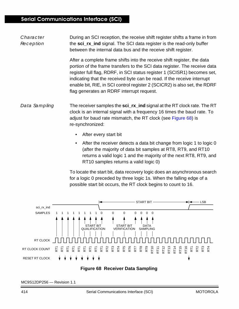
Serial Communications Interface (SCI)
MC9S12DP256 — Revision 1.1
414 Serial Communications Interface (SCI) MOTOROLA
Character Reception
During an SCI reception, the receive shift register shifts a frame in from the sci_rx_ind signal. The SCI data register is the read-only buffer between the internal data bus and the receive shift register.
After a complete frame shifts into the receive shift register, the data portion of the frame transfers to the SCI data register. The receive data register full flag, RDRF, in SCI status register 1 (SCISR1) becomes set, indicating that the received byte can be read. If the receive interrupt enable bit, RIE, in SCI control register 2 (SCICR2) is also set, the RDRF flag generates an RDRF interrupt request.
Data Sampling The receiver samples the sci_rx_ind signal at the RT clock rate. The RT clock is an internal signal with a frequency 16 times the baud rate. To adjust for baud rate mismatch, the RT clock (see Figure 68) is re-synchronized:
• After every start bit
• After the receiver detects a data bit change from logic 1 to logic 0 (after the majority of data bit samples at RT8, RT9, and RT10 returns a valid logic 1 and the majority of the next RT8, RT9, and RT10 samples returns a valid logic 0)
To locate the start bit, data recovery logic does an asynchronous search for a logic 0 preceded by three logic 1s. When the falling edge of a possible start bit occurs, the RT clock begins to count to 16.
Figure 68 Receiver Data Sampling
RESET RT CLOCK
RT
1
RT
1
RT
1
RT
1
RT
1
RT
1
RT
1
RT
1
RT
1
RT
2
RT
3
RT
4
RT
5
RT
8
RT
7
RT
6
RT
11
RT
10
RT
9
RT
15
RT
14
RT
13
RT
12
RT
16
RT
1
RT
2
RT
3
RT
4
SAMPLES
RT CLOCK
RT CLOCK COUNT
START BIT
sci_rx_ind
START BITQUALIFICATION
START BIT DATASAMPLING
1 111111 1 0 0 0 000 0
LSB
VERIFICATION
Serial Communications Interface (SCI)Functional Description
MC9S12DP256 — Revision 1.1
MOTOROLA Serial Communications Interface (SCI) 415
To verify the start bit and to detect noise, data recovery logic takes samples at RT3, RT5, and RT7. Figure 70 summarizes the results of the start bit verification samples.
If start bit verification is not successful, the RT clock is reset and a new search for a start bit begins.
To determine the value of a data bit and to detect noise, recovery logic takes samples at RT8, RT9, and RT10. Figure 71 summarizes the results of the data bit samples.
Table 71 Data Bit Recovery
NOTE: The RT8, RT9, and RT10 samples do not affect start bit verification. If any or all of the RT8, RT9, and RT10 start bit samples are logic 1s following a successful start bit verification, the noise flag (NF) is set and the receiver assumes that the bit is a start bit (logic 0).
To verify a stop bit and to detect noise, recovery logic takes samples at RT8, RT9, and RT10. Figure 72 summarizes the results of the stop bit samples.
Table 70 Start Bit Verification
RT3, RT5, and RT7 Samples Start Bit Verification Noise Flag
000 Yes 0
001 Yes 1
010 Yes 1
011 No 0
100 Yes 1
101 No 0
110 No 0
111 No 0
RT8, RT9, and RT10 Samples Data Bit Determination Noise Flag
000 0 0
001 0 1
010 0 1
011 1 1
100 0 1
101 1 1
110 1 1
111 1 0
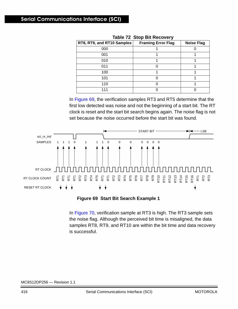
Serial Communications Interface (SCI)
MC9S12DP256 — Revision 1.1
416 Serial Communications Interface (SCI) MOTOROLA
Table 72 Stop Bit Recovery
In Figure 69, the verification samples RT3 and RT5 determine that the first low detected was noise and not the beginning of a start bit. The RT clock is reset and the start bit search begins again. The noise flag is not set because the noise occurred before the start bit was found.
Figure 69 Start Bit Search Example 1
In Figure 70, verification sample at RT3 is high. The RT3 sample sets the noise flag. Although the perceived bit time is misaligned, the data samples RT8, RT9, and RT10 are within the bit time and data recovery is successful.
RT8, RT9, and RT10 Samples Framing Error Flag Noise Flag
000 1 0
001 1 1
010 1 1
011 0 1
100 1 1
101 0 1
110 0 1
111 0 0
RESET RT CLOCK
RT
1
RT
1
RT
1
RT
1
RT
2
RT
3
RT
4
RT
5
RT
1
RT
1
RT
2
RT
3
RT
4
RT
7
RT
6
RT
5
RT
10
RT
9
RT
8
RT
14
RT
13
RT
12
RT
11
RT
15
RT
16
RT
1
RT
2
RT
3
SAMPLES
RT CLOCK
RT CLOCK COUNT
START BIT
sci_rx_ind
1 1011 1 1 0 0 00 0
LSB
0 0
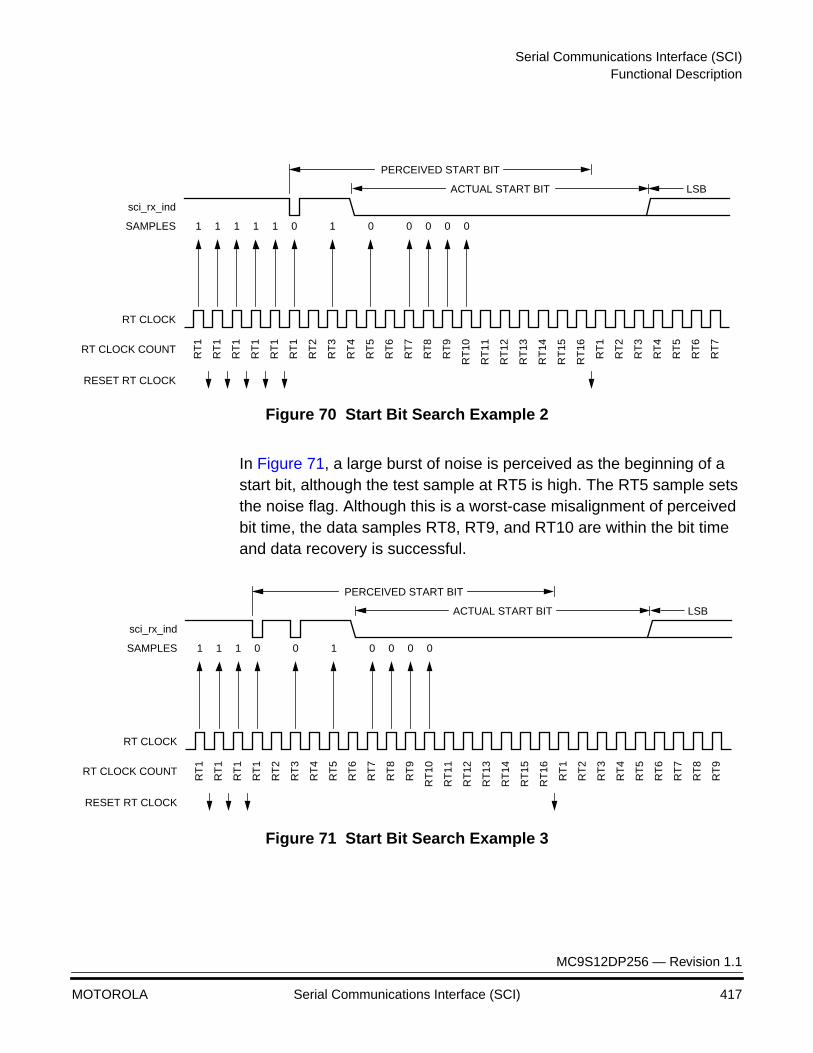
Serial Communications Interface (SCI)Functional Description
MC9S12DP256 — Revision 1.1
MOTOROLA Serial Communications Interface (SCI) 417
Figure 70 Start Bit Search Example 2
In Figure 71, a large burst of noise is perceived as the beginning of a start bit, although the test sample at RT5 is high. The RT5 sample sets the noise flag. Although this is a worst-case misalignment of perceived bit time, the data samples RT8, RT9, and RT10 are within the bit time and data recovery is successful.
Figure 71 Start Bit Search Example 3
RESET RT CLOCK
RT
1
RT
1
RT
1
RT
1
RT
1
RT
1
RT
2
RT
3
RT
4
RT
5
RT
6
RT
7
RT
8
RT
11
RT
10
RT
9
RT
14
RT
13
RT
12
RT
2
RT
1
RT
16
RT
15
RT
3
RT
4
RT
5
RT
6
RT
7
SAMPLES
RT CLOCK
RT CLOCK COUNT
ACTUAL START BIT
sci_rx_ind
1 1111 1 0 0 00
LSB
00
PERCEIVED START BIT
RESET RT CLOCK
RT
1
RT
1
RT
1
RT
1
RT
2
RT
3
RT
4
RT
5
RT
6
RT
7
RT
8
RT
9
RT
10
RT
13
RT
12
RT
11
RT
16
RT
15
RT
14
RT
4
RT
3
RT
2
RT
1
RT
5
RT
6
RT
7
RT
8
RT
9
SAMPLES
RT CLOCK
RT CLOCK COUNT
ACTUAL START BIT
sci_rx_ind
1 011 1 0 0 00
LSB
0
PERCEIVED START BIT
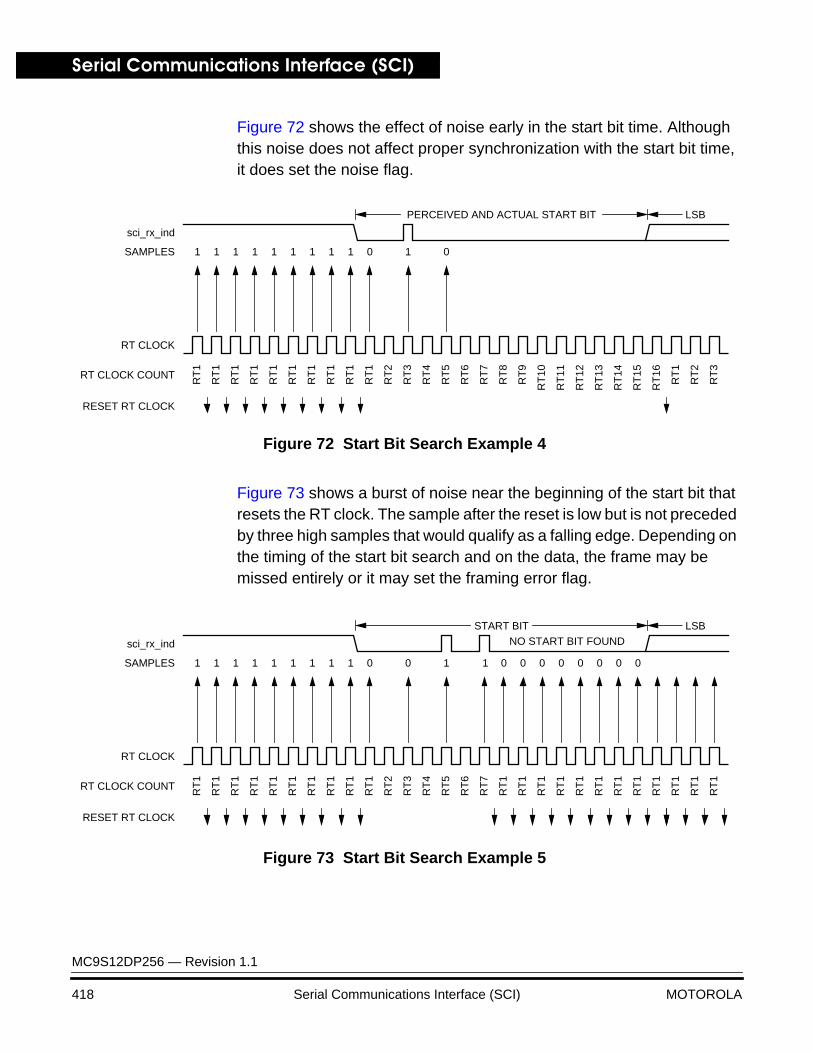
Serial Communications Interface (SCI)
MC9S12DP256 — Revision 1.1
418 Serial Communications Interface (SCI) MOTOROLA
Figure 72 shows the effect of noise early in the start bit time. Although this noise does not affect proper synchronization with the start bit time, it does set the noise flag.
Figure 72 Start Bit Search Example 4
Figure 73 shows a burst of noise near the beginning of the start bit that resets the RT clock. The sample after the reset is low but is not preceded by three high samples that would qualify as a falling edge. Depending on the timing of the start bit search and on the data, the frame may be missed entirely or it may set the framing error flag.
Figure 73 Start Bit Search Example 5
RESET RT CLOCK
RT
1
RT
1
RT
1
RT
1
RT
1
RT
1
RT
1
RT
1
RT
1
RT
1
RT
2
RT
3
RT
4
RT
7
RT
6
RT
5
RT
10
RT
9
RT
8
RT
14
RT
13
RT
12
RT
11
RT
15
RT
16
RT
1
RT
2
RT
3
SAMPLES
RT CLOCK
RT CLOCK COUNT
PERCEIVED AND ACTUAL START BIT
sci_rx_ind
1 111 1 0 01
LSB
11 1 1
RESET RT CLOCK
RT
1
RT
1
RT
1
RT
1
RT
1
RT
1
RT
1
RT
1
RT
1
RT
1
RT
2
RT
3
RT
4
RT
7
RT
6
RT
5
RT
1
RT
1
RT
1
RT
1
RT
1
RT
1
RT
1
RT
1
RT
1
RT
1
RT
1
RT
1
SAMPLES
RT CLOCK
RT CLOCK COUNT
START BIT
sci_rx_ind
1 111 1 0 10
LSB
11 1 1 1 0 000 000 0
NO START BIT FOUND
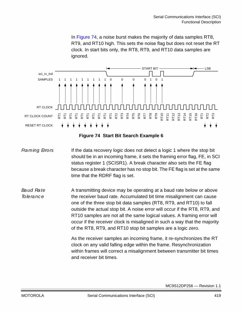
Serial Communications Interface (SCI)Functional Description
MC9S12DP256 — Revision 1.1
MOTOROLA Serial Communications Interface (SCI) 419
In Figure 74, a noise burst makes the majority of data samples RT8, RT9, and RT10 high. This sets the noise flag but does not reset the RT clock. In start bits only, the RT8, RT9, and RT10 data samples are ignored.
Figure 74 Start Bit Search Example 6
Framing Errors If the data recovery logic does not detect a logic 1 where the stop bit should be in an incoming frame, it sets the framing error flag, FE, in SCI status register 1 (SCISR1). A break character also sets the FE flag because a break character has no stop bit. The FE flag is set at the same time that the RDRF flag is set.
Baud Rate Tolerance
A transmitting device may be operating at a baud rate below or above the receiver baud rate. Accumulated bit time misalignment can cause one of the three stop bit data samples (RT8, RT9, and RT10) to fall outside the actual stop bit. A noise error will occur if the RT8, RT9, and RT10 samples are not all the same logical values. A framing error will occur if the receiver clock is misaligned in such a way that the majority of the RT8, RT9, and RT10 stop bit samples are a logic zero.
As the receiver samples an incoming frame, it re-synchronizes the RT clock on any valid falling edge within the frame. Resynchronization within frames will correct a misalignment between transmitter bit times and receiver bit times.
RESET RT CLOCK
RT
1
RT
1
RT
1
RT
1
RT
1
RT
1
RT
1
RT
1
RT
1
RT
1
RT
2
RT
3
RT
4
RT
7
RT
6
RT
5
RT
10
RT
9
RT
8
RT
14
RT
13
RT
12
RT
11
RT
15
RT
16
RT
1
RT
2
RT
3
SAMPLES
RT CLOCK
RT CLOCK COUNT
START BIT
sci_rx_ind
1 111 1 0 00
LSB
11 1 1 0 1 10
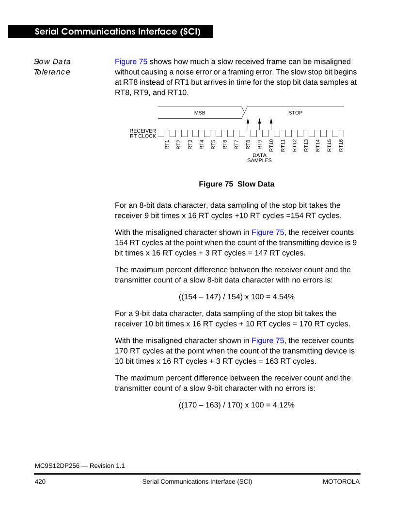
Serial Communications Interface (SCI)
MC9S12DP256 — Revision 1.1
420 Serial Communications Interface (SCI) MOTOROLA
Slow Data Tolerance
Figure 75 shows how much a slow received frame can be misaligned without causing a noise error or a framing error. The slow stop bit begins at RT8 instead of RT1 but arrives in time for the stop bit data samples at RT8, RT9, and RT10.
Figure 75 Slow Data
For an 8-bit data character, data sampling of the stop bit takes the receiver 9 bit times x 16 RT cycles +10 RT cycles =154 RT cycles.
With the misaligned character shown in Figure 75, the receiver counts 154 RT cycles at the point when the count of the transmitting device is 9 bit times x 16 RT cycles + 3 RT cycles = 147 RT cycles.
The maximum percent difference between the receiver count and the transmitter count of a slow 8-bit data character with no errors is:
((154 – 147) / 154) x 100 = 4.54%
For a 9-bit data character, data sampling of the stop bit takes the receiver 10 bit times x 16 RT cycles + 10 RT cycles = 170 RT cycles.
With the misaligned character shown in Figure 75, the receiver counts 170 RT cycles at the point when the count of the transmitting device is 10 bit times x 16 RT cycles + 3 RT cycles = 163 RT cycles.
The maximum percent difference between the receiver count and the transmitter count of a slow 9-bit character with no errors is:
((170 – 163) / 170) x 100 = 4.12%
MSB STOP
RT
1
RT
2
RT
3
RT
4
RT
5
RT
6
RT
7
RT
8
RT
9
RT
10
RT
11
RT
12
RT
13
RT
14
RT
15
RT
16
DATASAMPLES
RECEIVERRT CLOCK
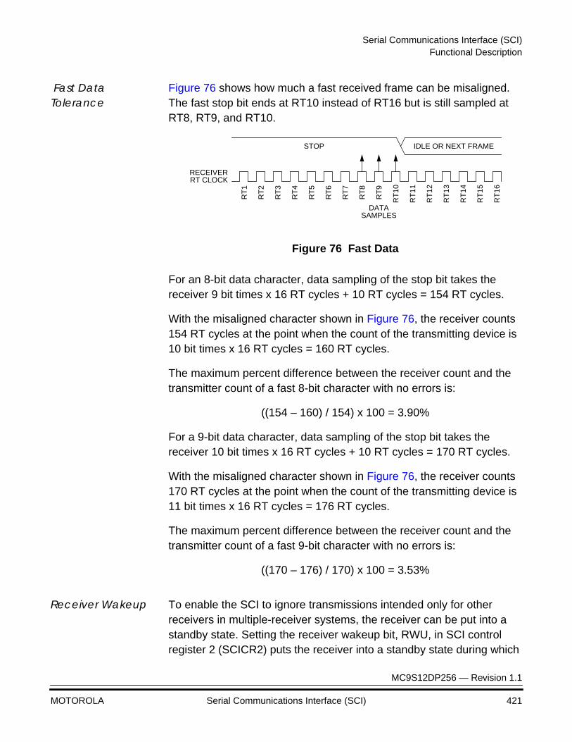
Serial Communications Interface (SCI)Functional Description
MC9S12DP256 — Revision 1.1
MOTOROLA Serial Communications Interface (SCI) 421
Fast Data Tolerance
Figure 76 shows how much a fast received frame can be misaligned. The fast stop bit ends at RT10 instead of RT16 but is still sampled at RT8, RT9, and RT10.
Figure 76 Fast Data
For an 8-bit data character, data sampling of the stop bit takes the receiver 9 bit times x 16 RT cycles + 10 RT cycles = 154 RT cycles.
With the misaligned character shown in Figure 76, the receiver counts 154 RT cycles at the point when the count of the transmitting device is 10 bit times x 16 RT cycles = 160 RT cycles.
The maximum percent difference between the receiver count and the transmitter count of a fast 8-bit character with no errors is:
((154 – 160) / 154) x 100 = 3.90%
For a 9-bit data character, data sampling of the stop bit takes the receiver 10 bit times x 16 RT cycles + 10 RT cycles = 170 RT cycles.
With the misaligned character shown in Figure 76, the receiver counts 170 RT cycles at the point when the count of the transmitting device is 11 bit times x 16 RT cycles = 176 RT cycles.
The maximum percent difference between the receiver count and the transmitter count of a fast 9-bit character with no errors is:
((170 – 176) / 170) x 100 = 3.53%
Receiver Wakeup To enable the SCI to ignore transmissions intended only for other receivers in multiple-receiver systems, the receiver can be put into a standby state. Setting the receiver wakeup bit, RWU, in SCI control register 2 (SCICR2) puts the receiver into a standby state during which
IDLE OR NEXT FRAMESTOP
RT
1
RT
2
RT
3
RT
4
RT
5
RT
6
RT
7
RT
8
RT
9
RT
10
RT
11
RT
12
RT
13
RT
14
RT
15
RT
16
DATASAMPLES
RECEIVERRT CLOCK
Serial Communications Interface (SCI)
MC9S12DP256 — Revision 1.1
422 Serial Communications Interface (SCI) MOTOROLA
receiver interrupts are disabled.The SCI will still load the receive data into the SCIDRH/L registers, but it will not set the RDRF flag.
The transmitting device can address messages to selected receivers by including addressing information in the initial frame or frames of each message.
The WAKE bit in SCI control register 1 (SCICR1) determines how the SCI is brought out of the standby state to process an incoming message. The WAKE bit enables either idle line wakeup or address mark wakeup.
Idle input line wakeup (WAKE = 0)
In this wakeup method, an idle condition on the sci_rx_ind signal clears the RWU bit and wakes up the SCI. The initial frame or frames of every message contain addressing information. All receivers evaluate the addressing information, and receivers for which the message is addressed process the frames that follow. Any receiver for which a message is not addressed can set its RWU bit and return to the standby state. The RWU bit remains set and the receiver remains on standby until another idle character appears on the sci_rx_ind signal.
Idle line wakeup requires that messages be separated by at least one idle character and that no message contains idle characters.
The idle character that wakes a receiver does not set the receiver idle bit, IDLE, or the receive data register full flag, RDRF.
The idle line type bit, ILT, determines whether the receiver begins counting logic 1s as idle character bits after the start bit or after the stop bit. ILT is in SCI control register 1 (SCICR1).
Address mark wakeup (WAKE = 1)
In this wakeup method, a logic 1 in the most significant bit (msb) position of a frame clears the RWU bit and wakes up the SCI. The logic 1 in the msb position marks a frame as an address frame that contains addressing information. All receivers evaluate the addressing information, and the receivers for which the message is addressed process the frames that follow. Any receiver for which a message is not addressed can set its RWU bit and return to the standby state. The RWU bit remains set and the receiver remains on standby until another address frame appears on the sci_rx_ind signal.
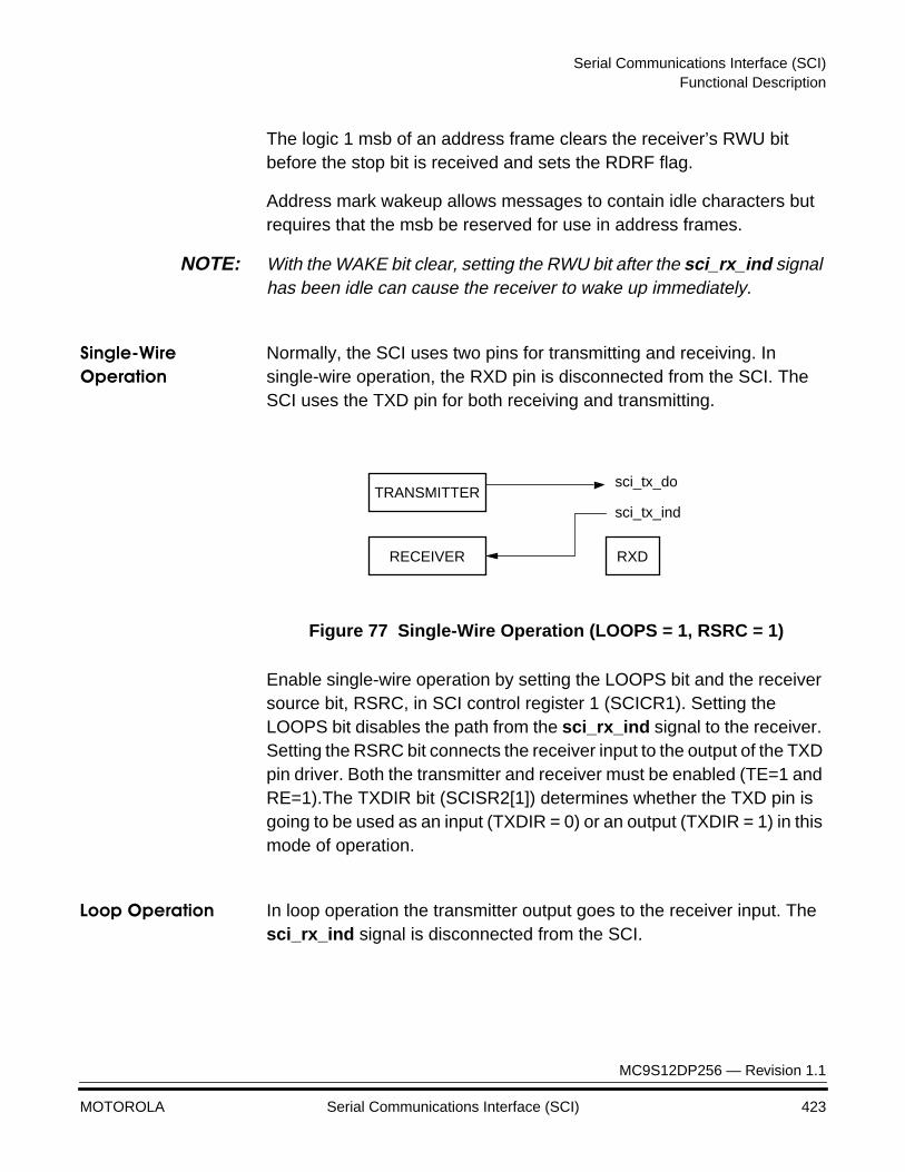
Serial Communications Interface (SCI)Functional Description
MC9S12DP256 — Revision 1.1
MOTOROLA Serial Communications Interface (SCI) 423
The logic 1 msb of an address frame clears the receiver’s RWU bit before the stop bit is received and sets the RDRF flag.
Address mark wakeup allows messages to contain idle characters but requires that the msb be reserved for use in address frames.
NOTE: With the WAKE bit clear, setting the RWU bit after the sci_rx_ind signal has been idle can cause the receiver to wake up immediately.
Single-Wire Operation
Normally, the SCI uses two pins for transmitting and receiving. In single-wire operation, the RXD pin is disconnected from the SCI. The SCI uses the TXD pin for both receiving and transmitting.
Figure 77 Single-Wire Operation (LOOPS = 1, RSRC = 1)
Enable single-wire operation by setting the LOOPS bit and the receiver source bit, RSRC, in SCI control register 1 (SCICR1). Setting the LOOPS bit disables the path from the sci_rx_ind signal to the receiver. Setting the RSRC bit connects the receiver input to the output of the TXD pin driver. Both the transmitter and receiver must be enabled (TE=1 and RE=1).The TXDIR bit (SCISR2[1]) determines whether the TXD pin is going to be used as an input (TXDIR = 0) or an output (TXDIR = 1) in this mode of operation.
Loop Operation In loop operation the transmitter output goes to the receiver input. The sci_rx_ind signal is disconnected from the SCI.
RXD
TRANSMITTER
RECEIVER
sci_tx_do
sci_tx_ind
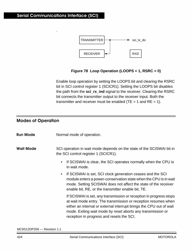
Serial Communications Interface (SCI)
MC9S12DP256 — Revision 1.1
424 Serial Communications Interface (SCI) MOTOROLA
.
Figure 78 Loop Operation (LOOPS = 1, RSRC = 0)
Enable loop operation by setting the LOOPS bit and clearing the RSRC bit in SCI control register 1 (SCICR1). Setting the LOOPS bit disables the path from the sci_rx_ind signal to the receiver. Clearing the RSRC bit connects the transmitter output to the receiver input. Both the transmitter and receiver must be enabled (TE = 1 and RE = 1).
Modes of Operation
Run Mode Normal mode of operation.
Wait Mode SCI operation in wait mode depends on the state of the SCISWAI bit in the SCI control register 1 (SCICR1).
• If SCISWAI is clear, the SCI operates normally when the CPU is in wait mode.
• If SCISWAI is set, SCI clock generation ceases and the SCI module enters a power-conservation state when the CPU is in wait mode. Setting SCISWAI does not affect the state of the receiver enable bit, RE, or the transmitter enable bit, TE.
If SCISWAI is set, any transmission or reception in progress stops at wait mode entry. The transmission or reception resumes when either an internal or external interrupt brings the CPU out of wait mode. Exiting wait mode by reset aborts any transmission or reception in progress and resets the SCI.
RXD
TRANSMITTER
RECEIVER
sci_tx_do
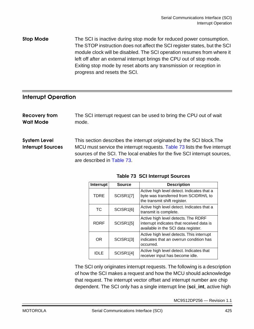
Serial Communications Interface (SCI)Interrupt Operation
MC9S12DP256 — Revision 1.1
MOTOROLA Serial Communications Interface (SCI) 425
Stop Mode The SCI is inactive during stop mode for reduced power consumption. The STOP instruction does not affect the SCI register states, but the SCI module clock will be disabled. The SCI operation resumes from where it left off after an external interrupt brings the CPU out of stop mode. Exiting stop mode by reset aborts any transmission or reception in progress and resets the SCI.
Interrupt Operation
Recovery from Wait Mode
The SCI interrupt request can be used to bring the CPU out of wait mode.
System Level Interrupt Sources
This section describes the interrupt originated by the SCI block.The MCU must service the interrupt requests. Table 73 lists the five interrupt sources of the SCI. The local enables for the five SCI interrupt sources, are described in Table 73.
The SCI only originates interrupt requests. The following is a description of how the SCI makes a request and how the MCU should acknowledge that request. The interrupt vector offset and interrupt number are chip dependent. The SCI only has a single interrupt line (sci_int, active high
Table 73 SCI Interrupt Sources
Interrupt Source Description
TDRE SCISR1[7]Active high level detect. Indicates that a byte was transferred from SCIDRH/L to the transmit shift register.
TC SCISR1[6]Active high level detect. Indicates that a transmit is complete.
RDRF SCISR1[5]Active high level detects. The RDRF interrupt indicates that received data is available in the SCI data register.
OR SCISR1[3]Active high level detects. This interrupt indicates that an overrun condition has occurred.
IDLE SCISR1[4]Active high level detect. Indicates that receiver input has become idle.
Serial Communications Interface (SCI)
MC9S12DP256 — Revision 1.1
426 Serial Communications Interface (SCI) MOTOROLA
operation) and all the following interrupts, when generated, are ORed together and issued through that port.
TDRE Description The TDRE interrupt is set high by the SCI when the transmit shift register receives a byte from the SCI data register. A TDRE interrupt indicates that the transmit shift register (SCIDRH/L) is empty and that a new byte can be written to the SCIDRH/L for transmission.Clear TDRE by reading SCI status register 1 with TDRE set and then writing to SCI data register low (SCIDRL).
TC Description The TC interrupt is set by the SCI when a transmission has been completed. A TC interrupt indicates that there is no transmission in progress. TC is set high when the TDRE flag is set and no data, preamble, or break character is being transmitted. When TC is set, the TXD pin becomes idle (logic 1). Clear TC by reading SCI status register 1 (SCISR1) with TC set and then writing to SCI data register low (SCIDRL). TC is cleared automatically when data, preamble, or break is queued and ready to be sent.
RDRF Description The RDRF interrupt is set when the data in the receive shift register transfers to the SCI data register. A RDRF interrupt indicates that the received data has been transferred to the SCI data register and that the byte can now be read by the MCU. The RDRF interrupt is cleared by reading the SCI status register one (SCISR1) and then reading SCI data register low (SCIDRL).
OR Description The OR interrupt is set when software fails to read the SCI data register before the receive shift register receives the next frame. The newly acquired data in the shift register will be lost in this case, but the data already in the SCI data registers is not affected. The OR interrupt is cleared by reading the SCI status register one (SCISR1) and then reading SCI data register low (SCIDRL).
IDLE Description The IDLE interrupt is set when 10 consecutive logic 1s (if M=0) or 11 consecutive logic 1s (if M=1) appear on the receiver input. Once the IDLE is cleared, a valid frame must again set the RDRF flag before an

Serial Communications Interface (SCI)Interrupt Operation
MC9S12DP256 — Revision 1.1
MOTOROLA Serial Communications Interface (SCI) 427
idle condition can set the IDLE flag. Clear IDLE by reading SCI status register 1 (SCISR1) with IDLE set and then reading SCI data register low (SCIDRL).

Serial Communications Interface (SCI)
MC9S12DP256 — Revision 1.1
428 Serial Communications Interface (SCI) MOTOROLA
MC9S12DP256 — Revision 1.1
MOTOROLA Serial Peripheral Interface (SPI) 429
Serial Peripheral Interface (SPI)Serial Peripheral Interface (SPI)
Contents
Overview . . . . . . . . . . . . . . . . . . . . . . . . . . . . . . . . . . . . . . . . . . . . . . 429Features . . . . . . . . . . . . . . . . . . . . . . . . . . . . . . . . . . . . . . . . . . . . . . 430Modes of Operation. . . . . . . . . . . . . . . . . . . . . . . . . . . . . . . . . . . . . . 430Block Diagram. . . . . . . . . . . . . . . . . . . . . . . . . . . . . . . . . . . . . . . . . . 431Signal Descriptions . . . . . . . . . . . . . . . . . . . . . . . . . . . . . . . . . . . . . . 432Module Memory Map . . . . . . . . . . . . . . . . . . . . . . . . . . . . . . . . . . . . 436Register Quick Reference . . . . . . . . . . . . . . . . . . . . . . . . . . . . . . . . . 437Register Descriptions . . . . . . . . . . . . . . . . . . . . . . . . . . . . . . . . . . . . 438Functional Description. . . . . . . . . . . . . . . . . . . . . . . . . . . . . . . . . . . . 446Low Power Mode Options . . . . . . . . . . . . . . . . . . . . . . . . . . . . . . . . . 457Errata . . . . . . . . . . . . . . . . . . . . . . . . . . . . . . . . . . . . . . . . . . . . . . . . 459Reset. . . . . . . . . . . . . . . . . . . . . . . . . . . . . . . . . . . . . . . . . . . . . . . . . 460Interrupts . . . . . . . . . . . . . . . . . . . . . . . . . . . . . . . . . . . . . . . . . . . . . . 460
Overview
The Serial Peripheral Interface module allows full-duplex, synchronous, serial communication between the MCU and peripheral devices. Software can poll the SPI status flags or the SPI operation can be interrupt driven
Serial Peripheral Interface (SPI)
MC9S12DP256 — Revision 1.1
430 Serial Peripheral Interface (SPI) MOTOROLA
Features
The Serial Peripheral Interface includes these distinctive features:
• Master mode and slave mode
• Bi-directional mode
• Slave select output
• Mode fault error flag with CPU interrupt capability
• Double-buffered operation
• Serial clock with programmable polarity and phase
• Control of SPI operation during wait mode
Modes of Operation
The SPI functions in three modes, run, wait, and stop.
• Run Mode
This is the basic mode of operation.
• Wait Mode
SPI operation in wait mode is a configurable low power mode. Depending on the state of internal bits, the SPI can operate normally when the CPU is in wait mode or the SPI clock generation can be turned off and the SPI module enters a power conservation state during wait mode. During wait mode, any master transmission in progress stops. Reception and transmission of a byte as slave continues so that the slave is synchronized to the master.
• Stop Mode
The SPI is inactive in stop mode for reduced power consumption. The STOP instruction does not affect or depend on SPI register states. Again, reception and transmission of a byte as slave continues to stay synchronized with the master.

Serial Peripheral Interface (SPI)Block Diagram
MC9S12DP256 — Revision 1.1
MOTOROLA Serial Peripheral Interface (SPI) 431
This is a high level description only, detailed descriptions of operating modes are contained in section Low Power Mode Options.
Block Diagram
Figure 79 is a block diagram of the Serial Peripheral Interface.
Figure 79 SPI Block Diagram
PINCONTROL
LOGIC
8-BIT SHIFT REGISTER
READ DATA BUFFER
SHIFT CONTROL LOGIC
CLOCKLOGIC
SPI CONTROL
SPI STATUS REGISTER
SPI DATA REGISTER
SP
RF
MO
DF
DIVIDER
SELECT
SPI BAUD RATE REGISTER
2 ∏4 8 16 32 64 128 ∏256
SPI
INTE
RR
UP
T
IPbus
SM
M
S
M
S
SP
R2
SP
R1
SP
R0
RE
QU
ES
T
SPIE
SP
E
MS
TR
CP
OL
CP
HA
LSBF
E
LSBFE
SPTI
E
SS
OE
SPE
CLOCK
MSTR
SPI CONTROL REGISTER 1
BAUD RATE GENERATOR
SP
PR
2
SP
PR
1
SP
PR
0
SP
TEF
spi_mosi_indspi_miso_ind
spi_ss_ind
spi_sck_ind
spi_mosi_port_enspi_miso_port_en
spi_ss_port_en
spi_sck_port_en
spi_mosi_obe
spi_ss_obe
spi_miso_obe
spi_sck_obe
spi_mosi_dospi_miso_do
spi_ss_dospi_sck_do
SPI CONTROL REGISTER 2S
PC
0
BID
IRO
E
MO
DFE
N
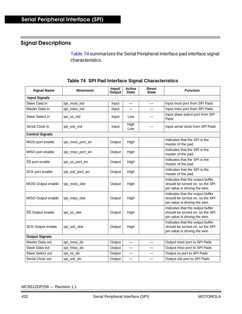
Serial Peripheral Interface (SPI)
MC9S12DP256 — Revision 1.1
432 Serial Peripheral Interface (SPI) MOTOROLA
Signal Descriptions
Table 74 summarizes the Serial Peripheral Interface pad interface signal characteristics.
Table 74 SPI Pad Interface Signal Characteristics
Signal Name Mnemonic Input/Output
ActiveState
ResetState Function
Input Signals
Slave Data in spi_mosi_ind Input — — Input mosi port from SPI Pads
Master Data in spi_miso_ind Input — — Input miso port from SPI Pads
Slave Select in spi_ss_ind Input Low —Input slave select port from SPI Pads
Serial Clock in spi_sck_ind InputHighLow
— Input serial clock from SPI Pads
Control Signals
MOSI port enable spi_mosi_port_en Output High Indicates that the SPI is the master of the pad.
MISO port enable spi_miso_port_en Output High Indicates that the SPI is the master of the pad.
SS port enable spi_ss_port_en Output High Indicates that the SPI is the master of the pad.
SCK port enable spi_sck_port_en Output High Indicates that the SPI is the master of the pad.
MOSI Output enable spi_mosi_obe Output High Indicates that the output buffer should be turned on, so the SPI pin value is driving the wire.
MISO Output enable spi_miso_obe Output High Indicates that the output buffer should be turned on, so the SPI pin value is driving the wire.
SS Output enable spi_ss_obe Output High Indicates that the output buffer should be turned on, so the SPI pin value is driving the wire.
SCK Output enable spi_sck_obe Output High Indicates that the output buffer should be turned on, so the SPI pin value is driving the wire.
Output Signals
Master Data out spi_mosi_do Output — — Output mosi port to SPI Pads
Slave Data out spi_miso_do Output — — Output miso port to SPI Pads
Slave Select out spi_ss_do Output — — Output ss port to SPI Pads
Serial Clock out spi_sck_do Output — — Output sck port to SPI Pads
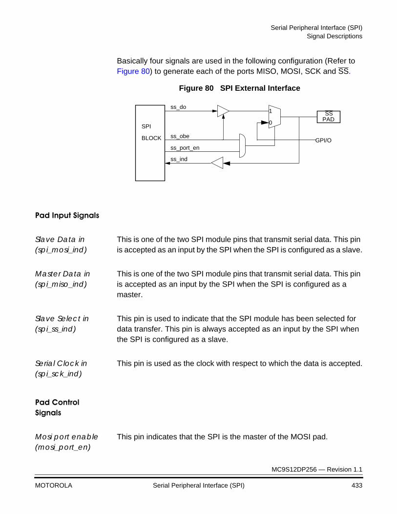
Serial Peripheral Interface (SPI)Signal Descriptions
MC9S12DP256 — Revision 1.1
MOTOROLA Serial Peripheral Interface (SPI) 433
Basically four signals are used in the following configuration (Refer to Figure 80) to generate each of the ports MISO, MOSI, SCK and SS.
Figure 80 SPI External Interface
Pad Input Signals
Slave Data in (spi_mosi_ind)
This is one of the two SPI module pins that transmit serial data. This pin is accepted as an input by the SPI when the SPI is configured as a slave.
Master Data in (spi_miso_ind)
This is one of the two SPI module pins that transmit serial data. This pin is accepted as an input by the SPI when the SPI is configured as a master.
Slave Select in (spi_ss_ind)
This pin is used to indicate that the SPI module has been selected for data transfer. This pin is always accepted as an input by the SPI when the SPI is configured as a slave.
Serial Clock in (spi_sck_ind)
This pin is used as the clock with respect to which the data is accepted.
Pad Control Signals
Mosi port enable (mosi_port_en)
This pin indicates that the SPI is the master of the MOSI pad.
ss_do
ss_obe
ss_ind
SS
SPI
BLOCK
PAD
ss_port_enGPI/O
0
1
Serial Peripheral Interface (SPI)
MC9S12DP256 — Revision 1.1
434 Serial Peripheral Interface (SPI) MOTOROLA
Normally this signal is asserted when the SPE bit of the SPICR1 register is set. Also, when configured in Slave mode and in Bidirectional mode of operation, this signal is de-asserted.
Miso port enable (miso_port_en)
This pin indicates that the SPI is the master of the MISO pad.
Normally this signal is asserted when the SPE bit of the SPICR1 register is set.Also, when configured in Master mode and in Bidirectional mode of operation, this signal is de-asserted.
SS port enable (ss_port_en)
This pin indicates that the SPI is the master of the SS pad.
Normally this signal is asserted when the SPE bit of the SPICR1 register is set. When configured in Master mode and MODFEN bit of SPICR2 is cleared, then this signal is de-asserted.
Sck port enable (sck_port_en)
This pin indicates that the SPI is the master of the SCK pad. Normally this signal is asserted when the SPE bit of the SPICR1 register is set.
Mosi port output enable (mosi_obe)
This pin indicates that the MOSI output buffer is enabled if mosi_port_en was set.
If the bidirectional serial pin mode is selected in the master, MOSI becomes MOMI (master out/master in) and the direction is controlled by the BIDIROE bit 3 of the SPI control register 2.
Miso port output enable (miso_obe)
This pin indicates that the MISO output buffer is enabled if miso_port_en was set.
If the bidirectional serial pin mode is selected in the slave, MISO becomes SISO (slave in/slave out) and the direction is controlled by the BIDIROE bit 3 of the SPI control register 2.
SS port output enable (ss_obe)
This pin indicates that the SS output buffer is enabled if ss_port_en was set.
Serial Peripheral Interface (SPI)Signal Descriptions
MC9S12DP256 — Revision 1.1
MOTOROLA Serial Peripheral Interface (SPI) 435
SCK port output enable (sck_obe)
This pin indicates that the SCK output buffer is enabled if sck_port_en was set.
Output Signals
Master Data out (spi_mosi_do)
This pin is used to transmit data out of the SPI module when it is configured as a Master.
Slave Data out (spi_miso_do)
This pin is used to transmit data out of the SPI module when it is configured as a Slave.
Slave select out (spi_ss_do)
This pin is used to output the select signal from the SPI module to another peripheral with which a data transfer is to take place.
Serial Clock out (spi_sck_do)
This pin is used to output the clock with respect to which the SPI transfers data.

Serial Peripheral Interface (SPI)
MC9S12DP256 — Revision 1.1
436 Serial Peripheral Interface (SPI) MOTOROLA
Module Memory Map
The memory map for the Serial Peripheral Interface is given below in Table 75. The address listed for each register is the sum of a base address and an address offset. The base address is defined at the SoC level and the address offset is defined at the module level. Reads from reserved addresses ($0006 through $0007 and $0004) return zeros and writes to reserved addresses have no effect.
Table 75 Module Memory Map
Address Use Access
$0000 SPI Control Register 1 Read / Write
$0001 SPI Control Register 2 Read / Write (1)
1. Certain bits are non-writable.
$0002 SPI Baud Rate Register Read / Write (1)
$0003 SPI Status Register Read (2)
2. Writes to this register are ignored.
$0004 Reserved --- (2) (3)
3. Reading from this register returns all zeros.
$0005 SPI Data Register Read / Write
$0006 Reserved --- (2) (3)
$0007 Reserved --- (2) (3)
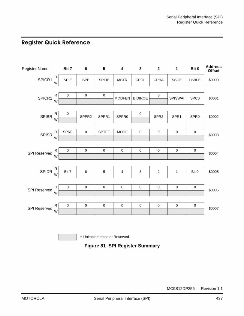
Serial Peripheral Interface (SPI)Register Quick Reference
MC9S12DP256 — Revision 1.1
MOTOROLA Serial Peripheral Interface (SPI) 437
Register Quick Reference
Figure 81 SPI Register Summary
Register Name Bit 7 6 5 4 3 2 1 Bit 0 AddressOffset
SPICR1R
SPIE SPE SPTIE MSTR CPOL CPHA SSOE LSBFE $0000W
SPICR2R 0 0 0
MODFEN BIDIROE0
SPISWAI SPC0 $0001W
SPIBRR 0
SPPR2 SPPR1 SPPR00
SPR2 SPR1 SPR0 $0002W
SPISRR SPRF 0 SPTEF MODF 0 0 0 0
$0003W
SPI ReservedR 0 0 0 0 0 0 0 0
$0004W
SPIDRR
Bit 7 6 5 4 3 2 1 Bit 0 $0005W
SPI ReservedR 0 0 0 0 0 0 0 0
$0006W
SPI ReservedR 0 0 0 0 0 0 0 0
$0007W
= Unimplemented or Reserved

Serial Peripheral Interface (SPI)
MC9S12DP256 — Revision 1.1
438 Serial Peripheral Interface (SPI) MOTOROLA
Register Descriptions
This section consists of register descriptions in address order. Each description includes a standard register diagram with an associated figure number. Details of register bit and field function follow the register diagrams, in bit order.
SPI Control Register 1 (SPICR1)
Read: anytime Write: anytime
SPIE — SPI Interrupt Enable Bit
This bit enables SPI interrupts each time the SPIF or MODF status flag is set.
1 = SPI interrupts enabled.0 = SPI interrupts disabled.
SPE — SPI System Enable Bit
This bit enables the SPI system and dedicates the SPI port pins to SPI system functions. When SPE is clear, the SPI system is initialized but in a low-power disabled state.
1 = SPI port pins are dedicated to SPI functions.0 = SPI system is in a low-power, disabled state.
SPTIE — SPI Transmit Interrupt Enable
This bit enables SPI interrupt generated each time the SPTEF flag is set.
1 = SPTEF interrupt enabled.0 = SPTEF interrupt disabled.
Address Offset: $0000
Bit 7 6 5 4 3 2 1 Bit 0
RSPIE SPE SPTIE MSTR CPOL CPHA SSOE LSBFE
W
Reset: 0 0 0 0 0 1 0 0

Serial Peripheral Interface (SPI)Register Descriptions
MC9S12DP256 — Revision 1.1
MOTOROLA Serial Peripheral Interface (SPI) 439
MSTR — SPI Master/Slave Mode Select Bit1 = Master mode0 = Slave mode
CPOL — SPI Clock Polarity Bit
This bit selects an inverted or non-inverted SPI clock. To transmit data between SPI modules, the SPI modules must have identical CPOL values.
1 = Active-low clocks selected; SCK idles high0 = Active-high clocks selected; SCK idles low
CPHA — SPI Clock Phase Bit
This bit is used to shift the SCK serial clock.1 = The first SCK edge is issued at the beginning of the 8-cycle
transfer operation0 = The first SCK edge is issued one-half cycle into the 8-cycle
transfer operation
SSOE — Slave Select Output Enable
The SS output feature is enabled only in the master mode by asserting the SSOE as shown in Table 76.
LSBFE — SPI LSB-First Enable
This bit does not affect the position of the msb and lsb in the data register. Reads and writes of the data register always have the msb in bit 7.
1 = Data is transferred least significant bit first.0 = Data is transferred most significant bit first.
Table 76 SS Input / Output Selection
MODFEN SSOE Master Mode Slave Mode
0 0 ---- SS input
0 1 ---- SS input
1 0 SS input with MODF feature SS input
1 1 SS output SS input

Serial Peripheral Interface (SPI)
MC9S12DP256 — Revision 1.1
440 Serial Peripheral Interface (SPI) MOTOROLA
SPI Control Register 2 (SPICR2)
Read: anytime Write: anytime; writes to unimplemented bits have no effect
MODFEN — Mode Fault Enable Bit
This bit when set allows the MODF flag to be set. If the MODF flag is set, clearing the MODFEN does not clear the MODF flag. If the SPI is enabled as master and the MODFEN bit is low, then the SS is available as a general purpose I/O.
When the SPI is enabled as a slave, the SS is available only as an input regardless of the value of MODFEN.
1 = Enable setting the MODF error0 = Disable the MODF error
BIDIROE — Output enable in the Bidirectional mode of operation
This bit along with the MSTR bit of SPCR1 is used to enable the output buffer when the SPI is configured in bidirectional mode.
1 = Output buffer enabled0 = Output buffer disabled
SPISWAI — SPI Stop in Wait Mode Bit
This bit is used for power conservation while in wait mode.1 = Stop SPI clock generation when in wait mode0 = SPI clock operates normally in wait mode
SPC0 — Serial Pin Control Bit 0
With the MSTR control bit, this bit enables bidirectional pin configurations as shown in Table 77.
Address Offset: $0001
Bit 7 6 5 4 3 2 1 Bit 0
R 0 0 0MODFEN BIDIROE
0SPISWAI SPC0
W
Reset: 0 0 0 0 0 0 0 0
= Unimplemented or Reserved
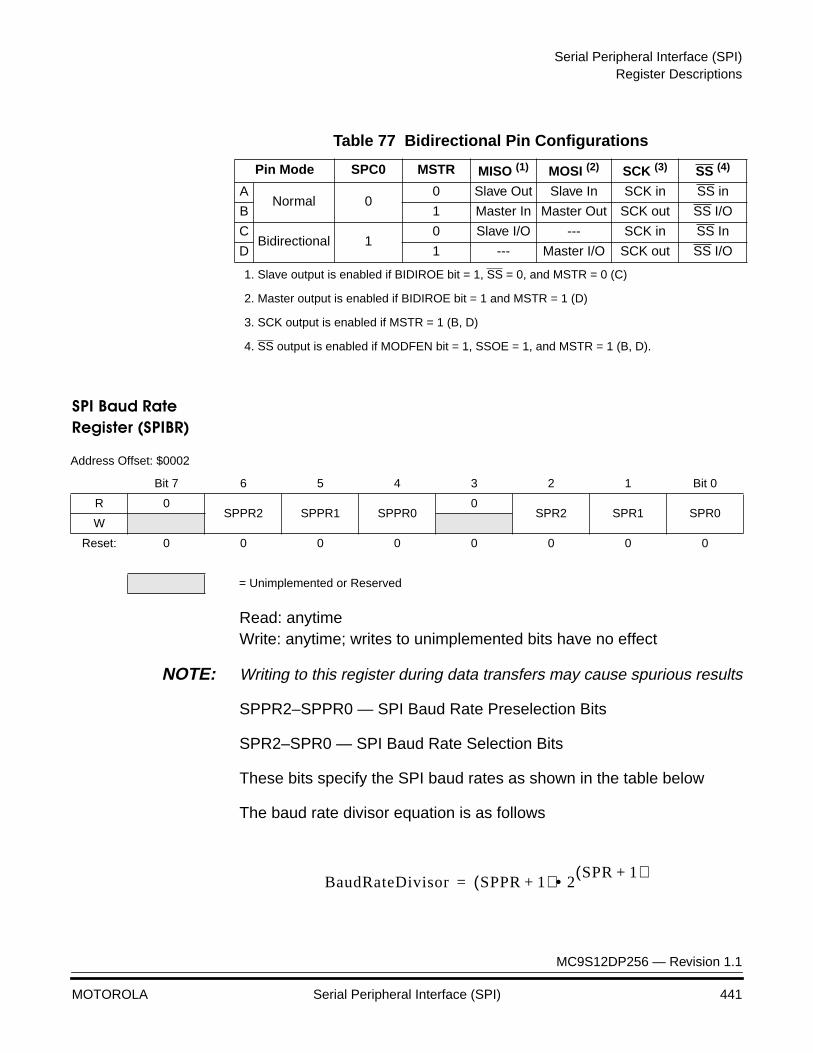
Serial Peripheral Interface (SPI)Register Descriptions
MC9S12DP256 — Revision 1.1
MOTOROLA Serial Peripheral Interface (SPI) 441
SPI Baud Rate Register (SPIBR)
Read: anytime Write: anytime; writes to unimplemented bits have no effect
NOTE: Writing to this register during data transfers may cause spurious results
SPPR2–SPPR0 — SPI Baud Rate Preselection Bits
SPR2–SPR0 — SPI Baud Rate Selection Bits
These bits specify the SPI baud rates as shown in the table below
The baud rate divisor equation is as follows
Table 77 Bidirectional Pin Configurations
Pin Mode SPC0 MSTR MISO (1)
1. Slave output is enabled if BIDIROE bit = 1, SS = 0, and MSTR = 0 (C)
MOSI (2)
2. Master output is enabled if BIDIROE bit = 1 and MSTR = 1 (D)
SCK (3)
3. SCK output is enabled if MSTR = 1 (B, D)
SS (4)
4. SS output is enabled if MODFEN bit = 1, SSOE = 1, and MSTR = 1 (B, D).
ANormal 0
0 Slave Out Slave In SCK in SS in
B 1 Master In Master Out SCK out SS I/O
CBidirectional 1
0 Slave I/O --- SCK in SS In
D 1 --- Master I/O SCK out SS I/O
Address Offset: $0002
Bit 7 6 5 4 3 2 1 Bit 0
R 0SPPR2 SPPR1 SPPR0
0SPR2 SPR1 SPR0
W
Reset: 0 0 0 0 0 0 0 0
= Unimplemented or Reserved
BaudRateDivisor SPPR 1+( ) 2• SPR 1+( )=
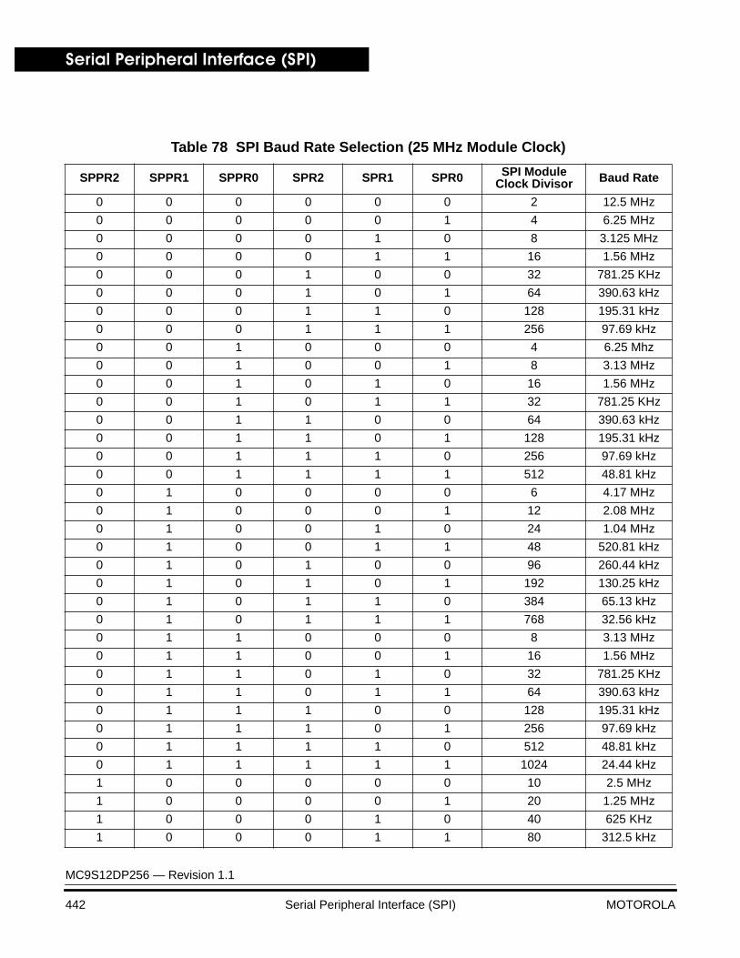
Serial Peripheral Interface (SPI)
MC9S12DP256 — Revision 1.1
442 Serial Peripheral Interface (SPI) MOTOROLA
Table 78 SPI Baud Rate Selection (25 MHz Module Clock)
SPPR2 SPPR1 SPPR0 SPR2 SPR1 SPR0 SPI ModuleClock Divisor Baud Rate
0 0 0 0 0 0 2 12.5 MHz
0 0 0 0 0 1 4 6.25 MHz
0 0 0 0 1 0 8 3.125 MHz
0 0 0 0 1 1 16 1.56 MHz
0 0 0 1 0 0 32 781.25 KHz
0 0 0 1 0 1 64 390.63 kHz
0 0 0 1 1 0 128 195.31 kHz
0 0 0 1 1 1 256 97.69 kHz
0 0 1 0 0 0 4 6.25 Mhz
0 0 1 0 0 1 8 3.13 MHz
0 0 1 0 1 0 16 1.56 MHz
0 0 1 0 1 1 32 781.25 KHz
0 0 1 1 0 0 64 390.63 kHz
0 0 1 1 0 1 128 195.31 kHz
0 0 1 1 1 0 256 97.69 kHz
0 0 1 1 1 1 512 48.81 kHz
0 1 0 0 0 0 6 4.17 MHz
0 1 0 0 0 1 12 2.08 MHz
0 1 0 0 1 0 24 1.04 MHz
0 1 0 0 1 1 48 520.81 kHz
0 1 0 1 0 0 96 260.44 kHz
0 1 0 1 0 1 192 130.25 kHz
0 1 0 1 1 0 384 65.13 kHz
0 1 0 1 1 1 768 32.56 kHz
0 1 1 0 0 0 8 3.13 MHz
0 1 1 0 0 1 16 1.56 MHz
0 1 1 0 1 0 32 781.25 KHz
0 1 1 0 1 1 64 390.63 kHz
0 1 1 1 0 0 128 195.31 kHz
0 1 1 1 0 1 256 97.69 kHz
0 1 1 1 1 0 512 48.81 kHz
0 1 1 1 1 1 1024 24.44 kHz
1 0 0 0 0 0 10 2.5 MHz
1 0 0 0 0 1 20 1.25 MHz
1 0 0 0 1 0 40 625 KHz
1 0 0 0 1 1 80 312.5 kHz
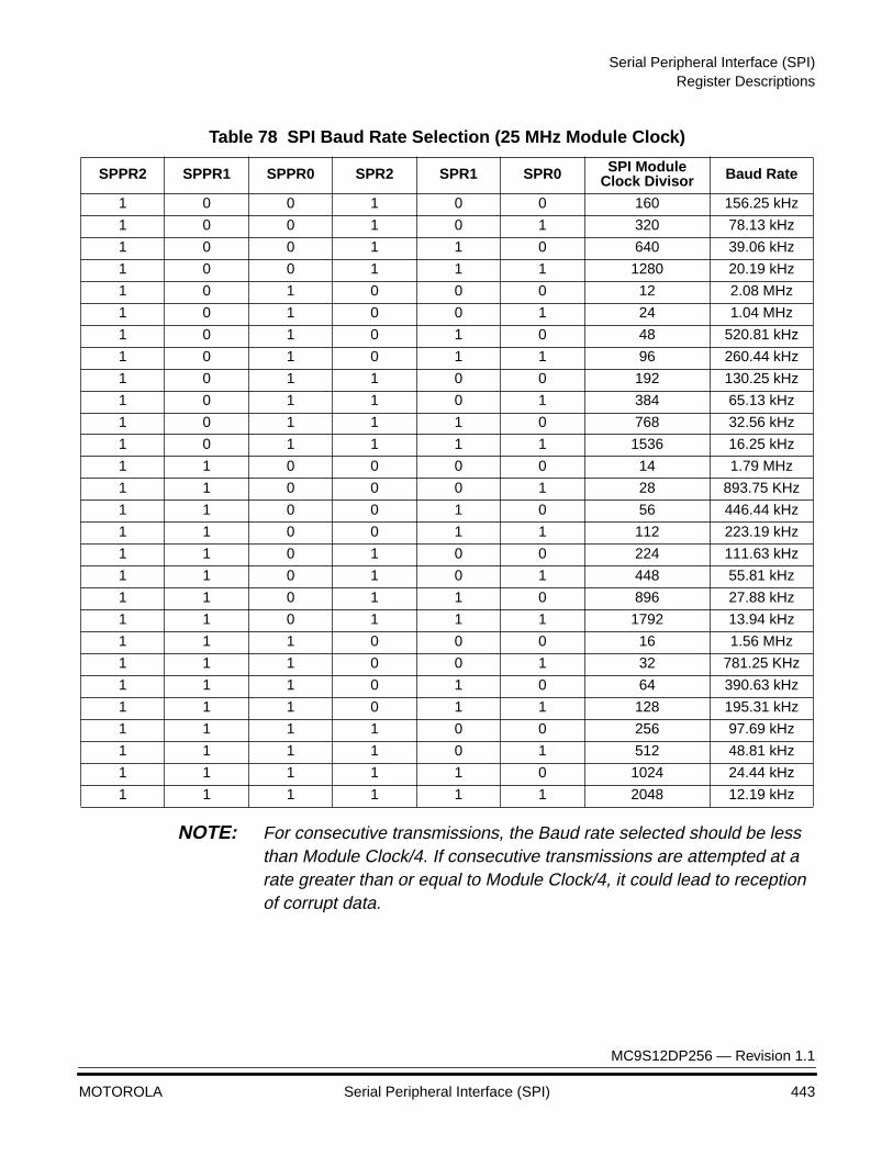
Serial Peripheral Interface (SPI)Register Descriptions
MC9S12DP256 — Revision 1.1
MOTOROLA Serial Peripheral Interface (SPI) 443
NOTE: For consecutive transmissions, the Baud rate selected should be less than Module Clock/4. If consecutive transmissions are attempted at a rate greater than or equal to Module Clock/4, it could lead to reception of corrupt data.
1 0 0 1 0 0 160 156.25 kHz
1 0 0 1 0 1 320 78.13 kHz
1 0 0 1 1 0 640 39.06 kHz
1 0 0 1 1 1 1280 20.19 kHz
1 0 1 0 0 0 12 2.08 MHz
1 0 1 0 0 1 24 1.04 MHz
1 0 1 0 1 0 48 520.81 kHz
1 0 1 0 1 1 96 260.44 kHz
1 0 1 1 0 0 192 130.25 kHz
1 0 1 1 0 1 384 65.13 kHz
1 0 1 1 1 0 768 32.56 kHz
1 0 1 1 1 1 1536 16.25 kHz
1 1 0 0 0 0 14 1.79 MHz
1 1 0 0 0 1 28 893.75 KHz
1 1 0 0 1 0 56 446.44 kHz
1 1 0 0 1 1 112 223.19 kHz
1 1 0 1 0 0 224 111.63 kHz
1 1 0 1 0 1 448 55.81 kHz
1 1 0 1 1 0 896 27.88 kHz
1 1 0 1 1 1 1792 13.94 kHz
1 1 1 0 0 0 16 1.56 MHz
1 1 1 0 0 1 32 781.25 KHz
1 1 1 0 1 0 64 390.63 kHz
1 1 1 0 1 1 128 195.31 kHz
1 1 1 1 0 0 256 97.69 kHz
1 1 1 1 0 1 512 48.81 kHz
1 1 1 1 1 0 1024 24.44 kHz
1 1 1 1 1 1 2048 12.19 kHz
Table 78 SPI Baud Rate Selection (25 MHz Module Clock)
SPPR2 SPPR1 SPPR0 SPR2 SPR1 SPR0 SPI ModuleClock Divisor Baud Rate

Serial Peripheral Interface (SPI)
MC9S12DP256 — Revision 1.1
444 Serial Peripheral Interface (SPI) MOTOROLA
SPI Status Register (SPISR)
Read: anytimeWrite: has no meaning or effect
SPRF — SPRF Receive Interrupt Flag
This bit is set after the eighth SCK cycle in a data transfer and is cleared by reading the SPISR register (with SPIF set) followed by a read access to the SPI data register.
1 = New data Copied to SPIDR0 = Transfer not yet complete
SPTEF — SPI Transmit Empty Interrupt Flag
This bit is set each time the transmit data register transfers a byte into the shift register. SPTEF generates an SPTEF CPU interrupt request if the SPTIE bit in the SPICR1 is also set.This bit is cleared by reading the SPISR register (with SPTEF set) followed by a write access to the SPI data register.For an idle master or idle slave that has no data loaded into its transmit buffer, the SPTEF will be set again within two bus cycles since the transmit buffer empties into the shift register. This allows the user to queue up 16-bit value to send. For an already active slave, the load of the shift register cannot occur until the transmission is complete.The SPTEF indicates when the next write can occur
1 = SPI Data register empty0 = SPI Data register not empty
Address Offset: $0003
Bit 7 6 5 4 3 2 1 Bit 0
R SPRF 0 SPTEF MODF 0 0 0 0
W
Reset: 0 0 1 0 0 0 0 0
= Unimplemented or Reserved

Serial Peripheral Interface (SPI)Register Descriptions
MC9S12DP256 — Revision 1.1
MOTOROLA Serial Peripheral Interface (SPI) 445
MODF — Mode Fault Flag
This bit is set if the SS input becomes low while the SPI is configured as a master. The flag is cleared automatically by a read of the SPI status register (with MODF set) followed by a write to the SPI control register 1. The MODF flag is set only if the MODFEN bit of SPICR2 register is set, Refer to MODFEN bit description in SPI Control Register 2 (SPICR2).
1 = Mode fault has occurred.0 = Mode fault has not occurred.
SPI Data Register (SPIDR)
Read: anytime; normally read only after SPIF is set Write: anytime; see SPTEF
The SPI Data register is both the input and output register for SPI data. A write to this register allows a data byte to be queued and transmitted. For a SPI configured as a master, a queued data byte is transmitted immediately after the previous transmission has completed. The SPI Transmitter empty flag in SPISR indicates when the SPI data register is ready to accept new data.
NOTE: Do not write to the SPI data register unless the SPTEF bit is high.
Reading the data can occur anytime from after the SPIF is set to before the end of the next transfer. If the SPIF is not serviced by the end of the successive transfers, those data bytes are lost and the data within the SPIDR retains the first byte until SPIF is serviced.
Address Offset: $0005
Bit 7 6 5 4 3 2 1 Bit 0
RBit 7 6 5 4 3 2 2 Bit 0
W
Reset: 0 0 0 0 0 0 0 0
Serial Peripheral Interface (SPI)
MC9S12DP256 — Revision 1.1
446 Serial Peripheral Interface (SPI) MOTOROLA
Functional Description
The SPI module allows full-duplex, synchronous, serial communication between the MCU and peripheral devices. Software can poll the SPI status flags or SPI operation can be interrupt driven.
The SPI system is enabled by setting the SPI enable (SPE) bit in SPI control register 1. While SPE is set, the four associated SPI port pins are dedicated to the SPI function as:
• Slave select (SS)
• Serial clock (SCK)
• Master out/slave in (MOSI)
• Master in/slave out (MISO)
The main element of the SPI system is the SPI data register. The 8-bit data register in the master and the 8-bit data register in the slave are linked by the MOSI and MISO pins to form a distributed 16-bit register. When a data transfer operation is performed, this 16-bit register is serially shifted eight bit positions by the SCK clock from the master; data is exchanged between the master and the slave. Data written to the master SPI data register becomes the output data for the slave, and data read from the master SPI data register after a transfer operation is the input data from the slave.
A write to the SPI data register puts data into the transmit buffer if the previous transmission was complete. When a transfer is complete, received data is moved into a receive data register. Data may be read from this double-buffered system any time before the next transfer is complete. This 8-bit data register acts as the SPI receive data register for reads and as the SPI transmit data register for writes. A single SPI register address is used for reading data from the read data buffer and for writing data to the shifter.
The clock phase control bit (CPHA) and a clock polarity control bit (CPOL) in the SPI control register 1 select one of four possible clock formats to be used by the SPI system. The CPOL bit simply selects a non-inverted or inverted clock. The CPHA bit is used to accommodate
Serial Peripheral Interface (SPI)Functional Description
MC9S12DP256 — Revision 1.1
MOTOROLA Serial Peripheral Interface (SPI) 447
two fundamentally different protocols by shifting the clock by a half cycle or by not shifting the clock (see Transmission Formats).
The SPI can be configured to operate as a master or as a slave. When MSTR in SPI control register1 is set, the master mode is selected; when the MSTR bit is clear, the slave mode is selected.
Master Mode The SPI operates in master mode when the MSTR bit is set. Only a master SPI module can initiate transmissions. A transmission begins by writing to the master SPI data register. If the shift register is empty, the byte immediately transfers to the shift register. The byte begins shifting out on the MOSI pin under the control of the serial clock.
The SPR2, SPR1, and SPR0 baud rate selection bits in conjunction with the SPPR2, SPPR1, and SPPR0 baud rate preselection bits in the SPI baud rate register control the baud rate generator and determine the speed of the shift register. The SCK pin is the SPI clock output. Through the SCK pin, the baud rate generator of the master controls the shift register of the slave peripheral.
Consecutive transmissions are possible but care should be taken to set the Baud rate selection bits to correspond to a frequency less than busclock/4.
In master mode, the function of the serial data output pin (MOSI) and the serial data input pin (MISO) is determined by the SPC0 and MSTR control bits.
The SS pin is normally an input which should remain in the inactive high state. However, in the master mode, if both MODFEN bit and SSOE bit are set, then the SS pin is the slave select output.
The SS output becomes low during each transmission and is high when the SPI is in the idling state. If the SS input becomes low while the SPI is configured as a master, it indicates a mode fault error where more than one master may be trying to drive the MOSI and SCK lines simultaneously. In this case, the SPI immediately clears the output buffer enables associated with the MISO, MOSI (or MOMI), and SCK pins so that these pins become inputs. This mode fault error also clears the SPE and MSTR control bits and sets the mode fault (MODF) flag in the SPI
Serial Peripheral Interface (SPI)
MC9S12DP256 — Revision 1.1
448 Serial Peripheral Interface (SPI) MOTOROLA
status register. If the SPI interrupt enable bit (SPIE) is set when the MODF bit gets set, then an SPI interrupt sequence is also requested
When a write to the SPI data register in the master occurs, there is a half SCK-cycle delay. After the delay, SCK is started within the master. The rest of the transfer operation differs slightly, depending on the clock format specified by the SPI clock phase bit, CPHA, in SPI control register 1 (see Transmission Formats).
Slave Mode The SPI operates in slave mode when the MSTR bit in SPI control register1 is clear. In slave mode, SCK is the SPI clock input from the master, and SS is the slave select input. Before a data transmission occurs, the SS pin of the slave SPI must be at logic 0. SS must remain low until the transmission is complete.
In slave mode, the function of the serial data output pin (MISO) and serial data input pin (MOSI) is determined by the SPC0 bit in SPI control register 2 and the MSTR control bit. While in slave mode, the SS input controls the serial data output pin; if SS is high (not selected), the serial data output pin is high impedance, and, if SS is low the first bit in the SPI data register is driven out of the serial data output pin. Also, if the slave is not selected (SS is high), then the SCK input is ignored and no internal shifting of the SPI shift register takes place.
Although the SPI is capable of full-duplex operation, some SPI peripherals are capable of only receiving SPI data in a slave mode. For these simpler devices, there is no serial data out pin.
NOTE: When peripherals with full-duplex capability are used, take care not to simultaneously enable two receivers whose serial outputs drive the same system slave’s serial data output line.
As long as no more than one slave device drives the system slave’s serial data output line, it is possible for several slaves to receive the same transmission from a master, although the master would not receive return information from all of the receiving slaves.
If the CPHA bit in SPI control register 1 is clear, odd numbered edges on the SCK input cause the data at the serial data input pin to be latched.
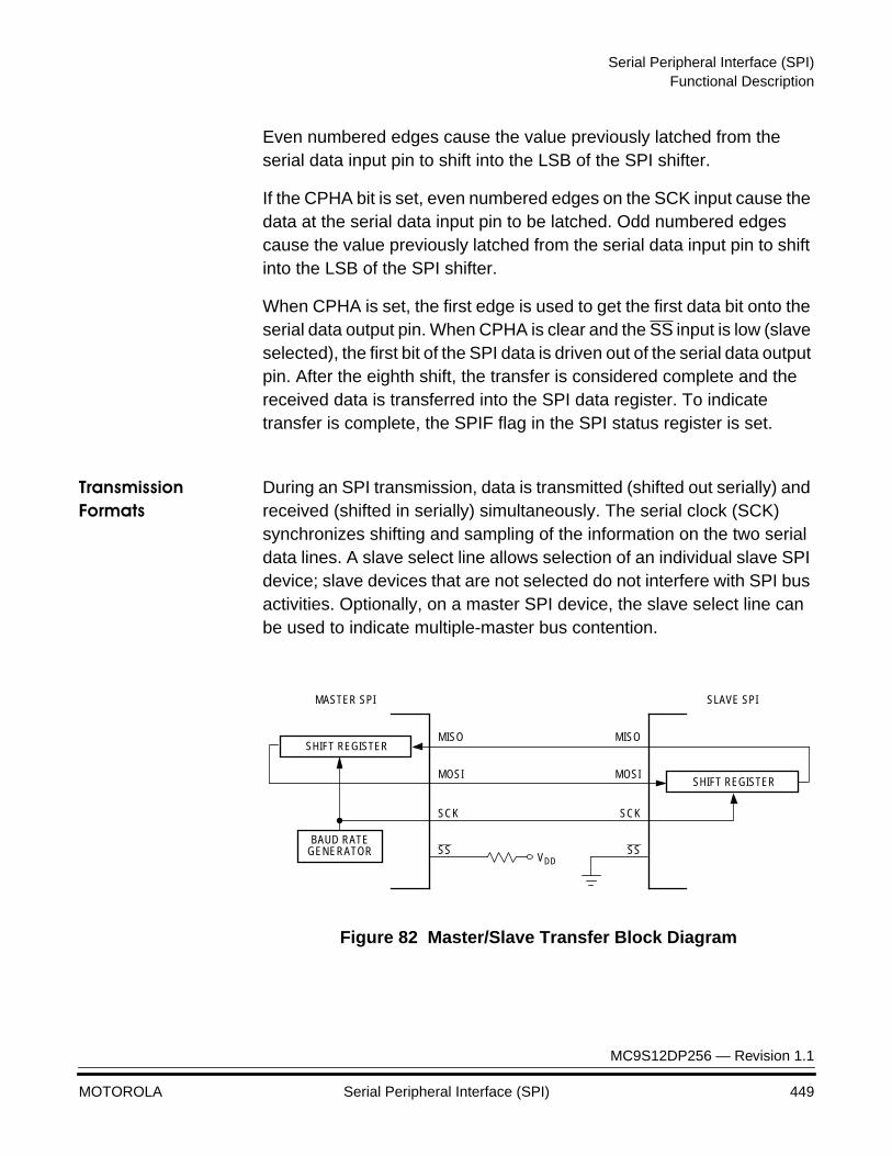
Serial Peripheral Interface (SPI)Functional Description
MC9S12DP256 — Revision 1.1
MOTOROLA Serial Peripheral Interface (SPI) 449
Even numbered edges cause the value previously latched from the serial data input pin to shift into the LSB of the SPI shifter.
If the CPHA bit is set, even numbered edges on the SCK input cause the data at the serial data input pin to be latched. Odd numbered edges cause the value previously latched from the serial data input pin to shift into the LSB of the SPI shifter.
When CPHA is set, the first edge is used to get the first data bit onto the serial data output pin. When CPHA is clear and the SS input is low (slave selected), the first bit of the SPI data is driven out of the serial data output pin. After the eighth shift, the transfer is considered complete and the received data is transferred into the SPI data register. To indicate transfer is complete, the SPIF flag in the SPI status register is set.
Transmission Formats
During an SPI transmission, data is transmitted (shifted out serially) and received (shifted in serially) simultaneously. The serial clock (SCK) synchronizes shifting and sampling of the information on the two serial data lines. A slave select line allows selection of an individual slave SPI device; slave devices that are not selected do not interfere with SPI bus activities. Optionally, on a master SPI device, the slave select line can be used to indicate multiple-master bus contention.
Figure 82 Master/Slave Transfer Block Diagram
SHIFT REGISTER
SHIFT REGISTER
BAUD RATEGENERATOR
MASTER SPI SLAVE SPI
VDD
MOSI MOSI
MISO MISO
SCK SCK
SS SS
Serial Peripheral Interface (SPI)
MC9S12DP256 — Revision 1.1
450 Serial Peripheral Interface (SPI) MOTOROLA
Clock Phase and Polarity Controls
Using two bits in the SPI control register1, software selects one of four combinations of serial clock phase and polarity.
The CPOL clock polarity control bit specifies an active high or low clock and has no significant effect on the transmission format.
The CPHA clock phase control bit selects one of two fundamentally different transmission formats.
Clock phase and polarity should be identical for the master SPI device and the communicating slave device. In some cases, the phase and polarity are changed between transmissions to allow a master device to communicate with peripheral slaves having different requirements.
CPHA = 0 Transfer Format
The first edge on the SCK line is used to clock the first data bit of slave into the master and the first data bit of master into the slave. In some peripherals, the first bit of the slave's data is available at the slave data out pin as soon as the slave is selected. In this format, the first SCK edge is not issued until a half cycle into the 8-cycle transfer operation. The first edge of SCK is delayed a half cycle by clearing the CPHA bit.
The SCK output from the master remains in the inactive state for a half SCK period before the first edge appears. A half SCK cycle later, the second edge appears on the SCK line. When this second edge occurs, the value previously latched from the serial data input pin is shifted into the LSB of the shifter.
After this second edge, the next bit of the SPI master data is transmitted out of the serial data output pin of the master to the serial input pin on the slave. This process continues for a total of 16 edges on the SCK line, with data being latched on odd numbered edges and shifted on even numbered edges.
Data reception is double buffered. Data is shifted serially into the SPI shift register during the transfer and is transferred to the parallel SPI data register after the last bit is shifted in.
After the 16th (last) SCK edge:
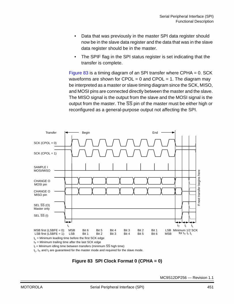
Serial Peripheral Interface (SPI)Functional Description
MC9S12DP256 — Revision 1.1
MOTOROLA Serial Peripheral Interface (SPI) 451
• Data that was previously in the master SPI data register should now be in the slave data register and the data that was in the slave data register should be in the master.
• The SPIF flag in the SPI status register is set indicating that the transfer is complete.
Figure 83 is a timing diagram of an SPI transfer where CPHA = 0. SCK waveforms are shown for CPOL = 0 and CPOL = 1. The diagram may be interpreted as a master or slave timing diagram since the SCK, MISO, and MOSI pins are connected directly between the master and the slave. The MISO signal is the output from the slave and the MOSI signal is the output from the master. The SS pin of the master must be either high or reconfigured as a general-purpose output not affecting the SPI.
Figure 83 SPI Clock Format 0 (CPHA = 0)
tL
Begin End
SCK (CPOL = 0)
SAMPLE I
CHANGE O
SEL SS (O)
Transfer
SCK (CPOL = 1)
MSB first (LSBFE = 0): LSB first (LSBFE = 1):
MSBLSB
LSBMSB
Bit 5Bit 2
Bit 6Bit 1
Bit 4Bit 3
Bit 3Bit 4
Bit 2Bit 5
Bit 1Bit 6
CHANGE O
SEL SS (I)
MOSI pin
MISO pin
Master only
MOSI/MISO
tT
If ne
xt tr
ansf
er b
egin
s he
re
for tT, tl, tLMinimum 1/2 SCK
tI tL
tL = Minimum leading time before the first SCK edgetT = Minimum trailing time after the last SCK edgetI = Minimum idling time between transfers (minimum SS high time)tL, tT, and tI are guaranteed for the master mode and required for the slave mode.
Serial Peripheral Interface (SPI)
MC9S12DP256 — Revision 1.1
452 Serial Peripheral Interface (SPI) MOTOROLA
The SS line can remain active low between successive transfers.
NOTE: There is a functional hazard, the SPI may lose data in this mode (CPHA=0) if configured as a slave with the SCK rate at div2 of the slave’s module clock (see Errata).
CPHA = 1 Transfer Format
Some peripherals require the first SCK edge before the first data bit becomes available at the data out pin; the second edge clocks data into the system. In this format, the first SCK edge is issued by setting the CPHA bit at the beginning of the 8-cycle transfer operation.
The first edge of SCK occurs immediately after the half SCK clock cycle synchronization delay. This first edge commands the slave to transfer its most significant data bit to the serial data input pin of the master.
A half SCK cycle later, the second edge appears on the SCK pin. This is the latching edge for both the master and slave.
When the third edge occurs, the value previously latched from the serial data input pin is shifted into the LSB of the SPI shifter. After this edge, the next bit of the master data is coupled out of the serial data output pin of the master to the serial input pins on the slave.
This process continues for a total of 16 edges on the SCK line with data being latched on even numbered edges and shifting taking place on odd numbered edges.
Data reception is double buffered; data is serially shifted into the SPI shift register during the transfer and is transferred to the parallel SPI data register after the last bit is shifted in.
After the 16th SCK edge:
• Data that was previously in the SPI data register of the master is now in the data register of the slave, and data that was in the data register of the slave is in the master.
• The SPIF flag bit in SPISR is set indicating that the transfer is complete.
Figure 84 shows two clocking variations for CPHA = 1. The diagram may be interpreted as a master or slave timing diagram since the SCK, MISO,
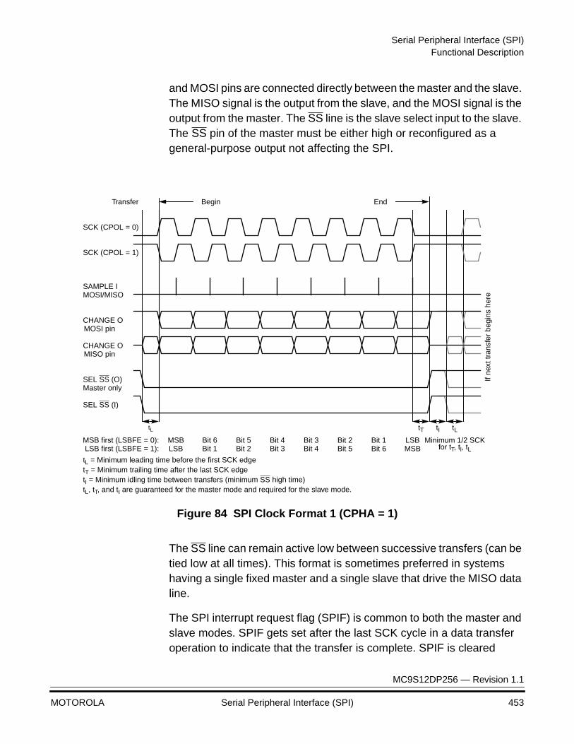
Serial Peripheral Interface (SPI)Functional Description
MC9S12DP256 — Revision 1.1
MOTOROLA Serial Peripheral Interface (SPI) 453
and MOSI pins are connected directly between the master and the slave. The MISO signal is the output from the slave, and the MOSI signal is the output from the master. The SS line is the slave select input to the slave. The SS pin of the master must be either high or reconfigured as a general-purpose output not affecting the SPI.
Figure 84 SPI Clock Format 1 (CPHA = 1)
The SS line can remain active low between successive transfers (can be tied low at all times). This format is sometimes preferred in systems having a single fixed master and a single slave that drive the MISO data line.
The SPI interrupt request flag (SPIF) is common to both the master and slave modes. SPIF gets set after the last SCK cycle in a data transfer operation to indicate that the transfer is complete. SPIF is cleared
tL tT
for tT, tl, tLMinimum 1/2 SCK
tI tL
If ne
xt tr
ansf
er b
egin
s he
re
Begin End
SCK (CPOL = 0)
SAMPLE I
CHANGE O
SEL SS (O)
Transfer
SCK (CPOL = 1)
MSB first (LSBFE = 0): LSB first (LSBFE = 1):
MSBLSB
LSBMSB
Bit 5Bit 2
Bit 6Bit 1
Bit 4Bit 3
Bit 3Bit 4
Bit 2Bit 5
Bit 1Bit 6
CHANGE O
SEL SS (I)
MOSI pin
MISO pin
Master only
MOSI/MISO
tL = Minimum leading time before the first SCK edgetT = Minimum trailing time after the last SCK edgetI = Minimum idling time between transfers (minimum SS high time)tL, tT, and tI are guaranteed for the master mode and required for the slave mode.
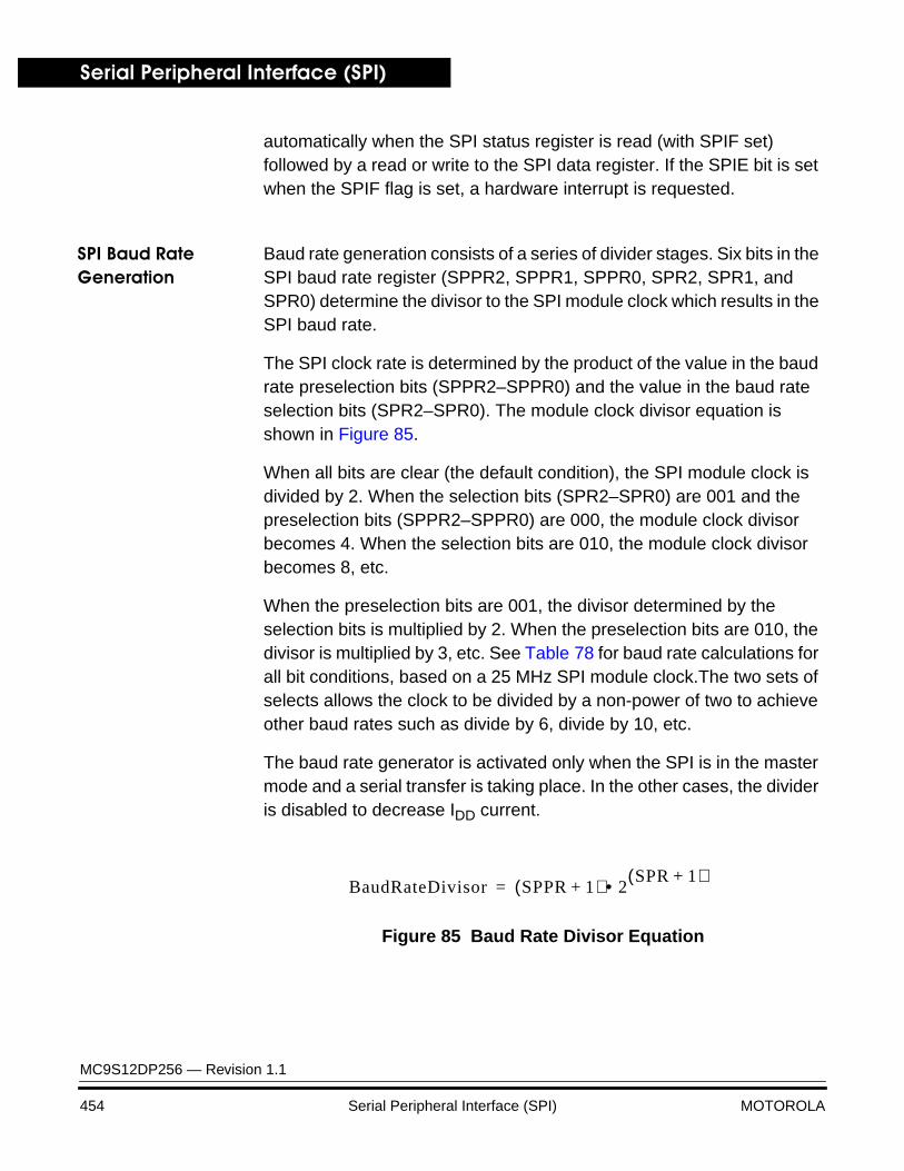
Serial Peripheral Interface (SPI)
MC9S12DP256 — Revision 1.1
454 Serial Peripheral Interface (SPI) MOTOROLA
automatically when the SPI status register is read (with SPIF set) followed by a read or write to the SPI data register. If the SPIE bit is set when the SPIF flag is set, a hardware interrupt is requested.
SPI Baud Rate Generation
Baud rate generation consists of a series of divider stages. Six bits in the SPI baud rate register (SPPR2, SPPR1, SPPR0, SPR2, SPR1, and SPR0) determine the divisor to the SPI module clock which results in the SPI baud rate.
The SPI clock rate is determined by the product of the value in the baud rate preselection bits (SPPR2–SPPR0) and the value in the baud rate selection bits (SPR2–SPR0). The module clock divisor equation is shown in Figure 85.
When all bits are clear (the default condition), the SPI module clock is divided by 2. When the selection bits (SPR2–SPR0) are 001 and the preselection bits (SPPR2–SPPR0) are 000, the module clock divisor becomes 4. When the selection bits are 010, the module clock divisor becomes 8, etc.
When the preselection bits are 001, the divisor determined by the selection bits is multiplied by 2. When the preselection bits are 010, the divisor is multiplied by 3, etc. See Table 78 for baud rate calculations for all bit conditions, based on a 25 MHz SPI module clock.The two sets of selects allows the clock to be divided by a non-power of two to achieve other baud rates such as divide by 6, divide by 10, etc.
The baud rate generator is activated only when the SPI is in the master mode and a serial transfer is taking place. In the other cases, the divider is disabled to decrease IDD current.
Figure 85 Baud Rate Divisor Equation
BaudRateDivisor SPPR 1+( ) 2• SPR 1+( )=

Serial Peripheral Interface (SPI)Functional Description
MC9S12DP256 — Revision 1.1
MOTOROLA Serial Peripheral Interface (SPI) 455
Special Features
SS Output The SS output feature automatically drives the SS pin low during transmission to select external devices and drives it high during idle to deselect external devices. When SS output is selected, the SS output pin is connected to the SS input pin of the external device.
The SS output is available only in master mode during normal SPI operation by asserting SSOE and MODFEN bit as shown in Table 76.
The mode fault feature is disabled while SS output is enabled.
NOTE: Care must be taken when using the SS output feature in a multimaster system since the mode fault feature is not available for detecting system errors between masters.
Bidirectional Mode (MOMI or SISO)
The bidirectional mode is selected when the SPC0 bit is set in SPI control register 2 (see Normal Mode and Bidirectional Mode). In this mode, the SPI uses only one serial data pin for the interface with external device(s). The MSTR bit decides which pin to use. The MOSI pin becomes the serial data I/O (MOMI) pin for the master mode, and the MISO pin becomes serial data I/O (SISO) pin for the slave mode. The MISO pin in the master mode and MOSI pin in the slave mode become general-purpose I/O.
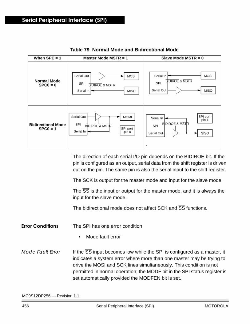
Serial Peripheral Interface (SPI)
MC9S12DP256 — Revision 1.1
456 Serial Peripheral Interface (SPI) MOTOROLA
The direction of each serial I/O pin depends on the BIDIROE bit. If the pin is configured as an output, serial data from the shift register is driven out on the pin. The same pin is also the serial input to the shift register.
The SCK is output for the master mode and input for the slave mode.
The SS is the input or output for the master mode, and it is always the input for the slave mode.
The bidirectional mode does not affect SCK and SS functions.
Error Conditions The SPI has one error condition
• Mode fault error
Mode Fault Error If the SS input becomes low while the SPI is configured as a master, it indicates a system error where more than one master may be trying to drive the MOSI and SCK lines simultaneously. This condition is not permitted in normal operation; the MODF bit in the SPI status register is set automatically provided the MODFEN bit is set.
Table 79 Normal Mode and Bidirectional Mode
When SPE = 1 Master Mode MSTR = 1 Slave Mode MSTR = 0
Normal ModeSPC0 = 0
Bidirectional ModeSPC0 = 1
SPI
MOSI
MISO
BIDIROE & MSTR
Serial Out
Serial In
SPI
MOSI
MISO
Serial In
Serial Out
BIDIROE & MSTR
SPI
MOMI
SPI port BIDIROE & MSTR
Serial Out
Serial In pin 0
SPI
SISO
BIDIROE & MSTR
Serial In
Serial Out
SPI port pin 1
.
Serial Peripheral Interface (SPI)Low Power Mode Options
MC9S12DP256 — Revision 1.1
MOTOROLA Serial Peripheral Interface (SPI) 457
In the special case where the MODFEN bit is cleared, the SS pin is a general purpose input/output pin for the SPI system configured in master mode. In this special case, the mode error function is inhibited and MODF remains cleared.
In case the SPI system is configured as a slave and the MODFEN bit is cleared the SS pin is a dedicated input pin.
When a mode fault error occurs, the SPE and MSTR bits are cleared thereby clearing the output enable for the SCK, MISO, and MOSI (for MOMI) pins cleared. This forces those pins to be high impedance inputs to avoid any possibility of conflict with another output driver.
If the mode fault error occurs in the bidirectional mode for a SPI system configured in master mode, MISO (SISO) is not affected. No mode fault error occurs in the bidirectional mode for SPI system configured in slave mode.
The mode fault flag is cleared automatically by a read of the SPI status register (with MODF set) followed by a write to SPI control register 1.
Low Power Mode Options
SPI in Run Mode In run mode with the SPI system enable (SPE) bit in the SPI control register clear, the SPI system is in a low-power, disabled state. SPI registers can still be accessed, but clocks to the core of this module are disabled.
SPI in Wait Mode SPI operation in wait mode depends upon the state of the SPISWAI bit in SPI control register 2.
• If SPISWAI is clear, the SPI operates normally when the CPU is in wait mode
• If SPISWAI is set, SPI clock generation ceases and the SPI module enters a power conservation state when the CPU is in wait mode.

Serial Peripheral Interface (SPI)
MC9S12DP256 — Revision 1.1
458 Serial Peripheral Interface (SPI) MOTOROLA
– If SPISWAI is set and the SPI is configured for master, any transmission and reception in progress stops at wait mode entry. The transmission and reception resumes when the SPI exits wait mode.
– If SPISWAI is set and the SPI is configured as a slave, any transmission and reception in progress continues if the SCK continues to be driven from the master. This keeps the slave synchronized to the master and the SCK.
If the master transmits several bytes while the slave is in wait mode, the slave will continue to send out bytes consistent with the its operation mode at the start of wait mode (i.e. If the slave is currently sending its SPIDR to the master, it will continue to send the same byte. Else if the slave is currently sending the last received byte from the master, it will continue to send each previous master byte).
NOTE: Care must be taken when expecting data from a master while the slave is in wait or stop mode. Even though the shift register will continue to operate, the rest of the SPI is shut down (i.e. a SPIF interrupt will not be generated until exiting stop or wait mode). Also, the byte from the shift register will not be copied into the SPIDR register until after the slave SPI has exited wait or stop mode. A SPIF flag and SPIDR copy is only generated if wait mode is entered or exited during a tranmission. If the slave enters wait mode in idle mode and exits wait mode in idle mode, neither a SPIF nor a SPIDR copy will occur.
SPI in Stop Mode Stop mode is dependent on the system. The SPI enters stop mode when the module clock is disabled (held high or low). If the SPI is in master mode and exchanging data when the CPU enters stop mode, the transmission is frozen until the CPU exits stop mode. After stop, data to and from the external SPI is exchanged correctly. In slave mode, the SPI will stay synchronized with the master.
The stop mode is equivalent to the wait mode with the SPISWAI bit set except that the stop mode is not dependent on the SPISWAI bit.
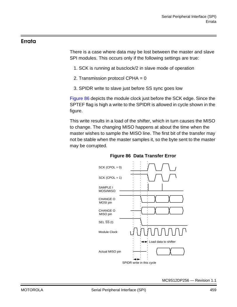
Serial Peripheral Interface (SPI)Errata
MC9S12DP256 — Revision 1.1
MOTOROLA Serial Peripheral Interface (SPI) 459
Errata
There is a case where data may be lost between the master and slave SPI modules. This occurs only if the following settings are true:
1. SCK is running at busclock/2 in slave mode of operation
2. Transmission protocol CPHA = 0
3. SPIDR write to slave just before SS sync goes low
Figure 86 depicts the module clock just before the SCK edge. Since the SPTEF flag is high a write to the SPIDR is allowed in cycle shown in the figure.
This write results in a load of the shifter, which in turn causes the MISO to change. The changing MISO happens at about the time when the master wishes to sample the MISO line. The first bit of the transfer may not be stable when the master samples it, so the byte sent to the master may be corrupted.
Figure 86 Data Transfer Error
SCK (CPOL = 0)
SAMPLE I
CHANGE O
SCK (CPOL = 1)
CHANGE O
SEL SS (I)
MOSI pin
MISO pin
MOSI/MISO
Module Clock
Actual MISO pin
Load data to shifter
SPIDR write in this cycle
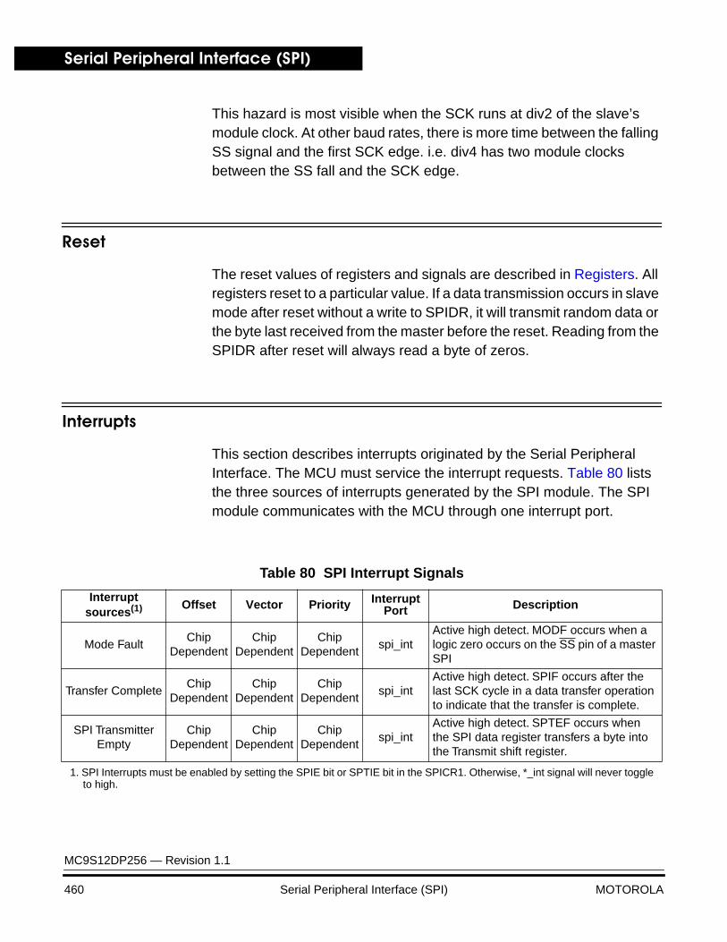
Serial Peripheral Interface (SPI)
MC9S12DP256 — Revision 1.1
460 Serial Peripheral Interface (SPI) MOTOROLA
This hazard is most visible when the SCK runs at div2 of the slave’s module clock. At other baud rates, there is more time between the falling SS signal and the first SCK edge. i.e. div4 has two module clocks between the SS fall and the SCK edge.
Reset
The reset values of registers and signals are described in Registers. All registers reset to a particular value. If a data transmission occurs in slave mode after reset without a write to SPIDR, it will transmit random data or the byte last received from the master before the reset. Reading from the SPIDR after reset will always read a byte of zeros.
Interrupts
This section describes interrupts originated by the Serial Peripheral Interface. The MCU must service the interrupt requests. Table 80 lists the three sources of interrupts generated by the SPI module. The SPI module communicates with the MCU through one interrupt port.
Table 80 SPI Interrupt Signals
Interrupt sources(1) Offset Vector Priority Interrupt
Port Description
Mode FaultChip
DependentChip
DependentChip
Dependentspi_int
Active high detect. MODF occurs when a logic zero occurs on the SS pin of a master SPI
Transfer CompleteChip
DependentChip
DependentChip
Dependentspi_int
Active high detect. SPIF occurs after the last SCK cycle in a data transfer operation to indicate that the transfer is complete.
SPI Transmitter Empty
ChipDependent
ChipDependent
ChipDependent
spi_intActive high detect. SPTEF occurs when the SPI data register transfers a byte into the Transmit shift register.
1. SPI Interrupts must be enabled by setting the SPIE bit or SPTIE bit in the SPICR1. Otherwise, *_int signal will never toggleto high.
Serial Peripheral Interface (SPI)Interrupts
MC9S12DP256 — Revision 1.1
MOTOROLA Serial Peripheral Interface (SPI) 461
Description of Interrupt Operation
The Serial Peripheral Interface only originates interrupt requests. The following is a description of how the Serial Peripheral Interface makes a request and how the MCU should acknowledge that request. The interrupt vector offset and interrupt priority are chip dependent.
MODF Description MODF occurs when the master detects an error on the SS pin. The master SPI must be configured for the MODF feature (see Table 76). Once MODF is set, the current transfer is halted and the following bits are changed:
• SPE=0, The SPI automatically disables itself.
• MSTR=0, The master bit in SPICR1 resets.
The MODF interrupt is reflected in the status register MODF flag. Clearing the flag will also clear the interrupt. This interrupt will stay active while the MODF flag is set. MODF has an automatic clearing process which is described in SPI Status Register (SPISR).
SPIF Description SPIF occurs when the SPI receives/transmits the last SCK edge in a data transfer operation. Once SPIF is set, it does not clear until it is serviced. SPIF has an automatic clearing process which is described in SPI Status Register (SPISR). In the event that the SPIF is not serviced before the end of the next transfer (i.e. SPIF remains active throughout another transfer), the latter transfers will be ignored and no new data will be copied into the SPIDR.
SPTEF Description SPTEF occurs when the SPI Data register transfers a byte into the transmit buffer Once SPTEF is set, it does not clear until it is serviced. SPTEF has an automatic clearing process which is described in SPI Status Register (SPISR).

Serial Peripheral Interface (SPI)
MC9S12DP256 — Revision 1.1
462 Serial Peripheral Interface (SPI) MOTOROLA
MC9S12DP256 — Revision 1.1
MOTOROLA Inter-IC Bus (IIC) 463
Inter-IC Bus (IIC)Inter-IC Bus (IIC)
Contents
Overview . . . . . . . . . . . . . . . . . . . . . . . . . . . . . . . . . . . . . . . . . . . . . . 463Features . . . . . . . . . . . . . . . . . . . . . . . . . . . . . . . . . . . . . . . . . . . . . . 464Modes of Operation. . . . . . . . . . . . . . . . . . . . . . . . . . . . . . . . . . . . . . 464Block Diagram. . . . . . . . . . . . . . . . . . . . . . . . . . . . . . . . . . . . . . . . . . 465Signal Descriptions . . . . . . . . . . . . . . . . . . . . . . . . . . . . . . . . . . . . . . 467Module Memory Map . . . . . . . . . . . . . . . . . . . . . . . . . . . . . . . . . . . . 468Register Quick Reference . . . . . . . . . . . . . . . . . . . . . . . . . . . . . . . . . 469Register Descriptions . . . . . . . . . . . . . . . . . . . . . . . . . . . . . . . . . . . . 469I-Bus Protocol . . . . . . . . . . . . . . . . . . . . . . . . . . . . . . . . . . . . . . . . . . 478Interrupt Operation . . . . . . . . . . . . . . . . . . . . . . . . . . . . . . . . . . . . . . 483Modes of Operation. . . . . . . . . . . . . . . . . . . . . . . . . . . . . . . . . . . . . . 484Programming. . . . . . . . . . . . . . . . . . . . . . . . . . . . . . . . . . . . . . . . . . . 485
Overview
The Inter-IC Bus (IIC or I2C) is a two-wire, bidirectional serial bus that provides a simple, efficient method of data exchange between devices. Being a two-wire device, the IIC Bus minimizes the need for large numbers of connections between devices, and eliminates the need for an address decoder.
This bus is suitable for applications requiring occasional communications over a short distance between a number of devices. It also provides flexibility, allowing additional devices to be connected to the bus for further expansion and system development.
The interface is designed to operate up to 100Kbps with maximum bus loading and timing. The device is capable of operating at higher baud rates, up to a maximum of clock/20, with reduced bus loading. The
Inter-IC Bus (IIC)
MC9S12DP256 — Revision 1.1
464 Inter-IC Bus (IIC) MOTOROLA
maximum communication length and the number of devices that can be connected are limited by a maximum bus capacitance of 400pF.
Features
The IIC module has the following key features:
• Compatible with I2C Bus standard
• Multi-master operation
• Software programmable for one of 256 different serial clock frequencies
• Software selectable acknowledge bit
• Interrupt driven byte-by-byte data transfer
• Arbitration lost interrupt with automatic mode switching from master to slave
• Calling address identification interrupt
• Start and stop signal generation/detection
• Repeated start signal generation
• Acknowledge bit generation/detection
• Bus busy detection
Modes of Operation
The IIC functions the same in normal, special, and emulation modes. It has two low power modes, wait and stop modes.
• Run Mode
This is the basic mode of operation.
Inter-IC Bus (IIC)Block Diagram
MC9S12DP256 — Revision 1.1
MOTOROLA Inter-IC Bus (IIC) 465
• Wait Mode
IIC operation in wait mode is a configurable low power mode. Depending on the state of internal bits, the IIC can operate normally when the CPU is in wait mode or the IIC clock generation can be turned off and the IIC module enters a power conservation state during wait mode. In the later case, any transmission or reception in progress stops at wait mode entry.
• Stop Mode
The IIC is inactive in stop mode for reduced power consumption. The STOP instruction does not affect IIC register states.
Block Diagram
The block diagram of the IIC module is shown in Figure 87.
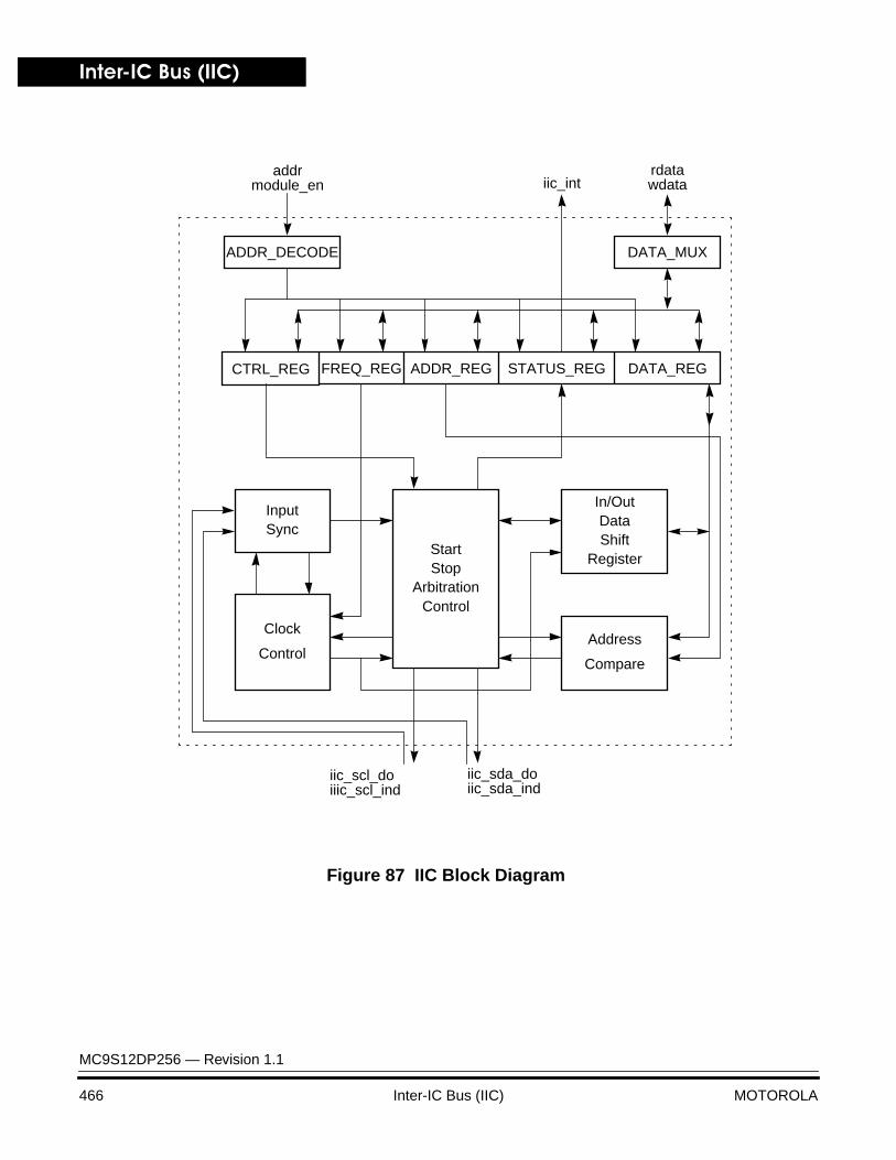
Inter-IC Bus (IIC)
MC9S12DP256 — Revision 1.1
466 Inter-IC Bus (IIC) MOTOROLA
Figure 87 IIC Block Diagram
InputSync
In/OutDataShift
Register
Address
Compare
iic_scl_do iic_sda_do
iic_intaddr rdata
Clock
Control
StartStop
ArbitrationControl
CTRL_REG FREQ_REG ADDR_REG STATUS_REG DATA_REG
ADDR_DECODE DATA_MUX
wdatamodule_en
iic_sda_indiiic_scl_ind
Inter-IC Bus (IIC)Signal Descriptions
MC9S12DP256 — Revision 1.1
MOTOROLA Inter-IC Bus (IIC) 467
Signal Descriptions
The IIC is a 16-bit module.
iic_scl_ind This is the unsynchronized SCL input from the pad.
iic_scl_do This is the SCL data output from the module.
iic_scl_port_en SCL pad enable signal. This signal is an output of the IIC and is made active when the IIC wants to control the SCL pad.
iic_scl_obe If the pad is controlled by the IIC, then this signal determines whether the IIC will drive iic_scl_do.
iic_sda_ind This is the unsynchronized SDA input from the pad.
iic_sda_do This is the SDA output from the module.
iic_sda_port_en SDA pad enable signal. This signal is an output of the IIC and is made active when the IIC wants to control the SDA pad.
Table 81 Signal Properties
Name Function
iic_scl_ind SCL input signal from pad
iic_scl_do SCL data output from module
iic_scl_port_en SCL enable signal
iic_scl_obe SCL input/output configure
iic_sda_ind SDA input signal from pad
iic_sda_do SDA data output from module
iic_sda_port_en SDA enable signal
iic_sda_obe SDA input/output configure
iic_int IIC interrupt signal
Inter-IC Bus (IIC)
MC9S12DP256 — Revision 1.1
468 Inter-IC Bus (IIC) MOTOROLA
iic_sda_obe If the pad is controlled by the IIC, then this signal determines whether the IIC will drive iic_sda_do.
Interrupt Signals The IIC has one interrupt signal iic_int. Refer to Section 6 of this document for the details regarding this signal.
Module Memory Map
The memory map for the IIC module is given below in Table 3-1. The Address listed for each register is the address offset. The total address for each register is the sum of the base address for the IIC module and the address offset for each register.
Table 82 Module Memory Map
Offset Use Access
$0000 IIC Address Register Read/Write
$0001 IIC Frequency Divider Register Read/Write
$0002 IIC Control Register Read/Write
$0003 IIC Status Register) Read/Write
$0004 IIC Data I/O Register Read/Write
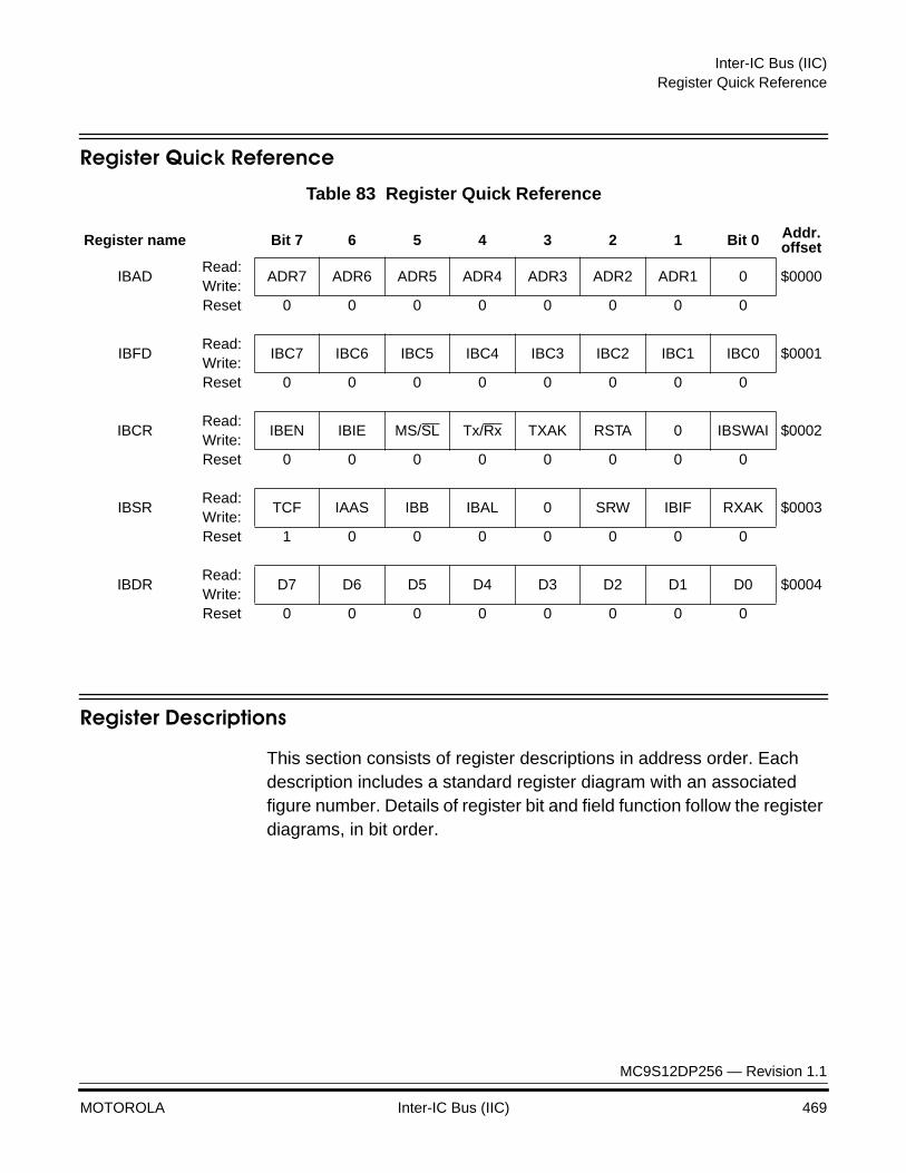
Inter-IC Bus (IIC)Register Quick Reference
MC9S12DP256 — Revision 1.1
MOTOROLA Inter-IC Bus (IIC) 469
Register Quick Reference
Register Descriptions
This section consists of register descriptions in address order. Each description includes a standard register diagram with an associated figure number. Details of register bit and field function follow the register diagrams, in bit order.
Table 83 Register Quick Reference
Register name Bit 7 6 5 4 3 2 1 Bit 0 Addr. offset
IBADRead:
ADR7 ADR6 ADR5 ADR4 ADR3 ADR2 ADR1 0 $0000Write:Reset 0 0 0 0 0 0 0 0
IBFDRead:
IBC7 IBC6 IBC5 IBC4 IBC3 IBC2 IBC1 IBC0 $0001Write:Reset 0 0 0 0 0 0 0 0
IBCRRead:
IBEN IBIE MS/SL Tx/Rx TXAK RSTA 0 IBSWAI $0002Write:Reset 0 0 0 0 0 0 0 0
IBSRRead:
TCF IAAS IBB IBAL 0 SRW IBIF RXAK $0003Write:Reset 1 0 0 0 0 0 0 0
IBDRRead:
D7 D6 D5 D4 D3 D2 D1 D0 $0004Write:Reset 0 0 0 0 0 0 0 0
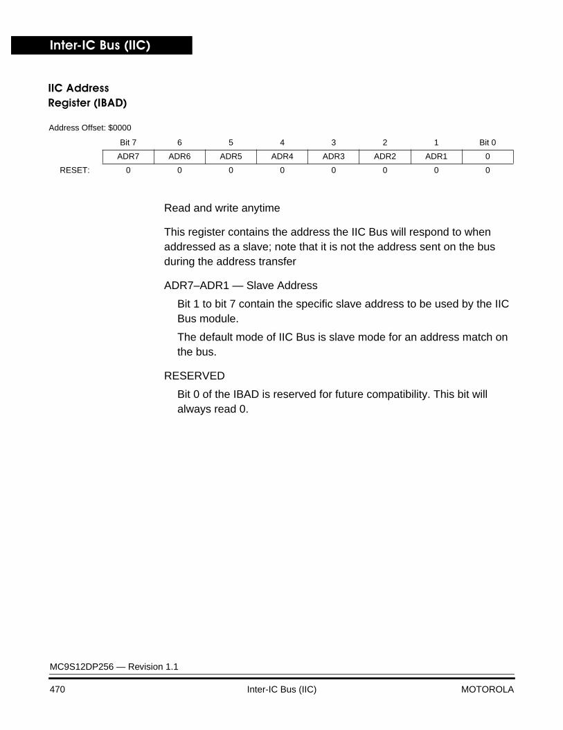
Inter-IC Bus (IIC)
MC9S12DP256 — Revision 1.1
470 Inter-IC Bus (IIC) MOTOROLA
IIC Address Register (IBAD)
Read and write anytime
This register contains the address the IIC Bus will respond to when addressed as a slave; note that it is not the address sent on the bus during the address transfer
ADR7–ADR1 — Slave Address
Bit 1 to bit 7 contain the specific slave address to be used by the IIC Bus module.
The default mode of IIC Bus is slave mode for an address match on the bus.
RESERVED
Bit 0 of the IBAD is reserved for future compatibility. This bit will always read 0.
Address Offset: $0000
Bit 7 6 5 4 3 2 1 Bit 0
ADR7 ADR6 ADR5 ADR4 ADR3 ADR2 ADR1 0
RESET: 0 0 0 0 0 0 0 0

Inter-IC Bus (IIC)Register Descriptions
MC9S12DP256 — Revision 1.1
MOTOROLA Inter-IC Bus (IIC) 471
IIC Frequency Divider Register (IBFD)
Read and write anytime
IBC7–IBC0 — I-Bus Clock Rate 7–0
This field is used to prescale the clock for bit rate selection. The bit clock generator is implemented as a prescale divider: IBC7–6 and IBC5–3 select the prescaler divider, and IBC2–0 select the shift register tap point. The IBC bits are decoded to give the Tap and Prescale values as shown in Table 84.
Address Offset: $0001
Bit 7 6 5 4 3 2 1 Bit 0
IBC7 IBC6 IBC5 IBC4 IBC3 IBC2 IBC1 IBC0
Reset: 0 0 0 0 0 0 0 0
Table 84 I-Bus Tap and Prescale Values
IBC2-0(bin)
SCL Tap(clocks)
SDA Tap(clocks)
000 5 1
001 6 1
010 7 2
011 8 2
100 9 3
101 10 3
110 12 4
111 15 4
IBC5-3(bin)
scl2tap(clocks)
tap2tap(clocks)
000 5 1
001 6 2
010 6 4
011 6 8
100 14 16
101 30 32
110 62 64
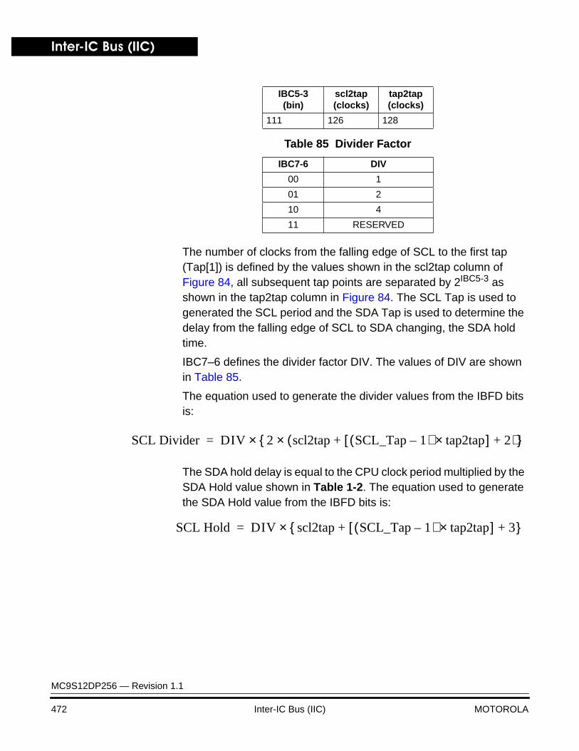
Inter-IC Bus (IIC)
MC9S12DP256 — Revision 1.1
472 Inter-IC Bus (IIC) MOTOROLA
The number of clocks from the falling edge of SCL to the first tap (Tap[1]) is defined by the values shown in the scl2tap column of Figure 84, all subsequent tap points are separated by 2IBC5-3 as shown in the tap2tap column in Figure 84. The SCL Tap is used to generated the SCL period and the SDA Tap is used to determine the delay from the falling edge of SCL to SDA changing, the SDA hold time.
IBC7–6 defines the divider factor DIV. The values of DIV are shown in Table 85.
The equation used to generate the divider values from the IBFD bits is:
The SDA hold delay is equal to the CPU clock period multiplied by the SDA Hold value shown in Table 1-2. The equation used to generate the SDA Hold value from the IBFD bits is:
111 126 128
Table 85 Divider Factor
IBC7-6 DIV
00 1
01 2
10 4
11 RESERVED
IBC5-3(bin)
scl2tap(clocks)
tap2tap(clocks)
SCL Divider DIV 2 scl2tap SCL_Tap 1–( ) tap2tap×[ ] 2+ +( )×{ }×=
SCL Hold DIV scl2tap SCL_Tap 1–( ) tap2tap×[ ] 3+ +{ }×=
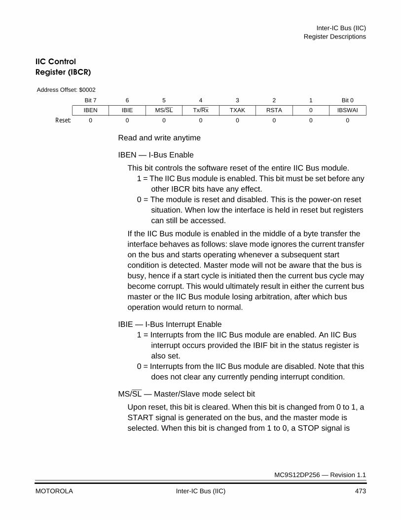
Inter-IC Bus (IIC)Register Descriptions
MC9S12DP256 — Revision 1.1
MOTOROLA Inter-IC Bus (IIC) 473
IIC Control Register (IBCR)
Read and write anytime
IBEN — I-Bus Enable
This bit controls the software reset of the entire IIC Bus module.1 = The IIC Bus module is enabled. This bit must be set before any
other IBCR bits have any effect.0 = The module is reset and disabled. This is the power-on reset
situation. When low the interface is held in reset but registers can still be accessed.
If the IIC Bus module is enabled in the middle of a byte transfer the interface behaves as follows: slave mode ignores the current transfer on the bus and starts operating whenever a subsequent start condition is detected. Master mode will not be aware that the bus is busy, hence if a start cycle is initiated then the current bus cycle may become corrupt. This would ultimately result in either the current bus master or the IIC Bus module losing arbitration, after which bus operation would return to normal.
IBIE — I-Bus Interrupt Enable1 = Interrupts from the IIC Bus module are enabled. An IIC Bus
interrupt occurs provided the IBIF bit in the status register is also set.
0 = Interrupts from the IIC Bus module are disabled. Note that this does not clear any currently pending interrupt condition.
MS/SL — Master/Slave mode select bit
Upon reset, this bit is cleared. When this bit is changed from 0 to 1, a START signal is generated on the bus, and the master mode is selected. When this bit is changed from 1 to 0, a STOP signal is
Address Offset: $0002
Bit 7 6 5 4 3 2 1 Bit 0
IBEN IBIE MS/SL Tx/Rx TXAK RSTA 0 IBSWAI
Reset: 0 0 0 0 0 0 0 0
Inter-IC Bus (IIC)
MC9S12DP256 — Revision 1.1
474 Inter-IC Bus (IIC) MOTOROLA
generated and the operation mode changes from master to slave.MS/SL is cleared without generating a STOP signal when the master loses arbitration.
1 = Master Mode0 = Slave Mode
Tx/Rx — Transmit/Receive mode select bit
This bit selects the direction of master and slave transfers. When addressed as a slave this bit should be set by software according to the SRW bit in the status register. In master mode this bit should be set according to the type of transfer required. Therefore, for address cycles, this bit will always be high.
1 = Transmit0 = Receive
TXAK — Transmit Acknowledge enable
This bit specifies the value driven onto SDA during data acknowledge cycles for both master and slave receivers. The IIC module will always acknowledge address matches, provided it is enabled, regardless of the value of TXAK. Note that values written to this bit are only used when the IIC Bus is a receiver, not a transmitter.
1 = No acknowledge signal response is sent (i.e., acknowledge bit = 1)
0 = An acknowledge signal will be sent out to the bus at the 9th clock bit after receiving one byte data
RSTA — Repeat Start
Writing a 1 to this bit will generate a repeated START condition on the bus, provided it is the current bus master. This bit will always be read as a low. Attempting a repeated start at the wrong time, if the bus is owned by another master, will result in loss of arbitration.
1 = Generate repeat start cycle
RESERVED
Bit 1 of the IBCR is reserved for future compatibility. This bit will always read 0.
IBSWAI — I-Bus Interface Stop in WAIT mode1 = Halt IIC Bus module clock generation in WAIT mode

Inter-IC Bus (IIC)Register Descriptions
MC9S12DP256 — Revision 1.1
MOTOROLA Inter-IC Bus (IIC) 475
0 = IIC Bus module clock operates normally
Wait mode is entered via execution of a CPU WAI instruction. In the event that the IBSWAI bit is set, all clocks internal to the IIC will be stopped and any transmission currently in progress will halt. If the CPU were woken up by a source other than the IIC module, then clocks would restart and the IIC would continue where it left off in the previous transmission. It is not possible for the IIC to wake up the CPU when its internal clocks are stopped.
If it were the case that the IBSWAI bit was cleared when the WAI instruction was executed, the IIC internal clocks and interface would remain alive, continuing the operation which was currently underway. It is also possible to configure the IIC such that it will wake up the CPU via an interrupt at the conclusion of the current operation. See the discussion on the IBIF and IBIE bits in the IBSR and IBCR, respectively.
IIC Status Register (IBSR)
This status register is read-only with exception of bit 1 (IBIF) and bit 4 (IBAL), which are software clearable
TCF — Data transferring bit
While one byte of data is being transferred, this bit is cleared. It is set by the falling edge of the 9th clock of a byte transfer. Note that this bit is only valid during or immediately following a transfer to the IIC module or from the IIC module.
1 = Transfer complete0 = Transfer in progress
Address Offset: $0003
Bit 7 6 5 4 3 2 1 Bit 0
TCF IAAS IBB IBAL 0 SRW IBIF RXAK
Reset: 1 0 0 0 0 0 0 0
Inter-IC Bus (IIC)
MC9S12DP256 — Revision 1.1
476 Inter-IC Bus (IIC) MOTOROLA
IAAS — Addressed as a slave bit
When its own specific address (I-Bus Address Register) is matched with the calling address, this bit is set. The CPU is interrupted provided the IBIE is set. Then the CPU needs to check the SRW bit and set its Tx/Rx mode accordingly. Writing to the I-Bus Control Register clears this bit.
1 = Addressed as a slave0 = Not addressed
IBB — Bus busy bit
This bit indicates the status of the bus. When a START signal is detected, the IBB is set. If a STOP signal is detected, it is cleared.
1 = Bus is busy0 = Bus is idle
IBAL — Arbitration Lost
The arbitration lost bit (IBAL) is set by hardware when the arbitration procedure is lost. Arbitration is lost in the following circumstances:
1. SDA sampled as a low when the master drives a high during an address or data transmit cycle.
2. SDA sampled as a low when the master drives a high during the acknowledge bit of a data receive cycle.
3. A start cycle is attempted when the bus is busy.
4. A repeated start cycle is requested in slave mode.
5. A stop condition is detected when the master did not request it.
This bit must be cleared by software, by writing a low to it.
RESERVED
Bit 3 of IBSR is reserved for future use. A read operation on this bit will return 0.

Inter-IC Bus (IIC)Register Descriptions
MC9S12DP256 — Revision 1.1
MOTOROLA Inter-IC Bus (IIC) 477
SRW — Slave Read/Write
When IAAS is set this bit indicates the value of the R/W command bit of the calling address sent from the master.
This bit is only valid when the I-Bus is in slave mode, a complete address transfer has occurred with an address match and no other transfers have been initiated.
Checking this bit, the CPU can select slave transmit/receive mode according to the command of the master.
1 = Slave transmit, master reading from slave0 = Slave receive, master writing to slave
IBIF — I-Bus Interrupt
The IBIF bit is set when an interrupt is pending, which will cause a processor interrupt request provided IBIE is set. IBIF is set when one of the following events occurs:
1. Complete one byte transfer (set at the falling edge of the 9th clock).
2. Receive a calling address that matches its own specific address in slave receive mode.
3. Arbitration lost.
This bit must be cleared by software, writing a low to it, in the interrupt routine.
RXAK — Received Acknowledge
The value of SDA during the acknowledge bit of a bus cycle. If the received acknowledge bit (RXAK) is low, it indicates an acknowledge signal has been received after the completion of 8 bits data transmission on the bus. If RXAK is high, it means no acknowledge signal is detected at the 9th clock.
1 = No acknowledge received0 = Acknowledge received

Inter-IC Bus (IIC)
MC9S12DP256 — Revision 1.1
478 Inter-IC Bus (IIC) MOTOROLA
IIC Data I/O Register (IBDR)
In master transmit mode, when data is written to the IBDR a data transfer is initiated. The most significant bit is sent first. In master receive mode, reading this register initiates next byte data receiving. In slave mode, the same functions are available after an address match has occurred. Note that the Tx/Rx bit in the IBCR must correctly reflect the desired direction of transfer in master and slave modes for the transmission to begin. For instance, if the IIC is configured for master transmit but a master receive is desired, then reading the IBDR will not initiate the receive.
Reading the IBDR will return the last byte received while the IIC is configured in either master receive or slave receive modes. The IBDR does not reflect every byte that is transmitted on the IIC bus, nor can software verify that a byte has been written to the IBDR correctly by reading it back.
In master transmit mode, the first byte of data written to IBDR following assertion of MS/SL is used for the address transfer and should comprise of the calling address (in position D7-D1) concatenated with the required R/W bit (in position D0).
I-Bus Protocol
The IIC Bus system uses a Serial Data line (SDA) and a Serial Clock Line (SCL) for data transfer. All devices connected to it must have open drain or open collector outputs. Logic AND function is exercised on both lines with external pull-up resistors, the value of these resistors is system dependent.
Address Offset: $0004
Bit 7 6 5 4 3 2 1 Bit 0
D7 D6 D5 D4 D3 D2 D1 D0
Reset: 0 0 0 0 0 0 0 0
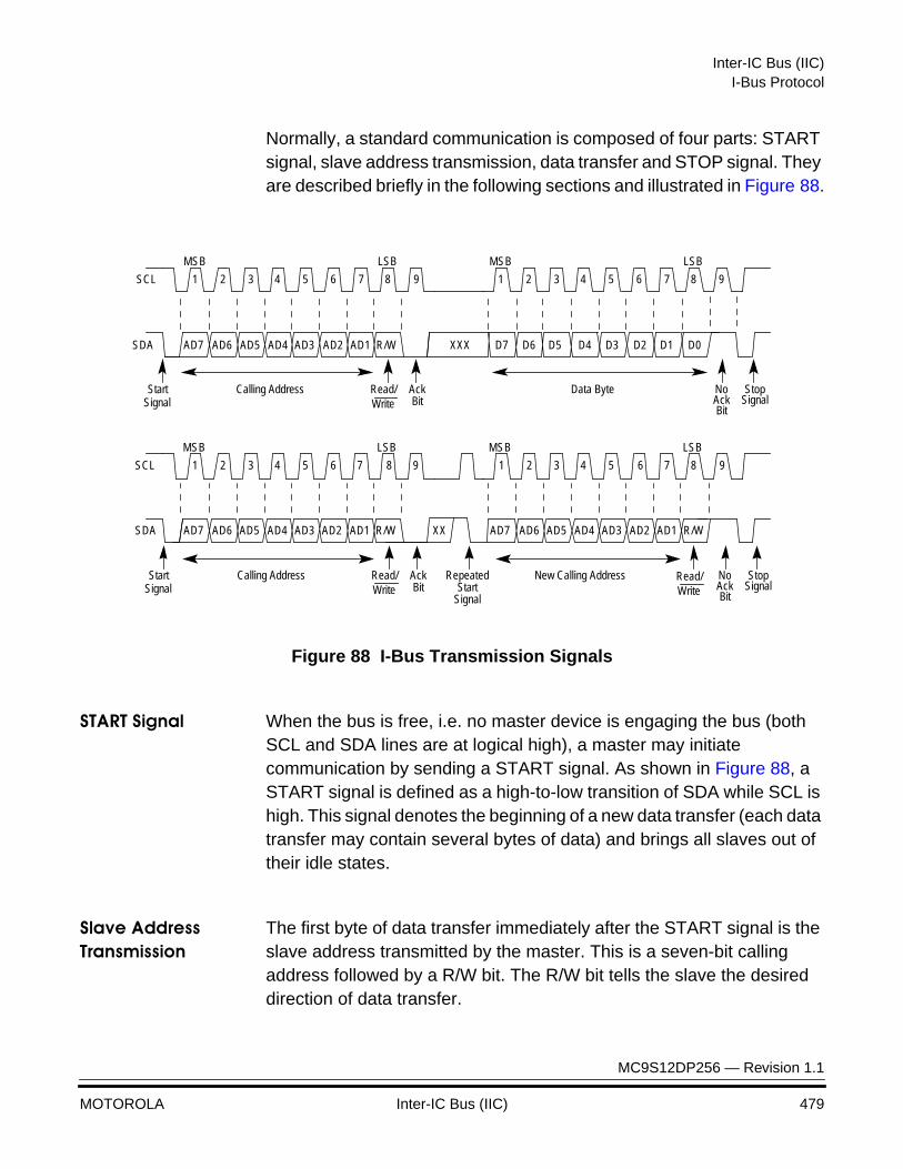
Inter-IC Bus (IIC)I-Bus Protocol
MC9S12DP256 — Revision 1.1
MOTOROLA Inter-IC Bus (IIC) 479
Normally, a standard communication is composed of four parts: START signal, slave address transmission, data transfer and STOP signal. They are described briefly in the following sections and illustrated in Figure 88.
Figure 88 I-Bus Transmission Signals
START Signal When the bus is free, i.e. no master device is engaging the bus (both SCL and SDA lines are at logical high), a master may initiate communication by sending a START signal. As shown in Figure 88, a START signal is defined as a high-to-low transition of SDA while SCL is high. This signal denotes the beginning of a new data transfer (each data transfer may contain several bytes of data) and brings all slaves out of their idle states.
Slave Address Transmission
The first byte of data transfer immediately after the START signal is the slave address transmitted by the master. This is a seven-bit calling address followed by a R/W bit. The R/W bit tells the slave the desired direction of data transfer.
SCL
SDA
StartSignal
AckBit
1 2 3 4 5 6 7 8
MSB LSB
1 2 3 4 5 6 7 8
MSB LSB
StopSignal
No
SCL
SDA
1 2 3 4 5 6 7 8
MSB LSB
1 2 5 6 7 8
MSB LSB
Repeated
3 4
9 9
AD7 AD6 AD5 AD4 AD3 AD2 AD1 R/W XXX D7 D6 D5 D4 D3 D2 D1 D0
Calling Address Read/ Data Byte
AD7 AD6 AD5 AD4 AD3 AD2 AD1 R/W AD7 AD6 AD5 AD4 AD3 AD2 AD1 R/W
New Calling Address
9 9
XX
AckBitWrite
StartSignal
StartSignal
AckBit
Calling Address Read/Write
StopSignal
NoAckBit
Read/Write

Inter-IC Bus (IIC)
MC9S12DP256 — Revision 1.1
480 Inter-IC Bus (IIC) MOTOROLA
1 = Read transfer, the slave transmits data to the master.0 = Write transfer, the master transmits data to the slave.
Only the slave with a calling address that matches the one transmitted by the master will respond by sending back an acknowledge bit. This is done by pulling the SDA low at the 9th clock (see Figure 88).
No two slaves in the system may have the same address. If the IIC Bus is master, it must not transmit an address that is equal to its own slave address. The IIC Bus cannot be master and slave at the same time. However, if arbitration is lost during an address cycle the IIC Bus will revert to slave mode and operate correctly even if it is being addressed by another master.
Data Transfer Once successful slave addressing is achieved, the data transfer can proceed byte-by-byte in a direction specified by the R/W bit sent by the calling master.
All transfers that come after an address cycle are referred to as data transfers, even if they carry sub-address information for the slave device.
Each data byte is 8 bits long. Data may be changed only while SCL is low and must be held stable while SCL is high as shown in Figure 88. There is one clock pulse on SCL for each data bit, the MSB being transferred first. Each data byte has to be followed by an acknowledge bit, which is signalled from the receiving device by pulling the SDA low at the ninth clock. So one complete data byte transfer needs nine clock pulses.
If the slave receiver does not acknowledge the master, the SDA line must be left high by the slave. The master can then generate a stop signal to abort the data transfer or a start signal (repeated start) to commence a new calling.
If the master receiver does not acknowledge the slave transmitter after a byte transmission, it means ‘end of data’ to the slave, so the slave releases the SDA line for the master to generate STOP or START signal.
Inter-IC Bus (IIC)I-Bus Protocol
MC9S12DP256 — Revision 1.1
MOTOROLA Inter-IC Bus (IIC) 481
STOP Signal The master can terminate the communication by generating a STOP signal to free the bus. However, the master may generate a START signal followed by a calling command without generating a STOP signal first. This is called repeated START. A STOP signal is defined as a low-to-high transition of SDA while SCL at logical “1” (see Figure 88).
The master can generate a STOP even if the slave has generated an acknowledge at which point the slave must release the bus.
Repeated START Signal
As shown in Figure 88, a repeated START signal is a START signal generated without first generating a STOP signal to terminate the communication. This is used by the master to communicate with another slave or with the same slave in different mode (transmit/receive mode) without releasing the bus.
Arbitration Procedure
The Inter-IC bus is a true multi-master bus that allows more than one master to be connected on it. If two or more masters try to control the bus at the same time, a clock synchronization procedure determines the bus clock, for which the low period is equal to the longest clock low period and the high is equal to the shortest one among the masters. The relative priority of the contending masters is determined by a data arbitration procedure, a bus master loses arbitration if it transmits logic “1” while another master transmits logic “0”. The losing masters immediately switch over to slave receive mode and stop driving SDA output. In this case the transition from master to slave mode does not generate a STOP condition. Meanwhile, a status bit is set by hardware to indicate loss of arbitration.
Clock Synchronization
Since wire-AND logic is performed on SCL line, a high-to-low transition on SCL line affects all the devices connected on the bus. The devices start counting their low period and once a device's clock has gone low, it holds the SCL line low until the clock high state is reached. However, the change of low to high in this device clock may not change the state of the SCL line if another device clock is still within its low period. Therefore, synchronized clock SCL is held low by the device with the longest low period. Devices with shorter low periods enter a high wait

Inter-IC Bus (IIC)
MC9S12DP256 — Revision 1.1
482 Inter-IC Bus (IIC) MOTOROLA
state during this time (see Figure 89). When all devices concerned have counted off their low period, the synchronized clock SCL line is released and pulled high. There is then no difference between the device clocks and the state of the SCL line and all the devices start counting their high periods. The first device to complete its high period pulls the SCL line low again.
Figure 89 I-Bus Clock Synchronization
Handshaking The clock synchronization mechanism can be used as a handshake in data transfer. Slave devices may hold the SCL low after completion of one byte transfer (9 bits). In such case, it halts the bus clock and forces the master clock into wait states until the slave releases the SCL line.
Clock Stretching The clock synchronization mechanism can be used by slaves to slow down the bit rate of a transfer. After the master has driven SCL low the slave can drive SCL low for the required period and then release it. If the slave SCL low period is greater than the master SCL low period then the resulting SCL bus signal low period is stretched.
SCL1
SCL2
SCL
Internal Counter Reset
WAIT Start Counting High Period

Inter-IC Bus (IIC)Interrupt Operation
MC9S12DP256 — Revision 1.1
MOTOROLA Inter-IC Bus (IIC) 483
Interrupt Operation
System Level Interrupt Sources
There is one interrupt signal that is sent from the IIC to the core.
Interrupt Descriptions
See the Interrupts section of the End User Guide, which describes the Interrupt signals generated by the IIC Status registers.
Internally there are three types of interrupts. These are generated on
1. Arbitration Lost Interrupt
2. Byte Transfer Interrupt
3. Address Detect Interrupt
There is only one interrupt signal iic_int to core. The interrupt is driven by Bit IBIF (of the IIC Status Register) and masked with bit IBIE (of the IIC Control Register). This bit must be cleared by software by writing a low to it in the interrupt routine. core can determine the Interrupt type after reading the Status Register.
Arbitration Lost Interrupt
The Inter-IC bus is a true multi-master bus that allows more than one master to be connected on it. If two or more masters try to control the bus at the same time, the relative priority of the contending masters is determined by a data arbitration procedure. The IIC module asserts this interrupt when It loses the data arbitration process. And IBAL bit in Status Register is also set.
Arbitration is lost in the following circumstances:
1. SDA sampled as a low when the master drives a high during an address or data transmit cycle.
2. SDA sampled as a low when the master drives a high during the acknowledge bit of a data receive cycle.
3. A start cycle is attempted when the bus is busy.
4. A repeated start cycle is requested in slave mode.
5. A stop condition is detected when the master did not request it.
Inter-IC Bus (IIC)
MC9S12DP256 — Revision 1.1
484 Inter-IC Bus (IIC) MOTOROLA
This bit must be cleared by software, by writing a low to it.
Byte Transfer Interrupt
After completion of byte transfer, TCF (Data Transfer) bit is set at the falling edge of the 9th clock to indicate the completion of Byte Transfer.
Address Detect Interrupt
When its own specific address (I-Bus Address Register) is matched with the calling address, IAAS bit in Status register is set. The CPU is interrupted provided the IBIE is set. Then the CPU needs to check the SRW bit and set its Tx/Rx mode accordingly.
Modes of Operation
The IIC functions the same in normal, special, and emulation modes. It has two low power modes, wait and stop modes.
Run Mode This is the basic mode of operation.
Wait Mode IIC operation in wait mode is a configurable low power mode. Depending on the state of internal bits, the IIC can operate normally when the CPU is in wait mode or the IIC clock generation can be turned off and the IIC module enters a power conservation state during wait mode. In the later case, any transmission or reception in progress stops at wait mode entry.
Stop Mode The IIC is inactive in stop mode for reduced power consumption. The STOP instruction does not affect IIC register states.
Inter-IC Bus (IIC)Programming
MC9S12DP256 — Revision 1.1
MOTOROLA Inter-IC Bus (IIC) 485
Programming
Initialization Sequence
Reset will put the IIC Control Register to its default status. Before the interface can be used to transfer serial data, an initialization procedure must be carried out, as follows:
1. Update the Frequency Divider Register (IBFD) and select the required division ratio to obtain SCL frequency from system clock.
2. Update the IIC Address Register (IBAD) to define its slave address.
3. Set the IBEN bit of the IIC Control Register (IBCR) to enable the IIC system.
4. Modify the bits of the IIC Control Register (IBCR) to select Master/Slave mode, Transmit/Receive mode and interrupt enable or not.
Generation of START
After completion of the initialization procedure, serial data can be transmitted by selecting the ‘master transmitter’ mode. If the device is connected to a multi-master bus system, the state of the IIC Busy Bit (IBB) must be tested to check whether the serial bus is free.
If the bus is free (IBB=0), the start condition and the first byte (the slave address) can be sent. The data written to the data register comprises the slave calling address and the LSB set to indicate the direction of transfer required from the slave.
The bus free time (i.e., the time between a STOP condition and the following START condition) is built into the hardware that generates the START cycle. Depending on the relative frequencies of the system clock and the SCL period it may be necessary to wait until the IIC is busy after writing the calling address to the IBDR before proceeding with the following instructions. This is illustrated in the following example.
Inter-IC Bus (IIC)
MC9S12DP256 — Revision 1.1
486 Inter-IC Bus (IIC) MOTOROLA
An example of a program which generates the START signal and transmits the first byte of data (slave address) is shown below:
Post-Transfer Software Response
Transmission or reception of a byte by the IIC will set the data transferring bit (TCF) to 1, which indicates one byte communication is finished. The IIC interrupt bit (IBIF) is set also; an interrupt will be generated if the interrupt function is enabled during initialization by setting the IBIE bit. Software must clear the IBIF bit in the interrupt routine first. The TCF bit will be cleared by reading from the IIC Data I/O Register (IBDR) in receive mode or writing to IBDR in transmit mode.
Software may service the IIC I/O in the main program by monitoring the IBIF bit if the interrupt function is disabled. Note that polling should monitor the IBIF bit rather than the TCF bit since their operation is different when arbitration is lost.
Note that when an interrupt occurs at the end of the address cycle the master will always be in transmit mode, i.e. the address is transmitted. If master receive mode is required, indicated by R/W bit in IBDR, then the Tx/Rx bit should be toggled at this stage.
During slave mode address cycles (IAAS=1) the SRW bit in the status register is read to determine the direction of the subsequent transfer and the Tx/Rx bit is programmed accordingly. For slave mode data cycles (IAAS=0) the SRW bit is not valid, the Tx/Rx bit in the control register should be read to determine the direction of the current transfer.
The following is an example of a software response by a ‘master transmitter’ in the interrupt routine (see Figure 90).
CHFLAG BRSET IBSR,#$20, * ;WAIT FOR IBB FLAG TO CLEARTXSTART BSET IBCR,#$30 ;SET TRANSMIT AND MASTER MODE
;i.e. GENERATE START CONDITIONMOVEB CALLING,IBDR ;TRANSMIT THE CALLING
;ADDRESS, D0=R/WIBFREE BRCLR #5,IBSR,#$20,* ;WAIT FOR IBB FLAG TO SET
Inter-IC Bus (IIC)Programming
MC9S12DP256 — Revision 1.1
MOTOROLA Inter-IC Bus (IIC) 487
Generation of STOP
A data transfer ends with a STOP signal generated by the ‘master’ device. A master transmitter can simply generate a STOP signal after all the data has been transmitted. The following is an example showing how a stop condition is generated by a master transmitter.
If a master receiver wants to terminate a data transfer, it must inform the slave transmitter by not acknowledging the last byte of data which can be done by setting the transmit acknowledge bit (TXAK) before reading the 2nd last byte of data. Before reading the last byte of data, a STOP signal must be generated first. The following is an example showing how a STOP signal is generated by a master receiver.
ISR BCLR IBSR,#$02 ;CLEAR THE IBIF FLAGBRCLR IBCR,#$20,SLAVE ;BRANCH IF IN SLAVE MODEBRCLR IBCR,#$10,RECEIVE ;BRANCH IF IN RECEIVE MODEBRSET IBSR,#$01,END ;IF NO ACK, END OF TRANSMISSION
TRANSMIT MOVB DATABUF,IBDR ;TRANSMIT NEXT BYTE OF DATA
MASTX TST TXCNT ;GET VALUE FROM THE ;TRANSMITING COUNTER
BEQ END ;END IF NO MORE DATABRSET IBSR,#$01,END ;END IF NO ACKMOVB DATABUF,IBDR ;TRANSMIT NEXT BYTE OF DATADEC TXCNT ;DECREASE THE TXCNTBRA EMASTX ;EXIT
END BCLR IBCR,#$20 ;GENERATE A STOP CONDITIONEMASTX RTI ;RETURN FROM INTERRUPT
MASR DEC RXCNT ;DECREASE THE RXCNTBEQ ENMASR ;LAST BYTE TO BE READMOVB RXCNT,D1 ;CHECK SECOND LAST BYTEDEC D1 ;TO BE READBNE NXMAR ;NOT LAST OR SECOND LAST
LAMAR BSET IBCR,#$08 ;SECOND LAST, DISABLE ACK ;TRANSMITTING
BRA NXMARENMASR BCLR IBCR,#$20 ;LAST ONE, GENERATE ‘STOP’ SIGNALNXMAR MOVB IBDR,RXBUF ;READ DATA AND STORE
RTI
Inter-IC Bus (IIC)
MC9S12DP256 — Revision 1.1
488 Inter-IC Bus (IIC) MOTOROLA
Generation of Repeated START
At the end of data transfer, if the master still wants to communicate on the bus, it can generate another START signal followed by another slave address without first generating a STOP signal. A program example is as shown.
Slave Mode In the slave interrupt service routine, the module addressed as slave bit (IAAS) should be tested to check if a calling of its own address has just been received (see Figure 90). If IAAS is set, software should set the transmit/receive mode select bit (Tx/Rx bit of IBCR) according to the R/W command bit (SRW). Writing to the IBCR clears the IAAS automatically. Note that the only time IAAS is read as set is from the interrupt at the end of the address cycle where an address match occurred, interrupts resulting from subsequent data transfers will have IAAS cleared. A data transfer may now be initiated by writing information to IBDR, for slave transmits, or dummy reading from IBDR, in slave receive mode. The slave will drive SCL low in-between byte transfers, SCL is released when the IBDR is accessed in the required mode.
In slave transmitter routine, the received acknowledge bit (RXAK) must be tested before transmitting the next byte of data. Setting RXAK means an ‘end of data’ signal from the master receiver, after which it must be switched from transmitter mode to receiver mode by software. A dummy read then releases the SCL line so that the master can generate a STOP signal.
RESTART BSET IBCR,#$04 ANOTHER START (RESTART)MOVB CALLING,IBDR ;TRANSMIT THE CALLING ADDRESS
;D0=R/W
Inter-IC Bus (IIC)Programming
MC9S12DP256 — Revision 1.1
MOTOROLA Inter-IC Bus (IIC) 489
Arbitration Lost If several masters try to engage the bus simultaneously, only one master wins and the others lose arbitration. The devices which lost arbitration are immediately switched to slave receive mode by the hardware. Their data output to the SDA line is stopped, but SCL is still generated until the end of the byte during which arbitration was lost. An interrupt occurs at the falling edge of the ninth clock of this transfer with IBAL=1 and MS/SL=0. If one master attempts to start transmission while the bus is being engaged by another master, the hardware will inhibit the transmission; switch the MS/SL bit from 1 to 0 without generating STOP condition; generate an interrupt to CPU and set the IBAL to indicate that the attempt to engage the bus is failed. When considering these cases, the slave service routine should test the IBAL first and the software should clear the IBAL bit if it is set.

Inter-IC Bus (IIC)
MC9S12DP256 — Revision 1.1
490 Inter-IC Bus (IIC) MOTOROLA
Figure 90 Flow-Chart of Typical I-Bus Interrupt Routine
Clear
Master Mode
?
Tx/Rx ?
Last Byte Transmitted
?
RXAK=0 ?
End Of Addr Cycle (Master Rx)
?
Write NextByte To IBDR
Switch To Rx Mode
Dummy Read From IBDR
Generate Stop Signal
Read Data From IBDR And Store
Set TXAK =1 Generate Stop Signal
2nd Last Byte To Be Read
?
Last Byte To Be Read
?
Arbitration Lost
?
Clear IBAL
IAAS=1 ?
IAAS=1 ?
SRW=1 ?
TX/RX ?
Set TX Mode
Write Data To IBDR
Set RX Mode
Dummy Read From IBDR
ACK FromReceiver
?
Tx Next Byte
Read Data From IBDR And Store
Switch To Rx Mode
Dummy Read From IBDR
RTI
Y N
Y
Y Y
Y
Y
Y
Y
Y
Y
N
N
N
NN
N
N
N
N
Y
TX RX
RX
TX(Write)
(Read)
N
IBIF
Address Transfer Data Transfer
MC9S12DP256 — Revision 1.1
MOTOROLA MSCAN 491
MSCANMSCAN
Contents
Overview . . . . . . . . . . . . . . . . . . . . . . . . . . . . . . . . . . . . . . . . . . . . . . 491Features . . . . . . . . . . . . . . . . . . . . . . . . . . . . . . . . . . . . . . . . . . . . . . 492Block Diagram. . . . . . . . . . . . . . . . . . . . . . . . . . . . . . . . . . . . . . . . . . 493External Pin Descriptions . . . . . . . . . . . . . . . . . . . . . . . . . . . . . . . . . 494Register Map. . . . . . . . . . . . . . . . . . . . . . . . . . . . . . . . . . . . . . . . . . . 496Functional Description. . . . . . . . . . . . . . . . . . . . . . . . . . . . . . . . . . . . 499Register Descriptions . . . . . . . . . . . . . . . . . . . . . . . . . . . . . . . . . . . . 512Modes of Operation. . . . . . . . . . . . . . . . . . . . . . . . . . . . . . . . . . . . . . 546Low Power Options . . . . . . . . . . . . . . . . . . . . . . . . . . . . . . . . . . . . . . 547Interrupt Operation . . . . . . . . . . . . . . . . . . . . . . . . . . . . . . . . . . . . . . 553
Overview
The Motorola Scalable Controller Area Network (MSCAN) definition is based on the MSCAN12 definition which is the specific implementation of the Motorola Scalable CAN concept targeted for the Motorola MC68HC12 Microcontroller Family.
The module is a communication controller implementing the CAN 2.0 A/B protocol as defined in the BOSCH specification dated September 1991. For users to fully understand the MSCAN specification, it is recommended that the Bosch specification be read first to familiarize the reader with the terms and concepts contained within this document.
The CAN protocol was primarily, but not only, designed to be used as a vehicle serial data bus, meeting the specific requirements of this field: real-time processing, reliable operation in the EMI environment of a vehicle, cost-effectiveness and required bandwidth.
MSCAN
MC9S12DP256 — Revision 1.1
492 MSCAN MOTOROLA
MSCAN utilizes an advanced buffer arrangement resulting in a predictable real-time behavior and simplifies the application software.
Features
The basic features of the MSCAN are as follows:
• Modular architecture
• Implementation of the CAN protocol – Version 2.0A/B
– Standard and extended data frames
– 0–8 bytes data length
– Programmable bit rate up to 1 Mbps1
– Support for remote frames
• 4 receive buffers with FIFO storage scheme
• 3 transmit buffers with internal prioritization using a ‘local priority’ concept
• Flexible maskable identifier filter supports two full size extended identifier filters (two 32-bit) or four 16-bit filters or eight 8-bit filters
• Programmable wake-up functionality with integrated low-pass filter
• Programmable loop back mode supports self-test operation
• Programmable listen-only mode for monitoring of CAN bus
• Separate signalling and interrupt capabilities for all CAN receiver and transmitter error states (Warning, Error Passive, Bus-Off)
• Programmable MSCAN clock source either system clock or crystal oscillator output
• Internal timer for time-stamping of received and transmitted messages
• Three low power modes: Sleep, Power Down and MSCAN Enable
1. Depending on the actual bit timing and the clock jitter of the PLL.
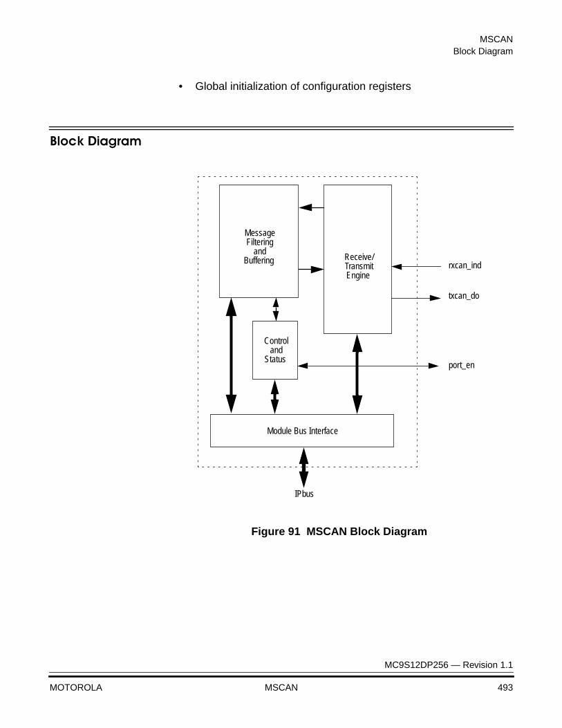
MSCANBlock Diagram
MC9S12DP256 — Revision 1.1
MOTOROLA MSCAN 493
• Global initialization of configuration registers
Block Diagram
Figure 91 MSCAN Block Diagram
port_en
rxcan_ind
txcan_do
Receive/
IPbus
TransmitEngine
MessageFiltering
andBuffering
Controland
Status
Module Bus Interface

MSCAN
MC9S12DP256 — Revision 1.1
494 MSCAN MOTOROLA
External Pin Descriptions
The MSCAN uses 2 external pins, 1 input (RxCAN) and 1 output (TxCAN). The TxCAN output pin represents the logic level on the CAN:
• ‘0’ is for a dominant state
• ‘1’ is for a recessive state
When the MSCAN is enabled (CANE=1) via the CANCTL1 register, the TxCAN and RxCAN pins will be enabled within the Port Module. This is indicated to Port Module using a dedicated enable line (ipp_port_en). When the MSCAN is disabled (CANE=0), these pins are available as general purpose I/O in the Port Module
A typical CAN system with MSCAN is shown in Figure 92. Each CAN station is connected physically to the CAN bus lines through a transceiver chip. The transceiver is capable of driving the large current needed for the CAN bus and has current protection against defected CAN or defected stations.
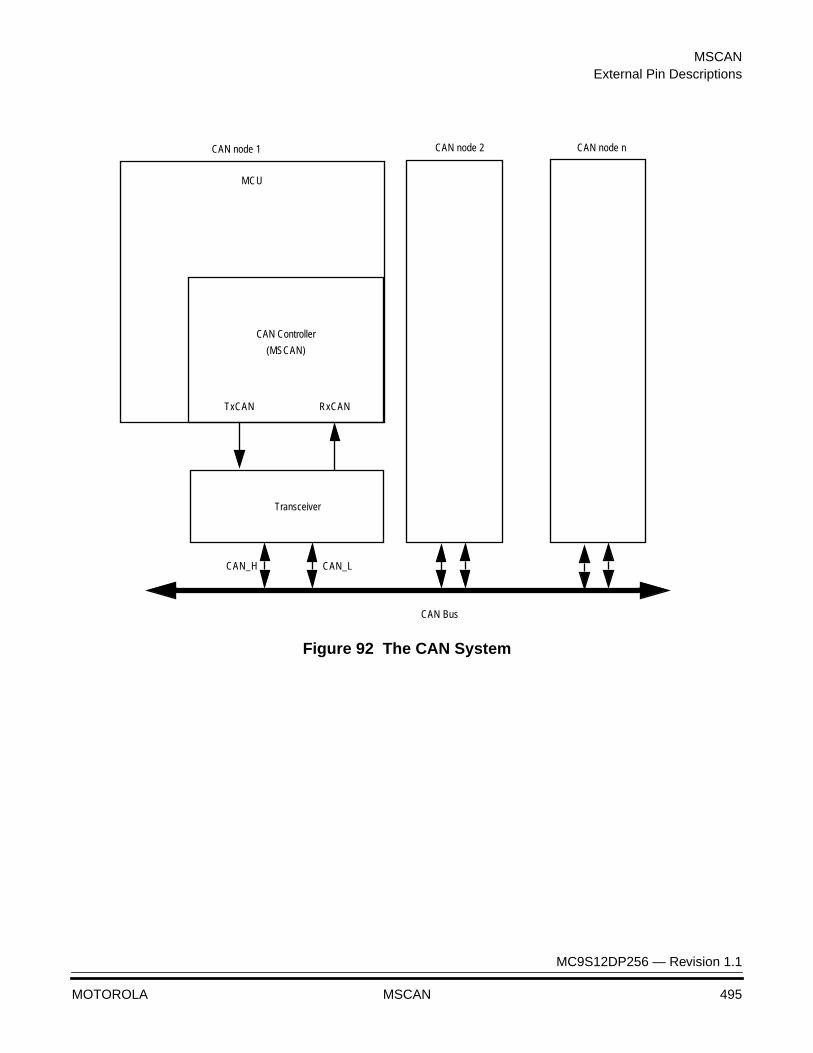
MSCANExternal Pin Descriptions
MC9S12DP256 — Revision 1.1
MOTOROLA MSCAN 495
Figure 92 The CAN System
CAN Bus
CAN Controller
(MSCAN)
Transceiver
CAN node 1 CAN node 2 CAN node n
CAN_LCAN_H
TxCAN RxCAN
MCU
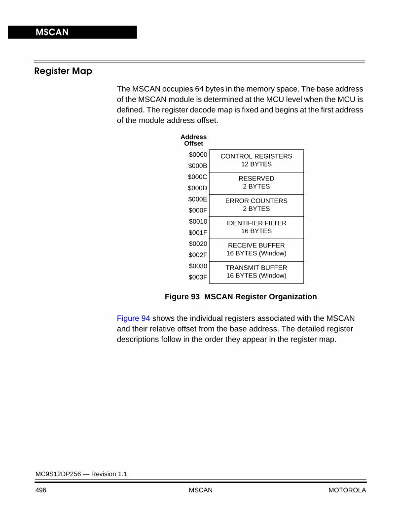
MSCAN
MC9S12DP256 — Revision 1.1
496 MSCAN MOTOROLA
Register Map
The MSCAN occupies 64 bytes in the memory space. The base address of the MSCAN module is determined at the MCU level when the MCU is defined. The register decode map is fixed and begins at the first address of the module address offset.
Figure 93 MSCAN Register Organization
Figure 94 shows the individual registers associated with the MSCAN and their relative offset from the base address. The detailed register descriptions follow in the order they appear in the register map.
Address Offset
$0000 CONTROL REGISTERS12 BYTES$000B
$000C RESERVED2 BYTES$000D
$000E ERROR COUNTERS2 BYTES$000F
$0010 IDENTIFIER FILTER16 BYTES$001F
$0020 RECEIVE BUFFER16 BYTES (Window)$002F
$0030 TRANSMIT BUFFER16 BYTES (Window)$003F

MSCANRegister Map
MC9S12DP256 — Revision 1.1
MOTOROLA MSCAN 497
Reserved bits within a register always read as 0 and a write is unimplemented1. Unimplemented functions are indicated by shading the bit.
1. Reserved bits within the Tx- & Rx-Buffers (CANTXFG, CANRXFG) will be read as ‘X’, because of RAM based implementation.
Register name Bit 7 6 5 4 3 2 1 Bit 0 Addr.Offset
CANCTL0Read:
RXFRMRXACT
CSWAISYNCH
TIME WUPE SLPRQ INITRQ $0000Write:
CANCTL1Read:
CANE CLKSRC LOOPB LISTEN0
WUPMSLPAK INITAK
$0001Write:
CANBTR0Read:
SJW1 SJW0 BRP5 BRP4 BRP3 BRP2 BRP1 BRP0 $0002Write:
CANBTR1Read:
SAMP TSEG22 TSEG21 TSEG20 TSEG13 TSEG12 TSEG11 TSEG10 $0003Write:
CANRFLGRead:
WUPIF CSCIFRSTAT1 RSTAT0 TSTAT1 TSTAT0
OVRIF RXF $0004Write:
CANRIERRead:
WUPIE CSCIE RSTATE1 RSTATE0 TSTATE1 TSTATE0 OVRIE RXFIE $0005Write:
CANTFLGRead: 0 0 0 0 0
TXE2 TXE1 TXE0 $0006Write:
CANTIERRead: 0 0 0 0 0
TXEIE2 TXEIE1 TXEIE0 $0007Write:
CANTARQRead: 0 0 0 0 0
ABTRQ2 ABTRQ1 ABTRQ0 $0008Write:
CANTAAKRead: 0 0 0 0 0 ABTAK2 ABTAK1 ABTAK0
$0009Write:
CANTBSELRead: 0 0 0 0 0
TX2 TX1 TX0 $000AWrite:
CANIDACRead: 0 0
IDAM1 IDAM00 IDHIT2 IDHIT1 IDHIT0
$000BWrite:
RESERVEDRead: 0 0 0 0 0 0 0 0 $000C
-$000D Write:
CANRXERRRead: RXERR7 RXERR6 RXERR5 RXERR4 RXERR3 RXERR2 RXERR1 RXERR0
$000EWrite:
CANTXERRRead: TXERR7 TXERR6 TXERR5 TXERR4 TXERR3 TXERR2 TXERR1 TXERR0
$000FWrite:
CANIDAR0Read:
AC7 AC6 AC5 AC4 AC3 AC2 AC1 AC0 $0010Write:
= Unimplemented
Figure 94 MSCAN Register Map
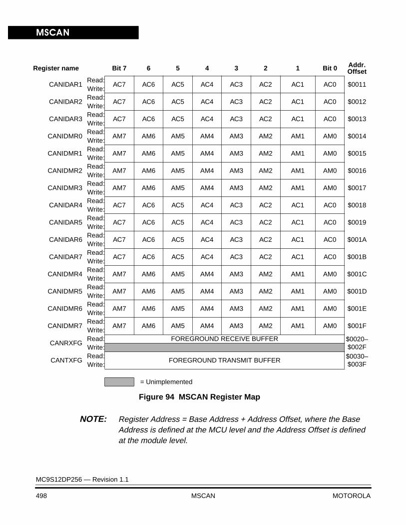
MSCAN
MC9S12DP256 — Revision 1.1
498 MSCAN MOTOROLA
NOTE: Register Address = Base Address + Address Offset, where the Base Address is defined at the MCU level and the Address Offset is defined at the module level.
CANIDAR1Read:
AC7 AC6 AC5 AC4 AC3 AC2 AC1 AC0 $0011Write:
CANIDAR2Read:
AC7 AC6 AC5 AC4 AC3 AC2 AC1 AC0 $0012Write:
CANIDAR3Read:
AC7 AC6 AC5 AC4 AC3 AC2 AC1 AC0 $0013Write:
CANIDMR0Read:
AM7 AM6 AM5 AM4 AM3 AM2 AM1 AM0 $0014Write:
CANIDMR1Read:
AM7 AM6 AM5 AM4 AM3 AM2 AM1 AM0 $0015Write:
CANIDMR2Read:
AM7 AM6 AM5 AM4 AM3 AM2 AM1 AM0 $0016Write:
CANIDMR3Read:
AM7 AM6 AM5 AM4 AM3 AM2 AM1 AM0 $0017Write:
CANIDAR4Read:
AC7 AC6 AC5 AC4 AC3 AC2 AC1 AC0 $0018Write:
CANIDAR5Read:
AC7 AC6 AC5 AC4 AC3 AC2 AC1 AC0 $0019Write:
CANIDAR6Read:
AC7 AC6 AC5 AC4 AC3 AC2 AC1 AC0 $001AWrite:
CANIDAR7Read:
AC7 AC6 AC5 AC4 AC3 AC2 AC1 AC0 $001BWrite:
CANIDMR4Read:
AM7 AM6 AM5 AM4 AM3 AM2 AM1 AM0 $001CWrite:
CANIDMR5Read:
AM7 AM6 AM5 AM4 AM3 AM2 AM1 AM0 $001DWrite:
CANIDMR6Read:
AM7 AM6 AM5 AM4 AM3 AM2 AM1 AM0 $001EWrite:
CANIDMR7Read:
AM7 AM6 AM5 AM4 AM3 AM2 AM1 AM0 $001FWrite:
CANRXFGRead: FOREGROUND RECEIVE BUFFER $0020–
$002FWrite:
CANTXFGRead:
FOREGROUND TRANSMIT BUFFER$0030–$003FWrite:
Register name Bit 7 6 5 4 3 2 1 Bit 0 Addr.Offset
= Unimplemented
Figure 94 MSCAN Register Map
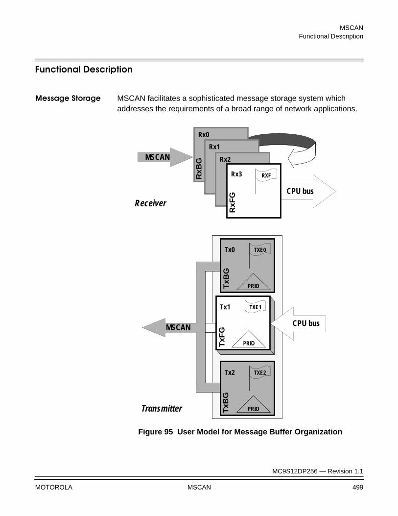
MSCANFunctional Description
MC9S12DP256 — Revision 1.1
MOTOROLA MSCAN 499
Functional Description
Message Storage MSCAN facilitates a sophisticated message storage system which addresses the requirements of a broad range of network applications.
Figure 95 User Model for Message Buffer Organization
MSCAN
Rx0
Rx1
CPU bus
Rx2
Rx3 RXF
MSCAN
Tx2 TXE2
PRIO
Receiver
Transmitter
RxF
G
RxB
G
TxB
G
Tx0 TXE0
PRIOTxB
G
Tx1
PRIO
TXE1
TxF
G
CPU bus
MSCAN
MC9S12DP256 — Revision 1.1
500 MSCAN MOTOROLA
Message Transmit Background
Modern application layer software is built upon two fundamental assumptions:
1. Any CAN node is able to send out a stream of scheduled messages without releasing the bus between the two messages. Such nodes arbitrate for the bus immediately after sending the previous message and only release the bus in case of lost arbitration.
2. The internal message queue within any CAN node is organized such that the highest priority message is sent out first, if more than one message is ready to be sent.
The above behavior cannot be achieved with a single transmit buffer. That buffer must be reloaded right after the previous message is sent. This loading process lasts a finite amount of time and has to be completed within the Inter-Frame Sequence (IFS)1 to be able to send an uninterrupted stream of messages. Even if this is feasible for limited CAN bus speeds, it requires that the CPU react with short latencies to the transmit interrupt.
A double buffer scheme de-couples the reloading of the transmit buffer from the actual message sending and, as such, reduces the reactiveness requirements on the CPU. Problems can arise if the sending of a message is finished while the CPU re-loads the second buffer. No buffer would then be ready for transmission and the bus would be released.
At least three transmit buffers are required to meet the first of the above requirements under all circumstances. The MSCAN has three transmit buffers.
The second requirement calls for some sort of internal prioritization which the MSCAN implements with the ‘local priority’ concept described in Transmit Structures.
Transmit Structures The MSCAN has a triple transmit buffer scheme which allows multiple messages to be set up in advance and achieve an optimized real-time performance. The three buffers are arranged as shown in Figure 95.
1. Reference the Bosch CAN 2.0A/B protocol specification dated September 1991.
MSCANFunctional Description
MC9S12DP256 — Revision 1.1
MOTOROLA MSCAN 501
All three buffers have a 13 byte data structure similar to the outline of the receive buffers (see Programmer’s Model of Message Storage). An additional Transmit Buffer Priority Register (TBPR) contains an 8-bit ‘Local Priority’ field (PRIO). The remaining two bytes are used for time stamping of a message, if required (see Time Stamp Register (TSRH, TSRL)).
To transmit a message, the CPU has to identify an available transmit buffer which is indicated by a set Transmitter Buffer Empty (TXEx) flag (see MSCAN Transmitter Flag Register (CANTFLG)). If a transmit buffer is available, the CPU has to set a pointer to this buffer by writing to the CANTBSEL register (see MSCAN Transmit Buffer Selection (CANTBSEL)). This makes the respective buffer accessible within the CANTXFG address space (see Programmer’s Model of Message Storage). The algorithmic feature associated with the CANTBSEL register simplifies the transmit buffer selection. In addition this scheme makes the handler software simpler as only one address area is applicable for the transmit process. In addition the required address space is minimized.
The CPU then stores the identifier, the control bits and the data content into one of the transmit buffers. Finally, the buffer is flagged as ready for transmission by clearing the associated TXE flag.
The MSCAN then schedules the message for transmission and signals the successful transmission of the buffer by setting the associated TXE flag. A transmit interrupt (see Interrupt Operation) is generated1 when TXEx is set and can be used to drive the application software to re-load the buffer.
In case more than one buffer is scheduled for transmission when the CAN bus becomes available for arbitration, the MSCAN uses the ‘local priority’ setting of the three buffers to determine the prioritization. For this purpose, every transmit buffer has an 8-bit local priority field (PRIO). The application software programs this field when the message is set up. The local priority reflects the priority of this particular message relative to the set of messages being transmitted from this node. The lowest binary
1. The transmit interrupt occurs only if not masked. A polling scheme can be applied on TXEx also.
MSCAN
MC9S12DP256 — Revision 1.1
502 MSCAN MOTOROLA
value of the PRIO field is defined to be the highest priority. The internal scheduling process takes place whenever the MSCAN arbitrates for the bus. This is also the case after the occurrence of a transmission error.
When a high priority message is scheduled by the application software, it may become necessary to abort a lower priority message in one of the three transmit buffers. As messages that are already in transmission cannot be aborted, the user has to request the abort by setting the corresponding Abort Request bit (ABTRQ) (see MSCAN Transmitter Message Abort Control (CANTARQ)). The MSCAN then grants the request, if possible, by: 1) setting the corresponding Abort Acknowledge flag (ABTAK) in the CANTAAK register, 2) setting the associated TXE flag to release the buffer, and 3) generating a transmit interrupt. The transmit interrupt handler software can tell from the setting of the ABTAK flag whether the message was aborted (ABTAK=1) or sent (ABTAK=0).
Receive Structures The received messages are stored in a four stage input FIFO. The four message buffers are alternately mapped into a single memory area (see User Model for Message Buffer Organization). While the background receive buffer (RxBG) is exclusively associated with the MSCAN, the foreground receive buffer (RxFG) is addressable by the CPU (see User Model for Message Buffer Organization). This scheme simplifies the handler software as only one address area is applicable for the receive process.
All receive buffers have a size of 15 bytes to hold the CAN control bits, the identifier (standard or extended), the data contents and a time stamp, if enabled (for details see Programmer’s Model of Message Storage)1.
The Receiver Full flag (RXF) (see MSCAN Receiver Flag Register (CANRFLG)) signals the status of the foreground receive buffer. When the buffer contains a correctly received message with a matching identifier, this flag is set.
On reception, each message is checked to see if it passes the filter (see Identifier Acceptance Filter) and in parallel, is written into the active
1. Reference the Bosch CAN 2.0A/B protocol specification dated September 1991 for details.
MSCANFunctional Description
MC9S12DP256 — Revision 1.1
MOTOROLA MSCAN 503
RxBG. After successful reception of a valid message the MSCAN shifts the content of RxBG into the receiver FIFO1, sets the RXF flag, and generates a receive interrupt (see Interrupt Operation) to the CPU2. The user’s receive handler has to read the received message from the RxFG and then reset the RXF flag to acknowledge the interrupt and to release the foreground buffer. A new message, which can follow immediately after the IFS field of the CAN frame, is received into the next available RxBG. If the MSCAN receives an invalid message in its RxBG (wrong identifier, transmission errors etc.) the actual contents of the buffer will be over-written by the next message. The buffer will then not be shifted into the FIFO.
When the MSCAN module is transmitting, the MSCAN receives its own transmitted messages into the background receive buffer, RxBG, but does not shift it into the receiver FIFO, generate a receive interrupt, or acknowledge its own messages on the CAN bus. The exception to this rule is in loop back mode (see MSCAN Control 1 Register (CANCTL1)) where the MSCAN treats its own messages exactly like all other incoming messages. The MSCAN receives its own transmitted messages in the event that it loses arbitration3. If arbitration is lost, the MSCAN must be prepared to become a receiver.
An overrun condition occurs when all receive message buffers in the FIFO are filled with correctly received messages with accepted identifiers and another message is correctly received from the bus with an accepted identifier. The latter message is discarded and an error interrupt with overrun indication is generated if enabled (see Interrupt Operation). The MSCAN is still able to transmit messages while the receiver FIFO being filled, but all incoming messages are discarded. As soon as a receive buffer in the FIFO is available again, new valid messages will be accepted.
1. As long as the FIFO Buffer is not completely filled.
2. The receive interrupt occurs only if not masked. A polling scheme can be applied on RXF also.
3. Reference the Bosch CAN 2.0A/B protocol specification dated September 1991 for details.
MSCAN
MC9S12DP256 — Revision 1.1
504 MSCAN MOTOROLA
Identifier Acceptance Filter
The MSCAN Identifier Acceptance Registers (see MSCAN Identifier Acceptance Registers (CANIDAR0–7)) define the acceptable patterns of the standard or extended identifier (ID10–ID0 or ID28–ID0). Any of these bits can be marked ‘don’t care’ in the MSCAN Identifier Mask Registers (see MSCAN Identifier Mask Registers (CANIDMR0–7)).
A filter hit is indicated to the application software by a set Receive Buffer Full flag (RXF=1) and three bits in the CANIDAC register (see MSCAN Identifier Acceptance Control Register (CANIDAC)). These Identifier Hit flags (IDHIT2–0) clearly identify the filter section that caused the acceptance. They simplify the application software’s task to identify the cause of the receiver interrupt. In case more than one hit occurs (two or more filters match), the lower hit has priority.
A very flexible programmable generic identifier acceptance filter has been introduced to reduce the CPU interrupt loading. The filter is programmable to operate in four different modes1:
• Two identifier acceptance filters, each to be applied to a) the full 29 bits of the extended identifier and to the following bits of the CAN 2.0B frame: Remote Transmission Request (RTR), Identifier Extension (IDE), and Substitute Remote Request (SRR) or b)2 the 11 bits of the standard identifier plus the RTR and IDE bits of the CAN 2.0A/B messages. This mode implements two filters for a full length CAN 2.0B compliant extended identifier. Figure 96 shows how the first 32-bit filter bank (CANIDAR0–3, CANIDMR0–3) produces a filter 0 hit. Similarly, the second filter bank (CANIDAR4–7, CANIDMR4–7) produces a filter 1 hit.
• Four identifier acceptance filters, each to be applied to a) the 14 most significant bits of the extended identifier plus the SRR and IDE bits of CAN 2.0B messages or b) the 11 bits of the standard identifier, the RTR and IDE bits of CAN 2.0A/B messages. Figure 97 shows how the first 32-bit filter bank (CANIDAR0–3,
1. For a better understanding of references made within the filter mode description, reference the Bosch specification dated September 1991 which details the CAN 2.0A/B protocol.
2. Although this mode can be used for standard identifiers, it is recommended to use the four or eight identifier acceptance filters for standard identifiers
MSCANFunctional Description
MC9S12DP256 — Revision 1.1
MOTOROLA MSCAN 505
CANIDMR0–3) produces filter 0 and 1 hits. Similarly, the second filter bank (CANIDAR4–7, CANIDMR4–7) produces filter 2 and 3 hits.
• Eight identifier acceptance filters, each to be applied to the first 8 bits of the identifier. This mode implements eight independent filters for the first 8 bits of a CAN 2.0A/B compliant standard identifier or a CAN 2.0B compliant extended identifier. Figure 98 shows how the first 32-bit filter bank (CANIDAR0–3, CANIDMR0–3) produces filter 0 to 3 hits. Similarly, the second filter bank (CANIDAR4–7, CANIDMR4–7) produces filter 4 to 7 hits.
• Closed filter. No CAN message is copied into the foreground buffer RxFG, and the RXF flag is never set.
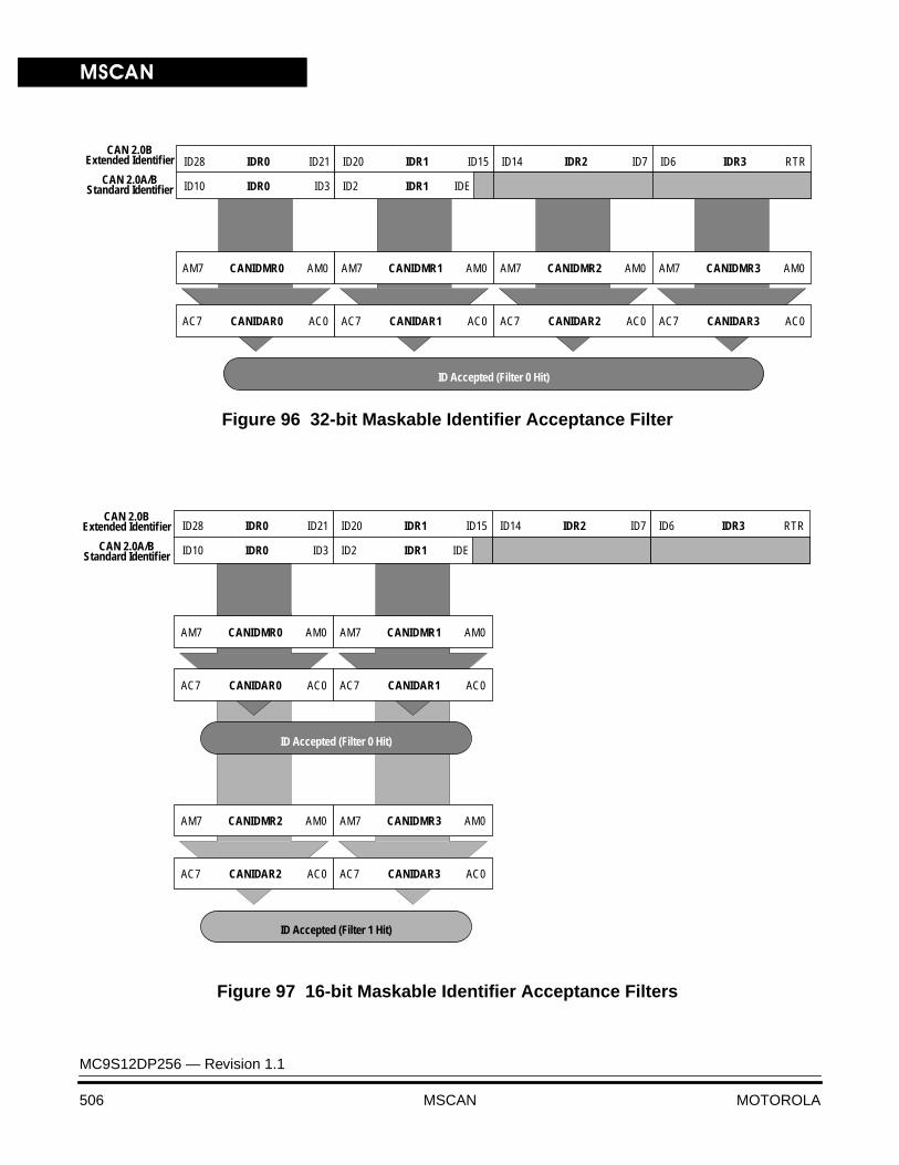
MSCAN
MC9S12DP256 — Revision 1.1
506 MSCAN MOTOROLA
Figure 96 32-bit Maskable Identifier Acceptance Filter
Figure 97 16-bit Maskable Identifier Acceptance Filters
ID28 ID21IDR0
ID10 ID3IDR0
ID20 ID15IDR1
ID2 IDEIDR1
ID14 ID7IDR2
ID10 ID3IDR2
ID6 RTRIDR3
ID10 ID3IDR3
AC7 AC0CANIDAR0
AM7 AM0CANIDMR0
AC7 AC0CANIDAR1
AM7 AM0CANIDMR1
AC7 AC0CANIDAR2
AM7 AM0CANIDMR2
AC7 AC0CANIDAR3
AM7 AM0CANIDMR3
ID Accepted (Filter 0 Hit)
CAN 2.0BExtended Identif ier
CAN 2.0A/BStandard Identif ier
ID28 ID21IDR0
ID10 ID3IDR0
ID20 ID15IDR1
ID2 IDEIDR1
ID14 ID7IDR2
ID10 ID3IDR2
ID6 RTRIDR3
ID10 ID3IDR3
AC7 AC0CANIDAR0
AM7 AM0CANIDMR0
AC7 AC0CANIDAR1
AM7 AM0CANIDMR1
ID Accepted (Filter 0 Hit)
AC7 AC0CANIDAR2
AM7 AM0CANIDMR2
AC7 AC0CANIDAR3
AM7 AM0CANIDMR3
ID Accepted (Filter 1 Hit)
CAN 2.0BExtended Identif ier
CAN 2.0A/BStandard Identif ier

MSCANFunctional Description
MC9S12DP256 — Revision 1.1
MOTOROLA MSCAN 507
Figure 98 8-bit Maskable Identifier Acceptance Filters
CAN 2.0BExtended Identif ier
CAN 2.0A/BStandard Identif ier
AC7 AC0CIDAR3
AM7 AM0CIDMR3
ID Accepted (Filter 3 Hit)
AC7 AC0CIDAR2
AM7 AM0CIDMR2
ID Accepted (Filter 2 Hit)
AC7 AC0CIDAR1
AM7 AM0CIDMR1
ID Accepted (Filter 1 Hit)
ID28 ID21IDR0
ID10 ID3IDR0
ID20 ID15IDR1
ID2 IDEIDR1
ID14 ID7IDR2
ID10 ID3IDR2
ID6 RTRIDR3
ID10 ID3IDR3
AC7 AC0CIDAR0
AM7 AM0CIDMR0
ID Accepted (Filter 0 Hit)
MSCAN
MC9S12DP256 — Revision 1.1
508 MSCAN MOTOROLA
Protocol Violation Protection
The MSCAN protects the user from accidentally violating the CAN protocol through programming errors. The protection logic implements the following features:
• The receive and transmit error counters cannot be written or otherwise manipulated.
• All registers which control the configuration of the MSCAN cannot be modified while the MSCAN is on-line. The MSCAN has to be in Initialization Mode. The corresponding INITRQ/INITAK handshake bits in the CANCTL0/CANCTL1 registers (see MSCAN Control 0 Register (CANCTL0)) serve as a lock to protect the following registers:
– MSCAN Control 1 Register (CANCTL1)
– MSCAN Bus Timing Registers 0 and 1 (CANBTR0, CANBTR1)
– MSCAN Identifier Acceptance Control Register (CANIDAC)
– MSCAN Identifier Acceptance Registers (CANIDAR0–7)
– MSCAN Identifier Mask Registers (CANIDMR0–7)
• The TxCAN pin is immediately forced to a recessive state when the MSCAN goes into the Power Down Mode or Initialization Mode (see MSCAN Power Down Mode and MSCAN Initialization Mode).
• The MSCAN enable bit (CANE) is only writable once in normal modes as further protection against inadvertently disabling the MSCAN.
Clock System Figure 99 shows the structure of the MSCAN clock generation circuitry. With this flexible clocking scheme, the MSCAN is able to handle CAN bus rates ranging from 10 Kbps up to 1 Mbps.
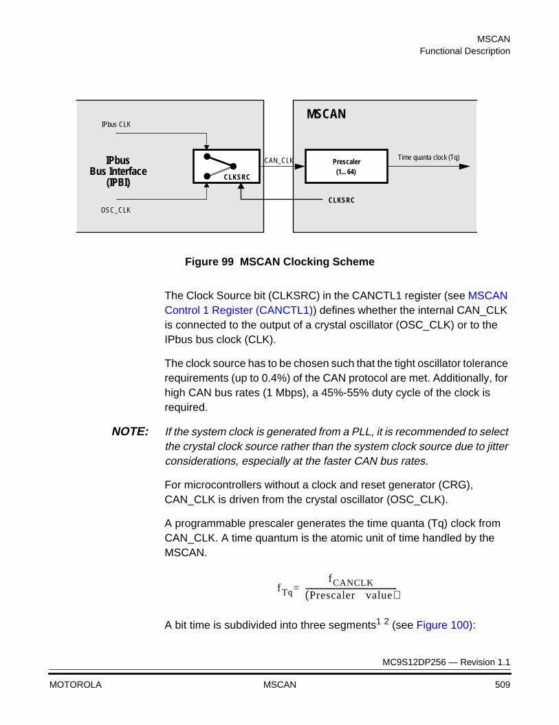
MSCANFunctional Description
MC9S12DP256 — Revision 1.1
MOTOROLA MSCAN 509
Figure 99 MSCAN Clocking Scheme
The Clock Source bit (CLKSRC) in the CANCTL1 register (see MSCAN Control 1 Register (CANCTL1)) defines whether the internal CAN_CLK is connected to the output of a crystal oscillator (OSC_CLK) or to the IPbus bus clock (CLK).
The clock source has to be chosen such that the tight oscillator tolerance requirements (up to 0.4%) of the CAN protocol are met. Additionally, for high CAN bus rates (1 Mbps), a 45%-55% duty cycle of the clock is required.
NOTE: If the system clock is generated from a PLL, it is recommended to select the crystal clock source rather than the system clock source due to jitter considerations, especially at the faster CAN bus rates.
For microcontrollers without a clock and reset generator (CRG), CAN_CLK is driven from the crystal oscillator (OSC_CLK).
A programmable prescaler generates the time quanta (Tq) clock from CAN_CLK. A time quantum is the atomic unit of time handled by the MSCAN.
A bit time is subdivided into three segments1 2 (see Figure 100):
IPbus CLK
OSC_CLK
MSCAN
IPbusBus Interface
(IPBI)
CAN_CLK
CLKSRC
CLKSRC
Prescaler(1... 64)
Time quanta clock (Tq)
fTq
fCANCLK
Prescaler value◊( )--------------------------------------------------=
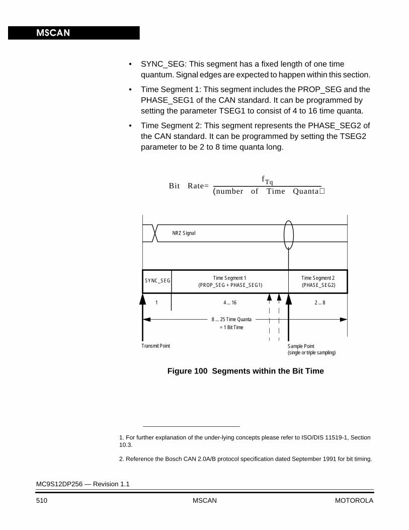
MSCAN
MC9S12DP256 — Revision 1.1
510 MSCAN MOTOROLA
• SYNC_SEG: This segment has a fixed length of one time quantum. Signal edges are expected to happen within this section.
• Time Segment 1: This segment includes the PROP_SEG and the PHASE_SEG1 of the CAN standard. It can be programmed by setting the parameter TSEG1 to consist of 4 to 16 time quanta.
• Time Segment 2: This segment represents the PHASE_SEG2 of the CAN standard. It can be programmed by setting the TSEG2 parameter to be 2 to 8 time quanta long.
Figure 100 Segments within the Bit Time
1. For further explanation of the under-lying concepts please refer to ISO/DIS 11519-1, Section 10.3.
2. Reference the Bosch CAN 2.0A/B protocol specification dated September 1991 for bit timing.
Bit RatefTq
number of Time Quanta◊ ◊ ◊( )---------------------------------------------------------------------------------=◊
SYNC_SEG Time Segment 1 Time Segment 2
1 4 ... 16 2 ... 8
8 ... 25 Time Quanta
= 1 Bit Time
NRZ Signal
Sample Point (single or triple sampling)
(PROP_SEG + PHASE_SEG1) (PHASE_SEG2)
Transmit Point

MSCANFunctional Description
MC9S12DP256 — Revision 1.1
MOTOROLA MSCAN 511
The Synchronization Jump Width1 can be programmed in a range of 1 to 4 time quanta by setting the SJW parameter.
The above parameters are set by programming the MSCAN Bus Timing Registers (CANBTR0, CANBTR1) (see MSCAN Bus Timing Register 0 (CANBTR0) and MSCAN Bus Timing Register 1 (CANBTR1)).
Figure 101 gives an overview of the CAN compliant segment settings and the related parameter values.
NOTE: It is the user’s responsibility to ensure the bit time settings are in compliance with the CAN standard.
Table 86 Time Segment Syntax
Syntax Description
SYNC_SEGSystem expects transitions to occur on the bus during this period.
Transmit PointA node in transmit mode transfers a new value to the CAN bus at this point.
Sample PointA node in receive mode samples the bus at this point. If the three samples per bit option is selected, then this point marks the position of the third sample.
1. Reference the Bosch CAN 2.0A/B protocol specification dated September 1991 for bit timing.
Time Segment 1 TSEG1 Time
Segment 2 TSEG2
Synchronization Jump Width
SJW
5 .. 10 4 .. 9 2 1 1 .. 2 0 .. 1
4 .. 11 3 .. 10 3 2 1 .. 3 0 .. 2
5 .. 12 4 .. 11 4 3 1 .. 4 0 .. 3
6 .. 13 5 .. 12 5 4 1 .. 4 0 .. 3
7 .. 14 6 .. 13 6 5 1 .. 4 0 .. 3
8 .. 15 7 .. 14 7 6 1 .. 4 0 .. 3
9 .. 16 8 .. 15 8 7 1 .. 4 0 .. 3
Figure 101 CAN Standard Compliant Bit Time Segment Settings

MSCAN
MC9S12DP256 — Revision 1.1
512 MSCAN MOTOROLA
Timer Stamp The MSCAN generates an internal time stamp whenever a valid frame is received or transmitted and the TIME bit is enabled. Because the CAN specification defines a frame to be valid if no errors occur before the End of Frame (EOF) field is transmitted successfully, the actual value of an internal timer is written at EOF to the appropriate time stamp position within the transmit buffer. For receive frames the time stamp is written to the receive buffer.
Register Descriptions
This section describes in detail all the registers and register bits in the MSCAN module.
NOTE: All bits of all registers in this module are completely synchronous to internal clocks during a register read.
ProgrammerÕs Model of Control Registers
The programmer’s model is laid out for maximum simplicity and efficiency. The Register Map provides an overview of the control registers for the MSCAN.
MSCAN Control 0 Register (CANCTL0)
The CANCTL0 register provides for various control of the MSCAN module as described below.
NOTE: The CANCTL0 register, except the WUPE, INITRQ and SLPRQ bits, is held in the reset state when the Initialization Mode is active (INITRQ=1 and INITAK=1). This register is writable again as soon as the Initialization Mode is left (INITRQ=0 and INITAK=0).
Address Offset: $0000
Bit 7 6 5 4 3 2 1 Bit 0
Read:RXFRM
RXACTCSWAI
SYNCHTIME WUPE SLPRQ INITRQ
Write:
Reset: 0 0 0 0 0 0 0 1
= Unimplemented
MSCANRegister Descriptions
MC9S12DP256 — Revision 1.1
MOTOROLA MSCAN 513
Read: anytimeWrite: anytime when out of initialization; exceptions are bits RXACT and SYNCH which are read-only and bit RXFRM which is set by the module. A write of ‘1’ to the RXFRM register clears the flag and a write of ‘0’ is ignored
RXFRM — Received Frame Flag
This bit is read and clear only. It is set when a receiver has received a valid message correctly, independently of the filter configuration. Once set, it remains set until cleared by software or reset. Clearing is done by writing a ‘1’ to the bit. This bit is not valid in loop back mode.
1 = A valid message was received since last clearing of this flag0 = No valid message was received since last clearing this flag.
NOTE: The MSCAN must be in run mode for this bit to become set.
RXACT — Receiver Active Status
This flag indicates the MSCAN is receiving a message. The flag is controlled by the receiver front end. This bit is not valid in loop back mode.
1 = MSCAN is receiving a message (including when arbitration is
lost)1
0 = MSCAN is transmitting or idle1.
CSWAI — CAN Stops in Wait Mode
Enabling this bit allows for lower power consumption in Wait Mode by disabling all the clocks at the bus interface to the MSCAN module.
1 = The module ceases to be clocked during WAIT mode.0 = The module is not affected during WAIT mode.
CAUTION: In order to protect from accidentally violating the CAN protocol the TxCAN pin is immediately forced to a recessive state when the MCU enters Wait (CSWAI=1) or Stop Mode (see MSCAN Power Down Mode)
1. See the Bosch CAN 2.0A/B protocol specification dated September 1991 for a detailed defi-nition of transmitter and receiver states.

MSCAN
MC9S12DP256 — Revision 1.1
514 MSCAN MOTOROLA
SYNCH — Synchronized Status
This flag indicates whether the MSCAN is synchronized to the CAN bus and, as such, can participate in the communication process. It is set and cleared by the MSCAN.
1 = MSCAN is synchronized to the CAN bus.0 = MSCAN is not synchronized to the CAN bus.
TIME — Timer Enable
This bit activates an internal 16-bit wide free running timer which is clocked by the bit clock. If the timer is enabled, a 16-bit time stamp will be assigned to each transmitted/received message within the active Tx/Rx buffer. As soon as a message is acknowledged on CAN, the time stamp will be written to the highest bytes ($_E, $_F) in the appropriate buffer (see Programmer’s Model of Message Storage). The internal timer is reset (all bits set to ‘0’) when Initialization Mode is active.
1 = Enable internal MSCAN timer.0 = Disable internal MSCAN timer.
WUPE — Wake-Up Enable
This configuration bit allows the MSCAN to restart when being locked in idle state during Sleep Mode and traffic on CAN is detected (see MSCAN Sleep Mode).
1 = Wake-Up enabled – The MSCAN is able to restart.0 = Wake-Up disabled – The MSCAN ignores traffic on CAN.
CAUTION: The CPU has to make sure that the wake-up option WUPE register is enabled, if the recovery mechanism from STOP or WAIT is required.
SLPRQ — Sleep Mode Request
This bit requests the MSCAN to enter Sleep Mode, which is an internal power saving mode (see MSCAN Sleep Mode). If a message transfer on CAN is ongoing when receiving this request, MSCAN will wait until end of current message before entering Sleep Mode. The module indicates entry to Sleep Mode by setting SLPAK=1 (see MSCAN Control 1 Register (CANCTL1)). Sleep Mode will be active

MSCANRegister Descriptions
MC9S12DP256 — Revision 1.1
MOTOROLA MSCAN 515
until SLPRQ is cleared by the CPU or, depending on the setting of WUPE bit, the MSCAN detects bus activity on CAN and clears the SLPRQ itself.
1 = Sleep Mode Request – The MSCAN locks in idle state.0 = Running – The MSCAN functions normally.
NOTE: The MCU cannot clear the SLPRQ bit before the MSCAN has entered Sleep Mode (SLPRQ=1 and SLPAK=1)
INITRQ — Initialization Mode Request
When this bit is set by the CPU, the MSCAN skips to Initialization Mode (see MSCAN Initialization Mode). Any ongoing transmission or reception is aborted and synchronization to the bus is lost. The module indicates entry to Initialization Mode by setting INITAK=1 (see MSCAN Control 1 Register (CANCTL1)).
The following registers enter their hard reset state and restore their
default values: CANCTL01, CANRFLG2, CANRIER3, CANTFLG, CANTIER, CANTARQ, CANTAAK, CANTBSEL.
The registers CANCTL1, CANBTR0, CANBTR1, CANIDAC, CANIDAR0–7, CANIDMR0–7 can only be written by the CPU when the MSCAN is in Initialization Mode (INITRQ=1 and INITAK=1). The values of the error counters are not affected by initialization.
When this bit is cleared by the CPU, the MSCAN restarts and then tries to synchronize to the CAN bus. If the MSCAN is not in bus-off state, it synchronizes after 11 consecutive recessive bits on the bus; if the MSCAN is in bus-off state it continues to wait for 128 occurrences of 11 consecutive recessive bits.
Writing to other bits in CANCTL0, CANRFLG, CANRIER, CANTFLG or CANTIER must only be done after Initialization Mode is left, which is INITRQ=0 and INITAK=0.
1 = MSCAN in initialization state.0 = Normal operation.
1. except the INITRQ and SLPRQ bits
2. The TSTAT1, TSTAT0 bits are not affected by Initialization Mode
3. The RSTAT1, RSTAT0 bits are not affected by Initialization Mode
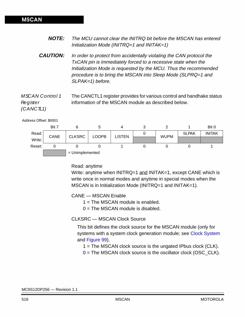
MSCAN
MC9S12DP256 — Revision 1.1
516 MSCAN MOTOROLA
NOTE: The MCU cannot clear the INITRQ bit before the MSCAN has entered Initialization Mode (INITRQ=1 and INITAK=1)
CAUTION: In order to protect from accidentally violating the CAN protocol the TxCAN pin is immediately forced to a recessive state when the Initialization Mode is requested by the MCU. Thus the recommended procedure is to bring the MSCAN into Sleep Mode (SLPRQ=1 and SLPAK=1) before.
MSCAN Control 1 Register (CANCTL1)
The CANCTL1 register provides for various control and handhake status information of the MSCAN module as described below.
Read: anytimeWrite: anytime when INITRQ=1 and INITAK=1, except CANE which is write once in normal modes and anytime in special modes when the MSCAN is in Initialization Mode (INITRQ=1 and INITAK=1).
CANE — MSCAN Enable1 = The MSCAN module is enabled.0 = The MSCAN module is disabled.
CLKSRC — MSCAN Clock Source
This bit defines the clock source for the MSCAN module (only for systems with a system clock generation module; see Clock System and Figure 99).
1 = The MSCAN clock source is the ungated IPbus clock (CLK).0 = The MSCAN clock source is the oscillator clock (OSC_CLK).
Address Offset: $0001
Bit 7 6 5 4 3 2 1 Bit 0
Read:CANE CLKSRC LOOPB LISTEN
0WUPM
SLPAK INITAK
Write:
Reset: 0 0 0 1 0 0 0 1
= Unimplemented
MSCANRegister Descriptions
MC9S12DP256 — Revision 1.1
MOTOROLA MSCAN 517
LOOPB — Loop Back Self Test Mode
When this bit is set, the MSCAN performs an internal loop back which can be used for self test operation. The bit stream output of the transmitter is fed back to the receiver internally. The RxCAN input pin is ignored and the TxCAN output goes to the recessive state (logic ‘1’). The MSCAN behaves as it does normally when transmitting and treats its own transmitted message as a message received from a remote node. In this state, the MSCAN ignores the bit sent during the ACK slot in the CAN frame Acknowledge field to ensure proper reception of its own message. Both transmit and receive interrupts are generated.
LISTEN — Listen Only Mode
This bit configures the MSCAN as a bus monitor. When the bit is set, all valid CAN messages with matching ID are received, but no acknowledgement or error frames are sent out (see Listen-Only Mode). In addition the error counters are frozen. Listen Only Mode supports applications which require ‘hot plugging’ or throughput analysis. The MSCAN is unable to transmit any messages, when Listen Only Mode is active.
1 = Listen Only Mode activated0 = normal operation
WUPM — Wake-Up Mode
This bit defines whether the integrated low-pass filter is applied to protect the MSCAN from spurious wake-up (see MSCAN Sleep Mode).
1 = MSCAN wakes-up the CPU only in case of a dominant pulse on the bus which has a length of Twup and WUPE=1 in
CANCTL0 (see MSCAN Control 0 Register (CANCTL0)).0 = MSCAN wakes-up the CPU after any recessive to dominant
edge on the CAN bus and WUPE=1 in CANCTL0.
SLPAK — Sleep Mode Acknowledge
This flag indicates whether the MSCAN module has entered Sleep Mode (see MSCAN Sleep Mode). It is used as a handshake flag for the SLPRQ Sleep Mode request. Sleep Mode is active when
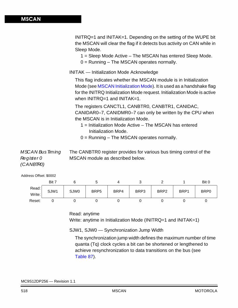
MSCAN
MC9S12DP256 — Revision 1.1
518 MSCAN MOTOROLA
INITRQ=1 and INITAK=1. Depending on the setting of the WUPE bit the MSCAN will clear the flag if it detects bus activity on CAN while in Sleep Mode.
1 = Sleep Mode Active – The MSCAN has entered Sleep Mode.0 = Running – The MSCAN operates normally.
INITAK — Initialization Mode Acknowledge
This flag indicates whether the MSCAN module is in Initialization Mode (see MSCAN Initialization Mode). It is used as a handshake flag for the INITRQ Initialization Mode request. Initialization Mode is active when INITRQ=1 and INITAK=1.
The registers CANCTL1, CANBTR0, CANBTR1, CANIDAC, CANIDAR0–7, CANIDMR0–7 can only be written by the CPU when the MSCAN is in Initialization Mode.
1 = Initialization Mode Active – The MSCAN has entered Initialization Mode.
0 = Running – The MSCAN operates normally.
MSCAN Bus Timing Register 0 (CANBTR0)
The CANBTR0 register provides for various bus timing control of the MSCAN module as described below.
Read: anytimeWrite: anytime in Initialization Mode (INITRQ=1 and INITAK=1)
SJW1, SJW0 — Synchronization Jump Width
The synchronization jump width defines the maximum number of time quanta (Tq) clock cycles a bit can be shortened or lengthened to achieve resynchronization to data transitions on the bus (see Table 87).
Address Offset: $0002
Bit 7 6 5 4 3 2 1 Bit 0
Read:SJW1 SJW0 BRP5 BRP4 BRP3 BRP2 BRP1 BRP0
Write:
Reset: 0 0 0 0 0 0 0 0
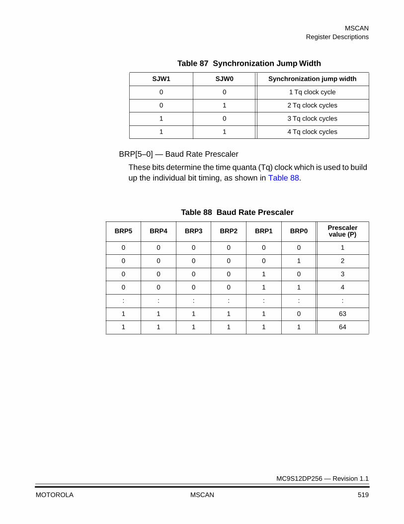
MSCANRegister Descriptions
MC9S12DP256 — Revision 1.1
MOTOROLA MSCAN 519
BRP[5–0] — Baud Rate Prescaler
These bits determine the time quanta (Tq) clock which is used to build up the individual bit timing, as shown in Table 88.
Table 87 Synchronization Jump Width
SJW1 SJW0 Synchronization jump width
0 0 1 Tq clock cycle
0 1 2 Tq clock cycles
1 0 3 Tq clock cycles
1 1 4 Tq clock cycles
Table 88 Baud Rate Prescaler
BRP5 BRP4 BRP3 BRP2 BRP1 BRP0 Prescaler value (P)
0 0 0 0 0 0 1
0 0 0 0 0 1 2
0 0 0 0 1 0 3
0 0 0 0 1 1 4
: : : : : : :
1 1 1 1 1 0 63
1 1 1 1 1 1 64
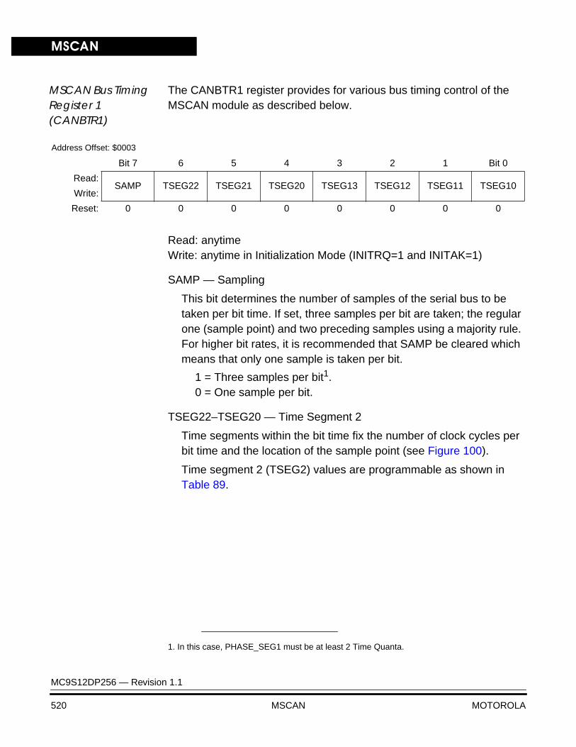
MSCAN
MC9S12DP256 — Revision 1.1
520 MSCAN MOTOROLA
MSCAN Bus Timing Register 1 (CANBTR1)
The CANBTR1 register provides for various bus timing control of the MSCAN module as described below.
Read: anytimeWrite: anytime in Initialization Mode (INITRQ=1 and INITAK=1)
SAMP — Sampling
This bit determines the number of samples of the serial bus to be taken per bit time. If set, three samples per bit are taken; the regular one (sample point) and two preceding samples using a majority rule. For higher bit rates, it is recommended that SAMP be cleared which means that only one sample is taken per bit.
1 = Three samples per bit1.0 = One sample per bit.
TSEG22–TSEG20 — Time Segment 2
Time segments within the bit time fix the number of clock cycles per bit time and the location of the sample point (see Figure 100).
Time segment 2 (TSEG2) values are programmable as shown in Table 89.
Address Offset: $0003
Bit 7 6 5 4 3 2 1 Bit 0
Read:SAMP TSEG22 TSEG21 TSEG20 TSEG13 TSEG12 TSEG11 TSEG10
Write:
Reset: 0 0 0 0 0 0 0 0
1. In this case, PHASE_SEG1 must be at least 2 Time Quanta.
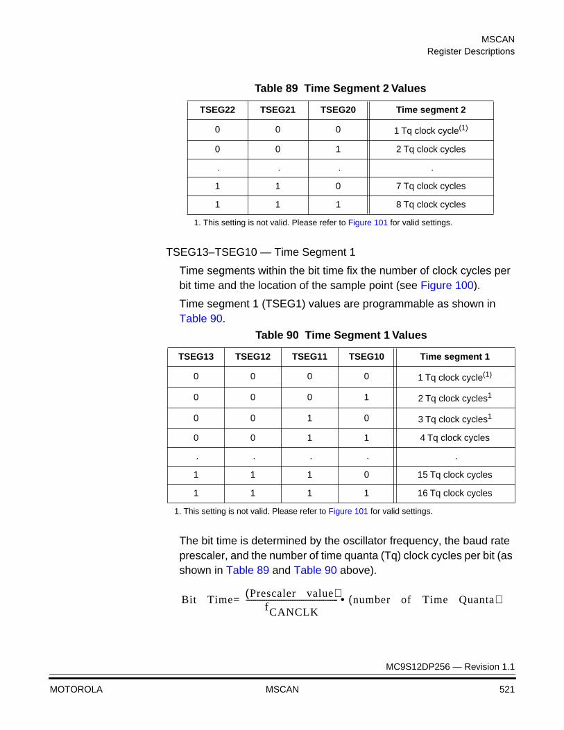
MSCANRegister Descriptions
MC9S12DP256 — Revision 1.1
MOTOROLA MSCAN 521
TSEG13–TSEG10 — Time Segment 1
Time segments within the bit time fix the number of clock cycles per bit time and the location of the sample point (see Figure 100).
Time segment 1 (TSEG1) values are programmable as shown in Table 90.
The bit time is determined by the oscillator frequency, the baud rate prescaler, and the number of time quanta (Tq) clock cycles per bit (as shown in Table 89 and Table 90 above).
Table 89 Time Segment 2 Values
TSEG22 TSEG21 TSEG20 Time segment 2
0 0 0 1 Tq clock cycle(1)
1. This setting is not valid. Please refer to Figure 101 for valid settings.
0 0 1 2 Tq clock cycles
. . . .
1 1 0 7 Tq clock cycles
1 1 1 8 Tq clock cycles
Table 90 Time Segment 1 Values
TSEG13 TSEG12 TSEG11 TSEG10 Time segment 1
0 0 0 0 1 Tq clock cycle(1)
1. This setting is not valid. Please refer to Figure 101 for valid settings.
0 0 0 1 2 Tq clock cycles1
0 0 1 0 3 Tq clock cycles1
0 0 1 1 4 Tq clock cycles
. . . . .
1 1 1 0 15 Tq clock cycles
1 1 1 1 16 Tq clock cycles
Bit TimePrescaler value◊( )
fCANCLK-------------------------------------------------- number of Time Quanta◊ ◊ ◊( )•=◊
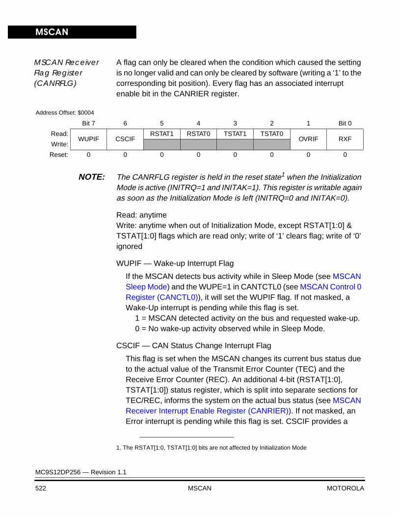
MSCAN
MC9S12DP256 — Revision 1.1
522 MSCAN MOTOROLA
MSCAN Receiver Flag Register (CANRFLG)
A flag can only be cleared when the condition which caused the setting is no longer valid and can only be cleared by software (writing a ‘1’ to the corresponding bit position). Every flag has an associated interrupt enable bit in the CANRIER register.
NOTE: The CANRFLG register is held in the reset state1 when the Initialization Mode is active (INITRQ=1 and INITAK=1). This register is writable again as soon as the Initialization Mode is left (INITRQ=0 and INITAK=0).
Read: anytimeWrite: anytime when out of Initialization Mode, except RSTAT[1:0] & TSTAT[1:0] flags which are read only; write of ‘1’ clears flag; write of ‘0’ ignored
WUPIF — Wake-up Interrupt Flag
If the MSCAN detects bus activity while in Sleep Mode (see MSCAN Sleep Mode) and the WUPE=1 in CANTCTL0 (see MSCAN Control 0 Register (CANCTL0)), it will set the WUPIF flag. If not masked, a Wake-Up interrupt is pending while this flag is set.
1 = MSCAN detected activity on the bus and requested wake-up.0 = No wake-up activity observed while in Sleep Mode.
CSCIF — CAN Status Change Interrupt Flag
This flag is set when the MSCAN changes its current bus status due to the actual value of the Transmit Error Counter (TEC) and the Receive Error Counter (REC). An additional 4-bit (RSTAT[1:0], TSTAT[1:0]) status register, which is split into separate sections for TEC/REC, informs the system on the actual bus status (see MSCAN Receiver Interrupt Enable Register (CANRIER)). If not masked, an Error interrupt is pending while this flag is set. CSCIF provides a
Address Offset: $0004
Bit 7 6 5 4 3 2 1 Bit 0
Read:WUPIF CSCIF
RSTAT1 RSTAT0 TSTAT1 TSTAT0OVRIF RXF
Write:
Reset: 0 0 0 0 0 0 0 0
1. The RSTAT[1:0, TSTAT[1:0] bits are not affected by Initialization Mode
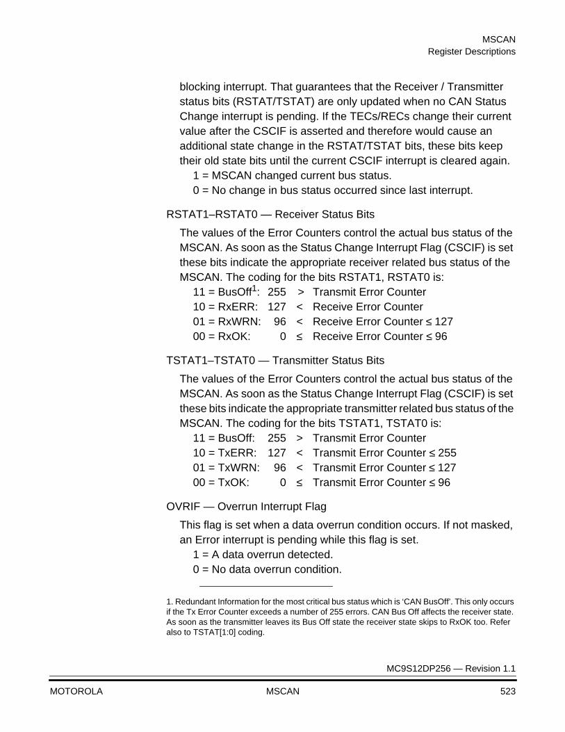
MSCANRegister Descriptions
MC9S12DP256 — Revision 1.1
MOTOROLA MSCAN 523
blocking interrupt. That guarantees that the Receiver / Transmitter status bits (RSTAT/TSTAT) are only updated when no CAN Status Change interrupt is pending. If the TECs/RECs change their current value after the CSCIF is asserted and therefore would cause an additional state change in the RSTAT/TSTAT bits, these bits keep their old state bits until the current CSCIF interrupt is cleared again.
1 = MSCAN changed current bus status.0 = No change in bus status occurred since last interrupt.
RSTAT1–RSTAT0 — Receiver Status Bits
The values of the Error Counters control the actual bus status of the MSCAN. As soon as the Status Change Interrupt Flag (CSCIF) is set these bits indicate the appropriate receiver related bus status of the MSCAN. The coding for the bits RSTAT1, RSTAT0 is:
11 = BusOff1: 255 > Transmit Error Counter10 = RxERR: 127 < Receive Error Counter01 = RxWRN: 96 < Receive Error Counter ≤ 127 00 = RxOK: 0 ≤ Receive Error Counter ≤ 96
TSTAT1–TSTAT0 — Transmitter Status Bits
The values of the Error Counters control the actual bus status of the MSCAN. As soon as the Status Change Interrupt Flag (CSCIF) is set these bits indicate the appropriate transmitter related bus status of the MSCAN. The coding for the bits TSTAT1, TSTAT0 is:
11 = BusOff: 255 > Transmit Error Counter10 = TxERR: 127 < Transmit Error Counter ≤ 255 01 = TxWRN: 96 < Transmit Error Counter ≤ 127 00 = TxOK: 0 ≤ Transmit Error Counter ≤ 96
OVRIF — Overrun Interrupt Flag
This flag is set when a data overrun condition occurs. If not masked, an Error interrupt is pending while this flag is set.
1 = A data overrun detected.0 = No data overrun condition.
1. Redundant Information for the most critical bus status which is ‘CAN BusOff’. This only occurs if the Tx Error Counter exceeds a number of 255 errors. CAN Bus Off affects the receiver state. As soon as the transmitter leaves its Bus Off state the receiver state skips to RxOK too. Refer also to TSTAT[1:0] coding.

MSCAN
MC9S12DP256 — Revision 1.1
524 MSCAN MOTOROLA
RXF — Receive Buffer Full
The RXF flag is set by the MSCAN when a new message is available in the receiver FIFO. This flag indicates whether the shifted buffer is loaded with a correctly received message (matching identifier, matching Cyclic Redundancy Code (CRC) and no other errors detected). After the CPU has read that message from the RxFG buffer in the receiver FIFO, the RXF flag must be cleared to release the buffer. Depending on the clocking relationship between CAN and CPU clock domain the time until the RXF flag gets asserted again will
vary1. A set RXF flag prohibits the shifting of the next FIFO entry into the foreground buffer (RxFG). If not masked, a Receive interrupt is pending while this flag is set.
1 = The receiver FIFO is not empty. A new message is available in the RxFG.
0 = No new message available within the RxFG.
WARNING: To ensure data integrity, do not read the receive buffer registers while the RXF flag is cleared.
MSCAN Receiver Interrupt Enable Register (CANRIER)
This register contains the interrupt enable bits for the interrupt flags described above.
NOTE: The CANRIER register is held in the reset state2 when the Initialization Mode is active (INITRQ=1 and INITAK=1). This register is writable again as soon as the Initialization Mode is left (INITRQ=0 and INITAK=0).
1. In case there is another CAN message in the FIFO buffer.
Address Offset: $0005
Bit 7 6 5 4 3 2 1 Bit 0
Read:WUPIE CSCIE RSTATE1 RSTATE0 TSTATE1 TSTATE0 OVRIE RXFIE
Write:
Reset: 0 0 0 0 0 0 0 0
2. The RSTATE[1:0], TSTATE[1:0] bits are not affected by Initialization Mode
MSCANRegister Descriptions
MC9S12DP256 — Revision 1.1
MOTOROLA MSCAN 525
Read: anytimeWrite: anytime when out of Initialization Mode
WUPIE — Wake-up Interrupt Enable1 = A wake-up event causes a wake-up interrupt request.0 = No interrupt request is generated from this event.
NOTE: The CPU has to make sure that the Wake-up interrupt register and the WUPE register (see MSCAN Control 0 Register (CANCTL0)) is enabled, if the recovery mechanism from STOP or WAIT is required.
CSCIE — CAN Status Change Interrupt Enable1 = A CAN Status Change event causes an error interrupt request.0 = No interrupt request is generated from this event.
RSTATE1, RSTATE0— Receiver Status Change Enable
These RSTAT enable bits control the sensitivity level in which receiver state changes are causing CSCIF interrupts. Independent of the chosen sensitivity level the RSTAT flags still indicate the actual receiver state and are only updated if no CSCIF interrupt is pending.
11 = generate CSCIF interrupt on all state changes 10 = generate CSCIF interrupt only if the receiver enters or leaves
‘RxErr’ or ‘BusOff’1 state. Discard other receiver state changes for generating CSCIF interrupt.
01 = generate CSCIF interrupt only if the receiver enters or leaves ‘BusOff’ state. Discard other receiver state changes for generating CSCIF interrupt.
00 = do not generate any CSCIF interrupt caused by receiver state changes.
1. BusOff state is only defined by the CAN standard for transmitters. Because the only possible state change for the transmitter from BusOff to TxOK also forces the receiver to skip its current state to RxOK, the coding of the RXSTAT[1:0] flags define an additional BusOff state for the re-ceiver (see MSCAN Receiver Flag Register (CANRFLG))
MSCAN
MC9S12DP256 — Revision 1.1
526 MSCAN MOTOROLA
TSTATE1, TSTATE0 — Transmitter Status Change Enable
These TSTAT enable bits control the sensitivity level in which transmitter state changes are causing CSCIF interrupts. Independent of the chosen sensitivity level the TSTAT flags still indicate the actual transmitter state and are only updated if no CSCIF interrupt is pending.
11 = generate CSCIF interrupt on all state changes10 = generate CSCIF interrupt only if the transmitter enters or
leaves ‘TxErr’ or ‘BusOff’ state. Discard other transmitter state changes for generating CSCIF interrupt.
01 = generate CSCIF interrupt only if the transmitter enters or leaves ‘BusOff’ state. Discard other transmitter state changes for generating CSCIF interrupt.
00 = do not generate any CSCIF interrupt caused by transmitter state changes.
OVRIE — Overrun Interrupt Enable1 = An overrun event causes an error interrupt request.0 = No interrupt request is generated from this event.
RXFIE — Receiver Full Interrupt Enable1 = A receive buffer full (successful message reception) event
causes a receiver interrupt request.0 = No interrupt request is generated from this event.
MSCAN Transmitter Flag Register (CANTFLG)
The Transmit Buffer Empty flags each have an associated interrupt enable bit in the CANTIER register.
Address Offset: $0006
Bit 7 6 5 4 3 2 1 Bit 0
Read: 0 0 0 0 0TXE2 TXE1 TXE0
Write:
Reset: 0 0 0 0 0 1 1 1
= Unimplemented

MSCANRegister Descriptions
MC9S12DP256 — Revision 1.1
MOTOROLA MSCAN 527
NOTE: The CANTFLG register is held in the reset state when the Initialization Mode is active (INITRQ=1 and INITAK=1). This register is writable again as soon as the Initialization Mode is left (INITRQ=0 and INITAK=0).
Read: anytimeWrite: anytime for TXEx flags when not in Initialization Mode; write of ‘1’ clears flag, write of ‘0’ ignored
TXE2–TXE0 —Transmitter Buffer Empty
This flag indicates that the associated transmit message buffer is empty, and thus not scheduled for transmission. The CPU must clear the flag after a message is set up in the transmit buffer and is due for transmission. The MSCAN sets the flag after the message is sent successfully. The flag is also set by the MSCAN when the transmission request is successfully aborted due to a pending abort request (see MSCAN Transmitter Message Abort Control (CANTARQ)). If not masked, a Transmit interrupt is pending while this flag is set.
Clearing a TXEx flag also clears the corresponding ABTAKx (see MSCAN Transmitter Message Abort Control (CANTAAK)). When a TXEx flag is set, the corresponding ABTRQx bit is cleared (see MSCAN Transmitter Message Abort Control (CANTARQ)).
When Listen-Mode is active (see MSCAN Control 1 Register (CANCTL1)) the TXEx flags cannot be cleared and no transmission is started.
1 = The associated message buffer is empty (not scheduled).0 = The associated message buffer is full (loaded with a message
due for transmission).
WARNING: To ensure data integrity, do not write to the transmit buffer registers while the associated TXE flag is cleared.
MSCAN
MC9S12DP256 — Revision 1.1
528 MSCAN MOTOROLA
MSCAN Transmitter Interrupt Enable Register (CANTIER)
This register contains the interrupt enable bits for the Transmit Buffer Empty interrupt flags.
NOTE: The CANTCR register is held in the reset state when the Initialization Mode is active (INITRQ=1 and INITAK=1). This register is writable again as soon as the Initialization Mode is left (INITRQ=0 and INITAK=0).
Read: anytimeWrite: anytime when not in Initialization Mode
TXEIE2–TXEIE0 — Transmitter Empty Interrupt Enable1 = A transmitter empty (transmit buffer available for transmission)
event causes a transmitter empty interrupt request.0 = No interrupt request is generated from this event.
Address Offset: $0007
Bit 7 6 5 4 3 2 1 Bit 0
Read: 0 0 0 0 0TXEIE2 TXEIE1 TXEIE0
Write:
Reset: 0 0 0 0 0 0 0 0
= Unimplemented

MSCANRegister Descriptions
MC9S12DP256 — Revision 1.1
MOTOROLA MSCAN 529
MSCAN Transmitter Message Abort Control (CANTARQ)
The CANTARQ register provides for abort request of queued messages as described below.
NOTE: The CANTARQ register is held in the reset state when the Initialization Mode is active (INITRQ=1 and INITAK=1). This register is writable again as soon as the Initialization Mode is left (INITRQ=0 and INITAK=0).
Read: anytimeWrite: anytime when not in Initialization Mode
ABTRQ2–ABTRQ0 — Abort Request
The CPU sets the ABTRQx bit to request that a scheduled message buffer (TXEx=0) be aborted. The MSCAN grants the request if the message has not already started transmission, or if the transmission is not successful (lost arbitration or error). When a message is aborted, the associated TXE (see MSCAN Transmitter Flag Register (CANTFLG)) and Abort Acknowledge flags (ABTAK, see MSCAN Transmitter Message Abort Control (CANTAAK)) are set and a transmit interrupt occurs if enabled. The CPU cannot reset ABTRQx. ABTRQx is reset whenever the associated TXE flag is set.
1 = Abort request pending.0 = No abort request.
Address Offset: $0008
Bit 7 6 5 4 3 2 1 Bit 0
Read: 0 0 0 0 0ABTRQ2 ABTRQ1 ABTRQ0
Write:
Reset: 0 0 0 0 0 0 0 0
= Unimplemented

MSCAN
MC9S12DP256 — Revision 1.1
530 MSCAN MOTOROLA
MSCAN Transmitter Message Abort Control (CANTAAK)
The CANTAAK register indicates the successful abort of a queued message, if requested by the appropriate bits in the CANTARQ register
NOTE: The CANTAAK register is held in the reset state when the Initialization Mode is active (INITRQ=1 and INITAK=1).
Read: anytimeWrite: unimplemented for ABTAKx flags;
ABTAK2–ABTAK0 — Abort Acknowledge
This flag acknowledges that a message was aborted due to a pending abort request from the CPU. After a particular message buffer is flagged empty, this flag can be used by the application software to identify whether the message was aborted successfully or was sent anyway. The ABTAKx flag is cleared whenever the corresponding TXE flag is cleared.
1 = The message was aborted.0 = The message was not aborted.
Address Offset: $0009
Bit 7 6 5 4 3 2 1 Bit 0
Read: 0 0 0 0 0 ABTAK2 ABTAK1 ABTAK0
Write:
Reset: 0 0 0 0 0 0 0 0
= Unimplemented

MSCANRegister Descriptions
MC9S12DP256 — Revision 1.1
MOTOROLA MSCAN 531
MSCAN Transmit Buffer Selection (CANTBSEL)
The CANTBSEL register allows the selection of the actual transmit message buffer, which will be then accessible in the CANTXFG register space (see Programmer’s Model of Control Registers).
NOTE: The CANTBSEL register is held in the reset state when the Initialization Mode is active (INITRQ=1 and INITAK=1). This register is writable again as soon as the Initialization Mode is left (INITRQ=0 and INITAK=0).
Read: find the lowest ordered bit set to ‘1’, all other bits will be read as ‘0’ Write: anytime when not in Initialization Mode
Tx2–TX0 — Transmit Buffer Select
The lowest numbered bit places the respective transmit buffer in the CANTXFG register space (e.g. TX1=1 and TX0=1 selects transmit buffer TX0, TX1=1 and TX0=0 selects transmit buffer TX1)
1 = The associated message Buffer is selected, if lowest numbered bit.
0 = The associated message buffer is deselected
NOTE: The following gives a short programming example of the usage of the CANTBSEL register:
The application software wants to get the next available transmit buffer. It reads the CANTFLG register and writes this value back into the CANTBSEL register. In this example Tx buffers TX1 and TX2 are available. The value read from CANTFLG is therefore 8’b0000_0110. When writing this value back to CANTBSEL the Tx buffer TX1 is selected in the CANTXFG because the lowest numbered bit set to ‘1’ is at bit position 1. Reading back this value out of CANTBSEL results in 8’b0000_0010, because only the lowest numbered bit position set to ‘1’ is prsented. This mechanism eases the application software the selection of the next available Tx buffer.
Address Offset: $000A
Bit 7 6 5 4 3 2 1 Bit 0
Read: 0 0 0 0 0TX2 TX1 TX0
Write:
Reset: 0 0 0 0 0 0 0 0
= Unimplemented

MSCAN
MC9S12DP256 — Revision 1.1
532 MSCAN MOTOROLA
LDAA CANTFLG ; value read is 8’b0000_0110STAA CANTBSEL ; value written is 8’b0000_0110LDAA CANTBSEL ; value read is 8’b0000_0010
. ;
. ; Fill TxBuffer
. ;LDAA CANTBSEL ; Read actual TxBuffer selectionSTAA CANTFLG ; Transmit selected TxBuffer
NOTE: If all transmit message buffers are deselected no accesses are allowed to the CANTXFG registers.
MSCAN Identifier Acceptance Control Register (CANIDAC)
The CANIDAC register provides for identifier acceptance control as described below.
Read: anytimeWrite: anytime in Initialization Mode (INITRQ=1 and INITAK=1), except bits IDHITx which are unimplemented
IDAM1–IDAM0 — Identifier Acceptance Mode
The CPU sets these flags to define the identifier acceptance filter organization (see Identifier Acceptance Filter). Table 91 summarizes the different settings. In Filter Closed mode, no message is accepted such that the foreground buffer is never reloaded.
Address Offset: $000B
Bit 7 6 5 4 3 2 1 Bit 0
Read: 0 0IDAM1 IDAM0
0 IDHIT2 IDHIT1 IDHIT0
Write:
Reset: 0 0 0 0 0 0 0 0
= Unimplemented
MSCANRegister Descriptions
MC9S12DP256 — Revision 1.1
MOTOROLA MSCAN 533
IDHIT2–IDHIT0 — Identifier Acceptance Hit Indicator
The MSCAN sets these flags to indicate an identifier acceptance hit (see Identifier Acceptance Filter). Table 92 summarizes the different settings.
The IDHITx indicators are always related to the message in the foreground buffer (RxFG). When a message gets shifted into the foreground buffer of the receiver FIFO the indicators are updated as well.
Reserved Registers These registers are reserved for factory testing of the MSCAN module and are not available in normal modes.
Table 91 Identifier Acceptance Mode Settings
IDAM1 IDAM0 Identifier Acceptance Mode
0 0 Two 32 bit Acceptance Filters
0 1 Four 16 bit Acceptance Filters
1 0 Eight 8 bit Acceptance Filters
1 1 Filter Closed
Table 92 Identifier Acceptance Hit Indication
IDHIT2 IDHIT1 IDHIT0 Identifier Acceptance Hit
0 0 0 Filter 0 Hit
0 0 1 Filter 1 Hit
0 1 0 Filter 2 Hit
0 1 1 Filter 3 Hit
1 0 0 Filter 4 Hit
1 0 1 Filter 5 Hit
1 1 0 Filter 6 Hit
1 1 1 Filter 7 Hit
Address Offset: $000C–$000D
Bit 7 6 5 4 3 2 1 Bit 0
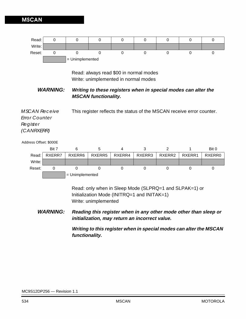
MSCAN
MC9S12DP256 — Revision 1.1
534 MSCAN MOTOROLA
Read: always read $00 in normal modesWrite: unimplemented in normal modes
WARNING: Writing to these registers when in special modes can alter the MSCAN functionality.
MSCAN Receive Error Counter Register (CANRXERR)
This register reflects the status of the MSCAN receive error counter.
Read: only when in Sleep Mode (SLPRQ=1 and SLPAK=1) or Initialization Mode (INITRQ=1 and INITAK=1)Write: unimplemented
WARNING: Reading this register when in any other mode other than sleep or initialization, may return an incorrect value.
Writing to this register when in special modes can alter the MSCAN functionality.
Read: 0 0 0 0 0 0 0 0
Write:
Reset: 0 0 0 0 0 0 0 0
= Unimplemented
Address Offset: $000E
Bit 7 6 5 4 3 2 1 Bit 0
Read: RXERR7 RXERR6 RXERR5 RXERR4 RXERR3 RXERR2 RXERR1 RXERR0
Write:
Reset: 0 0 0 0 0 0 0 0
= Unimplemented
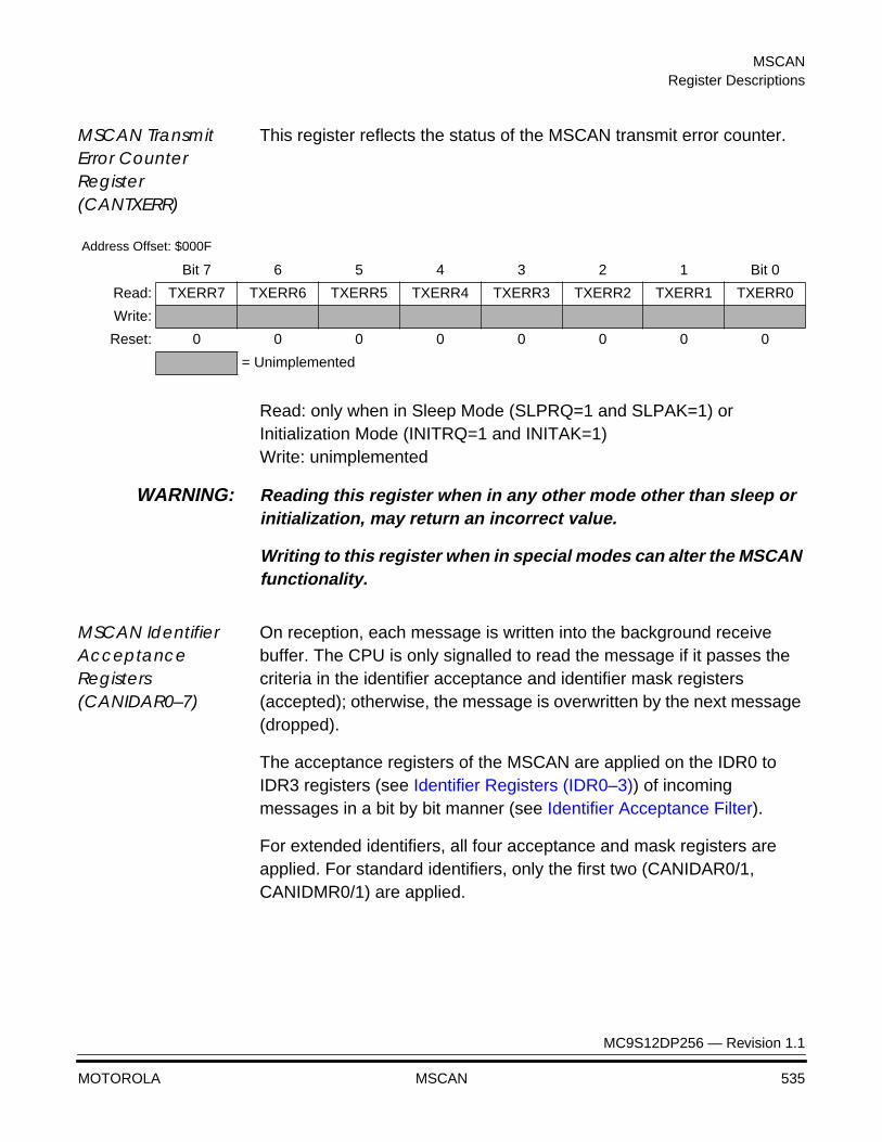
MSCANRegister Descriptions
MC9S12DP256 — Revision 1.1
MOTOROLA MSCAN 535
MSCAN Transmit Error Counter Register (CANTXERR)
This register reflects the status of the MSCAN transmit error counter.
Read: only when in Sleep Mode (SLPRQ=1 and SLPAK=1) or Initialization Mode (INITRQ=1 and INITAK=1) Write: unimplemented
WARNING: Reading this register when in any other mode other than sleep or initialization, may return an incorrect value.
Writing to this register when in special modes can alter the MSCAN functionality.
MSCAN Identifier Acceptance Registers (CANIDAR0–7)
On reception, each message is written into the background receive buffer. The CPU is only signalled to read the message if it passes the criteria in the identifier acceptance and identifier mask registers (accepted); otherwise, the message is overwritten by the next message (dropped).
The acceptance registers of the MSCAN are applied on the IDR0 to IDR3 registers (see Identifier Registers (IDR0–3)) of incoming messages in a bit by bit manner (see Identifier Acceptance Filter).
For extended identifiers, all four acceptance and mask registers are applied. For standard identifiers, only the first two (CANIDAR0/1, CANIDMR0/1) are applied.
Address Offset: $000F
Bit 7 6 5 4 3 2 1 Bit 0
Read: TXERR7 TXERR6 TXERR5 TXERR4 TXERR3 TXERR2 TXERR1 TXERR0
Write:
Reset: 0 0 0 0 0 0 0 0
= Unimplemented
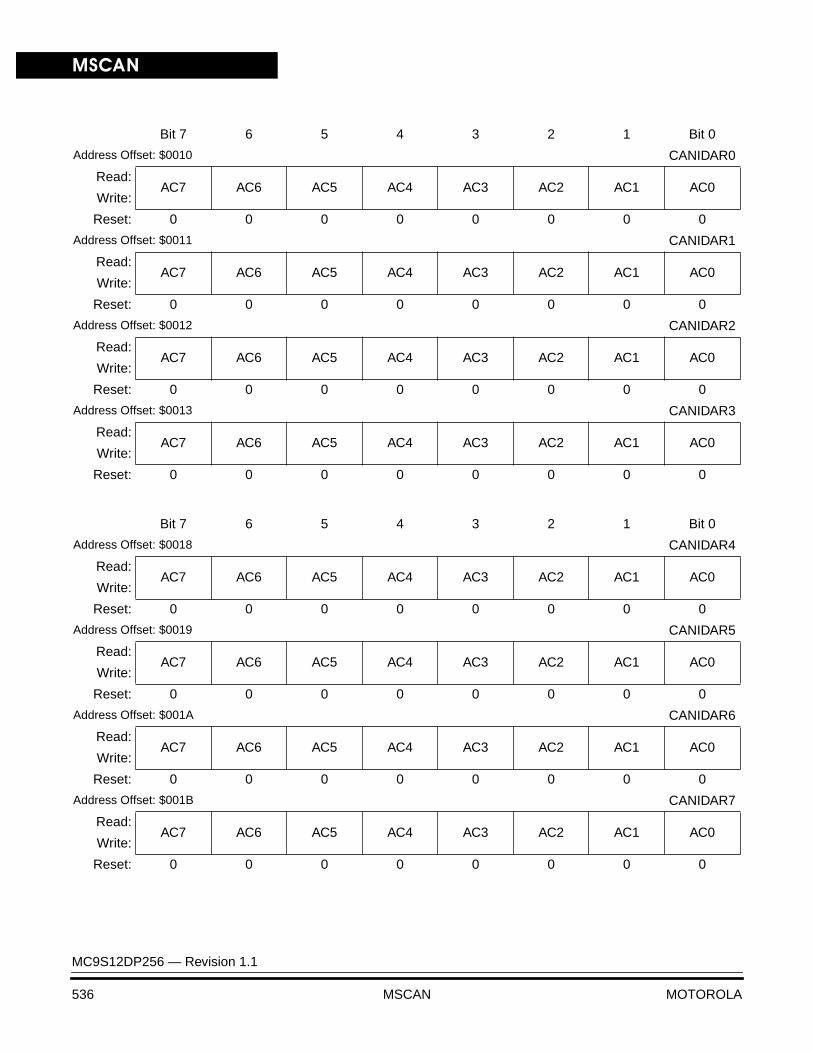
MSCAN
MC9S12DP256 — Revision 1.1
536 MSCAN MOTOROLA
Bit 7 6 5 4 3 2 1 Bit 0
Address Offset: $0010 CANIDAR0
Read:AC7 AC6 AC5 AC4 AC3 AC2 AC1 AC0
Write:
Reset: 0 0 0 0 0 0 0 0
Address Offset: $0011 CANIDAR1
Read:AC7 AC6 AC5 AC4 AC3 AC2 AC1 AC0
Write:
Reset: 0 0 0 0 0 0 0 0
Address Offset: $0012 CANIDAR2
Read:AC7 AC6 AC5 AC4 AC3 AC2 AC1 AC0
Write:
Reset: 0 0 0 0 0 0 0 0
Address Offset: $0013 CANIDAR3
Read:AC7 AC6 AC5 AC4 AC3 AC2 AC1 AC0
Write:
Reset: 0 0 0 0 0 0 0 0
Bit 7 6 5 4 3 2 1 Bit 0
Address Offset: $0018 CANIDAR4
Read:AC7 AC6 AC5 AC4 AC3 AC2 AC1 AC0
Write:
Reset: 0 0 0 0 0 0 0 0
Address Offset: $0019 CANIDAR5
Read:AC7 AC6 AC5 AC4 AC3 AC2 AC1 AC0
Write:
Reset: 0 0 0 0 0 0 0 0
Address Offset: $001A CANIDAR6
Read:AC7 AC6 AC5 AC4 AC3 AC2 AC1 AC0
Write:
Reset: 0 0 0 0 0 0 0 0
Address Offset: $001B CANIDAR7
Read:AC7 AC6 AC5 AC4 AC3 AC2 AC1 AC0
Write:
Reset: 0 0 0 0 0 0 0 0

MSCANRegister Descriptions
MC9S12DP256 — Revision 1.1
MOTOROLA MSCAN 537
Read: anytimeWrite: anytime in Initialization Mode (INITRQ=1 and INITAK=1)
AC7–AC0 — Acceptance Code Bits
AC7–AC0 comprise a user defined sequence of bits with which the corresponding bits of the related identifier register (IDRn) of the receive message buffer are compared. The result of this comparison is then masked with the corresponding identifier mask register.
MSCAN Identifier Mask Registers (CANIDMR0–7)
The identifier mask register specifies which of the corresponding bits in the identifier acceptance register are relevant for acceptance filtering. To receive standard identifiers in 32 bit filter mode, it is required to program the last three bits (AM2–AM0) in the mask registers CANIDMR1 and CANIDMR5 to ‘don’t care’. To receive standard identifiers in 16 bit filter mode, it is required to program the last three bits (AM2–AM0) in the mask registers CANIDMR1, CANIDMR3, CANIDMR5 and CANIDMR7 to ‘don’t care’.

MSCAN
MC9S12DP256 — Revision 1.1
538 MSCAN MOTOROLA
Bit 7 6 5 4 3 2 1 Bit 0
Address Offset: $0014 CANIDMR0
Read:AM7 AM6 AM5 AM4 AM3 AM2 AM1 AM0
Write:
Reset: 0 0 0 0 0 0 0 0
Address Offset: $0015 CANIDMR1
Read:AM7 AM6 AM5 AM4 AM3 AM2 AM1 AM0
Write:
Reset: 0 0 0 0 0 0 0 0
Address Offset: $0016 CANIDMR2
Read:AM7 AM6 AM5 AM4 AM3 AM2 AM1 AM0
Write:
Reset: 0 0 0 0 0 0 0 0
Address Offset: $0017 CANIDMR3
Read:AM7 AM6 AM5 AM4 AM3 AM2 AM1 AM0
Write:
Reset: 0 0 0 0 0 0 0 0
Bit 7 6 5 4 3 2 1 Bit 0
Address Offset: $001C CANIDMR4
Read:AM7 AM6 AM5 AM4 AM3 AM2 AM1 AM0
Write:
Reset: 0 0 0 0 0 0 0 0
Address Offset: $001D CANIDMR5
Read:AM7 AM6 AM5 AM4 AM3 AM2 AM1 AM0
Write:
Reset: 0 0 0 0 0 0 0 0
Address Offset: $001E CANIDMR6
Read:AM7 AM6 AM5 AM4 AM3 AM2 AM1 AM0
Write:
Reset: 0 0 0 0 0 0 0 0
Address Offset: $001F CANIDMR7
Read:AM7 AM6 AM5 AM4 AM3 AM2 AM1 AM0
Write:
Reset: 0 0 0 0 0 0 0 0

MSCANRegister Descriptions
MC9S12DP256 — Revision 1.1
MOTOROLA MSCAN 539
Read: anytimeWrite: anytime in Initialization Mode (INITRQ=1 and INITAK=1)
AM7–AM0 — Acceptance Mask Bits
If a particular bit in this register is cleared, this indicates that the corresponding bit in the identifier acceptance register must be the same as its identifier bit before a match is detected. The message is accepted if all such bits match. If a bit is set, it indicates that the state of the corresponding bit in the identifier acceptance register does not affect whether or not the message is accepted.
1 = Ignore corresponding acceptance code register bit.0 = Match corresponding acceptance code register and identifier
bits.
ProgrammerÕs Model of Message Storage
The following section details the organization of the receive and transmit message buffers and the associated control registers. For reasons of programmer interface simplification, the receive and transmit message buffers have the same outline. Each message buffer allocates 16 bytes in the memory map containing a 13 byte data structure. An additional Transmit Buffer Priority Register (TBPR) is defined for the transmit buffers. Within the last two bytes of this memory map the MSCAN stores a special 16-bit time stamp, which is sampled from an internal timer after successful transmission or reception of a message. This feature is only available for transmit and receiver buffers, if the TIME bit is set (see MSCAN Control 0 Register (CANCTL0)). The Time Stamp register is written by the MSCAN. The CPU can only read these registers.
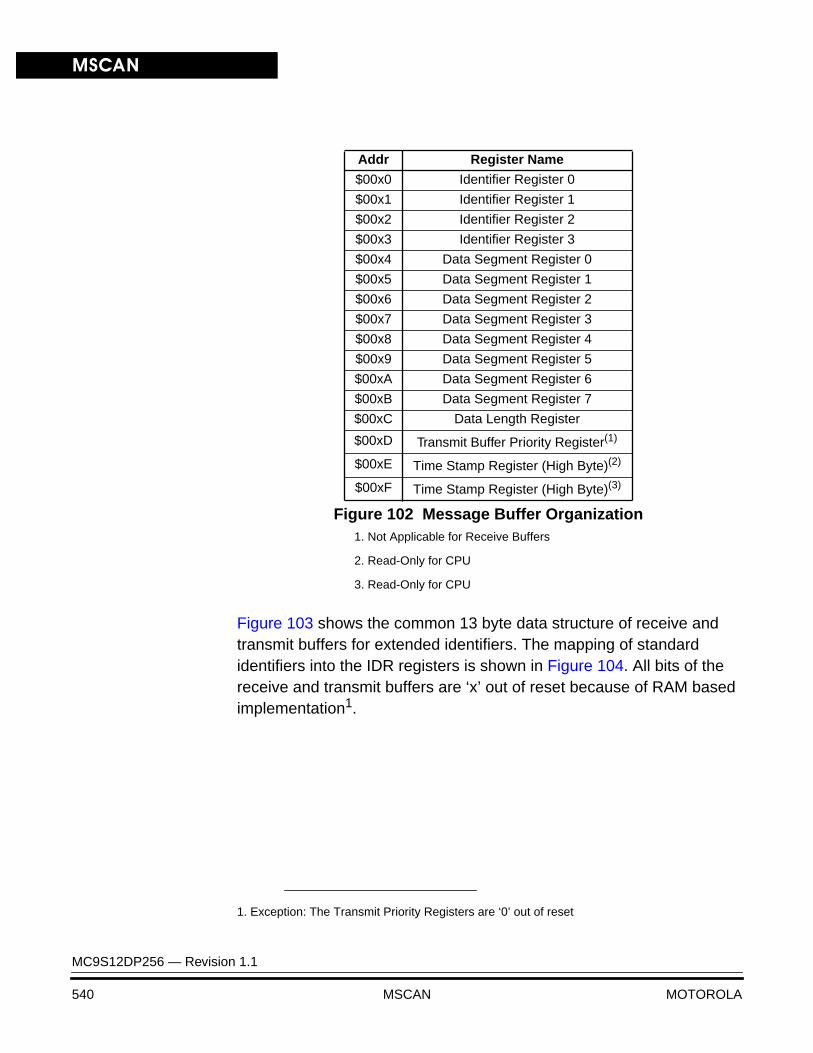
MSCAN
MC9S12DP256 — Revision 1.1
540 MSCAN MOTOROLA
Figure 103 shows the common 13 byte data structure of receive and transmit buffers for extended identifiers. The mapping of standard identifiers into the IDR registers is shown in Figure 104. All bits of the receive and transmit buffers are ‘x’ out of reset because of RAM based implementation1.
Addr Register Name
$00x0 Identifier Register 0
$00x1 Identifier Register 1
$00x2 Identifier Register 2
$00x3 Identifier Register 3
$00x4 Data Segment Register 0
$00x5 Data Segment Register 1
$00x6 Data Segment Register 2
$00x7 Data Segment Register 3
$00x8 Data Segment Register 4
$00x9 Data Segment Register 5
$00xA Data Segment Register 6
$00xB Data Segment Register 7
$00xC Data Length Register
$00xD Transmit Buffer Priority Register(1)
1. Not Applicable for Receive Buffers
$00xE Time Stamp Register (High Byte)(2)
2. Read-Only for CPU
$00xF Time Stamp Register (High Byte)(3)
3. Read-Only for CPU
Figure 102 Message Buffer Organization
1. Exception: The Transmit Priority Registers are ‘0’ out of reset
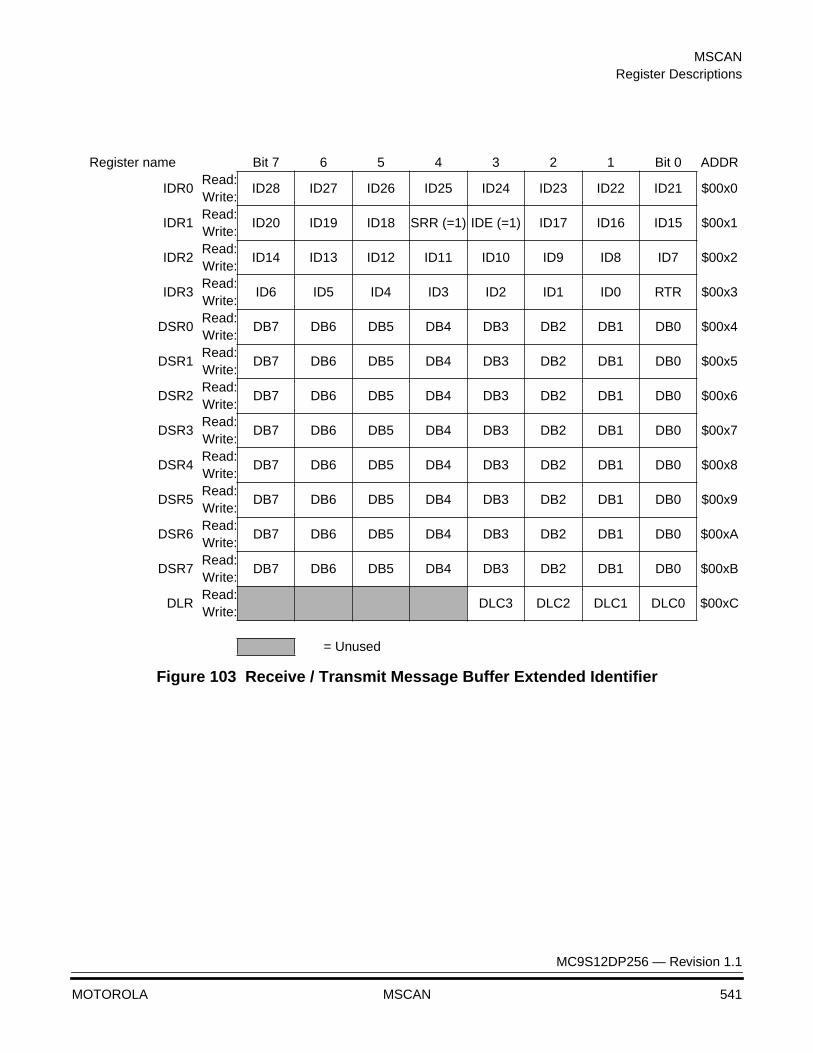
MSCANRegister Descriptions
MC9S12DP256 — Revision 1.1
MOTOROLA MSCAN 541
Register name Bit 7 6 5 4 3 2 1 Bit 0 ADDR
IDR0Read:
ID28 ID27 ID26 ID25 ID24 ID23 ID22 ID21 $00x0Write:
IDR1Read:
ID20 ID19 ID18 SRR (=1) IDE (=1) ID17 ID16 ID15 $00x1Write:
IDR2Read:
ID14 ID13 ID12 ID11 ID10 ID9 ID8 ID7 $00x2Write:
IDR3Read:
ID6 ID5 ID4 ID3 ID2 ID1 ID0 RTR $00x3Write:
DSR0Read:
DB7 DB6 DB5 DB4 DB3 DB2 DB1 DB0 $00x4Write:
DSR1Read:
DB7 DB6 DB5 DB4 DB3 DB2 DB1 DB0 $00x5Write:
DSR2Read:
DB7 DB6 DB5 DB4 DB3 DB2 DB1 DB0 $00x6Write:
DSR3Read:
DB7 DB6 DB5 DB4 DB3 DB2 DB1 DB0 $00x7Write:
DSR4Read:
DB7 DB6 DB5 DB4 DB3 DB2 DB1 DB0 $00x8Write:
DSR5Read:
DB7 DB6 DB5 DB4 DB3 DB2 DB1 DB0 $00x9Write:
DSR6Read:
DB7 DB6 DB5 DB4 DB3 DB2 DB1 DB0 $00xAWrite:
DSR7Read:
DB7 DB6 DB5 DB4 DB3 DB2 DB1 DB0 $00xBWrite:
DLRRead:
DLC3 DLC2 DLC1 DLC0 $00xCWrite:
= Unused
Figure 103 Receive / Transmit Message Buffer Extended Identifier
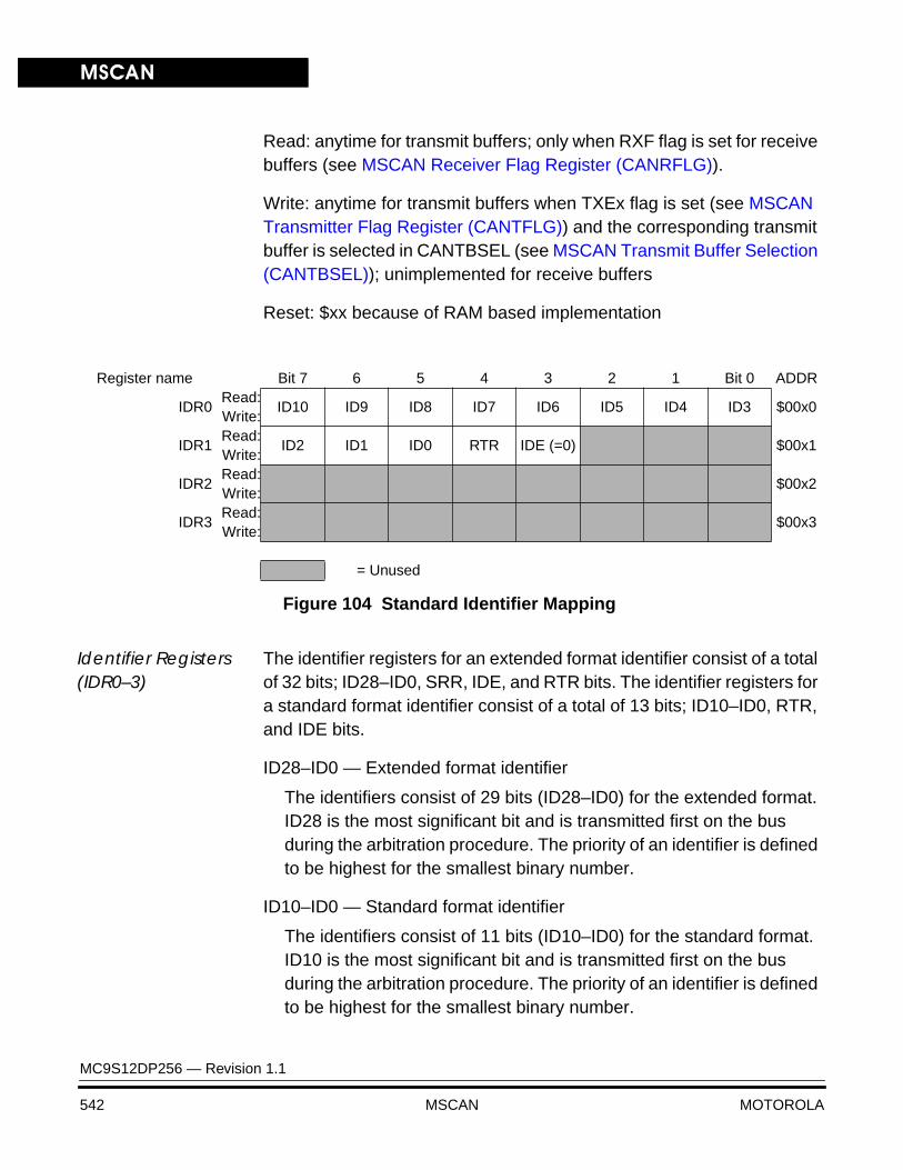
MSCAN
MC9S12DP256 — Revision 1.1
542 MSCAN MOTOROLA
Read: anytime for transmit buffers; only when RXF flag is set for receive buffers (see MSCAN Receiver Flag Register (CANRFLG)).
Write: anytime for transmit buffers when TXEx flag is set (see MSCAN Transmitter Flag Register (CANTFLG)) and the corresponding transmit buffer is selected in CANTBSEL (see MSCAN Transmit Buffer Selection (CANTBSEL)); unimplemented for receive buffers
Reset: $xx because of RAM based implementation
Identifier Registers (IDR0–3)
The identifier registers for an extended format identifier consist of a total of 32 bits; ID28–ID0, SRR, IDE, and RTR bits. The identifier registers for a standard format identifier consist of a total of 13 bits; ID10–ID0, RTR, and IDE bits.
ID28–ID0 — Extended format identifier
The identifiers consist of 29 bits (ID28–ID0) for the extended format. ID28 is the most significant bit and is transmitted first on the bus during the arbitration procedure. The priority of an identifier is defined to be highest for the smallest binary number.
ID10–ID0 — Standard format identifier
The identifiers consist of 11 bits (ID10–ID0) for the standard format. ID10 is the most significant bit and is transmitted first on the bus during the arbitration procedure. The priority of an identifier is defined to be highest for the smallest binary number.
Register name Bit 7 6 5 4 3 2 1 Bit 0 ADDR
IDR0Read:
ID10 ID9 ID8 ID7 ID6 ID5 ID4 ID3 $00x0Write:
IDR1Read:
ID2 ID1 ID0 RTR IDE (=0) $00x1Write:
IDR2Read:
$00x2Write:
IDR3Read:
$00x3Write:
= Unused
Figure 104 Standard Identifier Mapping
MSCANRegister Descriptions
MC9S12DP256 — Revision 1.1
MOTOROLA MSCAN 543
SRR — Substitute Remote Request
This fixed recessive bit is used only in extended format. It must be set to 1 by the user for transmission buffers and is stored as received on the CAN bus for receive buffers.
IDE — ID Extended
This flag indicates whether the extended or standard identifier format is applied in this buffer. In the case of a receive buffer, the flag is set as received and indicates to the CPU how to process the buffer identifier registers. In the case of a transmit buffer, the flag indicates to the MSCAN what type of identifier to send.
1 = Extended format (29 bit)0 = Standard format (11 bit)
RTR — Remote Transmission Request
This flag reflects the status of the Remote Transmission Request bit in the CAN frame. In the case of a receive buffer, it indicates the status of the received frame and supports the transmission of an answering frame in software. In the case of a transmit buffer, this flag defines the setting of the RTR bit to be sent.
1 = Remote frame0 = Data frame
Data Segment Registers (DSR0–7)
The eight data segment registers, each with bits DB7–DB0, contain the data to be transmitted or received. The number of bytes to be transmitted or received is determined by the data length code in the corresponding DLR register.
DB7–DB0 — Data Bits 7–0
Data Length Register (DLR)
This register keeps the data length field of the CAN frame.
DLC3–DLC0 — Data Length Code bits
The data length code contains the number of bytes (data byte count) of the respective message. During the transmission of a remote frame, the data length code is transmitted as programmed while the

MSCAN
MC9S12DP256 — Revision 1.1
544 MSCAN MOTOROLA
number of transmitted data bytes is always 0. The data byte count ranges from 0 to 8 for a data frame. Table 93 shows the effect of setting the DLC bits.
Transmit Buffer Priority Register (TBPR)
This register defines the local priority of the associated message buffer. The local priority is used for the internal prioritization process of the MSCAN and is defined to be highest for the smallest binary number. The MSCAN implements the following internal prioritization mechanisms:
• All transmission buffers with a cleared TXEx flag participate in the prioritization immediately before the SOF (Start of Frame) is sent.
• The transmission buffer with the lowest local priority field wins the prioritization.
• In cases of more than one buffer having the same lowest priority, the message buffer with the lower index number wins.
Read: anytimeWrite: anytime
Table 93 Data length codes
Data length code Data byte
countDLC3 DLC2 DLC1 DLC0
0 0 0 0 0
0 0 0 1 1
0 0 1 0 2
0 0 1 1 3
0 1 0 0 4
0 1 0 1 5
0 1 1 0 6
0 1 1 1 7
1 0 0 0 8
Address Offset: $xxxF
Bit 7 6 5 4 3 2 1 Bit 0
Read:PRIO7 PRIO6 PRIO5 PRIO4 PRIO3 PRIO2 PRIO1 PRIO0
Write:
Reset: 0 0 0 0 0 0 0 0
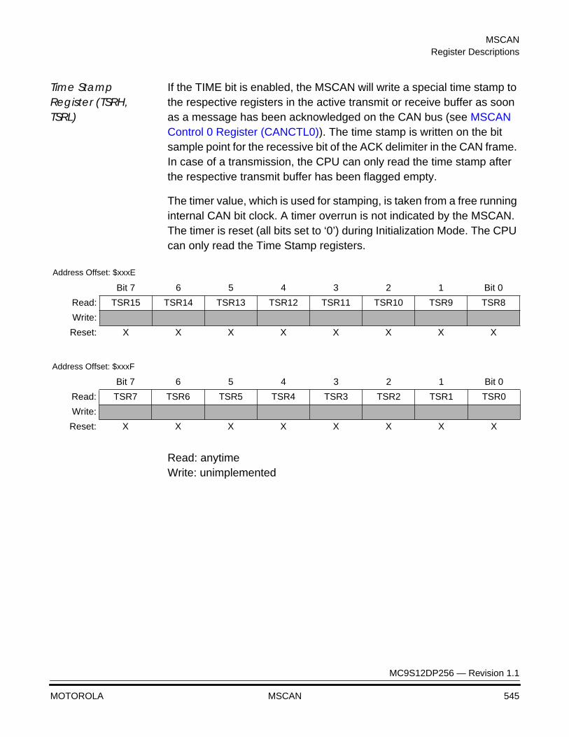
MSCANRegister Descriptions
MC9S12DP256 — Revision 1.1
MOTOROLA MSCAN 545
Time Stamp Register (TSRH, TSRL)
If the TIME bit is enabled, the MSCAN will write a special time stamp to the respective registers in the active transmit or receive buffer as soon as a message has been acknowledged on the CAN bus (see MSCAN Control 0 Register (CANCTL0)). The time stamp is written on the bit sample point for the recessive bit of the ACK delimiter in the CAN frame. In case of a transmission, the CPU can only read the time stamp after the respective transmit buffer has been flagged empty.
The timer value, which is used for stamping, is taken from a free running internal CAN bit clock. A timer overrun is not indicated by the MSCAN. The timer is reset (all bits set to ‘0’) during Initialization Mode. The CPU can only read the Time Stamp registers.
Read: anytimeWrite: unimplemented
Address Offset: $xxxE
Bit 7 6 5 4 3 2 1 Bit 0
Read: TSR15 TSR14 TSR13 TSR12 TSR11 TSR10 TSR9 TSR8
Write:
Reset: X X X X X X X X
Address Offset: $xxxF
Bit 7 6 5 4 3 2 1 Bit 0
Read: TSR7 TSR6 TSR5 TSR4 TSR3 TSR2 TSR1 TSR0
Write:
Reset: X X X X X X X X

MSCAN
MC9S12DP256 — Revision 1.1
546 MSCAN MOTOROLA
Modes of Operation
Normal Modes The MSCAN module behaves as described within this specification in all normal modes.
Special Modes The MSCAN module behaves as described within this specification in all special modes.
Emulation Modes In all emulation modes, the MSCAN module behaves just like normal modes as described within this specification.
Listen-Only Mode In an optional bus monitoring mode (Listen-Only), the CAN node is able to receive valid data frames and valid remote frames, but it sends only ‘recessive’ bits on the CAN bus. In addition it cannot start a transmision. If the MAC sublayer is required to send a ‘dominant’ bit (ACK bit, overload flag, active error flag), the bit is rerouted internally so that the MAC sublayer monitors this ‘dominant bit, although the CAN bus may remain in recessive state externally.
Security Modes The MSCAN module has no security features.
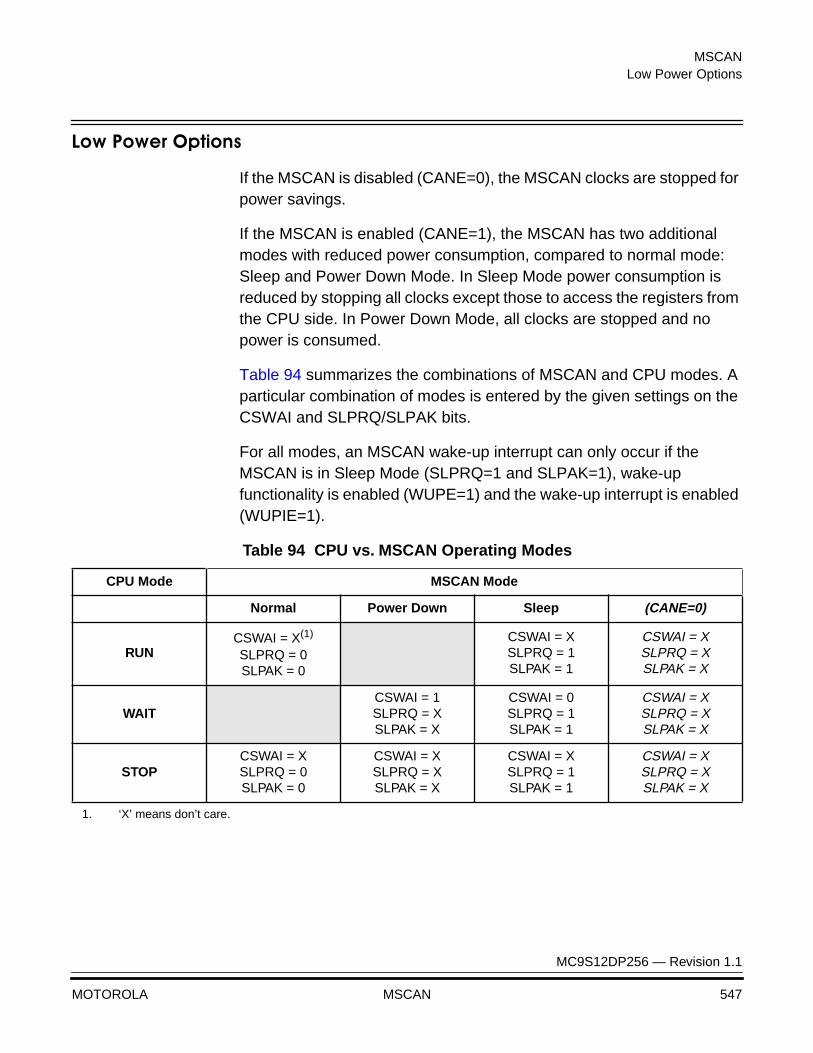
MSCANLow Power Options
MC9S12DP256 — Revision 1.1
MOTOROLA MSCAN 547
Low Power Options
If the MSCAN is disabled (CANE=0), the MSCAN clocks are stopped for power savings.
If the MSCAN is enabled (CANE=1), the MSCAN has two additional modes with reduced power consumption, compared to normal mode: Sleep and Power Down Mode. In Sleep Mode power consumption is reduced by stopping all clocks except those to access the registers from the CPU side. In Power Down Mode, all clocks are stopped and no power is consumed.
Table 94 summarizes the combinations of MSCAN and CPU modes. A particular combination of modes is entered by the given settings on the CSWAI and SLPRQ/SLPAK bits.
For all modes, an MSCAN wake-up interrupt can only occur if the MSCAN is in Sleep Mode (SLPRQ=1 and SLPAK=1), wake-up functionality is enabled (WUPE=1) and the wake-up interrupt is enabled (WUPIE=1).
Table 94 CPU vs. MSCAN Operating Modes
CPU Mode MSCAN Mode
Normal Power Down Sleep (CANE=0)
RUNCSWAI = X(1)
SLPRQ = 0SLPAK = 0
CSWAI = XSLPRQ = 1SLPAK = 1
CSWAI = XSLPRQ = XSLPAK = X
WAITCSWAI = 1SLPRQ = XSLPAK = X
CSWAI = 0SLPRQ = 1SLPAK = 1
CSWAI = XSLPRQ = XSLPAK = X
STOPCSWAI = XSLPRQ = 0SLPAK = 0
CSWAI = XSLPRQ = XSLPAK = X
CSWAI = XSLPRQ = 1SLPAK = 1
CSWAI = XSLPRQ = XSLPAK = X
1. ‘X’ means don’t care.
MSCAN
MC9S12DP256 — Revision 1.1
548 MSCAN MOTOROLA
CPU Run Mode As can be seen in Table 94, only MSCAN Sleep Mode is available as low power option, when CPU is in run mode.
CPU Wait Mode The WAI instruction puts the MCU in a low power consumption stand-by mode. If the CSWAI bit is set, then additional power can be saved in Power Down Mode since the CPU clocks are stopped. After leaving this Power Down Mode the MSCAN restarts its internal controllers and enters Normal Mode again
While the CPU is in Wait Mode, the MSCAN can be operated in Normal Mode and generate interrupts (registers can be accessed via background debug mode). The MSCAN can also operate in any of the low power modes depending on the values of the SLPRQ/SLPAK and CSWAI bits as seen in Table 94.
Stop Mode The STOP instruction puts the MCU in a low power consumption stand-by mode. In Stop mode, the MSCAN operates in Power Down mode regardless of the value of the SLPRQ/SLPAK and CSWAI bits (see CPU vs. MSCAN Operating Modes).
MSCAN Sleep Mode
The CPU can request the MSCAN to enter this low power mode by asserting the SLPRQ bit in the CANCTL0 register. The time when the MSCAN enters Sleep Mode depends on a fixed synchronisation delay and its current activity:
• If it is transmitting, it continues to transmit until the entire message is transmitted and then goes into Sleep Mode.
• If it is receiving, it waits for the end of this message and then goes into Sleep Mode.
• If it is neither transmitting nor receiving, it immediately goes into Sleep Mode.

MSCANLow Power Options
MC9S12DP256 — Revision 1.1
MOTOROLA MSCAN 549
Figure 105 Sleep Request / Acknowledge Cycle
CAUTION: The application software must avoid setting up a transmission (by clearing one or more TXEx flag(s)) and immediately request Sleep Mode (by setting SLPRQ). It depends on the exact sequence of operations whether the MSCAN starts transmitting or goes into Sleep Mode directly.
If Sleep Mode is active, the SLPRQ and SLPAK bits are set (see Figure 105). The application software must use SLPAK as a handshake indication for the request (SLPRQ) to go into Sleep Mode.
When in Sleep Mode (SLPRQ=1 and SLPAK=1), the MSCAN stops its internal clocks. However, clocks to allow register accesses from the CPU side still run. If the MSCAN is in bus-off state, it stops counting the 128*11 consecutive recessive bits due to the stopped clocks. The TxCAN pin remains in a recessive state. If RXF=1, the message can be read and RXF can be cleared. Shifting a new message into the foreground buffer of the receiver FIFO (RxFG) does not take place while in Sleep Mode. It is possible to access the transmit buffers and to clear the associated TXE flags. No message abort takes place while in sleep mode. If the WUPE bit in CANCLT0 is not asserted, the MSCAN will mask any activity it detects on CAN. The RxCAN pin is therefore held internally in a recessive state. This locks the MSCAN in Sleep Mode (see Figure 106).
The MSCAN is only able to leave Sleep Mode (wake-up) when
• bus activity occurs and WUPE=1 or
• the MCU clears the SLPRQ bit
SYNC
SYNC
CPU Clock Domain CAN Clock Domain
MSCANin Sleep Mode
CPUSleep Request
SLPRQFlag
SLPAKFlag
SLPRQ
sync.SLPAK
sync.SLPRQ
SLPAK
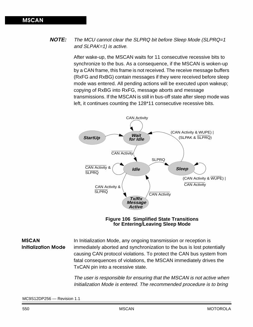
MSCAN
MC9S12DP256 — Revision 1.1
550 MSCAN MOTOROLA
NOTE: The MCU cannot clear the SLPRQ bit before Sleep Mode (SLPRQ=1 and SLPAK=1) is active.
After wake-up, the MSCAN waits for 11 consecutive recessive bits to synchronize to the bus. As a consequence, if the MSCAN is woken-up by a CAN frame, this frame is not received. The receive message buffers (RxFG and RxBG) contain messages if they were received before sleep mode was entered. All pending actions will be executed upon wakeup; copying of RxBG into RxFG, message aborts and message transmissions. If the MSCAN is still in bus-off state after sleep mode was left, it continues counting the 128*11 consecutive recessive bits.
Figure 106 Simplified State Transitionsfor Entering/Leaving Sleep Mode
MSCAN Initialization Mode
In Initialization Mode, any ongoing transmission or reception is immediately aborted and synchronization to the bus is lost potentially causing CAN protocol violations. To protect the CAN bus system from fatal consequences of violations, the MSCAN immediately drives the TxCAN pin into a recessive state.
The user is responsible for ensuring that the MSCAN is not active when Initialization Mode is entered. The recommended procedure is to bring
Wait
Idle
Tx/RxMessageActive
CAN Activity
CAN Activity &
Sleep
SLPRQ
StartUp for Idle
(CAN Activity & WUPE) |
(CAN Activity & WUPE) |(SLPAK & SLPRQ)
CAN Activity
CAN Activity
CAN Activity &
CAN Activity
SLPRQ
SLPRQ
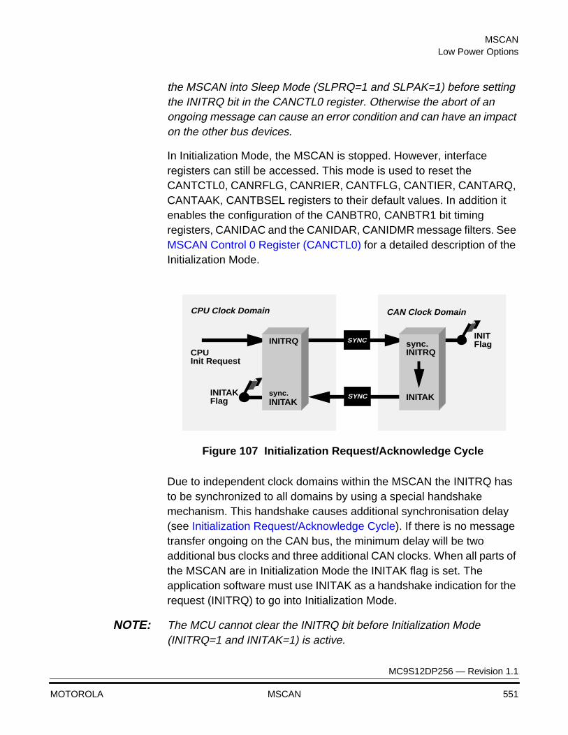
MSCANLow Power Options
MC9S12DP256 — Revision 1.1
MOTOROLA MSCAN 551
the MSCAN into Sleep Mode (SLPRQ=1 and SLPAK=1) before setting the INITRQ bit in the CANCTL0 register. Otherwise the abort of an ongoing message can cause an error condition and can have an impact on the other bus devices.
In Initialization Mode, the MSCAN is stopped. However, interface registers can still be accessed. This mode is used to reset the CANTCTL0, CANRFLG, CANRIER, CANTFLG, CANTIER, CANTARQ, CANTAAK, CANTBSEL registers to their default values. In addition it enables the configuration of the CANBTR0, CANBTR1 bit timing registers, CANIDAC and the CANIDAR, CANIDMR message filters. See MSCAN Control 0 Register (CANCTL0) for a detailed description of the Initialization Mode.
Figure 107 Initialization Request/Acknowledge Cycle
Due to independent clock domains within the MSCAN the INITRQ has to be synchronized to all domains by using a special handshake mechanism. This handshake causes additional synchronisation delay (see Initialization Request/Acknowledge Cycle). If there is no message transfer ongoing on the CAN bus, the minimum delay will be two additional bus clocks and three additional CAN clocks. When all parts of the MSCAN are in Initialization Mode the INITAK flag is set. The application software must use INITAK as a handshake indication for the request (INITRQ) to go into Initialization Mode.
NOTE: The MCU cannot clear the INITRQ bit before Initialization Mode (INITRQ=1 and INITAK=1) is active.
SYNC
SYNC
CPU Clock Domain CAN Clock Domain
CPUInit Request
INITFlag
INITAKFlag
INITRQ
sync.INITAK
sync.INITRQ
INITAK
MSCAN
MC9S12DP256 — Revision 1.1
552 MSCAN MOTOROLA
MSCAN Power Down Mode
The MSCAN is in Power Down Mode when Table 94
• the CPU is in Stop Mode or
• the CPU is in Wait Mode and the CSWAI bit is set.
When entering the Power Down Mode, the MSCAN immediately stops all ongoing transmissions and receptions, potentially causing CAN protocol violations. To protect the CAN bus system from fatal consequences of violations to the above rule, the MSCAN immediately drives the TxCAN pin into a recessive state.
CAUTION: The user is responsible for ensuring that the MSCAN is not active when Power Down Mode is entered. The recommended procedure is to bring the MSCAN into Sleep Mode before the STOP or WAI instruction (if CSWAI is set) is executed. Otherwise the abort of an ongoing message can cause an error condition and can have an impact on the other bus devices.
In Power Down Mode, all clocks are stopped and no registers can be accessed. If the MSCAN was not in Sleep Mode before Power Down Mode became active, the module would perform an internal recovery cycle after powering up. This causes some fixed delay before the module enters Run Mode again.
Programmable Wake-Up Function
The MSCAN can be programmed to wake-up the MSCAN as soon as bus activity is detected (see control bit WUPE in MSCAN Control 0 Register (CANCTL0)). The sensitivity to existing bus action can be modified by applying a low-pass filter function to the RxCAN input line while in Sleep Mode (see control bit WUPM in MSCAN Control 1 Register (CANCTL1)). This feature can be used to protect the MSCAN from wake-up due to short glitches on the CAN bus lines. Such glitches can result e.g. from electromagnetic interference within noisy environments.

MSCANInterrupt Operation
MC9S12DP256 — Revision 1.1
MOTOROLA MSCAN 553
Interrupt Operation
The MSCAN supports four interrupt vectors mapped onto eight different interrupt sources, any of which can be individually masked (for details see sections MSCAN Receiver Flag Register (CANRFLG) to MSCAN Transmitter Interrupt Enable Register (CANTIER)):
• Transmit Interrupt: At least one of the three transmit buffers is empty (not scheduled) and can be loaded to schedule a message for transmission. The TXEx flag of the empty message buffer is set.
• Receive Interrupt: A message is successfully received and shifted into the foreground buffer (RxFG) of the receiver FIFO. This interrupt is generated immediately after receiving the EOF symbol. The RXF flag is set. If there are multiple messages in the receiver FIFO, the RXF flag is set as soon as the next message is shifted to the foreground buffer.
• Wake-Up Interrupt: Activity on the CAN bus occurred during MSCAN internal Sleep Mode and WUPE (see MSCAN Control 0 Register (CANCTL0)) enabled.
• Error Interrupt: An overrun of the receiver FIFO, error or warning condition occurred. The MSCAN Receiver Flag Register (CANRFLG) indicates one of the following conditions:
– Overrun: An overrun condition of the receiver FIFO as described in Receive Structures occurred.
– CAN Status Change: The actual value of the Transmit and Receive Error Counters control the bus state of the MSCAN. As soon as the Error Counters skip into a critical range (Tx/Rx-Warning, Tx/Rx-Error, Bus-Off) the MSCAN flags out an error condition. The status change, which caused the error condition, is indicated within the TSTAT and RSTAT flags (see Receive Structures and MSCAN Receiver Interrupt Enable Register (CANRIER)).
– Bus Off: The Transmit Error Counter has exceeded 255 and MSCAN has gone to Bus-Off state. This flag is redundant with respect to the Can Status Change Interrupt Flag (CSCIF) flag

MSCAN
MC9S12DP256 — Revision 1.1
554 MSCAN MOTOROLA
Interrupt Acknowledge
Interrupts are directly associated with one or more status flags in either the MSCAN Receiver Flag Register (CANRFLG) or the MSCAN Transmitter Flag Register (CANTFLG). Interrupts are pending as long as one of the corresponding flags is set. The flags in the above registers must be reset within the interrupt handler to handshake the interrupt. The flags are reset by writing a ‘1’ to the corresponding bit position. A flag cannot be cleared if the respective condition still prevails.
CAUTION: It must be guaranteed that the CPU only clears the bit causing the current interrupt. For this reason, bit manipulation instructions (BSET) must not be used to clear interrupt flags. These instructions may cause accidental clearing of interrupt flags which are set after entering the current interrupt service routine.
Interrupt Sources The MSCAN supports four interrupt functions as shown in Table 95.
NOTE: The vector addresses and the relative interrupt priority are determined at the MCU level.
Recovery from STOP or WAIT
The MSCAN can recover from STOP or WAIT via the wake-up interrupt. This interrupt can only occur if the MSCAN is in sleep mode (SLPRQ=1 and SLPAK=1), the wake-up option is enabled (WUPE=1) and the wake-up interrupt is enabled (WUPIE=1).
Table 95 MSCAN Interrupt Sources
Interrupt Function Interrupt Flag LocalEnable
Global (CCR)Mask
Wake-Up WUPIF WUPIE
I Bit
ErrorInterrupts
CSCIF CSCIE
OVRIF OVRIE
Receive RXF RXFIE
Transmit
TXE0 TXEIE0
TXE1 TXEIE1
TXE2 TXEIE2
MC9S12DP256 — Revision 1.1
MOTOROLA Analog to Digital Converter 555
Analog to Digital ConverterAnalog to Digital Converter
Contents
Overview . . . . . . . . . . . . . . . . . . . . . . . . . . . . . . . . . . . . . . . . . . . . . . 555Features . . . . . . . . . . . . . . . . . . . . . . . . . . . . . . . . . . . . . . . . . . . . . . 556Block Diagram. . . . . . . . . . . . . . . . . . . . . . . . . . . . . . . . . . . . . . . . . . 557Register Map. . . . . . . . . . . . . . . . . . . . . . . . . . . . . . . . . . . . . . . . . . . 559Functional Description. . . . . . . . . . . . . . . . . . . . . . . . . . . . . . . . . . . . 561Register Descriptions . . . . . . . . . . . . . . . . . . . . . . . . . . . . . . . . . . . . 572External Pin Descriptions . . . . . . . . . . . . . . . . . . . . . . . . . . . . . . . . . 595Reset Initialization . . . . . . . . . . . . . . . . . . . . . . . . . . . . . . . . . . . . . . . 596Modes of Operation. . . . . . . . . . . . . . . . . . . . . . . . . . . . . . . . . . . . . . 597Sample Conversion. . . . . . . . . . . . . . . . . . . . . . . . . . . . . . . . . . . . . . 599General Purpose Input Ports. . . . . . . . . . . . . . . . . . . . . . . . . . . . . . . 602
Overview
This A/D converter is designed as a peripheral bus environment module for the MC9S12DP256 Modular Microcontroller Family. The A/D architecture is a successive approximation architecture that has been used for many years on microcontroller units (MCUs). It is a rugged and proven architecture capable of 10-bit accuracy when operated on-chip with a clocked MCU.
This module is designed to be upwards compatible with the 68HC11 standard 8-bit A/D converters. Many of the operating modes are defined based on the 68HC11 requirements. In addition, there are new operating modes that are unique to the HC12 design.
Analog to Digital Converter
MC9S12DP256 — Revision 1.1
556 Analog to Digital Converter MOTOROLA
Features
• 8/10 Bit Resolution.
• 7 µsec, 10-Bit Single Conversion Time.
• Sample Buffer Amplifier.
• Programmable Sample Time.
• Left/Right Justified, Signed/Unsigned Result Data.
• External Trigger Control.
• Conversion Completion Interrupt Generation.
• Analog Input Multiplexer for 8 Analog Input Channels.
• Analog/Digital Input Pin Multiplexing.
• 1 to 8 Conversion Sequence Lengths.
• Continuous Conversion Mode.
• Multiple Channel Scans.
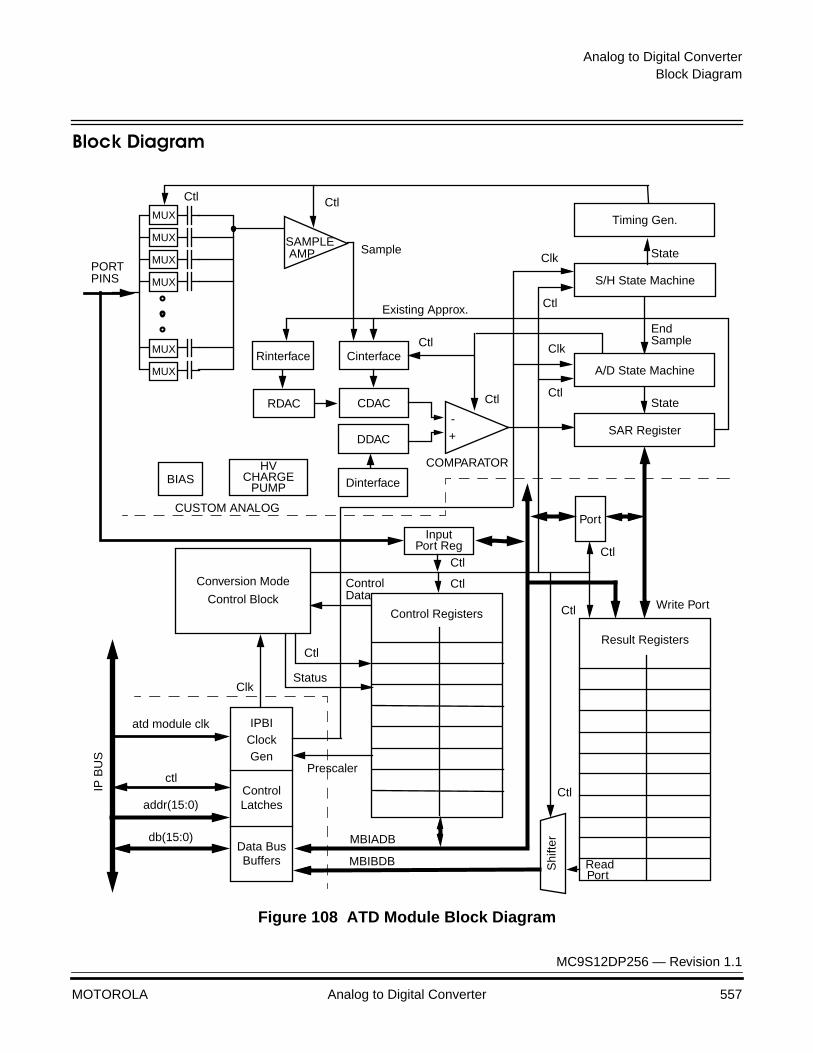
Analog to Digital ConverterBlock Diagram
MC9S12DP256 — Revision 1.1
MOTOROLA Analog to Digital Converter 557
Block Diagram
Figure 108 ATD Module Block Diagram
+-
COMPARATOR
CDAC
DDAC
BIASHV
CHARGEPUMP
MUX
MUX
MUX
MUX
MUX
MUX
PORTPINS
SAMPLE AMP
IPBI
Latches
IP B
US
addr(15:0)
ctl
db(15:0)
InputPort Reg
Data BusBuffers
ClockGen
Control
atd module clk
Result Registers
Shi
fter
RDAC
Rinterface Cinterface
Dinterface
SAR Register
A/D State Machine
Port
Write Port
ReadPort
S/H State Machine
Timing Gen.
Ctl
Ctl
CtlCtl
Ctl
Ctl
Sample
Existing Approx.
EndSample
Control Registers
Conversion Mode
Control Block
Clk
Clk
Clk
Prescaler
ControlData
Ctl
CtlCtl
Ctl
Ctl
Status
State
State
Ctl
MBIADB
MBIBDB
CUSTOM ANALOG

Analog to Digital Converter
MC9S12DP256 — Revision 1.1
558 Analog to Digital Converter MOTOROLA
Functional Block Diagram
The block diagram in Figure 108illustrates the functional structure of the A/D module. The functionality is divided into three submodules as denoted by the dashed lines on the figure. These are the IP Bus Interface, the Conversion Mode Control/Register File, and the Custom Analog.
The IP Bus Interface connects the module to the bus. The objective was to design an ATD module with a generic I/O requirements; this would connect to a particular bus with a specific bus interface. The bus interface contains a clock generation block which clocks the rest of the module. This groups the module’s clocking requirements into one block.
The Conversion Mode Control/Register File defines the HC12 programmers environment for the ATD module. All of the control, status, test, and result registers are located in this submodule. The mechanics that control the various operating modes and scans for the module are implemented here.
The Custom Analog performs analog to digital conversions. It accepts signals from the conversion control machine and the sample machine. This sub-module contains all analog and digital electronics required to perform a single conversion.
A more complete description of each sub-module is provided in the Functional Description section of the specification.
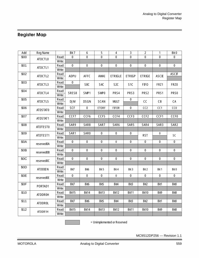
Analog to Digital ConverterRegister Map
MC9S12DP256 — Revision 1.1
MOTOROLA Analog to Digital Converter 559
Register Map
Add Reg Name Bit 7 6 5 4 3 2 1 Bit 0$00
ATDCTL0Read: 0 0 0 0 0 0 0 0Write:
$01ATDCTL1
Read: 0 0 0 0 0 0 0 0Write:
$02ATDCTL2
Read:ADPU AFFC AWAI ETRIGLE ETRIGP ETRIGE ASCIE
ASCIFWrite:
$03ATDCTL3
Read: 0S8C S4C S2C S1C FIFO FRZ1 FRZ0
Write:$04
ATDCTL4Read:
SRES8 SMP1 SMP0 PRS4 PRS3 PRS2 PRS1 PRS0Write:
$05ATDCTL5
Read:DJM DSGN SCAN MULT
0CC CB CA
Write:$06
ATDSTAT0Read: SCF 0 ETORF FIFOR 0 CC2 CC1 CC0
Write:$07
ATDSTAT1Read: CCF7 CCF6 CCF5 CCF4 CCF3 CCF2 CCF1 CCF0Write:
$08ATDTEST0
Read: SAR9 SAR8 SAR7 SAR6 SAR5 SAR4 SAR3 SAR2Write:
$09ATDTEST1
Read: SAR1 SAR0 0 0 0RST
0SC
Write:$0A
reserved0ARead: 0 0 0 0 0 0 0 0Write:
$0Breserved0B
Read: 0 0 0 0 0 0 0 0Write:
$0Creserved0C
Read: 0 0 0 0 0 0 0 0Write:
$0DATDDIEN
Read:Bit7 Bit6 Bit 5 Bit 4 Bit 3 Bit 2 Bit 1 Bit 0
Write:$0E
reserved0ERead: 0 0 0 0 0 0 0 0Write
$0FPORTAD1
Read: Bit7 Bit6 Bit5 Bit4 Bit3 Bit2 Bit1 Bit0Write:
$10ATDDR0H
Read: Bit15 Bit14 Bit13 Bit12 Bit11 Bit10 Bit9 Bit8Write:
$11ATDDR0L
Read: Bit7 Bit6 Bit5 Bit4 Bit3 Bit2 Bit1 Bit0Write:
$12ATDDR1H
Read: Bit15 Bit14 Bit13 Bit12 Bit11 Bit10 Bit9 Bit8Write:
= Unimplemented or Reserved
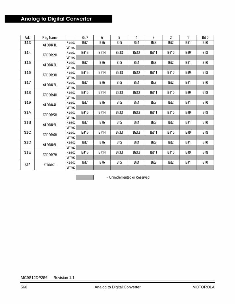
Analog to Digital Converter
MC9S12DP256 — Revision 1.1
560 Analog to Digital Converter MOTOROLA
$13ATDDR1L
Read: Bit7 Bit6 Bit5 Bit4 Bit3 Bit2 Bit1 Bit0Write:
$14ATDDR2H
Read: Bit15 Bit14 Bit13 Bit12 Bit11 Bit10 Bit9 Bit8Write:
$15ATDDR2L
Read: Bit7 Bit6 Bit5 Bit4 Bit3 Bit2 Bit1 Bit0Write:
$16ATDDR3H
Read: Bit15 Bit14 Bit13 Bit12 Bit11 Bit10 Bit9 Bit8Write:
$17ATDDR3L
Read: Bit7 Bit6 Bit5 Bit4 Bit3 Bit2 Bit1 Bit0Write:
$18ATDDR4H
Read: Bit15 Bit14 Bit13 Bit12 Bit11 Bit10 Bit9 Bit8Write:
$19ATDDR4L
Read: Bit7 Bit6 Bit5 Bit4 Bit3 Bit2 Bit1 Bit0Write:
$1AATDDR5H
Read: Bit15 Bit14 Bit13 Bit12 Bit11 Bit10 Bit9 Bit8Write:
$1BATDDR5L
Read: Bit7 Bit6 Bit5 Bit4 Bit3 Bit2 Bit1 Bit0Write:
$1CATDDR6H
Read: Bit15 Bit14 Bit13 Bit12 Bit11 Bit10 Bit9 Bit8Write:
$1DATDDR6L
Read: Bit7 Bit6 Bit5 Bit4 Bit3 Bit2 Bit1 Bit0Write:
$1EATDDR7H
Read: Bit15 Bit14 Bit13 Bit12 Bit11 Bit10 Bit9 Bit8Write:
$1F ATDDR7LRead: Bit7 Bit6 Bit5 Bit4 Bit3 Bit2 Bit1 Bit0Write:
Add Reg Name Bit 7 6 5 4 3 2 1 Bit 0
= Unimplemented or Reserved
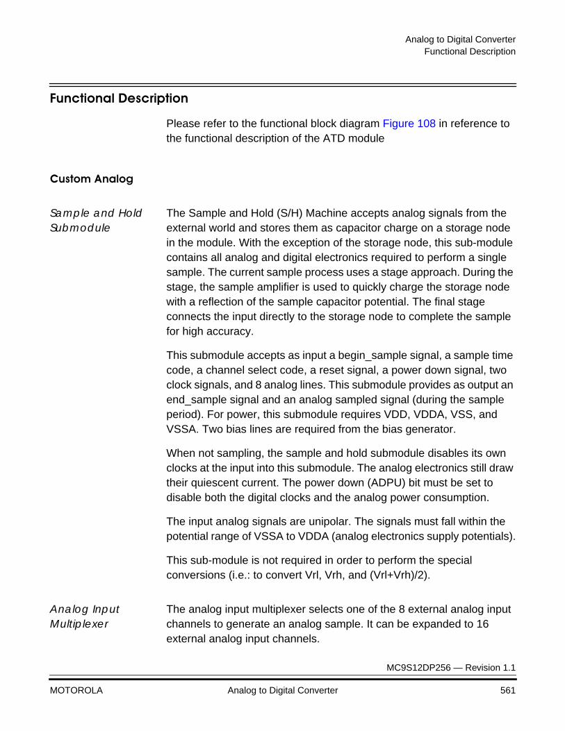
Analog to Digital ConverterFunctional Description
MC9S12DP256 — Revision 1.1
MOTOROLA Analog to Digital Converter 561
Functional Description
Please refer to the functional block diagram Figure 108 in reference to the functional description of the ATD module
Custom Analog
Sample and Hold Submodule
The Sample and Hold (S/H) Machine accepts analog signals from the external world and stores them as capacitor charge on a storage node in the module. With the exception of the storage node, this sub-module contains all analog and digital electronics required to perform a single sample. The current sample process uses a stage approach. During the stage, the sample amplifier is used to quickly charge the storage node with a reflection of the sample capacitor potential. The final stage connects the input directly to the storage node to complete the sample for high accuracy.
This submodule accepts as input a begin_sample signal, a sample time code, a channel select code, a reset signal, a power down signal, two clock signals, and 8 analog lines. This submodule provides as output an end_sample signal and an analog sampled signal (during the sample period). For power, this submodule requires VDD, VDDA, VSS, and VSSA. Two bias lines are required from the bias generator.
When not sampling, the sample and hold submodule disables its own clocks at the input into this submodule. The analog electronics still draw their quiescent current. The power down (ADPU) bit must be set to disable both the digital clocks and the analog power consumption.
The input analog signals are unipolar. The signals must fall within the potential range of VSSA to VDDA (analog electronics supply potentials).
This sub-module is not required in order to perform the special conversions (i.e.: to convert Vrl, Vrh, and (Vrl+Vrh)/2).
Analog Input Multiplexer
The analog input multiplexer selects one of the 8 external analog input channels to generate an analog sample. It can be expanded to 16 external analog input channels.
Analog to Digital Converter
MC9S12DP256 — Revision 1.1
562 Analog to Digital Converter MOTOROLA
The analog input multiplexer includes negative stress protection circuitry which prevents crosstalk between channels when the applied input potentials are within specification.
Sample Buffer Amplifier
The sample amplifier is used to buffer the input analog signal so that the storage node can be quickly charged to the sample potential.
Limitations The current ATD module architecture allows for only one sample storage node which is located in the A/D machine. As a result, only one sample can be held at a time; this means the S/H machine and the A/D machine cannot run concurrently even though they are independent machines. The minimum conversion time is therefore dependent on the program selection of the sample time. The current minimum conversion time specification uses the minimum sample time.
No DC level correction, channel to channel gain adjust, or other data acquisition functions are currently performed on the input analog signals.
Analog-to-Digital Converter Submodule
The Analog-to-Digital (A/D) Machine performs analog to digital conversions. The resolution of the A/D converter is program selectable at either 8 or 10 bits. This machine uses a successive approximation A/D architecture. It functions by comparing the stored analog sample potential with a series of digitally generated analog potentials. By following a binary search algorithm, the converter locates the approximating potential that is nearest to the sampled potential.
This submodule contains all the necessary analog and digital electronics to perform a single analog to digital conversion. This module accepts as input a begin_sample signal, an end_sample signal, a 8/10 bit resolution select line, a special conversion select line, a two wire conversion type bus, a reset signal, a power down signal, a clock signal, an input analog signal, and two reference potentials. This submodule provides as output a 10-bit digital word and an end_convert signal as outputs. For power, this submodule requires VDD, VDDA, VSS, VSSA. and Vhv (the in-module generated high voltage potential). One bias line is required from the bias generator.
Analog to Digital ConverterFunctional Description
MC9S12DP256 — Revision 1.1
MOTOROLA Analog to Digital Converter 563
When not sampling, the analog-to-digital submodule disables its own clocks at the input into this submodule. The analog electronics still draws quiescent current. The power down (ADPU) bit must be set to disable both the digital clocks and the analog power consumption.
Note that only analog input signals within the potential range of VRL to VRH (A/D reference potentials) will result in a non-railed digital output codes.
This sub-module performs special test conversions internally without the aid of the sample submodule (i.e.: to convert VRL, VRH, and (VRL+VRH)/2).
Resistor and Capacitor DAC Arrays
The A/D core is a 10 bit analog to digital converter implemented in a0.25 micron CMOS process capable of being manufactured in numer-ous foundries without detrimental affects. It must also be capable ofaccepting 5 volts inputs without permanent damage while simulta-neously operating at 5 volts. This can be rather challenging.
The heart of the converter consist of a combination of resistors and capacitors. In particular, a thermometer code 7 bit resistor string for the MSB and 3 bits of capacitors to determine the LSB. The chip presently operates with a single-ended signal but can be modified for a sign bit which would allow for negative signals.
The design is a 10 bit single ended design using a “pseudo” differential scheme. The first 7 MSB bits consist of a 1 of 128 resistor string. The remaining 3 LSB bits are binary weighted capacitor of value 8c, 4c, 2c, and 1c. The last C is an extra C which can be used for offset compensation of + 1/2 LSB.
Comparator The comparator is a three stage comparator. The first two stages are capacitively coupled, differential comparator stages; these add a fixed gain to the comparison signal. The last stage is a clocked regenerative comparator stage; this stage drives the input comparison signal to the operating potential rails. The input offset voltage of the comparator is removed from the stored sample by zeroing the comparator before the sample process. The gain required by the comparator for 10-bit accuracy is greater than 60dB.

Analog to Digital Converter
MC9S12DP256 — Revision 1.1
564 Analog to Digital Converter MOTOROLA
A/D State Machine and SAR (Successive Approximation Register)
The A/D state machine controls the conversion process in the A/D converter. The machine needs to know when a sample period is occurring since the sample storage node is located on the CDAC capacitor array. The machine works closely with the SAR to perform a binary search algorithm. The intermediate results in the SAR are used by the CDAC and RDAC interface circuits to determine which switches to set to generate the next approximation potential. At the end of the conversion process, the SAR contains the nearest approximation to the sampled signal given the resolution of the A/D converter.
Limitations The specification minimum conversion time is set by the settling time of the digitally generated compare potentials. The settling time is limited by the RC time constant of the RDAC/CDAC arrays. Basically it takes 2 clocks to settle. So the time constant is approximately 1 µsec.
Conversion Mode Control and Register File
This section defines the programmer interface to the ATD module. The register file defines the address space used to access the module’s controls, status, and data. The conversion mode control uses the control register settings to define the overall flow of the ATD module’s operations.
Control/Status Registers and Control Section
There are eight control registers and three status registers associated with the ATD module. IP bus writes to ATDCTL4&5 registers initiate a new conversion sequence. If a conversion sequence is already running, this sequence will be aborted and a new sequence will be begun.
The Mode Control communicates with the S/H machine and the A/D machine when necessary to collect samples and perform conversions. The Mode Control issues a “begin_sample” signal which for a normal conversion signals the S/H machine to begin collecting a sample and for the A/D machine to begin receiving a sample. At the end of the sample period, the S/H machine issues a end_sample signal which signals the A/D machine to begin the analog to digital conversion process. The conversion process is terminated when the A/D machine issues an end_convert signal back to the Mode Control unit. For special test mode conversions (VRL, VRH, (VRL+VRH)/2), the sample machine is important because it generates an end_sample signal; the A/D machine uses the
Analog to Digital ConverterFunctional Description
MC9S12DP256 — Revision 1.1
MOTOROLA Analog to Digital Converter 565
reference potentials to set the sampled signal level within itself without relying on the sample machine to deliver them.
Mode Control organizes the conversion sequences, specifies the input sample channel, implements the external trigger mode, and move digital output data from the SAR to the result registers. One important task is to control register file read/write timing to avoid conflicts between IP bus accesses and ATD module updates to the same register at the same time.
The result registers consists of two port latches. The SAR writes data into the register through one port; the module data bus reads data out of the registers through the other port.
External Trigger Input (ETRIG)
The external trigger feature allows the user to synchronize ATD conversions to the external environment events rather than relying on software to signal the ATD module when ATD conversions are to take place. The input signal is programmable to be edge or level sensitive with polarity control. If level sensitivity is selected the atd_etrig input signal is treated like a trigger gate.
In edge trigger mode the active edge of the external trigger signal is used to signal the ATD module when to begin sampling the input.
A summary of the external trigger function is shown in Table 96. This table gives a brief description of the different combinations of control bits and their affect on the external trigger function.
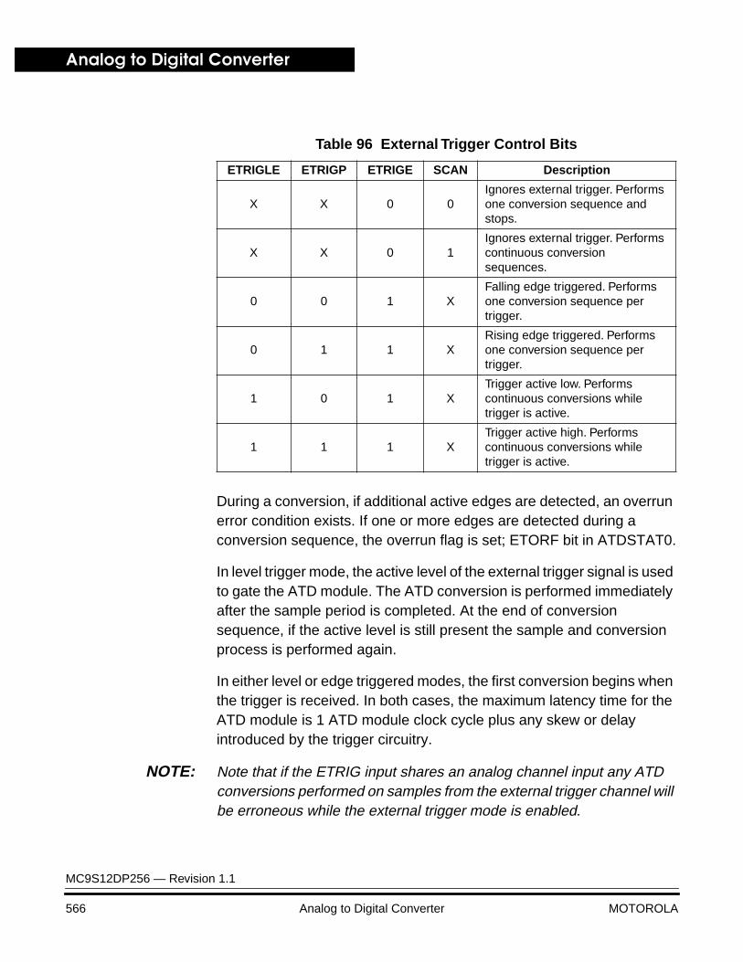
Analog to Digital Converter
MC9S12DP256 — Revision 1.1
566 Analog to Digital Converter MOTOROLA
During a conversion, if additional active edges are detected, an overrun error condition exists. If one or more edges are detected during a conversion sequence, the overrun flag is set; ETORF bit in ATDSTAT0.
In level trigger mode, the active level of the external trigger signal is used to gate the ATD module. The ATD conversion is performed immediately after the sample period is completed. At the end of conversion sequence, if the active level is still present the sample and conversion process is performed again.
In either level or edge triggered modes, the first conversion begins when the trigger is received. In both cases, the maximum latency time for the ATD module is 1 ATD module clock cycle plus any skew or delay introduced by the trigger circuitry.
NOTE: Note that if the ETRIG input shares an analog channel input any ATD conversions performed on samples from the external trigger channel will be erroneous while the external trigger mode is enabled.
Table 96 External Trigger Control Bits
ETRIGLE ETRIGP ETRIGE SCAN Description
X X 0 0Ignores external trigger. Performs one conversion sequence and stops.
X X 0 1Ignores external trigger. Performs continuous conversion sequences.
0 0 1 XFalling edge triggered. Performs one conversion sequence per trigger.
0 1 1 XRising edge triggered. Performs one conversion sequence per trigger.
1 0 1 XTrigger active low. Performs continuous conversions while trigger is active.
1 1 1 XTrigger active high. Performs continuous conversions while trigger is active.
Analog to Digital ConverterFunctional Description
MC9S12DP256 — Revision 1.1
MOTOROLA Analog to Digital Converter 567
The external trigger input is enabled by the ETRIGE, ETRIGP, ETRIGLE control bits in ATDCTL2. When ETRIGE is first enabled, a conversion sequence is initiated by an external event transitioning the ETRIG pin. Once ETRIGE is enabled, conversions cannot be started by a write to ATDCTL5, but rather must be triggered externally.
External trigger mode operates with the other operating modes to produce a variety of external triggered modes. For example, by selecting a conversion sequence length of one, the ATD module can be made to perform a single conversion per active edge of the external trigger. Since, interrupts can be generated by the end of the sequence, this mode will signal the MCU after single external events. By selecting a larger conversion sequence length, an entire sequence of conversions can be performed on one external trigger event.
If the level mode is active and the external trigger both de-asserts and re-asserts itself during a conversion sequence, this does not constitute an overrun. Therefore, the flag is not set. If the trigger is left asserted in level mode while a sequence is completing, another sequence will be triggered immediately. If the level sensitive mode is selected and ETRIG input is held active, subsequent conversion sequences occur after the sequence complete flag is set.
General Purpose Digital Input Port Operation
The input channel pins can be multiplexed between analog and digital data. As analog inputs, they are multiplexed and sampled to supply signals to the A/D converter. As digital inputs, they supply external input data that can be accessed through the digital port registers.
The analog/digital multiplex operation is performed in the input pads. The input pad is always connected to the analog inputs of the ATD module. The input pad signal is buffered before the data is bussed to the digital port registers. The buffer is a schmitt trigger nand so that the buffer can be turned off; this is important so that the buffer does not draw excess current when analog potentials are presented at its input. This is particularly important when some of the inputs are being used as digital inputs and some as analog inputs. To minimize excess current draw, the buffer is enabled only if the respective ATDDIEN bit is set. If this bit is not set a digital read will always return a “1”. Analog signals present on

Analog to Digital Converter
MC9S12DP256 — Revision 1.1
568 Analog to Digital Converter MOTOROLA
the input pins at the digital sampling time that don’t meet the VIL or VIH specification will return unknown digital values. A read of the PORTAD1 may affect the accuracy of an in progress sample period but will not affect an in progress A/D conversion.
There is a digital, 8-bit, input-only port associated with the ATD. It is accessed through the 8-bit Port Data Register (PORTAD1). The number of bits utilized in the port register depends on the number of analog channels implemented with the 8 channel ATD module.
Clock Prescale Function
To keep the ATD module’s conversion clock within the specified frequency range, a clock prescale function is available. This function divides the ATD module clock by a program selectable binary constant in order to generate the ATD module’s conversion clock. The ATD conversion clock is used to clock both the sample machine and the A/D machine.
Another important benefit of the prescaled clock feature is that it allows the user control over the sample period. Note that if the prescale function is used this way, the conversion time is also affected.
The prescale feature is based on a 5 bit modulus counter and will divide the clock by an integer value between 1 and 32. The final clock frequency is obtained with a further division by 2. Therefore, the highest possible ATD conversion clock frequency is one half of the ATD module clock frequency, but cannot be faster than the maximum ATD operating frequency as defined in the electrical specification. The maximum speed of ATD conversion frequency is 2 MHz. Table 102 lists the prescale value for various setting of the control register bits. Figure 109 is a block diagram of the clock prescale logic.
The ATD conversion clock and the ATD module clock have a direct phase relationship. However, the ATD module operates as if it is effectively asynchronous to IP bus cycles.
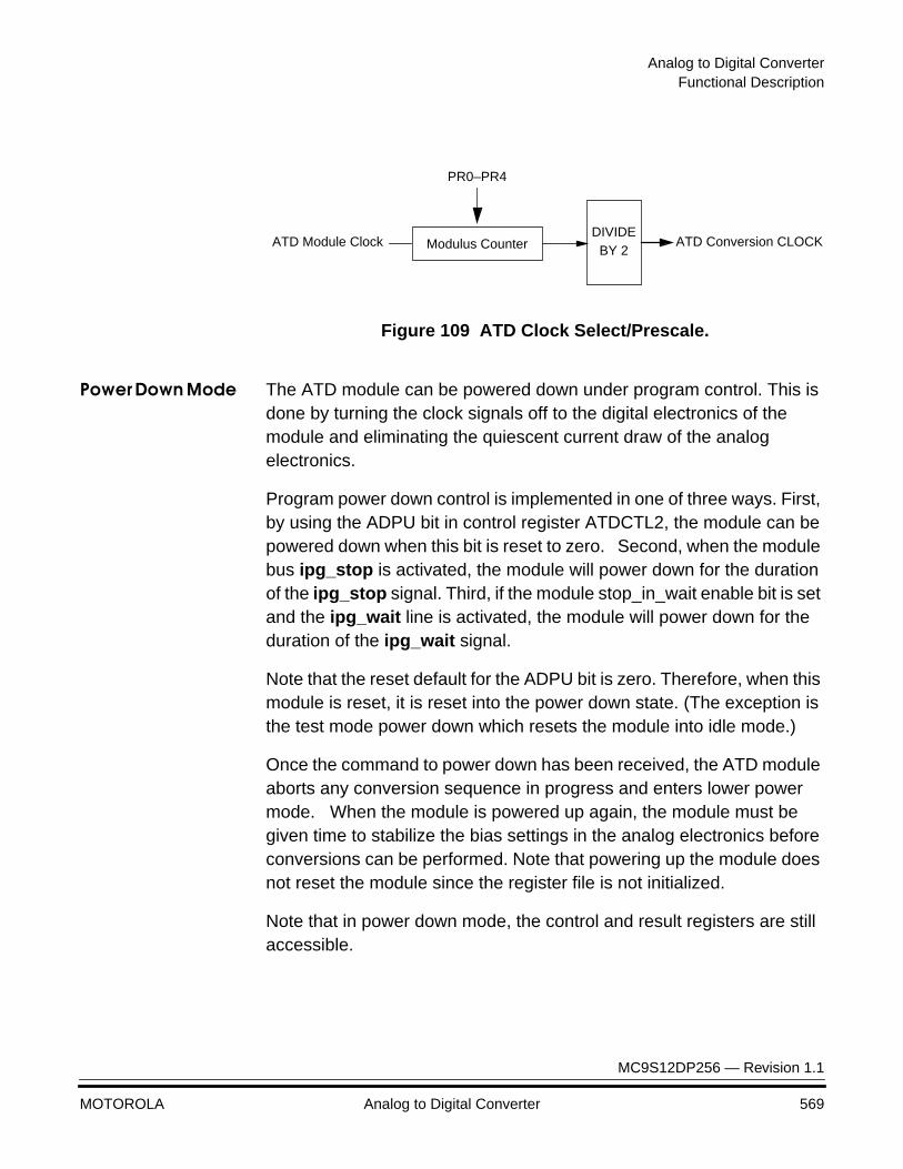
Analog to Digital ConverterFunctional Description
MC9S12DP256 — Revision 1.1
MOTOROLA Analog to Digital Converter 569
Figure 109 ATD Clock Select/Prescale.
Power Down Mode The ATD module can be powered down under program control. This is done by turning the clock signals off to the digital electronics of the module and eliminating the quiescent current draw of the analog electronics.
Program power down control is implemented in one of three ways. First, by using the ADPU bit in control register ATDCTL2, the module can be powered down when this bit is reset to zero. Second, when the module bus ipg_stop is activated, the module will power down for the duration of the ipg_stop signal. Third, if the module stop_in_wait enable bit is set and the ipg_wait line is activated, the module will power down for the duration of the ipg_wait signal.
Note that the reset default for the ADPU bit is zero. Therefore, when this module is reset, it is reset into the power down state. (The exception is the test mode power down which resets the module into idle mode.)
Once the command to power down has been received, the ATD module aborts any conversion sequence in progress and enters lower power mode. When the module is powered up again, the module must be given time to stabilize the bias settings in the analog electronics before conversions can be performed. Note that powering up the module does not reset the module since the register file is not initialized.
Note that in power down mode, the control and result registers are still accessible.
Modulus CounterDIVIDE
BY 2
PR0–PR4
ATD Conversion CLOCKATD Module Clock

Analog to Digital Converter
MC9S12DP256 — Revision 1.1
570 Analog to Digital Converter MOTOROLA
Background Debug (ATD FREEZE) Mode
When debugging an application, it is useful to have the ATD pause when a breakpoint is encountered. To accommodate this, there are two FREEZE bits in the ATDCTL3 register used to select one of three responses: First, the ATD module may ignore the background signal. Second, it may respond to the freeze request by finishing the current conversion and freezing before starting the next sample period. Third, it may respond by immediately freezing.
The FREEZE state is implemented by stopping the ATD clock when the module background signal is asserted. Control and timing logic is static allowing the register contents and timing position to be remembered indefinitely. The analog electronics remains powered up; however, leakage onto the storage node and comparator reference capacitors may compromise the accuracy of a frozen conversion depending on the length of the freeze period. When the background signal is negated, clock activity resumes. The bus interface remains active to allow module access to the ATD register block during the frozen period.
Module Reset The ATD module is reset on two different events. First, if the IP bus master reset signal is activated, the ATD module is reset. Second, if the RST bit in the ATDTEST register is activated, the ATD module is reset. The single difference between the two events is that the RST bit event does not reset the ADPU bit to its reset state value - i.e.: the module is not reset into a powered down state.
The ATD module reset function places the module back into an initialized state. If the module is performing a conversion sequence, both the current conversion and the sequence are terminated. The conversion complete flags are cleared and any pending interrupts are cancelled. Note that the control, test, and status registers are initialized on reset; the initialized register state is defined in the register description section of this specification.
The ATD module is powered down on reset (except for the RST bit reset event). This occurs as a function of the register file initialization; the reset definition of the ADPU bit (power down bit) is zero or powered down. Note the RST bit reset event does not reset the ADPU bit to its reset value so the module will be returned to an idle state following this reset triggering event.
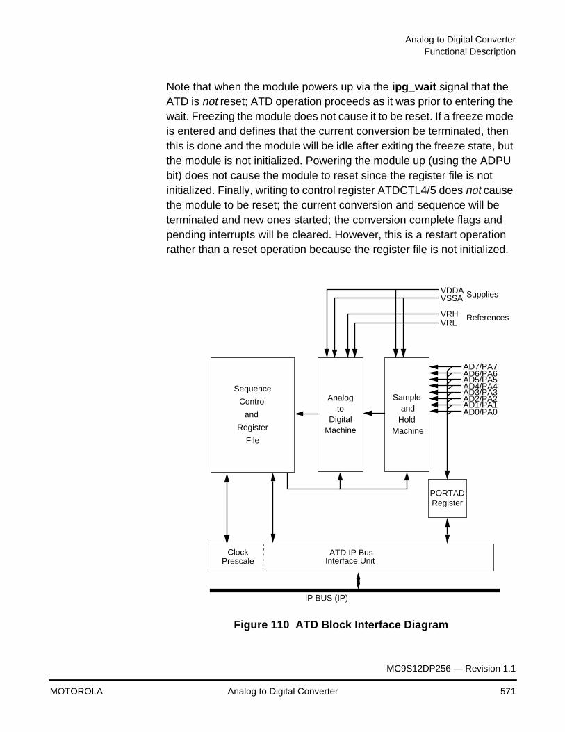
Analog to Digital ConverterFunctional Description
MC9S12DP256 — Revision 1.1
MOTOROLA Analog to Digital Converter 571
Note that when the module powers up via the ipg_wait signal that the ATD is not reset; ATD operation proceeds as it was prior to entering the wait. Freezing the module does not cause it to be reset. If a freeze mode is entered and defines that the current conversion be terminated, then this is done and the module will be idle after exiting the freeze state, but the module is not initialized. Powering the module up (using the ADPU bit) does not cause the module to reset since the register file is not initialized. Finally, writing to control register ATDCTL4/5 does not cause the module to be reset; the current conversion and sequence will be terminated and new ones started; the conversion complete flags and pending interrupts will be cleared. However, this is a restart operation rather than a reset operation because the register file is not initialized.
Figure 110 ATD Block Interface Diagram
IP BUS (IP)
AD0/PA0AD1/PA1AD2/PA2AD3/PA3AD4/PA4AD5/PA5AD6/PA6AD7/PA7
ATD IP BusInterface Unit
VRHVRL
Sample and
PORTADRegister
References
VDDAVSSA
Hold Machine
Supplies
Analogto
DigitalMachine
ClockPrescale
Sequence
Control
and
Register
File
Analog to Digital Converter
MC9S12DP256 — Revision 1.1
572 Analog to Digital Converter MOTOROLA
Register Descriptions
Register Arrangement and IP Address Mapping
The base address of the module is hardware programmable. The ATD register map is fixed and begins at the module’s base address. Figure 111 summarizes the ATD module’s address space. The following subsections describe the bit-level arrangement and functionality of each register.
The ATD module is clocked by the ATD module clock. The module signals valid output data to the MCU via interrupts or conversion complete flags. Therefore, it does not need a synchronizing signal to inform the CPU of conversion complete.
The module has two internal buses with which to move control, status, and result data between internal registers and the IP bus. The IP bus controls activity on these internal buses based on bus requests to the ATD module. The ATD module moves result data into the dual ported result registers through a separate dedicated result bus to avoid collisions with IP bus accesses. Special attention is paid so that IP bus accesses to the ATD register file do not conflict with module updates to the same register at the same time.
When control bits are written by the IP bus, they update the control register immediately. If an A/D conversion is in progress, the results are not guaranteed until the next A/D conversion cycle begins.
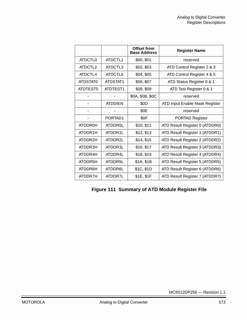
Analog to Digital ConverterRegister Descriptions
MC9S12DP256 — Revision 1.1
MOTOROLA Analog to Digital Converter 573
Figure 111 Summary of ATD Module Register File
Offset from Base Address Register Name
ATDCTL0 ATDCTL1 $00, $01 reserved
ATDCTL2 ATDCTL3 $02, $03 ATD Control Register 2 & 3
ATDCTL4 ATDCTL5 $04, $05 ATD Control Register 4 & 5
ATDSTAT0 ATDSTAT1 $06, $07 ATD Status Register 0 & 1
ATDTEST0 ATDTEST1 $08, $09 ATD Test Register 0 & 1
- - $0A, $0B, $0C reserved
- ATDDIEN $0D ATD Input Enable Mask Register
- - $0E reserved
- PORTAD1 $0F PORTAD Register
ATDDR0H ATDDR0L $10, $11 ATD Result Register 0 (ATDDR0)
ATDDR1H ATDDR1L $12, $13 ATD Result Register 1 (ATDDR1)
ATDDR2H ATDDR2L $14, $15 ATD Result Register 2 (ATDDR2)
ATDDR3H ATDDR3L $16, $17 ATD Result Register 3 (ATDDR3)
ATDDR4H ATDDR4L $18, $19 ATD Result Register 4 (ATDDR4)
ATDDR5H ATDDR5L $1A, $1B ATD Result Register 5 (ATDDR5)
ATDDR6H ATDDR6L $1C, $1D ATD Result Register 6 (ATDDR6)
ATDDR7H ATDDR7L $1E, $1F ATD Result Register 7 (ATDDR7)
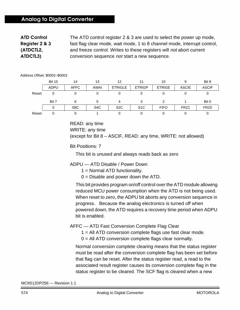
Analog to Digital Converter
MC9S12DP256 — Revision 1.1
574 Analog to Digital Converter MOTOROLA
ATD Control Register 2 & 3 (ATDCTL2, ATDCTL3)
The ATD control register 2 & 3 are used to select the power up mode, fast flag clear mode, wait mode, 1 to 8 channel mode, interrupt control, and freeze control. Writes to these registers will not abort current conversion sequence nor start a new sequence.
READ: any timeWRITE: any time (except for Bit 8 – ASCIF, READ: any time, WRITE: not allowed)
Bit Positions: 7
This bit is unused and always reads back as zero
ADPU — ATD Disable / Power Down1 = Normal ATD functionality.0 = Disable and power down the ATD.
This bit provides program on/off control over the ATD module allowing reduced MCU power consumption when the ATD is not being used. When reset to zero, the ADPU bit aborts any conversion sequence in progress. Because the analog electronics is turned off when powered down, the ATD requires a recovery time period when ADPU bit is enabled.
AFFC — ATD Fast Conversion Complete Flag Clear1 = All ATD conversion complete flags use fast clear mode.0 = All ATD conversion complete flags clear normally.
Normal conversion complete clearing means that the status register must be read after the conversion complete flag has been set before that flag can be reset. After the status register read, a read to the associated result register causes its conversion complete flag in the status register to be cleared. The SCF flag is cleared when a new
Address Offset: $0002–$0003
Bit 15 14 13 12 11 10 9 Bit 8
ADPU AFFC AWAI ETRIGLE ETRIGP ETRIGE ASCIE ASCIF
Reset: 0 0 0 0 0 0 0 0
Bit 7 6 5 4 3 2 1 Bit 0
0 S8C S4C S2C S1C FIFO FRZ1 FRZ0
Reset: 0 0 1 0 0 0 0 0
Analog to Digital ConverterRegister Descriptions
MC9S12DP256 — Revision 1.1
MOTOROLA Analog to Digital Converter 575
conversion sequence is begun by writing to control register ATDCTL4/5. In application where the ATD module is being polled to determine if an ATD conversion is complete, this feature provides a convenient way of clearing the status register conversion complete flag.
In applications where ATD interrupts are used to signal conversion completion, the precondition of reading the status register can be eliminated – hence the fast conversion complete flag clear mode. In this mode, any access to a result register will cause its associated conversion complete flag in the status register to be cleared. The SCF flag is cleared after the first (any) result register is read.
AWAI — ATD Wait Mode1 = Enable ATD wait function during MCU Wait mode.0 = Disable ATD wait function.
The wait function allows the MCU to selectively halt and power down the ATD module. If the AWAI bit is set and the MCU asserts the IP bus wait_mode, then the ATD module immediately halts operation and powers down. When the wait_mode is released, the ATD module powers up and continues operation. The module is not reset; the register file is not initialized; the conversion sequence is not restarted. If the AWAI is reset (zero), then the ATD module ignores the wait_mode line.
ETRIGLE — External Trigger Level/Edge control
This bit sets the mode of the incoming external trigger signal1 = Level mode – active level gates ATD operation0 = Edge mode – active edge mode
ETRIGP — External Trigger Polarity
This bit controls the polarity of the external trigger signal1 = Active high level or rising edge active0 = Active low level or falling edge active
ETRIGE — External Trigger Mode enable1 = Enable external trigger mode0 = Disable external trigger mode.

Analog to Digital Converter
MC9S12DP256 — Revision 1.1
576 Analog to Digital Converter MOTOROLA
External trigger mode allows the user to synchronize sample and ATD conversions processes with external events.
External Gated Continuous-Scan Mode is defined when the SCAN and ETRIGLE bits are set. It allows the user to synchronize the conversion process with external events and control the number of conversion performed in sequence. The ETRIG active level initiates a conversion and at the end of the conversion if the ETRIGE bit is active another sample is initiated.
Note that the conversion results for the external trigger channel have no meaning while external trigger mode is enabled.
ASCIE — ATD Sequence Complete Interrupt Enable 1 = Enables ATD interrupt on Sequence Complete.0 = Disables ATD interrupt.
The sequence complete interrupt function signals the MCU when a conversion sequence is complete. At this time, the result registers contain the result data generated by the conversion sequence. If this interrupt function is disabled, then the conversion complete flags must be polled to determine when a conversion or a conversion sequence is complete. Note that reset clears pending interrupts.
ASCIF — ATD Sequence Complete Interrupt Flag1 = ATD sequence complete interrupt occurred.0 = No ATD sequence complete interrupt occurred.
Table 97 Left Justified, Signed and Unsigned ATD Output Codes
Input SignalVrl = 0 Volts
Vrh = 5.12 Volts
Signed8-Bit
Codes
Unsigned8-Bit
Codes
Signed10-BitCodes
Unsigned10-BitCodes
5.120 Volts5.1005.080
2.5802.5602.540
0.0200.000
7F7F7E
0100FF
8180
FFFFFE
81807F
0100
7FC07F007E00
01000000FF00
81008000
FFC0FF00FE00
810080007F00
01000000
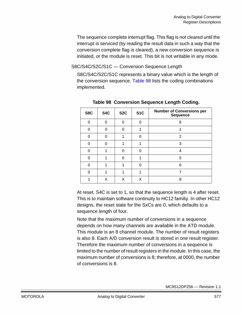
Analog to Digital ConverterRegister Descriptions
MC9S12DP256 — Revision 1.1
MOTOROLA Analog to Digital Converter 577
The sequence complete interrupt flag. This flag is not cleared until the interrupt is serviced (by reading the result data in such a way that the conversion complete flag is cleared), a new conversion sequence is initiated, or the module is reset. This bit is not writable in any mode.
S8C/S4C/S2C/S1C — Conversion Sequence Length
S8C/S4C/S2C/S1C represents a binary value which is the length of the conversion sequence. Table 98 lists the coding combinations implemented.
At reset, S4C is set to 1, so that the sequence length is 4 after reset. This is to maintain software continuity to HC12 familiy. In other HC12 designs, the reset state for the SxCs are 0, which defaults to a sequence length of four.
Note that the maximum number of conversions in a sequence depends on how many channels are available in the ATD module. This module is an 8 channel module. The number of result registers is also 8. Each A/D conversion result is stored in one result register. Therefore the maximum number of conversions in a sequence is limited to the number of result registers in the module. In this case, the maximum number of conversions is 8; therefore, at 0000, the number of conversions is 8.
Table 98 Conversion Sequence Length Coding.
S8C S4C S2C S1C Number of Conversions per Sequence
0 0 0 0 8
0 0 0 1 1
0 0 1 0 2
0 0 1 1 3
0 1 0 0 4
0 1 0 1 5
0 1 1 0 6
0 1 1 1 7
1 X X X 8
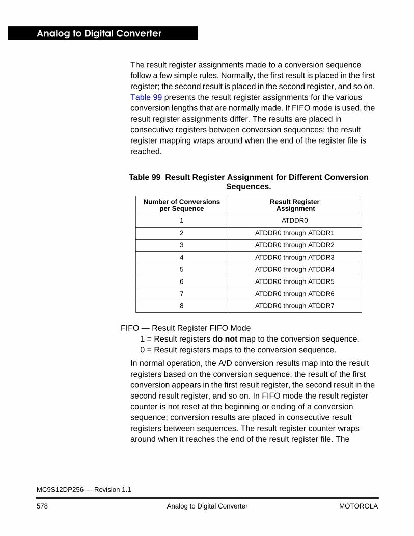
Analog to Digital Converter
MC9S12DP256 — Revision 1.1
578 Analog to Digital Converter MOTOROLA
The result register assignments made to a conversion sequence follow a few simple rules. Normally, the first result is placed in the first register; the second result is placed in the second register, and so on. Table 99 presents the result register assignments for the various conversion lengths that are normally made. If FIFO mode is used, the result register assignments differ. The results are placed in consecutive registers between conversion sequences; the result register mapping wraps around when the end of the register file is reached.
FIFO — Result Register FIFO Mode1 = Result registers do not map to the conversion sequence.0 = Result registers maps to the conversion sequence.
In normal operation, the A/D conversion results map into the result registers based on the conversion sequence; the result of the first conversion appears in the first result register, the second result in the second result register, and so on. In FIFO mode the result register counter is not reset at the beginning or ending of a conversion sequence; conversion results are placed in consecutive result registers between sequences. The result register counter wraps around when it reaches the end of the result register file. The
Table 99 Result Register Assignment for Different Conversion Sequences.
Number of Conversionsper Sequence
Result Register Assignment
1 ATDDR0
2 ATDDR0 through ATDDR1
3 ATDDR0 through ATDDR2
4 ATDDR0 through ATDDR3
5 ATDDR0 through ATDDR4
6 ATDDR0 through ATDDR5
7 ATDDR0 through ATDDR6
8 ATDDR0 through ATDDR7
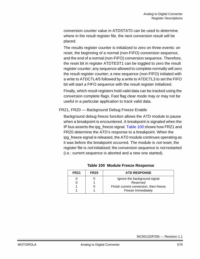
Analog to Digital ConverterRegister Descriptions
MC9S12DP256 — Revision 1.1
MOTOROLA Analog to Digital Converter 579
conversion counter value in ATDSTAT0 can be used to determine where in the result register file, the next conversion result will be placed.
The results register counter is initialized to zero on three events: on reset, the beginning of a normal (non-FIFO) conversion sequence, and the end of a normal (non-FIFO) conversion sequence. Therefore, the reset bit in register ATDTEST1 can be toggled to zero the result register counter; any sequence allowed to complete normally will zero the result register counter; a new sequence (non-FIFO) initiated with a write to ATDCTL4/5 followed by a write to ATDCTL3 to set the FIFO bit will start a FIFO sequence with the result register initialized.
Finally, which result registers hold valid data can be tracked using the conversion complete flags. Fast flag clear mode may or may not be useful in a particular application to track valid data.
FRZ1, FRZ0 — Background Debug Freeze Enable
Background debug freeze function allows the ATD module to pause when a breakpoint is encountered. A breakpoint is signaled when the IP bus asserts the ipg_freeze signal. Table 100 shows how FRZ1 and FRZ0 determine the ATD’s response to a breakpoint. When the ipg_freeze signal is released, the ATD module continues operating as it was before the breakpoint occurred. The module is not reset; the register file is not initialized; the conversion sequence is not restarted (i.e.: current sequence is aborted and a new one started).
Table 100 Module Freeze Response
FRZ1 FRZ0 ATD RESPONSE
0011
0101
Ignore the background signalReserved
Finish current conversion, then freezeFreeze Immediately

Analog to Digital Converter
MC9S12DP256 — Revision 1.1
580 Analog to Digital Converter MOTOROLA
ATD Control Register 4 (ATDCTL4)
ATD control register 4 is used to select the ATD conversion clock frequency (based on the ATD module clock), select the length of the third phase of the sample period, and set the resolution of the A/D conversion (i.e.: 8-bits or 10-bits). All writes to this register have an immediate effect. If a conversion is in progress, the entire conversion sequence is aborted.
SRES8 — A/D Resolution Select1 = 8-bit resolution selected.0 = 10-bit resolution selected.
This bit determines the resolution of the A/D converter: 8-bits or 10-bits. The A/D converter has the accuracy of a 10-bit converter. However, if low resolution is required, the conversion can be speeded up by selecting 8-bit resolution.
SMP0, SMP1 — Sample Time Select
These two bits select the length of the third phase of the sample period in ATD conversion clock cycles. Note that the ATD conversion clock period is itself a function of the prescaler value (bits PRS0-4). The sample period consists of three phases. The first phase is two ATD conversion clock cycles long and samples the signal on the channel’s sample capacitor. The second phase is four clock cycles and its purpose is to quickly transfer the sample onto the A/D machine’s storage node in preparation for conversion. The third phase occurs after the buffered sample and transfer and attaches the
Address Offset: $0004
Bit 15 14 13 12 11 10 9 Bit 8
SRES8 SMP1 SMP0 PRS4 PRS3 PRS2 PRS1 PRS0
Reset: 0 0 0 0 0 1 0 1
Analog to Digital ConverterRegister Descriptions
MC9S12DP256 — Revision 1.1
MOTOROLA Analog to Digital Converter 581
external analog signal directly to the storage node for final charging and high accuracy. Table 101 lists the lengths available for the third sample phase.
PRS0, PRS1, PRS2, PRS3, PRS4 — ATD Clock Prescaler
The binary prescaler value (0 to 31) plus one (1 to 32) becomes the divide-by factor for a modulus counter used to prescale the ATD module clock frequency. The resulting scaled clock is further divided by 2 before the ATD conversion clock is generated. This clock is used to drive the S/H and A/D machines.
Note that the maximum ATD conversion clock frequency is half of the ATD module clock. The default prescaler value is one which results in a default ATD conversion clock frequency that is quarter of the ATD module clock. Table 102 illustrates the divide-by operation and the appropriate range of ATD module clock frequencies.
Table 101 Sample Time Select
SMP1 SMP0 Final Sample Time
0011
0101
2 A/D clock periods4 A/D clock periods8 A/D clock periods16 A/D clock periods
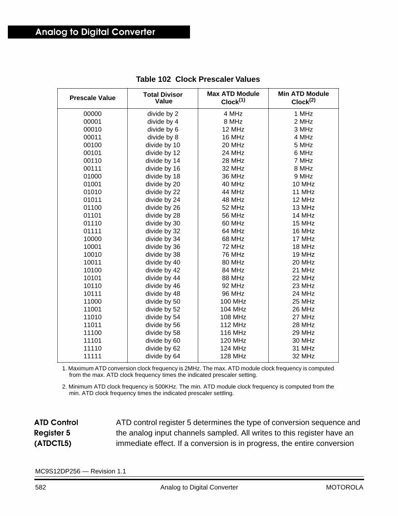
Analog to Digital Converter
MC9S12DP256 — Revision 1.1
582 Analog to Digital Converter MOTOROLA
ATD Control Register 5 (ATDCTL5)
ATD control register 5 determines the type of conversion sequence and the analog input channels sampled. All writes to this register have an immediate effect. If a conversion is in progress, the entire conversion
Table 102 Clock Prescaler Values
Prescale Value Total Divisor Value
Max ATD Module Clock(1)
Min ATD Module Clock(2)
0000000001000100001100100001010011000111010000100101010010110110001101011100111110000100011001010011101001010110110101111100011001110101101111100111011111011111
divide by 2divide by 4divide by 6divide by 8divide by 10divide by 12divide by 14divide by 16divide by 18divide by 20divide by 22divide by 24divide by 26divide by 28divide by 30divide by 32divide by 34divide by 36divide by 38divide by 40divide by 42divide by 44divide by 46divide by 48divide by 50divide by 52divide by 54divide by 56divide by 58divide by 60divide by 62divide by 64
4 MHz8 MHz12 MHz16 MHz20 MHz24 MHz28 MHz32 MHz36 MHz40 MHz44 MHz48 MHz52 MHz56 MHz60 MHz64 MHz68 MHz72 MHz76 MHz80 MHz84 MHz88 MHz92 MHz96 MHz100 MHz104 MHz108 MHz112 MHz116 MHz120 MHz124 MHz128 MHz
1 MHz2 MHz3 MHz4 MHz5 MHz6 MHz7 MHz8 MHz9 MHz10 MHz11 MHz12 MHz13 MHz14 MHz15 MHz16 MHz17 MHz18 MHz19 MHz20 MHz21 MHz22 MHz23 MHz24 MHz25 MHz26 MHz27 MHz28 MHz29 MHz30 MHz31 MHz32 MHz
1. Maximum ATD conversion clock frequency is 2MHz. The max. ATD module clock frequency is computedfrom the max. ATD clock frequency times the indicated prescaler setting.
2. Minimum ATD clock frequency is 500KHz. The min. ATD module clock frequency is computed from themin. ATD clock frequency times the indicated prescaler settling.
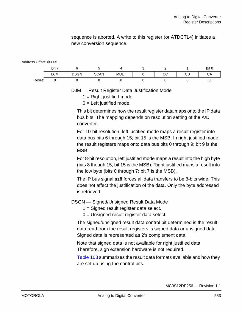
Analog to Digital ConverterRegister Descriptions
MC9S12DP256 — Revision 1.1
MOTOROLA Analog to Digital Converter 583
sequence is aborted. A write to this register (or ATDCTL4) initiates a new conversion sequence.
DJM — Result Register Data Justification Mode1 = Right justified mode.0 = Left justified mode.
This bit determines how the result register data maps onto the IP data bus bits. The mapping depends on resolution setting of the A/D converter.
For 10-bit resolution, left justified mode maps a result register into data bus bits 6 through 15; bit 15 is the MSB. In right justified mode, the result registers maps onto data bus bits 0 through 9; bit 9 is the MSB.
For 8-bit resolution, left justified mode maps a result into the high byte (bits 8 though 15; bit 15 is the MSB). Right justified maps a result into the low byte (bits 0 through 7; bit 7 is the MSB).
The IP bus signal sz8 forces all data transfers to be 8-bits wide. This does not affect the justification of the data. Only the byte addressed is retrieved.
DSGN — Signed/Unsigned Result Data Mode1 = Signed result register data select.0 = Unsigned result register data select.
The signed/unsigned result data control bit determined is the result data read from the result registers is signed data or unsigned data. Signed data is represented as 2’s complement data.
Note that signed data is not available for right justified data. Therefore, sign extension hardware is not required.
Table 103 summarizes the result data formats available and how they are set up using the control bits.
Address Offset: $0005
Bit 7 6 5 4 3 2 1 Bit 0
DJM DSGN SCAN MULT 0 CC CB CA
Reset: 0 0 0 0 0 0 0 0

Analog to Digital Converter
MC9S12DP256 — Revision 1.1
584 Analog to Digital Converter MOTOROLA
Table 104 illustrates the difference between the signed and unsigned, left justified output codes for an input signal range between 0 and 5.1 Volts.
SCAN — Continuous Conversion Sequence Mode1 = Perform conversion sequences continuously.0 = Perform a conversion sequence and return to idle mode.
The scan mode bit controls whether or not conversion sequences are performed continuously or not. If this control bit is 0, a write to control register 4 or 5 will initiate a conversion sequence; the conversion sequence will be executed; sequence complete flag (SCF) will be set, and the module will return to idle mode. In this mode, the module remains powered up but no conversions are performed; the module waits for the next conversion sequence to be initiated.
Table 103 Result Data Formats Available.
SRES8 DJM DSGN Result Data FormatsDescription and Bus Bit Mapping
111000
001001
01X01X
8-bit/left justified/unsigned - bits 8-158-bit/ left justified/signed - bits 8-15
8-bit/right justified/unsigned - bits 0-710-bit/left justified/unsigned - bits 6-1510-bit/left justified/signed - bits 6-15
10-bit/right justified/unsigned - bits 0-9
Table 104 Left Justified, Signed and Unsigned ATD Output Codes.
Input SignalVrl = 0 Volts
Vrh = 5.12 Volts
Signed8-Bit
Codes
Unsigned8-Bit
Codes
Signed10-BitCodes
Unsigned10-BitCodes
5.120 Volts5.1005.080
2.5802.5602.540
0.0200.000
7F7F7E
0100FF
8180
FFFFFE
81807F
0100
7FC07F007E00
01000000FF00
81008000
FFC0FF00FE00
810080007F00
01000000
Analog to Digital ConverterRegister Descriptions
MC9S12DP256 — Revision 1.1
MOTOROLA Analog to Digital Converter 585
If this control bit is 1, a single conversion sequence initiation will result in continuously executed conversion sequence. When a conversion sequence completes, the sequence complete flag (SCF) is set and a new sequence is immediately begun. The conversion mode characteristics of each sequence are identical. If a new conversion mode is required, the existing continuous sequence must be interrupted, the control registers modified, and a new conversion sequence initiated.
MULT — Multi-Channel Sample Mode1 = Sample across many channels.0 = Sample only the specified channel.
When MULT is 0, the ATD sequence controller samples only from the specified analog input channel for an entire conversion sequence. The analog channel is selected by channel selection code (control bits CC/CB/CA located in ATDCTL5). When MULT is 1, the ATD sequence controller samples across channels. The number of channels sampled is determined by the sequence length value (S8C, S1C control bits). The first analog channel examined is determined by channel selection code (CC, CB, CA control bits); subsequent channels sampled in the sequence are determined by incrementing the channel selection code.
CC, CB, CA — Analog Input Channel Select Code
These bits select the analog input channel(s) whose signals are sampled and converted to digital codes. Table 105 lists the coding used to select the various analog input channels. In the case of single channel scans (MULT=0), this selection code specified the channel examined. In the case of multi-channel scans (MULT=1), this selection code represents the first channel to be examined in the conversion sequence. Subsequent channels are determined by incrementing channel selection code; selection codes that reach the maximum value wrap around to the minimum value.
Note that for special conversion mode, bits CC/CB/CA have a different function. Instead of specifying the analog input channel, they identify which special channel conversion is to take place. See Table 106 for a list of the special conversions that are available through these bits.
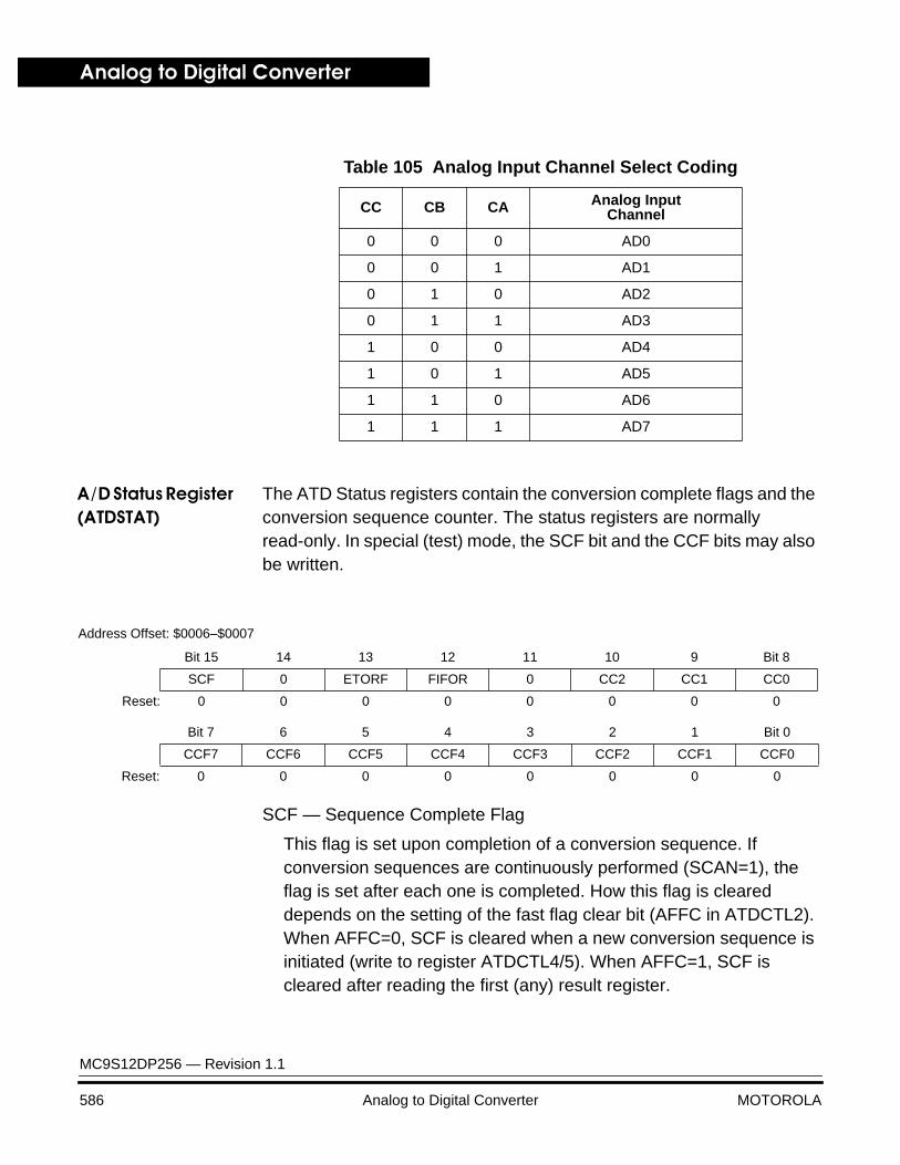
Analog to Digital Converter
MC9S12DP256 — Revision 1.1
586 Analog to Digital Converter MOTOROLA
A/D Status Register (ATDSTAT)
The ATD Status registers contain the conversion complete flags and the conversion sequence counter. The status registers are normally read-only. In special (test) mode, the SCF bit and the CCF bits may also be written.
SCF — Sequence Complete Flag
This flag is set upon completion of a conversion sequence. If conversion sequences are continuously performed (SCAN=1), the flag is set after each one is completed. How this flag is cleared depends on the setting of the fast flag clear bit (AFFC in ATDCTL2). When AFFC=0, SCF is cleared when a new conversion sequence is initiated (write to register ATDCTL4/5). When AFFC=1, SCF is cleared after reading the first (any) result register.
Table 105 Analog Input Channel Select Coding
CC CB CA Analog InputChannel
0 0 0 AD0
0 0 1 AD1
0 1 0 AD2
0 1 1 AD3
1 0 0 AD4
1 0 1 AD5
1 1 0 AD6
1 1 1 AD7
Address Offset: $0006–$0007
Bit 15 14 13 12 11 10 9 Bit 8
SCF 0 ETORF FIFOR 0 CC2 CC1 CC0
Reset: 0 0 0 0 0 0 0 0
Bit 7 6 5 4 3 2 1 Bit 0
CCF7 CCF6 CCF5 CCF4 CCF3 CCF2 CCF1 CCF0
Reset: 0 0 0 0 0 0 0 0
Analog to Digital ConverterRegister Descriptions
MC9S12DP256 — Revision 1.1
MOTOROLA Analog to Digital Converter 587
ETORF — External Trigger Overrun Flag
While in edge trigger mode, if additional active edges are detected while a conversion sequence is in process the overrun flag is set.
1 = External trigger overrun error has occurred0 = No External trigger overrun error has occurred
FIFOR — FIFO Over Run Flag.1 = An over run condition exists0 = No over run has occurred
This bit indicates that a result register has been written to before its associated conversion complete flag (CCF) has been cleared. This flag is most useful when using the FIFO mode because the flag potentially indicates that result registers are out of sync with the input channels. However, it is also practical for non-FIFO modes, and indicates that a result register has been over written before it has been read (i.e. the old data has been lost).
CC2/CC1/CC0 — Conversion Counter
This 3-bit value represents the contents of the result register counter; the result register counter points to the result register that will receive the result of the current conversion. If not in FIFO mode, the register counter is initialized to zero when a new conversion sequence is begun. If in FIFO mode, the register counter is not initialized. The result register count wraps around when its maximum value is reached.
CCF7 through CCF0 — Conversion Complete Flags
A conversion complete flag is set at the end of each conversion in a conversion sequence. The flags are associated with the conversion position in a sequence (and also the result register number). Therefore, CCF0 is set when the first conversion in a sequence is complete and the result is available in result register ATDDR0; CCF1 is set when the second conversion in a sequence is complete and the result is available in ATDDR1, and so forth.
The conversion complete flags are cleared depending on the setting of the fast flag clear bit (AFFC in ATDCTL2). When AFFC=0, the status register containing the conversion complete flag must be read as a precondition before the flag can be cleared. The flag is actually

Analog to Digital Converter
MC9S12DP256 — Revision 1.1
588 Analog to Digital Converter MOTOROLA
cleared during a subsequent access to the result register. This provides a convenient method for clearing the conversion complete flag when the user is polling the ATD module; it ensures the user is signaled as to the availability of new data and avoids having to have the user clear the flag explicitly.
When AFFC=1, the conversion complete flags are cleared when their associated result registers are read; reading the status register is not a necessary condition in order to clear them. This is the easiest method for clearing the conversion complete flags which is useful when the ATD module signals conversion completion with interrupt signals.
The conversion complete flags are normally read only; in special (test) mode they can be written. Note for writing ATDCTL4/5 registers.
When ATDCTL4/5 register is written, the SCF flags and all CCFx flags are cleared; any pending interrupt request is canceled.
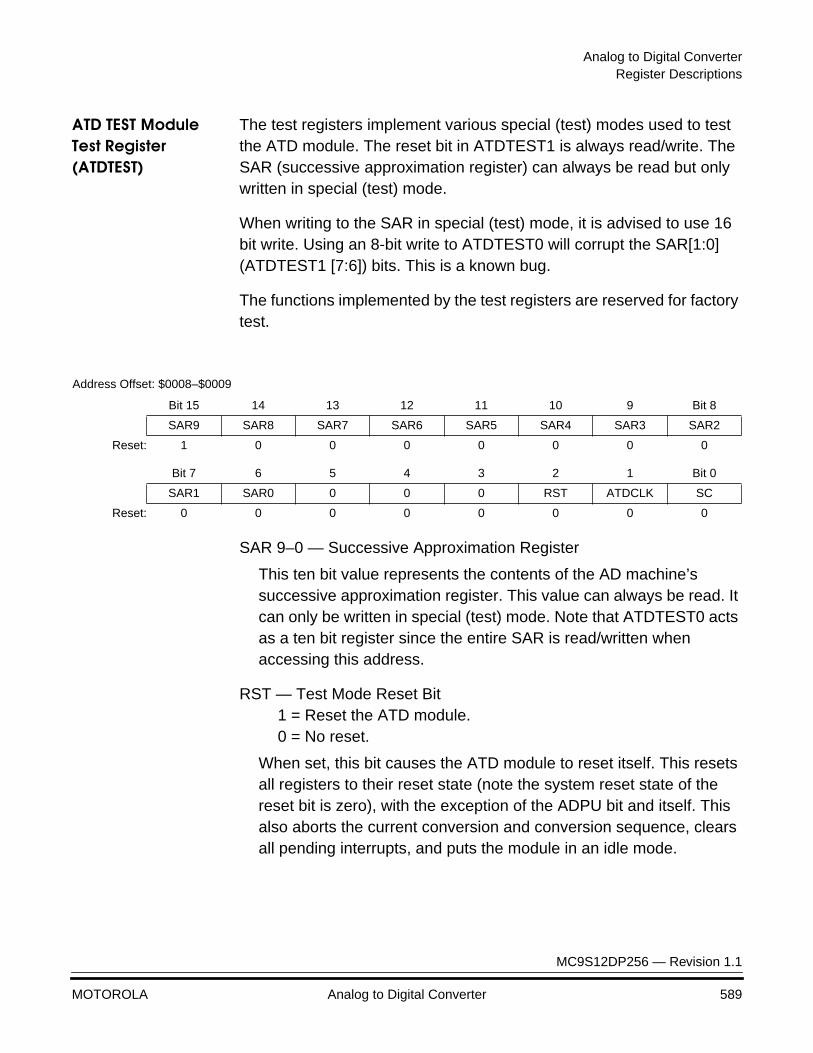
Analog to Digital ConverterRegister Descriptions
MC9S12DP256 — Revision 1.1
MOTOROLA Analog to Digital Converter 589
ATD TEST Module Test Register (ATDTEST)
The test registers implement various special (test) modes used to test the ATD module. The reset bit in ATDTEST1 is always read/write. The SAR (successive approximation register) can always be read but only written in special (test) mode.
When writing to the SAR in special (test) mode, it is advised to use 16 bit write. Using an 8-bit write to ATDTEST0 will corrupt the SAR[1:0] (ATDTEST1 [7:6]) bits. This is a known bug.
The functions implemented by the test registers are reserved for factory test.
SAR 9–0 — Successive Approximation Register
This ten bit value represents the contents of the AD machine’s successive approximation register. This value can always be read. It can only be written in special (test) mode. Note that ATDTEST0 acts as a ten bit register since the entire SAR is read/written when accessing this address.
RST — Test Mode Reset Bit1 = Reset the ATD module.0 = No reset.
When set, this bit causes the ATD module to reset itself. This resets all registers to their reset state (note the system reset state of the reset bit is zero), with the exception of the ADPU bit and itself. This also aborts the current conversion and conversion sequence, clears all pending interrupts, and puts the module in an idle mode.
Address Offset: $0008–$0009
Bit 15 14 13 12 11 10 9 Bit 8
SAR9 SAR8 SAR7 SAR6 SAR5 SAR4 SAR3 SAR2
Reset: 1 0 0 0 0 0 0 0
Bit 7 6 5 4 3 2 1 Bit 0
SAR1 SAR0 0 0 0 RST ATDCLK SC
Reset: 0 0 0 0 0 0 0 0
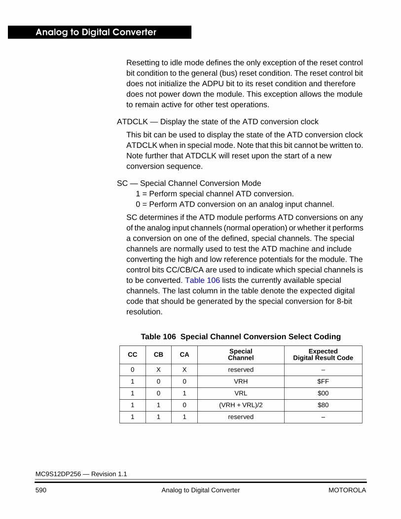
Analog to Digital Converter
MC9S12DP256 — Revision 1.1
590 Analog to Digital Converter MOTOROLA
Resetting to idle mode defines the only exception of the reset control bit condition to the general (bus) reset condition. The reset control bit does not initialize the ADPU bit to its reset condition and therefore does not power down the module. This exception allows the module to remain active for other test operations.
ATDCLK — Display the state of the ATD conversion clock
This bit can be used to display the state of the ATD conversion clock ATDCLK when in special mode. Note that this bit cannot be written to. Note further that ATDCLK will reset upon the start of a new conversion sequence.
SC — Special Channel Conversion Mode1 = Perform special channel ATD conversion.0 = Perform ATD conversion on an analog input channel.
SC determines if the ATD module performs ATD conversions on any of the analog input channels (normal operation) or whether it performs a conversion on one of the defined, special channels. The special channels are normally used to test the ATD machine and include converting the high and low reference potentials for the module. The control bits CC/CB/CA are used to indicate which special channels is to be converted. Table 106 lists the currently available special channels. The last column in the table denote the expected digital code that should be generated by the special conversion for 8-bit resolution.
Table 106 Special Channel Conversion Select Coding
CC CB CA SpecialChannel
Expected Digital Result Code
0 X X reserved –
1 0 0 VRH $FF
1 0 1 VRL $00
1 1 0 (VRH + VRL)/2 $80
1 1 1 reserved –
Analog to Digital ConverterRegister Descriptions
MC9S12DP256 — Revision 1.1
MOTOROLA Analog to Digital Converter 591
ATD Input Enable Mask Register (ATDDIEN)
This register is added for controlling the PORTAD1. Each bit individually enables the corresponding digital input buffers of PORTAD1
1 = Enable digital input buffer0 = Disable digital input buffer
This enable register confers the user greater control over the use of the ports. Note that when ATDDIEN enable bit is set, it will enable the input buffers continuously. The user is advised that if this bit is set while simultaneously using it as an analog port, the input buffer maybe in the linear region and therefore it may consume excessive power.
If the ATDDIEN bit is clear, a port read will return a “1”.
If the buffers are enabled during conversion, it will burn more power. The recommendation is to have buffers disabled during conversion. Due to internal synchronization circuits it can take up yo 2 bus cycles until the correct value is read on the PORTAD1 register.
Address Offset: $000D
Bit 7 6 5 4 3 2 1 Bit 0
Bit 7 Bit 6 Bit 5 Bit 4 Bit 3 Bit 2 Bit 1 Bit 0
Reset: 0 0 0 0 0 0 0 0

Analog to Digital Converter
MC9S12DP256 — Revision 1.1
592 Analog to Digital Converter MOTOROLA
Port Data Register (PORTAD1)
The input data port associated with the ATD module is input-only. The port pins are shared with the analog A/D inputs.
Reset: Reading this register out of reset will result in a “1” unless the pin was enabled by setting the respective bit in the ATDDIEN register, which is cleared out of reset.
The ATD input ports may be used for general purpose digital input. When the port data registers are read, they contain the digital levels appearing on the input pins at the time of the read. Input pins with signal potentials not meeting VIL or VIH specifications will have an indeterminate value.
Use of any Port pin for digital input does not preclude the use of any other Port pin for analog input. Note that the digital/analog multiplexing function is performed in the input pad. The port registers are connected to the input pads through a tristate buffers. These buffers are only activated when a read to a port register is performed so that analog signal potentials on the input pins will not cause the buffers to draw excess supply current.
Writes to this register have no meaning at any time.
Address Offset: $000F
Bit 7 6 5 4 3 2 1 Bit 0
Bit 7 Bit 6 Bit 5 Bit 4 Bit 3 Bit 2 Bit 1 Bit 0
Pin Function AN7 AN6 AN5 AN4 AN3 AN2 AN1 AN0
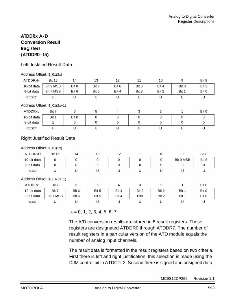
Analog to Digital ConverterRegister Descriptions
MC9S12DP256 — Revision 1.1
MOTOROLA Analog to Digital Converter 593
ATDDRx A/D Conversion Result Registers (ATDDR0Ð15)
Left Justified Result Data
Right Justified Result Data
x = 0, 1, 2, 3, 4, 5, 6, 7
The A/D conversion results are stored in 8 result registers. These registers are designated ATDDR0 through ATDDR7. The number of result registers in a particular version of the ATD module equals the number of analog input channels.
The result data is formatted in the result registers based on two criteria. First there is left and right justification; this selection is made using the DJM control bit in ATDCTL2. Second there is signed and unsigned data;
Address Offset: $_01(2x)
ATDDRxH Bit 15 14 13 12 11 10 9 Bit 8
10-bit data
8-bit data
Bit 9 MSB
Bit 7 MSB
Bit 8
Bit 6
Bit 7
Bit 5
Bit 6
Bit 4
Bit 5
Bit 3
Bit 4
Bit 2
Bit 3
Bit 1
Bit 2
Bit 0
RESET U U U U U U U U
Address Offset: $_01(2x+1)
ATDDRxL Bit 7 6 5 4 3 2 1 Bit 0
10-bit data
8-bit data
Bit 1
1
Bit 0
0
0
0
0
0
0
0
0
0
0
0
0
0
RESET U U U U U U U U
Address Offset: $_01(2x)
ATDDRxH Bit 15 14 13 12 11 10 9 Bit 8
10-bit data
8-bit data
0
0
0
0
0
0
0
0
0
0
0
0
Bit 9 MSB
0
Bit 8
0
RESET U U U U U U U U
Address Offset: $_01(2x+1)
ATDDRxL Bit 7 6 5 4 3 2 1 Bit 0
10-bit data
8-bit data
Bit 7
Bit 7 MSB
Bit 6
Bit 6
Bit 5
Bit 5
Bit 4
Bit 4
Bit 3
Bit3
Bit 2
Bit 2
Bit 1
Bit 1
Bit 0
Bit 0
RESET U U U U U U U U

Analog to Digital Converter
MC9S12DP256 — Revision 1.1
594 Analog to Digital Converter MOTOROLA
this selection is made using the DSGN control bit in ATDCTL2. Note that the signed data is stored in 2s complement format. Note that signed data only exists in left justified format so that no sign extension hardware is required. Signed data selected for right justified format is ignored.
For 8-bit result data, the result data maps between the high (left justified) and low (right justified) order bytes of the result register. For 10-bit result data, the result data maps between bits 6–15 (left justified) and bits 0–9 (right justified) of the result register. Therefore for each bit in the SAR, there are 3 possible mappings of this bit into the result registers.
These registers are normally read-only. In special (test) mode the result registers can be written.
Analog to Digital ConverterExternal Pin Descriptions
MC9S12DP256 — Revision 1.1
MOTOROLA Analog to Digital Converter 595
External Pin Descriptions
The basic ATD requires a total of 12 pins to implement the 8 input channel A/D converter. The pins fall into four categories: channel input pins (one of the channel input pins is muxed with the ETRIG input), reference potential pins (VRL and VRH), and analog supply potential pins (VDDA and VSSA). These pins are described below.
Channel Pins The 8 channel pins serve three purposes.
First, the channel pins are used as the analog input pins of the ATD. Each pin is connected to an analog switch which serves as the signal gate into the sample submodule.
Second, the channel pins can also be used to collect general purpose digital input data. The digital data must meet the VIH and VIL specifications. The channel pins are also connected to the input of a Schmitt Trigger which drives the digital data to the Port Data Register (PORTAD1). The Schmitt Trigger is disabled when the respective ATDDIEN bit is set to “0”. The digital input data is accessed via the PORTAD1 Registers. Since the port PORTAD1 pins are used only as inputs in normal operating modes, no data direction register is necessary for this port.
Third, channel 7 pin is used to provide the external trigger signal to the module. The ATDDIEN bit 7 must be set to enable schmitt trigger input buffer.
External Trigger Input Pin (ETRIG)
As a module variability, the ETRIG pin may occupy a separate pin, or the channel 7 pin may be used to provide the external trigger input signal when the external trigger mode is enabled.External trigger mode is enabled using the control bits in the ATDCTL2 register. Triggering is synchronized to the ATD module clock; when a active falling or rising edge on the trigger signal or the correct level is detected, a new conversion cycle begins.
Analog to Digital Converter
MC9S12DP256 — Revision 1.1
596 Analog to Digital Converter MOTOROLA
Analog Reference Pins
These two pins serve as the source for the high (VRH) and low (VRL) reference potentials for the converter.
Separation from the power supply pins accommodates the filtering necessary to achieve the accuracy of which the system is capable. Dedicated Analog Supply Pins
These two pins are used to supply power (VDDA and VSSA) to the analog section of the chip. Dedicated power is required to isolate the sensitive analog circuitry from the normal levels of noise present on the digital power supply.
Reset Initialization
The reset state of each individual bit is listed within the Register Description section (see Register Descriptions) which details the registers and their bit-fields. All special functions or modes which are initialized during or just following reset are described within this section.
Analog to Digital ConverterModes of Operation
MC9S12DP256 — Revision 1.1
MOTOROLA Analog to Digital Converter 597
Modes of Operation
Analog to digital conversions in this module are performed in sequences. There are a variety of different sequences that are programmable; these different sequences are referred to as conversion modes1. A particular conversion mode is defined by how many A/D conversions are performed in a sequence, which analog input channels are examined during a sequence, sample time length, whether sequences are performed continuously or not, what event is used to trigger a conversion, result register assignments, and so on.
The conversion modes for the ATD module are defined by the settings of four control bits and three control values. The control bits are ETRIGE in ATDCTL2 and MULT, SCAN and SC in ATDCTL5. In brief, ETRIGE controls whether an external trigger is used to start a conversion sequence. MULT controls whether the sequence examines a single analog input channel or scans a number of different channels. SCAN determines if sequences are performed continuously. SC determines if we are performing a special conversion (i.e.: convert Vrl, Vrh, (Vrl+Vrh)/2, usually used for test purposes). The control values are bits CC/CB/CA in ATDCTL3/5 which define the input channels to be examined; S8C/S1C in ATDCTL3/5 define the number of conversions in a sequence; SMP0/SMP1 in ATDCTL4 define the length of the sample time.
Sequences are initiated by writing to control registers 4 and 5. For the continuous sequence modes, conversions will not stop until either another non-continuous conversion sequence is initiated and finishes, the ATD is powered down (ADPU control bit), the ATD is reset (by the bus or the control bit), the bus ipg_wait line is activated (if the wait bit is activated), or the bus ipg_stop line is activated. Note that the ipg_wait signal suspends the current conversion until the ipg_wait is deactivated - it does not terminate the conversion. The result of suspended conversion is not guaranteed.
The MCU can use one of two methods to learn when the result data is available in the result registers. First, the interrupt enable bit can be used to interrupt the MCU when the sequence is complete. Second, the conversion complete flags can be used to poll the ATD module to
Analog to Digital Converter
MC9S12DP256 — Revision 1.1
598 Analog to Digital Converter MOTOROLA
determine when the result registers have been filled. The SCF bit is set after the completion of each sequence. The CCF bit associated with each result register is set when that register is loaded with result data.
1) Do not confuse conversion modes with MCU operating modes such as STOP, WAIT, IDLE, RUN, DEBUG, and SPECIAL (test) modes, and do not confuse with module defined operating modes such as power down, fast flag clear, 8-bit resolution, 10-bit resolution, interrupt enable, clock prescaler setting, and freeze modes, and finally do not confuse with module result data formats such as right justify mode, left justify mode, and signed/unsigned data.
Special Operation Special mode is a device test mode. Special mode is entered when the IP ipbi_test_mod signal is asserted. This mode allows increased access to the control, status, and test registers. A number of special mode test functions are also available.
Run Mode RUN mode for the ATD module is defined as the state where the ATD module is powered up and currently performing an A/D conversion. Complete assess to all control, status, and result registers is available. The module is consuming maximum power.
Wait Mode WAIT mode is a maskable form of power saving.
WAIT mode is signalled to the ATD by asserting the ipg_wait signal on the bus. If the AWAI control bit in ATDCTL2 is set, then the ATD responds to WAIT mode. If the AWAI control bit is clear, then the ATD ignores the ipg_wait signal. The ATD response to the wait mode is to power down the module. The module is released from WAIT mode when the ipg_wait signal is released.
In this mode, the MCU does not have access to the control, status, or result registers.
Stop Mode STOP mode is a global mode that can be used to place the entire device into power saving operation.
STOP mode is signalled to the ATD by asserting the ipg_stop signal. This causes the ATD module to power down the ATD module. The digital
Analog to Digital ConverterSample Conversion
MC9S12DP256 — Revision 1.1
MOTOROLA Analog to Digital Converter 599
clocks are disabled to most of the module and the analog quiescent current draw is turned off; this places the module into its power down state. This mode is equivalent to clearing the ADPU control bit in ATDCTL2. The module is released from STOP mode when the ipg_stop signal is released.
In this mode, the MCU still has access to the control, status, and result registers.
IDLE Mode IDLE mode for the ATD module is defined as the state where the ATD module is powered up and ready to perform an A/D conversion, but not actually performing a conversion at the present time. Complete assess to all control, status, and result registers is available. The module is consuming near maximum power.
Sample Conversion
The sample/conversion time has three components: the initial sample time, the final sample time, and resolution time. The initial sample time is fixed at 2 ATD clock cycles. The final sample time is programmable through control register ATDCTL 4 and can be 2, 4, 8, or 16 ATD clocks cycles long. For a 10-bit conversion, the resolution time is 10 ATD clock cycles.
Figure 112 illustrates how an ATD sample/conversion period is broken into its various components for an 10-bit conversion with a programmable sample time of 2 ATD clock cycles.
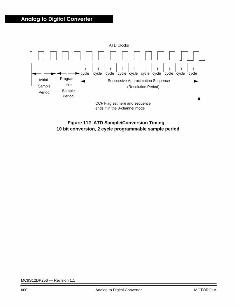
Analog to Digital Converter
MC9S12DP256 — Revision 1.1
600 Analog to Digital Converter MOTOROLA
Figure 112 ATD Sample/Conversion Timing –10 bit conversion, 2 cycle programmable sample period
1cycle
1cycle
1cycle
1cycle
1cycle
1cycle
1cycle
Successive Approximation Sequence
ATD Clocks
CCF Flag set here and sequenceends if in the 8-channel mode
Period
Program-
SamplePeriod
(Resolution Period)
1cycle
ableInitial
Sample
1cycle
1cycle
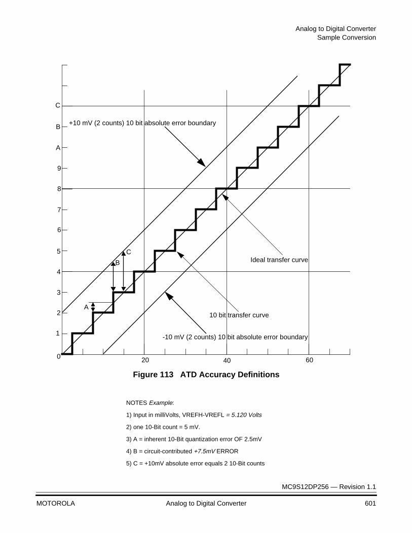
Analog to Digital ConverterSample Conversion
MC9S12DP256 — Revision 1.1
MOTOROLA Analog to Digital Converter 601
Figure 113 ATD Accuracy Definitions
NOTES Example:
1) Input in milliVolts, VREFH-VREFL = 5.120 Volts
2) one 10-Bit count = 5 mV.
3) A = inherent 10-Bit quantization error OF 2.5mV
4) B = circuit-contributed +7.5mV ERROR
5) C = +10mV absolute error equals 2 10-Bit counts
20 40 600
1
2
3
4
5
6
7
8
9
A
B
C
+10 mV (2 counts) 10 bit absolute error boundary
-10 mV (2 counts) 10 bit absolute error boundary
A
B
CIdeal transfer curve
10 bit transfer curve
Analog to Digital Converter
MC9S12DP256 — Revision 1.1
602 Analog to Digital Converter MOTOROLA
General Purpose Input Ports
The input channel pins can be multiplexed between analog and digital data. As analog inputs, they are multiplexed and sampled to supply signals to the A/D converter. As digital inputs, they supply external input data that can be accessed through the digital port registers. Each digital input is individually enabled by each bit of the register ATDDIEN.
The analog/digital multiplex operation is performed in the input pads. The input pad is always connected to the analog inputs of the ATD module. The input pad signal is buffered before the data is bussed to the digital port registers. The buffer is a schmitt trigger nand gate so that the buffer can be turned off. This is important so that the buffer does not draw excess current when analog potentials are presented at its input. This is particularly important when some of the inputs are being used as digital inputs and some as analog inputs. Analog signals present on the input pins at the digital sampling time that don’t meet the VIL or VIH specification will return unknown digital values. A read of the PORTAD1 may affect the accuracy of an in progress sample period but will not affect an in progress A/D conversion.
There is a digital, 8-bit, input-only port associated with the ATD. It is accessed through the 8-bit Port Data Registers (PORTAD1). The number of bits utilized in the port register depends on the number of analog channels implemented with the 8 channel ATD module.
MC9S12DP256 — Revision 1.1
MOTOROLA Byte Data Link Controller Module 603
Byte Data Link Controller ModuleByte Data Link Controller Module
Contents
Overview . . . . . . . . . . . . . . . . . . . . . . . . . . . . . . . . . . . . . . . . . . . . . . 603Features . . . . . . . . . . . . . . . . . . . . . . . . . . . . . . . . . . . . . . . . . . . . . . 604Block Diagram. . . . . . . . . . . . . . . . . . . . . . . . . . . . . . . . . . . . . . . . . . 605Register Map. . . . . . . . . . . . . . . . . . . . . . . . . . . . . . . . . . . . . . . . . . . 606Functional Description. . . . . . . . . . . . . . . . . . . . . . . . . . . . . . . . . . . . 607Register Descriptions . . . . . . . . . . . . . . . . . . . . . . . . . . . . . . . . . . . . 633External Pin Descriptions . . . . . . . . . . . . . . . . . . . . . . . . . . . . . . . . . 653Reset Initialization/Basic Operation . . . . . . . . . . . . . . . . . . . . . . . . . 653Transmitting A Message . . . . . . . . . . . . . . . . . . . . . . . . . . . . . . . . . . 658Receiving A Message . . . . . . . . . . . . . . . . . . . . . . . . . . . . . . . . . . . . 664Transmitting An In-Frame Response (IFR) . . . . . . . . . . . . . . . . . . . . 669Receiving An In-Frame Response (IFR) . . . . . . . . . . . . . . . . . . . . . . 681Special BDLC Operations . . . . . . . . . . . . . . . . . . . . . . . . . . . . . . . . . 683Modes of Operation. . . . . . . . . . . . . . . . . . . . . . . . . . . . . . . . . . . . . . 684Interrupt Operation . . . . . . . . . . . . . . . . . . . . . . . . . . . . . . . . . . . . . . 689Low Power Options . . . . . . . . . . . . . . . . . . . . . . . . . . . . . . . . . . . . . . 689
Overview
The BDLC module is a serial communication module which allows the user to send and receive messages across a Society of Automotive Engineers (SAE) J1850 serial communication network. The user’s software handles each transmitted or received message on a byte-by-byte basis, while the BDLC performs all of the network access, arbitration, message framing and error detection duties.
It is recommended that the reader be familiar with the operation and requirements of the SAE J1850 protocol as described in the document
Byte Data Link
MC9S12DP256 — Revision 1.1
604 Byte Data Link Controller Module MOTOROLA
“SAE Standard J1850 Class B Data Communications Network Interface” prior to proceeding with this specification.
The BDLC module is designed in a modular structure for use as an IP block.
Features
Features of the BDLC module include the following:
• SAE J1850 Class B Data Communications Network Interface Compatible and ISO Compatible for Low-Speed (≤125 Kbps) Serial Data Communications in Automotive Applications
• 10.4 Kbps Variable Pulse Width (VPW) Bit Format
• Digital Noise Filter
• Collision Detection
• Hardware Cyclical Redundancy Check (CRC) Generation and Checking
• Block Mode Receive and Transmit Supported
• 4X Receive Mode, 41.6 Kbps, Supported
• Digital Loopback Mode
• In-Frame Response (IFR) Types 0, 1, 2, and 3 Supported
• Dedicated Register for Symbol Timing Adjustments
• IP Bus Interface
• Power-Saving Stop and Wait Modes with Automatic Wakeup on Network Activity
• Polling and CPU Interrupt Generation with Vector Lookup Available
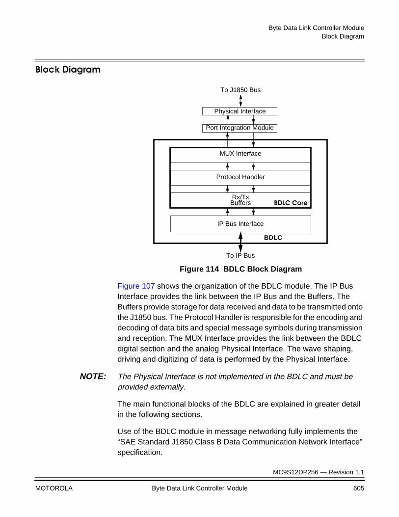
Byte Data Link Controller ModuleBlock Diagram
MC9S12DP256 — Revision 1.1
MOTOROLA Byte Data Link Controller Module 605
Block Diagram
Figure 114 BDLC Block Diagram
Figure 107 shows the organization of the BDLC module. The IP Bus Interface provides the link between the IP Bus and the Buffers. The Buffers provide storage for data received and data to be transmitted onto the J1850 bus. The Protocol Handler is responsible for the encoding and decoding of data bits and special message symbols during transmission and reception. The MUX Interface provides the link between the BDLC digital section and the analog Physical Interface. The wave shaping, driving and digitizing of data is performed by the Physical Interface.
NOTE: The Physical Interface is not implemented in the BDLC and must be provided externally.
The main functional blocks of the BDLC are explained in greater detail in the following sections.
Use of the BDLC module in message networking fully implements the “SAE Standard J1850 Class B Data Communication Network Interface” specification.
To IP Bus
Protocol Handler
MUX Interface
IP Bus Interface
Rx/TxBuffers
Physical Interface
To J1850 Bus
BDLC
Port Integration Module
BDLC Core
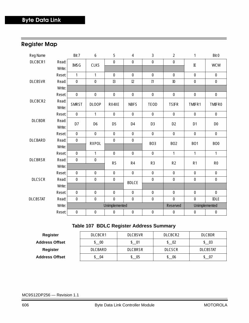
Byte Data Link
MC9S12DP256 — Revision 1.1
606 Byte Data Link Controller Module MOTOROLA
Register Map
Reg Name Bit 7 6 5 4 3 2 1 Bit 0
DLCBCR1 Read:IMSG CLKS
0 0 0 0IE WCM
Write:
Reset: 1 1 0 0 0 0 0 0
DLCBSVR Read: 0 0 I3 I2 I1 I0 0 0
Write:
Reset: 0 0 0 0 0 0 0 0
DLCBCR2 Read:SMRST DLOOP RX4XE NBFS TEOD TSIFR TMIFR1 TMIFR0
Write:
Reset: 0 1 0 0 0 0 0 0
DLCBDR Read:D7 D6 D5 D4 D3 D2 D1 D0
Write:
Reset: 0 0 0 0 0 0 0 0
DLCBARD Read: 0RXPOL
0 0BO3 BO2 BO1 BO0
Write:
Reset: 0 1 0 0 0 1 1 1
DLCBRSR Read: 0 0R5 R4 R3 R2 R1 R0
Write:
Reset: 0 0 0 0 0 0 0 0
DLCSCR Read: 0 0 0BDLCE
0 0 0 0
Write:
Reset: 0 0 0 0 0 0 0 0
DLCBSTAT Read: 0 0 0 0 0 0 0 IDLE
Write: Unimplemented Reserved Unimplemented
Reset: 0 0 0 0 0 0 0 0
Table 107 BDLC Register Address Summary
Register DLCBCR1 DLCBSVR DLCBCR2 DLCBDR
Address Offset $__00 $__01 $__02 $__03
Register DLCBARD DLCBRSR DLCSCR DLCBSTAT
Address Offset $__04 $__05 $__06 $__07
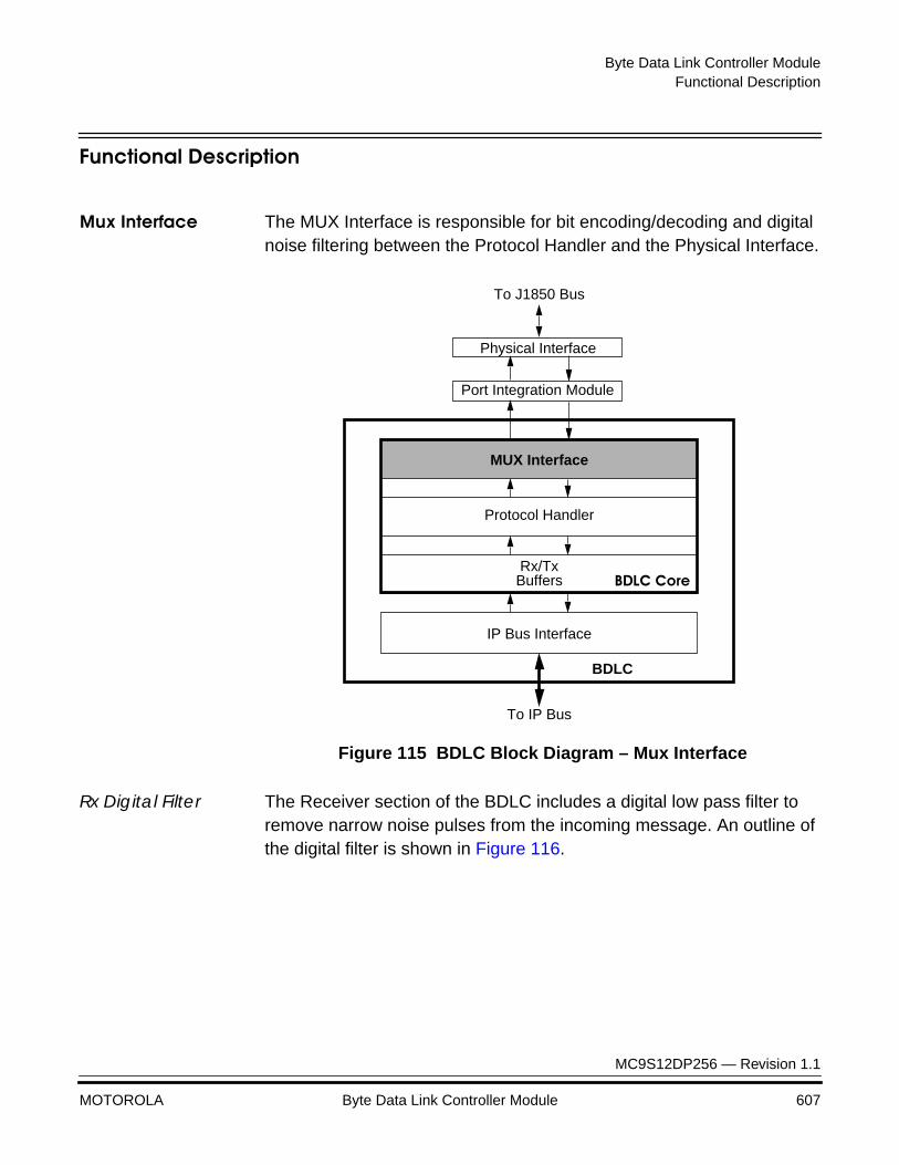
Byte Data Link Controller ModuleFunctional Description
MC9S12DP256 — Revision 1.1
MOTOROLA Byte Data Link Controller Module 607
Functional Description
Mux Interface The MUX Interface is responsible for bit encoding/decoding and digital noise filtering between the Protocol Handler and the Physical Interface.
Figure 115 BDLC Block Diagram – Mux Interface
Rx Digital Filter The Receiver section of the BDLC includes a digital low pass filter to remove narrow noise pulses from the incoming message. An outline of the digital filter is shown in Figure 116.
To IP Bus
Protocol Handler
MUX Interface
IP Bus Interface
Rx/TxBuffers
Physical Interface
To J1850 Bus
BDLC
Port Integration Module
BDLC Core
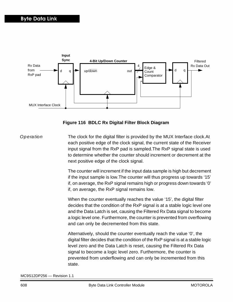
Byte Data Link
MC9S12DP256 — Revision 1.1
608 Byte Data Link Controller Module MOTOROLA
Figure 116 BDLC Rx Digital Filter Block Diagram
Operation The clock for the digital filter is provided by the MUX Interface clock.At each positive edge of the clock signal, the current state of the Receiver input signal from the RxP pad is sampled.The RxP signal state is used to determine whether the counter should increment or decrement at the next positive edge of the clock signal.
The counter will increment if the input data sample is high but decrement if the input sample is low.The counter will thus progress up towards ‘15’ if, on average, the RxP signal remains high or progress down towards ‘0’ if, on average, the RxP signal remains low.
When the counter eventually reaches the value ‘15’, the digital filter decides that the condition of the RxP signal is at a stable logic level one and the Data Latch is set, causing the Filtered Rx Data signal to become a logic level one. Furthermore, the counter is prevented from overflowing and can only be decremented from this state.
Alternatively, should the counter eventually reach the value ‘0’, the digital filter decides that the condition of the RxP signal is at a stable logic level zero and the Data Latch is reset, causing the Filtered Rx Data signal to become a logic level zero. Furthermore, the counter is prevented from underflowing and can only be incremented from this state.
4-Bit Up/Down Counter
up/down out d q
FilteredRx Data Out
MUX Interface Clock
InputSync
d q
Rx DatafromRxP pad
4Edge & CountComparator
Byte Data Link Controller ModuleFunctional Description
MC9S12DP256 — Revision 1.1
MOTOROLA Byte Data Link Controller Module 609
The Data Latch will retain its value until the counter next reaches the opposite end point, signifying a definite transition of the RxP signal.
Performance The performance of the digital filter is best described in the time domain rather than the frequency domain.
If the signal on the RxP signal transitions, then there will be a delay before that transition appears at the Filtered Rx Data output signal. This delay will be between 15 and 16 clock periods, depending on where the transition occurs with respect to the sampling points. This ‘filter delay’ must be taken into account when performing message arbitration.
For example, if the frequency of the MUX Interface clock (fbdlc) is 1.0486MHz, then the period (tbdlc) is 954ns and the maximum filter delay in the absence of noise will be 15.259us.
The effect of random noise on the RxP signal depends on the characteristics of the noise itself. Narrow noise pulses on the RxP signal will be completely ignored if they are shorter than the filter delay. This provides a degree of low pass filtering.
If noise occurs during a symbol transition, the detection of that transition may be delayed by an amount equal to the length of the noise burst. This is just a reflection of the uncertainty of where the transition is truly occurring within the noise.
Noise pulses that are wider than the filter delay, but narrower than the shortest allowable symbol length will be detected by the next stage of the BDLC’s receiver as an invalid symbol.
Noise pulses that are longer than the shortest allowable symbol length will normally be detected as an invalid symbol or as invalid data when the frame’s CRC is checked.
J1850 Frame Format
All messages transmitted on the J1850 bus are structured using the format:
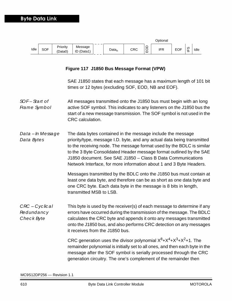
Byte Data Link
MC9S12DP256 — Revision 1.1
610 Byte Data Link Controller Module MOTOROLA
Figure 117 J1850 Bus Message Format (VPW)
SAE J1850 states that each message has a maximum length of 101 bit times or 12 bytes (excluding SOF, EOD, NB and EOF).
SOF – Start of Frame Symbol
All messages transmitted onto the J1850 bus must begin with an long active SOF symbol. This indicates to any listeners on the J1850 bus the start of a new message transmission. The SOF symbol is not used in the CRC calculation.
Data – In Message Data Bytes
The data bytes contained in the message include the message priority/type, message I.D. byte, and any actual data being transmitted to the receiving node. The message format used by the BDLC is similar to the 3 Byte Consolidated Header message format outlined by the SAE J1850 document. See SAE J1850 – Class B Data Communications Network Interface, for more information about 1 and 3 Byte Headers.
Messages transmitted by the BDLC onto the J1850 bus must contain at least one data byte, and therefore can be as short as one data byte and one CRC byte. Each data byte in the message is 8 bits in length, transmitted MSB to LSB.
CRC – Cyclical Redundancy Check Byte
This byte is used by the receiver(s) of each message to determine if any errors have occurred during the transmission of the message. The BDLC calculates the CRC byte and appends it onto any messages transmitted onto the J1850 bus, and also performs CRC detection on any messages it receives from the J1850 bus.
CRC generation uses the divisor polynomial X8+X4+X3+X2+1. The remainder polynomial is initially set to all ones, and then each byte in the message after the SOF symbol is serially processed through the CRC generation circuitry. The one’s complement of the remainder then
SOF
EO
D
EOFPriority Message
Datan CRC IFR IFSIdle IdleID (Data1)(Data0)
Optional

Byte Data Link Controller ModuleFunctional Description
MC9S12DP256 — Revision 1.1
MOTOROLA Byte Data Link Controller Module 611
becomes the 8-bit CRC byte, which is appended to the message after the data bytes, in MSB to LSB order.
When receiving a message, the BDLC uses the same divisor polynomial. All data bytes, excluding the SOF and EOD symbols, but including the CRC byte, are used to check the CRC. If the message is error free, the remainder polynomial will equal X7+X6+X2 ($C4), regardless of the data contained in the message. If the calculated CRC does not equal $C4, the BDLC will recognize this as a CRC error and set the CRC error flag in the BSVR register.
EOD – End of Data Symbol
The EOD symbol is a long passive period on the J1850 bus used to signify to any recipients of a message that the transmission by the originator has completed. No flag is set upon reception of EOD symbol.
IFR – In Frame Response Bytes
The IFR section of the J1850 message format is optional. Users desiring further definition of in-frame response should review the “SAE J1850 Class B Data Communications Network Interface” specification.
EOF – End of Frame Symbol
This symbol is a passive period on the J1850 bus, longer than an EOD symbol, which signifies the end of a message. Since an EOF symbol is longer than an EOD symbol, if no response is transmitted after an EOD symbol, it becomes an EOF, and the message is assumed to be completed.The EOF flag is set upon receiving the EOF symbol.
IFS – Inter-Frame Separation Symbol
The IFS symbol is a passive period on the J1850 bus which allows proper synchronization between nodes during continuous message transmission. The IFS symbol is transmitted by a node following the completion of the EOF period.
When the last byte of a message has been transmitted onto the J1850 bus, and the EOF symbol time has expired, all nodes must then wait for the IFS symbol time to expire before transmitting an SOF, marking the beginning of another message.
However, if the BDLC is waiting for the IFS period to expire before beginning a transmission and a rising edge is detected before the IFS time has expired, it will internally synchronize to that edge.
Byte Data Link
MC9S12DP256 — Revision 1.1
612 Byte Data Link Controller Module MOTOROLA
A rising edge may occur during the IFS period because of varying clock tolerances and loading of the J1850 bus, causing different nodes to observe the completion of the IFS period at different times. Receivers must synchronize to any SOF occurring during an IFS period to allow for individual clock tolerances.
Break If the BDLC is transmitting at the time a BREAK is detected, it treats the BREAK as if a transmission error had occurred, and halts transmission.The BDLC cannot transmit a BREAK symbol. If while receiving a message the BDLC detects a BREAK symbol, it treats the BREAK as a reception error and sets the invalid symbol flag.If while receiving a message in 4X mode, the BDLC detects a BREAK symbol, it treats the BREAK as a reception error, sets BSVR register to $1C, and exits 4X mode.The RX4XE bit in BCR2 is automatically cleared upon reception of the BREAK symbol.
Idle Bus An idle condition exists on the bus during any passive period after expiration of the IFS period. Any node sensing an idle bus condition can begin transmission immediately.
J1850 VPW Symbols
Variable Pulse Width modulation (VPW) is an encoding technique in which each bit is defined by the time between successive transitions, and by the level of the bus between transitions, active or passive. Active and passive bits are used alternately. This encoding technique is used to reduced the number of bus transitions for a given bit rate.
The symbol values shown below are nominal values. Refer to the electrical specification for a more complete description of symbol values. Each logic one or logic zero contains a single transition, and can be at either the active or passive level and one of two lengths, either 64µs or 128µs (TNOM at 10.4kbps baud rate), depending upon the encoding of the previous bit. The SOF, EOD, EOF and IFS symbols will always be encoded at an assigned level and length. See Figure 118.
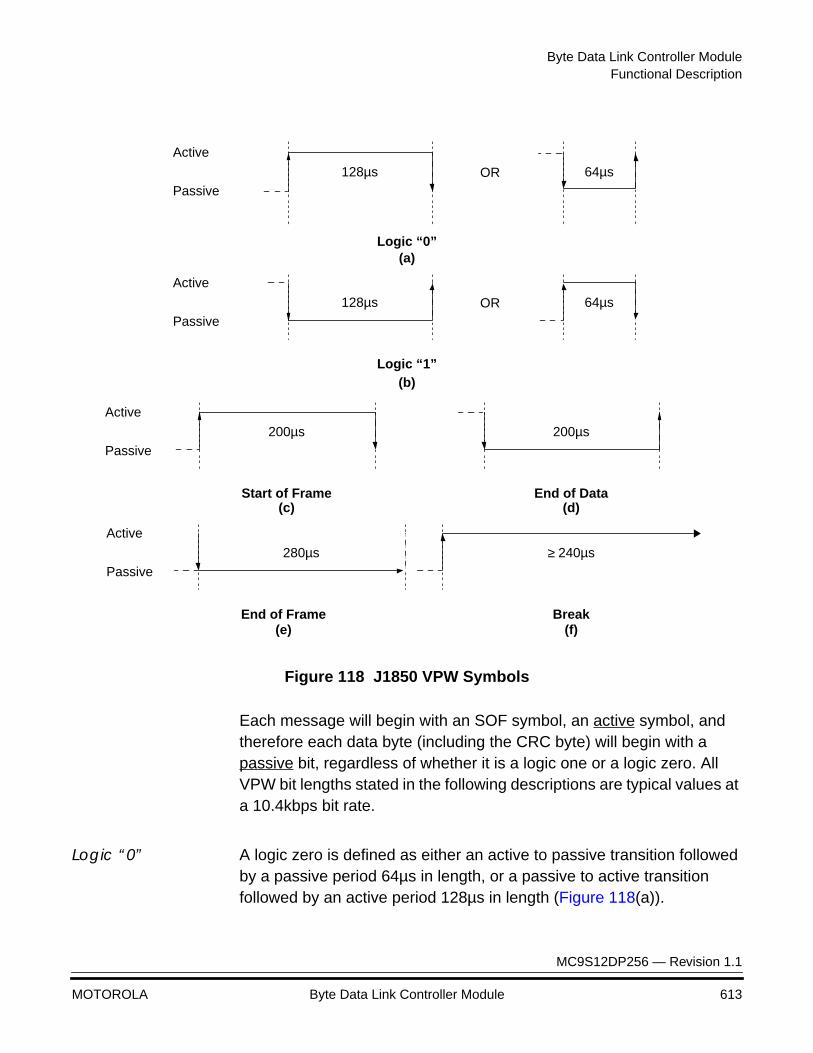
Byte Data Link Controller ModuleFunctional Description
MC9S12DP256 — Revision 1.1
MOTOROLA Byte Data Link Controller Module 613
Figure 118 J1850 VPW Symbols
Each message will begin with an SOF symbol, an active symbol, and therefore each data byte (including the CRC byte) will begin with a passive bit, regardless of whether it is a logic one or a logic zero. All VPW bit lengths stated in the following descriptions are typical values at a 10.4kbps bit rate.
Logic “0” A logic zero is defined as either an active to passive transition followed by a passive period 64µs in length, or a passive to active transition followed by an active period 128µs in length (Figure 118(a)).
128µs
Active
Passive64µsOR
Logic “0”
128µs
Active
Passive64µsOR
Logic “1”
200µs
Active
Passive
Start of Frame
200µs
End of Data
280µs
Active
Passive
End of Frame
≥ 240µs
Break
(a)
(b)
(c) (d)
(e) (f)

Byte Data Link
MC9S12DP256 — Revision 1.1
614 Byte Data Link Controller Module MOTOROLA
Logic “1” A logic one is defined as either an active to passive transition followed by a passive period 128µs in length, or a passive to active transition followed by an active period 64µs in length (Figure 118(b)).
NB – Normalization Bit
The NB symbol has the same property as a logic “1” or a logic “0”.It is only used in IFR message responses.
SOF -– Start of Frame Symbol
The SOF symbol is defined as passive to active transition followed by an active period 200µs in length (Figure 118(c)). This allows the data bytes which follow the SOF symbol to begin with a passive bit, regardless of whether it is a logic one or a logic zero.
EOD – End of Data Symbol
The EOD symbol is defined as an active to passive transition followed by a passive period 200µs in length (Figure 118(d)).
EOF – End of Frame Symbol
The EOF symbol is defined as an active to passive transition followed by a passive period 280µs in length (Figure 118(e)). If there is no IFR byte transmitted after an EOD symbol is transmitted, after another 80µs the EOD becomes an EOF, indicating the completion of the message.
IFS – Inter-Frame Separation Symbol
The IFS symbol is defined as a passive period 300µs in length. The IFS symbol contains no transition, since when used it always follows an EOF symbol.
BREAK – Break Signal
The BREAK signal is defined as a passive to active transition followed by an active period of at least 240µs (Figure 118(f)).
IDLE An IDLE is defined as a passive period greater than 300µs in length.
J1850 VPW Valid/Invalid Bits & Symbols
The timing tolerances for receiving data bits and symbols from the J1850 bus have been defined to allow for variations in oscillator frequencies.In many cases the maximum time allowed to define a data bit or symbol is equal to the minimum time allowed to define another data bit or symbol.
Since the minimum resolution of the BDLC for determining what symbol is being received is equal to a single period of the MUX Interface clock,
Byte Data Link Controller ModuleFunctional Description
MC9S12DP256 — Revision 1.1
MOTOROLA Byte Data Link Controller Module 615
(tbdlc) an apparent separation in these maximum time/minimum time concurrences equal to one cycle of tbdlc occurs.
This one clock resolution allows the BDLC to properly differentiate between the different bits and symbols, without reducing the valid window for receiving bits and symbols from transmitters onto the J1850 bus having varying oscillator frequencies.
In VPW bit encoding, the tolerances for the both passive and active data bits and symbols are defined with no gaps between definitions. For example, the maximum length of a passive logic zero is equal to the minimum length of a passive logic one, and the maximum length of an active logic zero is equal to the minimum length of a valid SOF symbol.
Transmit and Receive Symbol Timing Specifications
Tables 108 through 113 contain the SAE J1850 transmit and receive symbol timing specifications for the BDLC. The units used in these tables are mux interface clock periods (tbdlc). The mux interface clock is a divided down version of the IP bus clock input to the module (see BDLC Rate Select Register (DLCBRSR)). The mux interface clock drives the transmit and receive counters which control symbol generation and identification. The symbol timing in effect during J1850 operations is dependent the state of two control bits: the CLKS bit DLCBCR1, which indicates whether the IP bus clock is an integer frequency or a binary frequency; the RX4XE bit in DLCBCR2, which is used to select 4X receiver operation.
Tables 108 and 110 indicate the transmit and receive timing for integer IP bus frequencies (CLKS = 0) and 4X receive operation disabled (RX4XE = 0). It is assumed that for integer bus frequencies the divided down mux interface clock frequency will be 1MHz (tbdlc = 1 µs).
Tables 109 and 111 indicated the transmit and receive timing for binary IP bus frequencies (CLKS = 1) and 4X receive operation disabled (RX4XE = 0). It is assumed that for binary bus frequencies the divided down mux interface clock frequency will be 1.048576 MHz (tbdlc = 0.953674 µs). The symbol timing values are adjusted to compensate for the shortening of the mux interface clock period.
Tables 112 and 113 show how the receive symbol timing values are adjusted when 4X receive operation is enabled (RX4XE = 1) for both
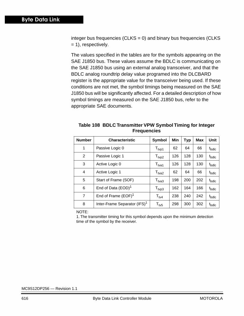
Byte Data Link
MC9S12DP256 — Revision 1.1
616 Byte Data Link Controller Module MOTOROLA
integer bus frequencies (CLKS = 0) and binary bus frequencies (CLKS = 1), respectively.
The values specified in the tables are for the symbols appearing on the SAE J1850 bus. These values assume the BDLC is communicating on the SAE J1850 bus using an external analog transceiver, and that the BDLC analog roundtrip delay value programed into the DLCBARD register is the appropriate value for the transceiver being used. If these conditions are not met, the symbol timings being measured on the SAE J1850 bus will be significantly affected. For a detailed description of how symbol timings are measured on the SAE J1850 bus, refer to the appropriate SAE documents.
Table 108 BDLC Transmitter VPW Symbol Timing for Integer Frequencies
Number Characteristic Symbol Min Typ Max Unit
1 Passive Logic 0 Ttvp1 62 64 66 tbdlc
2 Passive Logic 1 Ttvp2 126 128 130 tbdlc
3 Active Logic 0 Ttva1 126 128 130 tbdlc
4 Active Logic 1 Ttva2 62 64 66 tbdlc
5 Start of Frame (SOF) Ttva3 198 200 202 tbdlc
6 End of Data (EOD)1 Ttvp3 162 164 166 tbdlc
7 End of Frame (EOF)1 Ttv4 238 240 242 tbdlc
8 Inter-Frame Separator (IFS)1 Ttv5 298 300 302 tbdlc
NOTE:1. The transmitter timing for this symbol depends upon the minimum detection time of the symbol by the receiver.
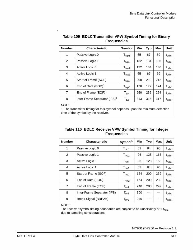
Byte Data Link Controller ModuleFunctional Description
MC9S12DP256 — Revision 1.1
MOTOROLA Byte Data Link Controller Module 617
.
Table 109 BDLC Transmitter VPW Symbol Timing for Binary Frequencies
Number Characteristic Symbol Min Typ Max Unit
1 Passive Logic 0 Ttvp1 65 67 69 tbdlc
2 Passive Logic 1 Ttvp2 132 134 136 tbdlc
3 Active Logic 0 Ttva1 132 134 136 tbdlc
4 Active Logic 1 Ttva2 65 67 69 tbdlc
5 Start of Frame (SOF) Ttva3 208 210 212 tbdlc
6 End of Data (EOD)1 Ttvp3 170 172 174 tbdlc
7 End of Frame (EOF)1 Ttv4 250 252 254 tbdlc
8 Inter-Frame Separator (IFS)1 Ttv5 313 315 317 tbdlc
NOTE:1. The transmitter timing for this symbol depends upon the minimum detection time of the symbol by the receiver.
Table 110 BDLC Receiver VPW Symbol Timing for Integer Frequencies
Number Characteristic Symbol1 Min Typ Max Unit
1 Passive Logic 0 Trvp1 32 64 95 tbdlc
2 Passive Logic 1 Trvp2 96 128 163 tbdlc
3 Active Logic 0 Trva1 96 128 163 tbdlc
4 Active Logic 1 Trva2 32 64 95 tbdlc
5 Start of Frame (SOF) Trva3 164 200 239 tbdlc
6 End of Data (EOD) Trvp3 164 200 239 tbdlc
7 End of Frame (EOF) Trv4 240 280 299 tbdlc
8 Inter-Frame Separator (IFS) Trv5 300 --- --- tbdlc
9 Break Signal (BREAK) Trv6 240 --- --- tbdlc
NOTE:The receiver symbol timing boundaries are subject to an uncertainty of 1 tbdlc due to sampling considerations.
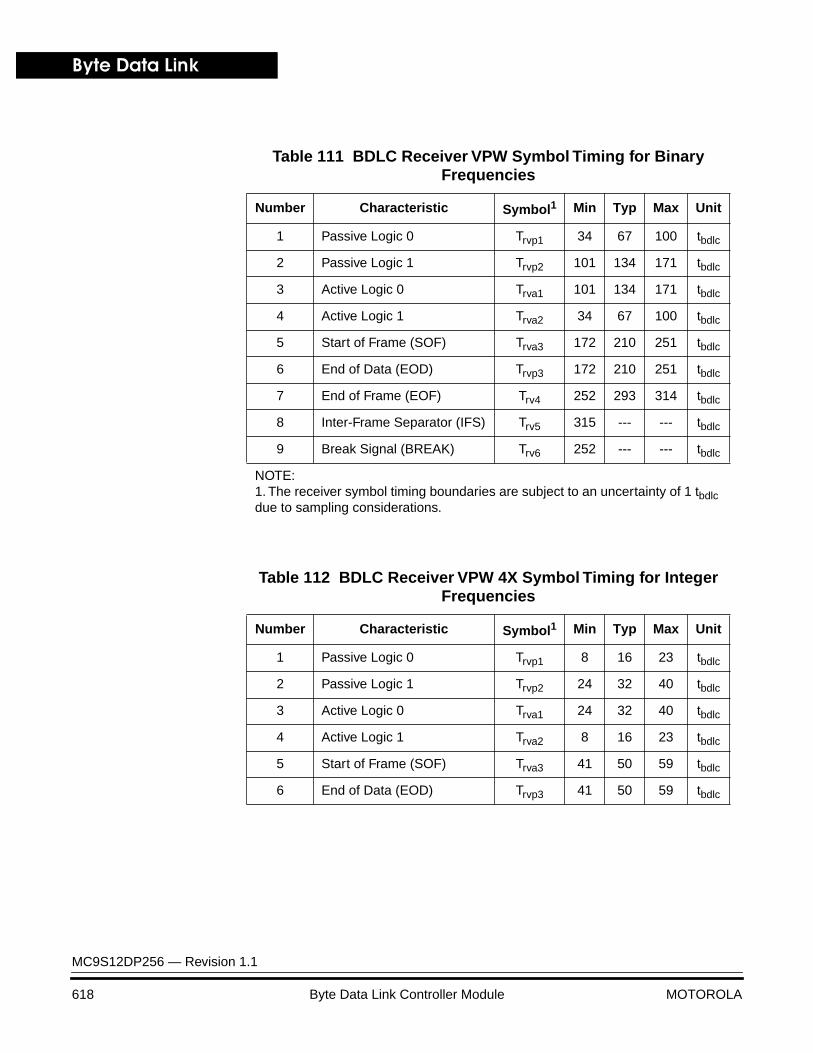
Byte Data Link
MC9S12DP256 — Revision 1.1
618 Byte Data Link Controller Module MOTOROLA
Table 111 BDLC Receiver VPW Symbol Timing for Binary Frequencies
Number Characteristic Symbol1 Min Typ Max Unit
1 Passive Logic 0 Trvp1 34 67 100 tbdlc
2 Passive Logic 1 Trvp2 101 134 171 tbdlc
3 Active Logic 0 Trva1 101 134 171 tbdlc
4 Active Logic 1 Trva2 34 67 100 tbdlc
5 Start of Frame (SOF) Trva3 172 210 251 tbdlc
6 End of Data (EOD) Trvp3 172 210 251 tbdlc
7 End of Frame (EOF) Trv4 252 293 314 tbdlc
8 Inter-Frame Separator (IFS) Trv5 315 --- --- tbdlc
9 Break Signal (BREAK) Trv6 252 --- --- tbdlc
NOTE:1. The receiver symbol timing boundaries are subject to an uncertainty of 1 tbdlc due to sampling considerations.
Table 112 BDLC Receiver VPW 4X Symbol Timing for Integer Frequencies
Number Characteristic Symbol1 Min Typ Max Unit
1 Passive Logic 0 Trvp1 8 16 23 tbdlc
2 Passive Logic 1 Trvp2 24 32 40 tbdlc
3 Active Logic 0 Trva1 24 32 40 tbdlc
4 Active Logic 1 Trva2 8 16 23 tbdlc
5 Start of Frame (SOF) Trva3 41 50 59 tbdlc
6 End of Data (EOD) Trvp3 41 50 59 tbdlc
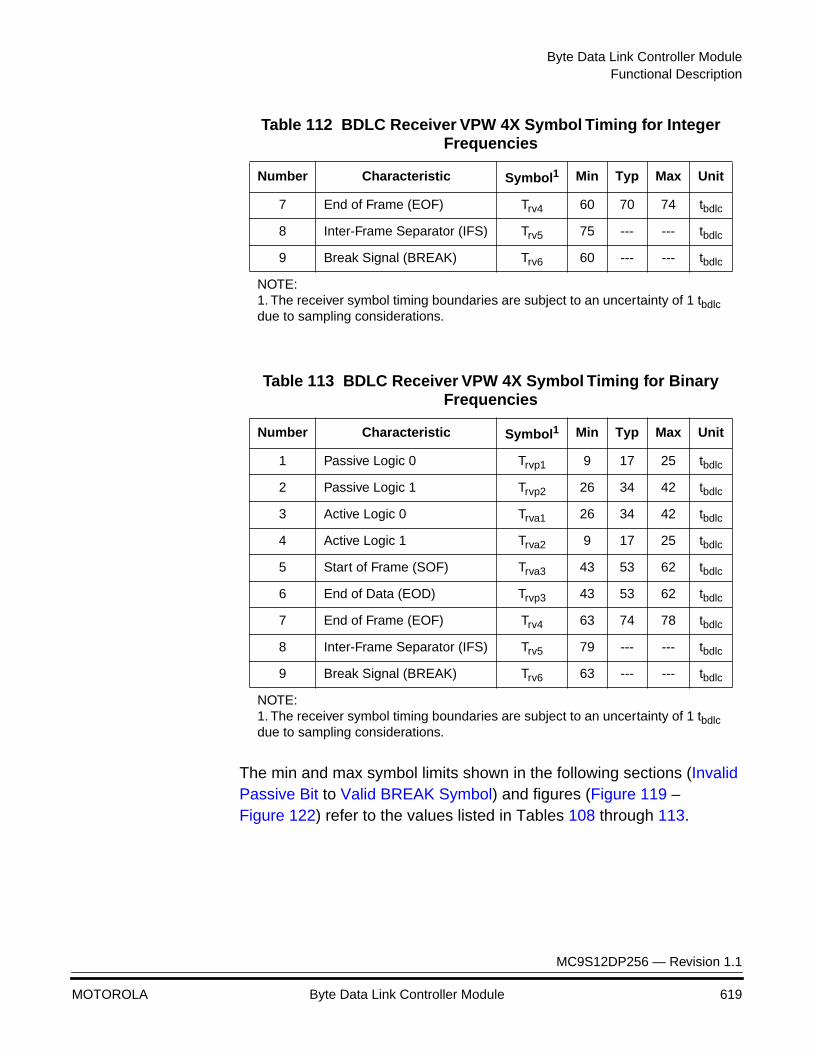
Byte Data Link Controller ModuleFunctional Description
MC9S12DP256 — Revision 1.1
MOTOROLA Byte Data Link Controller Module 619
The min and max symbol limits shown in the following sections (Invalid Passive Bit to Valid BREAK Symbol) and figures (Figure 119 – Figure 122) refer to the values listed in Tables 108 through 113.
7 End of Frame (EOF) Trv4 60 70 74 tbdlc
8 Inter-Frame Separator (IFS) Trv5 75 --- --- tbdlc
9 Break Signal (BREAK) Trv6 60 --- --- tbdlc
NOTE:1. The receiver symbol timing boundaries are subject to an uncertainty of 1 tbdlc due to sampling considerations.
Table 113 BDLC Receiver VPW 4X Symbol Timing for Binary Frequencies
Number Characteristic Symbol1 Min Typ Max Unit
1 Passive Logic 0 Trvp1 9 17 25 tbdlc
2 Passive Logic 1 Trvp2 26 34 42 tbdlc
3 Active Logic 0 Trva1 26 34 42 tbdlc
4 Active Logic 1 Trva2 9 17 25 tbdlc
5 Start of Frame (SOF) Trva3 43 53 62 tbdlc
6 End of Data (EOD) Trvp3 43 53 62 tbdlc
7 End of Frame (EOF) Trv4 63 74 78 tbdlc
8 Inter-Frame Separator (IFS) Trv5 79 --- --- tbdlc
9 Break Signal (BREAK) Trv6 63 --- --- tbdlc
NOTE:1. The receiver symbol timing boundaries are subject to an uncertainty of 1 tbdlc due to sampling considerations.
Table 112 BDLC Receiver VPW 4X Symbol Timing for Integer Frequencies
Number Characteristic Symbol1 Min Typ Max Unit
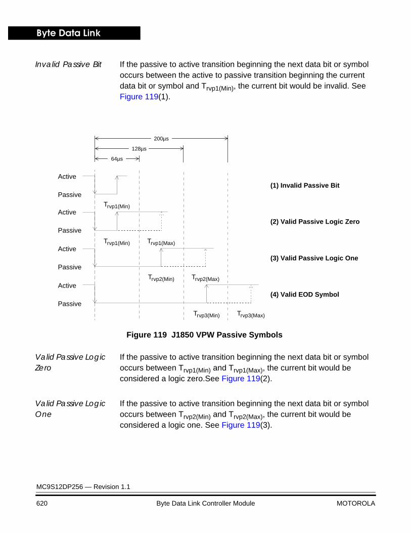
Byte Data Link
MC9S12DP256 — Revision 1.1
620 Byte Data Link Controller Module MOTOROLA
Invalid Passive Bit If the passive to active transition beginning the next data bit or symbol occurs between the active to passive transition beginning the current data bit or symbol and Trvp1(Min), the current bit would be invalid. See Figure 119(1).
Figure 119 J1850 VPW Passive Symbols
Valid Passive Logic Zero
If the passive to active transition beginning the next data bit or symbol occurs between Trvp1(Min) and Trvp1(Max), the current bit would be considered a logic zero.See Figure 119(2).
Valid Passive Logic One
If the passive to active transition beginning the next data bit or symbol occurs between Trvp2(Min) and Trvp2(Max), the current bit would be considered a logic one. See Figure 119(3).
Trvp1(Min)
Trvp2(Min) Trvp2(Max)
Trvp1(Max)Trvp1(Min)
(1) Invalid Passive Bit
(2) Valid Passive Logic Zero
(3) Valid Passive Logic One
64µs
128µs
Trvp3(Min) Trvp3(Max)
(4) Valid EOD Symbol
200µs
Active
Passive
Active
Passive
Active
Passive
Active
Passive

Byte Data Link Controller ModuleFunctional Description
MC9S12DP256 — Revision 1.1
MOTOROLA Byte Data Link Controller Module 621
Valid EOD Symbol If the passive to active transition beginning the next data bit or symbol occurs between Trvp3(Min) and Trvp3(Max), the current symbol would be considered a valid EOD symbol.See Figure 119(4).
Figure 120 J1850 VPW EOF and IFS Symbols
Valid EOF & IFS Symbol
In Figure 120(1), if the passive to active transition beginning the SOF symbol of the next message occurs between Trv4(Min) and Trv4(Max), the current symbol will be considered a valid EOF symbol.
If the passive to active transition beginning the SOF symbol of the next message occurs after Trv5(Min), the current symbol will be considered a valid EOF symbol followed by a valid IFS symbol. See Figure 120(2). All nodes must wait until a valid IFS symbol time has expired before beginning transmission. However, due to variations in clock frequencies and bus loading, some nodes may recognize a valid IFS symbol before others, and immediately begin transmitting. Therefore, anytime a node waiting to transmit detects a passive to active transition once a valid EOF has been detected, it should immediately begin transmission, initiating the arbitration process.
Idle Bus If the passive to active transition beginning the SOF symbol of the next message does not occur before Ttv5(Min), the bus is considered to be idle, and any node wishing to transmit a message may do so immediately.
(2) Valid EOF + IFS Symbol
280µs
300µs
Trv4(Min) Trv4(Max)
(1) Valid EOF Symbol Active
Passive
Active
PassiveTrv5(Min)
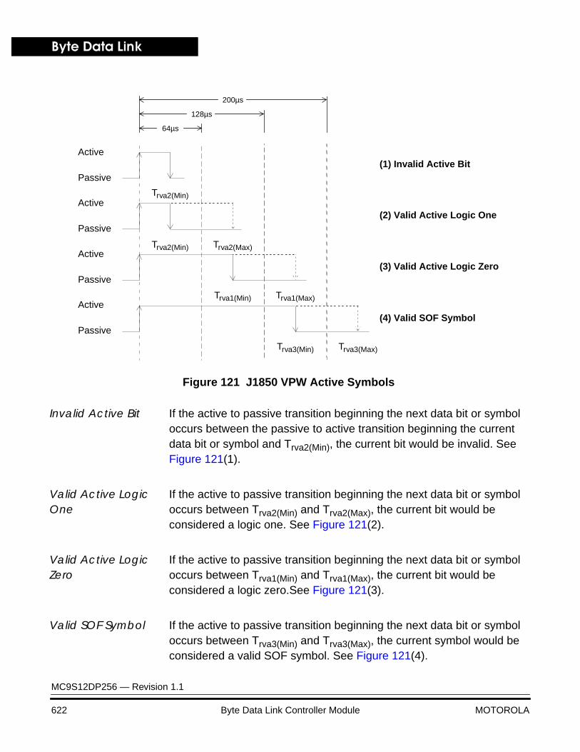
Byte Data Link
MC9S12DP256 — Revision 1.1
622 Byte Data Link Controller Module MOTOROLA
Figure 121 J1850 VPW Active Symbols
Invalid Active Bit If the active to passive transition beginning the next data bit or symbol occurs between the passive to active transition beginning the current data bit or symbol and Trva2(Min), the current bit would be invalid. See Figure 121(1).
Valid Active Logic One
If the active to passive transition beginning the next data bit or symbol occurs between Trva2(Min) and Trva2(Max), the current bit would be considered a logic one. See Figure 121(2).
Valid Active Logic Zero
If the active to passive transition beginning the next data bit or symbol occurs between Trva1(Min) and Trva1(Max), the current bit would be considered a logic zero.See Figure 121(3).
Valid SOF Symbol If the active to passive transition beginning the next data bit or symbol occurs between Trva3(Min) and Trva3(Max), the current symbol would be considered a valid SOF symbol. See Figure 121(4).
Trva2(Min)
Trva1(Min) Trva1(Max)
Trva2(Max)Trva2(Min)
(1) Invalid Active Bit
(2) Valid Active Logic One
(3) Valid Active Logic Zero
64µs
128µs
Trva3(Min) Trva3(Max)
(4) Valid SOF Symbol
200µs
Active
Passive
Active
Passive
Active
Passive
Active
Passive
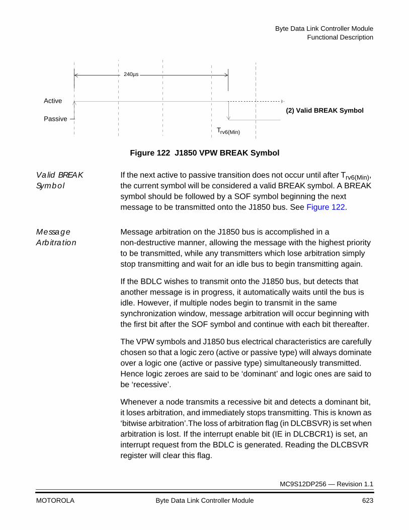
Byte Data Link Controller ModuleFunctional Description
MC9S12DP256 — Revision 1.1
MOTOROLA Byte Data Link Controller Module 623
Figure 122 J1850 VPW BREAK Symbol
Valid BREAK Symbol
If the next active to passive transition does not occur until after Trv6(Min), the current symbol will be considered a valid BREAK symbol. A BREAK symbol should be followed by a SOF symbol beginning the next message to be transmitted onto the J1850 bus. See Figure 122.
Message Arbitration
Message arbitration on the J1850 bus is accomplished in a non-destructive manner, allowing the message with the highest priority to be transmitted, while any transmitters which lose arbitration simply stop transmitting and wait for an idle bus to begin transmitting again.
If the BDLC wishes to transmit onto the J1850 bus, but detects that another message is in progress, it automatically waits until the bus is idle. However, if multiple nodes begin to transmit in the same synchronization window, message arbitration will occur beginning with the first bit after the SOF symbol and continue with each bit thereafter.
The VPW symbols and J1850 bus electrical characteristics are carefully chosen so that a logic zero (active or passive type) will always dominate over a logic one (active or passive type) simultaneously transmitted. Hence logic zeroes are said to be ‘dominant’ and logic ones are said to be ‘recessive’.
Whenever a node transmits a recessive bit and detects a dominant bit, it loses arbitration, and immediately stops transmitting. This is known as ‘bitwise arbitration’.The loss of arbitration flag (in DLCBSVR) is set when arbitration is lost. If the interrupt enable bit (IE in DLCBCR1) is set, an interrupt request from the BDLC is generated. Reading the DLCBSVR register will clear this flag.
(2) Valid BREAK Symbol
240µs
Trv6(Min)
Active
Passive
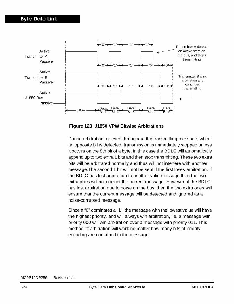
Byte Data Link
MC9S12DP256 — Revision 1.1
624 Byte Data Link Controller Module MOTOROLA
Figure 123 J1850 VPW Bitwise Arbitrations
During arbitration, or even throughout the transmitting message, when an opposite bit is detected, transmission is immediately stopped unless it occurs on the 8th bit of a byte. In this case the BDLC will automatically append up to two extra 1 bits and then stop transmitting. These two extra bits will be arbitrated normally and thus will not interfere with another message.The second 1 bit will not be sent if the first loses arbitration. If the BDLC has lost arbitration to another valid message then the two extra ones will not corrupt the current message. However, if the BDLC has lost arbitration due to noise on the bus, then the two extra ones will ensure that the current message will be detected and ignored as a noise-corrupted message.
Since a “0” dominates a “1”, the message with the lowest value will have the highest priority, and will always win arbitration, i.e. a message with priority 000 will win arbitration over a message with priority 011. This method of arbitration will work no matter how many bits of priority encoding are contained in the message.
Transmitter A
Transmitter B
J1850 Bus
SOF DataBit 1
DataBit 4
DataBit 5
“0”
Transmitter A detectsan active state onthe bus, and stops
transmitting
Transmitter B wins
Passive
Active
Passive
Active
Passive
Active
“0”
“0”
“1”
“1”
“1”
DataBit 2
“1”
“1”
“1”
DataBit 3
“0”
“0”
“0”
“0”
“1”
arbitration andcontinues
transmitting
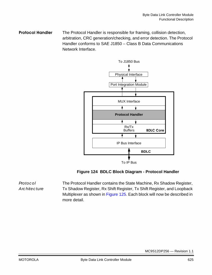
Byte Data Link Controller ModuleFunctional Description
MC9S12DP256 — Revision 1.1
MOTOROLA Byte Data Link Controller Module 625
Protocol Handler The Protocol Handler is responsible for framing, collision detection, arbitration, CRC generation/checking, and error detection. The Protocol Handler conforms to SAE J1850 – Class B Data Communications Network Interface.
Figure 124 BDLC Block Diagram - Protocol Handler
Protocol Architecture
The Protocol Handler contains the State Machine, Rx Shadow Register, Tx Shadow Register, Rx Shift Register, Tx Shift Register, and Loopback Multiplexer as shown in Figure 125. Each block will now be described in more detail.
To IP Bus
Protocol Handler
MUX Interface
IP Bus Interface
Rx/TxBuffers
Physical Interface
To J1850 Bus
BDLC
Port Integration Module
BDLC Core
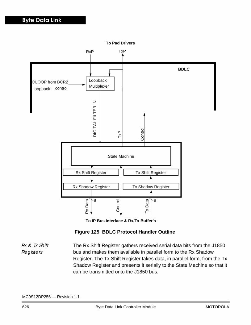
Byte Data Link
MC9S12DP256 — Revision 1.1
626 Byte Data Link Controller Module MOTOROLA
Figure 125 BDLC Protocol Handler Outline
Rx & Tx Shift Registers
The Rx Shift Register gathers received serial data bits from the J1850 bus and makes them available in parallel form to the Rx Shadow Register. The Tx Shift Register takes data, in parallel form, from the Tx Shadow Register and presents it serially to the State Machine so that it can be transmitted onto the J1850 bus.
Rx Shift Register
To IP Bus Interface & Rx/Tx Buffer’s
State Machine
To Pad Drivers
Rx
Dat
a
Tx
Dat
a
Con
trol8
Tx Shift Register
TxPDIG
ITA
L F
ILT
ER
IN
Con
trol
8
Rx Shadow Register Tx Shadow Register
Loopback
RxP
loopback control
TxP
MultiplexerDLOOP from BCR2
BDLC
Byte Data Link Controller ModuleFunctional Description
MC9S12DP256 — Revision 1.1
MOTOROLA Byte Data Link Controller Module 627
Rx & Tx Shadow Registers
Immediately after the Rx Shift Register has completed shifting in a byte of data, this data is transferred to the Rx Shadow Register and RDRF or RXIFR is set and interrupt is generated if the interrupt enable bit (IE) in BCR1 is set. After the transfer takes place, this new data byte in the Rx Shadow Register is available to the IP Bus interface, and the Rx Shift Register is ready to shift in the next byte of data. Data in Rx Shadow Register must be retrieved by the CPU before it is overwritten by new data from the Rx Shift Register.
Once the Tx Shift Register has completed its shifting operation for the current byte, the data byte in the Tx Shadow Register is loaded into the Tx Shift Register. After this transfer takes place, the Tx Shadow Register is ready to accept new data from the IP Bus.
Digital Loopback Multiplexer
The Digital Loopback Multiplexer connects the input of the receive digital filter (See Figure 125) to either the transmit signal out to the pad (TxP) or the receive signal from the pad (RxP), depending on the state of the DLOOP bit in DLCBCR2 register.
State Machine All of the functions associated with performing the protocol are executed or controlled by the State Machine. The State Machine is responsible for framing, collision detection, arbitration, CRC generation/checking, and error detection. The following sections describe the BDLC’s actions in a variety of situations.
4X Mode The BDLC can exist on the same J1850 bus as modules which use a special 4X (41.6 kbps) mode of J1850 VPW operation. The BDLC cannot transmit in 4X mode, but can receive messages in 4X mode, if the RX4X bit is set in BCR2 register. If the RX4X bit is not set in the BCR2 register, any 4X message on the J1850 bus is treated as noise by the BDLC and is ignored. Likewise, 4X messages transmitted on the SAE J1850 bus when the BDLC is in normal mode will be interpreted as noise on the network by the BDLC.
Receiving a Message in Block Mode
Although not a part of the SAE J1850 protocol, the BDLC does allow for a special “Block Mode” of operation of the receiver. As far as the BDLC is concerned, a Block Mode message is simply a long J1850 frame that

Byte Data Link
MC9S12DP256 — Revision 1.1
628 Byte Data Link Controller Module MOTOROLA
contains an indefinite number of data bytes. All of the other features of the frame remain the same, including the SOF, CRC, and EOD symbols.
Another node wishing to send a Block Mode transmission must first inform all other nodes on the network that this is about to happen. This is usually accomplished by sending a special predefined message.
Transmitting a Message in Block Mode
A Block mode message is transmitted inherently by simply loading the bytes one by one into the BDR register until the message is complete. The programmer should wait until the TDRE flag is set prior to writing a new byte of data into the BDR register. The BDLC does not contain any predefined maximum J1850 message length requirement.
J1850 Bus Errors The BDLC detects several types of transmit and receive errors which can occur during the transmission of a message onto the J1850 bus.
Transmission Error If the BDLC is transmitting a message and the message received contains a symbol error, a framing error, a bus fault, a BREAK symbol, or a logic ‘1’ symbol when a logic “0” is being transmitted, this constitutes a transmission error. Receiving a logic ‘0’ symbol when transmitting a logic ‘1’ is considered a loss of arbitration condition (See section Message Arbitration) and not a transmission error. When a transmission error is detected the BDLC will immediately cease transmitting. Further transmission or reception will be disabled until a valid EOF symbol is detected on the J1850 bus. The error condition is reflected by setting the symbol invalid or out of range flag in the DLCBSVR register. If the interrupt enable bit (IE in DLCBCR1) is set, an interrupt request from the BDLC is generated. Reading the DLCBSVR register will clear this flag.
CRC Error A cyclical redundancy check (CRC) error is detected when the data bytes and CRC byte of a received message are processed, and the CRC calculation result is not equal to $C4.The CRC code should detect any single and 2 bit errors, as well as all 8 bit burst errors, and almost all other types of errors. The CRC error flag (in DLCBSVR) is set when a CRC error is detected. If the interrupt enable bit (IE in DLCBCR1) is set, an interrupt request from the BDLC is generated. Reading the DLCBSVR register will clear this flag.
Byte Data Link Controller ModuleFunctional Description
MC9S12DP256 — Revision 1.1
MOTOROLA Byte Data Link Controller Module 629
Symbol Error A symbol error is detected when an abnormal (invalid) symbol is detected in a message being received from the J1850 bus. See sections Invalid Passive Bit and Invalid Active Bit which define invalid symbols.The symbol invalid or out of range flag (in DLCBSVR) is set when a symbol error is detected. If the interrupt enable bit (IE in DLCBCR1) is set, an interrupt request from the BDLC is generated. Reading the DLCBSVR register will clear this flag.
Framing Error A framing error is detected when a received symbol occurs in an inappropriate location in the message frame. The following situations result in framing errors:
• An active logic “0” or logic “1” received as the first symbol of the frame.
• An SOF symbol received in any location other than the first symbol of a frame. Erroneous locations include: Within the data portion of a message or IFR; Immediately following the EOD in a message or IFR.
• An EOD symbol received on a non-byte boundary in a message or IFR.
• An active logic “0” or logic “1” received immediately following the EOD at the end of an IFR.
The symbol invalid or out of range flag (in DLCBSVR) is set when a framing error is detected. If the interrupt enable bit (IE in DLCBCR1) is set, an interrupt request from the BDLC is generated. Reading the DLCBSVR register will clear this flag.
Bus Fault If a bus fault occurs, the response of the BDLC will depend upon the type of bus fault.
If the bus is shorted to VDD, the BDLC will wait for the bus to fall to a passive state before it will attempt to transmit a message. As long as the short remains, the BDLC will never attempt to transmit a message onto the J1850 bus.
If the bus is shorted to ground, the BDLC will see an idle bus, begin to transmit the message, and then detect a transmission error, since the
Byte Data Link
MC9S12DP256 — Revision 1.1
630 Byte Data Link Controller Module MOTOROLA
short to ground would not allow the bus to be driven to the active (dominant) state. The BDLC will wait for assertion of the receive pin for (64 - analog round trip delay) tbdlc cycles, after assertion of the transmit pin, before detecting the error. If the transmission is an IFR, the BDLC will wait for (280 - analog round trip delay) tbdlc cycles before detecting an error. The “analog round trip delay” is determined by the value stored in the DLCBARD register. The BDLC will set the symbol invalid or out of range flag (in DLCBSVR), abort that transmission and wait for the next IP Bus command to transmit. In this case, the transmitter does not have to wait for an EOF symbol to be received to be enabled. If the interrupt enable bit (IE in DLCBCR1) is set, an interrupt request from the BDLC is generated. Reading the DLCBSVR register will clear this flag.
In any case, if the bus fault is temporary, as soon as the fault is cleared, the BDLC will resume normal operation. If the bus fault is permanent, it may result in permanent loss of communication on the J1850 bus.
BREAK – Break Any BDLC transmitting at the time a BREAK is detected will treat the BREAK as if a transmission error had occurred, and halt transmission.
If while receiving a message the BDLC detects a BREAK symbol, it will treat the BREAK as a reception error.
If a BREAK symbol is received while the BDLC is transmitting or receiving, the symbol invalid or out of range flag (in DLCBSVR) is set. Further transmission/reception will be disabled until the J1850 bus returns to the passive state and a valid EOF symbol is detected on the J1850 bus.If the interrupt enable bit (IE in DLCBCR1) is set, an interrupt request from the BDLC is generated. Reading the DLCBSVR register will clear this flag.
The BDLC cannot transmit a BREAK symbol. It can only receive a BREAK symbol from the J1850 bus.
Bus Error Summary The possible J1850 bus errors and the actions taken by the BDLC are summarized in Table 114.
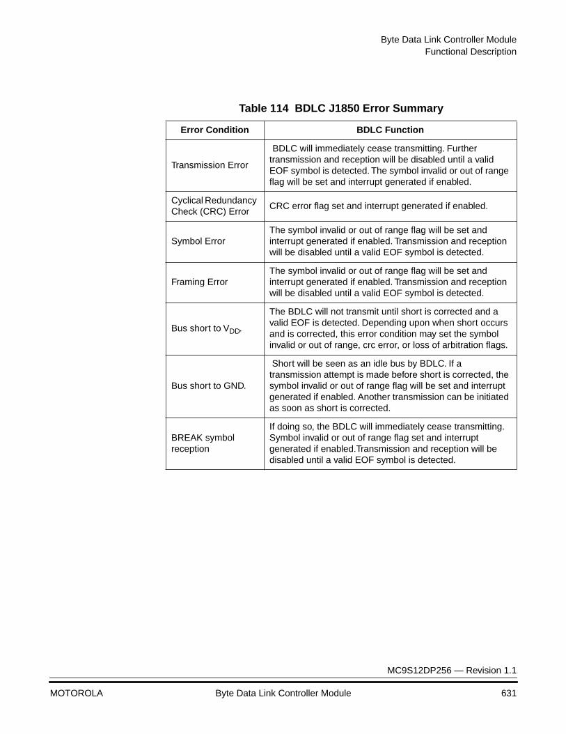
Byte Data Link Controller ModuleFunctional Description
MC9S12DP256 — Revision 1.1
MOTOROLA Byte Data Link Controller Module 631
Table 114 BDLC J1850 Error Summary
Error Condition BDLC Function
Transmission Error
BDLC will immediately cease transmitting. Further transmission and reception will be disabled until a valid EOF symbol is detected. The symbol invalid or out of range flag will be set and interrupt generated if enabled.
Cyclical Redundancy Check (CRC) Error
CRC error flag set and interrupt generated if enabled.
Symbol ErrorThe symbol invalid or out of range flag will be set and interrupt generated if enabled. Transmission and reception will be disabled until a valid EOF symbol is detected.
Framing ErrorThe symbol invalid or out of range flag will be set and interrupt generated if enabled. Transmission and reception will be disabled until a valid EOF symbol is detected.
Bus short to VDD.
The BDLC will not transmit until short is corrected and a valid EOF is detected. Depending upon when short occurs and is corrected, this error condition may set the symbol invalid or out of range, crc error, or loss of arbitration flags.
Bus short to GND.
Short will be seen as an idle bus by BDLC. If a transmission attempt is made before short is corrected, the symbol invalid or out of range flag will be set and interrupt generated if enabled. Another transmission can be initiated as soon as short is corrected.
BREAK symbol reception
If doing so, the BDLC will immediately cease transmitting. Symbol invalid or out of range flag set and interrupt generated if enabled.Transmission and reception will be disabled until a valid EOF symbol is detected.

Byte Data Link
MC9S12DP256 — Revision 1.1
632 Byte Data Link Controller Module MOTOROLA
IP Bus Interface
Figure 126 BDLC Block Diagram - IP Bus Interface
The IP Bus Interface provides the interface between the IP Bus and the rest of the BDLC. The address space of the BDLC is continuous, consisting of 8 bytes starting at the base address. The base address of the module is hardware programmable as defined by the IP Bus Specification.
The register decode map is fixed and begins at the first address of the Module Base Address. Table 107 in Register Map shows the registers associated with the BDLC module and their relative offset from the base address.
To IP Bus
Protocol Handler
MUX Interface
IP Bus Interface
Rx/TxBuffers
Physical Interface
To J1850 Bus
BDLC
Port Integration Module
BDLC Core

Byte Data Link Controller ModuleRegister Descriptions
MC9S12DP256 — Revision 1.1
MOTOROLA Byte Data Link Controller Module 633
Register Descriptions
NOTE: All bits of all registers in this module are completely synchronous to internal clocks during a register read.
BDLC Control Register 1 (DLCBCR1)
This register is used to configure and control the BDLC.
READ: any time
WRITE: IMSG, IE, and WCM any time.
CLKS write once in normal and emulation modes.
CLKS bit has modified functionality in special test mode.
Writes to unimplemented bits 5-2 are ignored.
IMSG — Ignore Message (Bit 7)
This bit allows the CPU to ignore messages by disabling updates of the DLCBSVR register until a new Start of Frame (SOF) or a BREAK symbol is detected. BDLC transmitter and receiver operation are unaffected by the state of the IMSG bit.
1 = Disable DLCBSVR Updates. When set, all BDLC interrupt sources (exceptions are described below) will be prevented from updating DLCBSVR status bits. Setting IMSG does not clear pending interrupt flags, the behavior of which will still be as described in BDLC State Vector Register (DLCBSVR). If this bit is set while the BDLC is receiving or transmitting a message, state vector register updates will be inhibited for the rest of the message.
Address Offset: $0000
Bit 7 6 5 4 3 2 1 Bit 0
Read:IMSG CLKS
0 0 0 0IE WCM
Write:
Reset: 1 1 0 0 0 0 0 0
= Unimplemented
Byte Data Link
MC9S12DP256 — Revision 1.1
634 Byte Data Link Controller Module MOTOROLA
0 = Enable DLCBSVR Updates. This bit is automatically cleared by the reception of a SOF symbol or a BREAK symbol. It will then allow updates of the state vector register to occur.
There are two situations in which interrupts will not be masked by the IMSG bit: when a wakeup interrupt occurs; and when a receiver error occurs which causes a byte pending transmission to be flushed from the transmit shadow register. See BDLC Data Register (DLCBDR) for a description of the conditions which cause a pending transmission to be flushed.
CLKS — Clock Select (Bit 6)
The nominal BDLC operating frequency (mux interface clock frequency - fbdlc) must always be 1.048576 MHz or 1 MHz in order for
J1850 bus communications to take place properly. The CLKS register bit is provided to allow the user to indicate to the BDLC which frequency (1.048576 MHz or 1 MHz) is used so that each symbol time can be automatically adjusted.
The CLKS bit is a write once bit. All writes to this bit will be ignored after the first one.
1 = Binary frequency (1.048576 MHz) is used for fbdlc.
0 = Integer frequency (1 MHz) is used. for fbdlc
J1850 VPW Valid/Invalid Bits & Symbols describes the transmitter and receiver VPW symbol timing for integer and binary frequencies.
IE — Interrupt Enable (Bit 1)
This bit determines whether the BDLC will generate CPU interrupt requests. It does not affect CPU interrupt requests when exiting the BDLC Stop or Wait modes. Interrupt requests will be maintained until all of the interrupt request sources are cleared, by performing the specified actions upon the BDLC’s registers. Interrupts that were pending at the time that this bit is cleared may be lost.
1 = Enable interrupt requests from BDLC0 = Disable interrupt requests from BDLC
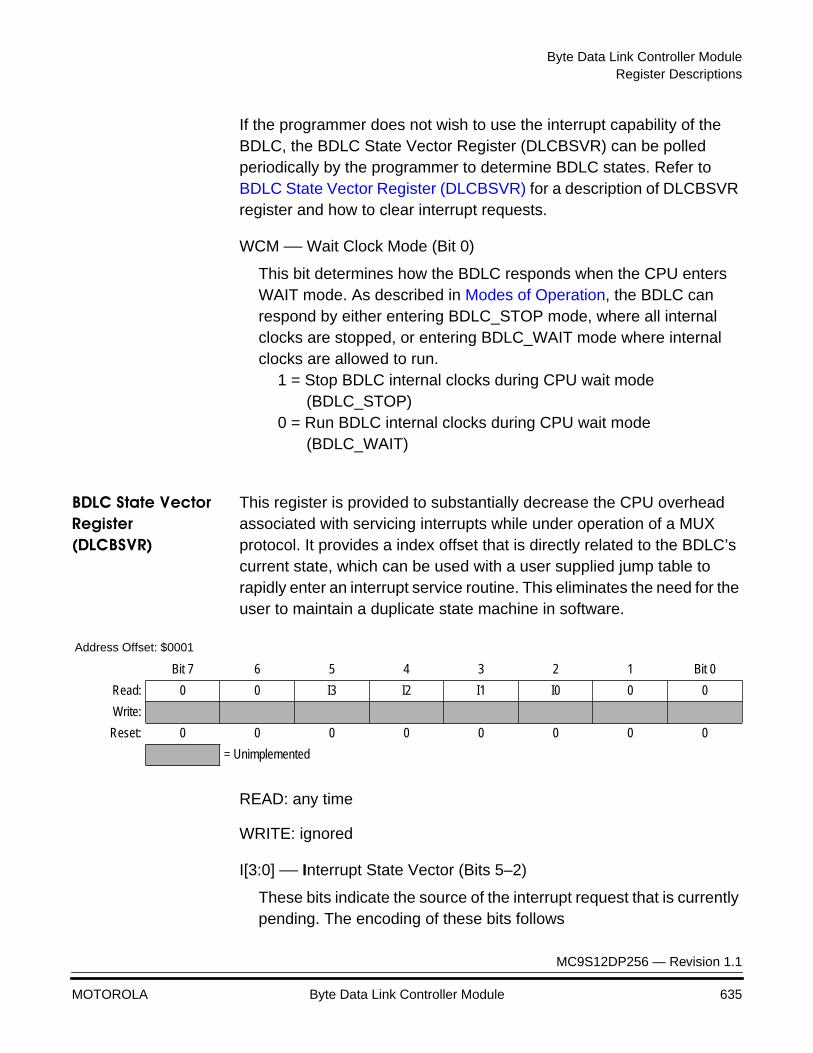
Byte Data Link Controller ModuleRegister Descriptions
MC9S12DP256 — Revision 1.1
MOTOROLA Byte Data Link Controller Module 635
If the programmer does not wish to use the interrupt capability of the BDLC, the BDLC State Vector Register (DLCBSVR) can be polled periodically by the programmer to determine BDLC states. Refer to BDLC State Vector Register (DLCBSVR) for a description of DLCBSVR register and how to clear interrupt requests.
WCM — Wait Clock Mode (Bit 0)
This bit determines how the BDLC responds when the CPU enters WAIT mode. As described in Modes of Operation, the BDLC can respond by either entering BDLC_STOP mode, where all internal clocks are stopped, or entering BDLC_WAIT mode where internal clocks are allowed to run.
1 = Stop BDLC internal clocks during CPU wait mode (BDLC_STOP)
0 = Run BDLC internal clocks during CPU wait mode (BDLC_WAIT)
BDLC State Vector Register (DLCBSVR)
This register is provided to substantially decrease the CPU overhead associated with servicing interrupts while under operation of a MUX protocol. It provides a index offset that is directly related to the BDLC’s current state, which can be used with a user supplied jump table to rapidly enter an interrupt service routine. This eliminates the need for the user to maintain a duplicate state machine in software.
READ: any time
WRITE: ignored
I[3:0] — Interrupt State Vector (Bits 5–2)
These bits indicate the source of the interrupt request that is currently pending. The encoding of these bits follows
Address Offset: $0001
Bit 7 6 5 4 3 2 1 Bit 0
Read: 0 0 I3 I2 I1 I0 0 0
Write:
Reset: 0 0 0 0 0 0 0 0
= Unimplemented
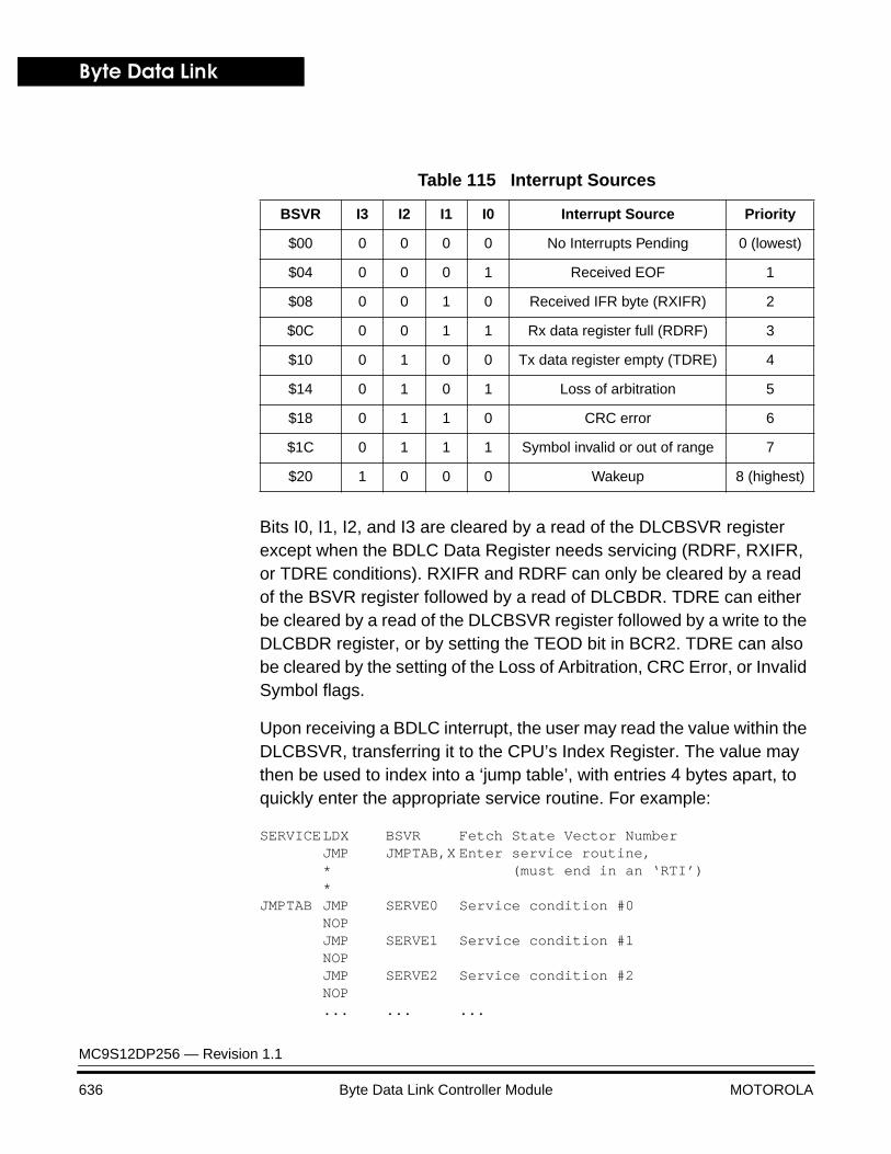
Byte Data Link
MC9S12DP256 — Revision 1.1
636 Byte Data Link Controller Module MOTOROLA
Bits I0, I1, I2, and I3 are cleared by a read of the DLCBSVR register except when the BDLC Data Register needs servicing (RDRF, RXIFR, or TDRE conditions). RXIFR and RDRF can only be cleared by a read of the BSVR register followed by a read of DLCBDR. TDRE can either be cleared by a read of the DLCBSVR register followed by a write to the DLCBDR register, or by setting the TEOD bit in BCR2. TDRE can also be cleared by the setting of the Loss of Arbitration, CRC Error, or Invalid Symbol flags.
Upon receiving a BDLC interrupt, the user may read the value within the DLCBSVR, transferring it to the CPU’s Index Register. The value may then be used to index into a ‘jump table’, with entries 4 bytes apart, to quickly enter the appropriate service routine. For example:
SERVICELDX BSVR Fetch State Vector NumberJMP JMPTAB,X Enter service routine,* (must end in an ‘RTI’)*
JMPTAB JMP SERVE0 Service condition #0NOPJMP SERVE1 Service condition #1NOPJMP SERVE2 Service condition #2NOP... ... ...
Table 115 Interrupt Sources
BSVR I3 I2 I1 I0 Interrupt Source Priority
$00 0 0 0 0 No Interrupts Pending 0 (lowest)
$04 0 0 0 1 Received EOF 1
$08 0 0 1 0 Received IFR byte (RXIFR) 2
$0C 0 0 1 1 Rx data register full (RDRF) 3
$10 0 1 0 0 Tx data register empty (TDRE) 4
$14 0 1 0 1 Loss of arbitration 5
$18 0 1 1 0 CRC error 6
$1C 0 1 1 1 Symbol invalid or out of range 7
$20 1 0 0 0 Wakeup 8 (highest)
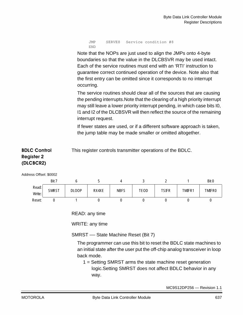
Byte Data Link Controller ModuleRegister Descriptions
MC9S12DP256 — Revision 1.1
MOTOROLA Byte Data Link Controller Module 637
JMP SERVE8 Service condition #8END
Note that the NOPs are just used to align the JMPs onto 4-byte boundaries so that the value in the DLCBSVR may be used intact. Each of the service routines must end with an ‘RTI’ instruction to guarantee correct continued operation of the device. Note also that the first entry can be omitted since it corresponds to no interrupt occurring.
The service routines should clear all of the sources that are causing the pending interrupts.Note that the clearing of a high priority interrupt may still leave a lower priority interrupt pending, in which case bits I0, I1 and I2 of the DLCBSVR will then reflect the source of the remaining interrupt request.
If fewer states are used, or if a different software approach is taken, the jump table may be made smaller or omitted altogether.
BDLC Control Register 2 (DLCBCR2)
This register controls transmitter operations of the BDLC.
READ: any time
WRITE: any time
SMRST — State Machine Reset (Bit 7)
The programmer can use this bit to reset the BDLC state machines to an initial state after the user put the off-chip analog transceiver in loop back mode.
1 = Setting SMRST arms the state machine reset generation logic.Setting SMRST does not affect BDLC behavior in any way.
Address Offset: $0002
Bit 7 6 5 4 3 2 1 Bit 0
Read:SMRST DLOOP RX4XE NBFS TEOD TSIFR TMIFR1 TMIFR0
Write:
Reset: 0 1 0 0 0 0 0 0
Byte Data Link
MC9S12DP256 — Revision 1.1
638 Byte Data Link Controller Module MOTOROLA
0 = Clearing SMRST after it has been set will cause the generation of a state machine reset.After SMRST is cleared, the BDLC requires the bus to be idle for a minimum of an End of Frame symbol (EOF) time before allowing the reception of a message. The BDLC requires the bus to be idle for a minimum of an Inter-Frame Separator symbol (IFS) time before allowing any message to be transmitted.
DLOOP — Digital Loopback Mode (Bit 6)
This bit determines the source to which the input of the digital filter is connected and can be used to isolate bus fault conditions. If a fault condition has been detected on the bus, this control bit allows the programmer to disconnect the digital filter from input from the receive pin (RxP) and connect it to the transmit output to the pin (TxP). In this configuration, data sent from the transmit buffer should be reflected back into the receive buffer. If no faults exist in the digital block, the fault is in the physical interface block or elsewhere on the J1850 bus.
1 = When set, digital filter input is connected to the transmitter output. The BDLC is now in Digital Loopback Mode of operation. The transmit pin (TxP) is driven low and not driven by the transmitter output.
0 = When cleared, digital filter input is connected to receive pin (RxP) and the transmitter output is connected to the transmit pin (TxP). The BDLC is taken out of Digital Loopback Mode and can now drive and receive from the J1850 bus normally. After writing DLOOP to zero, the BDLC requires the bus to be idle for a minimum of and End of Frame symbol time before allowing a reception of a message. The BDLC requires the bus to be idle for a minimum of an Inter-Frame Separator symbol time before allowing any message to be transmitted.
NOTE: The DLOOP bit is a fault condition aid and should never be altered after the DLCBDR is loaded for transmission. Changing DLOOP during a transmission may cause corrupted data to be transmitted onto the J1850 network.

Byte Data Link Controller ModuleRegister Descriptions
MC9S12DP256 — Revision 1.1
MOTOROLA Byte Data Link Controller Module 639
RX4XE — Receive 4X Enable (Bit 5)
This bit determines if the BDLC operates at normal transmit and receive speed (10.4 kbps) or receive only at 41.6 kbps. This feature is useful for fast download of data into a J1850 node for diagnostic or factory programming of the node.
1 = When set, the BDLC is put in 4X (41.6 kbps) receive only operation.
0 = When cleared, the BDLC transmits and receives at 10.4 kbps. Reception of a BREAK symbol automatically clears this bit and sets the symbol invalid or out of range flag (DLCBSVR = $1C).
The effect of 4X receive operation on receive symbol timing boundaries is described in section Transmit and Receive Symbol Timing Specifications.The RX4XE bit is not affected by entry or exit from BDLC stop or wait modes.
NBFS — Normalization Bit Format Select (Bit 4)
This bit controls the format of the Normalization Bit (NB). SAE J1850 strongly encourages the use of an active long, ‘0’, for In-Frame Responses containing CRC and active short, ‘1’, for In-Frame Responses without CRC.
1 = NB that is received or transmitted is a ‘0’ when the response part of an In-Frame Response (IFR) ends with a CRC byte. NB that is received or transmitted is a ‘1’ when the response part of an In-Frame Response (IFR) does not end with a CRC byte.
0 = NB that is received or transmitted is a ‘1’ when the response part of an In-Frame Response (IFR) ends with a CRC byte. NB that is received or transmitted is a ‘0’ when the response part of an In-Frame Response (IFR) does not end with a CRC byte.
TEOD — Transmit End of Data (Bit 3)
This bit is set by the programmer to indicate the end of a message being sent by the BDLC. It will append an 8-bit CRC after completing transmission of the current byte in the Tx Shift Register followed by the EOD symbol. If the transmit shadow register (refer to Rx & Tx Shadow Registers for a description of the transmit shadow register) is full when TEOD is set, the CRC byte and EOD will be transmitted after the current byte in the Tx Shift Register and the byte in the Tx

Byte Data Link
MC9S12DP256 — Revision 1.1
640 Byte Data Link Controller Module MOTOROLA
Shadow Register have been transmitted. Once TEOD is set, the transmit data register empty flag (TDRE) in the BDLC State Vector Register (DLCBSVR) is cleared to allow lower priority interrupts to occur. This bit is also used to end an IFR. Bits TSIFR, TMIFR1, and TMIFR0 determine whether a CRC byte is appended before EOD transmission for IFRs.
1 = Transmit EOD symbol. 0 = The TEOD bit will be automatically cleared after the first CRC
bit is sent, or if an error or loss of arbitration is detected on the bus. When TEOD is used to end an IFR transmission, TEOD is cleared when the BDLC receives back a valid EOD symbol, or an error condition or loss of arbitration occurs.
TSIFR, TMIFR1, TMIFR0 — Transmit In-Frame Response Control (Bits 2-0)
These three bits control the type of In-Frame Response being sent. The programmer should not set more than one of these control bits to a one at any given time. However, if more than one of these three control bits are set to one, the priority encoding logic will force the internal register bits to a known value as shown in the following table. But, when these bits are read, they will be the same as written earlier. For instance, if “011” is written to TSIFR, TMIFR1, TMIFR0, then internally, they’ll be encoded as “010”. However, when these bits are later read back, it’ll still be “011”.
Table 116 Transmit In-Frame Response Control Bit Priority Encoding
Write Read Actual (internal register)
TSIFR TMIFR1 TMIFR0 TSIFR TMIFR1 TMIFR0 TSIFR TMIFR1 TMIFR0
0 0 0 0 0 0 0 0 0
1 X X 1 X X 1 0 0
0 1 X 0 1 X 0 1 0
0 0 1 0 0 1 0 0 1
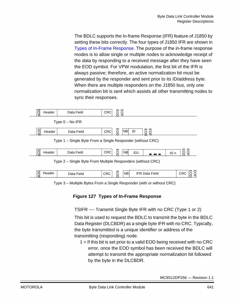
Byte Data Link Controller ModuleRegister Descriptions
MC9S12DP256 — Revision 1.1
MOTOROLA Byte Data Link Controller Module 641
The BDLC supports the In-frame Response (IFR) feature of J1850 by setting these bits correctly. The four types of J1850 IFR are shown in Types of In-Frame Response. The purpose of the in-frame response modes is to allow single or multiple nodes to acknowledge receipt of the data by responding to a received message after they have seen the EOD symbol. For VPW modulation, the first bit of the IFR is always passive; therefore, an active normalization bit must be generated by the responder and sent prior to its ID/address byte. When there are multiple responders on the J1850 bus, only one normalization bit is sent which assists all other transmitting nodes to sync their responses.
Figure 127 Types of In-Frame Response
TSIFR — Transmit Single Byte IFR with no CRC (Type 1 or 2)
This bit is used to request the BDLC to transmit the byte in the BDLC Data Register (DLCBDR) as a single byte IFR with no CRC. Typically, the byte transmitted is a unique identifier or address of the transmitting (responding) node.
1 = If this bit is set prior to a valid EOD being received with no CRC error, once the EOD symbol has been received the BDLC will attempt to transmit the appropriate normalization bit followed by the byte in the DLCBDR.
SO
F Header Data Field CRCE
OD
Type 0 – No IFR
Header Data Field CRC
EO
D
Type 3 – Multiple Bytes From a Single Responder (with or without CRC)
Header Data Field CRC
EO
D
Type 1 – Single Byte From a Single Responder (without CRC)
Header Data Field CRC
EO
D
Type 2 – Single Byte From Multiple Responders (without CRC)
ID1 ID n
IFR Data Field CRC
NB
NB
NB
ID
SO
FS
OF
SO
F
EO
F
EO
DE
OF
EO
DE
OF
EO
DE
OF
Byte Data Link
MC9S12DP256 — Revision 1.1
642 Byte Data Link Controller Module MOTOROLA
0 = The TSIFR bit will be automatically cleared once the EOD following one or more IFR bytes has been received or an error is detected on the bus.
The user must set the TSIFR bit before the EOF following the main part of the message frame is received, or no IFR transmit attempts will be made for the current message. If another node transmits an IFR to this message, the user must set the TSIFR bit before the normalization bit is received or no IFR transmit attempts will be made for the message. If another node does transmit a successful IFR or a reception error occurs, the TSIFR bit will be cleared. If not, the IFR will be transmitted after the EOD of the next received message.
If a loss of arbitration occurs when the BDLC attempts transmission, after the IFR byte winning arbitration completes transmission, the BDLC will again attempt to transmit the byte in the DLCBDR (with no normalization bit). The BDLC will continue transmission attempts until an error is detected on the bus, or TEOD is set by the CPU, or the BDLC transmission is successful.
NOTE: Setting the TEOD bit before transmission of the IFR byte will direct the BDLC to make only one attempt at transmitting the byte.
If loss of arbitration occurs in the last bit of the IFR byte, two additional ‘1’ bits will not be sent out because the BDLC will attempt to retransmit the byte in the transmit shift register after the IFR byte winning arbitration completes transmission.
TMIFR1 — Transmit Multiple Byte IFR with CRC (Type 3)
This bit requests the BDLC to transmit the byte in the BDLC Data Register (DLCBDR) as the first byte of a multiple byte IFR with CRC or as a single byte IFR with CRC.Response IFR bytes are still subject to J1850 message length maximums.
1 = If this bit is set prior to a valid EOD being received with no CRC error, once the EOD symbol has been received the BDLC will attempt to transmit the appropriate normalization bit followed by IFR bytes.The programmer should set TEOD after the last IFR byte has been written into DLCBDR register. After TEOD has been set and the last IFR byte has been transmitted, the CRC byte is transmitted.
Byte Data Link Controller ModuleRegister Descriptions
MC9S12DP256 — Revision 1.1
MOTOROLA Byte Data Link Controller Module 643
0 = The TMIFR1 bit will be automatically cleared once the BDLC has successfully transmitted the CRC byte and EOD symbol, by the detection of an error on the multiplex bus, a transmitter underrun, or loss of arbitration.
After the byte in the DLCBDR has been loaded into the transmit shift register, the TDRE flag will be set in the DLCBSVR register, similar to the main message transmit sequence. If the interrupt enable bit (IE in DLCBCR1) is set, an interrupt request from the BDLC is generated.The programmer should then load the next byte of the IFR into the DLCBDR for transmission. When the last byte of the IFR has been loaded into the DLCBDR, the programmer should set the TEOD bit in the BDLC control register 2 (DLCBCR2). This will instruct the BDLC to transmit a CRC byte once the byte in the DLCBDR is transmitted, and then transmit an EOD symbol, indicating the end of the IFR portion of the message frame.
However, if the programmer wishes to transmit a single byte followed by a CRC byte, the programmer should load the byte into the DLCBDR and then set the TMIFR1 bit before the EOD symbol has been received. Once the TDRE flag is set and interrupt occurs (if enabled), the programmer should then set the TEOD bit in DLCBCR2. This will result in the byte in the DLCBDR being the only byte transmitted before the IFR CRC byte.
The user must set the TMIFR1 bit before the EOF following the main part of the message frame is received, or no IFR transmit attempts will be made for the current message. If another node transmits an IFR to this message, the user must set the TMIFR1 bit before the normalization bit is received or no IFR transmit attempts will be made for the message. If another node does transmit a successful IFR or a reception error occurs, the TMIFR1 bit will be cleared. If not, the IFR will be transmitted after the EOD of the next received message.
If a transmitter underrun error occurs during transmission (caused by the programmer not writing another byte to the DLCBDR following the TDRE flag being set) the BDLC will automatically disable the transmitter after the byte currently in the shifter plus two extra 1-bits have been transmitted. The receiver will pick this up as an framing error and relay it in the State Vector Register as an invalid symbol error. The TMIFR1 bit will also be cleared.
Byte Data Link
MC9S12DP256 — Revision 1.1
644 Byte Data Link Controller Module MOTOROLA
If a loss of arbitration occurs when the BDLC is transmitting a multiple byte IFR with CRC, the BDLC will go to the loss of arbitration state, set the appropriate flag and cease transmission. The TMIFR1 bit will be cleared and no attempt will be made to retransmit the byte in the DLCBDR. If loss of arbitration occurs in the last bit of the IFR byte, two additional one bits (a passive long followed by an active short) will be sent out.
NOTE: The extra logic 1s are an enhancement to the J1850 protocol which forces a byte boundary condition fault. This is helpful in preventing noise on the J1850 bus from corrupting a message.
TMIFR0 — Transmit Multiple Byte IFR with no CRC (Type 3)
This bit is used to request the BDLC to transmit the byte in the BDLC Data Register (DLCBDR) as the first byte of a multiple byte IFR without CRC. Response IFR bytes are still subject to J1850 message length maximums.
1 = If this bit is set prior to a valid EOD being received with no CRC error, once the EOD symbol has been received the BDLC will attempt to transmit the appropriate normalization bit followed by IFR bytes. The programmer should set TEOD after the last IFR byte has been written into DLCBDR register. After TEOD has been set, the last IFR byte to be transmitted will be the last byte which was written into the DLCBDR register.
0 = The TMIFR0 bit will be automatically cleared once the BDLC has successfully transmitted the EOD symbol, by the detection of an error on the multiplex bus, a transmitter underrun, or loss of arbitration.
After the byte in the DLCBDR has been loaded into the transmit shift register, the TDRE flag will be set in the DLCBSVR register, similar to the main message transmit sequence. If the interrupt enable bit (IE in DLCBCR1) is set, an interrupt request from the BDLC is generated. The programmer should then load the next byte of the IFR into the DLCBDR for transmission. When the last byte of the IFR has been loaded into the DLCBDR, the programmer should set the TEOD bit in the DLCBCR2 register. This will instruct the BDLC to transmit an EOD symbol, indicating the end of the IFR portion of the message frame. The BDLC will not append a CRC.
Byte Data Link Controller ModuleRegister Descriptions
MC9S12DP256 — Revision 1.1
MOTOROLA Byte Data Link Controller Module 645
However, if the programmer wishes to transmit a single byte, the programmer should load the byte into the DLCBDR and then set the TMIFR0 bit before the EOD symbol has been received. Once the TDRE flag is set and interrupt occurs (if enabled), the programmer should then set the TEOD bit in DLCBCR2. This will result in the byte in the DLCBDR being the only byte transmitted.
The user must set the TMIFR0 bit before the EOF following the main part of the message frame is received, or no IFR transmit attempts will be made for the current message. If another node transmits an IFR to this message, the user must set the TMIFR0 bit before the normalization bit is received or no IFR transmit attempts will be made for the message. If another node does transmit a successful IFR or a reception error occurs, the TMIFR0 bit will be cleared. If not, the IFR will be transmitted after the EOD of the next received message.
If a transmitter underrun error occurs during transmission (caused by the programmer not writing another byte to the DLCBDR following the TDRE flag being set) the BDLC will automatically disable the transmitter after the byte currently in the shifter plus two extra 1-bits have been transmitted. The receiver will pick this up as an framing error and relay it in the State Vector Register as an invalid symbol error. The TMIFR0 bit will also be cleared.
If a loss of arbitration occurs when the BDLC is transmitting a multiple byte IFR without CRC, the BDLC will go to the loss of arbitration state, set the appropriate flag and cease transmission. The TMIFR0 bit will be cleared and no attempt will be made to retransmit the byte in the DLCBDR. If loss of arbitration occurs in the last bit of the IFR byte, two additional one bits (a passive long followed by an active short) will be sent out.
NOTE: The extra logic 1s are an enhancement to the J1850 protocol which forces a byte boundary condition fault. This is helpful in preventing noise on the J1850 bus from corrupting a message.

Byte Data Link
MC9S12DP256 — Revision 1.1
646 Byte Data Link Controller Module MOTOROLA
BDLC Data Register (DLCBDR)
This register is used to pass the data to be transmitted to the J1850 bus from the CPU to the BDLC. It is also used to pass data received from the J1850 bus to the CPU.
READ: any time
WRITE: any time
D7:D0 — Receive/Transmit Data (Bits 7 - 0)
Each data byte (after the first one) should be written only after a “Tx Data Register Empty” (TDRE) interrupt has occurred, or the DLCBSVR register has been polled indicating this condition.
Data read from this register will be the last data byte received from the J1850 bus. This received data should only be read after a “Rx Data Register Full” (RDRF) or “Received IFR byte” (RXIFR) interrupt has occurred or the DLCBSVR register has been polled indicating either of these two conditions.
The DLCBDR register is double buffered via a transmit shadow register and a receive shadow register. After the byte in the transmit shift register has been transmitted, the byte currently stored in the transmit shadow register is loaded into the transmit shift register. Once the transmit shift register has shifted the first bit out, the TDRE flag is set, and the shadow register is ready to accept the next byte of data.
The receive shadow register works similarly. Once a complete byte has been received, the receive shift register stores the newly received byte into the receive shadow register. The RDRF flag (or RXIFR flag if the received byte is part of an IFR) is set to indicate that a new byte of data has been received. The programmer has one BDLC byte reception time to read the shadow register and clear the RDRF or RXIFR flag before the shadow register is overwritten by the newly received byte.
Address Offset: $0003
Bit 7 6 5 4 3 2 1 Bit 0
Read:D7 D6 D5 D4 D3 D2 D1 D0
Write:
Reset: 0 0 0 0 0 0 0 0
Byte Data Link Controller ModuleRegister Descriptions
MC9S12DP256 — Revision 1.1
MOTOROLA Byte Data Link Controller Module 647
If the user writes the first byte of a message to be transmitted to the DLCBDR and then determines that a different message should be transmitted, the user can write a new byte to the DLCBDR up until the transmission begins.This new byte will replace the original byte in the DLCBDR.
From the time a byte is written to the DLCBDR until it is transferred to the transmit shift register, the transmit shadow register is considered full and the byte pending transmission. If one of the IFR transmission control bits (TSIFR, TMIFR1, or TMIFR0 in DLCBCR2) is also set, the byte is pending transmission as an IFR. A byte pending transmission will be flushed from the transmit shadow register and the transmission canceled if one of the following occurs: a loss of arbitration or transmitter error on the byte currently being transmitted; a symbol error, framing error, bus fault, or BREAK symbol is received. If the byte pending transmission is an IFR byte, the reception of a message with a CRC error will also cause the byte in the transmit shadow register to be flushed.
To abort an in-progress transmission, the programmer should simply stop loading more data into the BDR. This will cause a transmitter underrun error and the BDLC will automatically disable the transmitter on the next non-byte boundary. This means that the earliest a transmission can be halted is after at least one byte (plus two extra 1-bits) has been transmitted. The receiver will pick this up as an error and relay it in the State Vector Register as an invalid symbol error.
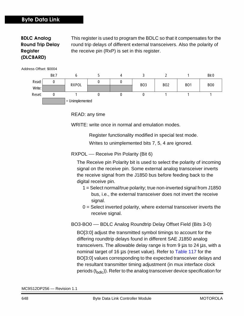
Byte Data Link
MC9S12DP256 — Revision 1.1
648 Byte Data Link Controller Module MOTOROLA
BDLC Analog Round Trip Delay Register (DLCBARD)
This register is used to program the BDLC so that it compensates for the round trip delays of different external transceivers. Also the polarity of the receive pin (RxP) is set in this register.
READ: any time
WRITE: write once in normal and emulation modes.
Register functionality modified in special test mode.
Writes to unimplemented bits 7, 5, 4 are ignored.
RXPOL — Receive Pin Polarity (Bit 6)
The Receive pin Polarity bit is used to select the polarity of incoming signal on the receive pin. Some external analog transceiver inverts the receive signal from the J1850 bus before feeding back to the digital receive pin.
1 = Select normal/true polarity; true non-inverted signal from J1850 bus, i.e., the external transceiver does not invert the receive signal.
0 = Select inverted polarity, where external transceiver inverts the receive signal.
BO3-BO0 — BDLC Analog Roundtrip Delay Offset Field (Bits 3-0)
BO[3:0] adjust the transmitted symbol timings to account for the differing roundtrip delays found in different SAE J1850 analog transceivers. The allowable delay range is from 9 µs to 24 µs, with a nominal target of 16 µs (reset value). Refer to Table 117 for the BO[3:0] values corresponding to the expected transceiver delays and the resultant transmitter timing adjustment (in mux interface clock periods (tbdlc)). Refer to the analog transceiver device specification for
Address Offset: $0004
Bit 7 6 5 4 3 2 1 Bit 0
Read: 0RXPOL
0 0BO3 BO2 BO1 BO0
Write:
Reset: 0 1 0 0 0 1 1 1
= Unimplemented
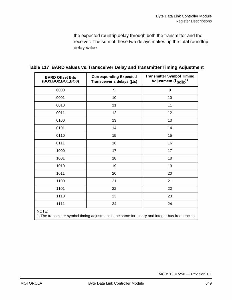
Byte Data Link Controller ModuleRegister Descriptions
MC9S12DP256 — Revision 1.1
MOTOROLA Byte Data Link Controller Module 649
the expected rountrip delay through both the transmitter and the receiver. The sum of these two delays makes up the total roundtrip delay value.
Table 117 BARD Values vs. Transceiver Delay and Transmitter Timing Adjustment
BARD Offset Bits (BO3,BO2,BO1,BO0)
Corresponding Expected Transceiver’s delays (µs)
Transmitter Symbol Timing Adjustment (tbdlc)1
0000 9 9
0001 10 10
0010 11 11
0011 12 12
0100 13 13
0101 14 14
0110 15 15
0111 16 16
1000 17 17
1001 18 18
1010 19 19
1011 20 20
1100 21 21
1101 22 22
1110 23 23
1111 24 24
NOTE:1. The transmitter symbol timing adjustment is the same for binary and integer bus frequencies.
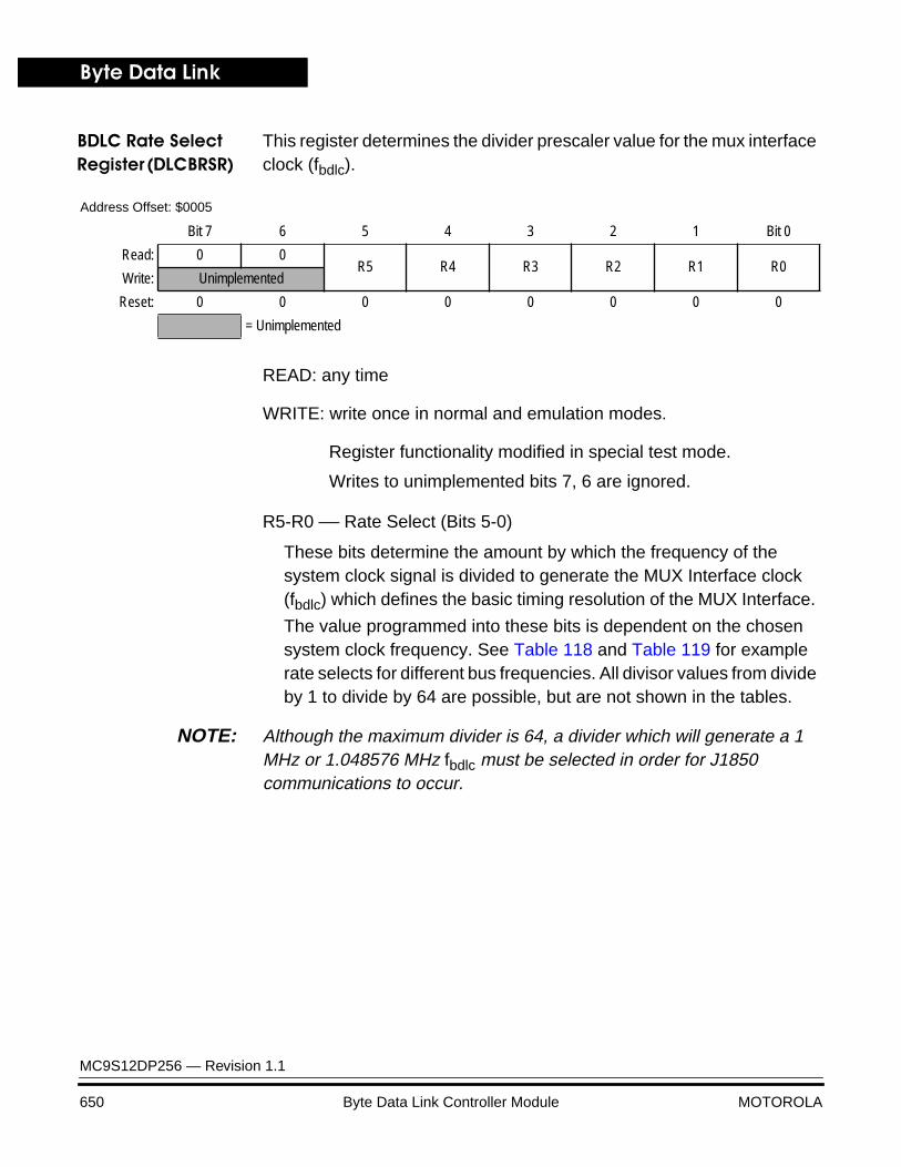
Byte Data Link
MC9S12DP256 — Revision 1.1
650 Byte Data Link Controller Module MOTOROLA
BDLC Rate Select Register (DLCBRSR)
This register determines the divider prescaler value for the mux interface clock (fbdlc).
READ: any time
WRITE: write once in normal and emulation modes.
Register functionality modified in special test mode.
Writes to unimplemented bits 7, 6 are ignored.
R5-R0 — Rate Select (Bits 5-0)
These bits determine the amount by which the frequency of the system clock signal is divided to generate the MUX Interface clock (fbdlc) which defines the basic timing resolution of the MUX Interface.
The value programmed into these bits is dependent on the chosen system clock frequency. See Table 118 and Table 119 for example rate selects for different bus frequencies. All divisor values from divide by 1 to divide by 64 are possible, but are not shown in the tables.
NOTE: Although the maximum divider is 64, a divider which will generate a 1 MHz or 1.048576 MHz fbdlc must be selected in order for J1850 communications to occur.
Address Offset: $0005
Bit 7 6 5 4 3 2 1 Bit 0
Read: 0 0R5 R4 R3 R2 R1 R0
Write: Unimplemented
Reset: 0 0 0 0 0 0 0 0
= Unimplemented
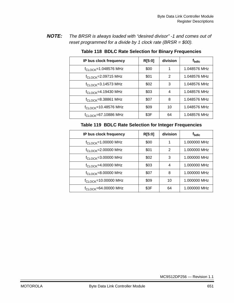
Byte Data Link Controller ModuleRegister Descriptions
MC9S12DP256 — Revision 1.1
MOTOROLA Byte Data Link Controller Module 651
NOTE: The BRSR is always loaded with “desired divisor” -1 and comes out of reset programmed for a divide by 1 clock rate (BRSR = $00).
Table 118 BDLC Rate Selection for Binary Frequencies
IP bus clock frequency R[5:0] division fbdlc
fCLOCK=1.048576 MHz $00 1 1.048576 MHz
fCLOCK=2.09715 MHz $01 2 1.048576 MHz
fCLOCK=3.14573 MHz $02 3 1.048576 MHz
fCLOCK=4.19430 MHz $03 4 1.048576 MHz
fCLOCK=8.38861 MHz $07 8 1.048576 MHz
fCLOCK=10.48576 MHz $09 10 1.048576 MHz
fCLOCK=67.10886 MHz $3F 64 1.048576 MHz
Table 119 BDLC Rate Selection for Integer Frequencies
IP bus clock frequency R[5:0] division fbdlc
fCLOCK=1.00000 MHz $00 1 1.000000 MHz
fCLOCK=2.00000 MHz $01 2 1.000000 MHz
fCLOCK=3.00000 MHz $02 3 1.000000 MHz
fCLOCK=4.00000 MHz $03 4 1.000000 MHz
fCLOCK=8.00000 MHz $07 8 1.000000 MHz
fCLOCK=10.00000 MHz $09 10 1.000000 MHz
fCLOCK=64.00000 MHz $3F 64 1.000000 MHz
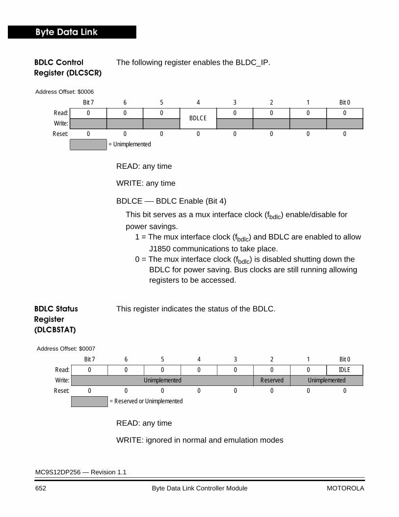
Byte Data Link
MC9S12DP256 — Revision 1.1
652 Byte Data Link Controller Module MOTOROLA
BDLC Control Register (DLCSCR)
The following register enables the BLDC_IP.
READ: any time
WRITE: any time
BDLCE — BDLC Enable (Bit 4)
This bit serves as a mux interface clock (fbdlc) enable/disable for
power savings.1 = The mux interface clock (fbdlc) and BDLC are enabled to allow
J1850 communications to take place.0 = The mux interface clock (fbdlc) is disabled shutting down the
BDLC for power saving. Bus clocks are still running allowing registers to be accessed.
BDLC Status Register (DLCBSTAT)
This register indicates the status of the BDLC.
READ: any time
WRITE: ignored in normal and emulation modes
Address Offset: $0006
Bit 7 6 5 4 3 2 1 Bit 0
Read: 0 0 0BDLCE
0 0 0 0
Write:
Reset: 0 0 0 0 0 0 0 0
= Unimplemented
Address Offset: $0007
Bit 7 6 5 4 3 2 1 Bit 0
Read: 0 0 0 0 0 0 0 IDLE
Write: Unimplemented Reserved Unimplemented
Reset: 0 0 0 0 0 0 0 0
= Reserved or Unimplemented
Byte Data Link Controller ModuleExternal Pin Descriptions
MC9S12DP256 — Revision 1.1
MOTOROLA Byte Data Link Controller Module 653
Register functionality is modified in special test mode.
IDLE Idle (Bit 0)
This bit indicates when the BDLC is idle.1 = BDLC has received IFS and no data is being transmitted or
received.0 = BDLC is either transmitting or receiving data.
NOTE: BDLC is only idle after receiving IFS. The IDLE bit is 0 during reset since the BDLC needs to wait for an IFS before becoming idle. Noise on the bus will be filtered and the IDLE bit will remain unchanged.
External Pin Descriptions
The BDLC module has a control bit, BDLCE, for two external pins, PM0 and PM1. The BDLCE bit enables and disables the BDLC and its J1850 functions. The transmit pin (Txp) function is multiplexed on the PM1 port and the receive pin (Rxp) function is multiplexed on the PM0 port. The BDLC pins are shared with the CAN0 pins. When the BDLC is enabled, the BDLC function takes control of these two shared pins.
NOTE: If both BDLC and CAN0 are enabled, the CAN0 will take control of these two pins and no BDLC function will occur on these pins.
Reset Initialization/Basic Operation
The reset state of each individual bit is listed within the Register Descriptions section Register Descriptions which details the registers and their bit-fields.
This section includes sample flows for initializing the BDLC and using it to transmit and receive messages.
Initialization Sequence
To initialize the BDLC, the user should first write the desired data to the configuration bits. The BDLC should then be taken out of digital and analog loopback mode and enabled. Exiting from loopback mode will
Byte Data Link
MC9S12DP256 — Revision 1.1
654 Byte Data Link Controller Module MOTOROLA
entail change of state indications in the DLCBSVR which must be dealt with. Once this is complete, CPU interrupts can be enabled (if desired), and then the BDLC module is capable of SAE J1850 serial network communication. For an illustration of the sequence necessary for initializing the BDLC, refer to Figure 128.
Initializing the Configuration Bits
The first step necessary for initializing the BDLC following an MCU reset is to write the desired values to each of the BDLC control registers. This is best done by storing predetermined initialization values directly into these registers. The following description outlines a basic flow for initializing the BDLC. This basic flow does not detail more elaborate initialization routines, such as performing digital and analog loopback tests before enabling the BDLC for SAE J1850 communication. However, from the following descriptions and the BDLC specification, the user should be able to develop routines for performing various diagnostic procedures such as loopback tests.
Step 1 - Initialize DLCBARD
Begin initialization of the configuration bits by writing the desired analog transceiver configuration data into the DLCBARD register. Following this write to DLCBARD, all of these bits will become read only.
Step 2- Initialize DLCBRSR
The next step in BDLC initialization is to write the desired bus clock divisor minus one into the DLCBRSR register. The divisor should be chosen to generate a 1 MHz or 1.048576 MHz mux interface clock (fbdlc). Following this write to DLCBRSR, all of these bits will become read only.
Step 3- Initialize DLCBCR2
The next step in BDLC initialization should be writing the configuration bits into the DLCBCR2 register. This initialization description assumes that the BDLC will be put into normal mode (not 4X mode), and that the BDLC should not yet exit either digital or analog loopback mode. Therefore, this step should write SMRST and DLOOP as logic ones, RX4XE as a logic zero, write NBFS to the desired level, and write TEOD, TSIFR, TMIFR1 and TMIFR0 as logic zeros. These last four bits MUST be written as logic zeros in order to prevent undesired operation of the BDLC.
Byte Data Link Controller ModuleReset Initialization/Basic Operation
MC9S12DP256 — Revision 1.1
MOTOROLA Byte Data Link Controller Module 655
Step 4- Initialize DLCBCR1
The next step in BDLC initialization is to write the configuration bits in DLCBCR1. The CLKS bit should be written to its desired values at this time, following which it will become read-only. The IE bit should be written as a logic zero at this time so BDLC interrupts of the CPU will remain masked for the time being. The IMSG bit should be written as a logic one to prevent any receive events from setting the DLCBSVR until a valid SOF (or BREAK) symbol has been received by the BDLC.
Exiting Loopback Mode and Enabling the BDLC
Once the configuration bits have been written to the desired values, the BDLC should be taken out of loopback and connected to the SAE J1850 bus. This is done by clearing the DLOOP bit and then setting the BDLCE bit in the DLCSCR.
Step 5- Perform Loopback Tests (optional)
Once the BDLC is configured for desired operation, the user may wish to perform digital and/or analog loopback tests to determine the integrity of the link to the SAE J1850 network. This would involve leaving the DLOOP bit (DLCBCR2) set, setting the BDLCE bit, preforming the desired loopback tests and finally exiting digital loopback mode by clearing DLOOP in the DLCBCR2.
Step 6- Exit Loopback Mode and enable the BDLC
If loopback mode tests are not to be preformed the BDLC can be removed from digital loopback mode by clearing the DLOOP bit. The BDLC can then be enabled by setting the BDLCE bit in the DLCSCR.
Once DLOOP is cleared and BDLCE is set, the BDLC is ready for SAE J1850 communication. However, to ensure that the BDLC does not attempt to receive a message already in progress or to transmit a message while another device is transmitting, the BDLC must first observe an EOF symbol on the bus before the receiver will be activated. To activate the transmitter, the BDLC will need to observe an Inter-Frame Separator symbol.
Enabling BDLC Interrupts
The final step in readying the BDLC for proper communication is to clear any pending interrupt sources and then, if desired, enable BDLC interrupts of the CPU.
Byte Data Link
MC9S12DP256 — Revision 1.1
656 Byte Data Link Controller Module MOTOROLA
Step 7- Clear Pending BDLC Interrupts
In order to ensure that the BDLC does not immediately generate a CPU interrupt when interrupts are enabled, the user should read the DLCBSVR to determine if any BDLC interrupt sources are pending before setting the IE bit in the BCR1. If the BSVR reads as a%00000000, no interrupts are pending and the user is free to enable BDLC interrupts, if desired.
If the DLCBSVR indicates that an interrupt is pending, the user should perform whatever actions are necessary to clear the interrupt source before enabling the interrupts. Whether any interrupts are pending will depend primarily upon how much time passes between the exit from loopback modes and enabling the BDLC and the enabling of interrupts. It is a good practice to always clear any source of interrupts before enabling interrupts on any MCU subsystem.
If any interrupts are pending (DLCBSVR ≠ %00000000), then each interrupt source should be dealt with accordingly. Once all of the interrupt sources have been dealt with, the DLCBSVR should read%00000000, and the user is then free to enable BDLC interrupts.
Step 8- Enable BDLC Interrupts
The last step in initializing the BDLC module is to enable interrupts to the CPU, if so desired. This is done by simply setting the IE bit in the DLCBCR1. Following this, the BDLC module is ready for operating in interrupt mode. If the user chooses not to enable interrupts, the DLCBSVR must be polled periodically to ensure that state changes in the BDLC are detected and dealt with appropriately.
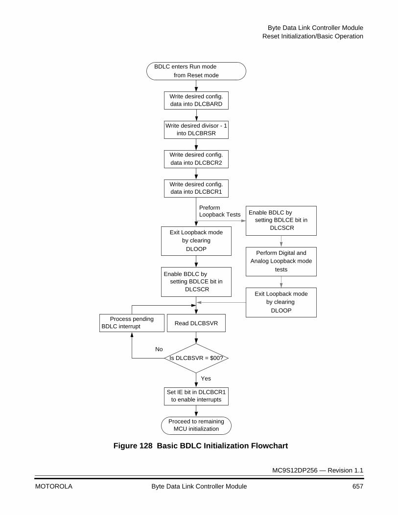
Byte Data Link Controller ModuleReset Initialization/Basic Operation
MC9S12DP256 — Revision 1.1
MOTOROLA Byte Data Link Controller Module 657
BDLC enters Run mode
from Reset mode
Write desired config.data into DLCBARD
Write desired config.data into DLCBCR1
Read DLCBSVR
Write desired config.data into DLCBCR2
Set IE bit in DLCBCR1to enable interrupts
Proceed to remainingMCU initialization
Figure 128 Basic BDLC Initialization Flowchart
Is DLCBSVR = $00?
Yes
No
Process pendingBDLC interrupt
Perform Digital andAnalog Loopback mode
tests
Exit Loopback modeby clearing
DLOOP
Enable BDLC bysetting BDLCE bit in
DLCSCR
PreformLoopback Tests
Exit Loopback modeby clearing
DLOOP
Enable BDLC bysetting BDLCE bit in
DLCSCR
Write desired divisor - 1into DLCBRSR
Byte Data Link
MC9S12DP256 — Revision 1.1
658 Byte Data Link Controller Module MOTOROLA
Transmitting A Message
The design of the BDLC module enables the user to easily handle message reception and message transmission separately. This can greatly simplify the communication software, as all received messages can be handled virtually the same, regardless of their origin.
This chapter will therefore describe only the steps necessary for transmitting a message, and will not address the resulting reception of that message by the BDLC. Message reception is described in Receiving A Message. Later sections will deal with transmitting and receiving In-Frame Responses on the SAE J1850 bus.
BDLC Transmission Control Bits
There is only one BDLC control bit which is used when transmitting a message onto the SAE J1850 bus. This bit, the Transmit End of Data (TEOD) bit, is set by the user to indicate to the BDLC that the last byte of that part of the message frame has been loaded into the DLCBDR. The TEOD bit, located in DLCBCR2, is also used when transmitting an In-Frame Response (IFR), but that usage is described in Transmitting An In-Frame Response (IFR). Setting the TEOD bit indicates to the BDLC that the last byte written to the BDLC Data Register is the final byte to be transmitted, and that following this byte a CRC byte and EOD symbol should be transmitted automatically. Setting the TEOD bit will also inhibit any further TDRE interrupts until TEOD is cleared. The TEOD bit will be cleared on the rising edge of the first bit of the transmitted CRC byte, or if an error or loss of arbitration is detected on the bus.
BDLC Data Register
The BDLC Data Register is a double-buffered register which is used for handling the transmitted and received message bytes.Bytes to be transmitted onto the SAE J1850 bus are written to the DLCBDR, and bytes received from the bus by the BDLC are read from the DLCBDR. Since this register is double buffered, bytes written into it cannot be read by the CPU. If this is attempted, the byte which is read will be the last byte placed in the DLCBDR by the BDLC, not the last byte written to the
Byte Data Link Controller ModuleTransmitting A Message
MC9S12DP256 — Revision 1.1
MOTOROLA Byte Data Link Controller Module 659
DLCBDR by the CPU. For an illustration of the DLCBDR, refer to BDLC Data Register (DLCBDR).
Transmitting a Message with the BDLC
To transmit a message using the BDLC, the user just writes the first byte of the message to be transmitted into the DLCBDR, initiating the transmission process. When the TDRE status appears in the DLCBSVR, the user writes the next byte into the DLCBDR. Once all of the bytes have been loaded into the DLCBDR, the user sets the TEOD bit, and the BDLC completes the message transmission. What follows is an overview of the basic steps required to transmit a message onto an SAE J1850 network using the BDLC. For an illustration of this sequence, refer to Basic BDLC Transmit Flowchart.
NOTE: Due to the byte-level architecture of the BDLC module, the 12-byte limit on message length as defined in SAE J1850 must be enforced by the user’s software. The number of bytes in a message (transmitted or received) has no meaning to the BDLC.
Step 1: Write the First Byte into the DLCBDR
To initiate a message transmission, the CPU simply loads the first byte of the message to be transmitted into the DLCBDR. The BDLC will then perform the necessary bus acquisition duties to determine when the message transmission can begin.
Once the BDLC determines that the SAE J1850 bus is free, a Start of Frame (SOF) symbol will be transmitted, followed by the byte written to the DLCBDR. Once the BDLC readies this byte for transmission, the DLCBSVR will reflect that the next byte can be written to the DLCBDR (TDRE interrupt).
NOTE: If the user writes the first byte of a message to be transmitted to the DLCBDR and then determines that a different message should be transmitted, the user can write a new byte to the DLCBDR up until the transmission begins. This new byte will replace the original byte in the DLCBDR.
Byte Data Link
MC9S12DP256 — Revision 1.1
660 Byte Data Link Controller Module MOTOROLA
Step 2: When TDRE is Indicated, Write the Next Byte into the DLCBDR
When a TDRE state is reflected in the BSVR, the CPU writes the next byte to be transmitted into the BDR. This step is repeated until the last byte to be transmitted is written to the DLCBDR.
NOTE: Due to the design and operation of the BDLC, when transmitting a message the user may write two, or possibly even three of the bytes to be transmitted into the DLCBDR before the first RDRF interrupt occurs. For this reason, the user should never use receive interrupts to control the sequencing of bytes to be transmitted.
Step 3: Write the Last Byte to the DLCBDR and Set TEOD
Once the user has written the last byte to be transmitted into the DLCBDR, the user then sets the TEOD bit in DLCBCR2. When the TEOD bit is set, once the byte written to the DLCBDR is transmitted onto the bus, the BDLC will begin transmitting the 8-bit CRC byte, as specified in SAE J1850. Following the CRC byte, the BDLC will transmit an EOD symbol onto the SAE J1850 bus, indicating that this part of the message has been completed. If no IFR bytes are transmitted following the EOD, an EOF will be recognized and the message will be complete.
Setting the TEOD bit is the last step the CPU needs to take to complete the message transmission, and no further transmission-related interrupts will occur. Once the message has been completely received by the BDLC, an EOF interrupt will be generated. However, this is technically a receive function which can be handled by the message reception routine.
NOTE: While the TEOD bit is typically set immediately following the write of the last byte to the BDR, it is also acceptable to wait until a TDRE interrupt is generated before setting the TEOD bit. While the example flowchart in Figure 129 shows the TEOD bit being set after the write to the BDR, either method is correct. If a TDRE interrupt is pending, it will be cleared when the TEOD bit is set.
Transmitting Exceptions
While this is the basic transmit flow, at times the message transmit process will be interrupted. This can be due to a loss of arbitration to a higher priority message or due to an error being detected on the
Byte Data Link Controller ModuleTransmitting A Message
MC9S12DP256 — Revision 1.1
MOTOROLA Byte Data Link Controller Module 661
network. For the transmit routine, either of these events can be dealt with in a similar manner.
Loss of Arbitration If a loss of arbitration (LOA) occurs while the BDLC is transmitting onto the SAE J1850 bus, the BDLC will immediately stop transmitting, and a LOA status will be reflected in the DLCBSVR. If the loss of arbitration has occurred on a byte boundary, an RDRF interrupt may also be pending once the LOA interrupt is cleared.
When a loss of arbitration occurs, the J1850 message handling software should immediately switch into the receive mode. If the TEOD bit was set, it will be cleared automatically. If another attempt is to be made to transmit the same message, the user must start the transmit sequence over from the beginning of the message.
Error Detection Similar to a loss of arbitration, if any error (except a CRC error) is detected on the SAE J1850 bus during a transmission, the BDLC will stop transmitting immediately. The byte which was being transmitted will be discarded, and the “Symbol Invalid or Out of Range” status will be reflected in the DLCBSVR. As with the loss of arbitration, if the TEOD bit was set, it will be cleared automatically, and any attempt to transmit the same message will have to start from the beginning.
If a CRC error occurs following a transmission, this will also be reflected in the DLCBSVR. However, since the CRC error is really a receive error based on the received CRC byte, at this point all bytes of the message will have been transmitted. It is therefore up to the user’s software to determine if another attempt should be made to transmit the message in which the error occurred.
Transmitter Underrun
A transmitter underrun can occur when a TDRE interrupt is not serviced in a timely fashion. If the last byte loaded into the DLCBDR is completely transmitted onto the network before the next byte is loaded into the BDR, a transmitter underrun will occur. If this does happen, the BDLC will transmit two additional logic ones to ensure that the partial message which was transmitted onto the bus does not end on a byte boundary. This will be followed by an EOD and EOF symbol. The only indication to the CPU that an underrun occurred is the Symbol Invalid or Out of Range

Byte Data Link
MC9S12DP256 — Revision 1.1
662 Byte Data Link Controller Module MOTOROLA
error which will be indicated in the DLCBSVR. As with the other errors, it is up to the user’s software to determine if another transmission attempt should be made.
In-Frame Response to a Transmitted Message
If an In-Frame Response (IFR) is received following the transmission of a message, the status indicating that an IFR byte has been received will be indicated in the DLCBSVR before an EOF is indicated. Refer to Receiving An In-Frame Response (IFR) for a description of how to handle the reception of IFR bytes.
Aborting a Transmission
The BDLC module does not have a mechanism designed specifically for aborting a transmission. Since the module transmits each message on a byte-by-byte basis, there is little need to implement an abort mechanism. If the user has loaded a byte into the DLCBDR to initiate a message transmission and decides to send a different message, the byte in the DLCBDR can be replaced, right up to the point that the message transmission begins.
If the user has loaded a byte into the DLCBDR and then decides not to send any message at all, the user can let the byte transmit, and when the TDRE interrupt occurs let the transmitter underrun. This will cause two extra logic ones followed by an EOF to be transmitted. While this method may require a small amount of bus bandwidth, the need to do this should be very rare. Replacing the byte originally written to the BDR with $FF will also increase the probability of the transmitter losing arbitration if another node begins transmitting at the same time, also reducing the bus bandwidth needed.
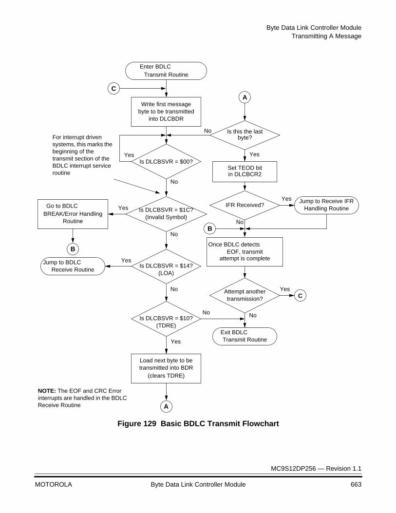
Byte Data Link Controller ModuleTransmitting A Message
MC9S12DP256 — Revision 1.1
MOTOROLA Byte Data Link Controller Module 663
Figure 129 Basic BDLC Transmit Flowchart
Enter BDLCTransmit Routine
Write first messagebyte to be transmitted
into DLCBDR
Is DLCBSVR = $00?Yes
No
Load next byte to betransmitted into BDR
(clears TDRE)
Is DLCBSVR = $1C?Yes
No
Is DLCBSVR = $14?Yes
No
Is DLCBSVR = $10?
Yes
No
(TDRE)
(LOA)
(Invalid Symbol)
Attempt another Yes
No
transmission?
Is this the last
Yes
Nobyte?
Jump to BDLCReceive Routine
Once BDLC detectsEOF, transmit
Set TEOD bitin DLCBCR2
attempt is complete
Yes
No
IFR Received?Jump to Receive IFR
Handling Routine
Exit BDLCTransmit Routine
Go to BDLCBREAK/Error Handling
Routine
For interrupt driven systems, this marks the beginning of the transmit section of the BDLC interrupt service routine
NOTE: The EOF and CRC Error interrupts are handled in the BDLC Receive Routine
CA
B
C
A
B
Byte Data Link
MC9S12DP256 — Revision 1.1
664 Byte Data Link Controller Module MOTOROLA
Receiving A Message
The design of the BDLC makes it especially easy to use for receiving messages off of the SAE J1850 bus. When the first byte of a message comes in, the DLCBSVR will indicate to the CPU that a byte has been received. As each successive byte is received, that will in turn be reflected in the DLCBSVR. When the message is complete and the EOF has been detected on the bus, the DLCBSVR will reflect this, indicating that the message is complete.
The basic steps required for receiving a message from the SAE J1850 bus are outlined below. For more information on receiving IFR bytes, refer to Receiving An In-Frame Response (IFR).
BDLC Reception Control Bits
The only control bit which is used for message reception, the IMSG bit, is actually used to prevent message reception. As described in IMSG — Ignore Message (Bit 7), when the IMSG bit is set BDLC interrupts of the CPU are inhibited until the next SOF symbol is received. This allows the BDLC to ignore the remainder of a message once the CPU has determined that it is of no interest. This helps reduce the amount of CPU overhead used to service messages received from the SAE J1850 network, since otherwise the BDLC would require attention from the CPU for each byte broadcast on the network. The IMSG bit is cleared when the BDLC receives an SOF symbol, or it can also be cleared by the CPU.
NOTE: While the IMSG bit can be used to prevent the CPU from having to service the BDLC for every byte transmitted on the SAE J1850 bus, the IMSG bit should never be used to ignore the BDLC’s own transmission. Because setting the IMSG bit prevents all DLCBSVR bits from being updated until an SOF is received, the user would not receive any further transmit-related interrupts until another SOF was received, making it very difficult for the CPU to complete the transmission correctly.

Byte Data Link Controller ModuleReceiving A Message
MC9S12DP256 — Revision 1.1
MOTOROLA Byte Data Link Controller Module 665
Receiving a Message with the BDLC
Receiving a message using the BDLC is extremely straight-forward. As each byte of a message is received and placed into the DLCBDR, the BDLC will indicate this to the CPU with an Rx Data Register Full (RDRF) status in the DLCBSVR. When an EOF symbol is received, indicating to the CPU that the message is complete, this too will be reflected in the DLCBSVR.
Outlined below are the basic steps to be followed for receiving a message from the SAE J1850 bus with the BDLC. For an illustration of this sequence, refer to Basic BDLC Receive Flowchart.
Step 1: When RDRF Interrupt Occurs, Retrieve Data Byte
When the first byte of a message following a valid SOF symbol is received that byte is placed in the DLCBDR, and an RDRF state is reflected in the DLCBSVR. No indication of the SOF reception is made, since the end of the previous message is marked by an EOF indication. The first RDRF state following this EOF indication should allow the user to determine when a new message begins.
The RDRF interrupt is cleared when the received byte is read from the DLCBDR. Once this is done, no further CPU intervention is necessary until the next byte is received, and this step is repeated.
All bytes of the message, including the CRC byte, will be placed into the DLCBDR as they are received for the CPU to retrieve.
Step 2: When an EOF is Received, the Message is Complete
Once all bytes (including the CRC byte) have been received from the bus, the bus will be idle for a time period equal to an EOD symbol. Once the EOD symbol is received, the BDLC will verify that the CRC byte is correct. If the CRC byte is not correct, this will be reflected in the DLCBSVR.
If no In-Frame Response bytes are transmitted following the EOD symbol, the EOD will transition into an EOF symbol. When the EOF is received it will be reflected in the DLCBSVR, indicating to the user that the message is complete. If IFR bytes do follow the first EOD symbol, once they are complete another EOD will be transmitted, followed by an EOF.
Byte Data Link
MC9S12DP256 — Revision 1.1
666 Byte Data Link Controller Module MOTOROLA
Once the EOF state is reflected in the DLCBSVR, this indicates to the user that the message is complete, and that when another byte is received it is the first byte of a new message.
Filtering Received Messages
No message filtering hardware is included on the BDLC, so all message filtering functions must be performed in software. Because the BDLC handles each message on a byte-by-byte basis, message filtering can be done as each byte is received, rather than after the entire message is complete. This enables the CPU to decide while a message is still in progress whether or not that message is of any interest.
At any point during a message, if the CPU determines that the message is of no interest the IMSG bit can be set. Setting the IMSG bit commands the BDLC not to update the DLCBSVR until the next valid SOF is received. This prevents the CPU from having to service the BDLC for each byte of every message sent over the network.
Receiving Exceptions
As with a message transmission, this basic message reception flow can be interrupted if errors are detected by the BDLC. This can occur if an incorrect CRC is detected or if an invalid or out of range symbol appears on the SAE J1850 bus. A problem can also arise if the CPU fails to service the DLCBDR in a timely manner during a message reception.
Receiver Overrun Once a message byte has been received, the CPU must service the DLCBDR before the next byte is received, or the first byte will be lost. If the DLCBDR is not serviced quickly enough, the next byte received will be written over the previous byte in the DLCBDR. No receiver overrun indication is made to the CPU. If the CPU fails to service the BDLC during the reception of an entire message, the byte remaining in the DLCBDR will be last byte received (usually a CRC byte).
Once a receiver overrun occurs, there is no way for the CPU to recover the lost byte(s), so the entire message should be discarded. To prevent receiver overrun, the user should ensure that a BDLC RDRF interrupt will be serviced before the next byte can be received. When polling the DLCBSVR, the user should select a polling interval which will provide timely monitoring of the BDLC.
Byte Data Link Controller ModuleReceiving A Message
MC9S12DP256 — Revision 1.1
MOTOROLA Byte Data Link Controller Module 667
CRC Error If a CRC error is detected during a message reception, this will be reflected in the BSVR once an EOD time is recognized by the BDLC. Since all bytes of the message will have been received when this error is detected, it is up to the user to ensure that all the received message bytes are discarded.
Invalid or Out of Range Symbol
If an invalid or out of range symbol, a framing error or a BREAK symbol is detected on the SAE J1850 bus during the reception of a message, the BDLC will immediately stop receiving the message and discard any partially received byte. The “Symbol Invalid or Out of Range” status will immediately be reflected in the DLCBSVR. Following this the BDLC will wait until the bus has been idle for a time period equal to an EOF symbol before receiving another message. As with the CRC error, the user should discard any partially received message if this occurs.
In-Frame Response to a Received Message
As mentioned above, if one or more IFR bytes are received following the reception of a message, the status indicating the reception of the IFR byte(s) will be indicated in the DLCBSVR before the EOF is indicated. Refer to Receiving An In-Frame Response (IFR) for a description of how to deal with the reception of IFR bytes.

Byte Data Link
MC9S12DP256 — Revision 1.1
668 Byte Data Link Controller Module MOTOROLA
Figure 130 Basic BDLC Receive Flowchart
Enter BDLC
Is DLCBSVR
No
Store received byte(in case of LOA)
Is this messageYes
No
Is this an IFRYes
No
Is DLCBSVR = $04?
No
Yes
(EOF)
reception?
of any interest?
Is this a transmit
Yes
No
reflection?
Yes
Jump to Receive IFRHandling Routine
Once BDLC Detects
Go to BDLCBREAK/Error Handling
reception is complete
Yes
No
Is DLCBSVR
Jump to Transmit IFRHandling Routine
Exit BDLCReceive Routine
Routine(Error Detected)
(RDRF)Read byte in DLCBDR
Filter received byte
Set IMSG bit in DLCBCR1Store received byte
Is an IFR toYes
No
be transmitted?
Receive Routine
EOF, message
= $1C/$18?
= $0C?
B
B
B
A
A
Byte Data Link Controller ModuleTransmitting An In-Frame Response (IFR)
MC9S12DP256 — Revision 1.1
MOTOROLA Byte Data Link Controller Module 669
Transmitting An In-Frame Response (IFR)
The BDLC can be used to transmit all four types of In-Frame Response (IFR) which are defined in SAE J1850. A very brief definition of each IFR type is given below. For a more detailed description of each, refer the SAE J1850 document.
The explanation regarding IFR support by the BDLC which assumes the user is familiar with the use of IFRs as defined in SAE J1850, and understands the message header bit encoding and normalization bit formats which are used with the different types of IFRs. For more information on this, refer to the SAE J1850 document.
IFR Types Supported by the BDLC
SAE J1850 defines four distinct types of IFR. The first (and most basic) IFR is Type 0, or no IFR. IFR types 1, 2 & 3 are each made up of one or more bytes and, depending upon the type used, may be followed by a CRC byte. The BDLC is designed to allow the user to transmit and receive all types of SAE J1850 IFRs, but only the network framing/error checking/bus acquisition duties are performed by the BDLC. The user is responsible for determining the type of IFR to be transmitted, the number of retries to be made (if allowed), and the allowable number of bytes to be transmitted.
IFR Type 0: No Response
The most basic type of IFR is no IFR. The Type 0 IFR, as defined in SAE J1850, is no response. The EOD and EOF symbols follow directly after the CRC byte at the end of the message frame being transmitted. This type of IFR is, of course, inherently supported by the BDLC with no additional user intervention required.
IFR Type 1: Single Byte from a Single Responder
SAE J1850 defines the Type 1 IFR as a single byte from a single receiver. This type of IFR is used to acknowledge to the transmitter that the message frame was transmitted successfully on the network, and that at least one receiver received it correctly. A Type 1 IFR generally consists of the physical node ID of the receiver responding to the message, with no CRC byte appended. This type of response is used for Broadcast-type messages, where there may be several intended
Byte Data Link
MC9S12DP256 — Revision 1.1
670 Byte Data Link Controller Module MOTOROLA
receivers for a message but the transmitter only wants to know that at least one node received it. In this case, all receivers will begin transmitting their node ID following the EOD. Since all nodes on an SAE J1850 network have a unique node ID, if multiple nodes begin transmitting their node ID simultaneously, arbitration takes place. The node with the highest priority (lowest value) ID wins this arbitration process, and that node’s ID makes up the IFR. No retries are attempted by the nodes which lose arbitration during a Type 1 IFR transmission.
A Type 1 IFR can also be used as a response to a physically addressed message, where the only intended receiver is the one which responds. In this case, no arbitration would take place during the IFR transmission, but the resulting IFR would still consist of a single byte.
IFR Type 2: Single Byte from Multiple Responders
The Type 2 IFR, as defined in SAE J1850, is a series of single bytes, each transmitted by a different responder. This IFR type not only acknowledges to the transmitter that the message was transmitted successfully, but also reveals which receivers actually received the message. As with the Type 1 IFR, no CRC byte is appended to the end of a Type 2 IFR.
This IFR type is typically used with Function-type messages, where the original transmitter may need to know which nodes actually received the message. The basic difference between this type of IFR and the Type 1 IFR is that the nodes which lose arbitration while attempting to transmit their node ID during a Type 2 IFR wait until the byte which wins arbitration is transmitted and then again attempt to transmit their node ID onto the bus. The result is a series of node IDs, one from each receiver of the original message.
IFR Type 3: Multiple Bytes from a Single Responder
The last type of IFR defined by SAE J1850 is the Type 3 IFR. This IFR type consists of one or more bytes from a single responder. This type of IFR is used to return data to the original transmitter within the original message frame. This type of IFR may or may not have a CRC byte appended to it.
The Type 3 IFR is typically used with Function Read-type or Function Query-type messages, where the original transmitter is requesting data from the intended receiver. The node requesting the data transmits the
Byte Data Link Controller ModuleTransmitting An In-Frame Response (IFR)
MC9S12DP256 — Revision 1.1
MOTOROLA Byte Data Link Controller Module 671
initial portion of the message, and the intended receiver responds by transmitting the desired data in an IFR. In most cases, the original message requiring a Type 3 IFR is addressed to one particular node, so no arbitration should take place during the IFR portion of the message.
BDLC IFR Transmit Control Bits
The BDLC has three bits which are used to control the transmission of an In-Frame Response. These bits, all located in DLCBCR2, are TSIFR, TMIFR1 and TMIFR0. Each is used in conjunction with the TEOD bit to transmit one of three IFR types defined in SAE J1850. What follows is a brief description of each bit.
Because each of the bits used for transmitting an IFR with the BDLC is used to transmit a particular type of IFR, only one bit should be set by the CPU at a time. However, should more than one of these bits get set at one time, a priority encoding scheme is used to determine which type of IFR is sent. This scheme prevents unpredictable operation caused by conflicting signals to the BDLC. Table 120 illustrates which IFR bit will actually be acted upon by the BDLC should multiple IFR bits get set at the same time.
NOTE: As with transmitted messages, IFRs transmitted by the BDLC will also be received by the BDLC. For a description of how IFR bytes received by the BDLC should be handled, refer to Receiving An In-Frame Response (IFR).
Table 120 IFR Control Bit Priority Encoding
Read/Write Actual
TSIFR TMIFR1 TMIFR0 TSIFR TMIFR1 TMIFR0
0 0 0 0 0 0
1 X X 1 0 0
0 1 X 0 1 0
0 0 1 0 0 1
Byte Data Link
MC9S12DP256 — Revision 1.1
672 Byte Data Link Controller Module MOTOROLA
Transmit Single Byte IFR
The Transmit Single Byte IFR (TSIFR) bit in DLCBCR2 is used to transmit Type 1 and Type 2 IFRs onto the SAE J1850 bus. If this bit is set after a byte is loaded into the BDR, the BDLC will attempt to send that byte, preceded by the appropriate Normalization Bit, as a single byte IFR without a CRC. If arbitration is lost, the BDLC will automatically attempt to transmit the byte again (without a Normalization Bit) as soon as the byte winning arbitration completes transmission. Attempts to transmit the byte will continue until either the byte is successfully transmitted, the TEOD bit is set by the user or an error is detected on the bus.
The user must set the TSIFR bit before the EOD following the main part of the message frame is received, or no IFR transmit attempts will be made for the current message. If another node does transmit an IFR to this message or a reception error occurs, the TSIFR bit will be cleared. If not, the IFR will be transmitted after the EOD of the next received message.
The TSIFR bit will be automatically cleared once the EOD following one or more IFR bytes has been received or an error is detected on the bus.
Transmit Multi-Byte IFR 1
The Transmit Multi-Byte IFR 1 (TMIFR1) bit is used to transmit an SAE J1850 Type 3 IFR with a CRC byte appended. If this bit is set after the user has loaded the first byte of a multi-byte IFR into the DLCBDR, the BDLC will begin transmitting that byte, preceded by the appropriate Normalization Bit, onto the SAE J1850 bus. Once this happens a TDRE interrupt will occur, indicating to the user that the next IFR byte should be loaded into the DLCBDR. When the last byte to be transmitted is written to the DLCBDR, the user sets the TEOD bit. This will cause a CRC byte and an EOD symbol to be transmitted following the last IFR byte.
As with the TSIFR bit, the TMIFR1 bit must be set before the EOD symbol is received, or it will remain cleared and no IFR transmit attempt will be made. The TMIFR1 bit will be cleared once the CRC byte and EOD are transmitted, if an error is detected on the bus, if a loss of arbitration occurs during the IFR transmission or if a transmitter underrun occurs when the user fails to service the TDRE interrupt in a
Byte Data Link Controller ModuleTransmitting An In-Frame Response (IFR)
MC9S12DP256 — Revision 1.1
MOTOROLA Byte Data Link Controller Module 673
timely manner. If a loss of arbitration occurs while the Type 3 IFR is being transmitted, transmission will halt immediately and the loss of arbitration will be indicated in the DLCBSVR.
Transmit Multi-Byte IFR 0
The Transmit Multi-Byte IFR 0 (TMIFR0) bit is used to transmit an SAE J1850 Type 3 IFR without a CRC byte appended. If this bit is set after the user has loaded the first byte of a multi-byte IFR into the DLCBDR, the BDLC will begin transmitting that byte, preceded by the appropriate Normalization Bit, onto the SAE J1850 bus. Once this happens a TDRE interrupt will occur, indicating to the user that the next IFR byte should be loaded into the DLCBDR. When the last byte to be transmitted is written to the DLCBDR, the user sets the TEOD bit. This will cause an EOD symbol to be transmitted following the last IFR byte.
As with the TSIFR and TMIFR1 bits, the TMIFR0 bit must be set before the EOD symbol is received, or it will remain cleared and no IFR transmit attempt will be made. The TMIFR0 bit will be cleared once the CRC byte and EOD are transmitted, if an error is detected on the bus, if a loss of arbitration occurs during the IFR transmission or if a transmitter underrun occurs when the user fails to service the TDRE interrupt in a timely manner. If a loss of arbitration occurs while the Type 3 IFR is being transmitted, transmission will halt immediately and the loss of arbitration will be indicated in the DLCBSVR.
NOTE: The TMIFR0 bit should not be used to transmit a Type 1 IFR. If a loss of arbitration occurs on the last bit of a byte being transmitted using the TMIFR0 bit, two extra logic ones will be transmitted to ensure that the IFR will not end on a byte boundary. This can cause an error in a Type 1 IFR.
Transmitting An IFR with the BDLC
While the design of the BDLC makes the transmission of each type of IFR similar, the steps necessary for sending each will be discussed. Again, a discussion of the bytes making up any particular IFR is not within the scope of this document. For a more detailed description of the use of IFRs on an SAE J1850 network, refer to the SAE J1850 document.
Byte Data Link
MC9S12DP256 — Revision 1.1
674 Byte Data Link Controller Module MOTOROLA
Transmitting a Type 1 IFR
To transmit a Type 1 IFR, the user loads the byte to be transmitted into the DLCBDR and sets both the TSIFR bit and the TEOD bit. This will direct the BDLC to attempt transmitting the byte written to the DLCBDR one time, preceded by the appropriate Normalization Bit. If the transmission is not successful, the byte will be discarded and no further transmission attempts will be made. For an illustration of the steps described below, refer to Transmitting A Type 1 IFR.
Step 1: Load the IFR Byte into the BDR
The user begins initiation of a Type 1 IFR by loading the desired IFR byte into the DLCBDR. If a byte has already been written into the DLCBDR for transmission as a new message, the user can simply write the IFR byte to the DLCBDR, replacing the previously written byte. This must be done before the first EOD symbol is received.
Step 2: Set the TSIFR and TEOD Bits
The final step in transmitting a Type 1 IFR with the BDLC is to set the TSIFR and TEOD bits in DLCBCR2. Setting both bits will direct the BDLC to make one attempt at transmitting the byte in the DLCBDR as an IFR. If the byte is transmitted successfully, or if an error or loss of arbitration occurs, TEOD and TSIFR will be cleared and no further transmit attempts will be made.
Transmitting a Type 2 IFR
To transmit a Type 2 IFR, the user loads the byte to be transmitted into the DLCBDR and sets the TSIFR bit. Once this is done, the BDLC will attempt to transmit the byte in the DLCBDR as a single byte IFR, preceded by the appropriate Normalization Bit. If the first BDLC loses arbitration on the first attempt, it will make repeated attempts to transmit this byte until it is successful, an error occurs or the user sets the TEOD bit.

Byte Data Link Controller ModuleTransmitting An In-Frame Response (IFR)
MC9S12DP256 — Revision 1.1
MOTOROLA Byte Data Link Controller Module 675
Step 1: Load the IFR Byte into the BDR
As with the Type 1 IFR, the user begins initiation of a Type 2 IFR by loading the desired IFR byte into the DLCBDR. If a byte has already been written into the DLCBDR for transmission as a new message, the user can simply write the IFR byte to the DLCBDR, replacing the previously written byte. This must be done before the first EOD symbol is received.
Figure 131 Transmitting A Type 1 IFR
Enter Type 1 IFRTransmit Routine
Is DLCBSVR = $1C?No
Yes
Load IFR byteinto DLCBDR
(Error Detected)
Set TSIFR and TEOD
Once BDLC detects,or EOF, IFR transmitattempt is complete
Is DLCBSVR = $14?
No
Yes
(LOA)
Exit Type 1 IFRTransmit Routine
Jump to Receive IFRHandling Routine
IFR byte is discarded
IFR byte is discarded
Load IFR byteinto DLCBDR
Byte Data Link
MC9S12DP256 — Revision 1.1
676 Byte Data Link Controller Module MOTOROLA
Step 2: Set the TSIFR Bit
The second step necessary for transmitting a Type 2 IFR is to set the TSIFR bit in DLCBCR2. Setting this bit will direct the BDLC to attempt to transmit the byte in the DLCBDR as an IFR until it is successful. If the byte is transmitted successfully, or if an error or loss of arbitration occurs, TSIFR will be cleared and no further transmit attempts will be made.
Step 3: If Necessary, Set the TEOD Bit
The third step in transmitting a Type 2 IFR is only necessary if the user wishes to halt the transmission attempts. This may be necessary if the BDLC’s attempt to transmit the byte loaded into the DLCBDR continually loses arbitration, and the overall message length approaches the 12-byte limit as defined in SAE J1850.
If it becomes necessary to halt the IFR transmission attempts, the user simply sets the TEOD bit in BCR2. If the BDLC is between transmission attempts, it will make one more attempt to transmit the IFR byte. If it is transmitting the byte when TEOD is set, the BDLC will continue the transmission until it is successful or it loses arbitration to another transmitter. At this point it will then discard the byte and make no more transmit attempts.
NOTE: When transmitting a Type 2 IFR, the user should monitor the number of IFR bytes received to ensure that the overall message length does not exceed the 12-byte limit for the length of SAE J1850 messages. The user should set the TEOD bit when the 11th byte is received, which will prevent the 12-byte limit from being exceeded.

Byte Data Link Controller ModuleTransmitting An In-Frame Response (IFR)
MC9S12DP256 — Revision 1.1
MOTOROLA Byte Data Link Controller Module 677
Transmitting a Type 3 IFR
Transmitting a Type 3 IFR, with or without a CRC byte, is done in a fashion similar to transmitting a message frame. The user loads the first byte to be transmitted into the DLCBDR and then sets the appropriate TMIFR bit, depending upon whether a CRC byte is desired. When the
Figure 132 Transmitting A Type 2 IFR
Enter Type 2 IFRTransmit Routine
Is DLCBSVR = $1C? No
Yes
Load IFR byteinto DLCBDR
(Error Detected)
Set TSIFR in DLCBCR2
Once BDLC detects,or EOF, IFR transmitattempt is complete
Is DLCBSVR = $14?
No
Yes
(LOA)
Exit Type 1 IFRTransmit Routine
Jump to Receive IFRHandling Routine
IFR byte is discarded IFR byte is discarded
Was this the last No
Yes
transmit attempt?Was the 11th No
Yes
msg byte received?
Set TEOD in DLCBCR2
Jump to Receive IFRHandling Routine
Byte Data Link
MC9S12DP256 — Revision 1.1
678 Byte Data Link Controller Module MOTOROLA
last byte is written to the BDR, the TEOD bit is set, and a CRC byte (if desired) and an EOD are then transmitted. Because the two versions of the Type 3 IFR are transmitted identically, the description which follows will discuss both. For an illustration of the Type 3 IFR transmit sequence, refer to Transmitting A Type 3 IFR.
Step 1: Load the First IFR Byte into the DLCBDR
The user begins initiation of a Type 3 IFR, as with each of the other IFR types, by loading the desired IFR byte into the DLCBDR. If a byte has already been written into the DLCBDR for transmission as a new message, the user can simply write the first IFR byte to the DLCBDR, replacing the previously written byte. This must be done before the first EOD symbol is received.
Step 2: Set the TMIFR Bit
The second step necessary for transmitting a Type 3 IFR is to set the desired TMIFR bit in DLCBCR2, depending upon whether or not a CRC is desired. As previously described in BDLC IFR Transmit Control Bits, the TMIFR1 bit should be set if the user requires a CRC byte to be appended following the last byte of the Type 3 IFR, and TMIFR0 if no CRC byte is required.
Setting the TMIFR1 or TMIFR0 bit will direct the BDLC to transmit the byte in the BDR as the first byte of a single or multi-byte IFR preceded by the appropriate Normalization Bit. Once this has occurred, the DLCBSVR will reflect that the next byte of the IFR can be written to the DLCBDR (TDRE interrupt).
The user must set the TMIFR1 or TMIFR0 bit before the EOD following the main part of the message frame is received, or no IFR transmit attempts will be made for the current message. If another node does transmit an IFR to this message or a reception error occurs, the TMIFR1 or TMIFR0 bit will be cleared. If not, the IFR will be transmitted after the EOD of the next received message.
Step 3: When TDRE is Indicated, Write the Next IFR Byte into the DLCBDR
When a TDRE state is reflected in the DLCBSVR, the CPU writes the next IFR byte to be transmitted into the DLCBDR, clearing the TDRE interrupt. This step is repeated until the last IFR byte to be transmitted is written to the DLCBDR.

Byte Data Link Controller ModuleTransmitting An In-Frame Response (IFR)
MC9S12DP256 — Revision 1.1
MOTOROLA Byte Data Link Controller Module 679
NOTE: As when transmitting a message, when transmitting a Type 3 IFR the user may write two, or possibly even three of the bytes to be transmitted into the DLCBDR before the first RxIFR interrupt occurs. For this reason, the user should never use receive IFR byte interrupts to control the sequencing of IFR bytes to be transmitted.
Step 4: Write the Last IFR Byte into the DLCBDR and Set TEOD
Once the last IFR byte to be transmitted is written to the DLCBDR, the CPU then sets the TEOD bit in DLCBCR2. Once the TEOD bit is set, after the last IFR byte written to the DLCBDR is transmitted onto the bus, if the TMIFR1 bit has been set the BDLC will begin transmitting the CRC byte, followed by an EOD. If the TMIFR0 bit has been set, the last IFR byte will immediately be followed by the transmission of an EOD. Following the EOD, and EOF will be recognized and the message will be complete.
If at any time during the transmission of a Type 3 IFR a loss of arbitration occurs, the TMIFR bit which is set and the TEOD bit (if set) will be cleared, any IFR byte being transmitted will be discarded and the loss of arbitration state will be reflected in the DLCBSVR. Likewise, if an error is detected during the transmission of a Type 3 IFR the IFR control bits will be cleared, the byte being transmitted will be discarded and the DLCBSVR will reflect the detected error.
NOTE: If the Type 3 IFR being transmitted is made up of a single byte, the appropriate TMIFR bit and the TEOD bit can be set at the same time. The BDLC will then treat that byte as both the first and last IFR byte to be sent.
Transmitting IFR Exceptions
This basic IFR transmitting flow can be interrupted for the same reasons as a normal message transmission. The IFR transmit process can be adversely affected due to a loss of arbitration, an Invalid or Out of Range Symbol, or due to a transmitter underrun caused by the CPU failing to service a TDRE interrupt in a timely fashion. For a description of how these exceptions can affect the IFR transmit process, refer to Transmitting Exceptions.
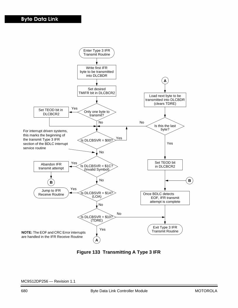
Byte Data Link
MC9S12DP256 — Revision 1.1
680 Byte Data Link Controller Module MOTOROLA
Figure 133 Transmitting A Type 3 IFR
Enter Type 3 IFRTransmit Routine
Set desiredTMIFR bit in DLCBCR2
Is DLCBSVR = $00?Yes
No
Load next byte to betransmitted into DLCBDR
(clears TDRE)
Is DLCBSVR = $1C?Yes
No
Is DLCBSVR = $14?Yes
No
Is DLCBSVR = $10?
Yes
No
(TDRE)
(LOA)
(Invalid Symbol)
Is this the last
Yes
No
byte?
B
Jump to IFRReceive Routine Once BDLC detects
EOF, IFR transmit
Set TEOD bitin DLCBCR2
attempt is complete
Exit Type 3 IFRTransmit Routine
Abandon IFRtransmit attempt
For interrupt driven systems, this marks the beginning of the transmit Type 3 IFR section of the BDLC interrupt service routine
NOTE: The EOF and CRC Error interrupts are handled in the IFR Receive Routine
Write first IFRbyte to be transmitted
into DLCBDR
Set TEOD bit in Only one byte toYes
No
transmit?DLCBCR2
A
B
A

Byte Data Link Controller ModuleReceiving An In-Frame Response (IFR)
MC9S12DP256 — Revision 1.1
MOTOROLA Byte Data Link Controller Module 681
Receiving An In-Frame Response (IFR)
Receiving an In-Frame Response with the BDLC is very similar to receiving a message frame. As each byte of an IFR is received, the DLCBSVR will indicate this to the CPU. An EOF indication in the DLCBSVR indicates that the IFR (and message) is complete. Also, the IMSG bit can also be used to command the BDLC to mask any further network activity from the CPU, including IFR bytes being received, until the next valid SOF is received.
NOTE: As with a message transmission, the IMSG bit should never be used to ignore the BDLC’s own IFR transmissions. This is again due to the DLCBSVR bits being inhibited from updating until IMSG is cleared, preventing the CPU from detecting any IFR-related state changes which may be of interest.
Receiving an IFR with the BDLC
Receiving an IFR from the SAE J1850 bus requires the same procedure that receiving a message does, except that as each byte is received the Received IFR Byte (RxIFR) state is indicated in the DLCBSVR. All other actions are the same. For an illustration of the steps described below, refer to Receiving An IFR With the BDLC.
Step 1: When RxIFR Interrupt Occurs, Retrieve IFR Byte
When the first byte of an IFR following a valid EOD symbol is received that byte is placed in the DLCBDR, and an RxIFR state is reflected in the DLCBSVR. No indication of the EOD reception in made, since the RxIFR state will indicate that the main portion of the message has ended and the IFR portion has begun.
The RxIFR interrupt is cleared when the received IFR byte is read from the DLCBDR. Once this is done, no further CPU intervention is necessary until the next IFR byte is received, and this step is repeated. As with a message reception, all bytes of the IFR, including the CRC byte, will be placed into the DLCBDR as they are received for the CPU to retrieve.
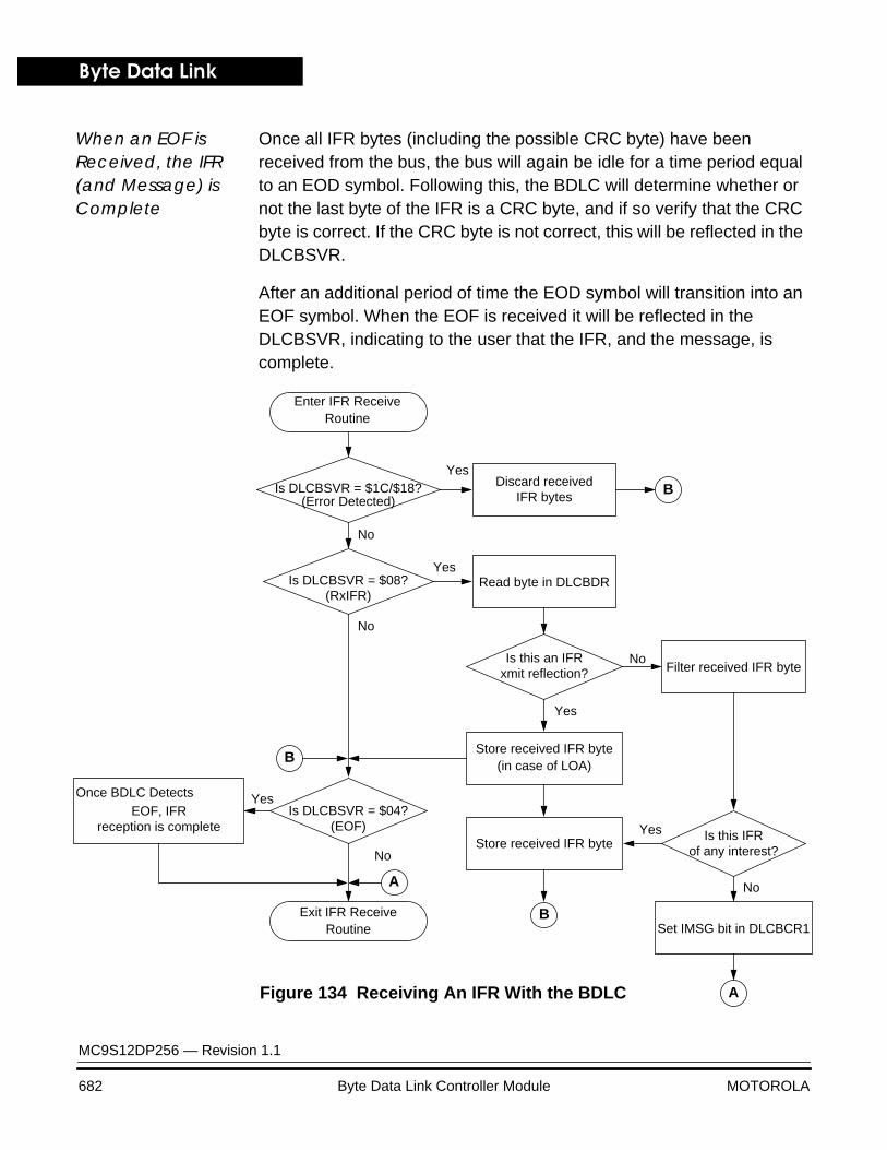
Byte Data Link
MC9S12DP256 — Revision 1.1
682 Byte Data Link Controller Module MOTOROLA
When an EOF is Received, the IFR (and Message) is Complete
Once all IFR bytes (including the possible CRC byte) have been received from the bus, the bus will again be idle for a time period equal to an EOD symbol. Following this, the BDLC will determine whether or not the last byte of the IFR is a CRC byte, and if so verify that the CRC byte is correct. If the CRC byte is not correct, this will be reflected in the DLCBSVR.
After an additional period of time the EOD symbol will transition into an EOF symbol. When the EOF is received it will be reflected in the DLCBSVR, indicating to the user that the IFR, and the message, is complete..
Figure 134 Receiving An IFR With the BDLC
Enter IFR ReceiveRoutine
Is DLCBSVR = $1C/$18?
No
Store received IFR byte(in case of LOA)
Is this IFRYes
No
Is DLCBSVR = $04?
No
Yes
(EOF)
of any interest?
Is this an IFR
Yes
Noxmit reflection?
Yes
Once BDLC DetectsEOF, IFR
Discard receivedIFR bytes
reception is complete
Yes
No
Is DLCBSVR = $08?
Exit IFR ReceiveRoutine
(Error Detected)
(RxIFR)Read byte in DLCBDR
Filter received IFR byte
Set IMSG bit in DLCBCR1
Store received IFR byte
B
B
B
A
A
Byte Data Link Controller ModuleSpecial BDLC Operations
MC9S12DP256 — Revision 1.1
MOTOROLA Byte Data Link Controller Module 683
Receiving IFR Exceptions
This basic IFR receiving flow can be interrupted for the same reasons as a normal message reception. The IFR receiving process can be adversely affected due to a CRC error, an Invalid or Out of Range Symbol or due to a receiver overrun caused by the CPU failing to service an RxIFR interrupt in a timely fashion. For a description of how these exceptions can affect the IFR receiving process, refer to Receiving Exceptions.
Special BDLC Operations
There are a few special operations which the BDLC can perform. What follows is a brief description of each of these functions and when they might be used.
Transmitting Or Receiving A Block Mode Message
The BDLC, because it handles each message on a byte-by-byte basis, has the inherent capability of handling messages any number of bytes in length. While during normal operation this requires the user to carefully monitor message lengths to ensure compliance with SAE J1850 message limits, often in a production or diagnostic environment messages which exceed the SAE J1850 limits can be beneficial. This is especially true when large amounts of configuration data need to be downloaded over the SAE J1850 network.
Because of the BDLC’s architecture, it can both transmit and receive messages of unlimited length. The CRC calculations, both for transmitting and receiving, are not limited to eight bytes, but will instead be calculated and verified using all bytes in the message, regardless of the number. All control bits, including TEOD and IMSG, also work in an identical manner, regardless of the length of the message.
To transmit or receive these “Block Mode” messages, no extra BDLC control functions must be performed. The user simply transmits or receives as many bytes as desired in one message frame, and the BDLC will operate just as if a message of normal length was being used.
Byte Data Link
MC9S12DP256 — Revision 1.1
684 Byte Data Link Controller Module MOTOROLA
Receiving A Message In 4X Mode
In a diagnostic or production environment large amounts of data may need to be downloaded across the network to a component or module. This data is often sent in a large “Block Mode” message (see above) which violates the SAE J1850 limit for message length. In order to speed up the downloading of these large blocks of data, they are sometimes transmitted at four times (4X) the normal bit rate for the Variable Pulse Width modulation version of SAE J1850. This higher speed transmission, nominally 41.6kbps, allows these large blocks to be transmitted much more quickly.
The BDLC is designed to receive (but not transmit) messages transmitted at this higher speed. By setting the RX4XE bit in DLCBCR2, the user can command the BDLC to receive any message sent over the network at a 4X rate.
If the BDLC is placed in this 4X mode, messages transmitted at the normal bit rate will not be received correctly. Likewise, 4X messages transmitted on the SAE J1850 bus when the BDLC is in normal mode will be interpreted as noise on the network by the BDLC. The RX4XE bit is not affected by entry or exit from BDLC stop or wait modes. For more information on the RX4XE bit, refer to RX4XE — Receive 4X Enable (Bit 5).
Modes of Operation
The BDLC has 6 main modes of operation which interact with the power supplies, pins, and the rest of the MCU as shown below. The operation of the BDLC in Normal and Special Modes are described later in this section.
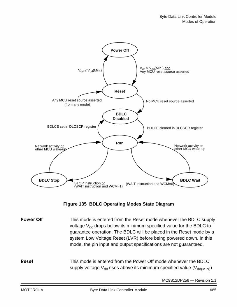
Byte Data Link Controller ModuleModes of Operation
MC9S12DP256 — Revision 1.1
MOTOROLA Byte Data Link Controller Module 685
Figure 135 BDLC Operating Modes State Diagram
Power Off This mode is entered from the Reset mode whenever the BDLC supply voltage Vdd drops below its minimum specified value for the BDLC to guarantee operation. The BDLC will be placed in the Reset mode by a system Low Voltage Reset (LVR) before being powered down. In this mode, the pin input and output specifications are not guaranteed.
Reset This mode is entered from the Power Off mode whenever the BDLC supply voltage Vdd rises above its minimum specified value (Vdd(MIN))
Vdd > Vdd(Min.) and
Power Off
Reset
BDLC Stop
Run
Vdd ≤ Vdd(Min.)
STOP instruction or
(from any mode)
BDLC Wait
Network activity or
(WAIT instruction and WCM=1)(WAIT instruction and WCM=0)
Any MCU reset source asserted No MCU reset source asserted
Any MCU reset source asserted
Network activity orother MCU wake-up other MCU wake-up
BDLCE cleared in DLCSCR register
BDLC
BDLCE set in DLCSCR register
Disabled
Byte Data Link
MC9S12DP256 — Revision 1.1
686 Byte Data Link Controller Module MOTOROLA
and some MCU reset source is asserted. To prevent the BDLC from entering an unknown state, the internal MCU reset is asserted while powering up the BDLC. BDLC Reset mode is also entered from any other mode as soon as one of the MCU’s possible reset sources (e.g. LVR, POR, COP watchdog, Reset pin etc.) is asserted.
In this mode, the internal BDLC voltage references are operative, Vdd is supplied to the internal circuits, which are held in their reset state and the internal BDLC system clock is running. Registers will assume their reset condition. Outputs are held in their programmed Reset state, inputs and network activity are ignored.
BDLC Disabled This mode is entered from the Reset mode after all MCU reset sources are no longer asserted. It is entered from the Run mode whenever the BDLCE bit in the DLCSCR register is cleared.
In this mode the mux interface clock (fbdlc) is stopped to conserve power and allow the BDLC to be configured for proper operation on the J1850 bus. The IP bus interface clocks are left running in this mode to allow access to all BDLC registers for initialization.
Run This mode is entered from the BDLC Disabled mode when the BDLCE bit in the DLCSCR register is set. It is entered from the BDLC Wait mode whenever activity is sensed on the J1850 bus or some other MCU source wakes the CPU out of Wait mode.
It is entered from the BDLC Stop mode whenever network activity is sensed or some other MCU source wakes the CPU out of Stop mode. Messages will not be received properly until the clocks have stabilized and the CPU is also in the Run mode.
In this mode, normal network operation takes place. The user should ensure that all BDLC transmissions have ceased, by reading the IDLE bit in the DLCBSTAT register, before exiting this mode.
BDLC Wait This power conserving mode is automatically entered from the Run mode whenever the CPU executes a WAIT instruction and if the WCM
Byte Data Link Controller ModuleModes of Operation
MC9S12DP256 — Revision 1.1
MOTOROLA Byte Data Link Controller Module 687
bit in the DLCBCR1 register is previously cleared. In this mode, the BDLC internal clocks continue to run. Any activity on the J1850 network will cause the BDLC to exit BDLC Wait mode and generate an unmaskable interrupt of the CPU. This Wakeup interrupt state is reflected in the DLCBSVR, encoded as the highest priority interrupt. This interrupt can be cleared by the CPU with a read of the DLCBSVR.
Wakeup from BDLC Wait with CPU in WAIT
If the CPU executes the WAIT instruction and the BDLC enters the WAIT mode (WCM = 0), the clocks to the BDLC as well as the clocks in the MCU continue to run. Therefore, the message which wakes up the BDLC from WAIT and the CPU from WAIT mode will also be received correctly by the BDLC. This is because all of the required clocks continue to run in the BDLC in WAIT mode.The wakeup behavior of the BDLC applies regardless of whether the BDLC is in normal or 4X mode when the WAIT instruction is executed.
BDLC Stop This power conserving mode is automatically entered from the Run mode whenever the CPU executes a STOP instruction, or if the CPU executes a WAIT instruction and the WCM bit in the DLCBCR1 register is previously set. In this mode, the BDLC internal clocks are stopped. Any activity on the network will cause the BDLC to exit BDLC Stop mode and generate an unmaskable interrupt of the CPU. This Wakeup interrupt state is reflected in the DLCBSVR, encoded as the highest priority interrupt. This interrupt can be cleared by the CPU with a read of the DLCBSVR. Depending upon which low-power mode instruction the CPU executes to cause the BDLC to enter BDLC Stop, the message which wakes up the BDLC (and the CPU) may or may not be received. There are two different possibilities, both of which is described below. These descriptions apply regardless of whether the BDLC is in normal or 4X mode when the STOP or WAIT instruction is executed.
Wakeup from BDLC Stop with CPU in STOP
When the CPU executes the STOP instruction, all clocks in the MCU, including clocks to the BDLC, are turned off. Therefore, the message which wakes up the BDLC and the CPU from STOP mode will not be received. This is due primarily to the amount of time required for the MCU’s oscillator to stabilize before the clocks can be applied internally to the other MCU modules, including the BDLC.

Byte Data Link
MC9S12DP256 — Revision 1.1
688 Byte Data Link Controller Module MOTOROLA
Wakeup from BDLC Stop with CPU in WAIT
If the CPU executes the WAIT instruction and the BDLC enters the Stop mode (WCM = 1), the clocks to the BDLC are turned off, but the clocks in the MCU continue to run. Therefore, the message which wakes up the BDLC from Stop and the CPU from WAIT mode will be received correctly by the BDLC. The is because very little time is required for the CPU to turn the clocks to the BDLC back on once the Wakeup interrupt occurs.
NOTE: While the BDLC will correctly receive a message which arrives when the BDLC is in Stop mode or Wait mode and the MCU is in WAIT mode, if the user enters this mode while a message is being received, the data in the message will become corrupted. This is due to the steps required for the BDLC to resume operation upon exiting Stop mode or Wait mode, and its subsequent resynchronization with the SAE J1850 bus.
Digital Loopback When a bus fault has been detected, the digital loopback mode is used to determine if the fault condition is caused by failure in the node’s internal circuits or elsewhere in the network, including the node’s analog physical interface. In this mode, the input to the digital filter is disconnected from the receive pin input (RxP). The input to the digital filter is then connected to the transmitter output to form the loopback connection. The transmit pin (TxP) is negated and will always drive a passive state onto the bus. Digital loopback mode is entered by setting the DLOOP bit in BDLC Control Register 2 (DLCBCR2).
Normal and Emulation Mode Operation
The BDLC operates in the same manner in all Normal and Emulation Modes. All BDLC registers can be read and written except those that are reserved, unimplemented, or write once. The user must be careful not to unintentionally write a register when using 16-bit writes in order to avoid unexpected BDLC behavior.
Special Mode Operation
Some aspects of BDLC operation can be modified in special test mode. This mode is reserved for internal use only.
Byte Data Link Controller ModuleInterrupt Operation
MC9S12DP256 — Revision 1.1
MOTOROLA Byte Data Link Controller Module 689
Interrupt Operation
The BDLC will generate an Interrupt Request to the CPU when a BDLC interrupt source is pending in the DLCBSVR. All DLCBSVR interrupts except the Wakeup Interrupt (DLCBSVR=$20) can be masked by clearing the IE bit in DLCBCR1. Refer to BDLC State Vector Register (DLCBSVR) for a description of the BDLC interrupt sources and how to service them.
Low Power Options
The BDLC can save power in Disabled, Wait, and Stop modes. A complete description of what the BDLC does while in a low power mode can be found in Modes of Operation.

Byte Data Link
MC9S12DP256 — Revision 1.1
690 Byte Data Link Controller Module MOTOROLA

MC9S12DP256 — Revision 1.1
MOTOROLA Background Debug Module (BDM) 691
Background Debug Module (BDM)Background Debug Module (BDM)
Contents
Overview . . . . . . . . . . . . . . . . . . . . . . . . . . . . . . . . . . . . . . . . . . . . . . 691Interface Signals . . . . . . . . . . . . . . . . . . . . . . . . . . . . . . . . . . . . . . . . 692Registers . . . . . . . . . . . . . . . . . . . . . . . . . . . . . . . . . . . . . . . . . . . . . . 693Operation . . . . . . . . . . . . . . . . . . . . . . . . . . . . . . . . . . . . . . . . . . . . . 698Modes of Operation. . . . . . . . . . . . . . . . . . . . . . . . . . . . . . . . . . . . . . 710Low-Power Options. . . . . . . . . . . . . . . . . . . . . . . . . . . . . . . . . . . . . . 711Interrupt Operation . . . . . . . . . . . . . . . . . . . . . . . . . . . . . . . . . . . . . . 711
Overview
The Background Debug Mode (BDM) sub-block is a single-wire, background debug system implemented in on-chip hardware for minimal CPU intervention. All interfacing with the BDM is done via the BKGD pin.
Features • Single-wire communication with host development system
• Active out of reset in special single-chip mode
• Nine hardware commands using free cycles, if available, for minimal CPU intervention
• Hardware commands not requiring active BDM
• 15 firmware commands execute from the standard BDM firmware lookup table
• Instruction tagging capability
• Software control of BDM operation during wait mode
• Software selectable clocks
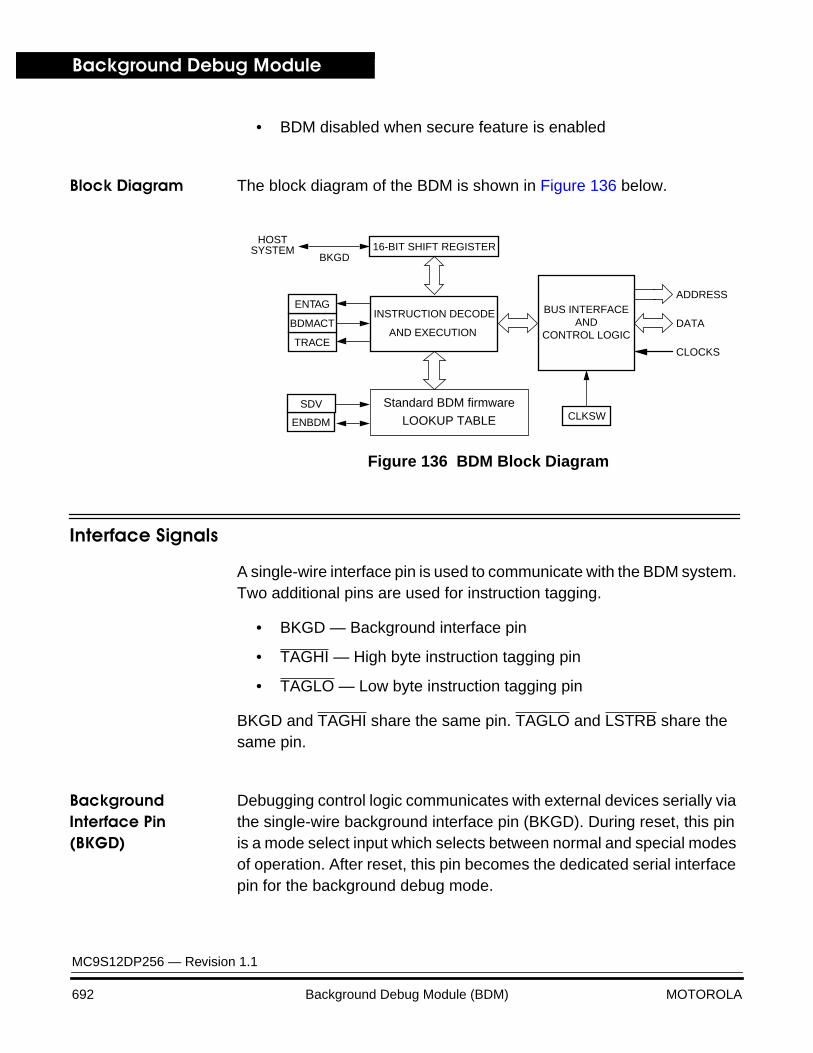
Background Debug Module
MC9S12DP256 — Revision 1.1
692 Background Debug Module (BDM) MOTOROLA
• BDM disabled when secure feature is enabled
Block Diagram The block diagram of the BDM is shown in Figure 136 below.
Figure 136 BDM Block Diagram
Interface Signals
A single-wire interface pin is used to communicate with the BDM system. Two additional pins are used for instruction tagging.
• BKGD — Background interface pin
• TAGHI — High byte instruction tagging pin
• TAGLO — Low byte instruction tagging pin
BKGD and TAGHI share the same pin. TAGLO and LSTRB share the same pin.
Background Interface Pin (BKGD)
Debugging control logic communicates with external devices serially via the single-wire background interface pin (BKGD). During reset, this pin is a mode select input which selects between normal and special modes of operation. After reset, this pin becomes the dedicated serial interface pin for the background debug mode.
ENBDMCLKSW
BDMACT
ENTAG
TRACE
SDV
16-BIT SHIFT REGISTERBKGD
CLOCKS
DATA
ADDRESS
HOSTSYSTEM
BUS INTERFACEAND
CONTROL LOGICAND EXECUTION
INSTRUCTION DECODE
LOOKUP TABLE
Standard BDM firmware
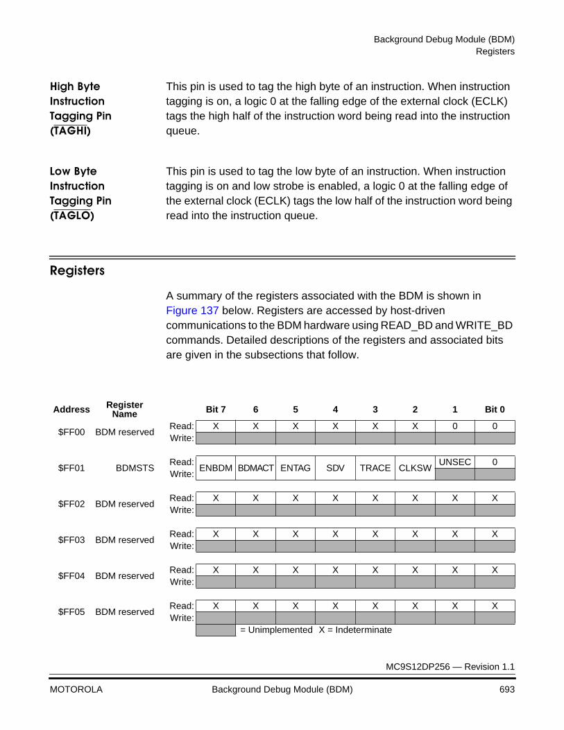
Background Debug Module (BDM)Registers
MC9S12DP256 — Revision 1.1
MOTOROLA Background Debug Module (BDM) 693
High Byte Instruction Tagging Pin (TAGHI)
This pin is used to tag the high byte of an instruction. When instruction tagging is on, a logic 0 at the falling edge of the external clock (ECLK) tags the high half of the instruction word being read into the instruction queue.
Low Byte Instruction Tagging Pin (TAGLO)
This pin is used to tag the low byte of an instruction. When instruction tagging is on and low strobe is enabled, a logic 0 at the falling edge of the external clock (ECLK) tags the low half of the instruction word being read into the instruction queue.
Registers
A summary of the registers associated with the BDM is shown in Figure 137 below. Registers are accessed by host-driven communications to the BDM hardware using READ_BD and WRITE_BD commands. Detailed descriptions of the registers and associated bits are given in the subsections that follow.
Address Register Name Bit 7 6 5 4 3 2 1 Bit 0
$FF00 BDM reservedRead: X X X X X X 0 0Write:
$FF01 BDMSTSRead:
ENBDM BDMACT ENTAG SDV TRACE CLKSWUNSEC 0
Write:
$FF02 BDM reservedRead: X X X X X X X XWrite:
$FF03 BDM reservedRead: X X X X X X X XWrite:
$FF04 BDM reservedRead: X X X X X X X XWrite:
$FF05 BDM reservedRead: X X X X X X X XWrite:
= Unimplemented X = Indeterminate
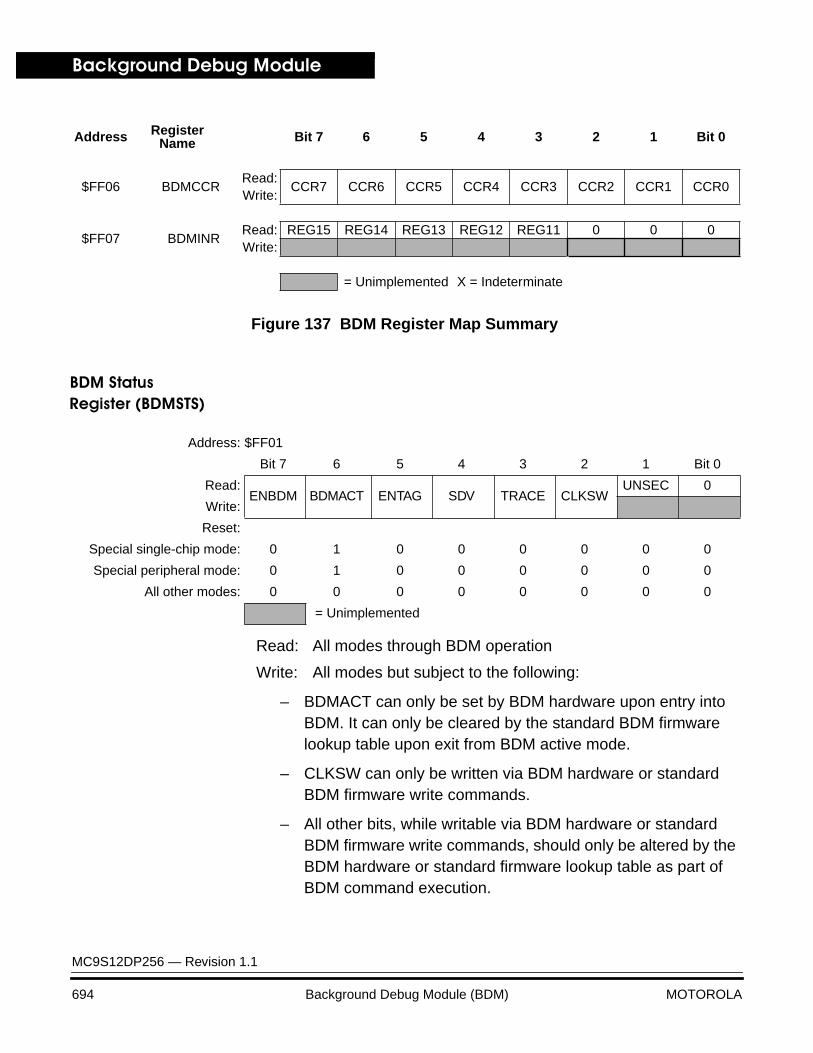
Background Debug Module
MC9S12DP256 — Revision 1.1
694 Background Debug Module (BDM) MOTOROLA
Figure 137 BDM Register Map Summary
BDM Status Register (BDMSTS)
Read: All modes through BDM operation
Write: All modes but subject to the following:
– BDMACT can only be set by BDM hardware upon entry into BDM. It can only be cleared by the standard BDM firmware lookup table upon exit from BDM active mode.
– CLKSW can only be written via BDM hardware or standard BDM firmware write commands.
– All other bits, while writable via BDM hardware or standard BDM firmware write commands, should only be altered by the BDM hardware or standard firmware lookup table as part of BDM command execution.
$FF06 BDMCCRRead:
CCR7 CCR6 CCR5 CCR4 CCR3 CCR2 CCR1 CCR0Write:
$FF07 BDMINRRead: REG15 REG14 REG13 REG12 REG11 0 0 0Write:
Address Register Name Bit 7 6 5 4 3 2 1 Bit 0
= Unimplemented X = Indeterminate
Address: $FF01
Bit 7 6 5 4 3 2 1 Bit 0
Read:ENBDM BDMACT ENTAG SDV TRACE CLKSW
UNSEC 0
Write:
Reset:
Special single-chip mode: 0 1 0 0 0 0 0 0
Special peripheral mode: 0 1 0 0 0 0 0 0
All other modes: 0 0 0 0 0 0 0 0
= Unimplemented
Background Debug Module (BDM)Registers
MC9S12DP256 — Revision 1.1
MOTOROLA Background Debug Module (BDM) 695
– ENBDM should only be set via a BDM hardware command if the BDM firmware commands are needed. (This does not apply in Special Single Chip Mode).
ENBDM — Enable BDM
This bit controls whether the BDM is enabled or disabled. When enabled, BDM can be made active to allow firmware commands to be executed. When disabled, BDM cannot be made active but BDM hardware commands are still allowed.
1 = BDM enabled0 = BDM disabled
NOTE: ENBDM is set by the firmware immediately out of reset in special single-chip mode.
BDMACT — BDM active status
This bit becomes set upon entering BDM. The standard BDM firmware lookup table is then enabled and put into the memory map. BDMACT is cleared by a carefully timed store instruction in the standard BDM firmware as part of the exit sequence to return to user code and remove the BDM memory from the map.
1 = BDM active0 = BDM not active
ENTAG — Tagging enable
This bit indicates whether instruction tagging in enabled or disabled. It is set when the TAGGO command is executed and cleared when BDM is entered. The serial system is disabled and the tag function enabled 16 cycles after this bit is written. BDM cannot process serial commands while tagging is active.
1 = Tagging enabled0 = Tagging not enabled, or BDM active
SDV — Shift data valid
This bit is set and cleared by the BDM hardware. It is set after data has been transmitted as part of a firmware read command or after data has been received as part of a firmware write command. It is
Background Debug Module
MC9S12DP256 — Revision 1.1
696 Background Debug Module (BDM) MOTOROLA
cleared when the next BDM command has been received or BDM is exited. SDV is used by the standard BDM firmware to control program flow execution.
1 = Data phase of command is complete0 = Data phase of command not complete
TRACE — TRACE1 BDM firmware command is being executed
This bit gets set when a BDM TRACE1 firmware command is first recognized. It will stay set as long as continuous back-to-back TRACE1 commands are executed. This bit will get cleared when the next command that is not a TRACE1 command is recognized.
1 = TRACE1 command is being executed0 = TRACE1 command is not being executed
CLKSW — Clock switch
The CLKSW bit controls which clock the BDM operates with. It is only writable from a hardware BDM command. A 150 cycle delay at the clock speed that is active during the data portion of the command will occur before the new clock source is guaranteed to be active. The start of the next BDM command uses the new clock for timing subsequent BDM communications.
1 = BDM system operates with bus rate0 = BDM system operates with alternate clock
WARNING: Care must be taken when CLKSW=0 to ensure that the alternate clock frequency does not exceed that of the bus clock frequency. The BDM will not operate correctly if this condition exists.
UNSEC — Unsecure
This bit is only writable in special single chip mode from a hardware BDM command and always gets reset to zero. It is in a zero state as secure mode is entered so that the secure BDM firmware lookup table is enabled and put into the memory map along with the standard BDM firmware lookup table.
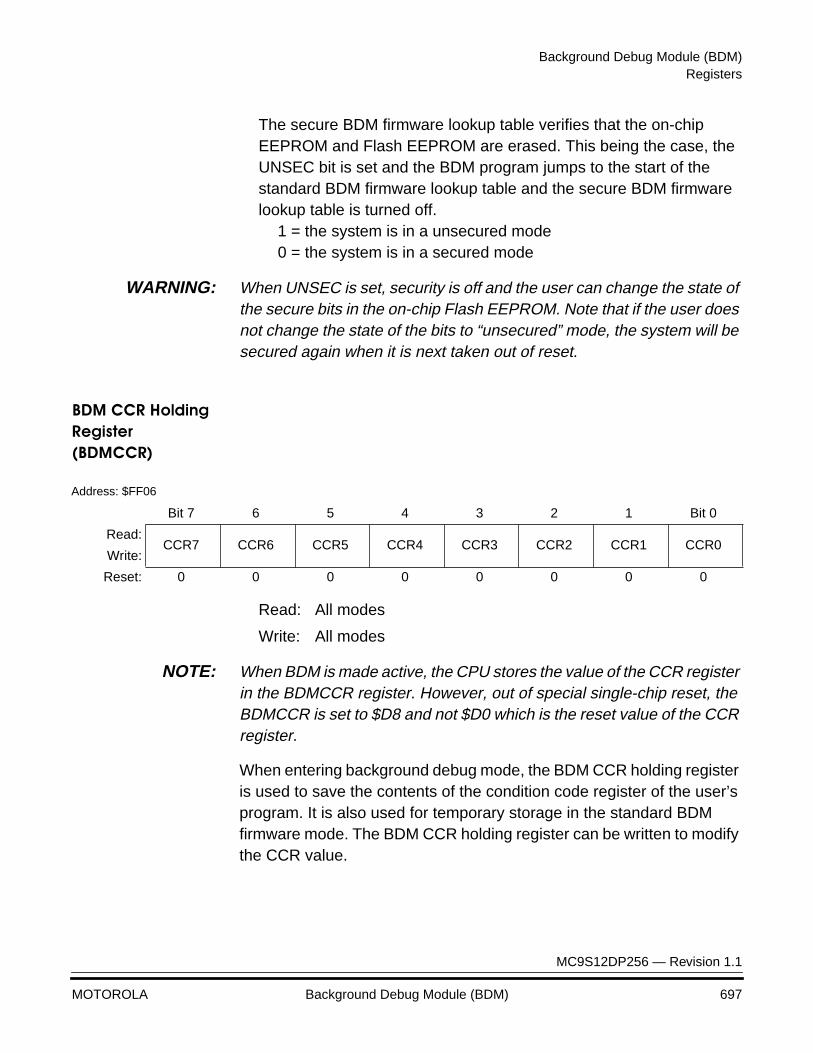
Background Debug Module (BDM)Registers
MC9S12DP256 — Revision 1.1
MOTOROLA Background Debug Module (BDM) 697
The secure BDM firmware lookup table verifies that the on-chip EEPROM and Flash EEPROM are erased. This being the case, the UNSEC bit is set and the BDM program jumps to the start of the standard BDM firmware lookup table and the secure BDM firmware lookup table is turned off.
1 = the system is in a unsecured mode0 = the system is in a secured mode
WARNING: When UNSEC is set, security is off and the user can change the state of the secure bits in the on-chip Flash EEPROM. Note that if the user does not change the state of the bits to “unsecured” mode, the system will be secured again when it is next taken out of reset.
BDM CCR Holding Register (BDMCCR)
Read: All modes
Write: All modes
NOTE: When BDM is made active, the CPU stores the value of the CCR register in the BDMCCR register. However, out of special single-chip reset, the BDMCCR is set to $D8 and not $D0 which is the reset value of the CCR register.
When entering background debug mode, the BDM CCR holding register is used to save the contents of the condition code register of the user’s program. It is also used for temporary storage in the standard BDM firmware mode. The BDM CCR holding register can be written to modify the CCR value.
Address: $FF06
Bit 7 6 5 4 3 2 1 Bit 0
Read:CCR7 CCR6 CCR5 CCR4 CCR3 CCR2 CCR1 CCR0
Write:
Reset: 0 0 0 0 0 0 0 0

Background Debug Module
MC9S12DP256 — Revision 1.1
698 Background Debug Module (BDM) MOTOROLA
BDM Internal Register Position Register (BDMINR)
(
Read: All modes
Write: Never
REG15–REG11 — Internal register map position
These five bits show the state of the upper five bits of the base address for the system’s relocatable register block. BDMINR is a shadow of the INITRG register which maps the register block to any 2K byte space within the first 32K bytes of the 64K byte address space.
Operation
The BDM receives and executes commands from a host via a single wire serial interface. There are two types of BDM commands, namely, hardware commands and firmware commands.
Hardware commands are used to read and write target system memory locations and to enter active background debug mode (see BDM Hardware Commands). Target system memory includes all memory that is accessible by the CPU.
Firmware commands are used to read and write CPU resources and to exit from active background debug mode (see Standard BDM Firmware Commands). The CPU resources referred to are the accumulator (D), X index register (X), Y index register (Y), stack pointer (SP), and program counter (PC).
Address: $FF07
Bit 7 6 5 4 3 2 1 Bit 0
Read: REG15 REG14 REG13 REG12 REG11 0 0 0
Write:
Reset: 0 0 0 0 0 0 0 0
= Unimplemented
Background Debug Module (BDM)Operation
MC9S12DP256 — Revision 1.1
MOTOROLA Background Debug Module (BDM) 699
Hardware commands can be executed at any time and in any mode excluding a few exceptions as highlighted in Modes of Operation below. Firmware commands can only be executed when the system is in active background debug mode (BDM).
Security If the user resets into special single chip mode with the system secured, a SECURE BDM FIRMWARE lookup table is brought into the map overlapping a portion of the STANDARD BDM FIRMWARE lookup table. The secure BDM firmware verifies that the on-chip EEPROM and Flash EEPROM are erased. This being the case, the UNSEC bit will get set. The BDM program jumps to the start of the standard BDM firmware and the secure BDM firmware is turned off.
Enabling and Activating BDM
The system must be in active BDM to execute standard BDM firmware commands. BDM can be activated only after being enabled. BDM is enabled by setting the ENBDM bit in the BDM status (BDMSTS) register. The ENBDM bit is set by writing to the BDM status (BDMSTS) register, via the single-wire interface, using a hardware command such as WRITE_BD_BYTE.
After being enabled, BDM is activated by one of the following1:
• Hardware BACKGROUND command
• BDM external instruction tagging mechanism
• CPU BGND instruction
• Breakpoint sub-block’s force or tag mechanism2
When BDM is activated, the CPU finishes executing the current instruction and then begins executing the firmware in the standard BDM firmware lookup table. When BDM is activated by the breakpoint sub-block, the type of breakpoint used determines if BDM becomes active before or after execution of the next instruction.
1. BDM is enabled and active immediately out of special single-chip reset (see Special Opera-tion).
2. This method is only available on systems that have a a Breakpoint sub-block.
Background Debug Module
MC9S12DP256 — Revision 1.1
700 Background Debug Module (BDM) MOTOROLA
NOTE: If an attempt is made to activate BDM before being enabled, the CPU resumes normal instruction execution after a brief delay. If BDM is not enabled, any hardware BACKGROUND commands issued are ignored by the BDM and the CPU is not delayed.
In active BDM, the BDM registers and standard BDM firmware lookup table are mapped to addresses $FF00 to $FFFF. BDM registers are mapped to addresses $FF00 to $FF07. The BDM uses these registers which are readable anytime by the BDM. These registers are not, however, readable by user programs.
BDM Hardware Commands
Hardware commands are used to read and write target system memory locations and to enter active background debug mode. Target system memory includes all memory that is accessible by the CPU such as on-chip RAM, EEPROM, Flash EEPROM, I/O and control registers, and all external memory.
Hardware commands are executed with minimal or no CPU intervention and do not require the system to be in active BDM for execution, although, they can still be executed in this mode. When executing a hardware command, the BDM sub-block waits for a free CPU bus cycle so that the background access does not disturb the running application program. If a free cycle is not found within 128 clock cycles, the CPU is momentarily frozen so that the BDM can steal a cycle. When the BDM finds a free cycle, the operation does not intrude on normal CPU operation provided that it can be completed in a single cycle. However, if an operation requires multiple cycles, the CPU is frozen until the operation is complete, even though the BDM found a free cycle.

Background Debug Module (BDM)Operation
MC9S12DP256 — Revision 1.1
MOTOROLA Background Debug Module (BDM) 701
The BDM hardware commands are listed in Table 121.
The READ_BD and WRITE_BD commands allow access to the BDM register locations. These locations are not normally in the system memory map but share addresses with the application in memory. To distinguish between physical memory locations that share the same address, BDM memory resources are enabled just for the READ_BD and WRITE_BD access cycle. This allows the BDM to access BDM locations unobtrusively, even if the addresses conflict with the application memory map.
Standard BDM Firmware Commands
Firmware commands are used to access and manipulate CPU resources. The system must be in active BDM to execute standard BDM firmware commands (see Enabling and Activating BDM). Normal
Table 121 Hardware Commands
Command Opcode (hex) Data Description
BACKGROUND 90 None Enter background mode if firmware is enabled.
READ_BD_BYTE E416-bit address16-bit data out
Read from memory with standard BDM firmware lookup table in map. Odd address data on low byte; even address data on high byte
READ_BD_WORD EC16-bit address16-bit data out
Read from memory with standard BDM firmware lookup table in map. Must be aligned access.
READ_BYTE E016-bit address16-bit data out
Read from memory with standard BDM firmware lookup table out of map. Odd address data on low byte; even address data on high byte
READ_WORD E816-bit address16-bit data out
Read from memory with standard BDM firmware lookup table out of map. Must be aligned access.
WRITE_BD_BYTE C416-bit address16-bit data in
Write to memory with standard BDM firmware lookup table in map. Odd address data on low byte; even address data on high byte
WRITE_BD_WORD CC16-bit address16-bit data in
Write to memory with standard BDM firmware lookup table in map. Must be aligned access
WRITE_BYTE C016-bit address16-bit data in
Write to memory with standard BDM firmware lookup table out of map. Odd address data on low byte; even address data on high byte
WRITE_WORD C816-bit address16-bit data in
Write to memory with standard BDM firmware lookup table out of map. Must be aligned access.

Background Debug Module
MC9S12DP256 — Revision 1.1
702 Background Debug Module (BDM) MOTOROLA
instruction execution is suspended while the CPU executes the firmware located in the standard BDM firmware lookup table. The hardware command BACKGROUND is the usual way to activate BDM.
As the system enters active BDM, the standard BDM firmware lookup table and BDM registers become visible in the on-chip memory map at $FF00-$FFFF, and the CPU begins executing the standard BDM firmware. The standard BDM firmware watches for serial commands and executes them as they are received. The firmware commands are shown in Table 122.
Table 122 Firmware Commands
Command Opcode (hex) Data Description
READ_NEXT 62 16-bit data out Increment X by 2 (X = X + 2), then read word X points to.
READ_PC 63 16-bit data out Read program counter.
READ_D 64 16-bit data out Read D accumulator.
READ_X 65 16-bit data out Read X index register.
READ_Y 66 16-bit data out Read Y index register.
READ_SP 67 16-bit data out Read stack pointer.
WRITE_NEXT 42 16-bit data inIncrement X by 2 (X=X+2), then write word to location pointed to by X.
WRITE_PC 43 16-bit data in Write program counter.
WRITE_D 44 16-bit data in Write D accumulator.
WRITE_X 45 16-bit data in Write X index register.
WRITE_Y 46 16-bit data in Write Y index register.
WRITE_SP 47 16-bit data in Write stack pointer.
GO 08 none Go to user program.
TRACE1 10 none Execute one user instruction then return to active BDM.
TAGGO 18 none Enable tagging and go to user program.
Background Debug Module (BDM)Operation
MC9S12DP256 — Revision 1.1
MOTOROLA Background Debug Module (BDM) 703
BDM Command Structure
Hardware and firmware BDM commands start with an 8-bit opcode followed by a 16-bit address and/or a 16-bit data word depending on the command. All the read commands return 16 bits of data despite the byte or word implication in the command name.
NOTE: 8-bit reads return 16-bits of data, of which, only one byte will contain valid data. If reading an even address, the valid data will appear in the MSB. If reading an odd address, the valid data will appear in the LSB.
NOTE: 16-bit misaligned reads and writes are not allowed. If attempted, the BDM will ignore the least significant bit of the address and will assume an even address from the remaining bits.
For hardware data read commands, the external host must wait 150 target clock cycles1 after sending the address before attempting to obtain the read data. This is to be certain that valid data is available in the BDM shift register, ready to be shifted out. For hardware write commands, the external host must wait 150 target clock cycles after sending the data to be written before attempting to send a new command. This is to avoid disturbing the BDM shift register before the write has been completed. The 150 target clock cycle delay in both cases includes the maximum 128 cycle delay that can be incurred as the BDM waits for a free cycle before stealing a cycle.
For firmware read commands, the external host must wait 32 target clock cycles after sending the command opcode before attempting to obtain the read data. This allows enough time for the requested data to be made available in the BDM shift register, ready to be shifted out. For firmware write commands, the external host must wait 32 target clock cycles after sending the data to be written before attempting to send a new command. This is to avoid disturbing the BDM shift register before the write has been completed.
The external host should wait 64 target clock cycles after a TRACE1 or GO command before starting any new serial command. This is to allow the CPU to exit gracefully from the standard BDM firmware lookup table
1. Target clock cycles are cycles measured using the target system’s serial clock rate. See BDM Serial Interface and BDM Status Register (BDMSTS) for information on how serial clock rate is selected.
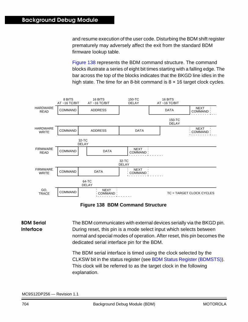
Background Debug Module
MC9S12DP256 — Revision 1.1
704 Background Debug Module (BDM) MOTOROLA
and resume execution of the user code. Disturbing the BDM shift register prematurely may adversely affect the exit from the standard BDM firmware lookup table.
Figure 138 represents the BDM command structure. The command blocks illustrate a series of eight bit times starting with a falling edge. The bar across the top of the blocks indicates that the BKGD line idles in the high state. The time for an 8-bit command is 8 × 16 target clock cycles.
Figure 138 BDM Command Structure
BDM Serial Interface
The BDM communicates with external devices serially via the BKGD pin. During reset, this pin is a mode select input which selects between normal and special modes of operation. After reset, this pin becomes the dedicated serial interface pin for the BDM.
The BDM serial interface is timed using the clock selected by the CLKSW bit in the status register (see BDM Status Register (BDMSTS)). This clock will be referred to as the target clock in the following explanation.
HARDWARE
HARDWARE
FIRMWARE
FIRMWARE
GO,
32-TC
TC = TARGET CLOCK CYCLES
COMMAND ADDRESS
150-TCDELAY
NEXT
DELAY
8 BITSAT ~16 TC/BIT
16 BITSAT ~16 TC/BIT
16 BITSAT ~16 TC/BIT
COMMAND ADDRESS DATANEXT
DATAREAD
WRITE
READ
WRITE
TRACE
COMMANDNEXT
COMMAND DATA
64-TCDELAY
NEXT
COMMAND
150-TCDELAY
32-TCDELAY
COMMAND
COMMAND
COMMAND
COMMANDDATA
NEXTCOMMAND
Background Debug Module (BDM)Operation
MC9S12DP256 — Revision 1.1
MOTOROLA Background Debug Module (BDM) 705
The BDM serial interface uses a clocking scheme in which the external host generates a falling edge on the BKGD pin to indicate the start of each bit time. This falling edge is sent for every bit whether data is transmitted or received. Data is transferred most significant bit (MSB) first at 16 target clock cycles per bit. The interface times out if 512 clock cycles occur between falling edges from the host.
The BKGD pin is a pseudo open-drain pin and has an weak on-chip active pull-up that is enabled at all times. It is assumed that there is an external pullup and that drivers connected to BKGD do not typically drive the high level. Since R-C rise time could be unacceptably long, the target system and host provide brief driven-high (speedup) pulses to drive BKGD to a logic 1. The source of this speedup pulse is the host for transmit cases and the target for receive cases.
The timing for host-to-target is shown in Figure 139 and that of target-to-host in Figure 140 and Figure 141 below. All four cases begin when the host drives the BKGD pin low to generate a falling edge. Since the host and target are operating from separate clocks, it can take the target system up to one full clock cycle to recognize this edge. The target measures delays from this perceived start of the bit time while the host measures delays from the point it actually drove BKGD low to start the bit up to one target clock cycle earlier. Synchronization between the host and target is established in this manner at the start of every bit time.
Figure 139 shows an external host transmitting a logic 1 and transmitting a logic 0 to the BKGD pin of a target system. The host is asynchronous to the target, so there is up to a one clock-cycle delay from the host-generated falling edge to where the target recognizes this edge as the beginning of the bit time. Ten target clock cycles later, the target senses the bit level on the BKGD pin. Internal glitch detect logic requires the pin be driven high no later that eight target clock cycles after the falling edge for a logic 1 transmission.
Since the host drives the high speedup pulses in these two cases, the rising edges look like digitally driven signals.
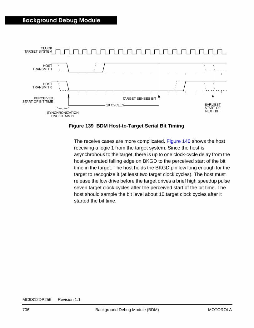
Background Debug Module
MC9S12DP256 — Revision 1.1
706 Background Debug Module (BDM) MOTOROLA
Figure 139 BDM Host-to-Target Serial Bit Timing
The receive cases are more complicated. Figure 140 shows the host receiving a logic 1 from the target system. Since the host is asynchronous to the target, there is up to one clock-cycle delay from the host-generated falling edge on BKGD to the perceived start of the bit time in the target. The host holds the BKGD pin low long enough for the target to recognize it (at least two target clock cycles). The host must release the low drive before the target drives a brief high speedup pulse seven target clock cycles after the perceived start of the bit time. The host should sample the bit level about 10 target clock cycles after it started the bit time.
EARLIESTSTART OFNEXT BIT
TARGET SENSES BIT
10 CYCLES
SYNCHRONIZATIONUNCERTAINTY
CLOCKTARGET SYSTEM
HOSTTRANSMIT 1
HOSTTRANSMIT 0
PERCEIVEDSTART OF BIT TIME

Background Debug Module (BDM)Operation
MC9S12DP256 — Revision 1.1
MOTOROLA Background Debug Module (BDM) 707
Figure 140 BDM Target-to-Host Serial Bit Timing (Logic 1)
Figure 141 shows the host receiving a logic 0 from the target. Since the host is asynchronous to the target, there is up to a one clock-cycle delay from the host-generated falling edge on BKGD to the start of the bit time as perceived by the target. The host initiates the bit time but the target finishes it. Since the target wants the host to receive a logic 0, it drives the BKGD pin low for 13 target clock cycles then briefly drives it high to speed up the rising edge. The host samples the bit level about 10 target clock cycles after starting the bit time.
HIGH-IMPEDANCE
EARLIESTSTART OFNEXT BIT
R-C RISE
10 CYCLES
10 CYCLES
HOST SAMPLESBKGD PIN
PERCEIVEDSTART OF BIT TIME
BKGD PIN
CLOCKTARGET SYSTEM
HOSTDRIVE TOBKGD PIN
TARGET SYSTEMSPEEDUP
PULSE
HIGH-IMPEDANCE
HIGH-IMPEDANCE

Background Debug Module
MC9S12DP256 — Revision 1.1
708 Background Debug Module (BDM) MOTOROLA
Figure 141 BDM Target-to-Host Serial Bit Timing (Logic 0)
Instruction Tracing When a TRACE1 command is issued to the BDM in active BDM, the CPU exits the standard BDM firmware and executes a single instruction in the user code. Once this has occurred, the CPU is forced to return to the standard BDM firmware and the BDM is active and ready to receive a new command. If the TRACE1 command is issued again, the next user instruction will be executed. This facilitates stepping or tracing through the user code one instruction at a time.
If an interrupt is pending when a TRACE1 command is issued, the interrupt stacking operation occurs but no user instruction is executed. Once back in standard BDM firmware execution, the program counter points to the first instruction in the interrupt service routine.
Instruction Tagging
The instruction queue and cycle-by-cycle CPU activity are reconstructible in real time or from trace history that is captured by a logic analyzer. However, the reconstructed queue cannot be used to stop the CPU at a specific instruction, because execution already has begun by the time an operation is visible outside the system. A separate instruction tagging mechanism is provided for this purpose.
EARLIESTSTART OFNEXT BIT
CLOCKTARGET SYS.
HOSTDRIVE TOBKGD PIN
BKGD PIN
PERCEIVEDSTART OF BIT TIME
10 CYCLES
10 CYCLES
HOST SAMPLESBKGD PIN
TARGET SYS.DRIVE AND
SPEEDUP PULSE
SPEEDUP PULSE
HIGH-IMPEDANCE
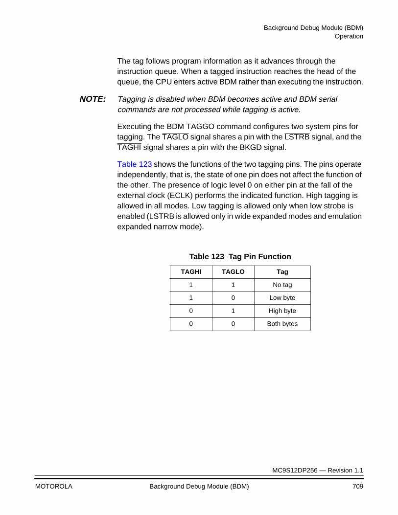
Background Debug Module (BDM)Operation
MC9S12DP256 — Revision 1.1
MOTOROLA Background Debug Module (BDM) 709
The tag follows program information as it advances through the instruction queue. When a tagged instruction reaches the head of the queue, the CPU enters active BDM rather than executing the instruction.
NOTE: Tagging is disabled when BDM becomes active and BDM serial commands are not processed while tagging is active.
Executing the BDM TAGGO command configures two system pins for tagging. The TAGLO signal shares a pin with the LSTRB signal, and the TAGHI signal shares a pin with the BKGD signal.
Table 123 shows the functions of the two tagging pins. The pins operate independently, that is, the state of one pin does not affect the function of the other. The presence of logic level 0 on either pin at the fall of the external clock (ECLK) performs the indicated function. High tagging is allowed in all modes. Low tagging is allowed only when low strobe is enabled (LSTRB is allowed only in wide expanded modes and emulation expanded narrow mode).
Table 123 Tag Pin Function
TAGHI TAGLO Tag
1 1 No tag
1 0 Low byte
0 1 High byte
0 0 Both bytes
Background Debug Module
MC9S12DP256 — Revision 1.1
710 Background Debug Module (BDM) MOTOROLA
Modes of Operation
BDM is available in all operating modes but must be enabled before firmware commands are executed.
Some system peripherals may have a control bit which allows suspending the peripheral function during background debug mode.
In special single-chip mode, background operation is enabled and active out of reset. This allows programming a system with blank memory.
BDM is also active out of special peripheral mode reset and can be turned off by clearing the BDMACT bit in the BDM status (BDMSTS) register. This allows testing of the BDM memory space as well as the user’s memory space.
NOTE: The BDM serial system should not be used in special peripheral mode since the CPU, which in other modes interfaces with the BDM to relinquish control of the bus during a free cycle or a steal operation, is not operating in this mode.
Normal Operation BDM operates the same in all normal modes.
Special Operation
Special single-chip mode
BDM is enabled and active immediately out of reset. This allows programming a system with blank memory.
Special peripheral mode
BDM is enabled and active immediately out of reset. BDM can be disabled by clearing the BDMACT bit in the BDM status (BDMSTS) register. The BDM serial system should not be used in special peripheral mode.
Emulation Modes In emulation modes, the BDM operates as in all normal modes.
Background Debug Module (BDM)Low-Power Options
MC9S12DP256 — Revision 1.1
MOTOROLA Background Debug Module (BDM) 711
Low-Power Options
Run Mode The BDM does not include disable controls that would conserve power during run mode.
Wait Mode The BDM cannot be used in wait mode if the system disables the clocks to the BDM.
Stop Mode The BDM is completely shutdown in stop mode.
Interrupt Operation
The BDM does not generate interrupt requests.

Background Debug Module
MC9S12DP256 — Revision 1.1
712 Background Debug Module (BDM) MOTOROLA

MC9S12DP256 — Revision 1.1
MOTOROLA Breakpoint (BKP) Module 713
Breakpoint (BKP) ModuleBreakpoint (BKP) Module
Contents
Overview . . . . . . . . . . . . . . . . . . . . . . . . . . . . . . . . . . . . . . . . . . . . . . 713Features . . . . . . . . . . . . . . . . . . . . . . . . . . . . . . . . . . . . . . . . . . . . . . 714Block Diagram. . . . . . . . . . . . . . . . . . . . . . . . . . . . . . . . . . . . . . . . . . 715External Pin Descriptions . . . . . . . . . . . . . . . . . . . . . . . . . . . . . . . . . 716Register Descriptions . . . . . . . . . . . . . . . . . . . . . . . . . . . . . . . . . . . . 716Functional Description. . . . . . . . . . . . . . . . . . . . . . . . . . . . . . . . . . . . 723Breakpoint Operating Modes . . . . . . . . . . . . . . . . . . . . . . . . . . . . . . 724Breakpoint Types . . . . . . . . . . . . . . . . . . . . . . . . . . . . . . . . . . . . . . . 725Modes of Operation. . . . . . . . . . . . . . . . . . . . . . . . . . . . . . . . . . . . . . 725Low Power Options . . . . . . . . . . . . . . . . . . . . . . . . . . . . . . . . . . . . . . 726Modes of Operation. . . . . . . . . . . . . . . . . . . . . . . . . . . . . . . . . . . . . . 725Interrupt Operation . . . . . . . . . . . . . . . . . . . . . . . . . . . . . . . . . . . . . . 726General Purpose I/O Ports . . . . . . . . . . . . . . . . . . . . . . . . . . . . . . . . 726
Overview
Hardware breakpoints are used to debug software on the STAR12 CPU by comparing actual address and data values to predetermined data in setup registers. A successful comparison will place the CPU in background debug mode (BDM) or initiate a software interrupt (SWI).
The Breakpoint Module contains two modes of operation:
1. Dual Address Mode, where a match on either of two addresses will cause a Software Interrupt (SWI) or cause the part to enter Background Debug Mode.
2. Full Breakpoint Mode, where a match on address and data will cause a Software Interrupt (SWI) or cause the part to enter Background Debug Mode.

Breakpoint (BKP) Module
MC9S12DP256 — Revision 1.1
714 Breakpoint (BKP) Module MOTOROLA
There are two types of breakpoints: tagged and forced. Forced breakpoints occur at the next instruction boundary if a match occurs and tagged breakpoints allow breaking just before a specific instruction executes. Tagged breakpoints will only occur on addresses. Tagging on data is not allowed; however, if this occurs, nothing will occur within the BKP module.
The breakpoint module allows breaking within a 256 byte address range and/or within expanded memory, allows matching of the data bus as well as address matching, allows breakpoints to match 8 bit or 16 bit data, and allows forced breakpoints to match on a read or write cycle.
Features
• Full or Dual Breakpoint Mode
– Compare on address and data (Full)
– Compare on either of two addresses (Dual)
• BDM or SWI Breakpoint
– Enter BDM on breakpoint (BDM)
– Execute SWI on breakpoint (SWI)
• Tagged or Forced Breakpoint
– Break just before a specific instruction will begin execution (TAG)
– Break on the first instruction boundary after a match occurs (Force)
• Single, Range, or Page address compares
– Compare on address (Single)
– Compare on address 256 byte (Range)
– Compare on any 16K Page (Page)
• Compare address on read or write on forced breakpoints
• High and/or low byte data compares
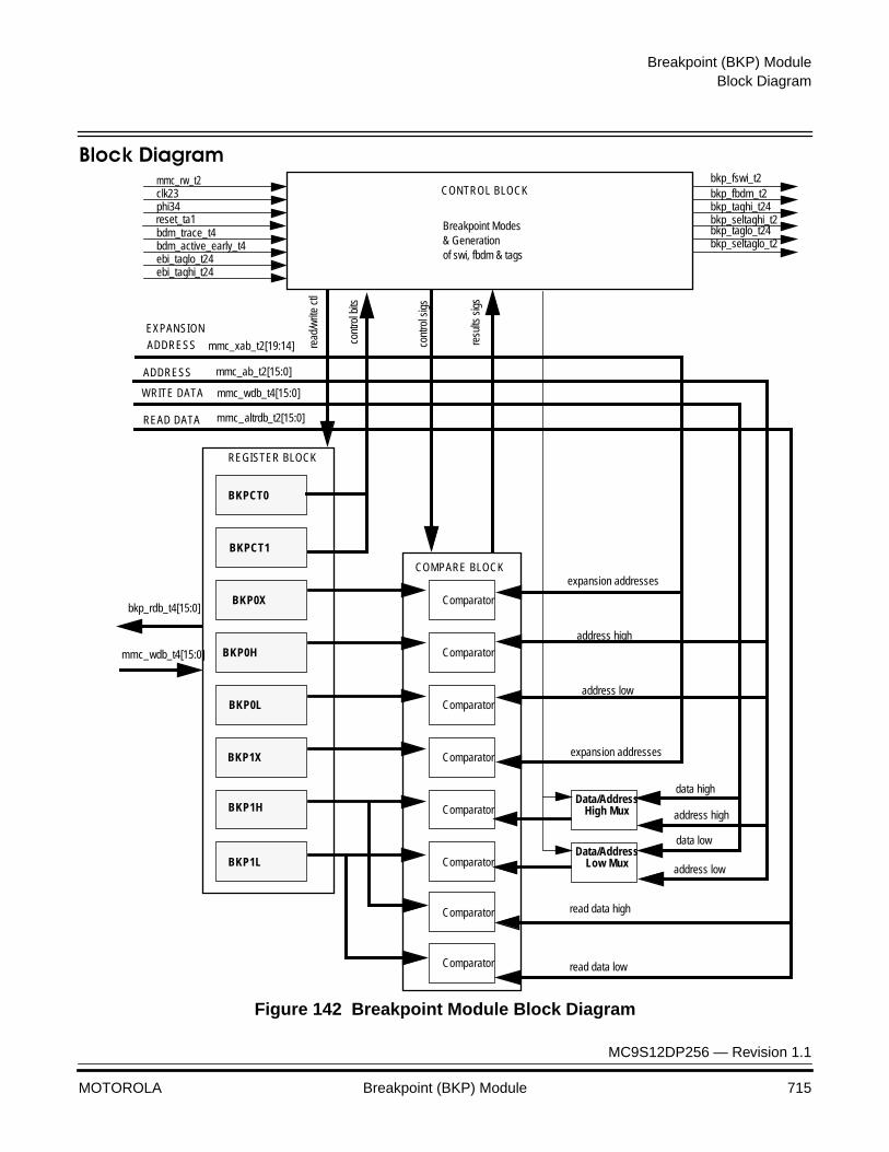
Breakpoint (BKP) ModuleBlock Diagram
MC9S12DP256 — Revision 1.1
MOTOROLA Breakpoint (BKP) Module 715
Block Diagram
Figure 142 Breakpoint Module Block Diagram
Breakpoint Modes& Generationof swi, fbdm & tags
Comparator
bdm_active_early_t4ebi_taglo_t24ebi_taghi_t24
BKP0H
BKP0L
BKP0X
BKPCT0
BKP1X
COMPARE BLOCK
REGISTER BLOCK
C
CONTROL BLOCKmmc_rw_t2
bkp_fbdm_t2phi34
bdm_trace_t4
BKPCT1
BKP1L
BKP1H
Comparator
Comparator
Comparator
Comparator
Comparator
Data/AddressHigh Mux
Data/AddressLow Mux
expansion addresses
expansion addresses
address high
address low
data high
data low
address high
address low
cont
rol s
igs
resu
lts s
igs
cont
rol b
its
read
/writ
e ct
l
ADDRESS
EXPANSION
mmc_xab_t2[19:14]ADDRESS
mmc_ab_t2[15:0]
WRITE DATA mmc_wdb_t4[15:0]
mmc_wdb_t4[15:0]
bkp_rdb_t4[15:0]
clk23bkp_fswi_t2
bkp_taghi_t24bkp_seltaghi_t2bkp_taglo_t24bkp_seltaglo_t2
Comparator
Comparator
read data high
read data low
READ DATA mmc_altrdb_t2[15:0]
reset_ta1

Breakpoint (BKP) Module
MC9S12DP256 — Revision 1.1
716 Breakpoint (BKP) Module MOTOROLA
External Pin Descriptions
The BKP sub-block does not access any external pins.
Register Descriptions
There are eight 8-bit registers in the BKP module.
NOTE: All bits of all registers in this module are completely synchronous to internal clocks during a register read.
Breakpoint Control Register 0 (BKPCT0)
This register is used to set the breakpoint modes.
Read and write: anytime.
BKEN — Breakpoint Enable
This bit enables the module.0 = Breakpoint module off.1 = Breakpoint module on.
BKFULL— Full Breakpoint Mode Enable
This bit controls whether the breakpoint module is in Dual Mode or Full Mode
0 = Dual Address Mode enabled.1 = Full Breakpoint Mode enabled.
Address $__00
Bit 7 6 5 4 3 2 1 Bit 0
Read:BKEN BKFULL BKBDM BKTAG
0 0 0 0
Write:
Reset: 0 0 0 0 0 0 0 0
= Reserved or unimplemented
Breakpoint (BKP) ModuleRegister Descriptions
MC9S12DP256 — Revision 1.1
MOTOROLA Breakpoint (BKP) Module 717
BKBDM — Breakpoint Background Debug Mode Enable
This bit determines if the breakpoint causes the part to enter Background Debug Mode (BDM) or initiate a Software Interrupt (SWI)
0 = Go to Software Interrupt on a compare.1 = Go to BDM on a compare.
BKTAG — Breakpoint on Tag
This bit controls whether the breakpoint will cause a break on the next instruction boundary (force) or on a match that will be an executable opcode (tagged). Non-executed opcodes cannot cause a tagged breakpoint
0 = On match, break at the next instruction boundary (force).1 = On match, break if the match is an instruction that will be
executed (tagged).
Breakpoint Control Register 1 (BKPCT1)
This register is used to control the breakpoint logic that resides within the Core.
Read and write: anytime.
BK0MBH:BK0MBL — Breakpoint Mask High Byte and Low Byte for First Address
In Dual or Full Mode, these bits may be used to mask (disable) the comparison of the high and low bytes of the first address breakpoint. (See Table 124.).
Address $__01
Bit 7 6 5 4 3 2 1 Bit 0
Read:BK0MBH BK0MBL BK1MBH BK1MBL BK0RWE BK0RW BK1RWE BK1RW
Write:
Reset: 0 0 0 0 0 0 0 0
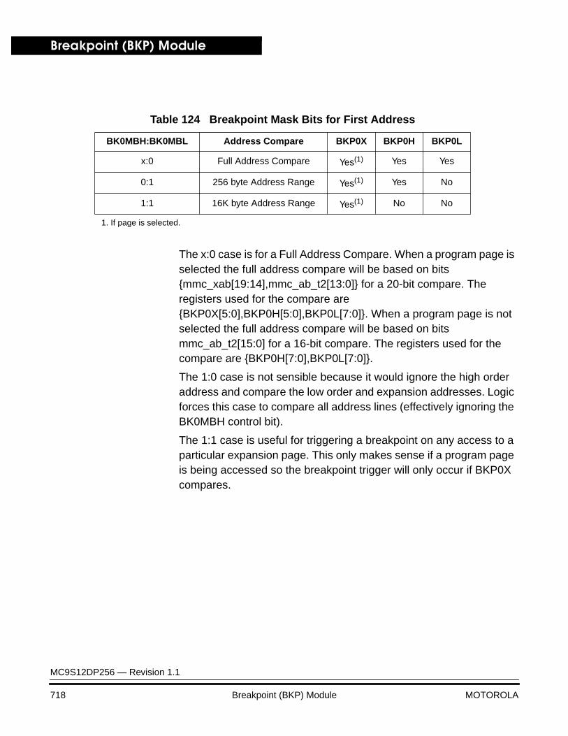
Breakpoint (BKP) Module
MC9S12DP256 — Revision 1.1
718 Breakpoint (BKP) Module MOTOROLA
The x:0 case is for a Full Address Compare. When a program page is selected the full address compare will be based on bits {mmc_xab[19:14],mmc_ab_t2[13:0]} for a 20-bit compare. The registers used for the compare are {BKP0X[5:0],BKP0H[5:0],BKP0L[7:0]}. When a program page is not selected the full address compare will be based on bits mmc_ab_t2[15:0] for a 16-bit compare. The registers used for the compare are {BKP0H[7:0],BKP0L[7:0]}.
The 1:0 case is not sensible because it would ignore the high order address and compare the low order and expansion addresses. Logic forces this case to compare all address lines (effectively ignoring the BK0MBH control bit).
The 1:1 case is useful for triggering a breakpoint on any access to a particular expansion page. This only makes sense if a program page is being accessed so the breakpoint trigger will only occur if BKP0X compares.
Table 124 Breakpoint Mask Bits for First Address
BK0MBH:BK0MBL Address Compare BKP0X BKP0H BKP0L
x:0 Full Address Compare Yes(1) Yes Yes
0:1 256 byte Address Range Yes(1) Yes No
1:1 16K byte Address Range Yes(1) No No
1. If page is selected.
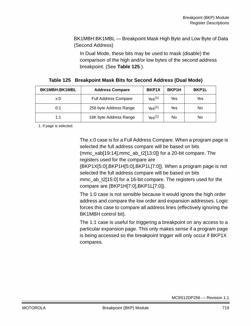
Breakpoint (BKP) ModuleRegister Descriptions
MC9S12DP256 — Revision 1.1
MOTOROLA Breakpoint (BKP) Module 719
BK1MBH:BK1MBL — Breakpoint Mask High Byte and Low Byte of Data (Second Address)
In Dual Mode, these bits may be used to mask (disable) the comparison of the high and/or low bytes of the second address breakpoint. (See Table 125.).
The x:0 case is for a Full Address Compare. When a program page is selected the full address compare will be based on bits {mmc_xab[19:14],mmc_ab_t2[13:0]} for a 20-bit compare. The registers used for the compare are {BKP1X[5:0],BKP1H[5:0],BKP1L[7:0]}. When a program page is not selected the full address compare will be based on bits mmc_ab_t2[15:0] for a 16-bit compare. The registers used for the compare are {BKP1H[7:0],BKP1L[7:0]}.
The 1:0 case is not sensible because it would ignore the high order address and compare the low order and expansion addresses. Logic forces this case to compare all address lines (effectively ignoring the BK1MBH control bit).
The 1:1 case is useful for triggering a breakpoint on any access to a particular expansion page. This only makes sense if a program page is being accessed so the breakpoint trigger will only occur if BKP1X compares.
Table 125 Breakpoint Mask Bits for Second Address (Dual Mode)
BK1MBH:BK1MBL Address Compare BKP1X BKP1H BKP1L
x:0 Full Address Compare Yes(1) Yes Yes
0:1 256 byte Address Range Yes(1) Yes No
1:1 16K byte Address Range Yes(1) No No
1. If page is selected.
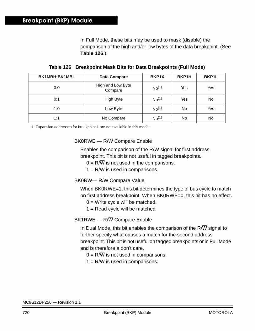
Breakpoint (BKP) Module
MC9S12DP256 — Revision 1.1
720 Breakpoint (BKP) Module MOTOROLA
In Full Mode, these bits may be used to mask (disable) the comparison of the high and/or low bytes of the data breakpoint. (See Table 126.).
BK0RWE — R/W Compare Enable
Enables the comparison of the R/W signal for first address breakpoint. This bit is not useful in tagged breakpoints.
0 = R/W is not used in the comparisons.1 = R/W is used in comparisons.
BK0RW— R/W Compare Value
When BK0RWE=1, this bit determines the type of bus cycle to match on first address breakpoint. When BK0RWE=0, this bit has no effect.
0 = Write cycle will be matched.1 = Read cycle will be matched
BK1RWE — R/W Compare Enable
In Dual Mode, this bit enables the comparison of the R/W signal to further specify what causes a match for the second address breakpoint. This bit is not useful on tagged breakpoints or in Full Mode and is therefore a don’t care.
0 = R/W is not used in comparisons.1 = R/W is used in comparisons.
Table 126 Breakpoint Mask Bits for Data Breakpoints (Full Mode)
BK1MBH:BK1MBL Data Compare BKP1X BKP1H BKP1L
0:0High and Low Byte
Compare No(1) Yes Yes
0:1 High Byte No(1) Yes No
1:0 Low Byte No(1) No Yes
1:1 No Compare No(1) No No
1. Expansion addresses for breakpoint 1 are not available in this mode.
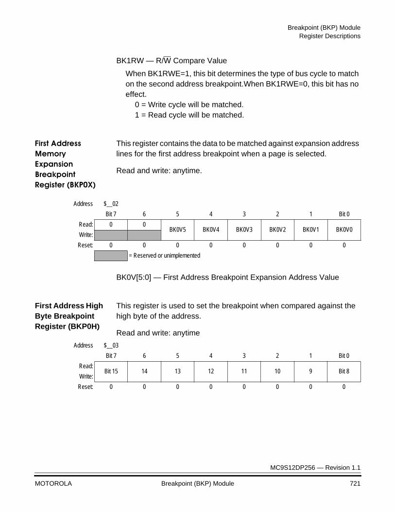
Breakpoint (BKP) ModuleRegister Descriptions
MC9S12DP256 — Revision 1.1
MOTOROLA Breakpoint (BKP) Module 721
BK1RW — R/W Compare Value
When BK1RWE=1, this bit determines the type of bus cycle to match on the second address breakpoint.When BK1RWE=0, this bit has no effect.
0 = Write cycle will be matched.1 = Read cycle will be matched.
First Address Memory Expansion Breakpoint Register (BKP0X)
This register contains the data to be matched against expansion address lines for the first address breakpoint when a page is selected.
Read and write: anytime.
BK0V[5:0] — First Address Breakpoint Expansion Address Value
First Address High Byte Breakpoint Register (BKP0H)
This register is used to set the breakpoint when compared against the high byte of the address.
Read and write: anytime
Address $__02
Bit 7 6 5 4 3 2 1 Bit 0
Read: 0 0BK0V5 BK0V4 BK0V3 BK0V2 BK0V1 BK0V0
Write:
Reset: 0 0 0 0 0 0 0 0
= Reserved or unimplemented
Address $__03
Bit 7 6 5 4 3 2 1 Bit 0
Read:Bit 15 14 13 12 11 10 9 Bit 8
Write:
Reset: 0 0 0 0 0 0 0 0
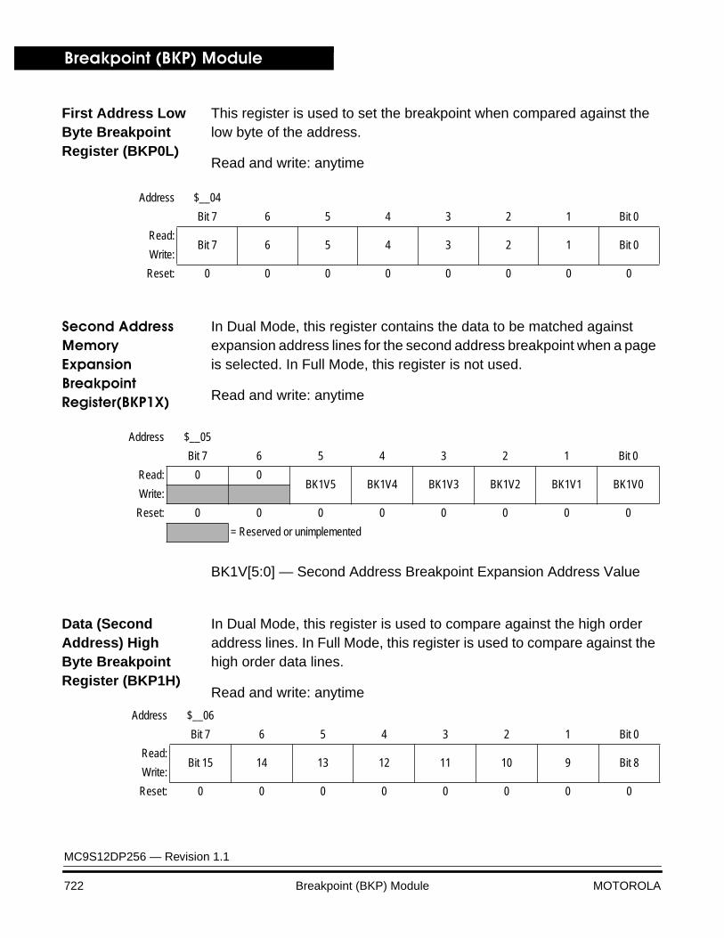
Breakpoint (BKP) Module
MC9S12DP256 — Revision 1.1
722 Breakpoint (BKP) Module MOTOROLA
First Address Low Byte Breakpoint Register (BKP0L)
This register is used to set the breakpoint when compared against the low byte of the address.
Read and write: anytime
Second Address Memory Expansion Breakpoint Register(BKP1X)
In Dual Mode, this register contains the data to be matched against expansion address lines for the second address breakpoint when a page is selected. In Full Mode, this register is not used.
Read and write: anytime
BK1V[5:0] — Second Address Breakpoint Expansion Address Value
Data (Second Address) High Byte Breakpoint Register (BKP1H)
In Dual Mode, this register is used to compare against the high order address lines. In Full Mode, this register is used to compare against the high order data lines.
Read and write: anytime
Address $__04
Bit 7 6 5 4 3 2 1 Bit 0
Read:Bit 7 6 5 4 3 2 1 Bit 0
Write:
Reset: 0 0 0 0 0 0 0 0
Address $__05
Bit 7 6 5 4 3 2 1 Bit 0
Read: 0 0BK1V5 BK1V4 BK1V3 BK1V2 BK1V1 BK1V0
Write:
Reset: 0 0 0 0 0 0 0 0
= Reserved or unimplemented
Address $__06
Bit 7 6 5 4 3 2 1 Bit 0
Read:Bit 15 14 13 12 11 10 9 Bit 8
Write:
Reset: 0 0 0 0 0 0 0 0
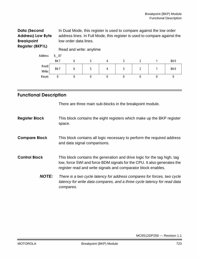
Breakpoint (BKP) ModuleFunctional Description
MC9S12DP256 — Revision 1.1
MOTOROLA Breakpoint (BKP) Module 723
Data (Second Address) Low Byte Breakpoint Register (BKP1L)
In Dual Mode, this register is used to compare against the low order address lines. In Full Mode, this register is used to compare against the low order data lines.
Read and write: anytime
Functional Description
There are three main sub-blocks in the breakpoint module.
Register Block This block contains the eight registers which make up the BKP register space.
Compare Block This block contains all logic necessary to perform the required address and data signal comparisons.
Control Block This block contains the generation and drive logic for the tag high, tag low, force SWI and force BDM signals for the CPU. It also generates the register read and write signals and comparator block enables.
NOTE: There is a two cycle latency for address compares for forces, two cycle latency for write data compares, and a three cycle latency for read data compares.
Address $__07
Bit 7 6 5 4 3 2 1 Bit 0
Read:Bit 7 6 5 4 3 2 1 Bit 0
Write:
Reset: 0 0 0 0 0 0 0 0
Breakpoint (BKP) Module
MC9S12DP256 — Revision 1.1
724 Breakpoint (BKP) Module MOTOROLA
Breakpoint Operating Modes
Dual Address Mode
When Dual Address Mode is enabled, two address breakpoints can be set. Each breakpoint can cause a software interrupt (SWI) or cause the part to enter BDM. The BDM requests have a higher priority than the SWI requests. No data breakpoints are allowed.
The BKTAG bit in the BKPCT0 register selects whether the breakpoint mode is force or tag. The BKxMBH:L bits in the BKPCT1 register select whether or not the breakpoint is matched exactly or is a range breakpoint. They also select whether the address is matched on the high byte, low byte, both bytes, and/or memory expansion. The BKxRW and BKxRWE bits in the BKPCT1 register select whether the type of bus cycle to match is a read, write, or both when performing forced breakpoints.
Full Breakpoint Mode
When in Full Breakpoint Mode, the part enters background debug mode or initiates a software interrupt. The BDM requests have a higher priority than the SWI requests. This mode requires a match on address and data for a breakpoint to occur. R/W matches are also allowed.
The BKTAG bit in the BKPCT0 register selects whether the breakpoint mode is forced or tagged. If the BKTAG bit is set in BKPCT0, then only address is matched, data is ignored. The BK0MBH:L bits in the BKPCT1 register select whether or not the breakpoint is matched exactly, is a range breakpoint, or is in page space. The BK1MBH:L bits in the BKPCT1 register select whether the data is matched on the high byte, low byte, or both bytes. The BK0RW and BK0RWE bits in the BKPCT1 register select whether the type of bus cycle to match is a read or a write when performing forced breakpoints. BK1RW and BK1RWE bits in the BKPCT1 register are not used in Full Mode.
Breakpoint (BKP) ModuleBreakpoint Types
MC9S12DP256 — Revision 1.1
MOTOROLA Breakpoint (BKP) Module 725
Breakpoint Types
The priority of the breakpoint types is as follows. The Breakpoint module gives priority to BDM requests over SWI requests. The external bus interface tags that pass through the BKP module can only assert BDM requests.
SWI During a breakpoint, a signal generated by the breakpoint module is asserted, causing the CPU to execute a SWI instead of the BGND instruction.
BDM Breakpoints are not allowed if the BDM mode is already active. Active mode means the CPU is executing out of the BDM ROM. While in BDM trace mode, tagging into BDM is not allowed.
NOTE: BDM should not be entered from a breakpoint unless the ENABLE bit is set in the BDM. Even if the ENABLE bit in the BDM is negated, the CPU actually executes the BDM ROM code. It checks the ENABLE and returns if enable is not set. If the BDM is not serviced by the monitor, then the breakpoint would be re-asserted when the BDM returns to normal CPU flow.
There is no hardware to enforce restriction of breakpoint operation if the BDM is not enabled.
Modes of Operation
The Breakpoint Module performs the same in all modes of operation.
Table 127 Priority of Forces and Tags
Forces Tags
Force BDM from BDM Module External Bus Interface Tags
Force BDM from BKP Module Breakpoint Module Tags
Breakpoint (BKP) Module
MC9S12DP256 — Revision 1.1
726 Breakpoint (BKP) Module MOTOROLA
Low Power Options
Low power options are available in the BKP sub-block.
Run Mode In run mode, if BKEN=0, all clocks to the breakpoint system are disabled.
Wait Mode Wait mode power savings can be achieved by having the clock generator shut down the core clock if the BDM is not used.
Stop Mode The BKP sub-block will be completely shutdown during a STOP instruction.
Reset Initialization
The reset state of each individual bit is listed within the Register Description section, which details the registers and their bit-fields. All registers are reset by the system reset.
Interrupt Operation
The BKP sub-block causes the CPU to generate SWI interrupts when BKBDM bit is equal to zero.
General Purpose I/O Ports
The BKP sub-block does not include any general purpose I/O ports.

MC9S12DP256 — Revision 1.1
MOTOROLA Revision History 727
Revision HistoryRevision History
This section lists the revision history of the document since Rev 1.0 (the first general release). Data for previous revisions is unavailable.
Changes from Rev 1.0 to Rev 1.1
Section Page (in Rev 1.1) Description of change
General Description various Notes about 80-pin version of device added
Pinout and Signal Description
various Notes about 80-pin version of device added
Pinout and Signal Description
54Table 7:Pin 46 corrected from XTAL to EXTAL
Pinout and Signal Description
54Table 7:Pin 47 corrected from EXTAL to XTAL
Pinout and Signal Description
55Table 7:Pin 68 corrected from PAD10/AN08 to PAD08/AN08

Revision History
MC9S12DP256 — Revision 1.1
728 Revision History MOTOROLA
MC9S12DP256 — Revision 1.1
MOTOROLA Glossary 729
GlossaryGlossary
A — See “accumulators (A and B or D).”
accumulators (A and B or D) — Two 8-bit (A and B) or one 16-bit (D) general-purpose registers in the CPU. The CPU uses the accumulators to hold operands and results of arithmetic and logic operations.
acquisition mode — A mode of PLL operation with large loop bandwidth. Also see ’tracking mode’.
address bus — The set of wires that the CPU or DMA uses to read and write memory locations.
addressing mode — The way that the CPU determines the operand address for an instruction. The M68HC12 CPU has 15 addressing modes.
ALU — See “arithmetic logic unit (ALU).”
analogue-to-digital converter (ATD) — The ATD module is an 8-channel, multiplexed-input successive-approximation analog-to-digital converter.
arithmetic logic unit (ALU) — The portion of the CPU that contains the logic circuitry to perform arithmetic, logic, and manipulation operations on operands.
asynchronous — Refers to logic circuits and operations that are not synchronized by a common reference signal.
ATD — See “analogue-to-digital converter”.
Glossary
MC9S12DP256 — Revision 1.1
730 Glossary MOTOROLA
B — See “accumulators (A and B or D).”
baud rate — The total number of bits transmitted per unit of time.
BCD — See “binary-coded decimal (BCD).”
binary — Relating to the base 2 number system.
binary number system — The base 2 number system, having two digits, 0 and 1. Binary arithmetic is convenient in digital circuit design because digital circuits have two permissible voltage levels, low and high. The binary digits 0 and 1 can be interpreted to correspond to the two digital voltage levels.
binary-coded decimal (BCD) — A notation that uses 4-bit binary numbers to represent the 10 decimal digits and that retains the same positional structure of a decimal number. For example,
234 (decimal) = 0010 0011 0100 (BCD)
bit — A binary digit. A bit has a value of either logic 0 or logic 1.
branch instruction — An instruction that causes the CPU to continue processing at a memory location other than the next sequential address.
break module — The break module allows software to halt program execution at a programmable point in order to enter a background routine.
breakpoint — A number written into the break address registers of the break module. When a number appears on the internal address bus that is the same as the number in the break address registers, the CPU executes the software interrupt instruction (SWI).
Glossary
MC9S12DP256 — Revision 1.1
MOTOROLA Glossary 731
break interrupt — A software interrupt caused by the appearance on the internal address bus of the same value that is written in the break address registers.
bus — A set of wires that transfers logic signals.
bus clock — See "CPU clock".
byte — A set of eight bits.
CAN — See "Motorola scalable CAN."
CCR — See “condition code register.”
central processor unit (CPU) — The primary functioning unit of any computer system. The CPU controls the execution of instructions.
CGM — See “clock generator module (CGM).”
clear — To change a bit from logic 1 to logic 0; the opposite of set.
clock — A square wave signal used to synchronize events in a computer.
clock generator module (CGM) — The CGM module generates a base clock signal from which the system clocks are derived. The CGM may include a crystal oscillator circuit and/or phase-locked loop (PLL) circuit.
comparator — A device that compares the magnitude of two inputs. A digital comparator defines the equality or relative differences between two binary numbers.
computer operating properly module (COP) — A counter module that resets the MCU if allowed to overflow.
Glossary
MC9S12DP256 — Revision 1.1
732 Glossary MOTOROLA
condition code register (CCR) — An 8-bit register in the CPU that contains the interrupt mask bit and five bits that indicate the results of the instruction just executed.
control bit — One bit of a register manipulated by software to control the operation of the module.
control unit — One of two major units of the CPU. The control unit contains logic functions that synchronize the machine and direct various operations. The control unit decodes instructions and generates the internal control signals that perform the requested operations. The outputs of the control unit drive the execution unit, which contains the arithmetic logic unit (ALU), CPU registers, and bus interface.
COP — See "computer operating properly module (COP)."
CPU — See “central processor unit (CPU).”
CPU12 — The CPU of the MC68HC12 Family.
CPU clock — Bus clock select bits BCSP and BCSS in the clock select register (CLKSEL) determine which clock drives SYSCLK for the main system, including the CPU and buses. When EXTALi drives the SYSCLK, the CPU or bus clock frequency (fo) is equal to the EXTALi frequency divided by 2.
CPU cycles — A CPU cycle is one period of the internal bus clock, normally derived by dividing a crystal oscillator source by two or more so the high and low times will be equal. The length of time required to execute an instruction is measured in CPU clock cycles.
Glossary
MC9S12DP256 — Revision 1.1
MOTOROLA Glossary 733
CPU registers — Memory locations that are wired directly into the CPU logic instead of being part of the addressable memory map. The CPU always has direct access to the information in these registers. The CPU registers in an M68HC12 are:
• A (8-bit accumulator)
• B (8-bit accumulator)
– D (16-bit accumulator formed by concatenation of accumulators A and B)
• IX (16-bit index register)
• IY (16-bit index register)
• SP (16-bit stack pointer)
• PC (16-bit program counter)
• CCR (8-bit condition code register)
cycle time — The period of the operating frequency: tCYC = 1/fOP.
D — See “accumulators (A and B or D).”
decimal number system — Base 10 numbering system that uses the digits zero through nine.
duty cycle — A ratio of the amount of time the signal is on versus the time it is off. Duty cycle is usually represented by a percentage.
ECT — See “enhanced capture timer.”
EEPROM — Electrically erasable, programmable, read-only memory. A nonvolatile type of memory that can be electrically erased and reprogrammed.
Glossary
MC9S12DP256 — Revision 1.1
734 Glossary MOTOROLA
EPROM — Erasable, programmable, read-only memory. A nonvolatile type of memory that can be erased by exposure to an ultraviolet light source and then reprogrammed.
enhanced capture timer (ECT) — The HC12 Enhanced Capture Timer module has the features of the HC12 Standard Timer module enhanced by additional features in order to enlarge the field of applications.
exception — An event such as an interrupt or a reset that stops the sequential execution of the instructions in the main program.
fetch — To copy data from a memory location into the accumulator.
firmware — Instructions and data programmed into nonvolatile memory.
flash EEPROM — Electrically erasable, programmable, read-only memory. A nonvolatile type of memory that can be electrically erased and reprogrammed. Does not support byte or word erase.
free-running counter — A device that counts from zero to a predetermined number, then rolls over to zero and begins counting again.
full-duplex transmission — Communication on a channel in which data can be sent and received simultaneously.
Glossary
MC9S12DP256 — Revision 1.1
MOTOROLA Glossary 735
hexadecimal — Base 16 numbering system that uses the digits 0 through 9 and the letters A through F.
high byte — The most significant eight bits of a word.
illegal address — An address not within the memory map
illegal opcode — A nonexistent opcode.
index registers (IX and IY) — Two 16-bit registers in the CPU. In the indexed addressing modes, the CPU uses the contents of IX or IY to determine the effective address of the operand. IX and IY can also serve as a temporary data storage locations.
input/output (I/O) — Input/output interfaces between a computer system and the external world. A CPU reads an input to sense the level of an external signal and writes to an output to change the level on an external signal.
instructions — Operations that a CPU can perform. Instructions are expressed by programmers as assembly language mnemonics. A CPU interprets an opcode and its associated operand(s) and instruction.
interrupt — A temporary break in the sequential execution of a program to respond to signals from peripheral devices by executing a subroutine.
interrupt request — A signal from a peripheral to the CPU intended to cause the CPU to execute a subroutine.
I/O — See “input/output (I/0).”
jitter — Short-term signal instability.
Glossary
MC9S12DP256 — Revision 1.1
736 Glossary MOTOROLA
latch — A circuit that retains the voltage level (logic 1 or logic 0) written to it for as long as power is applied to the circuit.
latency — The time lag between instruction completion and data movement.
least significant bit (LSB) — The rightmost digit of a binary number.
logic 1 — A voltage level approximately equal to the input power voltage (VDD).
logic 0 — A voltage level approximately equal to the ground voltage (VSS).
low byte — The least significant eight bits of a word.
M68HC12 — A Motorola family of 16-bit MCUs.
mark/space — The logic 1/logic 0 convention used in formatting data in serial communication.
mask — 1. A logic circuit that forces a bit or group of bits to a desired state. 2. A photomask used in integrated circuit fabrication to transfer an image onto silicon.
MCU — Microcontroller unit. See “microcontroller.”
Glossary
MC9S12DP256 — Revision 1.1
MOTOROLA Glossary 737
memory location — Each M68HC12 memory location holds one byte of data and has a unique address. To store information in a memory location, the CPU places the address of the location on the address bus, the data information on the data bus, and asserts the write signal. To read information from a memory location, the CPU places the address of the location on the address bus and asserts the read signal. In response to the read signal, the selected memory location places its data onto the data bus.
memory map — A pictorial representation of all memory locations in a computer system.
MI-Bus — See "Motorola interconnect bus".
microcontroller — Microcontroller unit (MCU). A complete computer system, including a CPU, memory, a clock oscillator, and input/output (I/O) on a single integrated circuit.
modulo counter — A counter that can be programmed to count to any number from zero to its maximum possible modulus.
most significant bit (MSB) — The leftmost digit of a binary number.
Motorola interconnect bus (MI-Bus) — The Motorola Interconnect Bus (MI Bus) is a serial communications protocol which supports distributed real-time control efficiently and with a high degree of noise immunity.
Motorola scalable CAN (msCAN) — The Motorola scalable controller area network is a serial communications protocol that efficiently supports distributed real-time control with a very high level of data integrity.
msCAN — See "Motorola scalable CAN".
Glossary
MC9S12DP256 — Revision 1.1
738 Glossary MOTOROLA
MSI — See "multiple serial interface".
multiple serial interface — A module consisting of multiple independent serial I/O sub-systems, e.g. two SCI and one SPI.
multiplexer — A device that can select one of a number of inputs and pass the logic level of that input on to the output.
nibble — A set of four bits (half of a byte).
object code — The output from an assembler or compiler that is itself executable machine code, or is suitable for processing to produce executable machine code.
opcode — A binary code that instructs the CPU to perform an operation.
open-drain — An output that has no pullup transistor. An external pullup device can be connected to the power supply to provide the logic 1 output voltage.
operand — Data on which an operation is performed. Usually a statement consists of an operator and an operand. For example, the operator may be an add instruction, and the operand may be the quantity to be added.
oscillator — A circuit that produces a constant frequency square wave that is used by the computer as a timing and sequencing reference.
OTPROM — One-time programmable read-only memory. A nonvolatile type of memory that cannot be reprogrammed.
Glossary
MC9S12DP256 — Revision 1.1
MOTOROLA Glossary 739
overflow — A quantity that is too large to be contained in one byte or one word.
page zero — The first 256 bytes of memory (addresses $0000–$00FF).
parity — An error-checking scheme that counts the number of logic 1s in each byte transmitted. In a system that uses odd parity, every byte is expected to have an odd number of logic 1s. In an even parity system, every byte should have an even number of logic 1s. In the transmitter, a parity generator appends an extra bit to each byte to make the number of logic 1s odd for odd parity or even for even parity. A parity checker in the receiver counts the number of logic 1s in each byte. The parity checker generates an error signal if it finds a byte with an incorrect number of logic 1s.
PC — See “program counter (PC).”
peripheral — A circuit not under direct CPU control.
phase-locked loop (PLL) — A clock generator circuit in which a voltage controlled oscillator produces an oscillation which is synchronized to a reference signal.
PLL — See "phase-locked loop (PLL)."
pointer — Pointer register. An index register is sometimes called a pointer register because its contents are used in the calculation of the address of an operand, and therefore points to the operand.
Glossary
MC9S12DP256 — Revision 1.1
740 Glossary MOTOROLA
polarity — The two opposite logic levels, logic 1 and logic 0, which correspond to two different voltage levels, VDD and VSS.
polling — Periodically reading a status bit to monitor the condition of a peripheral device.
port — A set of wires for communicating with off-chip devices.
prescaler — A circuit that generates an output signal related to the input signal by a fractional scale factor such as 1/2, 1/8, 1/10 etc.
program — A set of computer instructions that cause a computer to perform a desired operation or operations.
program counter (PC) — A 16-bit register in the CPU. The PC register holds the address of the next instruction or operand that the CPU will use.
pull — An instruction that copies into the accumulator the contents of a stack RAM location. The stack RAM address is in the stack pointer.
pullup — A transistor in the output of a logic gate that connects the output to the logic 1 voltage of the power supply.
pulse-width — The amount of time a signal is on as opposed to being in its off state.
pulse-width modulation (PWM) — Controlled variation (modulation) of the pulse width of a signal with a constant frequency.
push — An instruction that copies the contents of the accumulator to the stack RAM. The stack RAM address is in the stack pointer.
PWM period — The time required for one complete cycle of a PWM waveform.
Glossary
MC9S12DP256 — Revision 1.1
MOTOROLA Glossary 741
RAM — Random access memory. All RAM locations can be read or written by the CPU. The contents of a RAM memory location remain valid until the CPU writes a different value or until power is turned off.
RC circuit — A circuit consisting of capacitors and resistors having a defined time constant.
read — To copy the contents of a memory location to the accumulator.
register — A circuit that stores a group of bits.
reserved memory location — A memory location that is used only in special factory test modes. Writing to a reserved location has no effect. Reading a reserved location returns an unpredictable value.
reset — To force a device to a known condition.
ROM — Read-only memory. A type of memory that can be read but cannot be changed (written). The contents of ROM must be specified before manufacturing the MCU.
SCI — See "serial communication interface module (SCI)."
serial — Pertaining to sequential transmission over a single line.
serial communications interface module (SCI) — A module that supports asynchronous communication.
serial peripheral interface module (SPI) — A module that supports synchronous communication.
Glossary
MC9S12DP256 — Revision 1.1
742 Glossary MOTOROLA
set — To change a bit from logic 0 to logic 1; opposite of clear.
shift register — A chain of circuits that can retain the logic levels (logic 1 or logic 0) written to them and that can shift the logic levels to the right or left through adjacent circuits in the chain.
signed — A binary number notation that accommodates both positive and negative numbers. The most significant bit is used to indicate whether the number is positive or negative, normally logic 0 for positive and logic 1 for negative. The other seven bits indicate the magnitude of the number.
software — Instructions and data that control the operation of a microcontroller.
software interrupt (SWI) — An instruction that causes an interrupt and its associated vector fetch.
SPI — See "serial peripheral interface module (SPI)."
stack — A portion of RAM reserved for storage of CPU register contents and subroutine return addresses.
stack pointer (SP) — A 16-bit register in the CPU containing the address of the next available storage location on the stack.
start bit — A bit that signals the beginning of an asynchronous serial transmission.
status bit — A register bit that indicates the condition of a device.

Glossary
MC9S12DP256 — Revision 1.1
MOTOROLA Glossary 743
stop bit — A bit that signals the end of an asynchronous serial transmission.
subroutine — A sequence of instructions to be used more than once in the course of a program. The last instruction in a subroutine is a return from subroutine (RTS) instruction. At each place in the main program where the subroutine instructions are needed, a jump or branch to subroutine (JSR or BSR) instruction is used to call the subroutine. The CPU leaves the flow of the main program to execute the instructions in the subroutine. When the RTS instruction is executed, the CPU returns to the main program where it left off.
synchronous — Refers to logic circuits and operations that are synchronized by a common reference signal.
timer — A module used to relate events in a system to a point in time.
toggle — To change the state of an output from a logic 0 to a logic 1 or from a logic 1 to a logic 0.
tracking mode — A mode of PLL operation with narrow loop bandwidth. Also see ‘acquisition mode.’
two’s complement — A means of performing binary subtraction using addition techniques. The most significant bit of a two’s complement number indicates the sign of the number (1 indicates negative). The two’s complement negative of a number is obtained by inverting each bit in the number and then adding 1 to the result.
unbuffered — Utilizes only one register for data; new data overwrites current data.
unimplemented memory location — A memory location that is not used. Writing to an unimplemented location has no effect. Reading an unimplemented location returns an unpredictable value.

Glossary
MC9S12DP256 — Revision 1.1
744 Glossary MOTOROLA
variable — A value that changes during the course of program execution.
VCO — See "voltage-controlled oscillator."
vector — A memory location that contains the address of the beginning of a subroutine written to service an interrupt or reset.
voltage-controlled oscillator (VCO) — A circuit that produces an oscillating output signal of a frequency that is controlled by a dc voltage applied to a control input.
waveform — A graphical representation in which the amplitude of a wave is plotted against time.
wired-OR — Connection of circuit outputs so that if any output is high, the connection point is high.
word — A set of two bytes (16 bits).
write — The transfer of a byte of data from the CPU to a memory location.
MC9S12DP256 — Revision 1.1
MOTOROLA Literature Updates 745
Literature UpdatesLiterature Updates
This document contains the latest data available at publication time. For updates, contact one of the centers listed below:
Literature Distribution Centers
Order literature by mail or phone.
USA/Europe Motorola Literature DistributionP.O. Box 5405Denver, Colorado, 80217Phone 1-303-675-2140
Japan Motorola Japan Ltd.Tatsumi-SPD-JLDCToshikatsu Otsuki6F Seibu-Butsuryu Center3-14-2 Tatsumi Koto-KuTokyo 135, JapanPhone 03-3521-8315
Hong Kong Motorola Semiconductors H.K. Ltd.8B Tai Ping Industrial Park51 Ting Kok RoadTai Po, N.T., Hong KongPhone 852-26629298
Literature Updates
MC9S12DP256 — Revision 1.1
746 Literature Updates MOTOROLA
Customer Focus Center
1-800-521-6274
Microcontroller DivisionÕs Web Site
Directly access the Microcontroller Division’s web site with the following URL:
http://www.motorola.com/semiconductors

2
1
3
4
5
6
7
8
9
10
11
12
13
14
15
2
1
3
4
5
6
7
8
9
0
1
2
3
4
5
Motorola reserves the right to make changes without further notice to any products herein. Motorola makes no warranty, representation or guarantee regarding thesuitability of its products for any particular purpose, nor does Motorola assume any liability arising out of the application or use of any product or circuit, andspecifically disclaims any and all liability, including without limitation consequential or incidental damages. "Typical" parameters which may be provided in Motoroladata sheets and/or specifications can and do vary in different applications and actual performance may vary over time. All operating parameters, including "Typicals"must be validated for each customer application by customer's technical experts. Motorola does not convey any license under its patent rights nor the rights ofothers. Motorola products are not designed, intended, or authorized for use as components in systems intended for surgical implant into the body, or otherapplications intended to support or sustain life, or for any other application in which the failure of the Motorola product could create a situation where personal injuryor death may occur. Should Buyer purchase or use Motorola products for any such unintended or unauthorized application, Buyer shall indemnify and hold Motorolaand its officers, employees, subsidiaries, affiliates, and distributors harmless against all claims, costs, damages, and expenses, and reasonable attorney fees arisingout of, directly or indirectly, any claim of personal injury or death associated with such unintended or unauthorized use, even if such claim alleges that Motorola wasnegligent regarding the design or manufacture of the part. Motorola and are registered trademarks of Motorola, Inc. Motorola, Inc. is an EqualOpportunity/Affirmative Action Employer.
How to reach us:USA/EUROPE: Motorola Literature Distribution; P.O. Box 5405, Denver, Colorado 80217. 1-303-675-2140
HOME PAGE: http://motorola.com/sps/JAPAN: Motorola Japan Ltd.; SPS, Technial Information Center, 3-20-1, Minami-Azabu, Minato-ku, Tokyo 106-8573 Japan.
81-3-3440-3569ASIA/PACIFIC: Motorola Semiconductors H.K. Ltd.; Silicon Harbour Centre, 2 Dai King Street, Tai Po Industrial Estate,
Tai Po, N.T., Hong Kong. 852-266668334CUSTOMER FOCUS CENTER: 1-800-521-6274
© Motorola, Inc., 2000
MC9S12DP256/D

![Untitled Document [] · 2001-04-08 · – Upward compatible with M68HC11 instruction set – Interrupt stacking and programmer’s model identical to M68HC11 – 20-bit ALU – Instruction](https://static.documents.pub/doc/80x56/5e8a5d84ae965315236ff2fb/untitled-document-2001-04-08-a-upward-compatible-with-m68hc11-instruction.jpg)


