96-Channel Bidirectional Digital Input Module Reference Design for PLC
TI Designs: TIDA-06001496-Channel Bidirectional Digital Input Module ReferenceDesign for PLC
DescriptionThis reference design is a compact implementation of96 isolated digital input channels using the ISO1212device which is an isolated digital input receiver. Thisdesign shows the current limit feature of the ISO1212device which has better thermal performance thantraditional optocoupler solutions. This design makes adigital input board with multiple channels morecompact and decreases board temperature (less than50). A MUX and decoder with the ISO1212 devicedecreases the number of pins of the microcontrollerfrom 96 to 8. The design was tested with 100-kHzinput signals (200 kbit) per channel. The design usesless than 7.3 W of input power which results in lessheat dissipation. All signals are designed to withstandESD, EFT, and surge events according to IEC6100-4.
Features• 96-channel bidirectional digital input module• Voltage Inputs: 24-VDC Range, Limited to 3.1 mA
Per Channel• Compact and Low Temperature Rise Design (<
50 at 1 hour With All 96 Channels On)• Small Board Size, Core Board Size of 65 × 70 mm2
• Serial Output Option• Tested to 0.5-kV Surge (IEC61000-4-5, 42 Ω),
Scalable to 1 kV With Enhancements• Header for LaunchPad™ Development Kit for
Quick and Easy Evaluation
Applications• Programmable Logic Controllers and Digital Input
Modules• Distributed Control Systems• Computer Numerical Control• Railway Signaling Data Loggers
An IMPORTANT NOTICE at the end of this TI reference design addresses authorized use, intellectual property matters and otherimportant disclaimers and information.
96-Channel Bidirectional Digital Input Module Reference Design for PLC
1 System DescriptionThis reference design is a compact implementation of 96 isolated bidirectional digital input channels usingTI's ISO1212 device. The ISO1212 device is a dual-channel isolated 24-V digital-input receiver for a digitalinput (DI) module with programmable logic controller (PLC) . The ISO1212 device has an accurate currentlimit to enable a more compact and high-density DI board design.
The 96 channels are divided into 6 groups of 16 channels. Each channel has 8 dual-channel ISO1212devices. A MUX and decoder are used to read the output states of the 96 channels. The MUX anddecoder with the output-enable function of the ISO1212 device decrease the number of pins of themicrocontroller 96 to 8. The serials outputs of the MUX can be read out using any I/O pin on themicrocontroller. A TI LaunchPad™ development kit detects the state of each channel and supplies powerto the system.
The design was tested by using 100-kHz input signals (200-kbit) per channel. However, the ISO121xdevices support data rates of up to 4 Mbps and can be used in a faster signal system. The design usesless than 7.3 W of input power which results in less heat dissipation. Each channel was designed towithstand surge (IEC 61000-4-5), ESD (IEC 61000-4-2) and EFT (IEC 61000-4-4) test. An RC low-passfilter was used for the surge test.
1.1 Key System Specifications
Table 1. Key System Specifications
PARAMETER SPECIFICATIONS DETAILSNumber of channels 96 in groups of 16 —High level threshold voltage (VIH) 15.34 V Section 2.3.1Low level threshold voltage (VIL) 14.39 V Section 2.3.1I(IN+SENSEx), typical sum of current drawnfrom the IN and SENSE pins 3.1 mA/per channel Section 2.3.1
Power consumption 7.3 W for 96 channels, 24-V VIN Section 3.2.2.2
Thermal dissipation 40°C maximum after 1 hour of continuous operation, 24-V VIN,25°C ambient temperature Section 3.2.2.2
Total time to read output states 125.2 µs, reading 96 channels one time Section 3.2.2.4
96-Channel Bidirectional Digital Input Module Reference Design for PLC
2.2 Highlighted Products
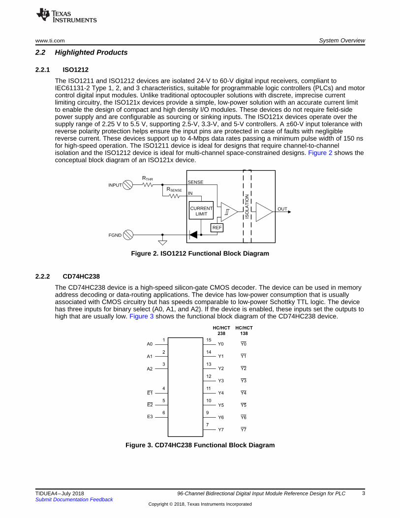
2.2.1 ISO1212The ISO1211 and ISO1212 devices are isolated 24-V to 60-V digital input receivers, compliant toIEC61131-2 Type 1, 2, and 3 characteristics, suitable for programmable logic controllers (PLCs) and motorcontrol digital input modules. Unlike traditional optocoupler solutions with discrete, imprecise currentlimiting circuitry, the ISO121x devices provide a simple, low-power solution with an accurate current limitto enable the design of compact and high density I/O modules. These devices do not require field-sidepower supply and are configurable as sourcing or sinking inputs. The ISO121x devices operate over thesupply range of 2.25 V to 5.5 V, supporting 2.5-V, 3.3-V, and 5-V controllers. A ±60-V input tolerance withreverse polarity protection helps ensure the input pins are protected in case of faults with negligiblereverse current. These devices support up to 4-Mbps data rates passing a minimum pulse width of 150 nsfor high-speed operation. The ISO1211 device is ideal for designs that require channel-to-channelisolation and the ISO1212 device is ideal for multi-channel space-constrained designs. Figure 2 shows theconceptual block diagram of an ISO121x device.
Figure 2. ISO1212 Functional Block Diagram
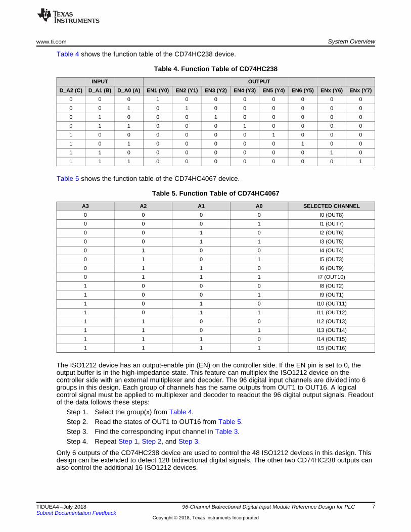
2.2.2 CD74HC238The CD74HC238 device is a high-speed silicon-gate CMOS decoder. The device can be used in memoryaddress decoding or data-routing applications. The device has low-power consumption that is usuallyassociated with CMOS circuitry but has speeds comparable to low-power Schottky TTL logic. The devicehas three inputs for binary select (A0, A1, and A2). If the device is enabled, these inputs set the outputs tohigh that are usually low. Figure 3 shows the functional block diagram of the CD74HC238 device.
96-Channel Bidirectional Digital Input Module Reference Design for PLC
2.2.3 CD74HC4067The CD74HC4067 device is digitally controlled analog switches that utilize silicon-gate CMOS technologyto achieve operating speeds similar to LSTTL, with the low power consumption of standard CMOSintegrated circuits. They are bidirectional switches thus allowing any analog input to be used as an outputand vice-versa. The switches have low on resistance and low off leakages. In addition, these devices havean enable control which when high will disable all switches to their off state. Figure 4 shows theconceptual block diagram of CD74HC4067 device.
Figure 4. CD74HC4067 Functional Block Diagram
2.3 System Design Theory
2.3.1 Digital Input StageThe 96 bidirectional inputs go into 48 ISO1212 devices. Figure 5 shows the input stages of one ISO1212device with two input signals.
96-Channel Bidirectional Digital Input Module Reference Design for PLC
The input stage uses the rectifier and then the ISO1212 device. Each device can detect two bidirectionalsignals. The diodes of the rectifier must meet these specifications to rectify the bidirectional signal:• VR > VLINE(max)
where:– VR is the reverse voltage.– VLINE(max) is the line voltage.
• IF > I(IN+SENSE)
where:– IF is the forward current.– I(IN+SENSE) is the typical sum of current drwan from the IN and SENSE pins.
This design is for the PLC DI board, BAS70XY with an IF current of 200 mA and VR voltage of 70 V. TheBAS70XY board was selected because of the maximum line voltage and current limit. The COM pin inFigure 5 is the common field ground for all digital inputs.
The ISO1212 device is a fully-integrated, isolated digital-input receiver with IEC 61131-2 Type 1, Type 2,and Type 3 characteristics. The RSENSE resistor on the input signal path precisely sets the limit for thecurrent drawn from the field input to be set for Type 1, Type 2, or Type 3 operation. The RTHR resistor setsthe voltage thresholds and limits limit the surge current. An input capacitor, CIN, is connected between theRTHR resistor and COM pin. The RTHR resistor to COM pin creates an RC filter for additional protectionfrom ESD, EFT, and surge events. Table 2 shows the configurations for Type 1 and Type 3 digital inputs.Table 2 also shows the voltage rating results for the specific values of RTHR, RSENSE, and CIN according toIEC 61002-4-2, IEC 61002-4-4, and IEC 61002-4-5, respectively.
Type 3 562 Ω 1 kΩ10 nF ±1 kV ±1 kV ±500 V ±6 kV ±4 kV
330 nF ±1 kV ±1 kV ±1 kV ±6 kV ±4 kV
All channels in this design are configured for Type 1 inputs. The RSENSE resistor has a value of 280 Ω. TheRTHR resistor has a value of 1.8 kΩ. The CIN capacitor has a value of 470 pF to filter the input surge pulsefurther. Use Equation 1 to calculate the typical current limit (IL). Use Equation 2 to calculate the typicalhigh-level threshold (VIH(typ)), Use Equation 2 to calculate the minimum low-level threshold (VIL(typ)).Equation 1, Equation 2, and Equation 2 calculate the values at the ISO1212 input (including RTHR) for thehigh-level output high and low-level output.
IL = (2.25 mA × 562 Ω) / RSENSE = 3.1 mA (1)VIH(typ) = 8.25 V + RTHR × (2.25 mA × 562 Ω) / RSENSE + 2 × VD = 15.34 V (2)VIL(typ) = 7.1 V + RTHR × (2.25 mA × 562 Ω) / RSENSE + 2 × VD = 14.19 V (3)
The ISO1212 device has an output-enable pin (EN) on the controller side. If the EN pin is set to 0, theoutput buffer is in the high-impedance state. This feature can multiplex the ISO1212 device on thecontroller side with an external multiplexer and decoder. The 96 digital input channels are divided into 6groups in this design. Each group of channels has the same outputs from OUT1 to OUT16. A logicalcontrol signal must be applied to multiplexer and decoder to readout the 96 digital output signals. Readoutof the data follows these steps:
Step 1. Select the group(x) from Table 4.Step 2. Read the states of OUT1 to OUT16 from Table 5.Step 3. Find the corresponding input channel in Table 3.Step 4. Repeat Step 1, Step 2, and Step 3.
Only 6 outputs of the CD74HC238 device are used to control the 48 ISO1212 devices in this design. Thisdesign can be extended to detect 128 bidirectional digital signals. The other two CD74HC238 outputs canalso control the additional 16 ISO1212 devices.
96-Channel Bidirectional Digital Input Module Reference Design for PLC
2.3.3 Floor Plan DiagramPut the ISO1212 device on the bottom and top layer for a more compact design. Measure externalspacing in clearance to pass safety standards. The shortest terminal-to-terminal distance through air of theISO1212 device is 3.7 mm. Figure 6 shows the design solution.
(1) M = 4 units, N = 6 units
Figure 6. Floor Plan Design of Multichannel DI Board
The design has a symmetrical layout and the shape of this design more square than is shown. The layoutof the design has two basic advantages. The first advantage is that this design is more common in mostapplications. The second advantage is that this design decreases the clearance between the field sidesignal and MCU side signal. Signal 1 in Figure 6 must be the MCU side signal to decrease the clearance.Use these methods to make this board more compact:• Decrease the decoupling capacitance on the VCC1 side (signal 2 in Figure 6). Only 4 decoupling
capacitors are needed for the 8 ISO1212 device in this zone.• Use more internal layers when routing the signal.• Use symmetrical layout when routing the signal. If the output signals are multiplexed, give the outputs
of the ISO1212 device on the bottom and top layers the same nets. Use vias to connect these nets todecrease the board size more.
96-Channel Bidirectional Digital Input Module Reference Design for PLC
3 Hardware, Software, Testing Requirements and Test Results
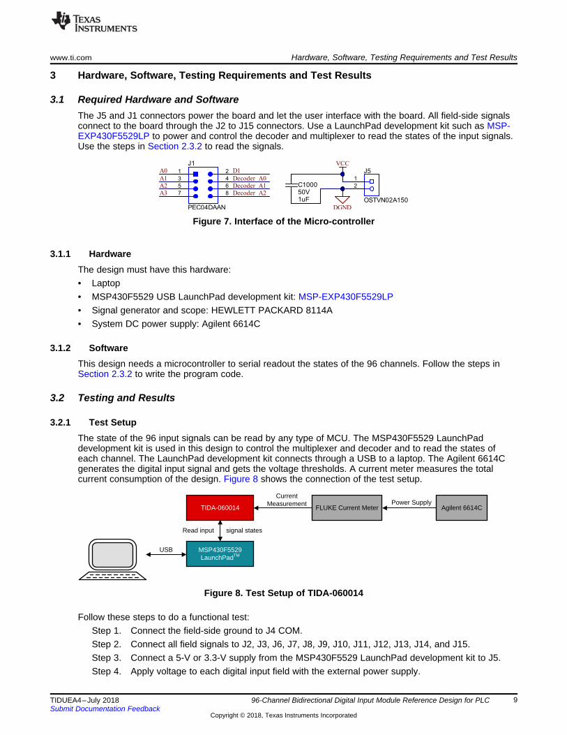
3.1 Required Hardware and SoftwareThe J5 and J1 connectors power the board and let the user interface with the board. All field-side signalsconnect to the board through the J2 to J15 connectors. Use a LaunchPad development kit such as MSP-EXP430F5529LP to power and control the decoder and multiplexer to read the states of the input signals.Use the steps in Section 2.3.2 to read the signals.
Figure 7. Interface of the Micro-controller
3.1.1 HardwareThe design must have this hardware:• Laptop• MSP430F5529 USB LaunchPad development kit: MSP-EXP430F5529LP• Signal generator and scope: HEWLETT PACKARD 8114A• System DC power supply: Agilent 6614C
3.1.2 SoftwareThis design needs a microcontroller to serial readout the states of the 96 channels. Follow the steps inSection 2.3.2 to write the program code.
3.2 Testing and Results
3.2.1 Test SetupThe state of the 96 input signals can be read by any type of MCU. The MSP430F5529 LaunchPaddevelopment kit is used in this design to control the multiplexer and decoder and to read the states ofeach channel. The LaunchPad development kit connects through a USB to a laptop. The Agilent 6614Cgenerates the digital input signal and gets the voltage thresholds. A current meter measures the totalcurrent consumption of the design. Figure 8 shows the connection of the test setup.
Figure 8. Test Setup of TIDA-060014
Follow these steps to do a functional test:Step 1. Connect the field-side ground to J4 COM.Step 2. Connect all field signals to J2, J3, J6, J7, J8, J9, J10, J11, J12, J13, J14, and J15.Step 3. Connect a 5-V or 3.3-V supply from the MSP430F5529 LaunchPad development kit to J5.Step 4. Apply voltage to each digital input field with the external power supply.
96-Channel Bidirectional Digital Input Module Reference Design for PLC
Step 5. Adjust the DC level to find the VIL and VIH hysteresis of the field inputs.Step 6. Program the MSP430F5529 LaunchPad development kit.Step 7. Apply the control signal to J1.Step 8. Apply the group control signal to DecoderA0 through DecoderA3 to select the group number.Step 9. Apply the control signal to the channels to select the channel number and store the value
according to Table 3 to Table 5.
3.2.2 Test Results
3.2.2.1 Functional TestThe test results show that the performance of the digital input module is as expected. This section givesthe test results to reference for this design.
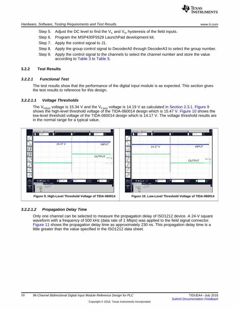
3.2.2.1.1 Voltage ThresholdsThe VIH(typ) voltage is 15.34 V and the VIL(typ) voltage is 14.19 V as calculated in Section 2.3.1. Figure 9shows the high-level threshold voltage of the TIDA-060014 design which is 15.47 V. Figure 10 shows thelow-level threshold voltage of the TIDA-060014 design which is 14.17 V. The voltage threshold results arein the normal range for a typical value.
Figure 9. High-Level Threshold Voltage of TIDA-060014 Figure 10. Low-Level Threshold Voltage of TIDA-060014
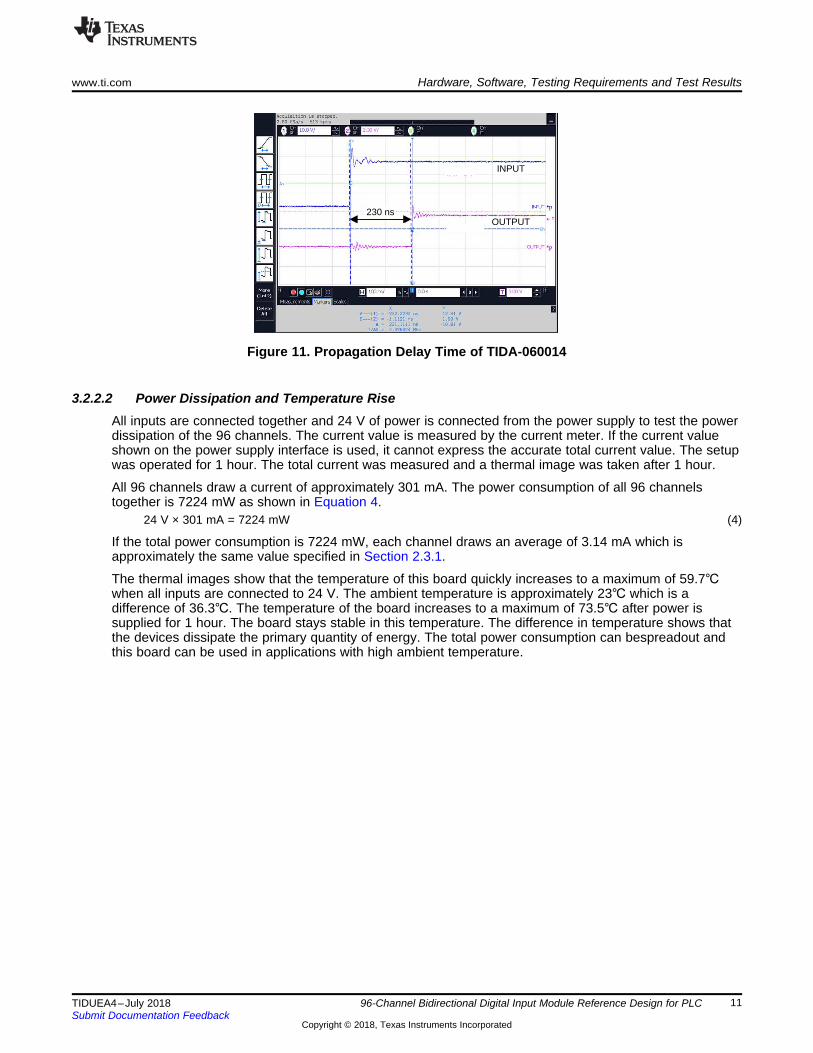
3.2.2.1.2 Propagation Delay TimeOnly one channel can be selected to measure the propagation delay of ISO1212 device. A 24-V squarewaveform with a frequency of 500 kHz (data rate of 1 Mbps) was applied to the field signal connector.Figure 11 shows the propagation delay time as approximately 230 ns. This propagation delay time is alittle greater than the value specified in the ISO1212 data sheet.
96-Channel Bidirectional Digital Input Module Reference Design for PLC
Figure 11. Propagation Delay Time of TIDA-060014
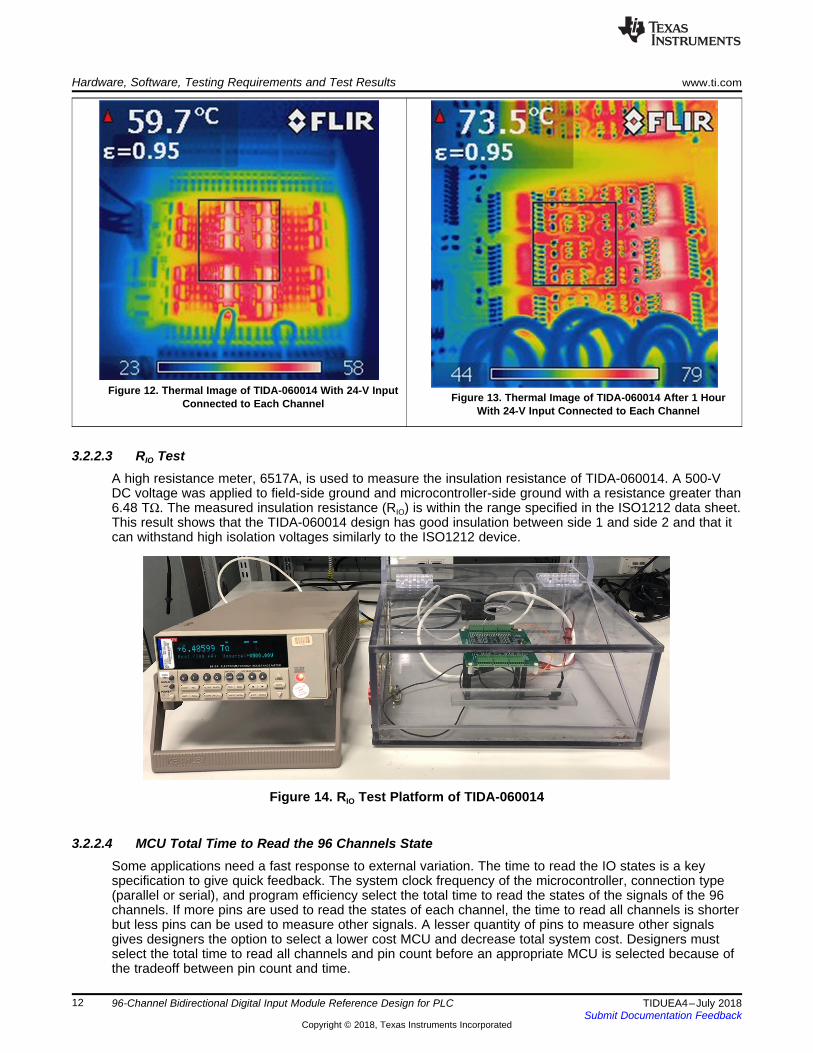
3.2.2.2 Power Dissipation and Temperature RiseAll inputs are connected together and 24 V of power is connected from the power supply to test the powerdissipation of the 96 channels. The current value is measured by the current meter. If the current valueshown on the power supply interface is used, it cannot express the accurate total current value. The setupwas operated for 1 hour. The total current was measured and a thermal image was taken after 1 hour.
All 96 channels draw a current of approximately 301 mA. The power consumption of all 96 channelstogether is 7224 mW as shown in Equation 4.
24 V × 301 mA = 7224 mW (4)
If the total power consumption is 7224 mW, each channel draws an average of 3.14 mA which isapproximately the same value specified in Section 2.3.1.
The thermal images show that the temperature of this board quickly increases to a maximum of 59.7when all inputs are connected to 24 V. The ambient temperature is approximately 23 which is adifference of 36.3. The temperature of the board increases to a maximum of 73.5 after power issupplied for 1 hour. The board stays stable in this temperature. The difference in temperature shows thatthe devices dissipate the primary quantity of energy. The total power consumption can bespreadout andthis board can be used in applications with high ambient temperature.
96-Channel Bidirectional Digital Input Module Reference Design for PLC
Figure 12. Thermal Image of TIDA-060014 With 24-V InputConnected to Each Channel Figure 13. Thermal Image of TIDA-060014 After 1 Hour
With 24-V Input Connected to Each Channel
3.2.2.3 RIO TestA high resistance meter, 6517A, is used to measure the insulation resistance of TIDA-060014. A 500-VDC voltage was applied to field-side ground and microcontroller-side ground with a resistance greater than6.48 TΩ. The measured insulation resistance (RIO) is within the range specified in the ISO1212 data sheet.This result shows that the TIDA-060014 design has good insulation between side 1 and side 2 and that itcan withstand high isolation voltages similarly to the ISO1212 device.
Figure 14. RIO Test Platform of TIDA-060014
3.2.2.4 MCU Total Time to Read the 96 Channels StateSome applications need a fast response to external variation. The time to read the IO states is a keyspecification to give quick feedback. The system clock frequency of the microcontroller, connection type(parallel or serial), and program efficiency select the total time to read the states of the signals of the 96channels. If more pins are used to read the states of each channel, the time to read all channels is shorterbut less pins can be used to measure other signals. A lesser quantity of pins to measure other signalsgives designers the option to select a lower cost MCU and decrease total system cost. Designers mustselect the total time to read all channels and pin count before an appropriate MCU is selected because ofthe tradeoff between pin count and time.
96-Channel Bidirectional Digital Input Module Reference Design for PLC
3.2.2.4.1 Use MSP430F5529 LaunchPad™ Development Kit to Read States of 96 ChannelsThis design uses the multiplexer and decoder to decease the total number of pins connected to themicrocontroller. The MSP430F5529 LaunchPad development kit powers the TIDA-060014 and reads thestates of the input signals of the 96 channels. Table 6 shows the pin configuration and primary code toread the state of each channel signal.
Table 6. Pin Configuration of MSP430F5529
Board Label Signal MSP430F5529 Pin FunctionD1 P2.0 Read state
The term P3 in this code is used to select the group number. The term P6 in this code is used to selectthe channel number. Use the Switch_input_state() function to map the states of the read states and inputsignal states.
3.2.2.4.2 Use MSP430F5529 Timer A to Calculate the Total TimeThis code shows how to use Timer A to calculate the total time to read the states of all channels. Timer Ais used to count the total time. The method to calculate the time is to enable timer A before the code readsthe IO states and to disable the timer after the readout is complete. A breakpoint can be used to read thetimer count number. The total time for a 25-MHz system clock frequency of the MSP430F5529 is 125.2 µsas shown in Equation 5.
96-Channel Bidirectional Digital Input Module Reference Design for PLC
Figure 15. Count Number of TA0R
3.2.2.5 Surge TestThe digital input module must pass tests for surge (caused by lightning strikes), ESD (component contactwith human operators), and EFT (cables near high-voltage and high-frequency signal). The surgewaveform impulse condition for the highest energy and widest pulse width is the hardest condition to passand is therefore most important test to pass.
3.2.2.5.1 Test Set UpThe module needs these surge level 1 tests (500 V, 42 Ω) at the I/O connectors: line-to-PE (earth), line-to-line (differential-mode), and line-to-FGND (common-mode). All input channels must be exposed to a 500-V surge and 1-kV surge out of a 42-Ω generator impedance in accordance with the IEC 61000-4-5standard. Figure 16 shows a wiring diagram example of surge test.
Figure 16. Surge Test Platform Wiring Diagram
The primary surge test steps are:Step 1. Connect the element under test (EUT) as shown in Figure 16.Step 2. Connect the pulse output pin of UTP ED3 to TIDA-060014.Step 3. Wait for five 25-A current peak pulses to be applied in the positive direction.Step 4. Wait for five 25-A current peak pulses to be applied in the negative direction. The time
between two pulses is 10 s. All test channels receive 0.5-kV and 1-kV DM and CM pulses inthis test.
Step 5. Wait for characterization of the board after it is exposed to the surge events. Thischaracterization focuses primarily on the current limit and functional level test.
96-Channel Bidirectional Digital Input Module Reference Design for PLC
The surge test is done with the board powered and unpowered.
3.2.2.5.2 Test ResultsThe surge test was done at a facility of the CSA Group. The equipment (generator, voltage levels, pulseshapes, and generator source impedances) and methods were in accordance with IEC 61131-2 and IEC61000-4-5.
Table 7 shows that the current limit is stable throughout the surge test when the board is unpowered. Thecurrent limit before and after the surge test is almost the same. This similarity shows that the filteringcircuit has a good performance in this design. Use TVS diodes or varistors to meet EMC requirements forsurge tests that need a higher voltage level or faster systems.
Table 7. Board Unpowered Surge Test Results
Test Item Test LevelCurrent Limit Before
Surge Test,Each Channel
Current Limit AfterSurge Test,
Each ChannelTest Result
Common mode (line to FGND)0.5 kV 3.14 mA 3.14 mA Pass1 kV 3.14 mA 3.14 mA Pass
Differential mode (line to line)0.5 kV 3.14 mA 3.14 mA Pass1 kV 3.14 mA 3.14 mA Pass
Table 8 shows the voltage level of each channel to pass the surge test when the board is powered. Thiscircuit can pass a surge voltage that is less than 800 V in the CM surge test. If the surge voltage is greaterthan 800 V, the current limit is greater than 3.1 mA. The circuit broke under these conditions in this test.This circuit can pass a surge voltage that is less than 900 V in the DM surge test.
IN70 to IN69 Pass Pass Pass Pass PassIN68 to IN67 — — Pass Pass Pass
Table 9 shows that a greater value for CIN increases the RC time constant and results in a higher voltagelevel of surge performance. A 1.1-µF capacitor was used in the ISO1212 input stage circuit. The LINE toFGND passes the 1.1-kV surge test. Use TVS diodes or varistors to meet EMC requirements for surgetests that need a higher voltage level or faster systems.
96-Channel Bidirectional Digital Input Module Reference Design for PLC
4 Design Files
4.1 SchematicsTo download the schematics, see the design files at TIDA-060014.
4.2 Bill of MaterialsTo download the bill of materials (BOM), see the design files at TIDA-060014.
4.3 Altium ProjectTo download the Altium Designer® project files, see the design files at TIDA-060014.
4.4 Gerber FilesTo download the Gerber files, see the design files at TIDA-060014.
4.5 Assembly DrawingsTo download the assembly drawings, see the design files at TIDA-060014.
5 Software FilesTo download the software files, see the design files at TIDA-060014.
6 Related DocumentationFor related documentation, see:1. Texas Instruments, ISO121x Isolated 24-V to 60-V Digital Input Receivers for Digital Input Modules2. Texas Instruments, CD74HC238High-Speed CMOS Logic 3- to 8-Line Decoder/Demultiplexer Inverting
and Noninverting3. Texas Instruments, CD74HC4067 High-Speed CMOS Logic 16-Channel Analog
Multiplexer/Demultiplexer
6.1 TrademarksE2E, LaunchPad are trademarks of Texas Instruments.Altium Designer is a registered trademark of Altium LLC or its affiliated companies.All other trademarks are the property of their respective owners.
7 About the AuthorCharles Lin is a field application engineer for the East China team at Texas Instruments. In this role, hesupports industrial customers, writes application notes, and develops reference designs. Charles receivedhis master's degree in electric engineering in 2017 at Xiamen University in China.
Thank you to Anant Kamath and Abhijeeth Aarey for their continuous feedback and support throughoutthe design process.
IMPORTANT NOTICE FOR TI DESIGN INFORMATION AND RESOURCES
Texas Instruments Incorporated (‘TI”) technical, application or other design advice, services or information, including, but not limited to,reference designs and materials relating to evaluation modules, (collectively, “TI Resources”) are intended to assist designers who aredeveloping applications that incorporate TI products; by downloading, accessing or using any particular TI Resource in any way, you(individually or, if you are acting on behalf of a company, your company) agree to use it solely for this purpose and subject to the terms ofthis Notice.TI’s provision of TI Resources does not expand or otherwise alter TI’s applicable published warranties or warranty disclaimers for TIproducts, and no additional obligations or liabilities arise from TI providing such TI Resources. TI reserves the right to make corrections,enhancements, improvements and other changes to its TI Resources.You understand and agree that you remain responsible for using your independent analysis, evaluation and judgment in designing yourapplications and that you have full and exclusive responsibility to assure the safety of your applications and compliance of your applications(and of all TI products used in or for your applications) with all applicable regulations, laws and other applicable requirements. Yourepresent that, with respect to your applications, you have all the necessary expertise to create and implement safeguards that (1)anticipate dangerous consequences of failures, (2) monitor failures and their consequences, and (3) lessen the likelihood of failures thatmight cause harm and take appropriate actions. You agree that prior to using or distributing any applications that include TI products, youwill thoroughly test such applications and the functionality of such TI products as used in such applications. TI has not conducted anytesting other than that specifically described in the published documentation for a particular TI Resource.You are authorized to use, copy and modify any individual TI Resource only in connection with the development of applications that includethe TI product(s) identified in such TI Resource. NO OTHER LICENSE, EXPRESS OR IMPLIED, BY ESTOPPEL OR OTHERWISE TOANY OTHER TI INTELLECTUAL PROPERTY RIGHT, AND NO LICENSE TO ANY TECHNOLOGY OR INTELLECTUAL PROPERTYRIGHT OF TI OR ANY THIRD PARTY IS GRANTED HEREIN, including but not limited to any patent right, copyright, mask work right, orother intellectual property right relating to any combination, machine, or process in which TI products or services are used. Informationregarding or referencing third-party products or services does not constitute a license to use such products or services, or a warranty orendorsement thereof. Use of TI Resources may require a license from a third party under the patents or other intellectual property of thethird party, or a license from TI under the patents or other intellectual property of TI.TI RESOURCES ARE PROVIDED “AS IS” AND WITH ALL FAULTS. TI DISCLAIMS ALL OTHER WARRANTIES ORREPRESENTATIONS, EXPRESS OR IMPLIED, REGARDING TI RESOURCES OR USE THEREOF, INCLUDING BUT NOT LIMITED TOACCURACY OR COMPLETENESS, TITLE, ANY EPIDEMIC FAILURE WARRANTY AND ANY IMPLIED WARRANTIES OFMERCHANTABILITY, FITNESS FOR A PARTICULAR PURPOSE, AND NON-INFRINGEMENT OF ANY THIRD PARTY INTELLECTUALPROPERTY RIGHTS.TI SHALL NOT BE LIABLE FOR AND SHALL NOT DEFEND OR INDEMNIFY YOU AGAINST ANY CLAIM, INCLUDING BUT NOTLIMITED TO ANY INFRINGEMENT CLAIM THAT RELATES TO OR IS BASED ON ANY COMBINATION OF PRODUCTS EVEN IFDESCRIBED IN TI RESOURCES OR OTHERWISE. IN NO EVENT SHALL TI BE LIABLE FOR ANY ACTUAL, DIRECT, SPECIAL,COLLATERAL, INDIRECT, PUNITIVE, INCIDENTAL, CONSEQUENTIAL OR EXEMPLARY DAMAGES IN CONNECTION WITH ORARISING OUT OF TI RESOURCES OR USE THEREOF, AND REGARDLESS OF WHETHER TI HAS BEEN ADVISED OF THEPOSSIBILITY OF SUCH DAMAGES.You agree to fully indemnify TI and its representatives against any damages, costs, losses, and/or liabilities arising out of your non-compliance with the terms and provisions of this Notice.This Notice applies to TI Resources. Additional terms apply to the use and purchase of certain types of materials, TI products and services.These include; without limitation, TI’s standard terms for semiconductor products http://www.ti.com/sc/docs/stdterms.htm), evaluationmodules, and samples (http://www.ti.com/sc/docs/sampterms.htm).