A 0.4 V 75 kbit SRAM Macro in 28 nm CMOSFeaturing a 3-Adjacent MBU Correcting ECC
Adam Neale, Student Member, IEEE, Manoj Sachdev, Fellow, IEEEDepartment of Electrical and Computer Engineering - University of Waterloo
200 University Ave. West, Waterloo, Ontario, Canada, N2L 3G1
Abstract—A 0.4 V single cycle 75 kbit SRAM macro protectedwith a multi-bit upset (MBU) correcting circuit is fabricated ina 28 nm LP-CMOS process. The novel error correcting circuit(ECC) is capable of 3-bit adjacent error correction and 8-bit adjacent error detection. Simulation results show that thecode provides a 2.35x improvement in corrected soft error rate(SER) over a Bose-Chaudhuri-Hocquenghem (BCH) double errorcorrecting (DEC) code at a raw-SER of 1300 FIT/Mb whilerequiring 3 fewer check-bits. Further, an alternative 2-bit adja-cent error correcting implementation provides an corrected-SERapproximately equal to the BCH DEC code for the same check-bit overhead as a single error correcting double error detecting(SEC-DED) code in the same error channel. Measurement resultsconfirm an average active energy of 0.015 fJ/bit and leakagecurrent of 10.1 pA/bit.
I. INTRODUCTION
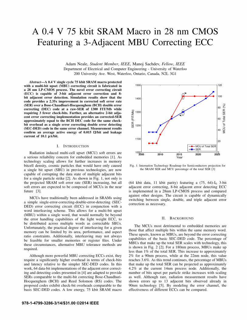
Radiation induced multi-cell upset (MCU) soft errors area serious reliability concern for embedded memories [1]. Astechnology scaling allows for further increases in memorybitcell density, cosmic particles that would have only causeda single bit upset (SBU) in previous technologies, are nowcapable of corrupting the data state of multiple adjacent bitsfor a single particle strike [2]. As shown in Fig. 1, not only isthe projected SRAM soft error rate (SER) increasing, but allsoft errors are expected to be composed of MCUs in the nearfuture [3].
MCUs have traditionally been addressed in SRAMs usinga simple single-error-correcting-double-error-detecting (SEC-DED) error correcting circuit (ECC) in conjunction with aword interleaving scheme. This allows for a multi-bit upset(MBU) within a single word, that would normally be beyondthe error handling capabilities of the light weight ECC, tobe distributed across multiple words as correctable SBUs.Unfortunately, the practical degree of interleaving for a givenmemory can be limited by its area, performance, and aspectratio constraints. Additionally, interleaving may not alwaysbe feasible for smaller memories or register files. Underthese circumstances, alternative MBU tolerance methods arerequired.
Although more powerful MBU correcting ECCs exist, theyrequire a significantly higher overhead in terms of check-bitsand latency relative to the simpler SEC-DED codes. In thiswork, 64 data-bit implementations of the adjacent error correct-ing and detecting codes presented in [4] are adapted to provideSERs comparable to the multi-bit correcting Bose-Chaudhuri-Hocquenghem (BCH) and Reed Solomon (RS) codes. Theproposed codes exhibit check-bit overheads comparable to thebasis SEC-DED codes. A low energy, 75 kbit SRAM macro
2005 2010 2015 2020 20251000
1100
1200
1300
1400
1500
SE
R (
FIT
/Mb)
2005 2010 2015 2020 20250
20
40
60
80
100
120
Year
MC
U o
f T
ota
l S
ER
(%
)
MCU of Total SER
SER
Fig. 1: Internation Technology Roadmap for Semiconductors projection forthe SRAM SER and MCU percentage of the total SER [3]
(64 kbit data, 11 kbit parity) featuring a (75, 64)-I6 3-bitadjacent error correcting, 8-bit adjacent error detecting ECCis implemented in a 28nm LP-CMOS process and comparedagainst other designs. The circuit is capable of dynamicallyswitching between single, double, and triple adjacent errorcorrection as necessary.
II. BACKGROUND
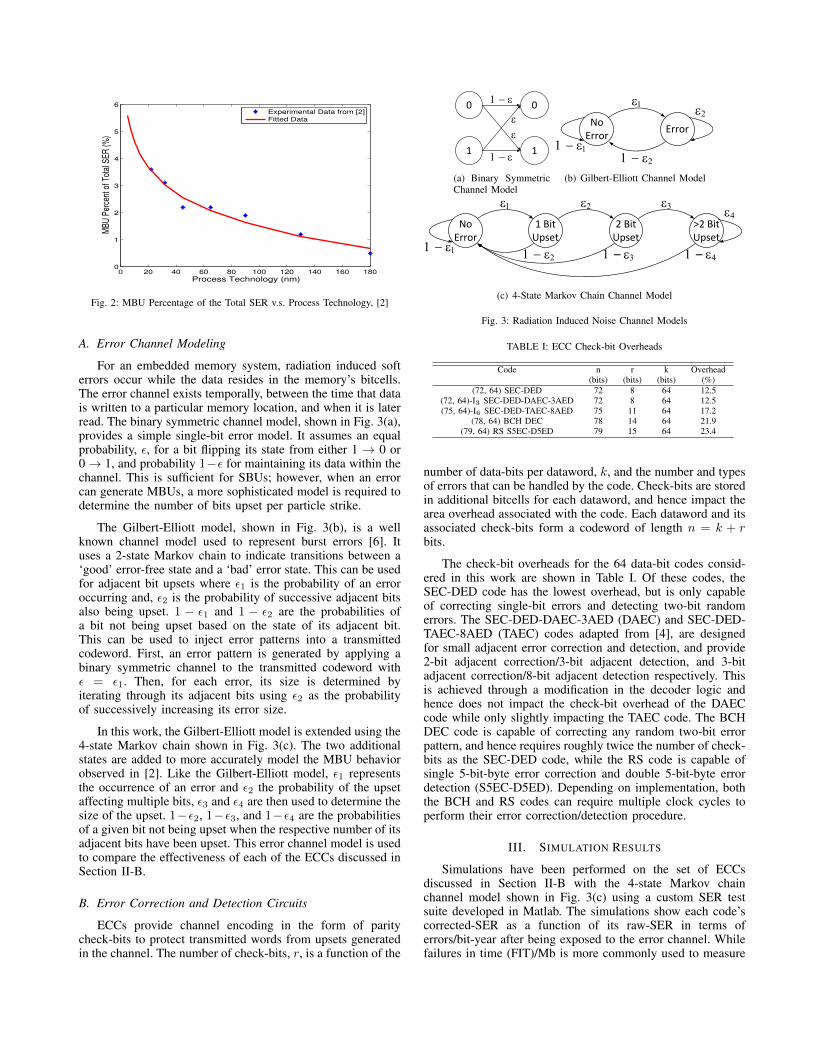
The MCUs most detrimental to embedded memories arethose that affect multiple bits within the same memory word.These upsets, known as MBUs, are beyond the error correctingcapabilities of the basic SEC-DED code. The percentage ofMBUs that make up the total SER scales with technology, thisis shown in Fig. 2 [2]. For a 180nm process, MBUs make upless than 1% of the total SER. This increase to approximately2% for a 90nm process, while at the 22nm node, this valuereaches 3.6%. As this trend continues, the percentage of MBUsthat make up the total SER can be projected as approximately4.2% at the current 14nm process node. Additionally, thenumber of bits upset per particle strike increases with scalingas well. Although rare, radiation measurement results haveshown errors up to 13 adjacent bits observed already in90nm technology [5]. By modeling the error channel, theeffectiveness of different ECCs can be compared.
Fig. 2: MBU Percentage of the Total SER v.s. Process Technology, [2]
A. Error Channel Modeling
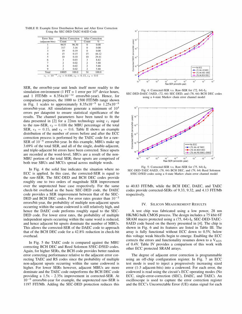
For an embedded memory system, radiation induced softerrors occur while the data resides in the memory’s bitcells.The error channel exists temporally, between the time that datais written to a particular memory location, and when it is laterread. The binary symmetric channel model, shown in Fig. 3(a),provides a simple single-bit error model. It assumes an equalprobability, ε, for a bit flipping its state from either 1 → 0 or0→ 1, and probability 1−ε for maintaining its data within thechannel. This is sufficient for SBUs; however, when an errorcan generate MBUs, a more sophisticated model is required todetermine the number of bits upset per particle strike.
The Gilbert-Elliott model, shown in Fig. 3(b), is a wellknown channel model used to represent burst errors [6]. Ituses a 2-state Markov chain to indicate transitions between a‘good’ error-free state and a ‘bad’ error state. This can be usedfor adjacent bit upsets where ε1 is the probability of an erroroccurring and, ε2 is the probability of successive adjacent bitsalso being upset. 1 − ε1 and 1 − ε2 are the probabilities ofa bit not being upset based on the state of its adjacent bit.This can be used to inject error patterns into a transmittedcodeword. First, an error pattern is generated by applying abinary symmetric channel to the transmitted codeword withε = ε1. Then, for each error, its size is determined byiterating through its adjacent bits using ε2 as the probabilityof successively increasing its error size.
In this work, the Gilbert-Elliott model is extended using the4-state Markov chain shown in Fig. 3(c). The two additionalstates are added to more accurately model the MBU behaviorobserved in [2]. Like the Gilbert-Elliott model, ε1 representsthe occurrence of an error and ε2 the probability of the upsetaffecting multiple bits, ε3 and ε4 are then used to determine thesize of the upset. 1−ε2, 1−ε3, and 1−ε4 are the probabilitiesof a given bit not being upset when the respective number of itsadjacent bits have been upset. This error channel model is usedto compare the effectiveness of each of the ECCs discussed inSection II-B.
B. Error Correction and Detection Circuits
ECCs provide channel encoding in the form of paritycheck-bits to protect transmitted words from upsets generatedin the channel. The number of check-bits, r, is a function of the
number of data-bits per dataword, k, and the number and typesof errors that can be handled by the code. Check-bits are storedin additional bitcells for each dataword, and hence impact thearea overhead associated with the code. Each dataword and itsassociated check-bits form a codeword of length n = k + rbits.
The check-bit overheads for the 64 data-bit codes consid-ered in this work are shown in Table I. Of these codes, theSEC-DED code has the lowest overhead, but is only capableof correcting single-bit errors and detecting two-bit randomerrors. The SEC-DED-DAEC-3AED (DAEC) and SEC-DED-TAEC-8AED (TAEC) codes adapted from [4], are designedfor small adjacent error correction and detection, and provide2-bit adjacent correction/3-bit adjacent detection, and 3-bitadjacent correction/8-bit adjacent detection respectively. Thisis achieved through a modification in the decoder logic andhence does not impact the check-bit overhead of the DAECcode while only slightly impacting the TAEC code. The BCHDEC code is capable of correcting any random two-bit errorpattern, and hence requires roughly twice the number of check-bits as the SEC-DED code, while the RS code is capable ofsingle 5-bit-byte error correction and double 5-bit-byte errordetection (S5EC-D5ED). Depending on implementation, boththe BCH and RS codes can require multiple clock cycles toperform their error correction/detection procedure.
III. SIMULATION RESULTS
Simulations have been performed on the set of ECCsdiscussed in Section II-B with the 4-state Markov chainchannel model shown in Fig. 3(c) using a custom SER testsuite developed in Matlab. The simulations show each code’scorrected-SER as a function of its raw-SER in terms oferrors/bit-year after being exposed to the error channel. Whilefailures in time (FIT)/Mb is more commonly used to measure
TABLE II: Example Error Distribution Before and After Error CorrectionUsing the SEC-DED-TAEC-8AED Code
Error Size Before Correction After Correction(adjacent-bits) Count % Count %
SER, the error/bit-year unit lends itself more readily to thesimulation environment (1 FIT = 1 error per 109 device hours,and 1 FIT/Mb = 8.354x10⁻¹² errors/bit-year). Hence, forcomparison purposes, the 1000 to 1500 FIT/Mb range shownin Fig. 1 scales to approximately 8.35x10⁻⁹ to 1.25x10⁻⁸
errors/bit-year. All simulations generate a minimum of 104
errors per datapoint to ensure statistical significance of theresults. The channel parameters have been tuned to fit thedata presented in [2] for a 22nm technology using ε1 equalto the raw-SER, ε2 = 0.036 the MBU percentage of the totalSER, ε3 = 0.15, and ε4 = 0.6. Table II shows an exampledistribution of the number of errors before and after the ECCcorrection process is performed by the TAEC code for a raw-SER of 10−6 errors/bit-year. In this example, MBUs make up3.69% of the total SER, and all of the single, double-adjacent,and triple-adjacent bit errors have been corrected. Since upsetsare recorded at the word-level, SBUs are a result of the non-MBU portion of the total SER; these upsets are comprised ofboth true SBUs and MCUs spread across multiple words.
In Fig. 4 the solid line indicates the situation where noECC is applied. In this case, the corrected-SER is equal tothe raw-SER. The SEC-DED and BCH DEC codes provideroughly one to two orders of magnitude SER improvementover the unprotected base case respectively. For the samecheck-bit overhead as the basic SEC-DED code, the DAECcode provides a SER improvement between that of the SEC-DED and BCH DEC codes. For error rates greater than 10−3
errors/bit-year, the probability of multiple non-adjacent upsetsoccurring within the same codeword is still relatively high, andhence the DAEC code preforms roughly equal to the SEC-DED code. For lower error rates, the probability of multipleindependent upsets occurring within the same word is reduced,and hence adjacent bit upsets dominate the number of MBUs.This allows the corrected-SER of the DAEC code to approachthat of the BCH DEC code for a 42.8% reduction in check-bitoverhead.
In Fig. 5 the TAEC code is compared against the MBUcorrecting BCH DEC and Reed Solomon S5EC-D5ED codes.Again, for higher SERs, the BCH code provides better randomerror correcting performance relative to the adjacent error cor-recting TAEC and RS codes since the probability of multiplenon-adjacent upsets occurring within the same codeword ishigher. For lower SERs however, adjacent MBUs are moredominate and the TAEC code outperforms the BCH DEC codeproviding a 1.5x - 2.35x improvement in corrected-SER. At10−8 errors/bit-year for example, the unprotected raw-SER is1197 FIT/Mb. Adding the SEC-DED protection reduces this
10−10
10−9
10−8
10−7
10−6
10−5
10−4
10−3
10−2
10−12
10−10
10−8
10−6
10−4
10−2
Raw SER (errors/bit−year)
Co
rre
cte
d S
ER
(e
rro
rs/b
it−
ye
ar)
No ECC
(72, 64)−I3 DAEC
(72, 64) SEC−DED
(78, 64) BCH DEC
Fig. 4: Corrected-SER v.s. Raw-SER for (72, 64)-I3SEC-DED-DAEC-3AED, (72, 64) SEC-DED, and (78, 64) BCH DEC codes
using a 4-state Markov chain error channel model
10−10
10−9
10−8
10−7
10−6
10−5
10−4
10−3
10−2
10−12
10−10
10−8
10−6
10−4
10−2
Raw SER (errors/bit−year)
Co
rre
cte
d S
ER
(e
rro
rs/b
it−
ye
ar)
No ECC
(75, 64)−I6 TAEC
(78, 64) BCH DEC
(79, 64) RS S5EC−D5ED
Fig. 5: Corrected-SER v.s. Raw-SER for (75, 64)-I6SEC-DED-TAEC-8AED, (78, 64) BCH DEC, and (79, 64) Reed Solomon
S5EC-D5ED codes using a 4-state Markov chain error channel model
to 40.83 FIT/Mb, while the BCH DEC, DAEC, and TAECcodes provide corrected-SERs of 9.33, 9.32, and 4.13 FIT/Mbrespectively.
IV. SILICON MEASUREMENT RESULTS
A test chip was fabricated using a low power, 28 nmHK/MG bulk CMOS process. The design includes a 75 kbit 6TSRAM macro protected using a (75, 64)-I6 SEC-DED-TAEC-8AED code based on the theory presented in [4]. The chip isshown in Fig. 6 and its features are listed in Table III. Thearray is fully functional without ECC down to 0.5V, belowthis voltage weak bitcells begin to emerge. Enabling the ECCcorrects the errors and functionality resumes down to a VMIN
of 0.4V. Table IV provides a comparison of this work withother ECC protected SRAM arrays.
The degree of adjacent error correction is programmableusing an off-chip configuration register. In Fig. 7 an ECCtest mode is used to inject a progressively increasing sizederror (1-3 adjacent-bits) into a codeword. For each error, thecodeword is read using the circuit’s ECC operating modes (NoECC, single-error-correction (SEC), DAEC, and TAEC). Anoscilloscope is used to capture the error correction registerand the ECC’s Uncorrectable Error (UE) status signal for each
SRAMSRAM
ECCECC
Fig. 6: 75 kbit SRAM Macro with ECC Die Photo
TABLE III: Features of Fabricated 28nm Test Chip
Process 28nm LP HK+MG Bulk CMOSNominal Supply Voltage 1.0VMemory Capacity 75 kb = 64 kb data + 11 kb parity
256 rows x 300 columns x 1 bankConfiguration 75 bit codeword = 64 data bits + 11 parity bits
4-way interleavingDie: 1.23mm x 1.23mm
Physical Size SRAM: 366.1µm x 146.6µmECC: 139.4µm x 89.3µm
Bitcell Area 1.02µm x 0.379µm = 0.387µm2
(logic design rules)ECC (75, 64)-I6 SEC-DED-TAEC-8AEDECC Features Selectable single, double,
or triple adjacent error correctionMinimum Operating Voltage 0.4V with ECC, 0.5V without ECC
read cycle. As the size of the error increases, more advancedECC modes are required to correct the error. This is detailed inTable V. When the ECC is disabled, none of the injected errorsare correctable. Enabling the basic ECC allows for the single-bit error to be corrected, while enabling the DAEC featureallows for both the single-bit and 2 adjacent bit error to becorrected. Finally, enabling the TAEC feature allows for the 3adjacent bit error to be corrected.
V. CONCLUSION
A 75 kbit SRAM macro protected with an adjacent errorcorrecting and detecting ECC is proposed in this work. Simu-
TABLE IV: Design Comparison
This work JSSC [7] JSSC [8] CICC [9]Year 2014 2006 2009 2013
Leakage (pA/bit) 10.1 91.8 230 353Average Energy (pJ) 1.16 1.55 @ 0.3V 5.34 9.58Average Energy / bit 0.015 0.04 @ 0.3V 0.08 0.018
(fJ/bit)
TABLE V: Measured Error Injection Example
Uncorrectable Error (UE) Correction TypeError Type No ECC SEC DAEC TAEC
Single X 0 0 02-Adjacent X X 0 03-Adjacent X X X 0
0 - Indicates a Correctable Error, X - Indicates an Uncorrectable Error
UE
TAEC
DAEC
SEC
Single bit error 2 adjacent bit error 3 adjacent bit error
SEC
Corrects Error
DAEC
Corrects Error
TAEC
Corrects Error
No
EC
C
SE
C
DA
EC
TA
EC
No
EC
C
SE
C
DA
EC
TA
EC
No
EC
C
SE
C
DA
EC
TA
EC
Fig. 7: Measured error injection example. Additional ECC functionality isrequired to perform error corrections as the injected error size increases.
lation results have shown that for a raw-SER of 1300 FIT/Mb,the DAEC implementation of this code class can providea corrected-SER approximately equal to a BCH DEC codefor the same check-bit overhead as a traditional SEC-DEDcode, and the TAEC implementation provides a 1.5x - 2.35ximprovement in corrected-SER over the BCH DEC for 3 fewercheck-bits. The memory and ECC circuit have been fabricatedin a 28nm LP-CMOS process. Measurement results confirmoperation down to 0.4V with the ECC enabled at a speed of0.92MHz and average energy of 0.015fJ/bit.
ACKNOWLEDGMENT
The authors would like to thank the Canadian Microelec-tronics Corporation for their fabrication support services.
REFERENCES
[1] D. Mavis, P. Eaton, M. Sibley, R. Lacoe, E. J. Smith, and K. Avery,“Multiple Bit Upsets and Error Mitigation in Ultra-Deep SubmicronSRAMs,” Nuclear Science, IEEE Transactions on, vol. 55, no. 6, pp.3288–3294, Dec 2008.
[2] E. Ibe, H. Taniguchi, Y. Yahagi, K.-i. Shimbo, and T. Toba, “Impact ofscaling on neutron-induced soft error in SRAMs from a 250 nm to a 22nm design rule,” Electron Devices, IEEE Transactions on, vol. 57, no. 7,pp. 1527 –1538, July 2010.
[3] International Roadmap for Semiconductors, “http://www.itrs.net/,” 2011.[4] A. Neale and M. Sachdev, “A New SEC-DED Error Correction Code
Subclass for Adjacent MBU Tolerance in Embedded Memory,” Deviceand Materials Reliability, IEEE Transactions on, vol. 13, no. 1, pp. 223–230, March 2013.
[5] R. Naseer and J. Draper, “Parallel double error correcting code design tomitigate multi-bit upsets in SRAM s,” in Solid-State Circuits Conference,2008. ESSCIRC 2008. 34th European, Sept. 2008, pp. 222 –225.
[6] H. Labiod, “Performance of Reed Solomon error-correcting codes onfading channels,” in Personal Wireless Communication, 1999 IEEEInternational Conference on, 1999, pp. 259–263.
[7] T. Suzuki, Y. Yamagami, I. Hatanaka, A. Shibayama, H. Akamatsu,and H. Yamauchi, “A sub-0.5-V operating embedded SRAM featuring amulti-bit-error-immune hidden-ECC scheme,” Solid-State Circuits, IEEEJournal of, vol. 41, no. 1, pp. 152–160, Jan 2006.
[8] S. Jahinuzzaman, J. Shah, D. Rennie, and M. Sachdev, “Design andAnalysis of A 5.3-pJ 64-kb Gated Ground SRAM With Multiword ECC,”Solid-State Circuits, IEEE Journal of, vol. 44, no. 9, pp. 2543–2553, Sept2009.
[9] M. Yabuuchi, H. Fujiwara, Y. Tsukamoto, M. Tanaka, S. Tanaka, andK. Nii, “A 28nm high density 1R/1W 8T-SRAM macro with screeningcircuitry against read disturb failure,” in Custom Integrated CircuitsConference (CICC), 2013 IEEE, Sept 2013, pp. 1–4.