Page 1
1
A 350mK, 9T scanning tunneling microscope for the study of superconducting
thin films on insulating substrates and single crystals
Anand Kamlapure, Garima Saraswat, Somesh Chandra Ganguli, Vivas Bagwe and Pratap Raychaudhuri*
Department of Condensed Matter Physics and Materials Science, Tata Institute of Fundamental
Research, Homi Bhabha Rd., Colaba, Mumbai 400 005, India.
and
Subash P. Pai Excel Instruments, 28, Sarvodaya Industrial Premises, Off Mahakali Caves Road, Andheri
(East), Mumbai 400 093, India.
We report the construction and performance of a low temperature, high field scanning tunneling
microscope (STM) operating down to 350mK and in magnetic fields up to 9T, with thin film
deposition and in-situ single crystal cleaving capabilities. The main focus lies on the simple
design of STM head and a sample holder design that allows us to get spectroscopic data on
superconducting thin films grown in-situ on insulating substrates. Other design details on sample
transport, sample preparation chamber and vibration isolation schemes are also described. We
demonstrate the capability of our instrument through the atomic resolution imaging and
spectroscopy on NbSe2 single crystal and spectroscopic maps obtained on homogeneously
disordered NbN thin film.
* E-mail: [email protected]
Page 2
2
I. Introduction
Ever since its invention, the scanning tunneling microscope (STM)1,2 has emerged as a
powerful spectroscopic tool, combining atomic scale imaging with simultaneous spectroscopic
capabilities. One particularly attractive feature of STS is its unsurpassed energy resolution ( <100
µeV ), limited by thermal broadening of the Fermi edge. This makes the study of unconventional
superconductors using STS particularly attractive since the characteristic energy scales, given by
the superconducting energy gap, ∆, vary from a fraction of a meV to few meV. However, the low
transition temperatures of these superconductors also require the STM to operate at temperatures
well below 1K. Precaution needs to be taken that both tip and sample are at thermal equilibrium
at the same temperature during the measurement.
Over the past few years there are a few3,4,5,6,7,8,9,10,11 STM which can reach temperatures
below 1K incorporating in-situ cleaving and surface cleaning of single crystals and thin film
deposition capabilities. However, a design that allows measurements to be performed on in-situ
grown superconducting films on insulating substrates has remained a challenge. The study of
superconducting thin films on insulating substrates is important for several reasons. First, single
crystalline substrates of insulating MgO, SrTiO3 and LaAlO3 remain the most popular choice for
growing lattice matched high-quality epitaxial thin films of several superconductors used for
basic studies and applications, such as YBa2Cu3O7, (La,Sr)2CuO4 and NbN. More importantly,
the superconducting transition temperature of a superconductor in contact with a normal metal is
suppressed through proximity effect up to a depth of the order of the coherence length, ξ, from
the interface. Since ξ (few nanometers to a few hundred nanometers), is in the same range of the
thickness as most epitaxial films it is important to use insulating substrates in order to study the
intrinsic properties of superconducting films.
Page 3
3
In this paper, we describe the construction of low temperature STM (LT-STM) with base
temperature of 350mK specifically designed for spectroscopic investigations of in-situ
superconducting thin films grown on insulating substrates in a deposition chamber connected to
the STM. In addition, our design also incorporates a crystal cleaving assembly for the study of
superconducting single crystals. The highlights of our STM are a simple stable design of STM
head and a molybdenum sample holder which allows deposition of superconducting thin films on
insulating substrates up to a deposition temperature of 8000C. While most of our measurements
are restricted below 12 K the temperature of the LT-STM can be precisely controlled from 350
mK – 20 K with temperature drift < 10 mK below 3K and < 20 mK in the range 3 - 20 K over 8
hours. We demonstrate topographic imaging with atomic resolution and spectroscopic imaging
down to 350 mK with and without magnetic field.
II. Setup
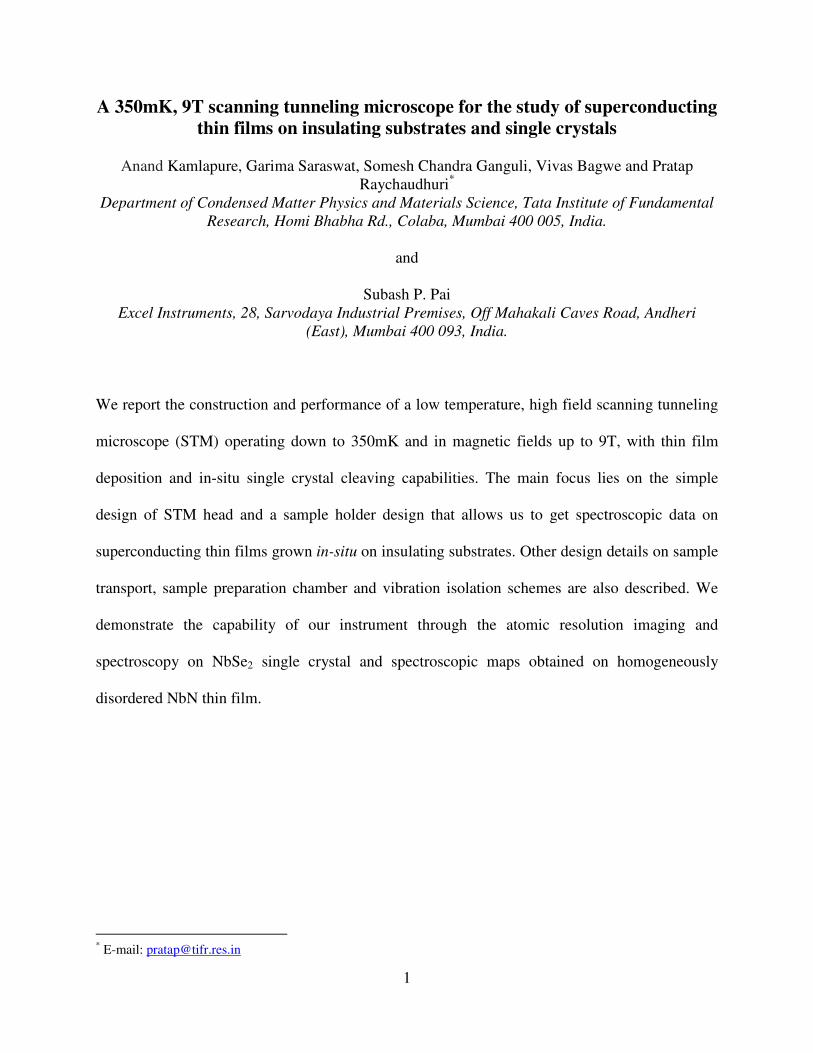
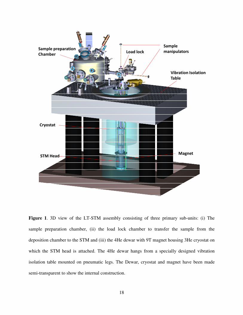
The overall schematic of our system is shown in Fig. 1. The LT-STM assembly consists
of three primary sub-units: (i) The sample preparation chamber, (ii) the load lock chamber to
transfer the sample from the deposition chamber to the STM and (iii) the 4He dewar with 9T
magnet housing 3He cryostat on which the STM head is attached. The 4He dewar hangs from a
specially designed vibration isolation table mounted on pneumatic legs. A combination of active
and passive vibration isolation systems are used to obtain the required mechanical stability of the
tip. Data acquisition is done using the commercial R9 SPM controller from RHK Technology12.
In following subsections we describe the mechanical details of various components of the setup.
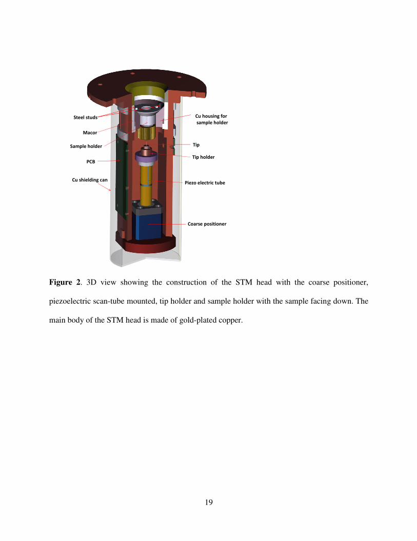
II.A. STM head
Page 4
4
Over the years, several designs of STM heads have been adopted for operation at low
temperatures13,14,15 based on the requirement of stability and convenience of sample or tip
exchange. Some of the popular designs include the Pan type3,16 and Besocke Beetle-type17,18,
which involve coordinated control of multiple piezo elements for coarse positioning. In contrast,
the design of our STM head, which is directly mounted below the 3He pot (Fig. 2) is relatively
simple. In this design both coarse approach as well as scanning is achieved through movement of
the tip whereas the sample is static. The outer body is made of single piece of gold plated oxygen
free high conductivity (OHFC) Copper. The sample holder, coming from the top with the sample
facing down, engages on a Gold plated Copper part which is electrically isolated from the main
body using cylindrical Macor19 machinable ceramic part. Both these parts are glued together
using commercially available low temperature glue20. The copper part has 45° conical cut at the
top matching with sample holder. In the conical region, there are two nonmagnetic stainless steel
studs where sample holder gets locked and it can be disengaged from vertical manipulator. The
copper part also has two leaf springs made of phosphor bronze which grab the sample holder and
also provide better thermal contact and prevent mechanical vibration of the sample holder.
Electrical contact to this copper part is given by soldering a stud which extrude from the lower
side. Positioning unit is located in the cuboidal cavity in the lower part of STM head. One of the
sides of the cavity is open to get access for mounting the positioning unit and changing tip. The
positioning unit consists of a coarse approach positioner and a piezoelectric tube on which the
STM tip is fixed. To bring the tip within tunneling range of the sample we use a coarse
positioner21 which works on the principle of slip-stick motion. The coarse positioner is fixed to a
copper bottom plate using a pair of titanium screws which are in turn screwed to the main body.
Fine positioning and scanning is performed using a 1 inch long piezoelectric tube22 which has
Page 5
5
gold plated electrodes inside and outside. Outside gold plating is divided into two segments. The
lower half is used for Z motion while upper segment has four quadrants and used for XY motion.
Inner electrode is grounded and wrapped out on the upper side to avoid the build-up of any static
charge. The piezo-tube is electrically isolated from coarse positioner at the bottom and the
copper tip carrier on the top through Macor19 pieces which are glued to the tube so as to reduce
differential thermal expansion. The copper tip holder is glued on the upper side of top Macor
piece. We use Pt-Ir wire (80-20%) of diameter 300µm as tip which is held frictionally in 400µm
bore that is drilled on tip holder. Tip is prepared by cutting the Pt-Ir wire using a sharp scissor at
an angle and subsequently field emitted in vacuum at low temperature to achieve the desired
sharpness. Printed circuit boards screwed on the three sides of the cuboid serve as the connecting
stage for electrical connection to the piezo units, sample and tip. Temperature of STM head is
measured using two CernoxTM sensors23 mounted on the bottom plate of the STM as well as on
the 3He pot. The entire STM head is enclosed in gold plated copper can ensuring temperature
homogeneity over the entire length of the head. We observe that after achieving a stable
temperature for about 10 min the temperature of the STM head and 3He pot differ at most by
20mK. The piezo-constants for the scanning head were initially calibrated using lithographically
patterned Au lines of width 100 nm and separation of 100 nm on a metallic substrate, and
subsequently the same calibration was verified through atomic resolution topographic image on
NbSe2.
II. B. Sample holder
The main challenge in the study of superconducting films grown in-situ on insulating
substrates is in establishing the electrical contact with the sample for doing STM experiments.
We overcome this problem by using a design of a sample holder where the film can be directly
Page 6
6
grown in-situ on the insulating substrate fixed on the holder, and subsequently transferred to
STM head for measurement. The sample holder made of molybdenum is shown in Fig. 3. The
choice of the material is given by a trade-off between the need of high thermal conductivity to
ensure temperature homogeneity during measurements and the capacity to withstand temperature
up to 8000C during deposition in reactive atmosphere (e.g. oxygen and nitrogen). The substrate is
mounted with silver epoxy on the top flat surface and fixed in position by fastening a cap having
4.3 mm diameter hole in the center. The edge of the cap makes direct contact with the top surface
of the sample and brings it in electrical contact with the rest of the sample holder. The lower part
of the sample holder ends in a 45° slant which mates with the corresponding part on the STM
head as shown in Fig. 2. The sample holder has a horizontal M4 threads on the side for mounting
on the horizontal manipulator and M6 threads at the bottom for mounting it on the vertical
manipulator. It has two diametrically opposite cuts at the bottom side which fits on the studs on
STM head and locks the circular movement while disengaging the sample holder from the
vertical manipulator after the sample is mounted on the STM head.
For STM measurements on films grown on insulating substrates, first two contact strips
are deposited ex-situ on two edges of the substrate as shown in Fig. 3(b). The width of the strips
is adjusted such that when the substrate with contact pads is mounted on the sample holder, a
small portion of the strip on either side is exposed through the hole in the cap (Fig. 3(d)). When
the superconducting film is deposited on the substrate in the in-situ chamber, the edge of the film
is in contact with the strip and is therefore electrically connected to the entire sample holder. In
principle, the strips could be made of any material that can withstand the deposition temperature
of the superconducting film. However, in most cases we found it convenient to make the strips of
the same material as the material under study. Since our STM head is symmetric, the tip engages
Page 7
7
at the center of the sample which ensures tip to strip distance ~1mm. This is much larger than the
length over which we would expect superconducting proximity effects from the contact pads to
play any role in the measurements.
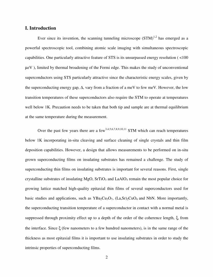
For the study of single crystals a single piece sample holder of similar shape without the
cap is used. The crystal is mounted on the flat surface using a two component conducting silver
epoxy24. Depending on the hardness, the crystal is cleaved in vacuum (in the load lock cross)
alternatively by gluing a small rod on the surface using the same silver epoxy and hitting it with
a hammer or by gluing a tape on the surface and pulling the tape using one of the manipulators.
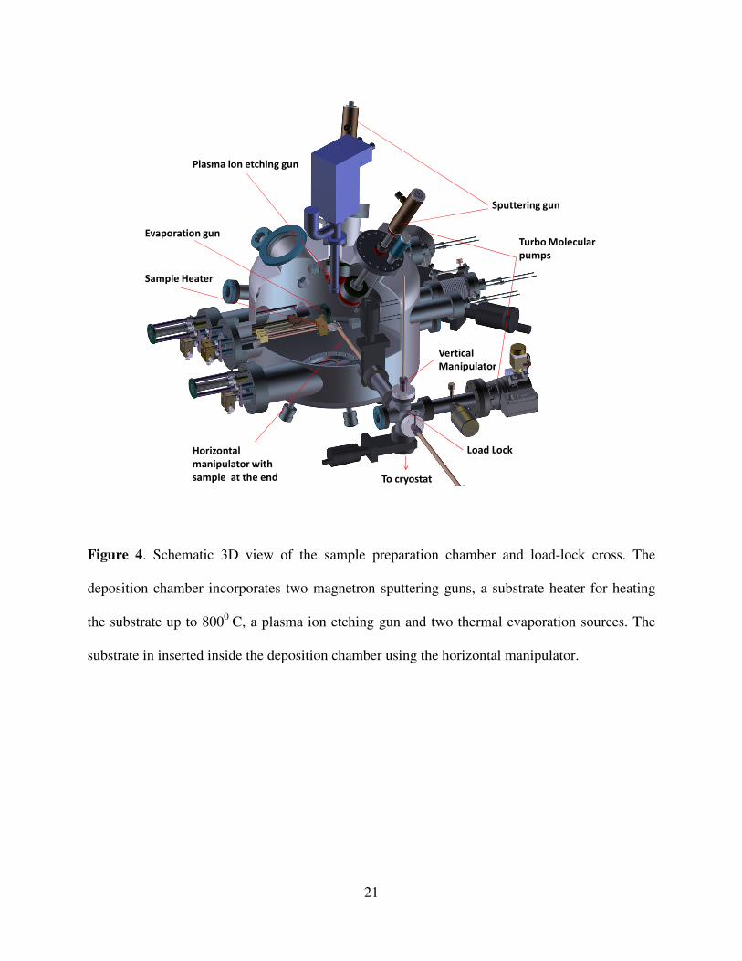
II.C. Sample preparation chamber
The sample preparation chamber, fitted with a turbo molecular pump and with a base
pressure ~ 1×10⁻⁷ mbar, is located on the top of table and is connected to load lock through a gate
valve (Fig 4). The chamber consists of two magnetron sputtering guns facing down at an angle,
to the substrate heater. The confocal arrangement of guns allows for co-sputtering. The substrate
heater consists of a resistive heating element made of a patterned molybdenum plate. Sample
holder is inserted using the horizontal manipulator in the chamber through the load-lock and held
above the heater. It is heated radiatively and its temperature is measured using thermo-couple
(PT100) located inside, at the tip of the horizontal manipulator. In addition, the chamber also
contains a plasma ion source25 for cleaning substrates prior to deposition and two tungsten boats
for thermal evaporation.
II. D. Load lock and sample manipulators
The load-lock, located at the top of the 3He cryostat, has six CF35 ports and it is
connected to sample preparation chamber and STM chamber through gate valves. Typical time
Page 8
8
to pump the load-lock chamber from ambient pressure to 1×10⁻⁶ mbar is about 20 minutes.
Sample manipulators (Fig. 5) are made of seamless steel tubes (closed at one end) and have
matching threads at the end to engage on the corresponding threads on the sample holder. A
thermocouple is fitted inside the horizontal sample manipulator to measure the temperature of
the sample during deposition. Once the sample is deposited horizontal manipulator is pulled back
bringing the sample holder in the cross, and the sample holder is transferred to vertical
manipulator and inserted into the STM head.
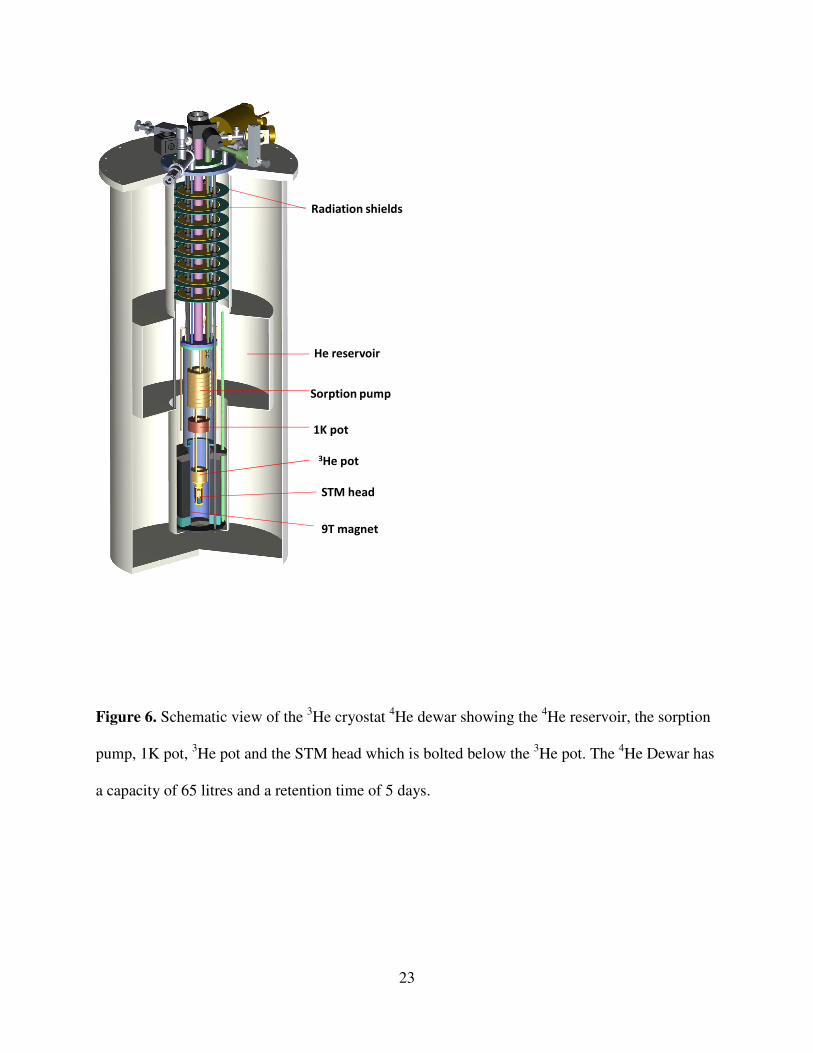
II. E. Cryostat and temperature control of the sample
The low temperature stage consists of an internally fitted charcoal sorption pump based
3He cryostat from Janis Research Company26 (Fig 6). We use a custom design with annular
shaped sorption pump, 1K pot and 3He pot which give us direct line of site access from the top of
the cryostat to the STM head mounted below the 3He pot. To ensure thermal stability the STM
head is bolted to 3He pot using 6 screws which ensures good thermal contact between the two.
To prevent radiative heating, a radiation plug is inserted in the cryostat after loading the sample
using the same vertical manipulator as the one used to insert the sample. The radiation plug (not
shown) sits just above the STM head. The 3He pot and sorption pump are fitted with resistive
heaters. All electrical wires coming from the top are thermally anchored at the 1K pot and the
3He pot. The entire process of cooling the STM from 4.2 K to the base temperature of 350 mK
takes about 20 min with a hold time of about 8 hrs. We wait for about 15 min for after the base
temperature is reached before starting our measurements. Between the base temperature and 3 K,
we control the temperature by controlling the temperature of the sorption pump. For stabilizing
above 3K we use the resistive heater fitted on the 3He pot by keeping the sorption pump
temperature constant at 30 K.
Page 9
9
II.F. Liquid Helium Dewar
The cryostat is mounted in a 65 liters capacity Al-Fibreglass Dewar with retention time of
approximately 5 days. The superconducting magnet with maximum of 9 T aligned along the
STM tip hangs from the top flange of the cryostat. Exhaust line of the cryostat is connected with
one way valve which maintains a constant pressure slightly above atmosphere. This allows us to
flow liquid 4He in a capillary wrapped around the sorption pump such that the sorption pump can
be cooled without using an external pump.
II.G. Vibrational and electrical noise reduction.
Most crucial part of any STM design is the vibrational and electrical noise reduction as it
is directly reflected in the ultimate noise level in the tunneling current. We have adopted three
isolation schemes to reduce vibrational noise. For sound isolation, the entire setup is located in a
sound proof enclosure made of sound proofing perforated foam. To reduce vibrational noise
mainly coming from the building, the entire setup rests on a commercial vibration isolation
table27 (Newport SmartTable®) with integrated active and passive stages with horizontal and
vertical resonant frequency < 1.7 Hz. Finally, since in our cryostat the 1K pot pump has to be on
during STM operation, special precaution has to be taken to isolate the system from the pump
vibrations which get transmitted in two different ways: (i) Direct pump vibration transmitted
through vibration of the connecting bellows and (ii) indirect vibration transmitted through the
sound propagated through the 4He gas in the pumping line. The first source is isolated by
keeping the pumps on a different floor in the basement and a rigid section of the pumping line is
embedded in a heavy concrete block before connecting to the pump. To isolate the second source
of vibration a special pumping scheme is adopted. The 1K pot is connected to the pump through
two alternate pumping lines. While condensing the 3He and cooling the STM head from 4.2K to
Page 10
10
the base temperature, the 1K pot is cooled to 1.6 K by pumping through a 25.4 mm diameter
pumping line directly connected to the pump. Once the base temperature of 350 mK is reached
on the STM head, the first pumping line is closed and the second pumping line is opened. This
line has a 30 cm long 10 cm diameter intermediate section packed with high density polystyrene
foam which isolates the STM from the sound generated by the pump. Since the polystyrene foam
reduces the pumping speed, the 1K pot warms up to 2.8 K, with no noticeable increase in the
temperature of the STM head. During the steady-state operation of the STM at 350 mK the
pumping is further reduced by partially closing a valve to keep the 1K pot at a constant
temperature of ~ 4 K. While operating in this mode we do not observe any difference in vibration
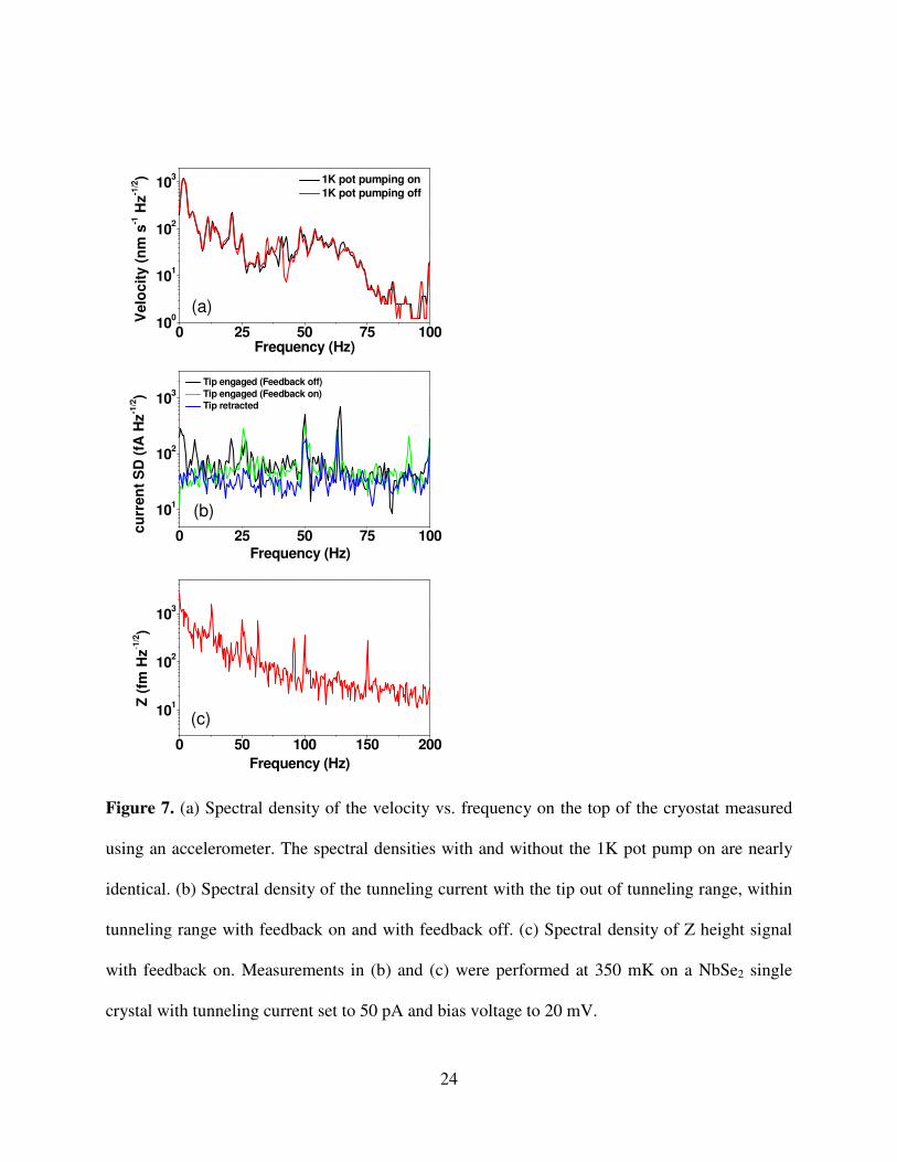
level on the top of the cryostat with the 1K pot pump on or off as shown in Fig. 7(a).
To reduce the electrical noise coming from the 50Hz line signal, ground connection of all
instruments, table and Dewar are made to a separate master ground. RF noise is further reduced
by introducing 10 MHz low pass filter before each connection that goes into the STM. The
tunneling current is detected using a Femto DLPCA-200 current amplifier placed at the top if the
cryostat with gain of 109 V/A. While the bandwidth of the DLCPA-200 amplifier is 500 kHz, the
measurement bandwidth is set digitally restricted to 2.5 kHz in the R9 SPM controller.
The final test of isolation performance is obtained from the spectral density (SD) in the
current and Z-height signals. We recorded these signals at 350 mK in actual operating condition.
Figure 7(b) shows the SD of the current (i) when the tip is out of tunneling range (background
noise of to electronics), (ii) at a fixed tunneling current with feedback on condition, and (iii) after
switching off the feedback for 5 s. The SD with tip out of tunneling range is below 300 fA Hz-1/2.
At fixed tunneling current (feedback on) additional peaks appear in the SD at 25.5 Hz and 91.5
Hz but the peak signal is only marginally larger than 300 fA Hz-1/2. Even after switching off the
Page 11
11
feedback the peak signal is less than 1 pA Hz-1/2. Similarly, the Z-height SD at fixed tunneling
current with feedback on (Fig. 7(c)) is less than 2 pm Hz-1/2 at all frequencies and less than 50 fm
Hz-1/2 above 150 Hz. The low Z-height and current noise allows us to get very good signal to
noise ratio in spectroscopic measurements which we will show in the next section.
III. STM performance
In this section we demonstrate the spatial and energy resolution of our LT-STM through
measurements on Pb single crystal, NbSe2 single crystal and NbN thin films.
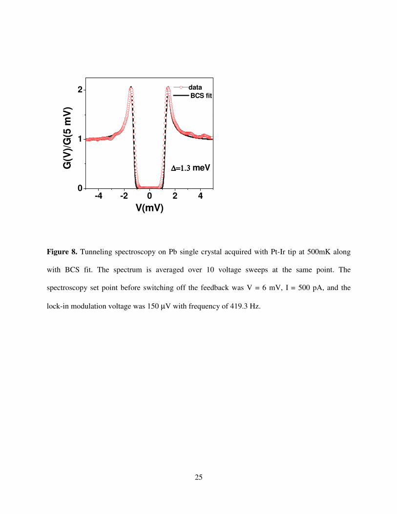
III. A. Tunneling spectroscopy on Pb
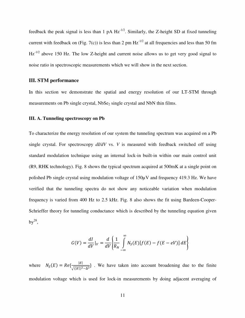
To characterize the energy resolution of our system the tunneling spectrum was acquired on a Pb
single crystal. For spectroscopy dI/dV vs. V is measured with feedback switched off using
standard modulation technique using an internal lock-in built-in within our main control unit
(R9, RHK technology). Fig. 8 shows the typical spectrum acquired at 500mK at a single point on
polished Pb single crystal using modulation voltage of 150µV and frequency 419.3 Hz. We have
verified that the tunneling spectra do not show any noticeable variation when modulation
frequency is varied from 400 Hz to 2.5 kHz. Fig. 8 also shows the fit using Bardeen-Cooper-
Schrieffer theory for tunneling conductance which is described by the tunneling equation given
by28,
���� = ���� | = ��� 1� � ���������� − ��� − �����
�����
where ����� = ��{ |�|��|�|�����} . We have taken into account broadening due to the finite
modulation voltage which is used for lock-in measurements by doing adjacent averaging of
Page 12
12
points in the theoretical curve over a sliding voltage range of 150 µV. BCS fit gives an energy
gap ∆=1.3 meV which is in good agreement29 with reported values of the energy gap in Pb.
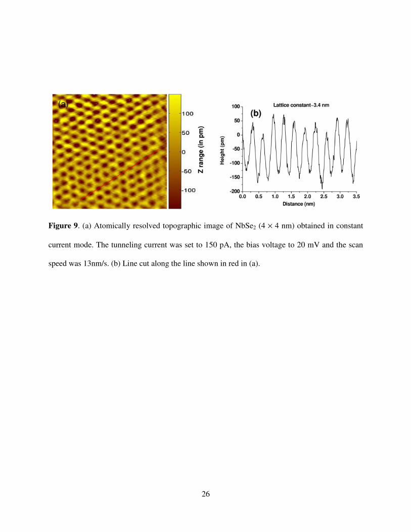
III.B. Atomic resolution and vortex imaging on NbSe2
To test our system for atomic resolution and in magnetic field, we performed
measurements on a 2H-NbSe2 single crystal. Having a hexagonal closed packed layered structure
this crystal can be easily cleaved in-plane. We cleaved the crystal in-situ by attaching a tape on
the surface and subsequently pulling the tape in vacuum in the load-lock chamber using the
sample manipulators. Fig. 9 shows the atomic resolution image at 350mK which reveals the
hexagonal lattice structure. The lattice spacing of 0.34 nm is in very good agreement with the
lattice constant of NbSe2 known from literature.9, 30,31
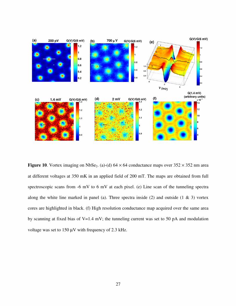
For imaging the vortex state, we have first taken full area spectroscopic map over an area
of 352 × 352 nm in magnetic field of 200mT at 350mK. In this measurement we recorded the
spatially resolved tunneling spectra (dI/dV vs. V) at each point of a grid having 64 × 64 pixels by
sweeping the bias from 6mV to -6mV. Figure 10(a-d) shows intensity plots of the tunneling
conductance normalized at 6mV at different bias voltages, showing the hexagonal vortex lattice.
The lattice constant, a ≈ 109.8 nm is in excellent agreement with the theoretical value expected
from Ginzburg Landau theory28,32. For voltages below ∆/e the vortices appear as regions with
larger conductance whereas for voltages close to the coherence peak the vortices appear as
regions with lower conductance. Fig. 10(e) shows the line scan sectioned on the line shown in
Fig. 10(a). Three representative spectra are highlighted in the figure. Spectra 1 and 3 correspond
to the superconducting region while the spectrum 2 is at the vortex core and has a zero bias
conductance peak which is the signature of Andreev bound state inside the vortex core. In figure
Page 13
13
10(f) we show a high resolution (128 × 128) conductance map obtained by measuring dI/dV at a
fixed bias voltage of 1.4mV while scanning over the same area.
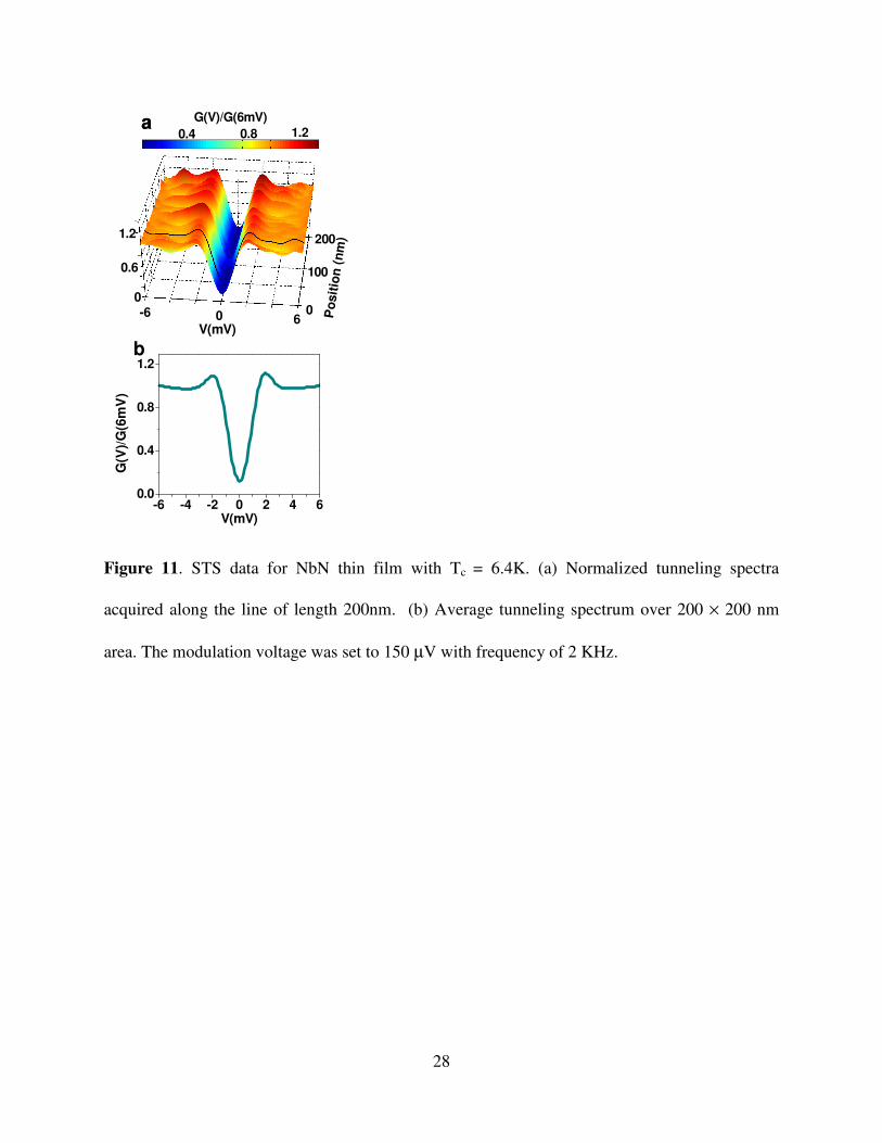
III.C. Scanning tunneling spectroscopy on disordered NbN thin film
As an example of a measurement on thin films we show spatially resolved STS
measurements on a disordered epitaxial NbN thin film grown on single crystalline MgO
substrate. This kind of sample is expected to show variations in the local superconducting order
parameter which in turn reflects in the spatial variation of the coherence peak heights and the
zero bias conductance. The sample was grown in-situ by sputtering Nb in the Ar+N2 mixture
keeping the susbtrate holder33 at 6000C. Tc of the sample measured by four probe technique
(after completing the STS measurements) is 6.4K. For spatially resolved spectroscopy 6
tunneling conductance spectra were acquired at each point on a 32×32 grid over an area of
200×200nm at 500 mK. Figure 11 (a)-(b) show the average of 6 spectra acquired at each point
along a 200 nm line and the average of all the spectra over the entire area. Both individual and
average spectra show the presence of a superconducting gap and coherence peaks at the gap
edge. The coherence peaks are partially suppressed compared to the expectation from BCS
theory which is a hallmark of a strongly disordered superconductor34.
IV. Summary
In summary, we have presented a relatively simple design of a 3He refrigerator based
STM operating down to 350 mK and in magnetic fields up to 9 T. Using a novel design for
sample holder and STM head we demonstrate the capability to perform STM and STS
measurements on in-situ cleaved single crystals and in-situ grown thin films.
Page 14
14
Acknowledgements
We would like to thank Supriya Dhawde for preparing the 3D drawing of the experimental
systems, Parasharam Shirage and A Thamizhavel for providing the NbSe2 single crystals, John
Jesudasan for providing the optimal conditions for deposition of NbN thin films, and Sourin
Mukhopadhyay for being involved in the fabrication of an early 4He version of the STM. The
work was supported by Department of Atomic Energy, Government of India.
Page 15
15
1 G. Binnig, H. Rohrer, Ch. Gerber, and E. Weibel, Phys. Rev. Lett. 50, 120 (1983); Appl. Phys.
Lett. 40, 178 (1982).
2 G. Binnig, H. Rohrer, Surface Sci. 126, 236 (1983).
3 S. H. Pan, E. W. Hudson, and J. C. Davis, Rev. Sci. Instrum. 70, 1459 (1999).
4 Maximilian Assig, Markus Etzkorn, Axel Enders, Wolfgang Stiepany, Christian R. Ast and
Klaus Kern, Rev. Sci. Instrum. 84, 033903 (2013).
5 L. Zhang, T. Miyamachi, T. Tomanić, R. Dehm, and W. Wulfhekel, Rev. Sci. Instrum. 82,
103702 (2011).
6 Young Jae Song, Alexander F. Otte, Vladimir Shvarts, Zuyu Zhao, Young Kuk, Steven R.
Blankenship, Alan Band, Frank M. Hess, and Joseph A. Stroscio, Rev. Sci. Instrum. 81, 121101
(2010).
7 M. Kugler, C. Renner, Ø. Fischer, V. Mikheev, and G. Batey, Rev. Sci. Instrum. 71, 1475
(2000).
8 C. Debuschewitz, F. Münstermann, V. Kunej, and E. Scheer, J. Low Temp. Phys. 147, 525
(2007).
9 H. Kambara, T. Matsui, Y. Niimi, and H. Fukuyama, Rev. Sci. Instrum. 78, 073703 (2007).
10 U. R. Singh, M. Enayat, S. C. White, and P. Wahl, Rev. Sci. Instrum. 84, 013708 (2013).
11 J. Wiebe, A. Wachowiak, F. Meier, D. Haude, T. Foster, M. Morgenstern and R.
Wiesendanger, Rev. Sci. Instrum. 75, 4871 (2004).
12 Control electronics from RHK technology, Inc., USA. Model: R9 SPM Control system.
13 Sang‐il Park and C. F. Quate, Rev. Sci. Instrum. 58, 2010 (1987).
14 Gerhard Meyer, Rev. Sci. Instrum. 67, 2960 (1996).
15 S. J. Ball, G. E. Contant, and A. B. McLean, Rev. Sci. Instrum. 75, 5293 (2004).
Page 16
16
16 Chr. Wittneven, R. Dombrowski, S. H. Pan, and R. Wiesendanger , Rev. Sci. Instrum. 68,
3806 (1997).
17 K. Besocke, Surface Sci. 181, 145 (1987).
18 J. Frohn, J. F. Wolf, K. Besocke, and M. Teske, Rev. Sci. Instrum. 60, 1200 (1989).
19 Machinable ceramic from Corning Glass Corporation
(http://www.corning.com/specialtymaterials/products_capabilites/macor.aspx)
20 Low temperature glue, STYCAST 2850FT, from Emerson and Cuming.
21 Coarse positioner from Attocube Systems AG (model ANPz51).
22 Piezo electric tube from EBL Products, Model EBL#2
23 Cernox sensor from LakeShore Cryotronics Inc., USA.
24 We found the two component silver epoxy EPO-TEK® E4110 from Epoxy Technology, Inc to
have adequate mechanical strength for cleaving most single crystals.
25 Ion source from Tectra GmbH, Frankfurt, Germany. Model: IonEtch sputter Ion Gun, Gen II
26 Janis Research Company, USA. http://www.janis.com/
27 Custom built SmartTable® with central hole from Newport Corporations, USA.
28 Tinkham, M Introduction to Superconductivity (Dover Publications Inc., Mineola, New York,
2004).
29 I. Giaever and K. Megerle, Phys. Rev. 122, 1101 (1961).
30 R. V. Coleman, B. Giambattista, A. Johnson, W. W. McNairy, G. Slough, P. K. Hansma, and
B. Drake, J. Vac. Sci. Technol. A 6, 338 (1988).
31 M. Marz, G. Goll, and H. v. Löhneysen, Rev. Sci. Instrum. 81, 045102 (2010).
32 See supplementary material at [URL will be inserted by AIP] for the variation of vortex lattice constant
as a function of magnetic field.
Page 17
17
33 S. P. Chockalingam, M. Chand, A. Kamlapure, J. Jesudasan, A. Mishra, V. Tripathi, and P.
Raychaudhuri, Phys. Rev. B 77, 214503 (2008).
34 A. Kamlapure, T. Das, S. C. Ganguli, J. B. Parmar, S. Bhattacharyya, and P. Raychaudhuri,
Sci. Rep. 3, 2979 (2013).
Page 18
18
Sample preparation
Chamber
Sample
manipulators
Vibration Isolation
Table
Cryostat
Load lock
STM HeadMagnet
Figure 1. 3D view of the LT-STM assembly consisting of three primary sub-units: (i) The
sample preparation chamber, (ii) the load lock chamber to transfer the sample from the
deposition chamber to the STM and (iii) the 4He dewar with 9T magnet housing 3He cryostat on
which the STM head is attached. The 4He dewar hangs from a specially designed vibration
isolation table mounted on pneumatic legs. The Dewar, cryostat and magnet have been made
semi-transparent to show the internal construction.
Page 19
19
Sample holder Tip
Tip holder
Piezo electric tube
Coarse positioner
Macor
Cu housing for
sample holder
PCB
Cu shielding can
Steel studs
Figure 2. 3D view showing the construction of the STM head with the coarse positioner,
piezoelectric scan-tube mounted, tip holder and sample holder with the sample facing down. The
main body of the STM head is made of gold-plated copper.
Page 20
20
Figure 3. Design of sample holder (a) Molybdenum cap, (b) Substrate with strip deposited at the
edge, (c) Molybdenum sample holder, (d) Sample holder assembly, showing substrate fastened
with cap; (e) Resulting film on the substrate after the deposition.
Page 21
21
Sputtering gun
Plasma ion etching gun
Evaporation gun
Sample Heater
Horizontal
manipulator with
sample at the end
Load Lock
Turbo Molecular
pumps
To cryostat
Vertical
Manipulator
Figure 4. Schematic 3D view of the sample preparation chamber and load-lock cross. The
deposition chamber incorporates two magnetron sputtering guns, a substrate heater for heating
the substrate up to 8000 C, a plasma ion etching gun and two thermal evaporation sources. The
substrate in inserted inside the deposition chamber using the horizontal manipulator.
Page 22
22
Sample holder
To pump
Thermocouple
M4 threading
Wilson seal
CF 35 flange
Figure 5. Design of the horizontal sample manipulator with in-built thermocouple for measuring
the temperature during sample deposition. A differential pumping arrangement between two
Wilson seals is used to remove any leaked gas during movement. The end of the manipulator is
made transparent to show the position of the thermocouple. The vertical manipulator is similar in
construction but does not have the thermocouple.
Page 23
23
Radiation shields
He reservoir
Sorption pump
1K pot
3He pot
STM head
9T magnet
Figure 6. Schematic view of the 3He cryostat 4He dewar showing the 4He reservoir, the sorption
pump, 1K pot, 3He pot and the STM head which is bolted below the 3He pot. The 4He Dewar has
a capacity of 65 litres and a retention time of 5 days.
Page 24
24
0 25 50 75 10010
0
101
102
103
0 25 50 75 100
101
102
103
0 50 100 150 200
101
102
103
Velo
cit
y (
nm
s-1 H
z-1
/2)
Frequency (Hz)
1K pot pumping on
1K pot pumping off
(a)
cu
rren
t S
D (
fA H
z-1
/2)
Frequency (Hz)
Tip engaged (Feedback off)
Tip engaged (Feedback on)
Tip retracted
(b)
Z (
fm H
z-1
/2)
Frequency (Hz)
(c)
Figure 7. (a) Spectral density of the velocity vs. frequency on the top of the cryostat measured
using an accelerometer. The spectral densities with and without the 1K pot pump on are nearly
identical. (b) Spectral density of the tunneling current with the tip out of tunneling range, within
tunneling range with feedback on and with feedback off. (c) Spectral density of Z height signal
with feedback on. Measurements in (b) and (c) were performed at 350 mK on a NbSe2 single
crystal with tunneling current set to 50 pA and bias voltage to 20 mV.
Page 25
25
-4 -2 0 2 40
1
2
G
(V)/
G(5
mV
)
V(mV)
data
BCS fit
∆=1.3∆=1.3∆=1.3∆=1.3 meV
Figure 8. Tunneling spectroscopy on Pb single crystal acquired with Pt-Ir tip at 500mK along
with BCS fit. The spectrum is averaged over 10 voltage sweeps at the same point. The
spectroscopy set point before switching off the feedback was V = 6 mV, I = 500 pA, and the
lock-in modulation voltage was 150 µV with frequency of 419.3 Hz.
Page 26
26
Figure 9. (a) Atomically resolved topographic image of NbSe2 (4 × 4 nm) obtained in constant
current mode. The tunneling current was set to 150 pA, the bias voltage to 20 mV and the scan
speed was 13nm/s. (b) Line cut along the line shown in red in (a).
Page 27
27
Figure 10. Vortex imaging on NbSe2. (a)-(d) 64 × 64 conductance maps over 352 × 352 nm area
at different voltages at 350 mK in an applied field of 200 mT. The maps are obtained from full
spectroscopic scans from -6 mV to 6 mV at each pixel. (e) Line scan of the tunneling spectra
along the white line marked in panel (a). Three spectra inside (2) and outside (1 & 3) vortex
cores are highlighted in black. (f) High resolution conductance map acquired over the same area
by scanning at fixed bias of V=1.4 mV; the tunneling current was set to 50 pA and modulation
voltage was set to 150 µV with frequency of 2.3 kHz.
Page 28
28
-6 -4 -2 0 2 4 60.0
0.4
0.8
1.2b
a
V(mV)
G(V
)/G
(6m
V)
V(mV)
Po
sit
ion
(n
m)200
100
0
1.2
0.6
0-6 0 6
0.4 0.8 1.2
G(V)/G(6mV)a
Figure 11. STS data for NbN thin film with Tc = 6.4K. (a) Normalized tunneling spectra
acquired along the line of length 200nm. (b) Average tunneling spectrum over 200 × 200 nm
area. The modulation voltage was set to 150 µV with frequency of 2 KHz.
Page 29
29
A 350mK, 9T scanning tunneling microscope for the study of superconducting
thin films and single crystals
Anand Kamlapure, Garima Saraswat, Somesh Chandra Ganguli, Vivas Bagwe and Pratap Raychaudhuri*
Department of Condensed Matter Physics and Materials Science, Tata Institute of Fundamental
Research, Homi Bhabha Rd., Colaba, Mumbai 400 005, India.
and
Subash P. Pai
Excel Instruments, 28, Sarvodaya Industrial Premises, Off Mahakali Caves Road, Andheri
(East), Mumbai 400 093, India.
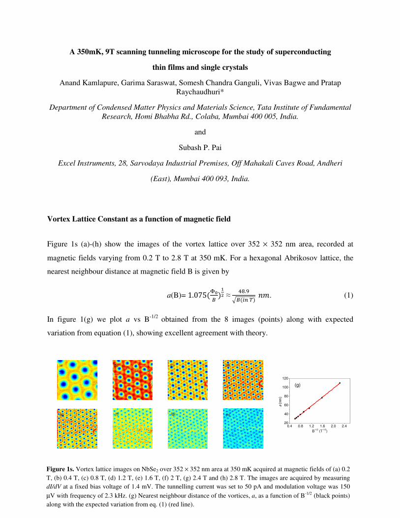
Vortex Lattice Constant as a function of magnetic field
Figure 1s (a)-(h) show the images of the vortex lattice over 352 × 352 nm area, recorded at
magnetic fields varying from 0.2 T to 2.8 T at 350 mK. For a hexagonal Abrikosov lattice, the
nearest neighbour distance at magnetic field B is given by
a(B)= 1.075�%&' �(� ≈ *+.,�'�-./� 01. (1)
In figure 1(g) we plot a vs B-1/2 obtained from the 8 images (points) along with expected
variation from equation (1), showing excellent agreement with theory.
(a)(a)(a)(b)
(e) (f)
(c) (d)
(g) (h)
0.4 0.8 1.2 1.6 2.0 2.420
40
60
80
100
120
a (nm)
B-1/2
(T-1/2
)
(g)
Figure 1s. Vortex lattice images on NbSe2 over 352 × 352 nm area at 350 mK acquired at magnetic fields of (a) 0.2
T, (b) 0.4 T, (c) 0.8 T, (d) 1.2 T, (e) 1.6 T, (f) 2 T, (g) 2.4 T and (h) 2.8 T. The images are acquired by measuring
dI/dV at a fixed bias voltage of 1.4 mV. The tunnelling current was set to 50 pA and modulation voltage was 150
µV with frequency of 2.3 kHz. (g) Nearest neighbour distance of the vortices, a, as a function of B-1/2 (black points)
along with the expected variation from eq. (1) (red line).