A 45nm Logic Technology with High-k + Metal Gate Transistors, Strained Silicon, 9 Cu Interconnect Layers, 193nm Dry Patterning, and 100% Pb-free Packaging K. Mistry , C. Allen, C. Auth, B. Beattie, D. Bergstrom, M. Bost, M. Brazier, M. Buehler, A. Cappellani, R. Chau * , C.-H. Choi, G. Ding, K. Fischer, T. Ghani, R. Grover, W. Han, D. Hanken, M. Hattendorf, J. He # , J. Hicks # , R. Heussner, D. Ingerly, P. Jain, R. James, L. Jong, S. Joshi, C. Kenyon, K. Kuhn, K. Lee, H. Liu, J. Maiz # , B. McIntyre, P. Moon, J. Neirynck, S. Pae # , C. Parker, D. Parsons, C. Prasad # , L. Pipes, M. Prince, P. Ranade, T. Reynolds, J. Sandford, L. Shifren % , J. Sebastian, J. Seiple, D. Simon, S. Sivakumar, P. Smith, C. Thomas, T. Troeger, P. Vandervoorn, S. Williams, K. Zawadzki Portland Technology Development, * CR, # QRE, % PTM Intel Corporation
Transcript
A 45nm Logic Technology with High-k + Metal Gate Transistors, Strained Silicon, 9 Cu
Interconnect Layers, 193nm Dry Patterning, and 100% Pb-free Packaging
K. Mistry, C. Allen, C. Auth, B. Beattie, D. Bergstrom, M. Bost, M. Brazier, M. Buehler, A. Cappellani, R. Chau*, C.-H. Choi, G. Ding, K. Fischer, T. Ghani, R. Grover, W. Han, D. Hanken, M. Hattendorf, J. He#, J. Hicks#, R. Heussner, D. Ingerly, P. Jain, R. James, L. Jong, S. Joshi, C. Kenyon, K. Kuhn, K. Lee,
H. Liu, J. Maiz#, B. McIntyre, P. Moon, J. Neirynck, S. Pae#, C. Parker, D. Parsons, C. Prasad#, L. Pipes, M. Prince, P. Ranade, T. Reynolds,
J. Sandford, L. Shifren%, J. Sebastian, J. Seiple, D. Simon, S. Sivakumar, P. Smith, C. Thomas, T. Troeger, P. Vandervoorn, S. Williams, K. Zawadzki
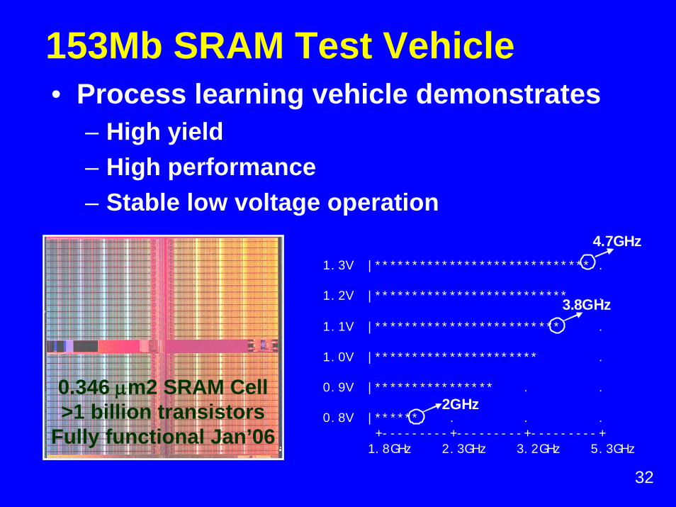
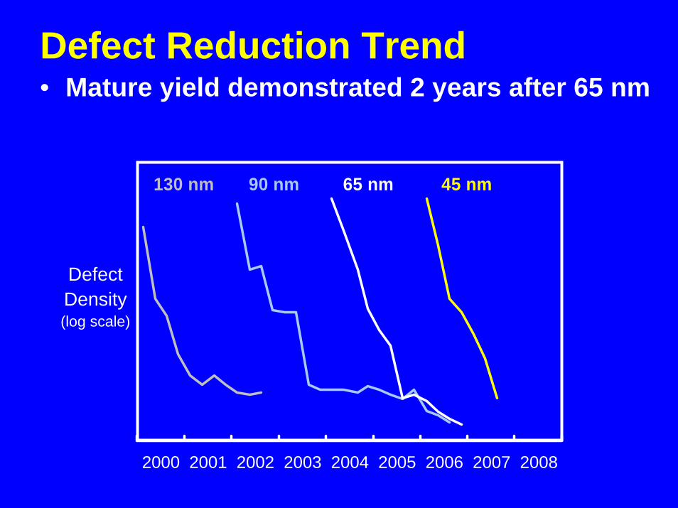
Defect Reduction Trend• Mature yield demonstrated 2 years after 65 nm
Defect Density (log scale)
2000 2001 2002 2003 2004 2005 2006 2007 2008
130 nm 90 nm 65 nm 45 nm
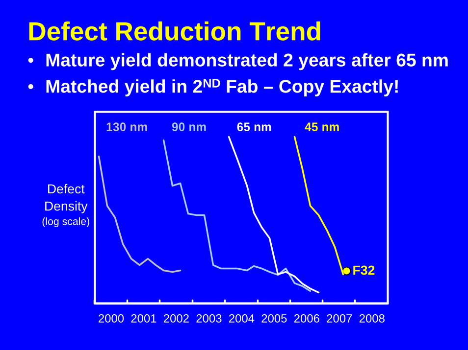
Defect Reduction Trend• Mature yield demonstrated 2 years after 65 nm• Matched yield in 2ND Fab – Copy Exactly!
Defect Density (log scale)
2000 2001 2002 2003 2004 2005 2006 2007 2008
F32
130 nm 90 nm 65 nm 45 nm
35
Conclusions• A 45 nm technology is described with
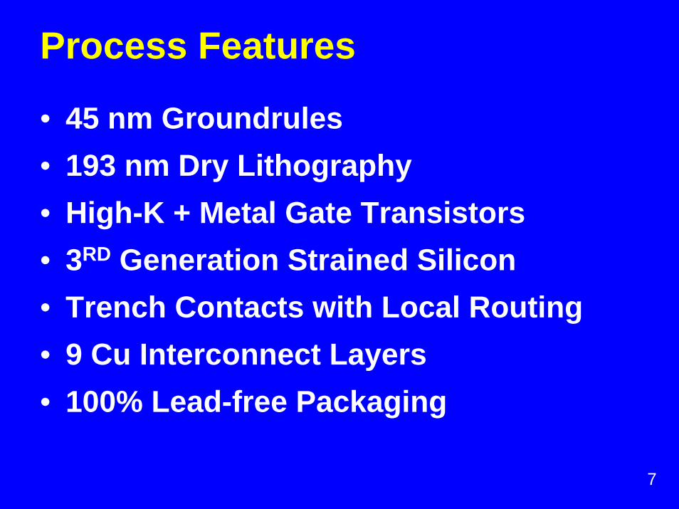
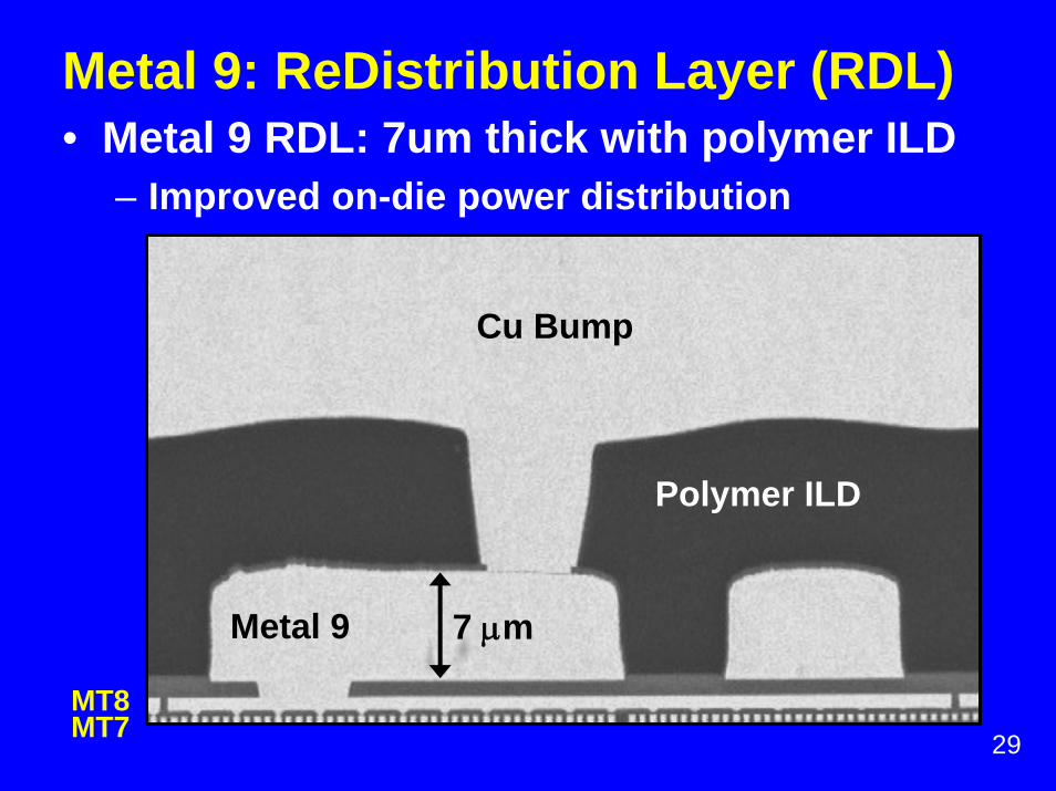
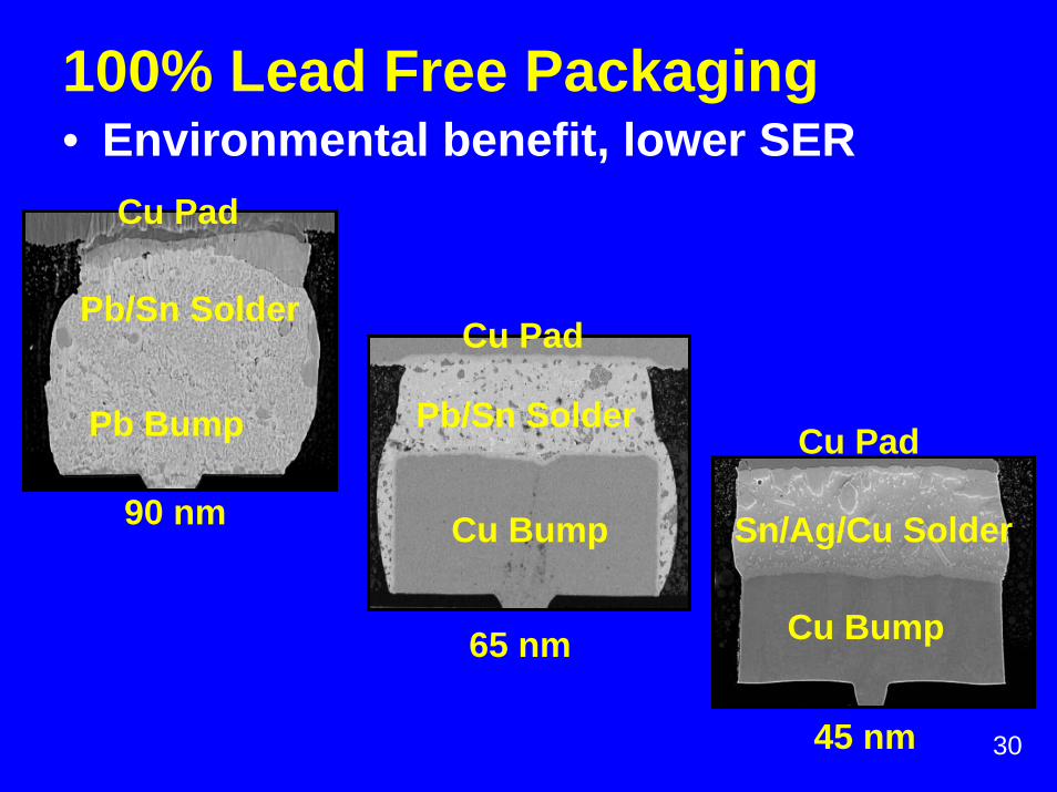
– Design rules supporting ~2X improvement in transistor density– 193nm dry lithography at critical layers for low cost– Trench contacts supporting local routing– 8 standard Cu interconnect layers with extensive use of low-k– Thick Metal 9 Cu RDL with polymer ILD
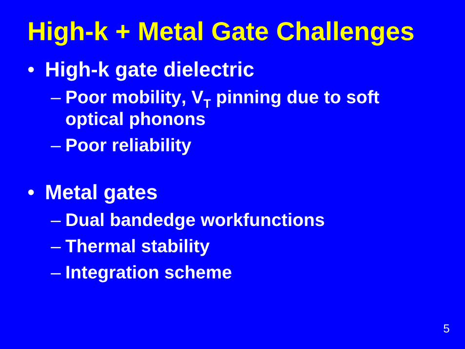
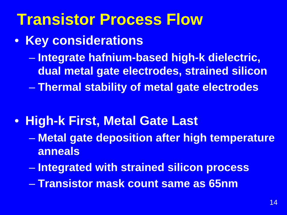
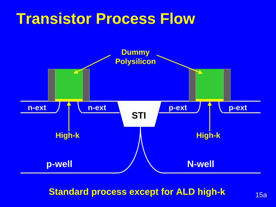
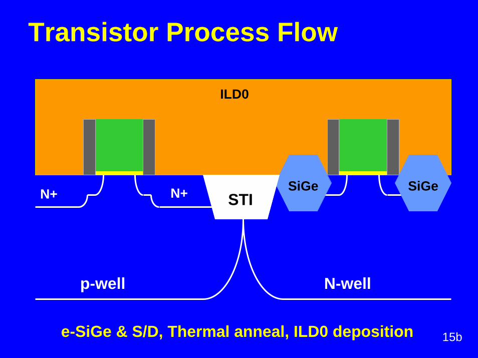
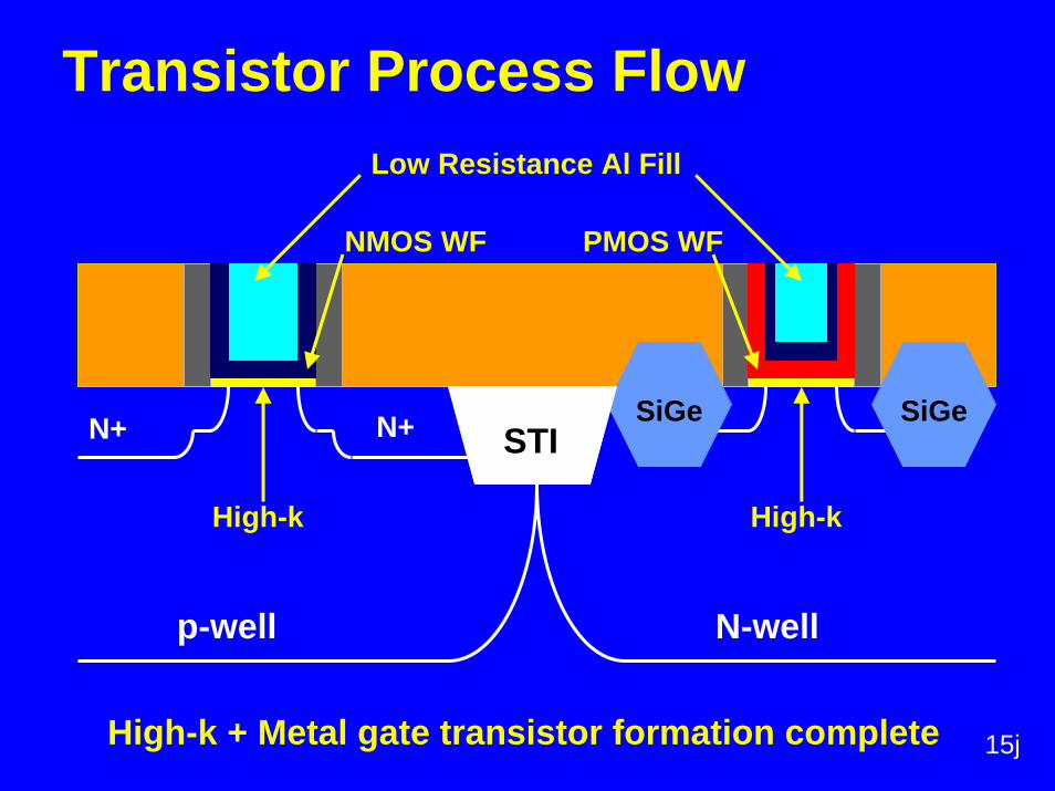
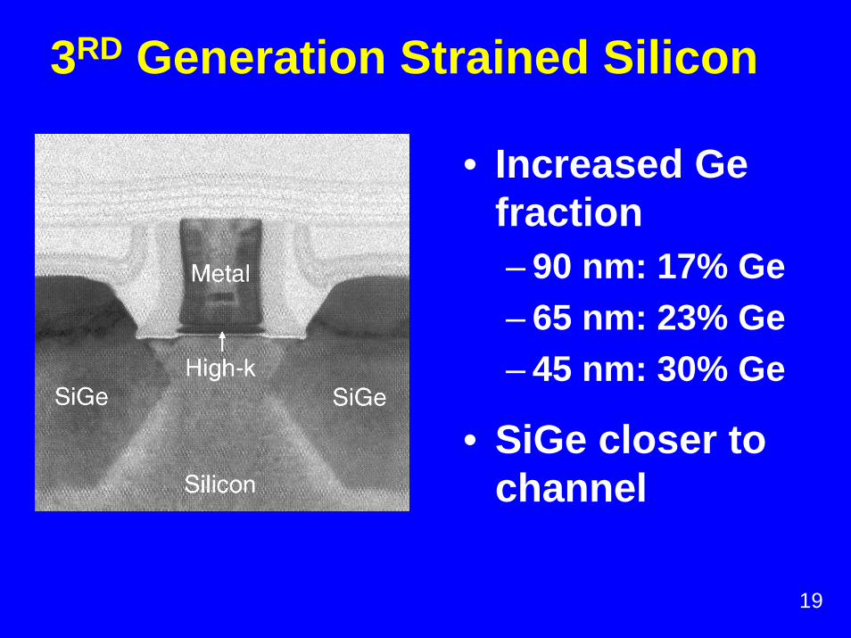
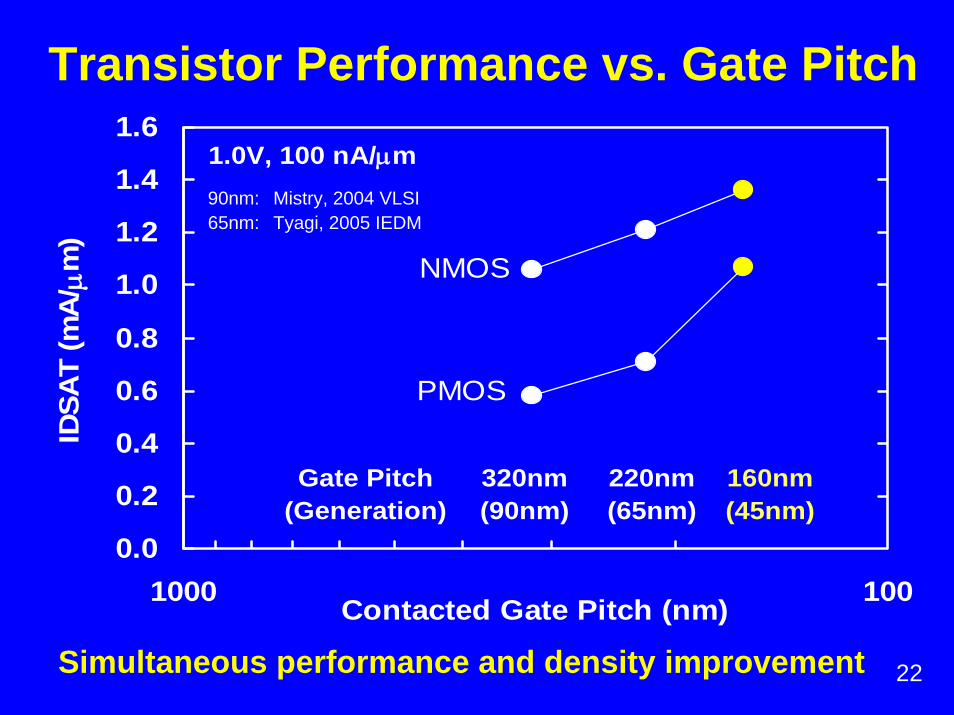
• High-k + Metal gate transistors implemented for the first time in a high volume manufacturing process– Integrated with 3RD generation strained silicon– Achieve record drive currents at low IOFF and tight gate pitch
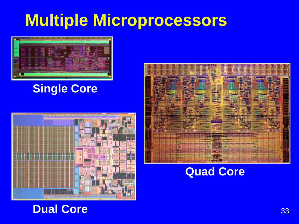
• The technology is already in high volume manufacturing– High yields demonstrated on SRAM and 3 microprocessors– High yields demonstrated in two 300mm fabs
36
Acknowledgements
• The authors gratefully acknowledge the many people in the following organizations at Intel who contributed to this work:– Portland Technology Development – Quality and Reliability Engineering– Process & Technology Modeling– Assembly & Test Technology Development
37
For further information on Intel's silicon technology, please visit our Technology & Research page at


![LOGIC SENSOR PROOUT Gate Driver Providing Galvanic ... · LOGIC SENSOR PROOUT Gate Driver Providing Galvanic ... ... 4]]]](https://static.documents.pub/doc/80x56/5f97e95f3e31877b342a40b6/logic-sensor-proout-gate-driver-providing-galvanic-logic-sensor-proout-gate.jpg)


