2
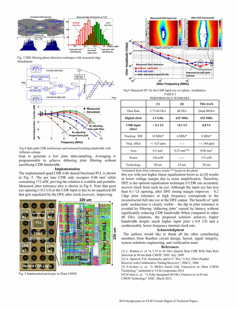
A 4x40 Gb/s Quad-Lane CDR with Shared Frequency Tracking and Data Dependent Jitter Filtering Masum Hossain 1,2 , E-Hung Chen 1 , Reza Navid 1 , Brian Leibowitz 1 , Adam Chou 1 , Simon Li 1 , M J Park 1 , Jihong Ren 1 , Barry Daly 1 , Bruce Su 1 , Makarand Shirasgaonkar 1 , Fred Heaton 1 , Jared Zerbe 1 , John Eble 1 1 Rambus Inc, Sunnyvale, CA 94089 2 University of Alberta, Edmonton, Canada [email protected],[email protected] Abstract A 4x40 Gb/s collaborative digital CDR is implemented in 28nm CMOS. The CDR is capable of recovering a low jitter clock from a partially-equalized or un-equalized eye by using a phase detection scheme that inherently filters out ISI edges. The CDR uses split feedback that simultaneously allows wider bandwidth and lower recovered clock jitter. A shared frequency tracking is also introduced that results in lower periodic jitter. Combining these techniques the CDR recovers a 10GHz clock from an eye containing 0.8UIpp DDJ and still achieves 1-10 MHz of tracking bandwidth while adding < 300fs of jitter. Per lane CDR occupies only .06 mm 2 and consumes 175 mW. Introduction Digital CDRs are area efficient and portable and often preferred over analog solutions for multi-channel SerDes systems. Most of their advantages result from replacing analog charge pumps/loop filters with a synthesizable digital state machine. In most cases the state machine is clocked at a rate significantly slower than the data rate, with this rate scaling conservatively with technology. For example, in 28nm CMOS process, synthesizable logic can operate up to 700MHz over PVT. For 40 Gb/s, this translates to a deserialization ratio of 64. Such a slow phase update rate causes several challenges in CDR design. Because of the slow phase update rate, frequency offset tracking requires larger phase step sizes, thereby increasing jitter. In addition, each digital clock cycle in the state machine translates to 64 UI of latency in the CDR feedback path causing ‘jitter peaking’ [1]. To avoid this phenomena, loop gain must be reduced with the resultant impact on lower CDR bandwidth. Although digital CDRs are desirable for scalable SerDes solutions, significant innovation is required at high-speed, especially with channels that cause significant ISI. CDR Architecture The receiver clocking architectures includes a LC PLL shared across four lanes and per lane DLL and phase mixer with quarter rate CDR. The choice of quarter rate relaxes clock distribution to 10GHz, and the per-lane phase splitting DLL requires only a single phase of the 10 GHz clock to be distributed. This clocking architecture facilitates link scaling with minimal impact on power and performance. A. Shared Frequency tracking SerDes Tx/Rx pairs must often use plesiochronous crystal references with minor frequency offsets. CDRs compensate this frequency offset by continuously rotating the phase interpolator (PI). Since in this quad-configuration the frequency offset is common for all four lanes, the more efficient approach was to use a common PI. Notice that unlike [2], the shared phase rotator is inside the PLLs feedback path in order to filter quantization noise via the PLL’s low pass transfer characteristics. In addition, the Δ-∑ modulator makes the noise filtering more effective via noise shaping. These modifications effectively transform the integer PLL to a fractional PLL with the VCO frequency realigned to the transmitted data. Although test-silicon visibility was limited to a divided version of the recovered clock, frequency spurs generated from continuous phase rotation while tracking a 100ppm frequency offset are clearly shown in Fig. 2. This technique R C up dn PFD % 2 f REF ∆ - ∑ Mod. I Q %N/2 Acc. DDJ Filter PD K P K I D DLL Data K s Shared PLL with freq. tracking Rx CDR #1 Rx CDR #2 Rx CDR #3 Rx CDR #4 20 GHz LC VCO Fig.1 CDR architecture with shared frequency tracking - 40 dB - 40 dB - 56 dB - 57 dB - 40 dB - 53 dB - 65 dB - 53 dB Conventional 2 nd order CDR Using Phase mixer 2 nd order CDR Using Fractional N Fig.2 Measured recovered clock spectrum tracking 100 ppm frequency offset resulted in a lower frequency spur and larger ppm tracking capability without stressing local phase accumulators. B. DDJ filtering phase detector Due to the high data rate, direct feedback DFE is not realizable; therefore, the 1 st post-cursor taps are implemented with loop unrolling . As a result, edge samplers do not see the benefit of time interleaved DFE [3] and the timing loop is required to recover the clock from an eye with 10+ dB of un-equalized ISI. With such large DDJ (0.8UIpp), recovering an optimal data sampling phase is not guaranteed and significant static phase offset is possible. To overcome these issues we propose a phase detection technique that inherently filters out edges with ISI by using positive and negative thresholds (+α and –α) in data samplers to select the zero crossings from reduced ISI patterns. Therefore, the edge distribution seen by the CDR improves and static error is corrected (Fig. 3). C. Split feedback CDR Timing margin of the link is limited by the jitter on the recovered ‘data sampling’ clock. On the other hand, the purpose of the ‘edge sampling’ clock is to track timing error; therefore, jitter on this clock has less impact on timing margin. The proposed split path architecture takes advantage of this observation by splitting the phase error in two paths. Since PD and DFE are driven by separate PI, their phase codes can be filtered differently as shown in Fig.4. PD PI phase code is updated with minimal feedback latency to achieve highest bandwidth. Although the PD clock can then have high jitter, a ‘smoothing filter’ is added outside the phase tracking 978-1-4799-3328-0/14/$31.00 ©2014 IEEE 2014 Symposium on VLSI Circuits Digest of Technical Papers