+ All Categories
Home > Documents > A 5 GHz Voltage Controlled Oscillator (VCO) with 360° variable phase outputs Presented by Tjaart...

A 5 GHz Voltage Controlled Oscillator (VCO) with 360° variable phase outputs Presented by Tjaart...

Date post: 23-Dec-2015
Category:
Upload: alfred-small
View: 225 times
Download: 2 times
Share this document with a friend
Popular Tags:
23
A 5 GHz Voltage Controlled Oscillator (VCO) with 360° variable phase outputs Presented by Tjaart Opperman ( [email protected]) Program: (MEng) Micro-Electronic Engineering (University of Pretoria) Supervisor: Saurabh Sinha
Transcript

A 5 GHz Voltage Controlled Oscillator (VCO) with 360° variable phase outputs

Presented by Tjaart Opperman ( [email protected])

Program: (MEng) Micro-Electronic Engineering (University of Pretoria)

Supervisor: Saurabh Sinha

Slide 2 © CSIR 2006 www.csir.co.za

AGENDA

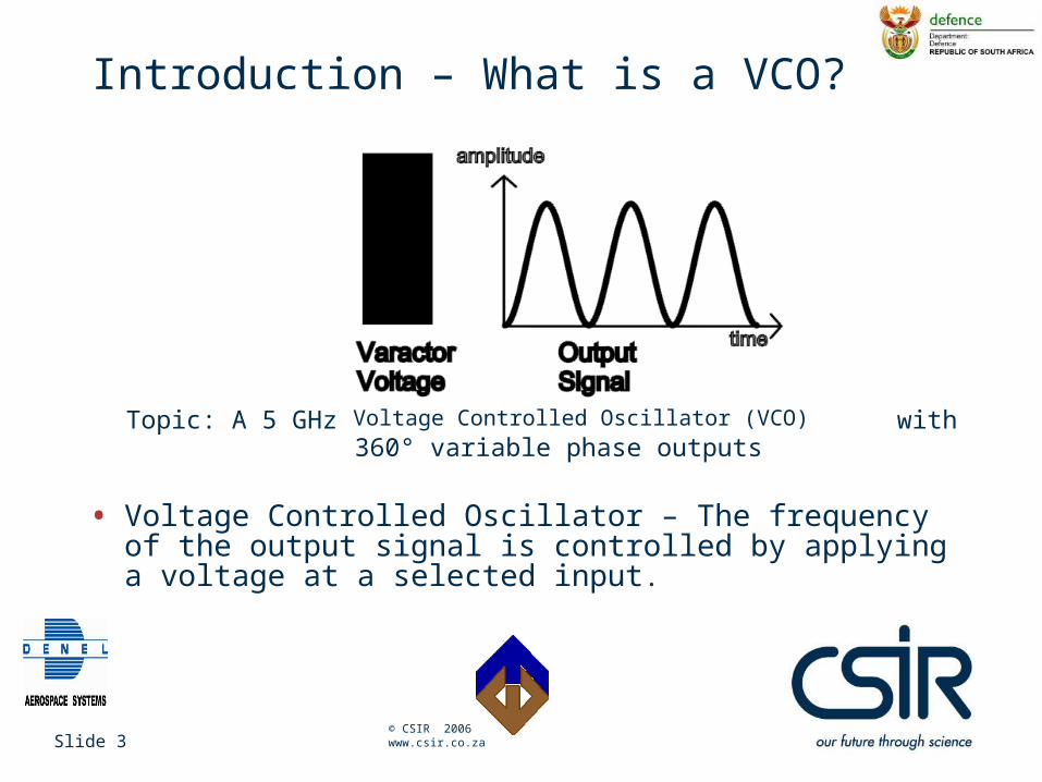
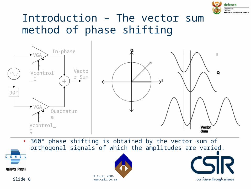
• Introduction• Motivation for Design• Methods of Phase Shifting• Design Specifications and Goals• Circuit Realization and Simulation Results• Circuit Layout• Integration with Modern Modulation Schemes• Summary• Questions/Comments?

Slide 3 © CSIR 2006 www.csir.co.za

Introduction – What is a VCO?

• Voltage Controlled Oscillator – The frequency of the output signal is controlled by applying a voltage at a selected input.

Topic: A 5 GHz Voltage Controlled Oscillator (VCO) with 360° variable phase outputs

Voltage Controlled Oscillator (VCO)

Slide 4 © CSIR 2006 www.csir.co.za

Introduction – What is meant by phase-shifting?

• Phase shifting - When a signal is being delayed for a certain time causing it to be out of phase by a certain angle with a reference signal.

Topic: A 5 GHz Voltage Controlled Oscillator (VCO) with 360° variable phase outputsvariable phase outputs

Slide 5 © CSIR 2006 www.csir.co.za

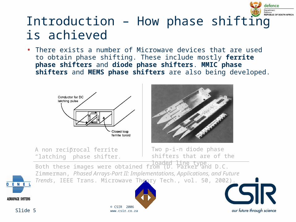
Introduction – How phase shifting is achieved• There exists a number of Microwave devices that are used to

obtain phase shifting. These include mostly ferrite phase shifters and diode phase shifters. MMIC phase shifters and MEMS phase shifters are also being developed.

A non reciprocal ferrite “latching” phase shifter.

Two p-i-n diode phase shifters that are of the loaded line type.

Both these images were obtained from (D. Parker and D.C. Zimmerman, Phased Arrays-Part II: Implementations, Applications, and Future Trends, IEEE Trans. Microwave Theory Tech., vol. 50, 2002).

Slide 6 © CSIR 2006 www.csir.co.za

Introduction – The vector sum method of phase shifting

• 360° phase shifting is obtained by the vector sum of orthogonal signals of which the amplitudes are varied.

Vector Sum

90°

VGA

VGA

+

In-phase

Quadrature

Vcontrol_I

Vcontrol_Q

+ -

+ -

Slide 7 © CSIR 2006 www.csir.co.za

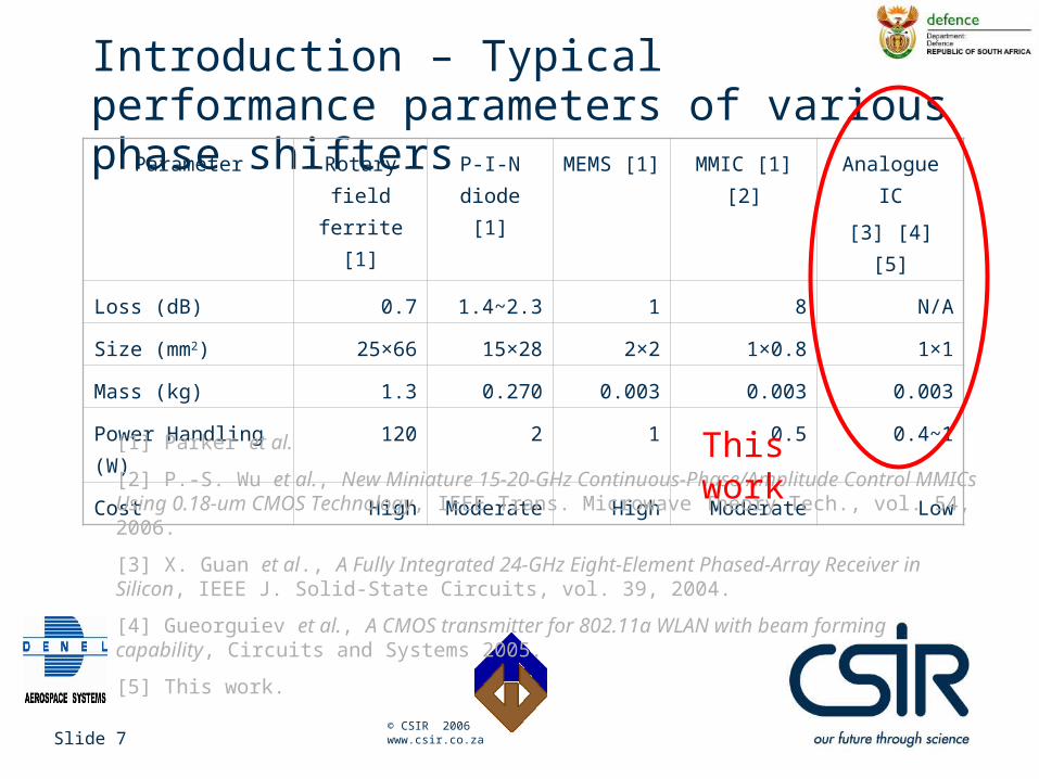
Introduction – Typical performance parameters of various phase shifters

Parameter Rotary field

ferrite [1]

P-I-N diode

[1]

MEMS [1] MMIC [1] [2] Analogue IC

[3] [4] [5]

Loss (dB) 0.7 1.4~2.3 1 8 N/A

Size (mm2) 25×66 15×28 2×2 1×0.8 1×1

Mass (kg) 1.3 0.270 0.003 0.003 0.003

Power Handling (W) 120 2 1 0.5 0.4~1

Cost High Moderate High Moderate Low

[1] Parker et al.

[2] P.-S. Wu et al., New Miniature 15-20-GHz Continuous-Phase/Amplitude Control MMICs Using 0.18-um CMOS Technology, IEEE Trans. Microwave Theory Tech., vol. 54, 2006.

[3] X. Guan et al., A Fully Integrated 24-GHz Eight-Element Phased-Array Receiver in Silicon, IEEE J. Solid-State Circuits, vol. 39, 2004.

[4] Gueorguiev et al., A CMOS transmitter for 802.11a WLAN with beam forming capability, Circuits and Systems 2005.

[5] This work.

This work

Slide 8 © CSIR 2006 www.csir.co.za

Motivation for Design

• Single-element linear antennas tend to spread radiated power over the broad beams in their radiation patterns.

• An array of antenna elements can be used to control the directionality of the radiation pattern.

• This architecture is mostly applied to RADAR systems and could be beneficial towards communications systems as well (e.g. smart antennas).

A giant phased-array RADAR in Alaska, USA

- Antenna Arrays

Slide 9 © CSIR 2006 www.csir.co.za

Motivation for Design - Antenna Arrays

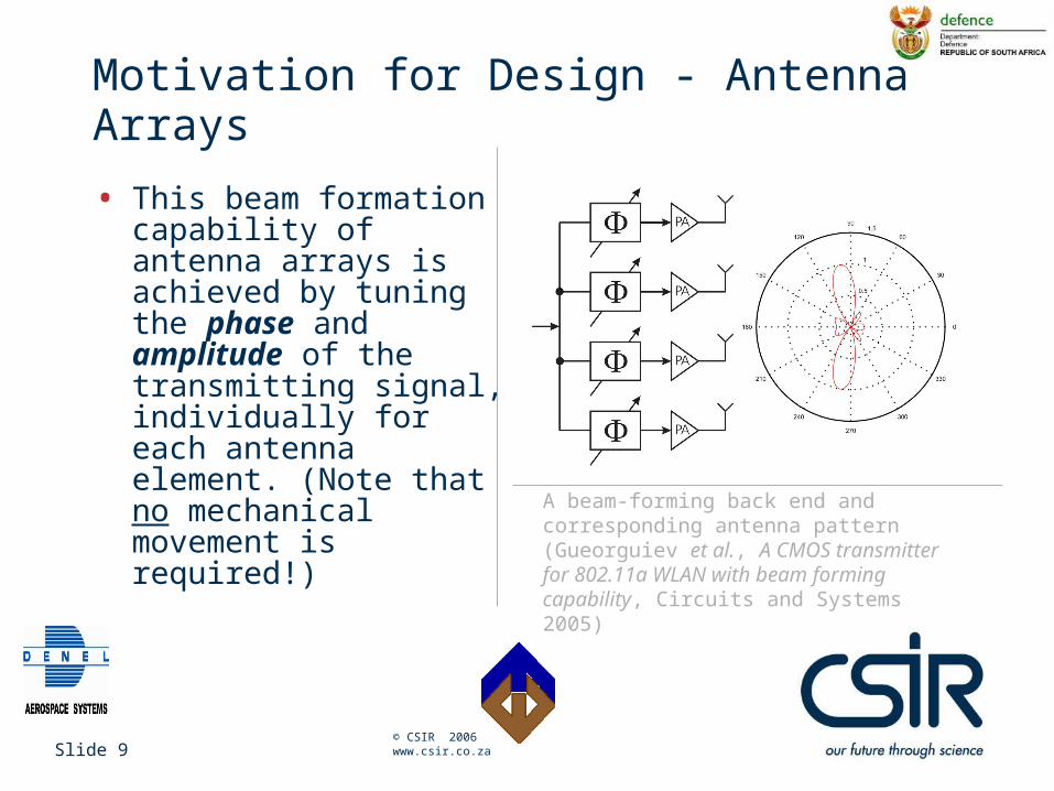
• This beam formation capability of antenna arrays is achieved by tuning the phase and amplitude of the transmitting signal, individually for each antenna element. (Note that no mechanical movement is required!) A beam-forming back end and corresponding

antenna pattern (Gueorguiev et al., A CMOS transmitter for 802.11a WLAN with beam forming capability, Circuits and Systems 2005)

Slide 10 © CSIR 2006 www.csir.co.za

Design Specifications and Goals (2007)

1. To design a quadrature VCO with a tuning range of 4.6 to 5.3 GHz.

2. The VCO must have multiple outputs and the phase shift of each output must be independently variable over its entire cycle (i.e. 360°).

3. The phase shifting must be accomplished using the vector sum method.

4. The entire design must be implemented on an Integrated Circuit (IC) using the AMS S35 SiGe BiCMOS process.

Slide 11 © CSIR 2006 www.csir.co.za

Design Specifications and Goals (2008)

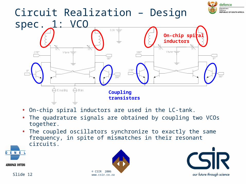
5. The design must be fabricated through Europractice (which is also a requirement for the Master’s degree: Micro-Electronic Engineering, University of Pretoria).

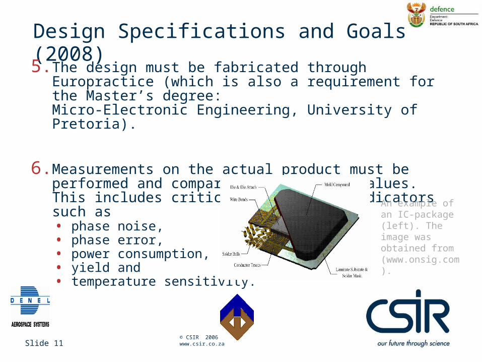
6. Measurements on the actual product must be performed and compared to predicted values. This includes critical performance indicators such as• phase noise, • phase error,• power consumption,• yield and • temperature sensitivity.

An example of an IC-package (left). The image was obtained from (www.onsig.com).

Slide 12 © CSIR 2006 www.csir.co.za

Circuit Realization – Design spec. 1: VCO

• On-chip spiral inductors are used in the LC-tank.• The quadrature signals are obtained by coupling two VCOs

together.• The coupled oscillators synchronize to exactly the same

frequency, in spite of mismatches in their resonant circuits.

Vtune

IBiasICoupling

3.3V

Vtune

90°

180°

180°

90°

270°

270°

On-chip spiral inductors

Coupling transistors

Slide 13 © CSIR 2006 www.csir.co.za

0 0.5 1 1.5 2 2.5 34.2

4.4

4.6

4.8

5

5.2

5.4x 10

9

Vtune (V)

Out

put F

requ

ency

(H

z)

Tuning characteristic of the VCO

Simulation Results – Design spec. 1: VCO

• Simulation results show that this design specification has been achieved.

Out

put

Fre

quen

cy (

GH

z)

Slide 14 © CSIR 2006 www.csir.co.za

Circuit Realization – Design spec. 2 and 3: Phase shifter

• The schematic of the Gilbert Mixer used for a Variable Gain Amplifier (VGA).

• The current of the mixers are combined to obtain the vector sum.• The differential architecture of the Mixer requires the transistors used as

current sources to be closely matched.

Vcontrol-

Vcontrol+

Isum- Isum+

Vosc-

Vosc+

Gilbert Mixer

Gilbert Mixer

Vector Sum

90°

VGA

VGA

+

In-phase

Quadrature

Vcontrol_I

Vcontrol_Q

+ -

+ -

Slide 15 © CSIR 2006 www.csir.co.za

Simulation Results – Design spec. 2 and 3: Phase shifter

• The quadrature amplitude was held constant while the in-phase voltage amplitude was swept.

• The phase shift was then measured.

Slide 16 © CSIR 2006 www.csir.co.za

Simulation Results – Design spec. 2 and 3: Phase shifter

• Since the quadrature amplitude was held constant, the vector sum amplitude decreased by a factor of .2

Slide 17 © CSIR 2006 www.csir.co.za

Circuit Layout

A cross section of the AMS S35 SiGe BiCMOS process wafer. This image was obtained from (AustriaMicroSystems, 0.35μm HBT BiCMOS Process Parameters, ENG-219, Rev. 4.0)

Slide 18 © CSIR 2006 www.csir.co.za

Circuit Layout

Key features of the AMS S35 process:

• Triple poly, triple metal process + 1 thick metal layer• SiGe BiCMOS Mixed Signal and RF transistors• Poly-Poly and Metal-Metal capacitors• Feature sizes: 0.35 μm gates and 0.4 μm emitters• Supply voltage 3.3V / 5.5V• ft > 60 GHz and fmax > 70 GHz• BVceo > 2V

• 2007 Prototyping cost through Europractice: 1000 EURO/mm2 • Minimum required size for prototyping: 5 mm2

Slide 19 © CSIR 2006 www.csir.co.za

Circuit Layout• The physical layout of the VCO

(right) and the Gilbert Mixer (below). The complete design is to be fabricated in 2008.

Slide 20 © CSIR 2006 www.csir.co.za

Integration with Modern Modulation Systems

• The vector sum method creates a variable phase offset on the harmonic signal it has produced.

• The vector sum method therefore does not shift the phase of an incoming signal as with conventional phase shifters.

• The most straight forward application for this kind of phase shifter would be to transmit information using Frequency-Shift Keying (FSK).

Data

Phase shifter 1

Phase shifter 2

Phase shifter n

90°

Frequency control

PA1

PA2

PAn

Slide 21 © CSIR 2006 www.csir.co.za

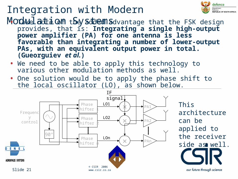
Integration with Modern Modulation Systems• Take note of the added advantage that the FSK design provides,

that is: Integrating a single high-output power amplifier (PA) for one antenna is less favorable than integrating a number of lower-output PAs, with an equivalent output power in total. (Gueorguiev et al.)

• We need to be able to apply this technology to various other modulation methods as well.

• One solution would be to apply the phase shift to the local oscillator (LO), as shown below.

This architecture can be applied to the receiver side as well.

Phase shifter 1

Phase shifter 2

Phase shifter n

90°

Frequency control

PA1

PA2

PAn

×

×

×

IF signal

LO1

LO2

LOn

Slide 22 © CSIR 2006 www.csir.co.za

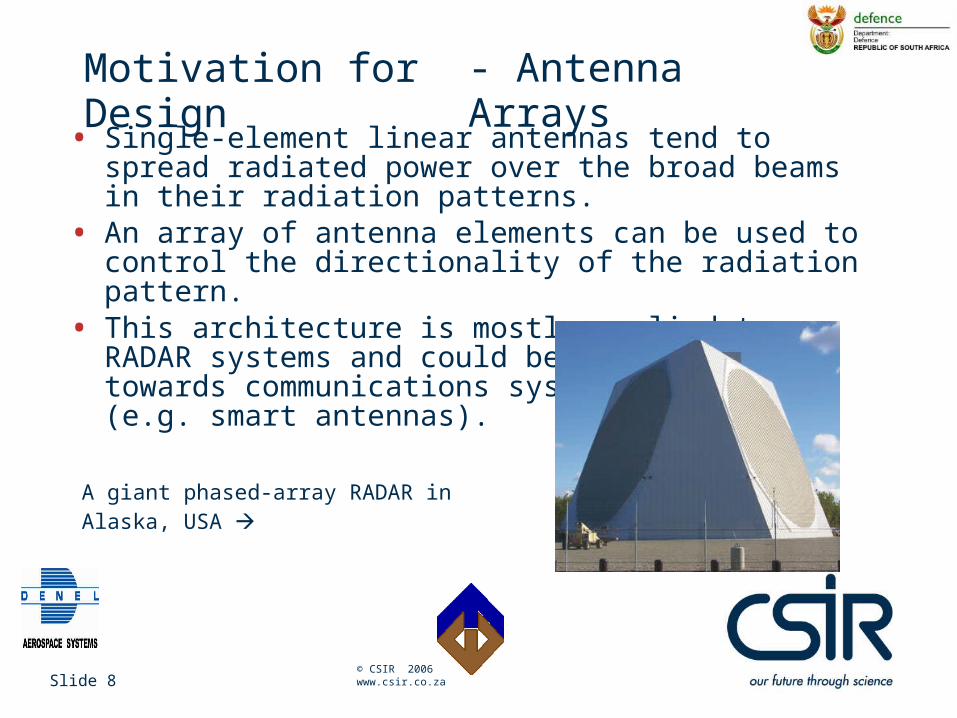
Summary• Beam-forming allows the transmitter to transmit less power to

cover the same distance and this is achieved with the aid of phase shifters.

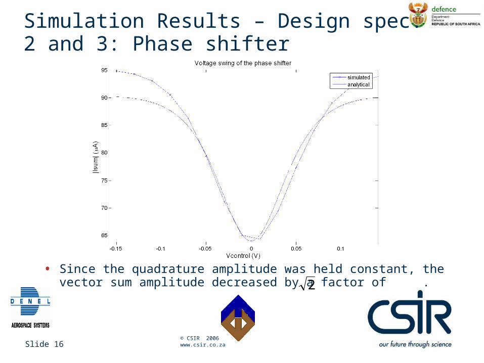
• Although the Analogue IC vector sum phase shifter has much lower power handling capability than most microwave phase shifters, it is much smaller, cheaper (when mass produced) and can adapt very quickly.

• Such an IC has been designed and simulated operating at 5 GHz. It is worth investigating the application of this technology for a low cost, portable C-band RADAR (the CSIR and the DoD could benefit from this).

• Instead of having to integrate a single high-output PA for only one antenna, with phased-arrays it is possible to integrate multiple lower-output PAs.

Slide 23 © CSIR 2006 www.csir.co.za

Questions/Comments?


Recommended