Page 1
A 51x51 Multiplier Design Based on Signed
18x18 and Unsigned 17x17 Multipliers
Jonathan Roth and Hani Mehrpouyan
Department of Electrical and Computer Engineering
Queen’s University, Kingston, Ontario, K7L3N6, Canada
Abstract
This report provides a brief overview of the two popular schemes of performing large operand
multiplication, sign extension and Baugh-Wolley’s algorithm, and provides the implementation and
performance analysis for an unsigned 17x17 and a signed 18x18 multiplier. Furthermore, an efficient
scheme for combining the unsigned 17x17 or signed 18x18 multipliers is used to implement two different
versions of a signed 51x51 multiplier and comparative analysis between the two methods is included,
where the area, speed, and power consumption of the two schemes are compared. VHDL and synopsis
are used to implement the logic blocks and layout of the 51x51 signed multiplier, respectively.
I. INTRODUCTION
In recent years, modern FPGAs contain large number of embedded blocks, such as embedded
multipliers and DSP functions ([1] and [2]).
The availability of many efficient and optimized embedded logic blocks within today’s Field
Programable Gate Arrays (FPGAs) has greatly facilitated the design process for more complicated
logic functions [1], [2]. Large multipliers are an example of such complicated functions with
many applications in signal processing, fast fourier transform (FFT), and image processing ([3]
and [4]). Therefore, there have been many schemes proposed to design larger size multipliers
from smaller ones. The divide-and-conquer strategy presented in [5] has been used to realize
matrix multiplication based on word-width decomposition. The broadcast algorithm was proposed
in [6] which is sequential and requires less resources at the cost of a slower speed. The sliding
window scheme, [7], has been reported to efficiently realize large size multipliers. The algorithm
generates less partial products by skipping zeros in the operand. However, it is not efficient for
implementation in FPGAs.
April 15, 2008 DRAFT
Page 2
2
In [8] a new methodology is presented to realize multipliers in FPGAs. This method can
be recursively applied to implement multipliers with large operands. However, the proposed
algorithm is based on the sign extension algorithm which has been demonstrated (in [9]) to be
inefficient compared to Baugh-Wooley’s algorithm for FPGA design. In [10] a new scheme based
on the carry-save multiplier scheme first outlined in [11] is proposed. The algorithm promises to
reduce the total number of cells required in and FPGA and reduce the number of interconnects.
Thus, reducing delay. However, it is important to point out the algorithm does not shed any new
light on how to reduce the overall complexity associated with the multiplication when smaller
blocks are used and it is mainly focused around reducing the number of interconnects within
the different cells of the FPGA.
Baugh-Wooley’s algorithm, [12], is a popular algorithm that can handle block level manip-
ulation. As, it is known, Bough-Wooley’s algorithm performs a transformation of the two’s
complement multiplication into two components, unsigned and signed. In this report we use the
more methodical and structured approach proposed in [9] to come up with the structure of a
51x51 signed multiplier based on 17x17 unsigned and 18x18 signed multipliers. The proposed
scheme in [9], first converts the operands from a two’s complement notation to a sign-magnitude
notation. Secondly, the large unsigned multiplication is carried out on the resulting magnitudes.
Subsequently the result of the multiplication is converted into a two’s complement notation.
The two versions of the signed 51x51 multipliers are implemented using VHDL. The resulting
structure is then laid out using Synopsis and based on the CMOSP18 Artisan (.18µm) technology.
Finally, the speed, layout area, and power consumption of the two different designs for the 51x51
multiplier are comparatively analyzed.
II. SIGN EXTENSION METHOD
The sign extension algorithm is commonly used in the design of large two’s complement
multipliers based on smaller blocks for FPGA implementations. The scheme extends the partial
product in each row based on the sign of the multiplicands.Therefore, a disadvantages of the sign
extension method is that smaller blocks of unsigned multipliers can not be used to determine
larger ones.
1The VHDL code for both designs was first compiled using Quartus II software provided by Altera [13].
April 15, 2008 DRAFT
Page 3
3
The first step partitions the large size operands of the multiplier into smaller size segments.
In general using n− bit wide embedded blocks, the operands A and B are decomposed into m
segments.
A = [Am−1, Am−2...A1, A0]2n
B = [Bm−1, Bm−2...B1, B0]2n,
(1)
where only the most significant segments, Am−1 and Bm−1 take the sign bits of A and B,
respectively. Therefore, all other segments can be treated as positive numbers and A and B can
be represented as
A = 2(m−1)nAm−1 + 2(m−2)nAm−2 + ... + 2nA1 + A0
B = 2(m−1)nBm−1 + 2(m−2)nBm−2 + ... + 2nB1 + B0.(2)
To correctly exploit the signed multiplier for the positive number multiplication, the sign bits
of the embedded multipliers have to be forced to 0. To illustrate the process involved better the
design of a 35x35 bit multiplier based on smaller blocks of signed 18x18 multipliers is discussed
here. In this scenario, the number of segments m is equal to 2 and the bit size of the positive
number multiplication is 1717. The input operands are
A = [A1A0]2n
B = [B1B0]2n,
(3)
where A1 and B1 are the most significant bit positions and A0 and B0 are the least significant
bit positions of A and B, respectively.
A×B = [A12n + A0]× [B12
n + B0]
= A1B122n + A0B0 + A1B02
n + A0B12n
(4)
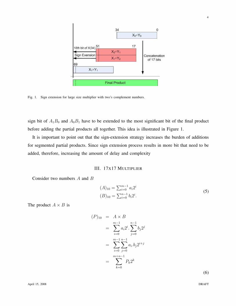
The first partial product in Equation (4) is A1B122n, which requires no sign extension because
the sign is already embedded in both A1 and B1. The second partial product, A0×B0, is also an
unsigned multiplication and again does not require sign extension. The last two partial products
in Equation (4) are A1B02n and A0B12
n. Since A1 and B1 keep the sign of the operands A
and B and A0 and B0 are positive numbers, the partial products A1B0 or B1A0 have exactly the
same sign as that of A1 and B1, which is also the sign of A and B, respectively. Therefore the
April 15, 2008 DRAFT
Page 4
4
Fig. 1. Sign extension for large size multiplier with two’s complement numbers.
sign bit of A1B0 and A0B1 have to be extended to the most significant bit of the final product
before adding the partial products all together. This idea is illustrated in Figure 1.
It is important to point out that the sign-extension strategy increases the burden of additions
for segmented partial products. Since sign extension process results in more bit that need to be
added, therefore, increasing the amount of delay and complexity
III. 17X17 MULTIPLIER
Consider two numbers A and B
(A)10 =∑m−1
i=0 ai2i
(B)10 =∑n−1
i=0 bi2i.
(5)
The product A×B is
(P )10 = A×B
=m−1∑i=0
ai2i.
n−1∑j=0
bj2j
=m−1∑i=0
n−1∑j=0
ai.bj2i+j
=m+n−1∑
k=0
Pk2k
(6)
April 15, 2008 DRAFT
Page 5
5
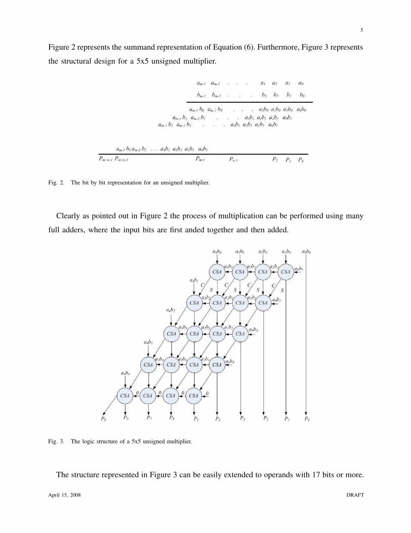
Figure 2 represents the summand representation of Equation (6). Furthermore, Figure 3 represents
the structural design for a 5x5 unsigned multiplier.
Fig. 2. The bit by bit representation for an unsigned multiplier.
Clearly as pointed out in Figure 2 the process of multiplication can be performed using many
full adders, where the input bits are first anded together and then added.
Fig. 3. The logic structure of a 5x5 unsigned multiplier.
The structure represented in Figure 3 can be easily extended to operands with 17 bits or more.
April 15, 2008 DRAFT
Page 6
6
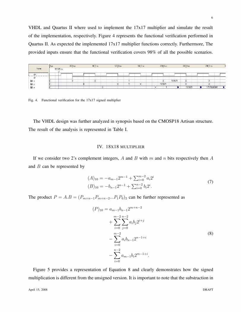
VHDL and Quartus II where used to implement the 17x17 multiplier and simulate the result
of the implementation, respectively. Figure 4 represents the functional verification performed in
Quartus II. As expected the implemented 17x17 multiplier functions correctly. Furthermore, The
provided inputs ensure that the functional verification covers 98% of all the possible scenarios.
Fig. 4. Functional verification for the 17x17 signed multiplier
The VHDL design was further analyzed in synopsis based on the CMOSP18 Artisan structure.
The result of the analysis is represented in Table I.
IV. 18X18 MULTIPLIER
If we consider two 2’s complement integers, A and B with m and n bits respectively then A
and B can be represented by
(A)10 = −am−12m−1 +
∑m−2i=0 ai2
i
(B)10 = −bn−12n−1 +
∑n−2i=0 bi2
i.(7)
The product P = A.B = (Pm+n−1Pm+n−2...P1P0)2 can be further represented as
(P )10 = am−1bn−12m+n−2
+m−2∑i=0
n−2∑j=0
aibj2i+j
−m−2∑i=0
aibn−12n−1+i
−n−2∑i=0
am−1bi2m−1+i.
(8)
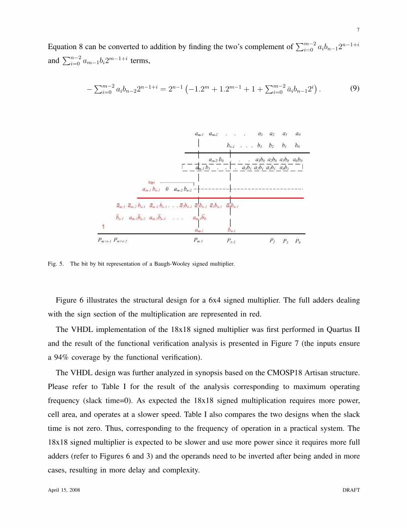
Figure 5 provides a representation of Equation 8 and clearly demonstrates how the signed
multiplication is different from the unsigned version. It is important to note that the substraction in
April 15, 2008 DRAFT
Page 7
7
Equation 8 can be converted to addition by finding the two’s complement of∑m−2
i=0 aibn−12n−1+i
and∑n−2
i=0 am−1bi2m−1+i terms,
−∑m−2i=0 aibn−22
n−1+i = 2n−1(−1.2m + 1.2m−1 + 1 +
∑m−2i=0 aibn−12
i). (9)
Fig. 5. The bit by bit representation of a Baugh-Wooley signed multiplier.
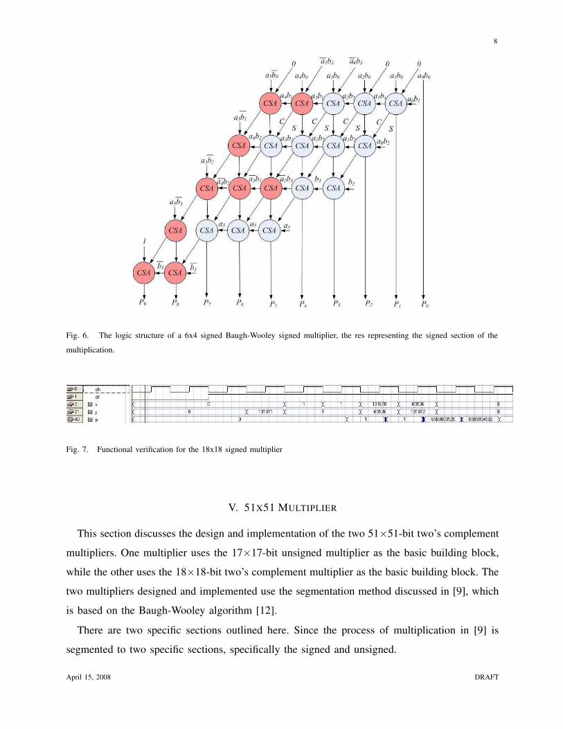
Figure 6 illustrates the structural design for a 6x4 signed multiplier. The full adders dealing
with the sign section of the multiplication are represented in red.
The VHDL implementation of the 18x18 signed multiplier was first performed in Quartus II
and the result of the functional verification analysis is presented in Figure 7 (the inputs ensure
a 94% coverage by the functional verification).
The VHDL design was further analyzed in synopsis based on the CMOSP18 Artisan structure.
Please refer to Table I for the result of the analysis corresponding to maximum operating
frequency (slack time=0). As expected the 18x18 signed multiplication requires more power,
cell area, and operates at a slower speed. Table I also compares the two designs when the slack
time is not zero. Thus, corresponding to the frequency of operation in a practical system. The
18x18 signed multiplier is expected to be slower and use more power since it requires more full
adders (refer to Figures 6 and 3) and the operands need to be inverted after being anded in more
cases, resulting in more delay and complexity.
April 15, 2008 DRAFT
Page 8
8
Fig. 6. The logic structure of a 6x4 signed Baugh-Wooley signed multiplier, the res representing the signed section of the
multiplication.
Fig. 7. Functional verification for the 18x18 signed multiplier
V. 51X51 MULTIPLIER
This section discusses the design and implementation of the two 51×51-bit two’s complement
multipliers. One multiplier uses the 17×17-bit unsigned multiplier as the basic building block,
while the other uses the 18×18-bit two’s complement multiplier as the basic building block. The
two multipliers designed and implemented use the segmentation method discussed in [9], which
is based on the Baugh-Wooley algorithm [12].
There are two specific sections outlined here. Since the process of multiplication in [9] is
segmented to two specific sections, specifically the signed and unsigned.
April 15, 2008 DRAFT
Page 9
9
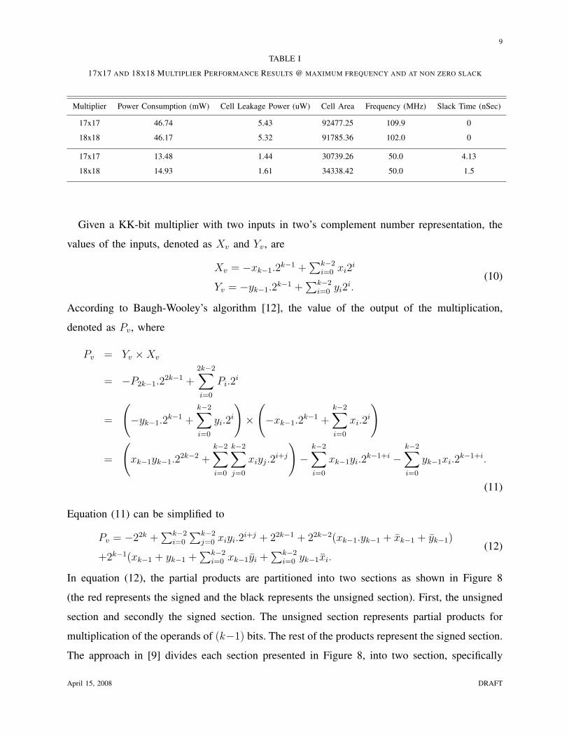
TABLE I
17X17 AND 18X18 MULTIPLIER PERFORMANCE RESULTS @ MAXIMUM FREQUENCY AND AT NON ZERO SLACK
Multiplier Power Consumption (mW) Cell Leakage Power (uW) Cell Area Frequency (MHz) Slack Time (nSec)
17x17 46.74 5.43 92477.25 109.9 0
18x18 46.17 5.32 91785.36 102.0 0
17x17 13.48 1.44 30739.26 50.0 4.13
18x18 14.93 1.61 34338.42 50.0 1.5
Given a KK-bit multiplier with two inputs in two’s complement number representation, the
values of the inputs, denoted as Xv and Yv, are
Xv = −xk−1.2k−1 +
∑k−2i=0 xi2
i
Yv = −yk−1.2k−1 +
∑k−2i=0 yi2
i.(10)
According to Baugh-Wooley’s algorithm [12], the value of the output of the multiplication,
denoted as Pv, where
Pv = Yv ×Xv
= −P2k−1.22k−1 +
2k−2∑i=0
Pi.2i
=
(−yk−1.2
k−1 +k−2∑i=0
yi.2i
)×
(−xk−1.2
k−1 +k−2∑i=0
xi.2i
)
=
(xk−1yk−1.2
2k−2 +k−2∑i=0
k−2∑j=0
xiyj.2i+j
)−
k−2∑i=0
xk−1yi.2k−1+i −
k−2∑i=0
yk−1xi.2k−1+i.
(11)
Equation (11) can be simplified to
Pv = −22k +∑k−2
i=0
∑k−2j=0 xiyi.2
i+j + 22k−1 + 22k−2(xk−1.yk−1 + xk−1 + yk−1)
+2k−1(xk−1 + yk−1 +∑k−2
i=0 xk−1yi +∑k−2
i=0 yk−1xi.(12)
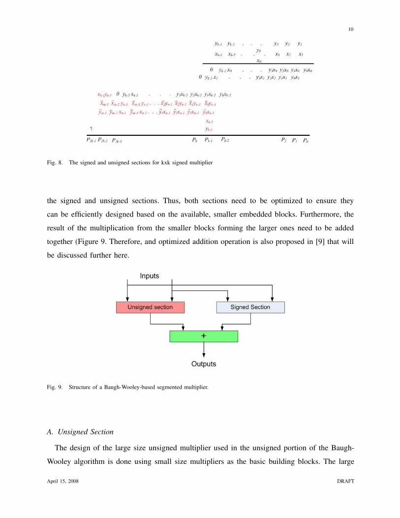
In equation (12), the partial products are partitioned into two sections as shown in Figure 8
(the red represents the signed and the black represents the unsigned section). First, the unsigned
section and secondly the signed section. The unsigned section represents partial products for
multiplication of the operands of (k−1) bits. The rest of the products represent the signed section.
The approach in [9] divides each section presented in Figure 8, into two section, specifically
April 15, 2008 DRAFT
Page 10
10
Fig. 8. The signed and unsigned sections for kxk signed multiplier
the signed and unsigned sections. Thus, both sections need to be optimized to ensure they
can be efficiently designed based on the available, smaller embedded blocks. Furthermore, the
result of the multiplication from the smaller blocks forming the larger ones need to be added
together (Figure 9. Therefore, and optimized addition operation is also proposed in [9] that will
be discussed further here.
Fig. 9. Structure of a Baugh-Wooley-based segmented multiplier.
A. Unsigned Section
The design of the large size unsigned multiplier used in the unsigned portion of the Baugh-
Wooley algorithm is done using small size multipliers as the basic building blocks. The large
April 15, 2008 DRAFT
Page 11
11
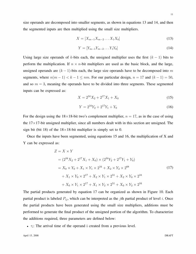
size operands are decomposed into smaller segments, as shown in equations 13 and 14, and then
the segmented inputs are then multiplied using the small size multipliers.
X = [Xm−1Xm−2 . . . X1X0] (13)
Y = [Ym−1Ym−2 . . . Y1Y0] (14)
Using large size operands of k-bits each, the unsigned multiplier uses the first (k − 1) bits to
perform the multiplication. If n × n-bit multipliers are used as the basic block, and the large,
unsigned operands are (k− 1)-bits each, the large size operands have to be decomposed into m
segments, where n(m− 1) < k − 1 ≤ nm. For our particular design, n = 17 and (k − 1) = 50,
and so m = 3, meaning the operands have to be divided into three segments. These segmented
inputs can be expressed as:
X = 234X2 + 217X1 + X0 (15)
Y = 234Y2 + 217Y1 + Y0 (16)
For the design using the 18×18-bit two’s complement multiplier, n = 17, as in the case of using
the 17×17-bit unsigned multiplier, since all numbers dealt with in this section are unsigned. The
sign bit (bit 18) of the 18×18-bit multiplier is simply set to 0.
Once the inputs have been segmented, using equations 15 and 16, the multiplication of X and
Y can be expressed as:
Z = X × Y
= (234X2 + 217X1 + X0)× (234Y2 + 217Y1 + Y0)
= X0 × Y0 + X1 × Y1 × 234 + X2 × Y2 × 268
+ X1 × Y0 × 217 + X2 × Y1 × 251 + X2 × Y0 × 234
+ X0 × Y1 × 217 + X1 × Y2 × 251 + X0 × Y2 × 234
(17)
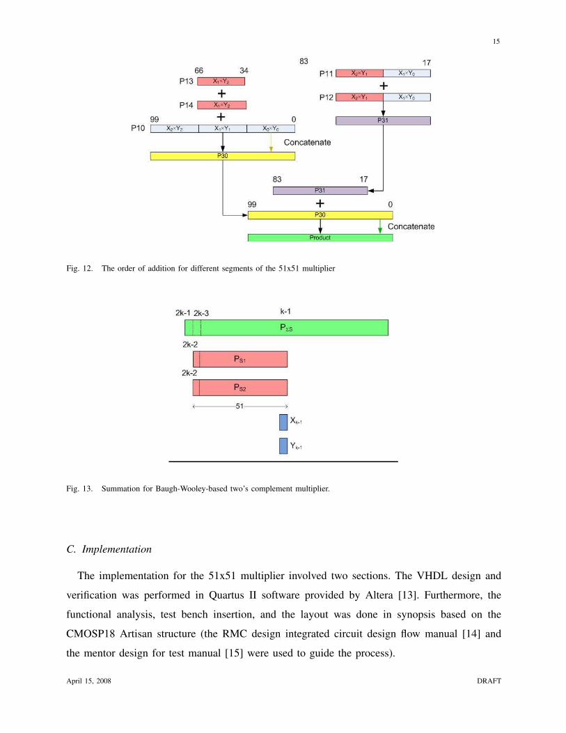
The partial products generated by equation 17 can be organized as shown in Figure 10. Each
partial product is labeled Pij , which can be interpreted as the jth partial product of level i. Once
the partial products have been generated using the small size multipliers, additions must be
performed to generate the final product of the unsigned portion of the algorithm. To characterize
the additions required, three parameters are defined below:
• τi: The arrival time of the operand i created from a previous level.
April 15, 2008 DRAFT
Page 12
12
• δij: The execution delay created by adding the operands i and j at the current level.
• ∆ij: The accumulated delay that is the total value of the arrival time and the execution
delay at the current level, which is also the arrival time for the next level.
The execution delay is assumed to only depend on the operand size and relative offset of the
operands, and can be calculated as:
δij = max(size(i), size(j))− abs(offset(i)− offset(j)) (18)
Also, the accumulated delay is calculated as:
∆ij = max(τi, τj) + δij (19)
Fig. 10. The multiplication segmentation for the 51x51 multiplier
The first level of additions involve adding the partial products that are of the same length.
Referring to Figure 10, the first level includes the addition of P11 and P12, and the addition
of P13 and P14. The second and third level of additions are organized taking into account the
arrival times of the partial products from the previous level. The second level partial products
to be added are P20, which is the same as P10, P21, which is the addition of P11 and P12, and
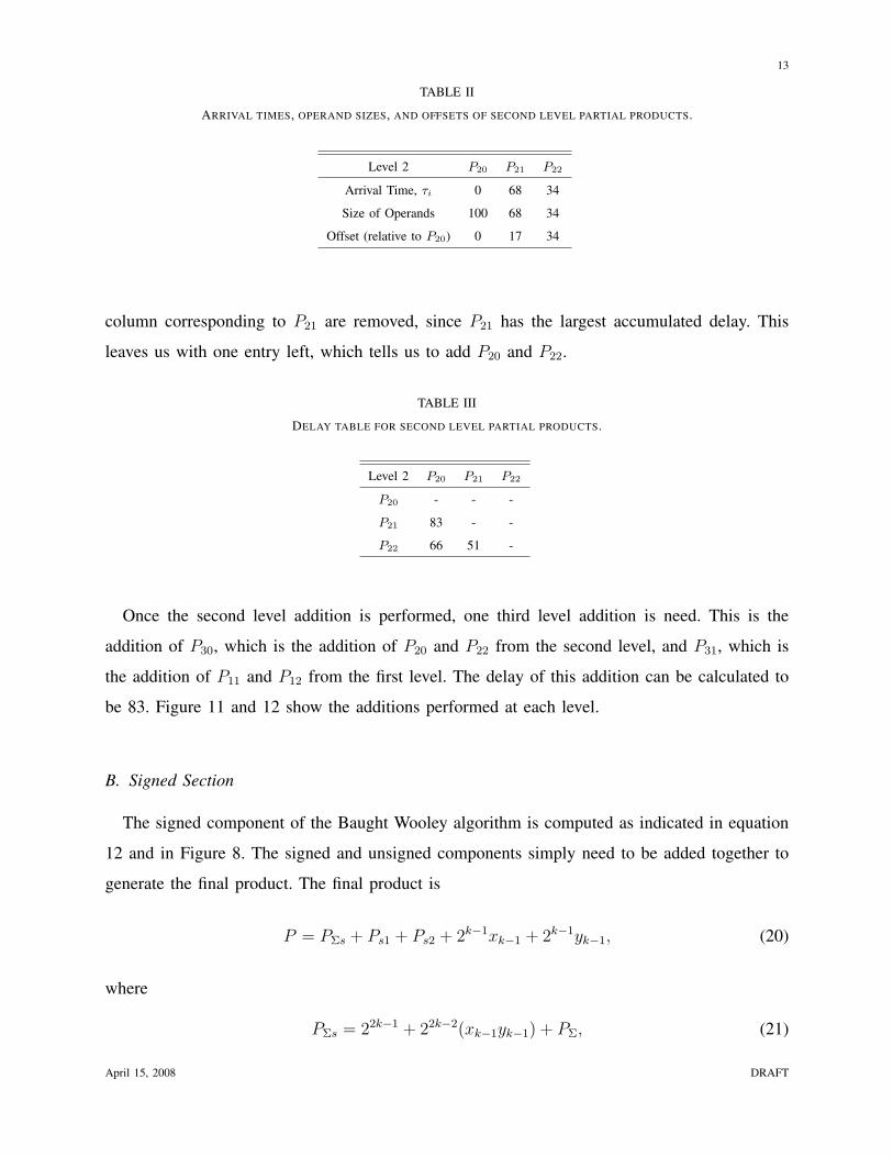
P22, which is the addition of P13 and P14. Table II shows the arrival times, operand sizes, and
offsets of the second level partial products.
A delay table, table III, for the addition of the second level operands is also created, which
shows the accumulated delay of adding operands i and j, ∆ij . From the algorithm, the row and
April 15, 2008 DRAFT
Page 13
13
TABLE II
ARRIVAL TIMES, OPERAND SIZES, AND OFFSETS OF SECOND LEVEL PARTIAL PRODUCTS.
Level 2 P20 P21 P22
Arrival Time, τi 0 68 34
Size of Operands 100 68 34
Offset (relative to P20) 0 17 34
column corresponding to P21 are removed, since P21 has the largest accumulated delay. This
leaves us with one entry left, which tells us to add P20 and P22.
TABLE III
DELAY TABLE FOR SECOND LEVEL PARTIAL PRODUCTS.
Level 2 P20 P21 P22
P20 - - -
P21 83 - -
P22 66 51 -
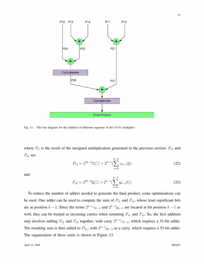
Once the second level addition is performed, one third level addition is need. This is the
addition of P30, which is the addition of P20 and P22 from the second level, and P31, which is
the addition of P11 and P12 from the first level. The delay of this addition can be calculated to
be 83. Figure 11 and 12 show the additions performed at each level.
B. Signed Section
The signed component of the Baught Wooley algorithm is computed as indicated in equation
12 and in Figure 8. The signed and unsigned components simply need to be added together to
generate the final product. The final product is
P = PΣs + Ps1 + Ps2 + 2k−1xk−1 + 2k−1yk−1, (20)
where
PΣs = 22k−1 + 22k−2(xk−1yk−1) + PΣ, (21)
April 15, 2008 DRAFT
Page 14
14
Fig. 11. The tree diagram for the addition of different segments of the 51x51 multiplier
where PΣ is the result of the unsigned multiplication generated in the previous section. Ps1 and
Ps2 are
Ps1 = 22k−2xk−1 + 2k−1(k−2∑i=0
xk−1yi) (22)
and
Ps2 = 22k−2yk−1 + 2k−1(k−2∑i=0
yk−1xi). (23)
To reduce the number of adders needed to generate the final product, some optimizations can
be used. One adder can be used to compute the sum of Ps1 and Ps2, whose least significant bits
are at position k− 1. Since the terms 2k−1xk−1 and 2k−1yk−1 are located at bit position k− 1 as
well, they can be treated as incoming carries when summing Ps1 and Ps2. So, the first addition
step involves adding Ps1 and Ps2 together, with carry 2k−1xk−1, which requires a 51-bit adder.
The resulting sum is then added to PΣs, with 2k−1yk−1 as a carry, which requires a 52-bit adder.
The organization of these sums is shown in Figure 13.
April 15, 2008 DRAFT
Page 15
15
Fig. 12. The order of addition for different segments of the 51x51 multiplier
Fig. 13. Summation for Baugh-Wooley-based two’s complement multiplier.
C. Implementation
The implementation for the 51x51 multiplier involved two sections. The VHDL design and
verification was performed in Quartus II software provided by Altera [13]. Furthermore, the
functional analysis, test bench insertion, and the layout was done in synopsis based on the
CMOSP18 Artisan structure (the RMC design integrated circuit design flow manual [14] and
the mentor design for test manual [15] were used to guide the process).
April 15, 2008 DRAFT
Page 16
16
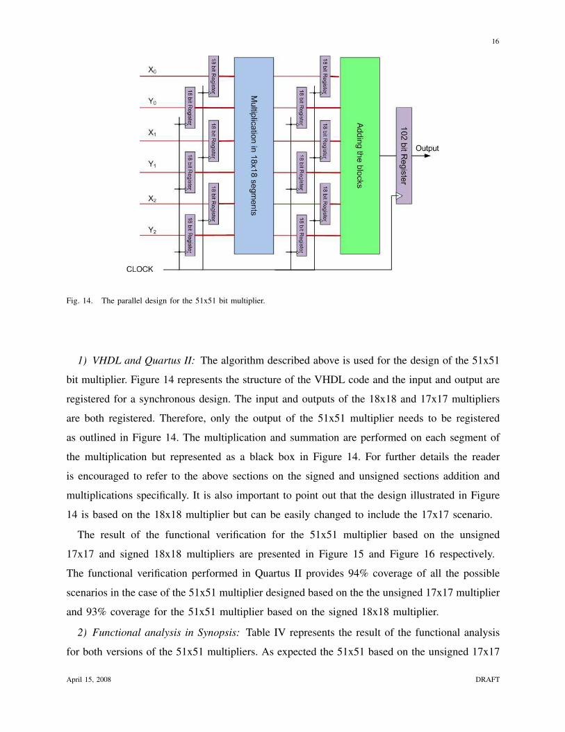
Fig. 14. The parallel design for the 51x51 bit multiplier.
1) VHDL and Quartus II: The algorithm described above is used for the design of the 51x51
bit multiplier. Figure 14 represents the structure of the VHDL code and the input and output are
registered for a synchronous design. The input and outputs of the 18x18 and 17x17 multipliers
are both registered. Therefore, only the output of the 51x51 multiplier needs to be registered
as outlined in Figure 14. The multiplication and summation are performed on each segment of
the multiplication but represented as a black box in Figure 14. For further details the reader
is encouraged to refer to the above sections on the signed and unsigned sections addition and
multiplications specifically. It is also important to point out that the design illustrated in Figure
14 is based on the 18x18 multiplier but can be easily changed to include the 17x17 scenario.
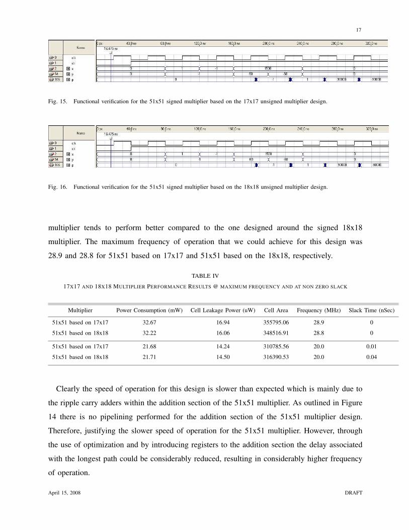
The result of the functional verification for the 51x51 multiplier based on the unsigned
17x17 and signed 18x18 multipliers are presented in Figure 15 and Figure 16 respectively.
The functional verification performed in Quartus II provides 94% coverage of all the possible
scenarios in the case of the 51x51 multiplier designed based on the the unsigned 17x17 multiplier
and 93% coverage for the 51x51 multiplier based on the signed 18x18 multiplier.
2) Functional analysis in Synopsis: Table IV represents the result of the functional analysis
for both versions of the 51x51 multipliers. As expected the 51x51 based on the unsigned 17x17
April 15, 2008 DRAFT
Page 17
17
Fig. 15. Functional verification for the 51x51 signed multiplier based on the 17x17 unsigned multiplier design.
Fig. 16. Functional verification for the 51x51 signed multiplier based on the 18x18 unsigned multiplier design.
multiplier tends to perform better compared to the one designed around the signed 18x18
multiplier. The maximum frequency of operation that we could achieve for this design was
28.9 and 28.8 for 51x51 based on 17x17 and 51x51 based on the 18x18, respectively.
TABLE IV
17X17 AND 18X18 MULTIPLIER PERFORMANCE RESULTS @ MAXIMUM FREQUENCY AND AT NON ZERO SLACK
Multiplier Power Consumption (mW) Cell Leakage Power (uW) Cell Area Frequency (MHz) Slack Time (nSec)
51x51 based on 17x17 32.67 16.94 355795.06 28.9 0
51x51 based on 18x18 32.22 16.06 348516.91 28.8 0
51x51 based on 17x17 21.68 14.24 310785.56 20.0 0.01
51x51 based on 18x18 21.71 14.50 316390.53 20.0 0.04
Clearly the speed of operation for this design is slower than expected which is mainly due to
the ripple carry adders within the addition section of the 51x51 multiplier. As outlined in Figure
14 there is no pipelining performed for the addition section of the 51x51 multiplier design.
Therefore, justifying the slower speed of operation for the 51x51 multiplier. However, through
the use of optimization and by introducing registers to the addition section the delay associated
with the longest path could be considerably reduced, resulting in considerably higher frequency
of operation.
April 15, 2008 DRAFT
Page 18
18
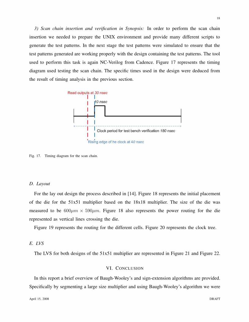
3) Scan chain insertion and verification in Synopsis: In order to perform the scan chain
insertion we needed to prepare the UNIX environment and provide many different scripts to
generate the test patterns. In the next stage the test patterns were simulated to ensure that the
test patterns generated are working properly with the design containing the test patterns. The tool
used to perform this task is again NC-Verilog from Cadence. Figure 17 represents the timing
diagram used testing the scan chain. The specific times used in the design were deduced from
the result of timing analysis in the previous section.
Fig. 17. Timing diagram for the scan chain.
D. Layout
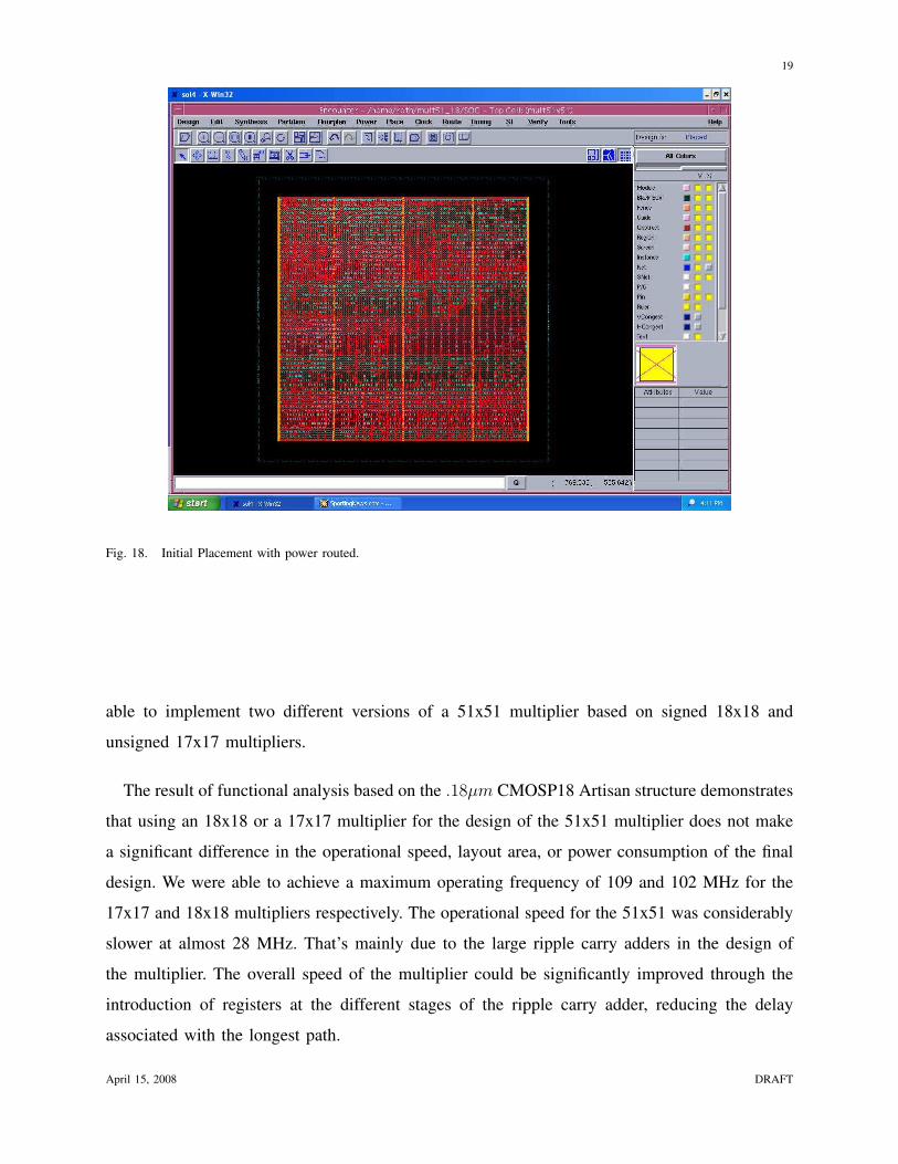
For the lay out design the process described in [14]. Figure 18 represents the initial placement
of the die for the 51x51 multiplier based on the 18x18 multiplier. The size of the die was
measured to be 600µm × 590µm. Figure 18 also represents the power routing for the die
represented as vertical lines crossing the die.
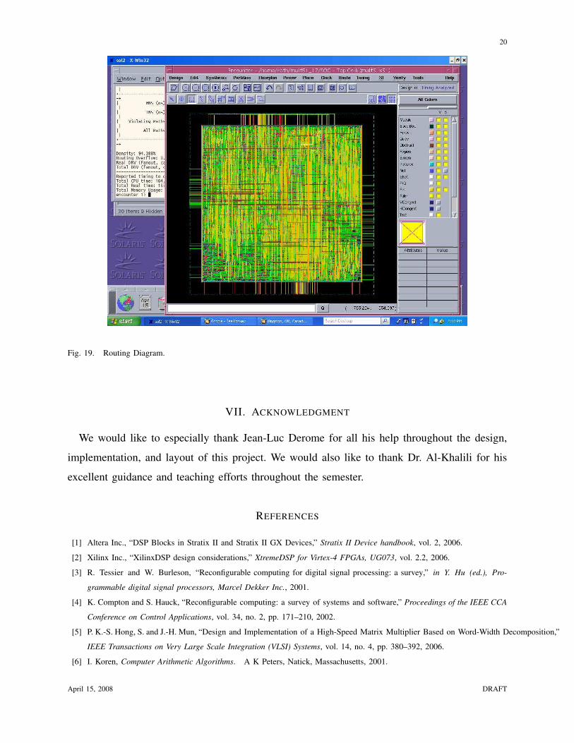
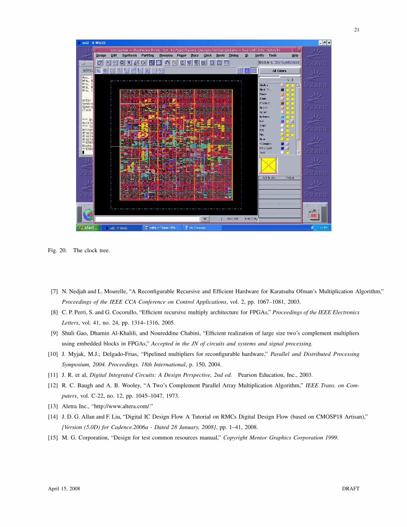
Figure 19 represents the routing for the different cells. Figure 20 represents the clock tree.
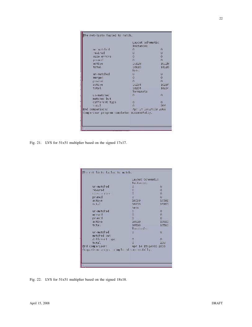
E. LVS
The LVS for both designs of the 51x51 multiplier are represented in Figure 21 and Figure 22.
VI. CONCLUSION
In this report a brief overview of Baugh-Wooley’s and sign-extension algorithms are provided.
Specifically by segmenting a large size multiplier and using Baugh-Wooley’s algorithm we were
April 15, 2008 DRAFT
Page 19
19
Fig. 18. Initial Placement with power routed.
able to implement two different versions of a 51x51 multiplier based on signed 18x18 and
unsigned 17x17 multipliers.
The result of functional analysis based on the .18µm CMOSP18 Artisan structure demonstrates
that using an 18x18 or a 17x17 multiplier for the design of the 51x51 multiplier does not make
a significant difference in the operational speed, layout area, or power consumption of the final
design. We were able to achieve a maximum operating frequency of 109 and 102 MHz for the
17x17 and 18x18 multipliers respectively. The operational speed for the 51x51 was considerably
slower at almost 28 MHz. That’s mainly due to the large ripple carry adders in the design of
the multiplier. The overall speed of the multiplier could be significantly improved through the
introduction of registers at the different stages of the ripple carry adder, reducing the delay
associated with the longest path.
April 15, 2008 DRAFT
Page 20
20
Fig. 19. Routing Diagram.
VII. ACKNOWLEDGMENT
We would like to especially thank Jean-Luc Derome for all his help throughout the design,
implementation, and layout of this project. We would also like to thank Dr. Al-Khalili for his
excellent guidance and teaching efforts throughout the semester.
REFERENCES
[1] Altera Inc., “DSP Blocks in Stratix II and Stratix II GX Devices,” Stratix II Device handbook, vol. 2, 2006.
[2] Xilinx Inc., “XilinxDSP design considerations,” XtremeDSP for Virtex-4 FPGAs, UG073, vol. 2.2, 2006.
[3] R. Tessier and W. Burleson, “Reconfigurable computing for digital signal processing: a survey,” in Y. Hu (ed.), Pro-
grammable digital signal processors, Marcel Dekker Inc., 2001.
[4] K. Compton and S. Hauck, “Reconfigurable computing: a survey of systems and software,” Proceedings of the IEEE CCA
Conference on Control Applications, vol. 34, no. 2, pp. 171–210, 2002.
[5] P. K.-S. Hong, S. and J.-H. Mun, “Design and Implementation of a High-Speed Matrix Multiplier Based on Word-Width Decomposition,”
IEEE Transactions on Very Large Scale Integration (VLSI) Systems, vol. 14, no. 4, pp. 380–392, 2006.
[6] I. Koren, Computer Arithmetic Algorithms. A K Peters, Natick, Massachusetts, 2001.
April 15, 2008 DRAFT
Page 21
21
Fig. 20. The clock tree.
[7] N. Nedjah and L. Mourelle, “A Reconfigurable Recursive and Efficient Hardware for Karatsuba Ofman’s Multiplication Algorithm,”
Proceedings of the IEEE CCA Conference on Control Applications, vol. 2, pp. 1067–1081, 2003.
[8] C. P. Perri, S. and G. Cocorullo, “Efficient recursive multiply architecture for FPGAs,” Proceedings of the IEEE Electronics
Letters, vol. 41, no. 24, pp. 1314–1316, 2005.
[9] Shuli Gao, Dhamin Al-Khalili, and Noureddine Chabini, “Efficient realization of large size two’s complement multipliers
using embedded blocks in FPGAs,” Accepted in the JN of circuits and systems and signal processing.
[10] J. Myjak, M.J.; Delgado-Frias, “Pipelined multipliers for reconfigurable hardware,” Parallel and Distributed Processing
Symposium, 2004. Proceedings. 18th International, p. 150, 2004.
[11] J. R. et al, Digital Integrated Circuits: A Design Perspective, 2nd ed. Pearson Education, Inc., 2003.
[12] R. C. Baugh and A. B. Wooley, “A Two’s Complement Parallel Array Multiplication Algorithm,” IEEE Trans. on Com-
puters, vol. C-22, no. 12, pp. 1045–1047, 1973.
[13] Aletra Inc., “http://www.altera.com/.”
[14] J. D. G. Allan and F. Liu, “Digital IC Design Flow A Tutorial on RMCs Digital Design Flow (based on CMOSP18 Artisan),”
[Version (5.0D) for Cadence.2006a - Dated 28 January, 2008], pp. 1–41, 2008.
[15] M. G. Corporation, “Design for test common resources manual,” Copyright Mentor Graphics Corporation 1999.
April 15, 2008 DRAFT
Page 22
22
Fig. 21. LVS for 51x51 multiplier based on the signed 17x17.
Fig. 22. LVS for 51x51 multiplier based on the signed 18x18.
April 15, 2008 DRAFT