Progress In Electromagnetics Research C, Vol. 13, 121–134, 2010 A BROADBAND DUAL-INFLECTION POINT RF PRE- DISTORTION LINEARIZER USING BACKWARD RE- FLECTION TOPOLOGY M. S. Hashmi, Z. S. Rogojan, S. R. Nazifi and F. M. Ghannouchi iRadio Lab, Electrical and Computer Engineering Department Schulich School of Engineering University of Calgary Calgary, Alberta T2N 1N4, Canada Abstract—This paper presents a flexible and generic broadband RF predistortion linearizer designed using backward reflection topology that can correct for the dual-inflection point type compression characteristics usually encountered in the gain profile of metal semiconductor field effect transistor (MESFET) based power amplifiers. It employs circuit configuration of two parallel Schottky diodes with one p-intrinsic-n (PIN) diode in parallel, connected at two ports of a 90 ◦ hybrid coupler. The Schottky diodes are coupled via a quarter wave transmission line segment which generates dual inflection points in the gain characteristics of the linearizer. The incorporation of a PIN diode helps in improving the achievable range in the gain and phase characteristics of the linearizer. Overall, the linearizer is capable of linearizing various types of power amplifiers owing to the flexible control on the linearizer’s parameters and eventually the gain and phase characteristics of the linearizer. The proposed linearizer can be employed in the frequency range of 1.4–2.8 GHz and can simultaneously improve the third- and fifth-order intermodulation distortions. The measurements carried out on a commercial ZHL-4240 gallium arsenide field effect transistor (GaAs FET) based power amplifier demonstrates the broadband functionality of the proposed linearizer. Corresponding author: M. S. Hashmi ([email protected]).
Transcript
Progress In Electromagnetics Research C, Vol. 13, 121–134, 2010
A BROADBAND DUAL-INFLECTION POINT RF PRE-DISTORTION LINEARIZER USING BACKWARD RE-FLECTION TOPOLOGY
M. S. Hashmi, Z. S. Rogojan, S. R. Nazifiand F. M. Ghannouchi
iRadio Lab, Electrical and Computer Engineering DepartmentSchulich School of EngineeringUniversity of CalgaryCalgary, Alberta T2N 1N4, Canada
Abstract—This paper presents a flexible and generic broadbandRF predistortion linearizer designed using backward reflectiontopology that can correct for the dual-inflection point typecompression characteristics usually encountered in the gain profile ofmetal semiconductor field effect transistor (MESFET) based poweramplifiers. It employs circuit configuration of two parallel Schottkydiodes with one p-intrinsic-n (PIN) diode in parallel, connected at twoports of a 90 hybrid coupler. The Schottky diodes are coupled via aquarter wave transmission line segment which generates dual inflectionpoints in the gain characteristics of the linearizer. The incorporationof a PIN diode helps in improving the achievable range in the gain andphase characteristics of the linearizer. Overall, the linearizer is capableof linearizing various types of power amplifiers owing to the flexiblecontrol on the linearizer’s parameters and eventually the gain andphase characteristics of the linearizer. The proposed linearizer can beemployed in the frequency range of 1.4–2.8GHz and can simultaneouslyimprove the third- and fifth-order intermodulation distortions. Themeasurements carried out on a commercial ZHL-4240 gallium arsenidefield effect transistor (GaAs FET) based power amplifier demonstratesthe broadband functionality of the proposed linearizer.
Highly efficient and linear power amplifiers (PAs) are in high demandswith the emerging wireless standards. The transistor devices employedin PAs are operated in saturation mode to achieve high efficiency, butthis introduces amplitude and phase distortions in the output. Toimprove the performances of PAs and to mitigate these distortions,analog and digital linearization techniques [1–18] have been adopted.Among these techniques, pre-distortion linearizers [8–14] are verypopular as they possess wide bandwidth and can be easily incorporatedas separate stand-alone units in the existing PAs. The pre-distortionlinearizers provide equal and opposite gain and phase distortion, at theinput of the PAs, to those exhibited by the PAs. The pre-distorter andPA combine together to remove the amplitude and phase distortionsfrom the final output.
An analog linearizer that employs a series feedback amplifier withlarge source inductance [8] is miniature in size and extremely simple.This technique although benefits from low DC power consumption butcan be applied only to PAs whose input power is beyond 20 dBm. Alinearizer based on a series diode with a parallel capacitor [9] overcomesthe limitations of the linearizer reported in [8]. This linearizer althoughminiature and simple in configuration requires additional isolationmechanism to isolate it from the PA to be linearized. Moreover,this linearizer has very limited degree of control on the achieveddistortions in gain and phase characteristics and thus is very limited inapplications. The diode based linearizer reported in [10] is flexibleand provides a higher degree of control on achieving the gain andphase characteristics but still requires isolation mechanism betweenit and the PA. There are techniques to overcome this isolation issueas reported in [11, 12] by either employing isolator or by using hybridcouplers. Although all of these linearizers have certain benefits butlack the capability to linearize PAs exhibiting dual-inflection points intheir gain characteristics.
Recently reported linearizer [19] is capable of linearizing PAswith dual-inflection point gain curves. The linearizer incorporatesmost of the advantages of the linearizers reported in [10, 11] butunfortunately not suitable for broadband operation. It is acceptednorm that the advent of multiple wireless standards requires the PAsand the linearizers to optimally operate at broad range of carrierfrequencies. This paper therefore builds on the foundation providedby the linearizer reported in [19]. The proposed linearizer is capableof operating optimally between 1.4–2.8GHz and can linearize PAswith dual inflection points. This linearizer also provides simultaneous
Progress In Electromagnetics Research C, Vol. 13, 2010 123
improvements in the third- and fifth-intermodulation components.
2. DESIGN OF THE LINEARIZER
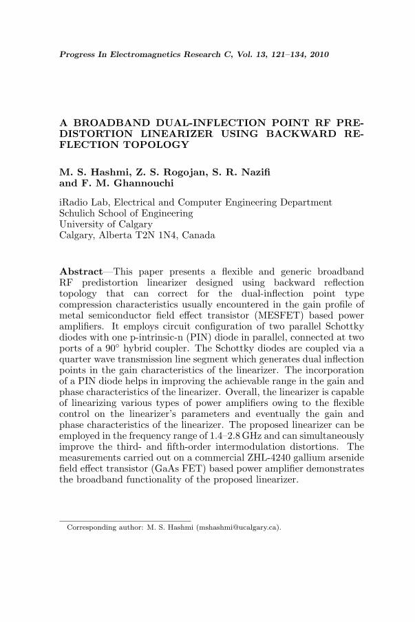
The block diagram of the proposed Linearizer is shown in Fig. 1(a). Itconsists of two similar circuit configurations, Fig. 1(b), at the secondand third ports of a quadrature hybrid. The configuration in Fig. 1(b)comprises of two parallel Schottky diodes, D1 and D2, and a PINdiode, D3. This configuration is substantially altered version of theone reported in [19].
The variable bias points, Vd1 and Vd2, of the diodes D1 andD2 generate the desired nonlinear distortions in the gain and phasecharacteristics of this linearizer. The bias points of D1 and D2 are thesuperposition of the DC static biases from the supply voltages, Vcc1
and Vcc2, and the rectified DC bias voltages resulting from the inputRF signal. This allows the control of nonlinear characteristics of thislinearizer by altering either the input RF signal or the supply voltages.The PIN diode, D3, primarily works as a dynamic resistance, regulatedby its bias voltage Vd3, and is used to achieve better dynamic controlin the gain and phase characteristics of the linearizer. All the diodesare biased via separate feed resistances Rb1, Rb2 and Rb3 respectively.This ensures that the diodes can be biased independent of each otherand at different bias levels thus providing the higher degree of freedomin achieving any phase and gain characteristic. The λ/4 transmissionline provides the dual-inflection points in the gain characteristic of thelinearizer.
The Fig. 1(a) can be analysed to determine the relationship
1
23
90
HybridCoupler
ο
4 1( )b f a=
1a
3a 3b2b2a
IN OUTISO
LL
Γ
3D2D1
1bR
2bR
3bR
1CV
Γ
1dV 2dV 3dV
D
(a) (b)
1
2CV 3CV
cc cλ/4
Figure 1. (a) The block diagram of the linearizer (left). (b) Schematicdiagram of the circuit configuration L (right).
124 Hashmi et al.
between the input signal, a1, and the output signal, b4. Thisdependence of b4 on a1 is regulated by the reflection coefficient, Γ, ofthe circuit configuration (L), Fig. 1(b), at the two ports of the hybridcoupler. The reflection coefficient, Γ, can be written as:
Γ = |Γ|∠ϕ = s11 (1)
where |Γ| is the magnitude of the reflection coefficient, ϕ is the phaseof the associated reflection coefficient, and the s-parameter is for thecircuit configuration, Fig. 1(b), given by:
s11 =− [
Z20 · (Y1Y2 + Y1R3) + Z0 · (−Y1 + Y2 + R3)
]
Z20 · (Y1Y2 + Y1R3) + Z0 · (Y1 + Y2 + R3) + 2
(2)
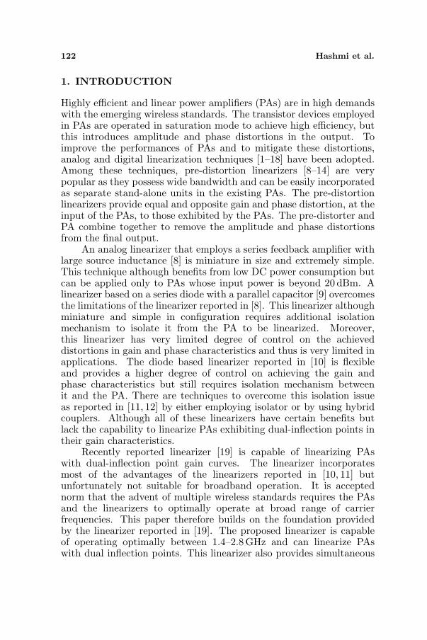
In the above equation Y1 and Y2 are the admittances of theSchottky diodes, D1 and D2 respectively, and R3 is the total resistanceof the PIN diode, D3. The admittances Y1 and Y2 and can be derivedby analyzing the equivalent circuit in Fig. 2(b) as explained below:
2D1D
/4λc
1bR 2bR
1CV 2CV
1dV 2dV
R1Cj1V1 V2
I1 I2
R2Cj2
4
(a) (b)
Figure 2. (a) The two Schottky diodes coupled by a quarter wave line(left). (b) The equivalent circuit of the Schottky diode configuration(right).
The total resistance for each diode is R1 and R2, respectively:
R1 =Rd1 ×Rb1
Rd1 + Rb1(3)
R2 =Rd2 ×Rb2
Rd2 + Rb2(4)
where, Rd1 and Rd2 are the dynamic resistances of the Schottky diodes
Progress In Electromagnetics Research C, Vol. 13, 2010 125
D1 and D2 respectively. Then the admittances Y1 and Y2 are given by:
Y1 =1 + jω · Cj1R1
R1(5)
Y2 =1 + jω · Cj2R2
R2(6)
where Cj1 and Cj2 are the junction capacitances of the Schottky diodesD1 and D2 respectively.
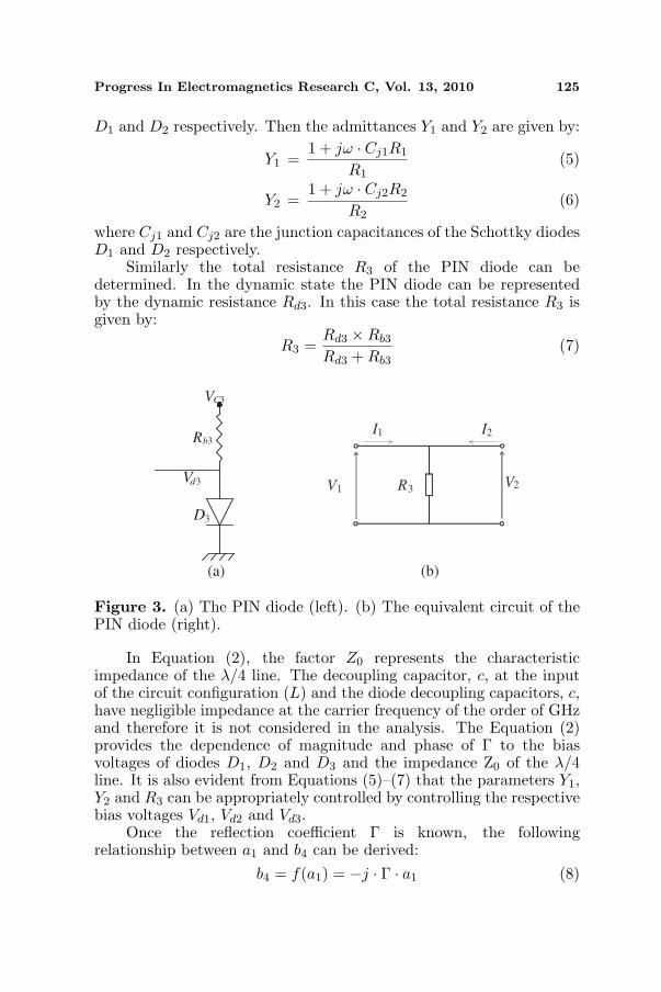
Similarly the total resistance R3 of the PIN diode can bedetermined. In the dynamic state the PIN diode can be representedby the dynamic resistance Rd3. In this case the total resistance R3 isgiven by:
R3 =Rd3 ×Rb3
Rd3 + Rb3(7)
3D
C3V
3dVR3V1
V2
I1 I2
(a)
3bR
(b)
Figure 3. (a) The PIN diode (left). (b) The equivalent circuit of thePIN diode (right).
In Equation (2), the factor Z0 represents the characteristicimpedance of the λ/4 line. The decoupling capacitor, c, at the inputof the circuit configuration (L) and the diode decoupling capacitors, c,have negligible impedance at the carrier frequency of the order of GHzand therefore it is not considered in the analysis. The Equation (2)provides the dependence of magnitude and phase of Γ to the biasvoltages of diodes D1, D2 and D3 and the impedance Z0 of the λ/4line. It is also evident from Equations (5)–(7) that the parameters Y1,Y2 and R3 can be appropriately controlled by controlling the respectivebias voltages Vd1, Vd2 and Vd3.
Once the reflection coefficient Γ is known, the followingrelationship between a1 and b4 can be derived:
b4 = f(a1) = −j · Γ · a1 (8)
126 Hashmi et al.
As |a1|2 = PIN and |b4|2 = POUT , the Equation (8) can be usedto determine the relationship for the output power versus input powerfor the linearizer:
POUT = |Γ|2 PIN (9)
Thus it is evident from Equation (9) that the term |Γ|2 regulatesthe gain and phase characteristics of the linearizer. It is also evidentfrom Equations (1)–(2) that the gain and phase of the reflectioncoefficient, Γ, can be controlled by altering the admittance Y1 andY2 of the Schottky diodes, dynamic resistance R3 of the PIN diodeand the impedance Z0 of the quarter wave transmission line couplingthe Schottky diodes D1 and D2.
The prototype for this proposed linearizer was built on a RT/5880duroid substrate with a dielectric constant of 2.2 and thickness of0.508mm. The chosen PIN and Schottky diodes were from Agilent withmodels HMPP-3890 and HSMS-2820 respectively, while the chosen90 hybrid coupler is from Anaren. In the current investigation, the1 W GaAs FET amplifier was used for the purpose of linearization.Therefore simulations were carried out on the linearizer to determinethe values of the design parameters identified in Equation (2) such thatthe predistorter will be customized and aligned with the amplifier
For the present case, the optimal value of the impedance of thequarter wave length transmission line section comes out to be 45Ω.The values for the bias feed resistances Rb1, Rb2 and Rb3 comes equalto 1 kΩ. It will be demonstrated in the next section that proper controlof bias voltage for D1, D2 and D3 generates the desired phase and gaincharacteristics.
3. EVALUATION OF THE LINEARIZER
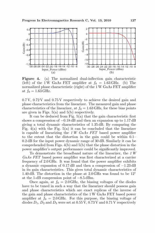
To evaluate the performance of the designed linearizer, first a 1 WGaAs FET amplifier was selected. The normalized gain and phasecharacteristic of the amplifier, at carrier frequency f0 of 1.63 GHz, isshown in Figs. 4(a) and 4(b) respectively. It is evident from 4(a) thatthe gain characteristic exhibits a dynamic expansion of 0.16 dB andthen a compression of −1.18 dB for the input power dynamic range of30 dB. This gives a total dynamic characteristic of 1.34 dB. It can alsobe deduced from Fig. 4(b) that the chosen 1W GaAs FET amplifierexhibits phase distortion of −10 at the input 1 dB compression pointof −8.5 dBm.
In principle, the linearizer should possess gain and phasecharacteristics which are exact replicas of the inverse of the gain andphase characteristics given in Figs. 4(a) and 4(b) respectively. Forthis purpose, the biasing voltage of diodes D1, D2 and D3 were set at
Progress In Electromagnetics Research C, Vol. 13, 2010 127
Figure 4. (a) The normalized dual-inflection gain characteristic(left) of the 1 W GaAs FET amplifier at f0 = 1.63GHz. (b) Thenormalized phase characteristic (right) of the 1 W GaAs FET amplifierat f0 = 1.63GHz.
0.7V, 0.72V and 0.75 V respectively to achieve the desired gain andphase characteristics from the linearizer. The measured gain and phasecharacteristics of the linearizer, at f0 = 1.63GHz, for these bias pointsare given in Figs. 5(a) and 5(b) respectively.
It can be deduced from Fig. 5(a) that the gain characteristic firstshows a compression of −0.18 dB and then an expansion up to 1.17 dBgiving a total dynamic characteristics of 1.35 dB. By comparing theFig. 4(a) with the Fig. 5(a) it can be concluded that the linearizeris capable of linearizing the 1W GaAs FET based power amplifierto the extent that the distortion in the gain could be within 0.1–0.2 dB for the input power dynamic range of 30 dB. Similarly it can becomprehended from Figs. 4(b) and 5(b) that the phase distortion in thepower amplifier’s output performance could be significantly improved.
To demonstrate the broadband nature of the linearizer, the 1WGaAs FET based power amplifier was first characterized at a carrierfrequency of 2.0 GHz. It was found that the power amplifier exhibitsa dynamic expansion of 0.17 dB and then a compression of −1.23 dBin its gain characteristics. This gives total dynamic characteristics of1.40 dB. The distortion in the phase at 2.0 GHz was found to be 12at the 1-dB compression point of −8.5 dBm.
Once again, at f0 = 2.0GHz, the biasing voltages of the diodeshave to be tuned in such a way that the linearizer should possess gainand phase characteristics which are exact replicas of the inverse ofthe gain and phase characteristics of the 1 W GaAs FET based poweramplifier at f0 = 2.0GHz. For this purpose, the biasing voltage ofdiodes D1, D2 and D3 were set at 0.55 V, 0.73 V and 0.71 V respectively
Figure 5. (a) The measured normalized gain characteristic (left)of the proposed linearizer at f0 = 1.63GHz. (b) The measurednormalized phase characteristic (right) of the linearizer at f0 =1.63GHz.
Figure 6. (a) The measured normalized gain characteristic (left) ofthe proposed linearizer at f0 = 2.0 GHz. (b) The measured normalizedphase characteristic (right) of the linearizer at f0 = 2.0 GHz.
to achieve the desired gain and phase characteristics from the linearizer.The measured gain and phase characteristics of the linearizer, atf0 = 2.0GHz, for these bias points are given in Figs. 6(a) and 6(b)respectively.
It can be seen in Fig. 6(a) that the gain characteristic first showsa compression of −0.19 dB and then an expansion up to 1.19 dB givinga total dynamic characteristics of 1.38 dB. This achieved dynamiccharacteristic in the gain of the linearizer is very close to the inverseof the gain characteristics of the 1W GaAs FET based PA. Thus itcan be concluded that the linearizer is capable of linearizing the 1W
Progress In Electromagnetics Research C, Vol. 13, 2010 129
GaAs FET based power amplifier at f0 = 2.0 GHz to the extent thatthe distortion in the gain could be around 0.1 dB for the input powerdynamic range of 30 dB. It is evident from Fig. 6(b) that the linearizergives a phase distortion of 13 at the 1-dB compression points.Therefore it can be comprehended that the phase distortion in thepower amplifier’s output performance can be significantly improved.
4. EXPERIMENTAL VALIDATION OF THELINEARIZER
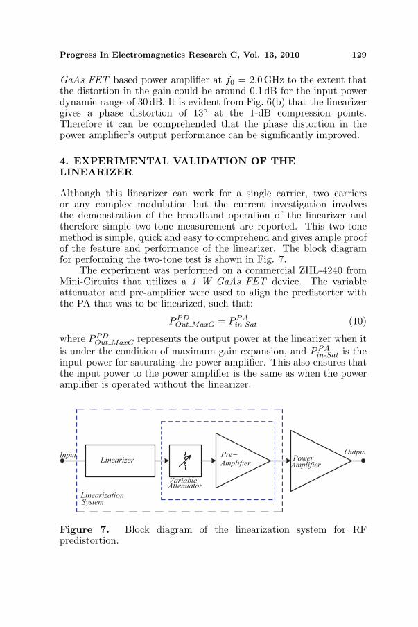
Although this linearizer can work for a single carrier, two carriersor any complex modulation but the current investigation involvesthe demonstration of the broadband operation of the linearizer andtherefore simple two-tone measurement are reported. This two-tonemethod is simple, quick and easy to comprehend and gives ample proofof the feature and performance of the linearizer. The block diagramfor performing the two-tone test is shown in Fig. 7.
The experiment was performed on a commercial ZHL-4240 fromMini-Circuits that utilizes a 1 W GaAs FET device. The variableattenuator and pre-amplifier were used to align the predistorter withthe PA that was to be linearized, such that:
PPDOut MaxG = PPA
in-Sat (10)
where PPDOut MaxG represents the output power at the linearizer when it
is under the condition of maximum gain expansion, and PPAin-Sat is the
input power for saturating the power amplifier. This also ensures thatthe input power to the power amplifier is the same as when the poweramplifier is operated without the linearizer.
OutputInput
VariableAttenuator
PreAmplifier
−
LinearizationSystem
PowerAmplifier
Linearizer
Figure 7. Block diagram of the linearization system for RFpredistortion.
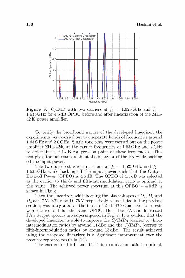
Figure 8. C/IMD with two carriers at f1 = 1.625 GHz and f2 =1.635GHz for 4.5 dB OPBO before and after linearization of the ZHL-4240 power amplifier.
To verify the broadband nature of the developed linearizer, theexperiments were carried out two separate bands of frequencies around1.63GHz and 2.0 GHz. Single tone tests were carried out on the poweramplifier ZHL-4240 at the carrier frequencies of 1.63 GHz and 2 GHzto determine the 1-dB compression point at these frequencies. Thistest gives the information about the behavior of the PA while backingoff the input power.
The two-tone test was carried out at f1 = 1.625GHz and f2 =1.635GHz while backing off the input power such that the OutputBack-off Power (OPBO) is 4.5 dB. The OPBO of 4.5 dB was selectedas the carrier to third- and fifth-intermodulation ratio is optimal atthis value. The achieved power spectrum at this OPBO = 4.5 dB isshown in Fig. 8.
Then the linearizer, while keeping the bias voltages of D1, D2 andD3 at 0.7 V, 0.72V and 0.75V respectively as identified in the previoussection, was integrated at the input of ZHL-4240 and two tone testswere carried out for the same OPBO. Both the PA and linearizedPA’s output spectra are superimposed in Fig. 8. It is evident that thedeveloped linearizer is able to improve the C/IMD3 (carrier to third-intermodulation ratio) by around 11 dBc and the C/IMD5 (carrier tofifth-intermodulation ratio) by around 13 dBc. The result achievedusing the proposed linearizer is a significant improvement over therecently reported result in [19].
The carrier to third- and fifth-intermodulation ratio is optimal,
Progress In Electromagnetics Research C, Vol. 13, 2010 131
around frequency of 2 GHz, when the OPBO of 5 dB was achieved.Therefore the two-tone test at f1 = 1.995GHz and f2 = 2.005GHzwas carried out while backing off the input power such that the OutputBack-off Power (OPBO) is 5 dB. The achieved power spectrum, whilemeasurement is carried out only on the ZHL-4240 alone, is shown inFig. 8. Then the two-tone test was once again carried out while thelinearizer, with the bias voltages of D1, D2 and D3 were set at 0.55 V,0.73 V and 0.71 V respectively as identified in the previous section, isplaced at the input of ZHL-4240. Both the PA and linearized PA’soutput spectra are superimposed in Fig. 9. It is evident that thedeveloped linearizer is able to improve the C/IMD3 (carrier to third-intermodulation ratio) by around 10 dBc and the C/IMD5 (carrier tofifth-intermodulation ratio) by around 13 dBc.
The achieved result at the frequency band around 2 GHz is alsosimilar to the results obtained at frequency band around 1.63 GHz.Thus it can be concluded that the proposed linearizer is capable ofoperating properly at a wide range of frequency of interest. Thelimitation on frequency ranges from 1.4GHz to 2.8 GHz is due tothe components used in the design of the linearizer. This linearizertopology could be extended to work in other frequency band bychanging the components.
Figure 9. C/IMD with two carriers at f1 = 1.995 GHz and f2 =2.005GHz for 5 dB OPBO before and after linearization of the ZHL-4240 power amplifier.
132 Hashmi et al.
5. CONCLUSION
A new broadband, miniature, dual-inflection point, analog, backwardreflection based predistortion linearizer using parallel diode configura-tion, coupled with a quarter wave transmission line section, has beenpresented. The linearizer possesses four degrees of control to achievethe desired output characteristics through i) control of the bias volt-age of the Schottky diode D1, ii) control of the bias voltage of theSchottky diode D2, iii) control of the bias voltage of the PIN diodeD3, and iv) control of the impedance of the quarter wave transmissionline section. To verify the broadband feature of the linearizer, a 1 WGaAs FET amplifier was taken as a case study; and, the proposedlinearizer’s characteristic was controlled by the diode bias voltages soas to achieve a characteristic curves which are inverse to those of theGaAs FET PA. Then the two-tone tests were carried out at frequencybands around 1.63 GHz and 2.0GHz. The results clearly show a si-multaneous reduction of third- and fifth-order distortion in both theselected frequency bands. These measurements on a commercial poweramplifier, ZHL-4240 based on a 1W GaAs FET device, demonstratedthe successful broadband operation of the proposed linearizer.
ACKNOWLEDGMENT
The authors would like to acknowledge the financial support fromAlberta Informatics Circle of Research Excellence (iCORE), theNatural Sciences and Engineering Research Council of Canada(NSERC) and Canada Research Chair (CRC) program. The authorsare also thankful to the staffs of the iRadio Lab for the technicalassistance.
REFERENCES
1. Helaoui, M. and F. M. Ghannouchi, “Linearization of power am-plifiers using the reverse mm-linc technique,” IEEE Transactionson Circuits and Systems II: Express Briefs, Vol. 57, No. 1, 6–10,January 2010.
2. Hammi, O., S. Carichner, B. Vassilakis, and F. M. Ghannouchi,“Synergetic crest factor reduction and baseband digital predistor-tion for adaptive 3G Doherty power amplifier linearizer design,”IEEE Transactions on Microwave Theory and Techniques, Vol. 56,No. 11, 2602–2608, November 2008.
3. Kim, J., Y. Y. Woo, J. Cha, S. Hong, I. L. Kim, J. Moon,J. Kim, and B. Kim, “Analog predistortion of high power amplifier
Progress In Electromagnetics Research C, Vol. 13, 2010 133
using novel low memory matching topology,” Journal of the KoreaElectromagnetic Engineering Society, Vol. 7, No. 4, 146–153,December 2007.
4. Kursu, O., M. Riikola, J. Aikio, and T. Rahkonen, “Polynomial2.1GHz RF Predistorter with envelope injection output,” SpringerAnalog Integrated Circuit and Signal Processing, Vol. 50, No. 1,13–20, January 2007.
5. Teikari, I., J. Vankka, and K. Halonen, “Digitally controlledRF predistortion with digital predictor for feedforward delaycompensation,” IEEE MTT-S Int. Microwave Symp. Digest,2043–2046, Long Beach, CA, May 2005.
6. Zhao, G., F. M. Ghannouchi, F. Beauregard, and A. B. Kouki,“Digital implementations of adaptive feedforward amplifierlinearization techniques,” IEEE MTT-S International MicrowaveSymposium, Vol. 2, No. 2, 543–546, June 1996.
7. Eid, E. E. and F. M. Ghannouchi, “Adaptive nulling loop controlfor 1.7-GHz feedforward linearization systems,” IEEE Trans.Microw. Theory Tech., Vol. 45, No. 1, 83–86, January 1997.
8. Nakayama, M., K. Mori, K. Yamauchi, Y. Itoh, and T. Takagi, “Anovel amplitude and phase linearizing technique for microwavepower amplifiers,” IEEE MTT-S Int. Microwave Symp. Digest,1451–1454, Orlando, FL, May 1995.
9. Yamauchi, K., K. Mori, M. Nakayama, Y. Itoh, Y. Mitsui, andO. Ishida, “A novel series diode linearizer for mobile radio poweramplifiers,” IEEE MTT-S International Microwave SymposiumDigest, 831–834, 1996.
10. Yamauchi, K., K. Mori, M. Nakayama, Y. Mitsui, and T. Takagi,“A microwave miniaturized linearizer using a parallel diode witha bias feed resistance,” IEEE Trans. on Microw. Theory Tech.,Vol. 45, No. 12, 2431–2435, December 1997.
11. Park, C.-W., F. Beauregard, G. Carangelo, and F. M. Ghan-nouchi, “An independently controllable AM/AM and AM/PMpredistortion linearizer for CDMA2000 multi-carrier applica-tions,” IEEE MTT-S Int. Microwave Symp. Digest, 53–56,Phoenix, May 2001.
12. Ghannouchi, F. M. and J. S. Cardinal, “A new adaptive doubleenvelope feedback linearizer for mobile radio power amplifiers,”IEEE MTT-S Int. Microwave Symp. Digest, 573–576, San Diego,May 1994.
13. Gupta, N., A. Tombak, and A. Mortazawi, “A predistortionlinearizer using a tunable resonator,” IEEE Microw. WirelessCompon. Lett., Vol. 14, No. 9, 431–433, September 2004.
134 Hashmi et al.
14. Katz, A., “Linearization: Reducing distortion in poweramplifiers,” IEEE Microwave, Vol. 2, 37–49, December 2001.
15. Ma, H. and Q. Feng, “An improved design of feed-forward poweramplifier,” PIERS Online, Vol. 3, No. 4, 363–367, 2007.
16. Hau, G., T. B. Nishimura, and N. Iwata, “A highly efficientlinearized wide-band CDMA handset power amplifier basedon predistortion under various bias conditions,” IEEE Trans.Microw. Theory Tech., Vol. 49, 1194–1200, June 2001.
17. Suematsu, N., T. Takeda, A. Lida, and S. Urasaki, “Apredistortion type equipath linearizer in Ku-band,” Proc. 3rd AsiaPacific Microwave Conf., 1077–1088, Tokyo, September 1990.
18. Boulejfen, N., A. Harguem, and F. M. Ghannouchi, “New closed-form expressions for the prediction of multitone intermodulationdistortion in fifth-order nonlinear RF circuits/systems,” IEEETrans. Microw. Theory Tech., Vol. 52, No. 1, 121–132, January2004.
19. Hashmi, M. S., Z. S. Rogojan, and F. M. Ghannouchi, “A flexibledual-inflection point RF predistortion linearizer for microwavepower amplifiers,” Progress In Electromagnetics Research C,Vol. 13, 1–18, 2010.


![Train-to-Ground Wireless Broadband Communication for … · Train-to-Ground Wireless Broadband Communication for ... Distortion effects like the Doppler effect [2] ... The train will](https://static.documents.pub/doc/80x56/5afa9e4a7f8b9a5f588fb8a4/train-to-ground-wireless-broadband-communication-for-wireless-broadband-communication.jpg)


