Page 1
A COGNITIVE PHASED ARRAY USING SMART PHONE CONTROL
A Thesis
by
JEFFREY SCOTT JENSEN
Submitted to the Office of Graduate Studies of
Texas A&M University
in partial fulfillment of the requirements for the degree of
MASTER OF SCIENCE
May 2012
Major Subject: Electrical Engineering
Page 2
A Cognitive Phased Array Using Smart Phone Control
Copyright 2012 Jeffrey Scott Jensen
Page 3
A COGNITIVE PHASED ARRAY USING SMART PHONE CONTROL
A Thesis
by
JEFFREY SCOTT JENSEN
Submitted to the Office of Graduate Studies of
Texas A&M University
in partial fulfillment of the requirements for the degree of
MASTER OF SCIENCE
Approved by:
Chair of Committee, Gregory H. Huff
Committee Members, Jean-Francois Chamberland
Harry A. Hogan
Henry D. Pfister
Head of Department, Costas Georghiades
May 2012
Major Subject: Electrical Engineering
Page 4
iii
ABSTRACT
A Cognitive Phased Array Using Smart Phone Control. (May 2012)
Jeffrey Scott Jensen, B.S., Texas A&M University
Chair of Advisory Committee: Dr. Gregory H. Huff
Cognitive radio networks require the use of computational resources to reconfigure
transmit/receive parameters to improve communication quality of service or efficiency.
Recent emergence of smart phones has made these resources more accessible and
mobile, combining sensors, geolocation, memory and processing power into a single
device. Thus, this work examines an integration of a smart phone into a complex radio
network that controls the beam direction of a phased array using a conventional method,
but utilizes the phone’s internal sensors as an enhancement to generate beam direction
information, Bluetooth channel to relay information to control circuitry, and Global
Position System (GPS) to track an object in motion.
The research and experiments clearly demonstrate smart phone’s ability to utilize
internal sensors to generate information used to control beam direction from a phased
array. Computational algorithms in a network of microcontrollers map this information
into a DC bias voltage which is applied to individual phase shifters connected to
individual array elements.
Page 5
iv
To test algorithms and control theory, a 4 by 4 microstrip patch array is designed and
fabricated to operate at a frequency of 2.4 GHz. Simulations and tests of the array
provide successful antenna design results with satisfactory design parameters. Smart
phone control circuitry is designed and tested with the array. Anechoic test results yield
successful beam steering capability scanning 90 degrees at 15 degree intervals with 98%
accuracy in all cases. In addition, the system achieves successful beam steering operable
over a bandwidth of 100 MHz around resonance. Furthermore, these results
demonstarate the capability of the smart phone controlled system to be used in testing
further array formations to achieve beam steering in 3-Dimensional space. It is further
noted that the system extends capabilities of integrating other control methods which use
the smart phone to process information.
Page 6
v
DEDICATION
This thesis is dedicated to my wife and parents.
Page 7
vi
ACKNOWLEDGEMENTS
I would like to thank my committee chair, Dr. Huff, for his help and experience
throughout this project. I would also like to thank my committee members, Dr.
Chamberland, Dr. Pfister, Dr. Hogan, for their guidance and support throughout the
course of this research.
In addition, I would like to thank my wife whose support and love has helped me
through hard work and difficult times. My success thrived with each day of her support.
In conjunction, I would also like to thank my parents who taught me that you always
need to love what you do and hard work always pays off. Thank you.
Page 8
vii
NOMENCLATURE
GPS Global Positioning System
ROM Read Only Memory
RAM Random Access Memory
OS Operating System
PHY Physical Layer
MAC Media Access Control
QOS Quality of Service
TCP Transport Control Protocol
UDP User Datagram Protocol
SSH Secure Shell
SMTP Simple Mail Transfer Protocol
SDA Serial Data Line
SCL Serial Clock Line
SPI Serial Peripheral Interface
I2C/I2C Inter-Integrated Circuit
ISM Industrial, Scientific, and Medical Radio Bands
VSWR Voltage Standing Wave Ratio
Page 9
viii
TABLE OF CONTENTS
Page
ABSTRACT .............................................................................................................. iii
DEDICATION .......................................................................................................... v
ACKNOWLEDGEMENTS ...................................................................................... vi
NOMENCLATURE .................................................................................................. vii
TABLE OF CONTENTS .......................................................................................... viii
LIST OF FIGURES ................................................................................................... x
LIST OF TABLES .................................................................................................... xv
CHAPTER
I INTRODUCTION ................................................................................ 1
II SURVEY .............................................................................................. 4
III BACKGROUND .................................................................................. 7
3.1 Array theory ............................................................................. 7
3.2 Control theory .......................................................................... 21
3.3 Control circuitry ....................................................................... 27
3.4 Communications ...................................................................... 34
IV SYSTEM DESIGN .............................................................................. 48
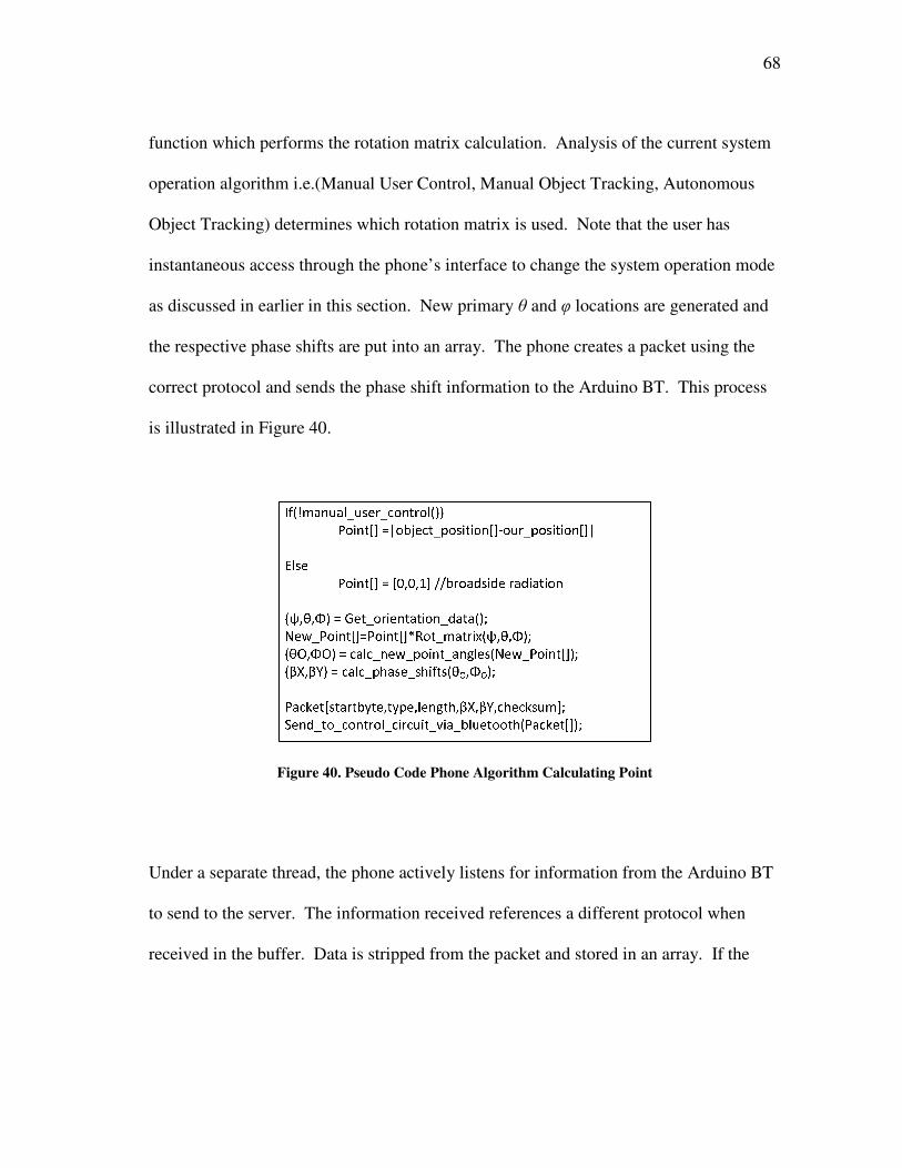
4.1 Array design ............................................................................. 48
4.2 Control design .......................................................................... 56
4.3 Circuit design ........................................................................... 67
4.4 Communications design ........................................................... 79
4.5 Phone and server display design .............................................. 82
Page 10
ix
CHAPTER Page
V COMPLETED DESIGN AND RESULTS ........................................... 86
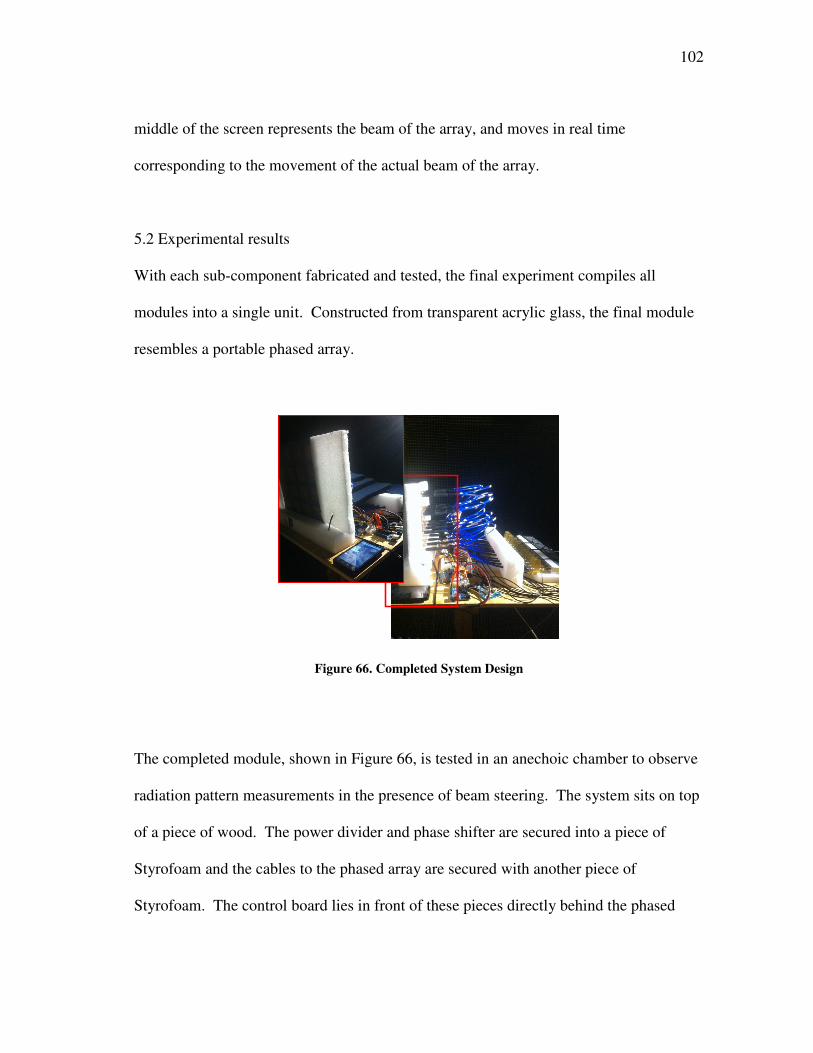
5.1 Completed design .................................................................... 86
5.2 Experimental results ................................................................ 102
VI CONCLUSIONS AND FUTURE WORK .......................................... 113
6.1 Summary .................................................................................. 113
6.2 Future work .............................................................................. 115
REFERENCES .......................................................................................................... 117
APPENDIX A SMARTPHONE CODE ................................................................... 120
APPENDIX B ARDUINO BT CODE ...................................................................... 132
APPENDIX C ARDUINO SLAVE 1 CODE ........................................................... 133
APPENDIX D ARDUINO SLAVE 2 CODE ........................................................... 140
APPENDIX E SERVER DISPLAY CODE .............................................................. 147
VITA ......................................................................................................................... 153
Page 11
x
LIST OF FIGURES
Page
Figure 1 Linear Microstrip Patch Array .................................................................. 7
Figure 2 Planar 4x4 Microstrip Patch Array ............................................................ 9
Figure 3 Microstip Patch with Design Parameters .................................................. 12
Figure 4 Wilkonson Power Divider Schematic ....................................................... 14
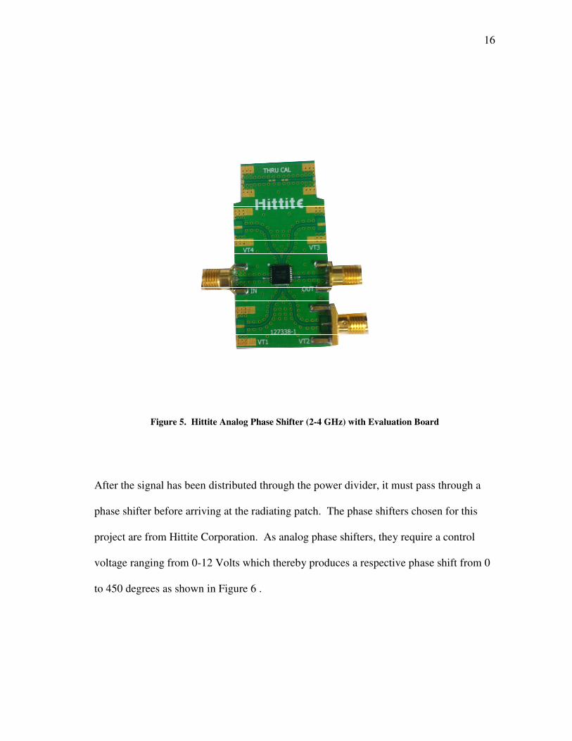
Figure 5 . Hittite Analog Phase Shifter (2-4 GHz) with Evaluation Board ........... 16
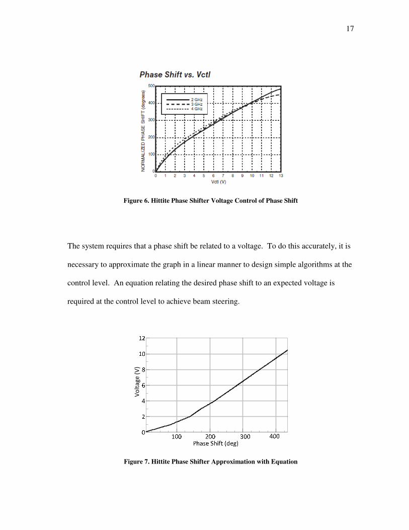
Figure 6 Hittite Phase Shifter Voltage Control of Phase Shift ............................... 17
Figure 7 Hittite Phase Shifter Approximation with Equation ................................. 17
Figure 8 Point in Cartesian Coordinates .................................................................. 19
Figure 9 Euler Angles to Construct Rotation Matrix .............................................. 20
Figure 10 Random Ordered List of Numbers ........................................................... 23
Figure 11 Open Loop Control from Input to Output ................................................ 25
Figure 12 Closed Loop Control from Input to Output ............................................. 26
Figure 13 Picture of HTC Evo Smart Phone ............................................................ 28
Figure 14 Smartphone and Respective Yaw, Pitch, and Roll .................................. 29
Figure 15 Arduino BT (Bluetooth Enabled) ............................................................ 30
Figure 16 Arduino Uno Microcontroller .................................................................. 31
Figure 17 Non-inverting Operational Amplifier Configuration ............................... 33
Figure 18 Linear Regulator with Pinout (Pin1 – Voltage Input, Pin2 – Ground,
Pin3 – Voltage Output) ........................................................................... 34
Figure 19 OSI Model and Data Flow ....................................................................... 36
Page 12
xi
Page
Figure 20 TCP Versus UDP ..................................................................................... 38
Figure 21 I2C Network with Master and Two Slaves .............................................. 40
Figure 22 I2C Timing Diagram ................................................................................ 41
Figure 23 SPI Network with Master and Two Slaves .............................................. 42
Figure 24 User with Internet Connection to Server .................................................. 47
Figure 25 VSWR for Single Patch Antenna ............................................................ 50
Figure 26 Input Impedance Single Patch Antenna .................................................. 51
Figure 27 Single Element Radiation Pattern ............................................................ 52
Figure 28 VSWR Infinite Array Simulation ............................................................ 53
Figure 29 Input Impedance Infinite Array ............................................................... 54
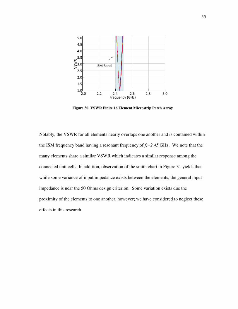
Figure 30 VSWR Finite 16 Element Microstrip Patch Array ................................... 55
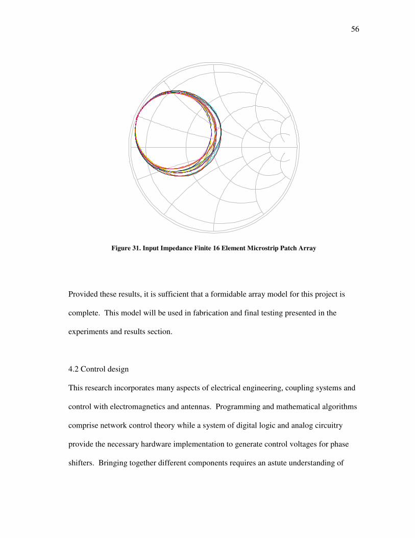
Figure 31 Input Impedance Finite 16 Element Microstrip Patch Array ................... 56
Figure 32 General Network Overview ..................................................................... 58
Figure 33 Network Overview with Physical Implementation .................................. 58
Figure 34 Manual Tracking Mode of Operation ...................................................... 59
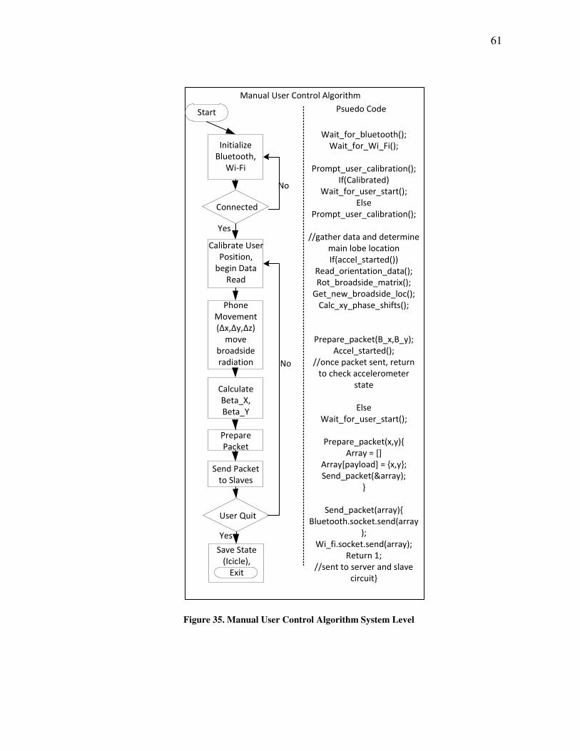
Figure 35 Manual User Control Algorithm System Level ...................................... 61
Figure 36 Manual Object Tracking Physical Representation .................................. 62
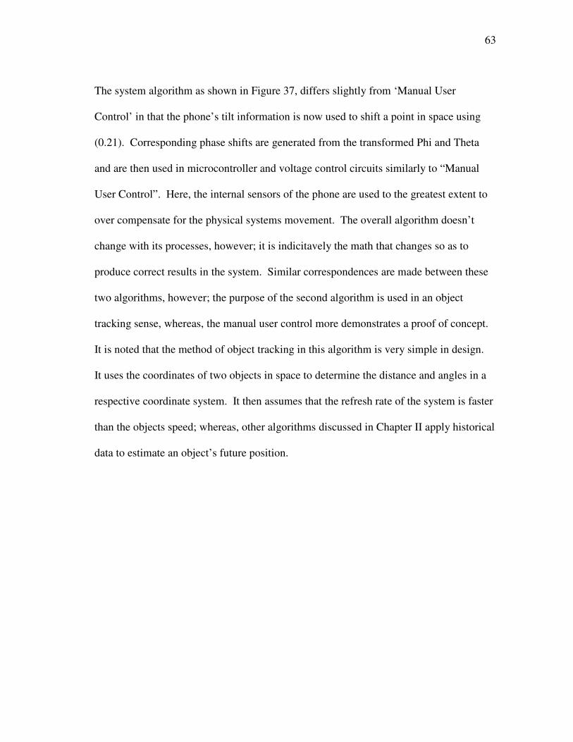
Figure 37 Manual Object Tracking Algorithm and Pseudo Code ........................... 64
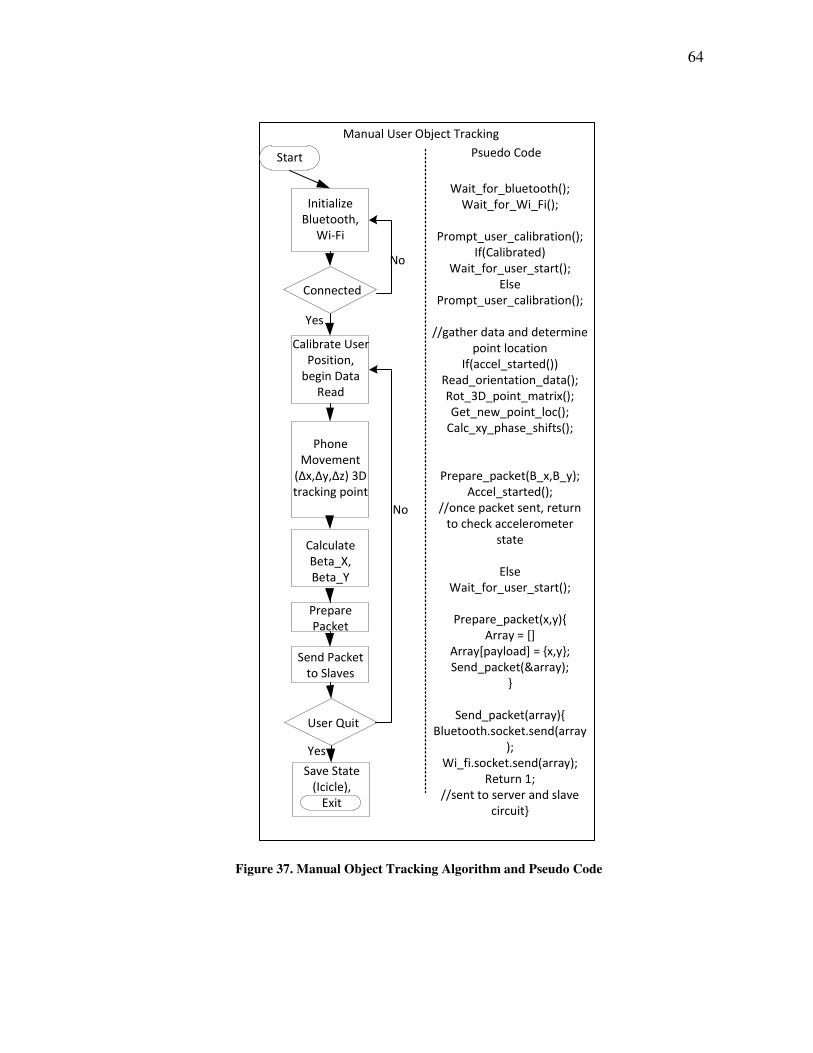
Figure 38 Autonomous Array Object Tracking ........................................................ 65
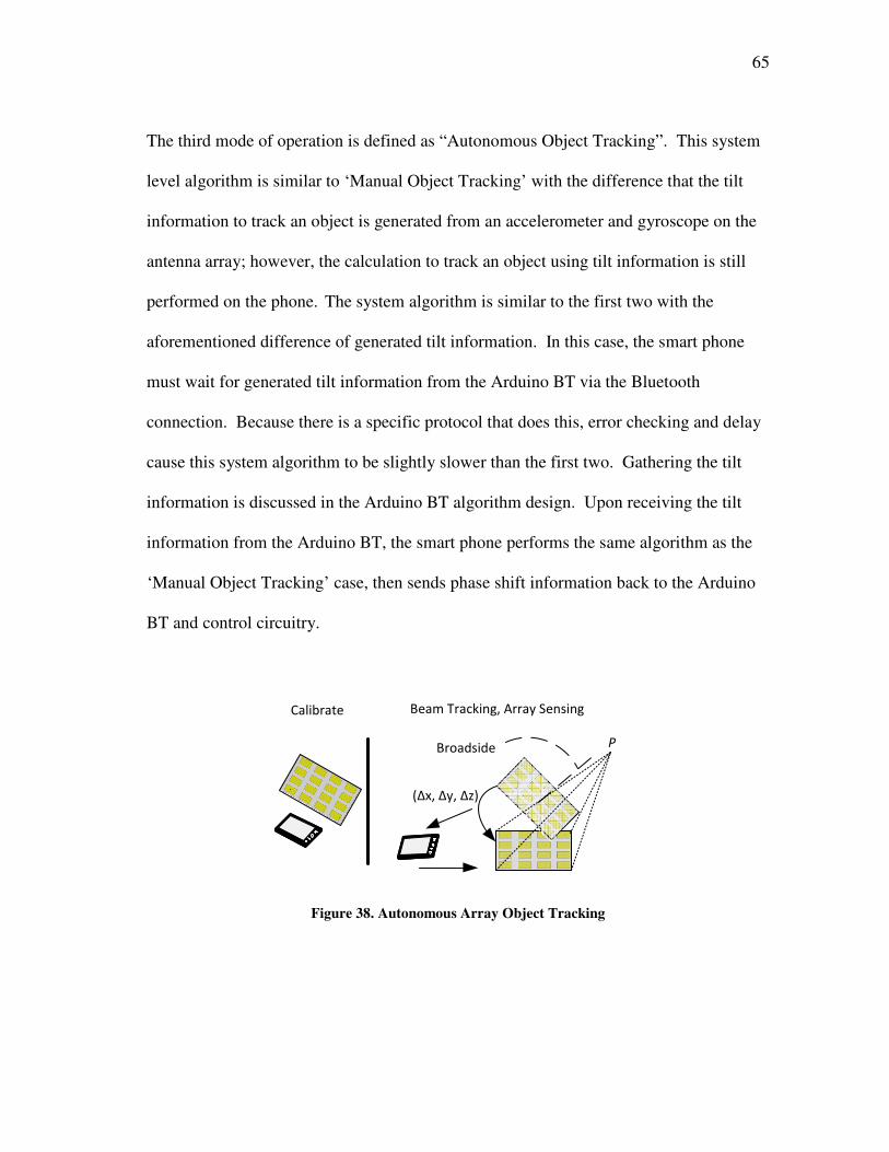
Figure 39 Autonomous Object Tracking Algorithm and Pseudo Code ................... 66
Figure 40 Pseudo Code Phone Algorithm Calculating Point ................................... 68
Page 13
xii
Page
Figure 41 Arduino Bluetooth Master Control Algorithm ........................................ 70
Figure 42 Main Beam Location in Various Cartesian Quadrants ............................ 71
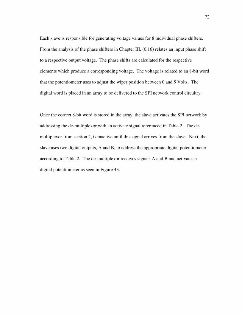
Figure 43 De-Multiplexor with Digital Potentiometer ............................................. 73
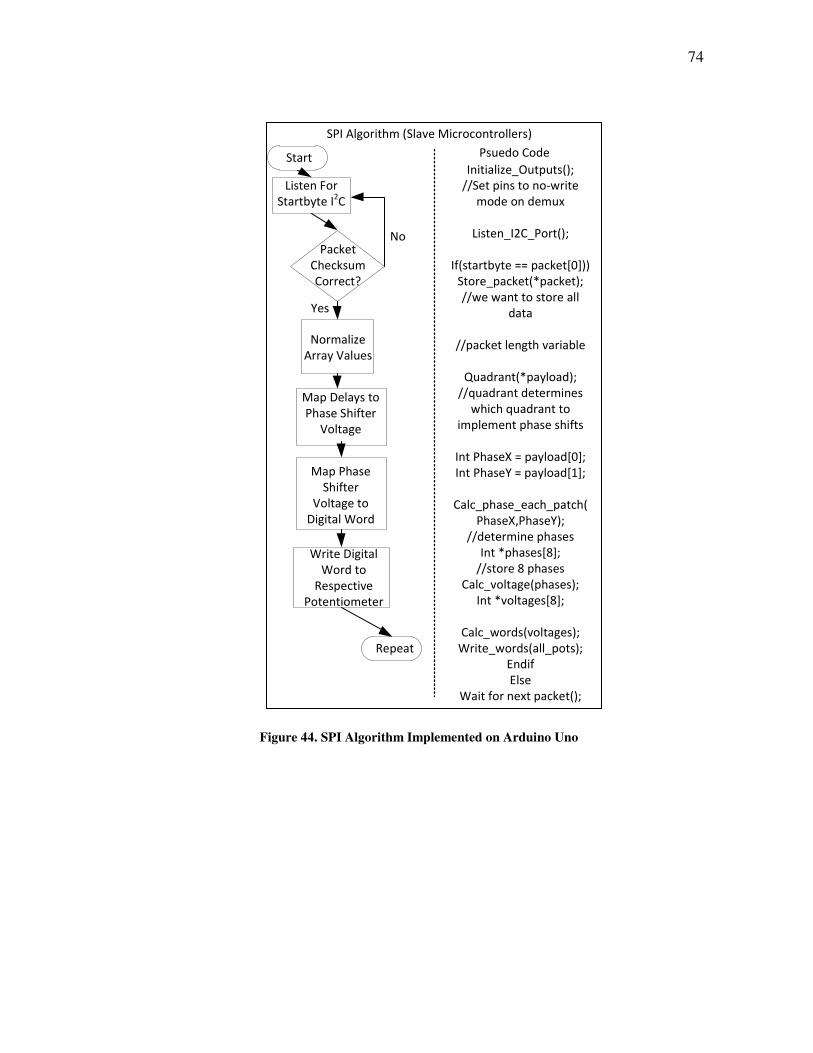
Figure 44 SPI Algorithm Implemented on Arduino Uno ......................................... 74
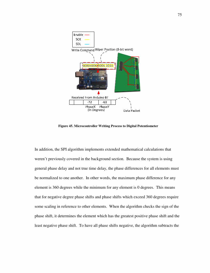
Figure 45 Microcontroller Writing Process to Digital Potentiometer ..................... 75
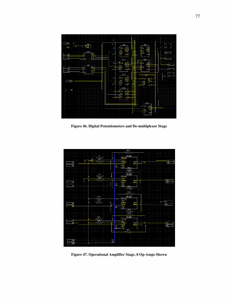
Figure 46 Digital Potentiometers and De-multiplexor Stage .................................. 77
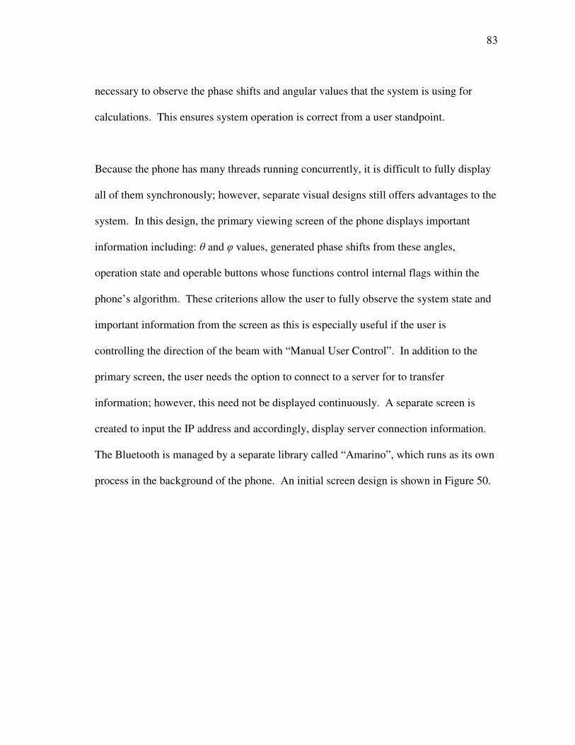
Figure 47 Operational Amplifier Stage, 8 Op-Amps Shown ................................... 77
Figure 48 Final PCB Design (Top Layer) Schematic (Left)
3-D Representation (Right) ..................................................................... 78
Figure 49 System Wide Protocol Packet Structure .................................................. 81
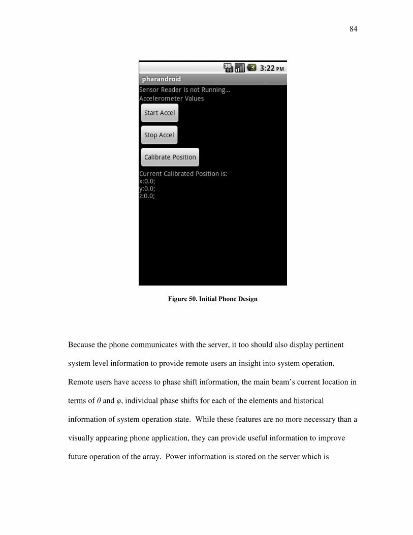
Figure 50 Initial Phone Design ................................................................................ 84
Figure 51 Initial Server Display Design ................................................................... 85
Figure 52 (Left) Fabricated Microstrip Patch Array (Right) Simulated
Microstrip Patch Array ........................................................................... 86
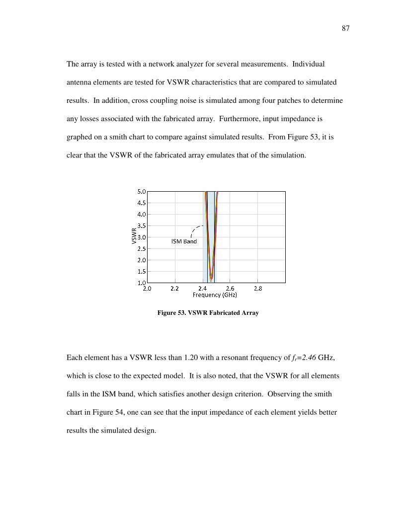
Figure 53 VSWR Fabricated Array .......................................................................... 87
Figure 54 Input Impedance Fabricated Array .......................................................... 88
Figure 55 S21 Measurements 4x4 Array ................................................................. 88
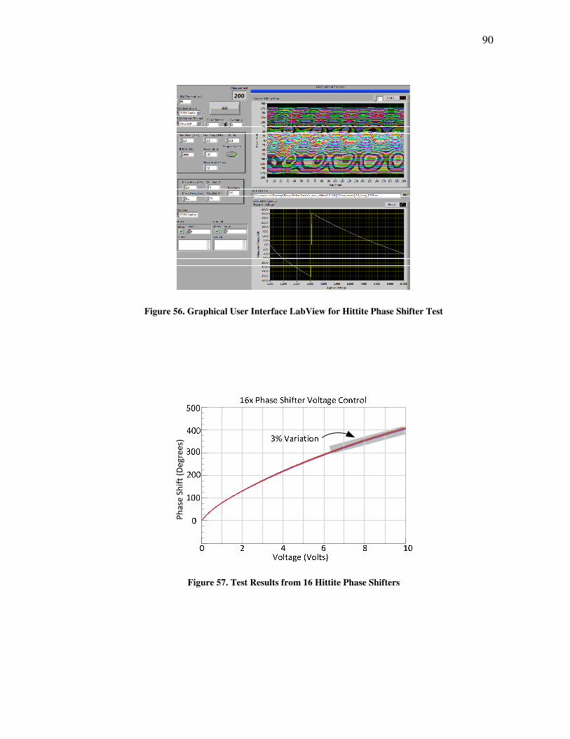
Figure 56 Graphical User Interface LabView for Hittite Phase Shifter Test ........... 90
Figure 57 Test Results from 16 Hittite Phase Shifters ............................................. 90
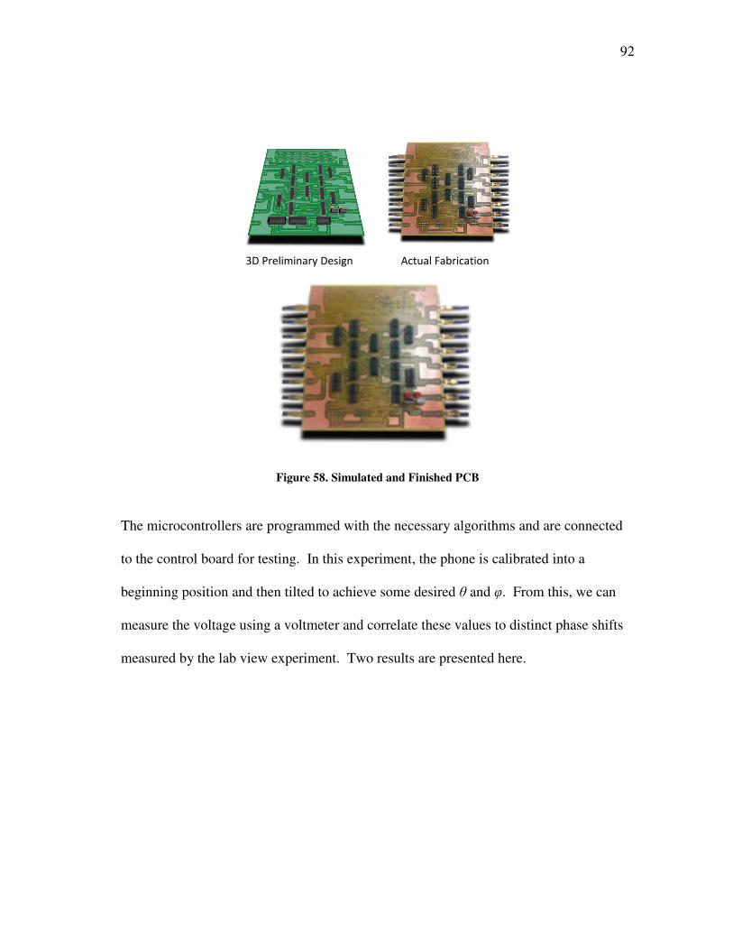
Figure 58 Simulated and Finished PCB .................................................................... 92
Page 14
xiii
Page
Figure 59 (Left) Polar Plot Experimental Results 45 Degree Cut Plane
(Right) Rectangular Plot 45 Degree Cut Plane ....................................... 94
Figure 60 (Left) Polar Experimental Plot 135 Degree Cut Plane (Right)
Rectangular Experimental Plot 135 Degree Cut Plane Electric Field ..... 96
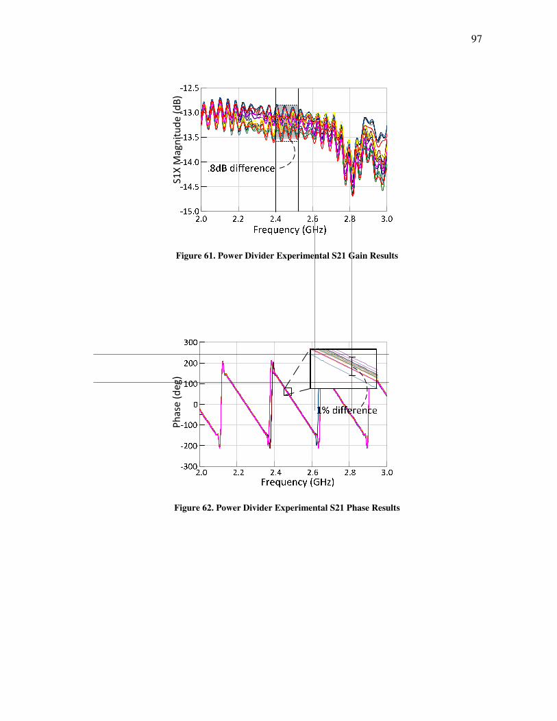
Figure 61 Power Divider Experimental S21 Gain Results ....................................... 97
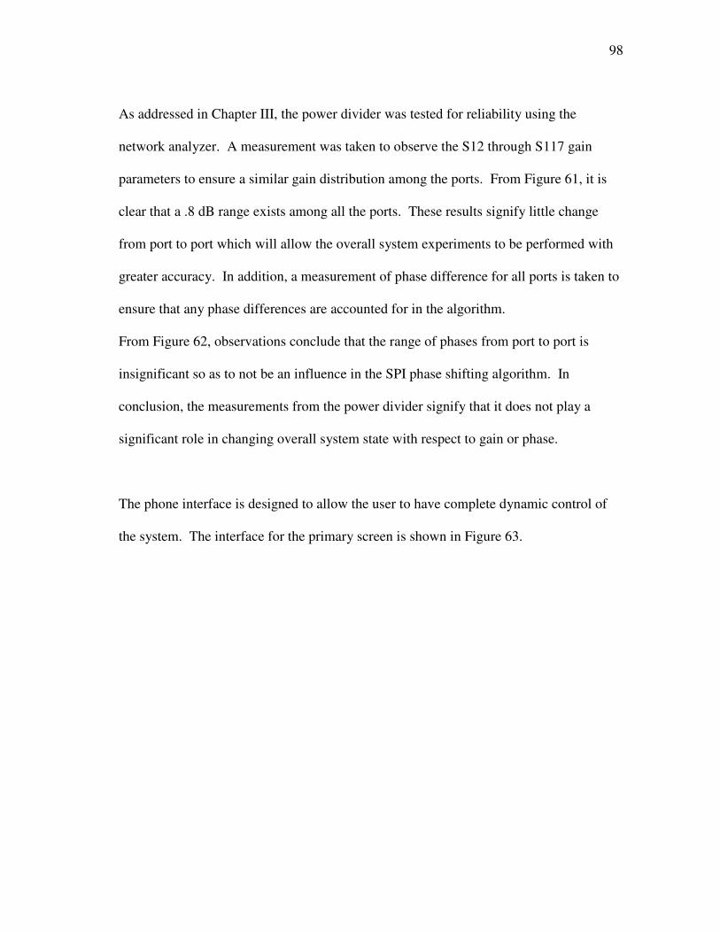
Figure 62 Power Divider Experimental S21 Phase Results ..................................... 97
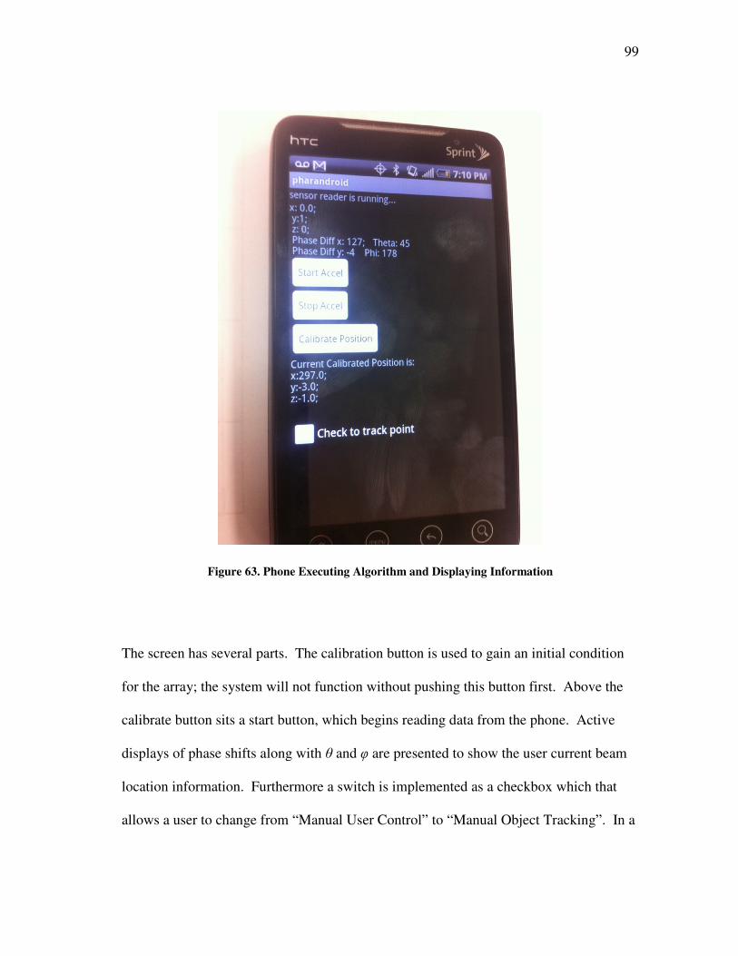
Figure 63 Phone Executing Algorithm and Displaying Information ........................ 99
Figure 64 Server Communication Page ................................................................... 100
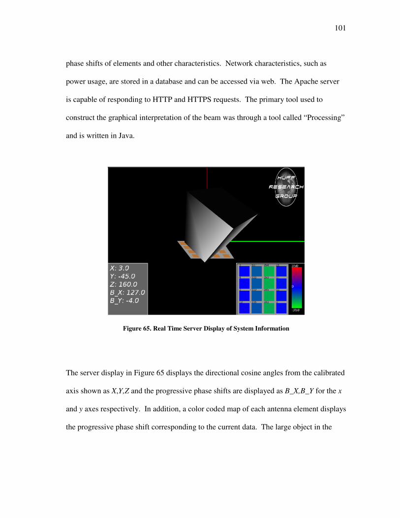
Figure 65 Real Time Server Display of System Information ................................... 100
Figure 66 Completed System Design ....................................................................... 102
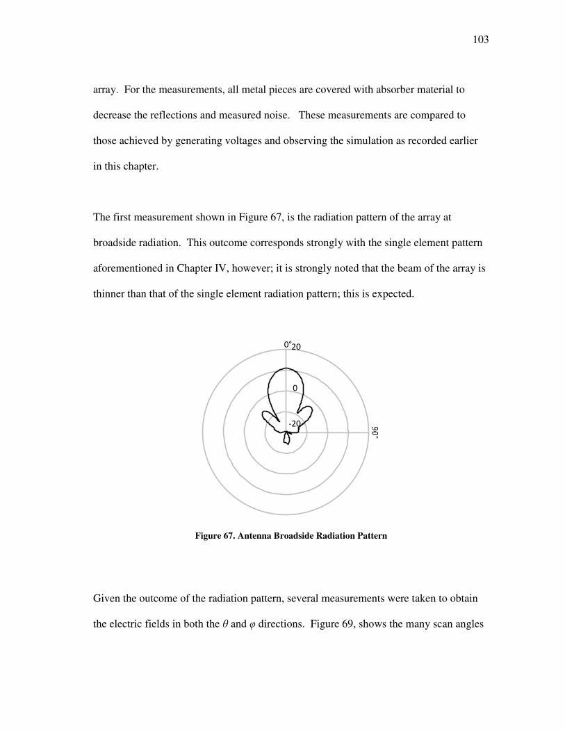
Figure 67 Antenna Broadside Radiation Pattern ...................................................... 103
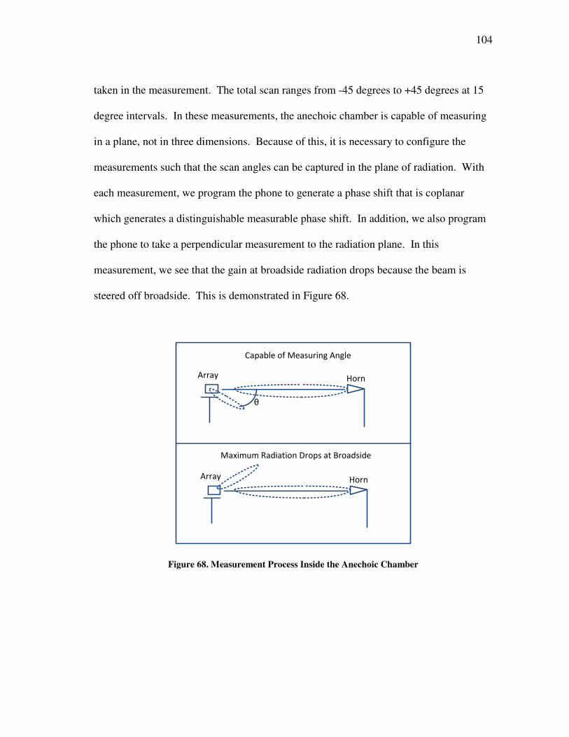
Figure 68 Measurement Process Inside the Anechoic Chamber ............................. 104
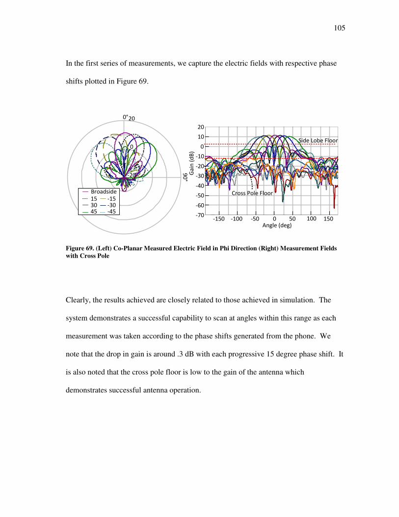
Figure 69 (Left) Co-Planar Measured Electric Field in Phi Direction (Right)
Measurement Fields with Cross Pole ...................................................... 105
Figure 70 (Left) Normal Measured Electric Field in Phi Direction (Right)
Measurement Fields with Cross Pole ...................................................... 106
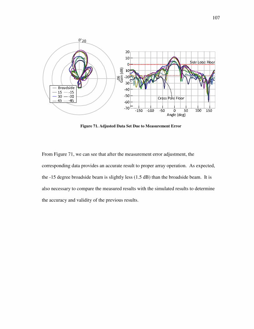
Figure 71 Adjusted Data Set Due to Measurement Error ......................................... 107
Figure 72 Simulated and Measured Comparison at +45 and -45 Degree Scan
Angles ..................................................................................................... 108
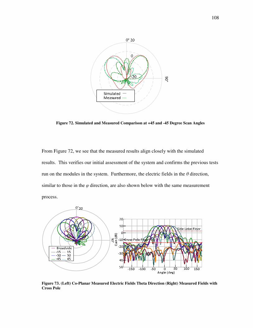
Figure 73 (Left) Co-Planar Measured Electric Fields Theta Direction (Right)
Measured Fields with Cross Pole ............................................................. 108
Page 15
xiv
Page
Figure 74 (Left) Normal Measured Electric Fields Theta Direction (Right)
Measured Fields with Cross Pole ............................................................. 109
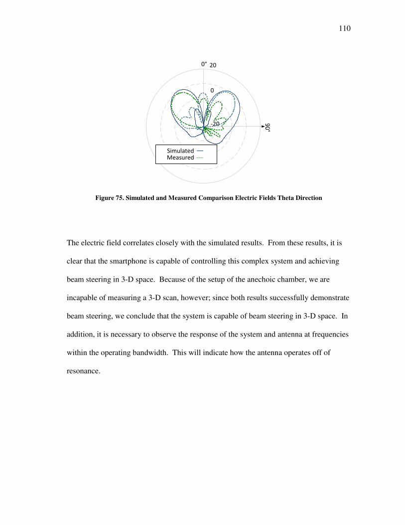
Figure 75 Simulated and Measured Comparison Electric Fields Theta Direction .. 110
Figure 76 Frequency Comparison Implementing Beam Steering ........................... 111
Page 16
xv
LIST OF TABLES
Page
Table 1 Instock Wireless Components Power Divider Specifications .................. 15
Table 2 Truth Table for Demultiplexor ................................................................. 32
Table 3 Digital Words for Microchip 4131 ............................................................ 32
Table 4 802.11 Protocols and Relevant Communications Information ................ 44
Table 5 Common Protocols and Respective Ports ................................................ 46
Table 6 Design Characteristics for Antenna Dielectric .......................................... 49
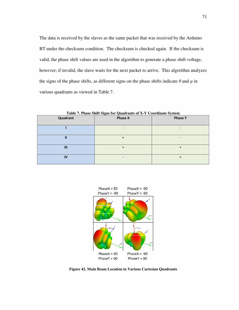
Table 7 Phase Shift Signs for Quadrants of X-Y Coordinate System .................... 71
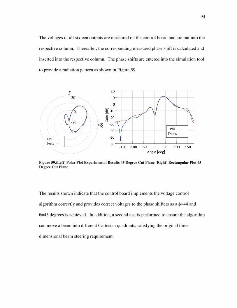
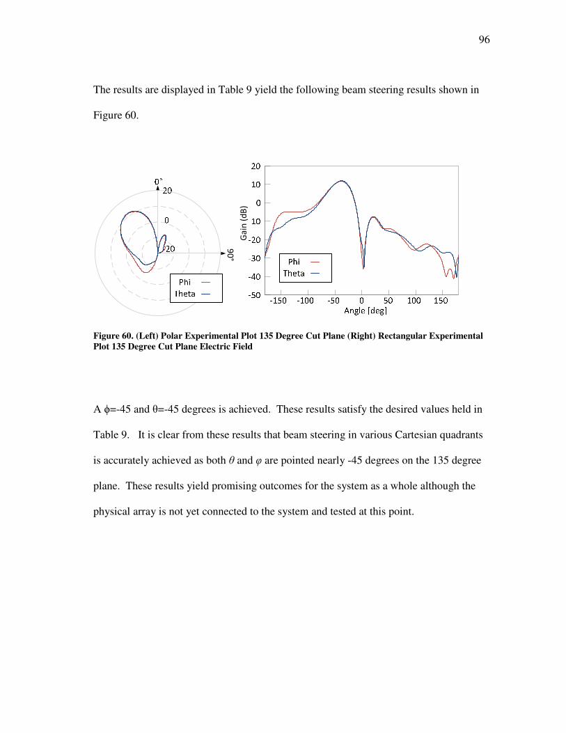
Table 8 First Experimental Result Beam Steering ................................................ 93
Table 9 Second Experimental Result Beam Steering ............................................ 95
Table 10 Measured Results Phi Direction ................................................................ 112
Table 11 Measured Results Theta Direction ............................................................ 112
Page 17
1
CHAPTER I
INTRODUCTION
As an integral part of many complex communications systems, phased arrays provide a
technical enhancement in beam steering that single antenna arrays cannot provide. In
lieu of mechanically steering an antenna by physically moving its radiating surface in a
desired direction, the same objective may be achieved through electrical control without
mechanical intervention. Through various control methods [1-3] the progressive phase
shift of individual array elements is controlled to achieve directional beam steering that
is found in many applications such as satellite, military, and commercial applications.
PAVE PAWS, a U.S. military defense system, uses phased array radar to detect missiles
and other objects in space by steering a beam from single locations [4]. In another
example, the MESSENGER spacecraft is currently performs deep space missions which
utilize a linearly polarized phased array for communications from Mercury to Earth [5].
While the concept of phased arrays or directional antenna transmission was originally
developed more than 100 years ago [6], progressive research of array fabrication,
development of control circuitry and algorithms, and design of electromagnetic
components have allowed phased arrays to evolve to what they are today. Without
continued research, phased arrays would not possess necessary technical enhancements
such as multi-beam steering or cost-effective implementation of radio control networks
[7].
____________
This thesis follows the style of IEEE Transactions on Antennas and Propagation.
Page 18
2
As new technology becomes available, it is important to continue to develop and
integrate these new technologies into phased array systems to further enhance their
efficiency and operability, further introducing phased arrays into new communication
domains.
Smart phones, although widely viewed as mobile entertainment devices, carry many
useful electrical tools that are often found in complex networks. Sensors, memory,
processors, and wireless communications hardware are fundamental components of
information networks today. Naturally, smart phones have the capability to be
integrated into the future of cognitive radio networks, as their presence has been seen
into the integration of energy management, automation and control, and other fields as
tools that gather information or implement signal controls. Many Android applications
such as in literature [8] allow a user to control and monitor vital functions of their home
such as air conditioning, humidity, lighting, and other electrical systems with their
phone. As pervasive use of smart phones and tablets continues in society, there should
exist to some extent, an integration of these devices into academia and in particular,
engineering research of many types. As a new technology, smart phones offer new
possibilities of integration into complex communications systems as the primary
computing resource, allowing conventional systems to become more mobile and new
systems to emerge as communication networks of the future. These thoughts were
conceived more than 40 years ago best said by F. J. Langley, “Low cost commercial
Page 19
3
microcomputers, (currently used in many diverse applications, e.g. point-of-sale
terminals, desk top computers, check processors, etc.), … provide the opportunity for
computing beam steering and shaping phase shifts for large phased-array antennas …”
[9].
This research promotes the future of phased array development by integrating a smart
phone into a conventional phased array control method. As aforementioned, smart
phones have become integral in society in the last decade and their mobile computing
prowess provides a natural assimilation into a conventional phased array control method.
Some immediate advantages provided by this research are the capability to bring
conventional phased array control methods into a new domain by providing a powerful
mobile computing resource and to introduce smart phones as a pivotal research tool in
future electromagnetics research. Furthermore, the ability to program the smart phone
allows for multiple modes of operation of the control network, by either allowing a
human operator to directly control the beam direction in the palm of their hand or setting
the phone into an autonomous control mode with little to no human interaction. With
this knowledge and capability, this research provides new insight and understanding to
controlling phased arrays and serves as an innovative implementation of a fundamental
technology.
Page 20
4
CHAPTER II
SURVEY
Tracking an object using antennas was, for a long time, mechanically instrumented by
physical rotation. To this end, radar and other antenna tracking systems could be
optimized by machinery to track an object through space whether static or in motion.
Coinciding with these efforts were groups of engineers that performed math and
calculated an object’s projected path through space to steer antenna beams in the
appropriate direction. However, upon realization of electronic beam steering using
phased arrays coupling advancements in development with computing technology,
tracking algorithms for phased arrays have exceedingly progressed far beyond the
mechanical predecessors [10]. Algorithms for phased array on different surfaces such as
ground, water and air have been developed to track objects in space to avoid collision,
detect intrusion or track an object. Heavily found in military applications, object
tracking algorithms primarily serve to detect missiles or flying objects; whereas, other
applications extend to tracking an object such as a satellite, to maintain a line of sight
communication channel as it passes through space. For all applications, it is necessary
to survey relevant literature that tracks an object to help further explain the advantages
of a system integrated smartphone leading to exciting future work of this project.
Fundamentally, tracking any object, whether static or moving, requires information to be
analyzed by a control system. Many authors attempt object tracking methods using
Page 21
5
more complex schemes with filters that analyze object history, while some adapt basic
control theory concepts to estimate the state of an object as it moves through space.
Questions of uncertainty such as location of the object, future movement of the object,
future movement of the tracker, system sampling rate and so on, have provided
researchers an extensive task of developing an accurate control methodology. In order
to develop a control method, arbitrary or unknown system variables need to be estimated
or ignored. One method of doing this is to apply a basic Kalman filter [10-13]. Kalman
filters analyze a history of data to predict the future state of the system [10-13]. In one
such algorithm using an alpha-beta filter, the refresh rate time is set constant to
determine the system update rate while assuming that the input measurement, or target
state, is known for every measurement [10, 12]. This simplifies the Kalman filter
equations and provides an estimation of state upon choosing appropriate linear values of
alpha and beta. The Kalman filter approach also assumes that there is a single
measurement input and that this input is a linear function of the target state. In the case
of tracking an object, this filtered approach would allow the system to estimate the
target’s new position based on its current path and would therefore reconfigure the
phased array to track this target.
In another approach, it can be assumed that the system has some distribution of Gaussian
noise which could be sourced from many references such as measurement interference
or unknown state of the measurement. It is necessary to then choose a measurement of
the target that is based on practical data association [10, 11, 14]. The Nearest Neighbor
Page 22
6
(NN) algorithm provides a probability association of measurement data to a set of
predicted measurements, where the measurement received is compared to the next
closest predicted measurement and is validated [14]. This model reflects a practical
application of tracking an object from a system that is in the presence of noise such as a
changing non-linear position as given during an object’s acceleration. The NN
algorithm can be coupled with a Kalman filter to provide a multiple layered algorithm
that reflects a validation of the measurement in addition to tracking the object’s position
based on its previous position or state.
In other related studies, many filters have been combined to aggregate noise cancellation
and reduce unknown variables for tracking objects in the Interacting Multiple Model
(IMM) algorithm [15]. The IMM algorithm performs exceptionally well in tracking
objects at high speeds and when performing arbitrary maneuvers. Comprised on a basis
of Markov chain models, the IMM algorithm determines the object’s state by comparing
multiple filter outputs and determining the objects state by combining the outputs
coupled with data association [15]. Each model has advantages and disadvantages
tracking an object. This survey of works demonstrates the active participation of
research in this field and incorporates the phased array control model into computations
and algorithms.
Page 23
7
CHAPTER III
BACKGROUND
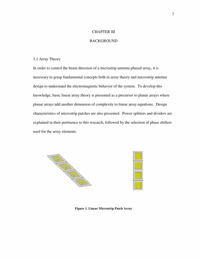
3.1 Array Theory
In order to control the beam direction of a microstrip antenna phased array, it is
necessary to grasp fundamental concepts both in array theory and microstrip antenna
design to understand the electromagnetic behavior of the system. To develop this
knowledge, basic linear array theory is presented as a precursor to planar arrays where
planar arrays add another dimension of complexity to linear array equations. Design
characteristics of microstrip patches are also presented. Power splitters and dividers are
explained in their pertinence to this research, followed by the selection of phase shifters
used for the array elements.
Figure 1. Linear Microstrip Patch Array
Page 24
8
Linear arrays, as shown in Figure 1, provide the fundamental equations needed to
analyze phased arrays. To adequately address the operation of linear arrays, the
formulation of an array factor may be found by the superposition of electric fields from
periodic spaced antenna elements. If each element has equal amplitude and has a
progressive phase shift β, the array is said to be a uniform array [16]. If the elements are
considered to be point sources, the array factor for an N element linear array is shown by
sin( )21
sin( )2
N
AF
ψ
ψ
=
(0.1)
where the character ψ is represented by
cos( )kdψ θ β= + (0.2)
The realization of (0.1) is the compact form of the array factor for an N element array.
To normalize the array factor among the number of elements, (0.1) is divided by the total
number of elements N shown by
sin( )1 2
1sin( )
2
N
AFN
ψ
ψ
=
(0.3)
The calculation of the array factor is necessary as it is used in calculating the total array
pattern by multiplying it with a single element pattern. From this formulation, the theory
is used to help determine phase shifts to steer the beam in Euclidean space. In this
research, the beam is always configured to radiate at a maximum along an axis that is
normal to the surface of the antenna array, which is referred to as broadside [16]. To
Page 25
9
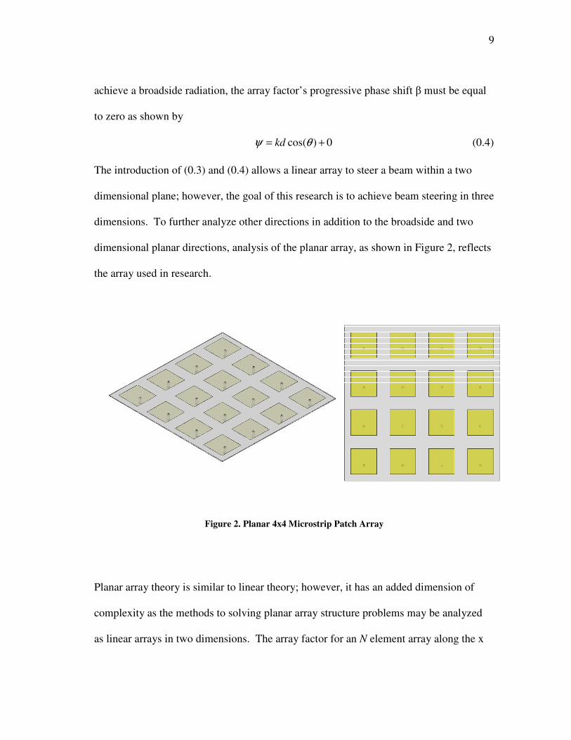
achieve a broadside radiation, the array factor’s progressive phase shift β must be equal
to zero as shown by
cos( ) 0kdψ θ= + (0.4)
The introduction of (0.3) and (0.4) allows a linear array to steer a beam within a two
dimensional plane; however, the goal of this research is to achieve beam steering in three
dimensions. To further analyze other directions in addition to the broadside and two
dimensional planar directions, analysis of the planar array, as shown in Figure 2, reflects
the array used in research.
Figure 2. Planar 4x4 Microstrip Patch Array
Planar array theory is similar to linear theory; however, it has an added dimension of
complexity as the methods to solving planar array structure problems may be analyzed
as linear arrays in two dimensions. The array factor for an N element array along the x
Page 26
10
axis of (0.5), is the summation of the current distribution for each linear element, where
elements have an equal spacing of dx and a progressive phase shift βx.
( 1)( sin cos )
0
1
x x
Nj m kd
x
n
AF I eθ φ β− +
=
=∑ (0.5)
The directional cosine sinθcosφ accounts for the phase separation of linear elements
along the x axis in Cartesian coordinates that observe a point in spherical coordinates.
Now, consider a similar array that is parallel along the y axis represented by
( 1)( sin sin )
0
1
y y
Mj n kd
y
m
AF I eθ φ β− +
=
=∑ (0.6)
where dy is the spacing between elements, βy is the progressive phase shift and sinθsinφ
is the directional cosine along the y axis. To find the total array factor for an M by N
element array, a dot product of (0.5) and (0.6) yields
( 1)( sin sin ) ( 1)( sin cos )
0 0
1 1
y y x x
N Mj m kd j n kd
x y
n m
AF I I e eθ φ β θ φ β− + − +
= =
=
∑ ∑ (0.7)
The directional cosines were derived using the relationship
^ ^
^ ^
sin cos
sin sin
x r
y r
θ φ
θ φ
⋅ =
⋅ =
(0.8)
The compact normalized form of the total array factor is
sin( ) sin( )1 12 2( , )
sin( ) sin( )2 2
yx
nx y
M N
AFM N
ψψ
θ φψ ψ
= ⋅
(0.9)
where ψx,ψy are represented in equation (0.2). The formulation of (0.9) realizes that the
maximum location is dependent from θ and φ. The primary concern of this research is to
Page 27
11
point the primary beam in the direction of an object using a primary θ and φ. If these are
known, the progressive phase shift for individual array elements can be calculated by
sin cos
sin sin
x x x
y y y
kd
kd
ψ θ ϕ β
ψ θ ϕ β
= +
= + (0.10)
The fundamental calculations in all algorithms use (0.10) provided further assumptions.
Beam width, side lobes and other array characteristics are not factored into equations
and calculations as they are not concerned with the primary goal of this research. Using
(0.10), the individual phase shifts may be calculated by realizing that maximums of
(0.10) occur under the conditions shown in (0.11).
2
2
x
y
m
n
ψ π
ψ π
+=
+=
(0.11)
From (0.11), it is clear that the maximums occur when both m and n are equal to 0.
From before, (0.10) now becomes (0.12).
0 0
0 0
sin cos
sin sin
x x
y y
kd
kd
β θ ϕ
β θ ϕ
= −
= − (0.12)
With this analysis, individual phase shifts are calculated by using (0.12) directly in the
smart phone’s code. This fundamental theory and analysis provides the essentials to
understanding linear and planar arrays. Although the arrays shown in Figure 1 and
Figure 2 are comprised of patch antennas, arrays utilize many other types of antennas
such as wire dipoles and other microstrip dimensional forms. However, this research
utilizes microstrip rectangular patch antennas which require analysis to understand the
single element operation.
Page 28
12
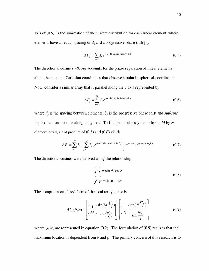
In order to fabricate a planar array, it is necessary to consider the individual antenna
element type. A simple structure used in many applications is the microstrip patch
antenna [16]. Microstrip patch antennas, as shown in Figure 3, are notably directional
antennas as the primary concentration of their radiation pattern exists along an axis
normal to the radiating boundary. Their existence and function has been explained
through much research and they are commonly used today [16-18]. The composition of
this antenna is typically a copper strip in a geometric shape such as a rectangle or circle
that sits upon a dielectric slab and ground plane [16]. Typical current feeds for patch
antennas are through microstrip lines or probes. This research considers only a
rectangular microstrip patch that is probe fed.
L
W
d(µ1,ε1)
t
Figure 3. Microstip Patch with Design Parameters
Page 29
13
The design parameters for microstrip patch antennas focus on dimensional
characteristics of the copper upon the dielectric. Initial design characteristics are
concerned primarily with these factors: width, length, dielectric constant, probe position
and operating frequency [16]. The width W, length L, probe spacing d, and dielectric
thickness t, are shown in Figure 3. Probe spacing calculations require additional
complex mathematics that will not be discussed in this work. Simulation optimization
techniques are used to determine the final probe placement values. The thickness or
height of the substrate is dependent on manufacturer design. It can be shown that the
width required for an operating frequency is given by
2
2 1r r
cW
f ε=
+ (0.13)
where c is the speed of light in air, fr is the desired resonance frequency and εr is the
dielectric constant. The length can be calculated using
0 0
1
2r reff
Lf ε µ ε
= (0.14)
where fr is the desired resonant frequency, εreff is the effective dielectric constant
represented by (0.15)
1/21 1
1 122 2
r rreff
h
W
ε εε
−+ −
= + + (0.15)
The basic design requirements are sufficient for this research to produce a fabricated
antenna that produces necessary results. With this basic analysis, the fundamentals for
array design and fabrication are supported. Other realizations of network components
are now examined to complete the system. With this in mind, array theory required that
Page 30
14
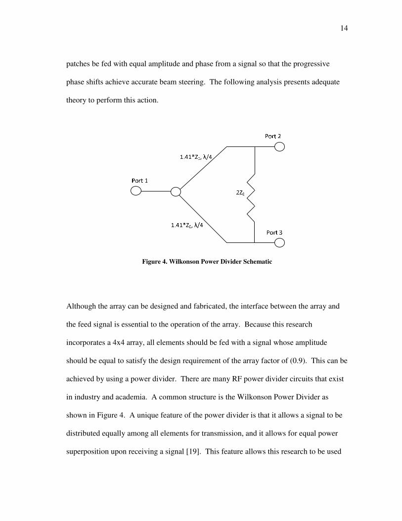
patches be fed with equal amplitude and phase from a signal so that the progressive
phase shifts achieve accurate beam steering. The following analysis presents adequate
theory to perform this action.
Figure 4. Wilkonson Power Divider Schematic
Although the array can be designed and fabricated, the interface between the array and
the feed signal is essential to the operation of the array. Because this research
incorporates a 4x4 array, all elements should be fed with a signal whose amplitude
should be equal to satisfy the design requirement of the array factor of (0.9). This can be
achieved by using a power divider. There are many RF power divider circuits that exist
in industry and academia. A common structure is the Wilkonson Power Divider as
shown in Figure 4. A unique feature of the power divider is that it allows a signal to be
distributed equally among all elements for transmission, and it allows for equal power
superposition upon receiving a signal [19]. This feature allows this research to be used
Page 31
15
both for transmission and reception purposes. Instead of designing a 16 split trace
Wilkonson power divider, a divider was purchased from Instock Wireless Components
with the following specifications [36].
Table 1. Instock Wireless Components Power Divider Specifications
Frequency Impedance Insertion Loss Amplitude Balance Phase Balance
.7-2.7 GHz 50 Ohms 1.8 dB (max) .6 dB (max) 10 Degrees (max)
These specifications suffice the basic need of the system. Before the signal can be sent
to the individual radiating elements, the proper phase shift must be applied to achieve
correct beam steering. Analysis of phase shifter operation is necessary to understand the
implications in network operation. Physical analysis of a phase shifter is not discussed
in this research.
Page 32
16
Figure 5. Hittite Analog Phase Shifter (2-4 GHz) with Evaluation Board
After the signal has been distributed through the power divider, it must pass through a
phase shifter before arriving at the radiating patch. The phase shifters chosen for this
project are from Hittite Corporation. As analog phase shifters, they require a control
voltage ranging from 0-12 Volts which thereby produces a respective phase shift from 0
to 450 degrees as shown in Figure 6 .
Page 33
17
Figure 6. Hittite Phase Shifter Voltage Control of Phase Shift
The system requires that a phase shift be related to a voltage. To do this accurately, it is
necessary to approximate the graph in a linear manner to design simple algorithms at the
control level. An equation relating the desired phase shift to an expected voltage is
required at the control level to achieve beam steering.
Vo
lta
ge
(V
)
Figure 7. Hittite Phase Shifter Approximation with Equation
Page 34
18
From Figure 7, an approximation for an input phase related to the voltage is provided in
the equation which is also listed below.
3 28 08*deg 8 05*deg 0.005*deg 0.1039Voltage E E= − − + − + + (0.16)
(0.16) is tested in the algorithm as a first pass to determine whether this approximation
will provide sufficient control. The variable deg is the input degree value that is
converted to a voltage output. Electromagnetic hardware design and analysis has been
presented. Given a proper beam shift capability of the system, the algorithms require
and object or direction to reference in Euclidean space. Discussion of basic mathematic
point determination and rotation is discussed.
Provided the relevant background of antenna arrays, microstrip patch design, power
dividers and phase shifters, it is important to highlight brief mathematic calculations to
determine essential information for the system. Because this system needs to track
objects and steer the main beam in three dimensional space, there exists a need to relate
a position to angles θ0 and φ0 to be used in (0.12). This can be done in a number of ways
such as Pythagorean’s Theorem, change of coordinates, or directional cosines. In this
case, the Pythagorean Theorem presents a straightforward approach to calculating
position and direction for the system. To begin, it is assumed that a point in space has a
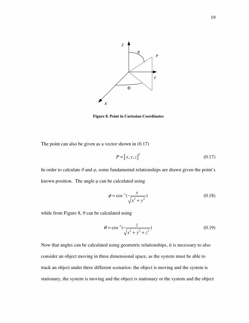
known position of (x ,y ,z) with respect to the origin as shown in Figure 8.
Page 35
19
Φ
θ P
Y
Z
X
Figure 8. Point in Cartesian Coordinates
The point can also be given as a vector shown in (0.17)
[ ], ,T
P x y z= (0.17)
In order to calculate θ and φ, some fundamental relationships are drawn given the point’s
known position. The angle φ can be calculated using
1
2 2cos ( )
x
x yφ −=
+ (0.18)
while from Figure 8, θ can be calculated using
1
2 2 2cos ( )
z
x y zθ −=
+ + (0.19)
Now that angles can be calculated using geometric relationships, it is necessary to also
consider an object moving in three dimensional space, as the system must be able to
track an object under three different scenarios: the object is moving and the system is
stationary, the system is moving and the object is stationary or the system and the object
Page 36
20
are both moving. Under any circumstance, it is simple to always consider that the
system is static so as to maintain a constant coordinate system. Thus, whether the
system or the object is moving, it can be modeled as the object moving in space using a
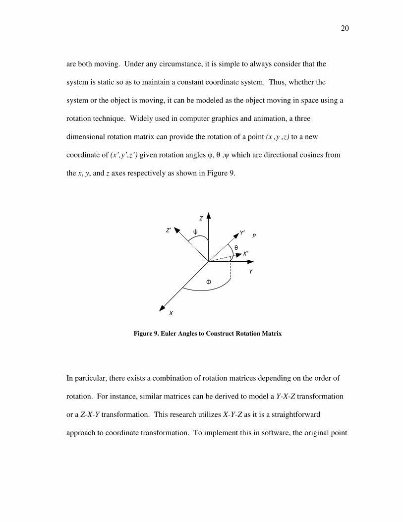
rotation technique. Widely used in computer graphics and animation, a three
dimensional rotation matrix can provide the rotation of a point (x ,y ,z) to a new
coordinate of (x’,y’,z’) given rotation angles φ, θ ,ψ which are directional cosines from
the x, y, and z axes respectively as shown in Figure 9.
Φ
θ
P
Y
Z
X
ψ
X’
Y’Z’
Figure 9. Euler Angles to Construct Rotation Matrix
In particular, there exists a combination of rotation matrices depending on the order of
rotation. For instance, similar matrices can be derived to model a Y-X-Z transformation
or a Z-X-Y transformation. This research utilizes X-Y-Z as it is a straightforward
approach to coordinate transformation. To implement this in software, the original point
Page 37
21
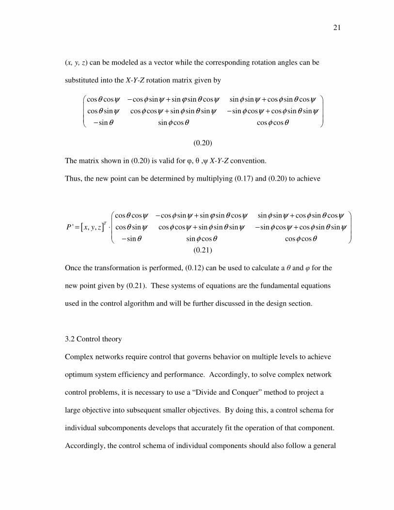
(x, y, z) can be modeled as a vector while the corresponding rotation angles can be
substituted into the X-Y-Z rotation matrix given by
cos cos cos sin sin sin cos sin sin cos sin cos
cos sin cos cos sin sin sin sin cos cos sin sin
sin sin cos cos cos
θ ψ φ ψ ϕ θ ψ φ ψ φ θ ψ
θ ψ φ ψ φ θ ψ φ ψ φ θ ψ
θ φ θ φ θ
− + +
+ − + −
(0.20)
The matrix shown in (0.20) is valid for φ, θ ,ψ X-Y-Z convention.
Thus, the new point can be determined by multiplying (0.17) and (0.20) to achieve
[ ]cos cos cos sin sin sin cos sin sin cos sin cos
' , , cos sin cos cos sin sin sin sin cos cos sin sin
sin sin cos cos cos
TP x y z
θ ψ φ ψ ϕ θ ψ φ ψ φ θ ψ
θ ψ φ ψ φ θ ψ φ ψ φ θ ψ
θ φ θ φ θ
− + +
= ⋅ + − + −
(0.21)
Once the transformation is performed, (0.12) can be used to calculate a θ and φ for the
new point given by (0.21). These systems of equations are the fundamental equations
used in the control algorithm and will be further discussed in the design section.
3.2 Control theory
Complex networks require control that governs behavior on multiple levels to achieve
optimum system efficiency and performance. Accordingly, to solve complex network
control problems, it is necessary to use a “Divide and Conquer” method to project a
large objective into subsequent smaller objectives. By doing this, a control schema for
individual subcomponents develops that accurately fit the operation of that component.
Accordingly, the control schema of individual components should also follow a general
Page 38
22
control schema for the entire system so that subcomponents mesh efficiently as a whole
during operation. These fundamental concepts provide significant advantages for the
system designer in that the project may be built in a modular fashion, thereby setting
achievable milestones that provide functional network components. Furthermore, the
control concepts and design of each module or subcomponent becomes formidably
easier as the complex problem divides into simpler problems.
Divide and conquer is a methodology or practice that is commonly found in many
aspects of problem solving. For the purpose of this research, divide and conquer will be
associated in definition most closely with that found in the field of computer science,
particularly algorithm development [21]. Because this project implements software
algorithms to implement control theory, it is fitting to use this association. Divide and
conquer has two specific approaches that will be referenced in this research.
The first method derives from an approach to recursively divide a problem into
subcomponents using a specific method continuously until the problem becomes directly
solvable. This assumes that while the original problem could possibly be solved from
induction or a complex algorithm, repeating a process at subsequent stages reduces the
problem to a simplified basic solution which applies to all other subdivisions. This
method of divide and conquer assumes that each subsequent stage contains similar
problems to the stage before. An example of this type of divide and conquer is in a
Page 39
23
binary search algorithm. Take the following list of random numbers that have been
sorted from smallest to largest shown in Figure 10.
Figure 10. Random Ordered List of Numbers
The goal of this divide and conquer approach is to find the position of a given number
by randomly picking a position in the list of numbers and asking a yes or no question “Is
number greater than this random position?”. Here, the method of divide and conquer is
the yes or no question and is performed at subsequent stages until the exact number is
found. Thus, the number 46 is to be found in the list. A number 60 is chosen from the
list and is compared with 46. Because 46 is less than 60, all numbers greater than 60 are
eliminated from the search. Now, a new number 51 is selected from the remaining
numbers and is compared to 46. Thus, 46 is still less than 51 so all numbers greater than
51 are again eliminated. This process is recursive until the number selected equals 46.
In the same way, problems in this research are divided recursively until directly solved.
The second method takes a complex problem and divides it into subcomponents that are
different from each other but are more directly solvable than the original problem.
Fundamentally, this method uses a more theoretical sense to solve a problem, rather than
being specifically implemented in software; however, this methodology allows a
Page 40
24
complex problem to become modular and as aforementioned, sets achievable goals that
are integral to the development of a solution. For example, an engineering team
comprised of electrical, mechanical, and chemical engineers works on a project.
Because each group is specialized in a particular area of engineering, it is only logical to
take the project goal and subdivide it into simpler projects for each team to solve
separately. Upon completion of each subcomponent by the respective engineering team,
the project compiles together to function as a whole. This method of divide and conquer
is most often referenced in this research as a way to develop modular control theories
and algorithms. In addition to divide and conquer methodologies, it is necessary to
introduce a fundamental concept in control theory itself that is relevant to this project.
In order to control a system, there exists some knowledge or data about the system with
which the control algorithm can analyze to determine the respective output.
Fundamentally, every system has some type of data flow from input to output; however,
the control used to determine the output from the input may be different. Accordingly, it
is necessary to present two different control methodologies and correlate the usage of
one method into this research.
The first control method is referred to as open loop control, and it is the control
methodology that is used in this project. Open loop control requires no previous
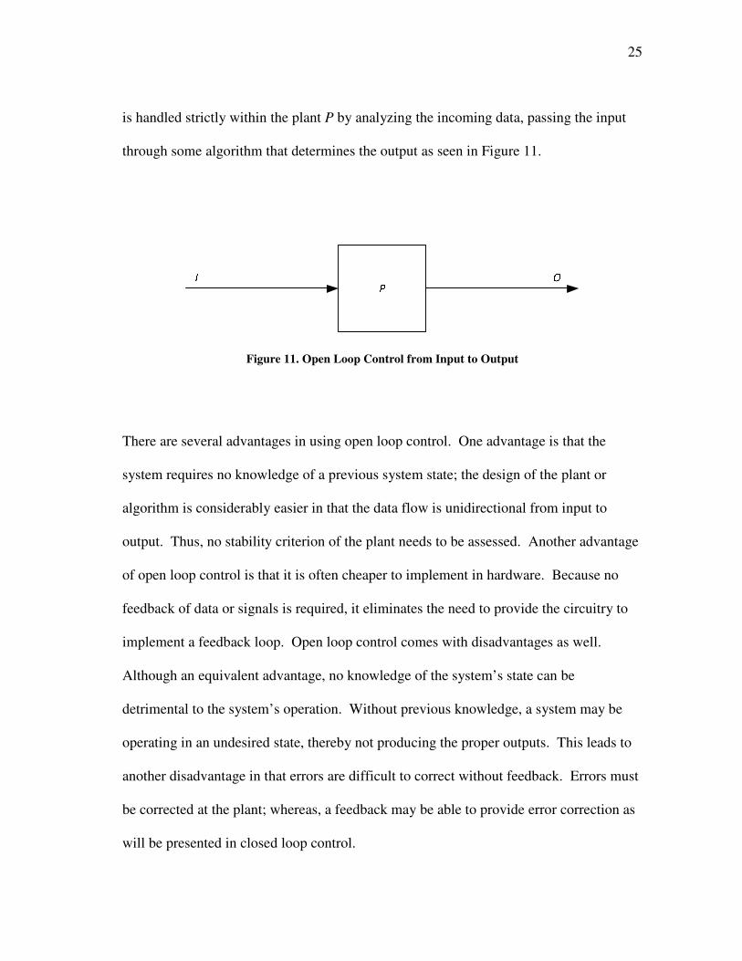
estimation of the system’s operating state [22]. The data arrives at an input I and then
travels through a control plant P, and then flows to the output O. Control of the system
Page 41
25
is handled strictly within the plant P by analyzing the incoming data, passing the input
through some algorithm that determines the output as seen in Figure 11.
Figure 11. Open Loop Control from Input to Output
There are several advantages in using open loop control. One advantage is that the
system requires no knowledge of a previous system state; the design of the plant or
algorithm is considerably easier in that the data flow is unidirectional from input to
output. Thus, no stability criterion of the plant needs to be assessed. Another advantage
of open loop control is that it is often cheaper to implement in hardware. Because no
feedback of data or signals is required, it eliminates the need to provide the circuitry to
implement a feedback loop. Open loop control comes with disadvantages as well.
Although an equivalent advantage, no knowledge of the system’s state can be
detrimental to the system’s operation. Without previous knowledge, a system may be
operating in an undesired state, thereby not producing the proper outputs. This leads to
another disadvantage in that errors are difficult to correct without feedback. Errors must
be corrected at the plant; whereas, a feedback may be able to provide error correction as
will be presented in closed loop control.
Page 42
26
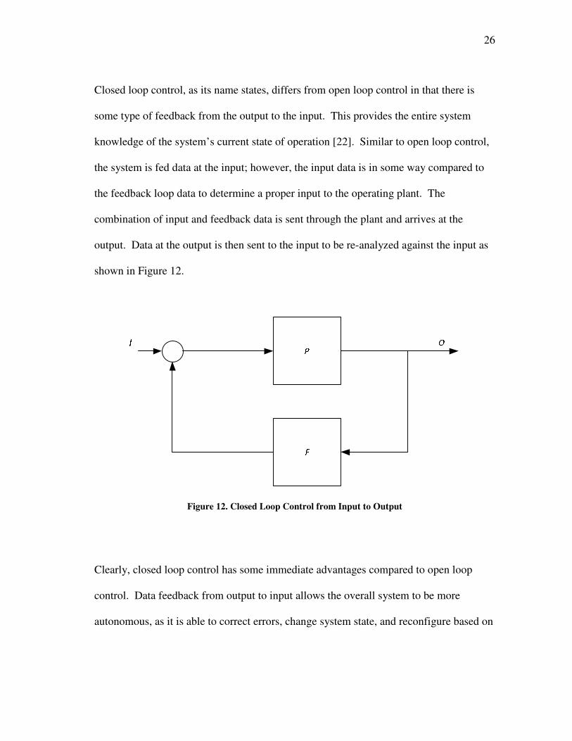
Closed loop control, as its name states, differs from open loop control in that there is
some type of feedback from the output to the input. This provides the entire system
knowledge of the system’s current state of operation [22]. Similar to open loop control,
the system is fed data at the input; however, the input data is in some way compared to
the feedback loop data to determine a proper input to the operating plant. The
combination of input and feedback data is sent through the plant and arrives at the
output. Data at the output is then sent to the input to be re-analyzed against the input as
shown in Figure 12.
Figure 12. Closed Loop Control from Input to Output
Clearly, closed loop control has some immediate advantages compared to open loop
control. Data feedback from output to input allows the overall system to be more
autonomous, as it is able to correct errors, change system state, and reconfigure based on
Page 43
27
operating state information. Consequently, inherent disadvantages also come from
closed loop control. The plant is more difficult to design as it must meet a different set
of stability criterion as it analyzes both input and feedback data. Comparable to open
loop control, there may be a need for additional circuitry in the feedback loop,
depending on what type of feedback is needed.
Although open and closed loop control has their respective advantages and
disadvantages, open loop control will be primarily used in this research for a couple of
reasons. First, this project primarily serves to explore a proof of concept. As such, a
design of system feedback as found in closed loop control would amplify the difficulty
of the original project goal and may hinder the success of showing proof of concept. In
addition, open loop control is implementable into available circuitry that is used in this
project.
3.3 Control circuitry
Hardware is an implementation for network theory and concepts, complementing
intangible equations and processes by bringing these elements into a physical,
measurable environment. In this research, hardware implementation has many different
components with variable functionality. This section serves to provide the reader with a
background of individual circuit elements in order to understand the physical role that
each individual piece of hardware plays; as well as, introduce potential platforms and
capabilities of hardware components that the system uses as a whole.
Page 44
28
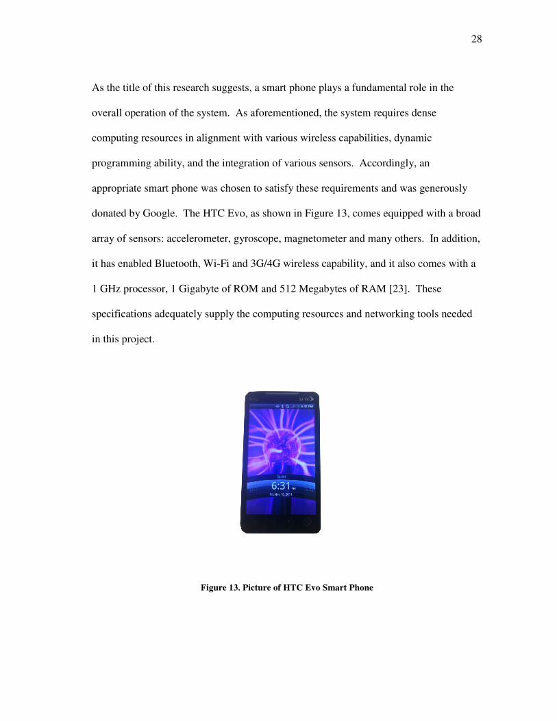
As the title of this research suggests, a smart phone plays a fundamental role in the
overall operation of the system. As aforementioned, the system requires dense
computing resources in alignment with various wireless capabilities, dynamic
programming ability, and the integration of various sensors. Accordingly, an
appropriate smart phone was chosen to satisfy these requirements and was generously
donated by Google. The HTC Evo, as shown in Figure 13, comes equipped with a broad
array of sensors: accelerometer, gyroscope, magnetometer and many others. In addition,
it has enabled Bluetooth, Wi-Fi and 3G/4G wireless capability, and it also comes with a
1 GHz processor, 1 Gigabyte of ROM and 512 Megabytes of RAM [23]. These
specifications adequately supply the computing resources and networking tools needed
in this project.
Figure 13. Picture of HTC Evo Smart Phone
Page 45
29
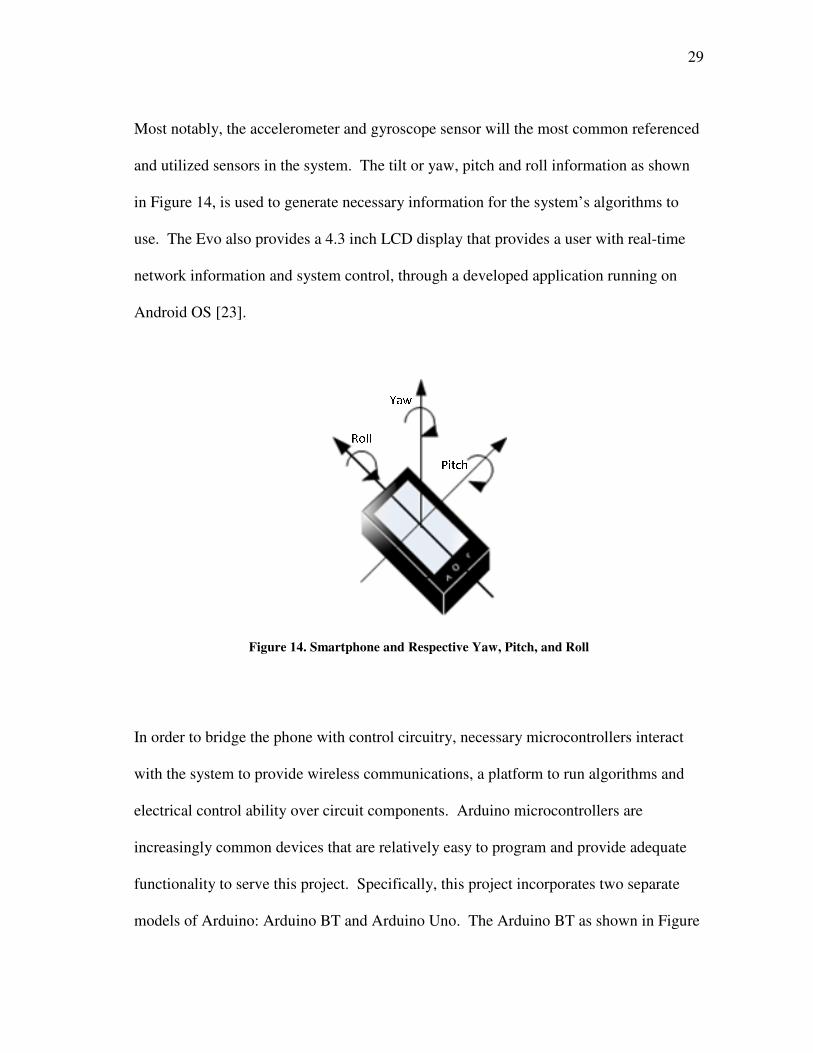
Most notably, the accelerometer and gyroscope sensor will the most common referenced
and utilized sensors in the system. The tilt or yaw, pitch and roll information as shown
in Figure 14, is used to generate necessary information for the system’s algorithms to
use. The Evo also provides a 4.3 inch LCD display that provides a user with real-time
network information and system control, through a developed application running on
Android OS [23].
Figure 14. Smartphone and Respective Yaw, Pitch, and Roll
In order to bridge the phone with control circuitry, necessary microcontrollers interact
with the system to provide wireless communications, a platform to run algorithms and
electrical control ability over circuit components. Arduino microcontrollers are
increasingly common devices that are relatively easy to program and provide adequate
functionality to serve this project. Specifically, this project incorporates two separate
models of Arduino: Arduino BT and Arduino Uno. The Arduino BT as shown in Figure
Page 46
30
15, is a model of the standard Arduino microcontroller with an embedded Bluetooth
receiver. Playing a vital role in establishing a Bluetooth connection with the smart
phone, the Arduino BT also comes with I2C networking capability which will be
explained later in further detail.
Figure 15. Arduino BT (Bluetooth Enabled)
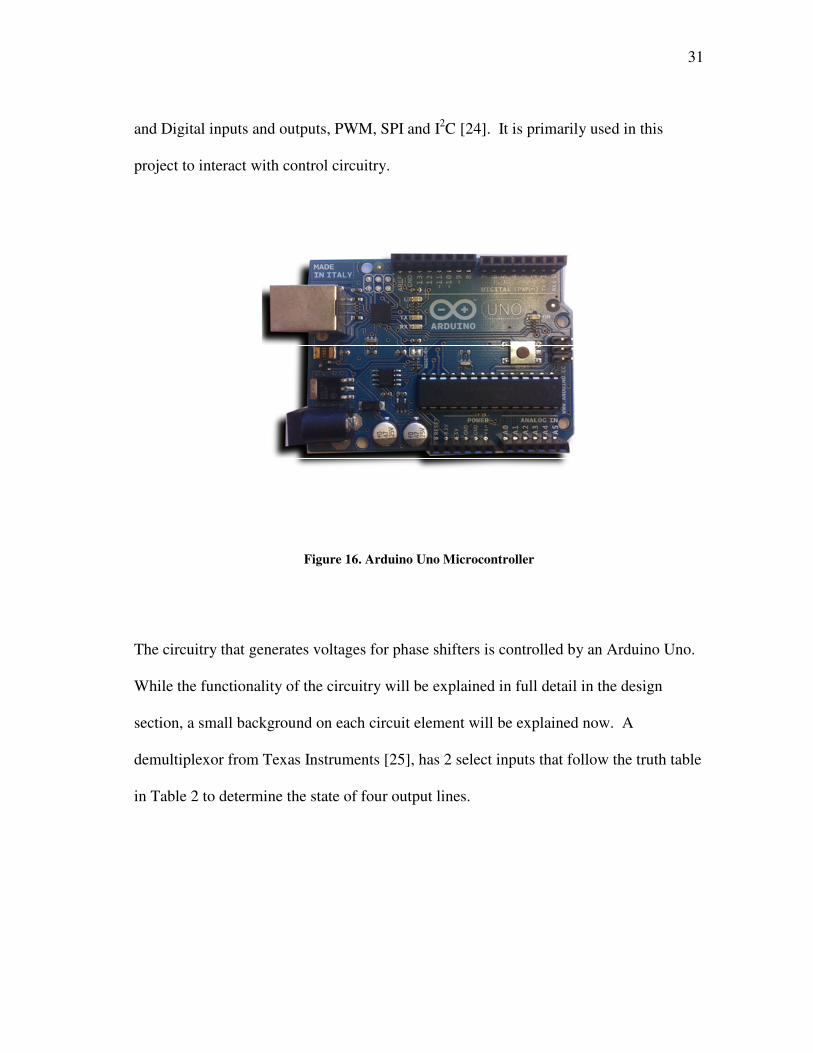
While the Arduino BT interacts with the phone via Bluetooth, it also interacts with
Arduino Uno via I2C. The Arduino Uno as shown in Figure 16, is a standard
microcontroller from the Arduino family that has multiple capabilities including Analog
Page 47
31
and Digital inputs and outputs, PWM, SPI and I2C [24]. It is primarily used in this
project to interact with control circuitry.
Figure 16. Arduino Uno Microcontroller
The circuitry that generates voltages for phase shifters is controlled by an Arduino Uno.
While the functionality of the circuitry will be explained in full detail in the design
section, a small background on each circuit element will be explained now. A
demultiplexor from Texas Instruments [25], has 2 select inputs that follow the truth table
in Table 2 to determine the state of four output lines.
Page 48
32
Table 2. Truth Table for Demultiplexor
Select Input A Input B OUT 0 OUT 1 OUT 2 OUT 3
L X X X X X X
H L L L H H H
H H L H L H H
H L H H H L H
H H H H H H L
A digital potentiometer from Microchip is used to divide the VCC voltage of 5 Volts to
an appropriate voltage between 0 and 5 Volts that is sent to an amplifier stage and the
phase shifters thereafter. The digital potentiometers have onboard memory which can be
written to using an SPI interface. More information on SPI can be found in the next
section. Table 3 shows the digital words that may be written to the digital potentiometer
to set the value of the wiper which controls the voltage at the output [26].
Table 3. Digital Words for Microchip 4131
ACTION DIGITAL WORD
WRITE 0000 00xx xxxx xxxx
READ 0000 11xx xxxx xxxx
INCREMENT 0001 0100
DECREMENT 0001 1000
Page 49
33
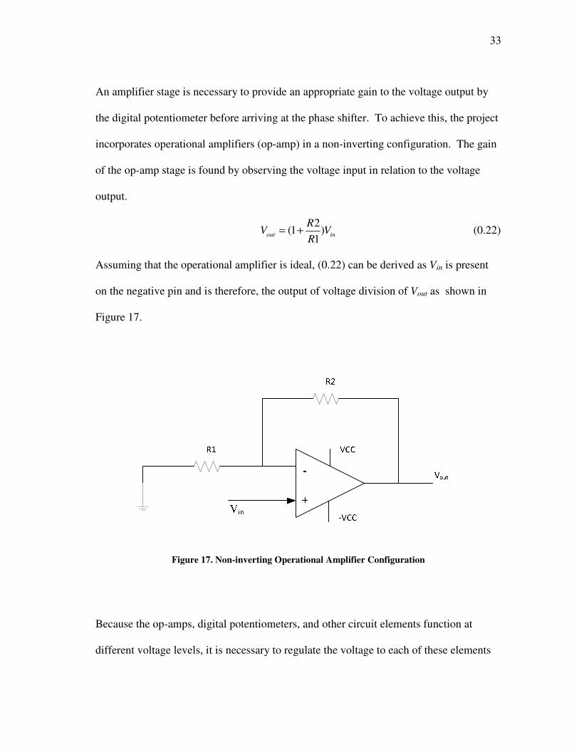
An amplifier stage is necessary to provide an appropriate gain to the voltage output by
the digital potentiometer before arriving at the phase shifter. To achieve this, the project
incorporates operational amplifiers (op-amp) in a non-inverting configuration. The gain
of the op-amp stage is found by observing the voltage input in relation to the voltage
output.
2
(1 )1
out in
RV V
R= + (0.22)
Assuming that the operational amplifier is ideal, (0.22) can be derived as Vin is present
on the negative pin and is therefore, the output of voltage division of Vout as shown in
Figure 17.
Figure 17. Non-inverting Operational Amplifier Configuration
Because the op-amps, digital potentiometers, and other circuit elements function at
different voltage levels, it is necessary to regulate the voltage to each of these elements
Page 50
34
respectively. Voltage regulators from Texas Instruments are selected based on their
voltage and power ratings to supply and regulate voltages of 5 and 12 Volts to the entire
system.
123
Figure 18. Linear Regulator with Pinout (Pin1 - Voltage Input, Pin2 - Ground, Pin3 - Voltage
Output)
3.4 Communications
The ability of hardware to communicate with other hardware is paramount to the
development and success of a control network. More specifically, devices are created by
an array of vendors who often don’t design a product to be used for one purpose;
therefore, there exists a necessary layered communications model in any
communications system that all devices adhere to so that data exchange is possible.
Common practices or implementations of layered communications models are
ubiquitous and many of these implementations interact with one another. A common
referenced model to provide a necessary background is the Open Systems
Interconnection model or commonly referred to as the OSI model. The model was
Page 51
35
initially created by International Organization for Standardization in order to implement
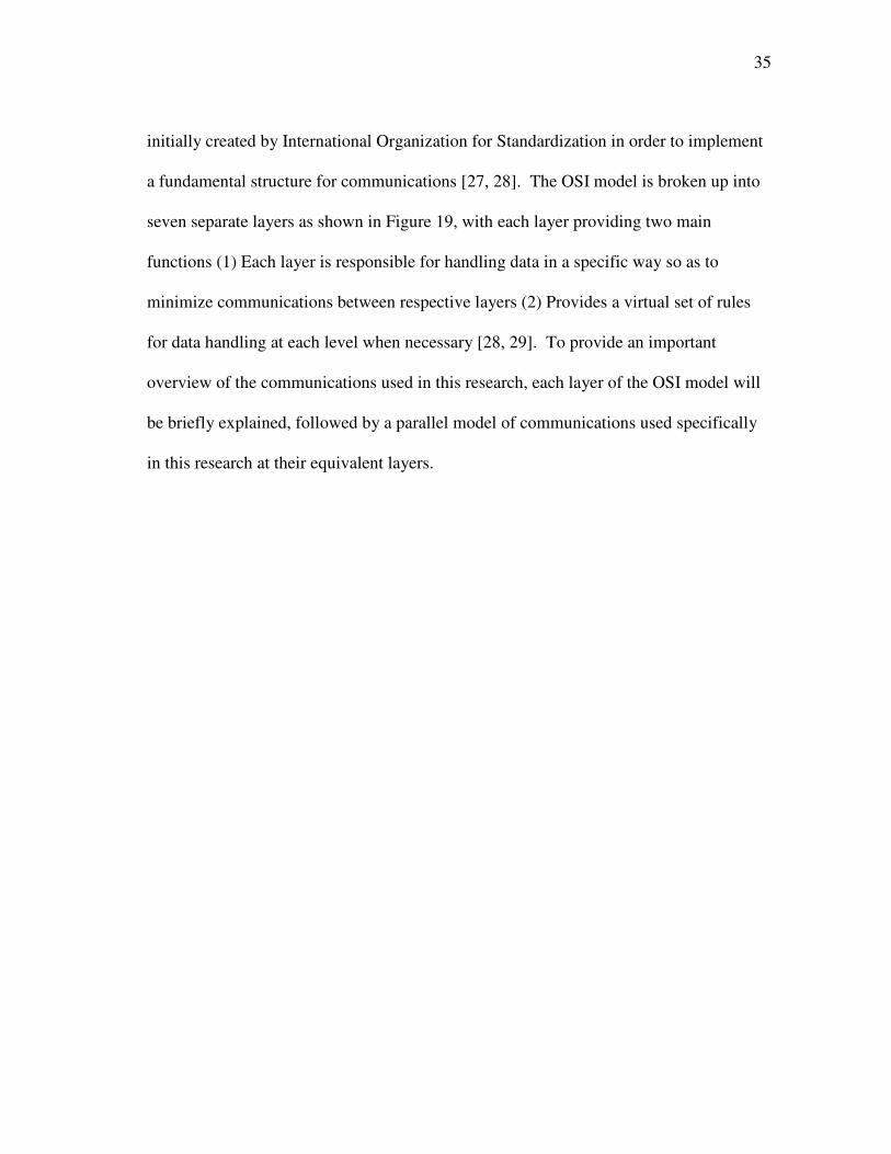
a fundamental structure for communications [27, 28]. The OSI model is broken up into
seven separate layers as shown in Figure 19, with each layer providing two main
functions (1) Each layer is responsible for handling data in a specific way so as to
minimize communications between respective layers (2) Provides a virtual set of rules
for data handling at each level when necessary [28, 29]. To provide an important
overview of the communications used in this research, each layer of the OSI model will
be briefly explained, followed by a parallel model of communications used specifically
in this research at their equivalent layers.
Page 52
36
PHYSICAL LAYER
DATA LINK LAYER
NETWORK LAYER
TRANSPORT LAYER
SESSION LAYER
PRESENTATION LAYER
APPLICATION LAYER
Copper Wire, Optical
Cables, Air
MAC Address, Data
Framing
Routing, Routing
Protocols, Packets
TCP,UDP
HTTP,SMTP,SSH
Transmitting Data
Physical Data Transmission
Receiving Data
Figure 19. OSI Model and Data Flow
The first layer of the OSI model is the Physical Layer or often referred to as PHY. It
serves primarily to establish a physical connection in between two communicating
endpoints and physically send data across this medium. In addition to connecting an
interface to a transmission medium, the PHY layer is also responsible for termination of
Page 53
37
a physical connection, flow control and physical modulation of signals when necessary
[28]. Examples of the PHY layer include and are not limited to copper cables, optical
cables, dielectric materials, wireless communications mediums and many more [29].
The second layer is called the Data Link Layer. Many responsibilities of this layer
include framing of data, detection of physical error connections, flow control and
relative functional communication with a communicating layer two endpoint [28]. This
layer also has a sub-layer within it called Media Access Control or MAC protocol.
MAC addresses are assigned to communicating layer two endpoints to achieve some of
layer two’s responsibilities such as flow control and functional sending of frame data.
These addresses essentially serve as a street address. When sender A in Washington
desires to send mail to receiver B in California, sender A needs an address to send the
mail. MAC addresses provide the same functionality at layer two.
The Network Layer is the third and has the primary responsibilities of routing packets to
communicating layer three devices. This ability and responsibility is important for
routing information in between different sub-networks. Layer three packets differ from
layer two frames in that packets have additional header information that is attached to
data that contains routing and other important layer three information [28]. In addition,
routing protocols and algorithms are implemented at this level to achieve congestion
control, least cost routing and QOS policies. Common examples of network layer
devices include routers and switches [29].
Page 54
38
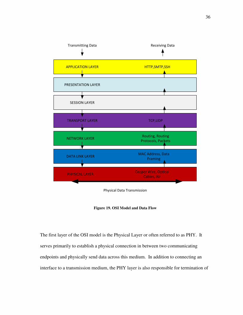
The fourth layer is the Transport Layer. The primary responsibilities of this layer
include the routing error process handling, connection and termination channels of
routing endpoints and network congestion control [28]. Many protocols exist at this
level that handle data flow and error correction in order to improve network efficiency or
maintain data integrity. Common examples of these protocols are found in TCP and
UDP [29]. Whereas TCP has the functionality of handshaking between two endpoints to
ensure data integrity at a slower communication cost, UDP delivers data from one
communicating endpoint to the other as quick as possible at the expense of data integrity
[28].
Sender Receiver
UDP
Sender Receiver
TCP
Figure 20. TCP Versus UDP
Page 55
39
The final fifth through seventh layers are often bundled together as their pertinence into
communication networks is highly dependent on the setup and operability of the
network. The fifth layer is called the Session Layer and is responsible for establishing,
maintaining and terminating remote procedures between computing endpoints [28]. The
sixth layer is called the Presentation Layer and functions as a translator between network
communication layers and the Application Layer which is the seventh layer. The
Application Layer is responsible for implementing many known protocols such as SSH,
Telnet, SMTP and many others [28].
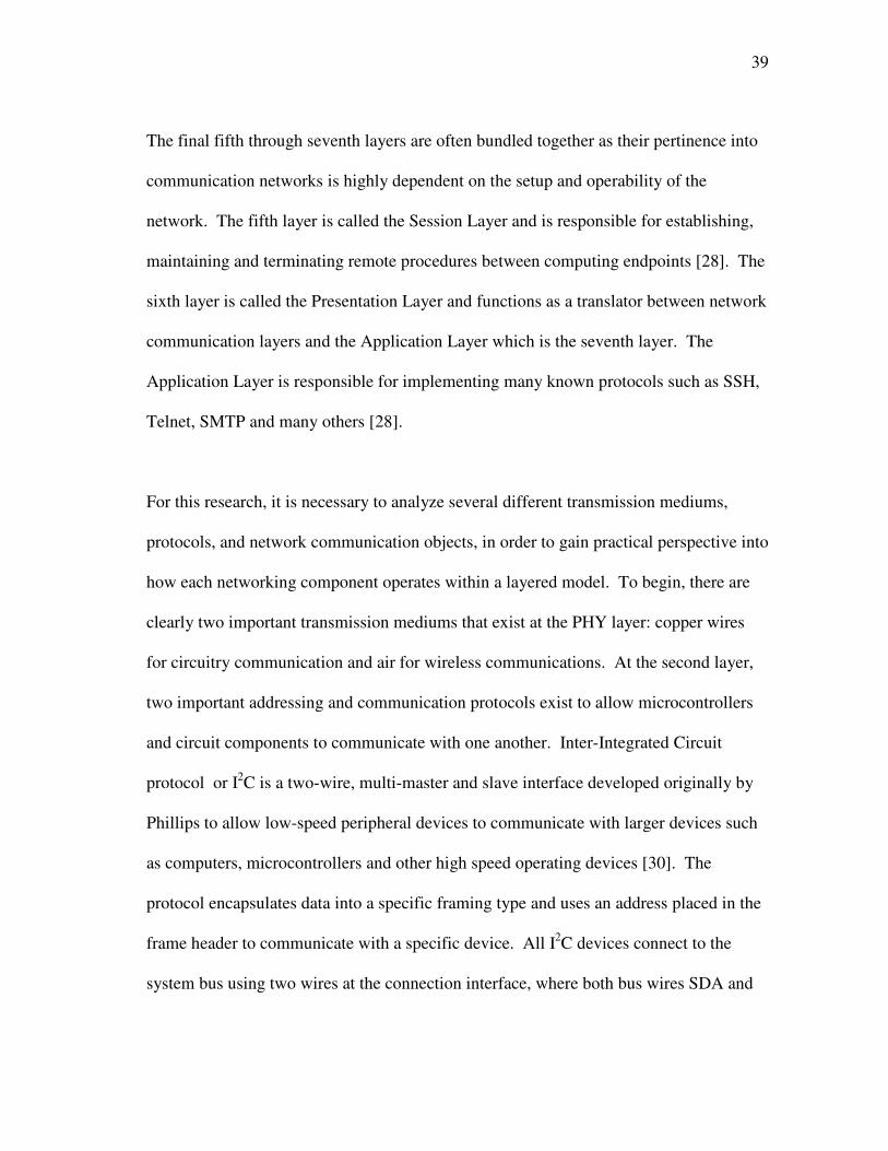
For this research, it is necessary to analyze several different transmission mediums,
protocols, and network communication objects, in order to gain practical perspective into
how each networking component operates within a layered model. To begin, there are
clearly two important transmission mediums that exist at the PHY layer: copper wires
for circuitry communication and air for wireless communications. At the second layer,
two important addressing and communication protocols exist to allow microcontrollers
and circuit components to communicate with one another. Inter-Integrated Circuit
protocol or I2C is a two-wire, multi-master and slave interface developed originally by
Phillips to allow low-speed peripheral devices to communicate with larger devices such
as computers, microcontrollers and other high speed operating devices [30]. The
protocol encapsulates data into a specific framing type and uses an address placed in the
frame header to communicate with a specific device. All I2C devices connect to the
system bus using two wires at the connection interface, where both bus wires SDA and
Page 56
40
SCL are connected to VCC via a pull-up resistor. SCL is used as a clock line which is
generated by a master device connected to the I2C bus and SDA is the data line through
which all data is communicated. As aforementioned, there exist two types of devices
that may connect to the I2C busses. A master device is responsible for setting a system
clock on the SCL line and providing unique 7-bit addresses to all other slave devices on
the network, although this may be alternatively statically configured with each slave. A
slave device connects to the I2C busses sharing the same SCL and SDA as a master
device, and may have a dynamically assigned 7-bit network address or one that is
statically configured. Operation of I2C can be seen from Figure 21.
Figure 21. I2C Network with Master and Two Slaves
Timing is especially important on the I2C bus. Because I
2C is a synchronous protocol, as
all devices transfer data at the rate of the clock speed on SCL, a specific protocol must
be followed. A graphical representation of I2C timing is shown in Figure 22.
Page 57
41
Figure 22. I2C Timing Diagram
The communication process begins with a start condition, labeled S in Figure 22, when
the SDA line goes low and the SCL line maintains high. Next, the data is set on the
SDA line while the SCL line is low and then is sent or read by devices when the SCL
line proceeds high. This continues for the entire data stream and then is stopped by a
condition SP, where SCL maintains high and SDA rises from low to high as shown in
Figure 22. Although I2C is useful for data communications of devices it also comes with
limitations. The 7-bit network address clearly restricts the amount of devices that may
be connected to a single bus. In a larger system with thousands of devices, this may
pose a problem; however, this research doesn’t incorporate this many devices. Another
limitation is the ability to use I2C over large distances, as it is restricted primarily to a
few meters [30]. This too is not a problem in this research, as all the devices are within
half a meter of one another.
Like I2C, another layer two protocol is used to provide communications between the
microcontrollers and voltage circuitry. SPI is a three sometimes four wire interface that
operates in a master-slave relationship, capable of half-duplex and full-duplex
communications [31]. Shown in Figure 23, SPI utilizes synchronous communication
between a master device and slave devices using a clock line called SCLK.
Page 58
42
Communicating endpoints are selected using the SS or slave select line, which can be
active high or low. The two remaining lines labeled MISO and MOSI stand for “Master
In Slave Out” and “Master Out Slave In” respectively, are used for data communication
between the devices.
Figure 23. SPI Network with Master and Two Slaves
SPI has some distinct advantages over I2C in that it is a full duplex communication
protocol, meaning that both the slave and master may be talking at the same time. In
addition, because SPI uses SS lines instead of an addressing protocol, more devices may
be connected to the bus network depending on how many SS control lines are available.
SPI also has inherent disadvantages in that it requires more lines for connections than
I2C, which in turn require chips and devices that use SPI to require more connecting
pins. Furthermore, SPI can only support one master device on the network. The
inability to provide network addresses may be a disadvantage depending on the network
needs.
Page 59
43
Because a smart phone is the primary control unit for the network in this research, it is
necessary to include wireless communications protocols at are utilized in research.
Although these protocols are multi-layered protocols in that they have functions that
operate at several levels of the communications model, it is important to provide a brief
overview of how they work. Bluetooth is a common wireless communications protocol
developed by Ericsson in 1994 as a way to wirelessly interface communication devices
in a serial-communication style [32]. The network operates at a frequency of 2.4 GHz
over short distances depending on the output power of the antenna [33]. Furthermore,
similar to SPI and I2C, Bluetooth devices form a master-slave network with all slaves
sharing the clock provided by the master device. Up to seven devices may be connected
in a piconet, which is an ad-hoc network that is proprietary to developed Bluetooth
technology [33]. Bluetooth devices are split into separate categories depending on their
output power, which determines their transmission distance and versions, which
determine the maximum data transmission rate they support. Bluetooth also is attractive
from a security standpoint in that it provides encryption of data from endpoint to
endpoint.
Wi-Fi is a wireless communications mechanism to connect devices that have an enabled
wireless network card, to access the internet through a wireless access point or AP.
In order to achieve a connection, wireless network cards are created to meet IEEE
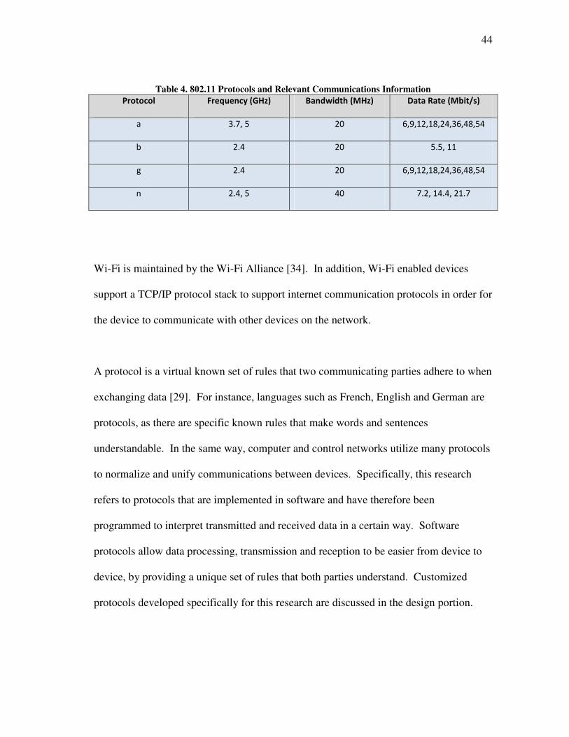
802.11x standard, where x stands for a version of the standard protocol. Available
standards and their frequencies are shown in Table 4 [34].
Page 60
44
Table 4. 802.11 Protocols and Relevant Communications Information
Protocol Frequency (GHz) Bandwidth (MHz) Data Rate (Mbit/s)
a 3.7, 5 20 6,9,12,18,24,36,48,54
b 2.4 20 5.5, 11
g 2.4 20 6,9,12,18,24,36,48,54
n 2.4, 5 40 7.2, 14.4, 21.7
Wi-Fi is maintained by the Wi-Fi Alliance [34]. In addition, Wi-Fi enabled devices
support a TCP/IP protocol stack to support internet communication protocols in order for
the device to communicate with other devices on the network.
A protocol is a virtual known set of rules that two communicating parties adhere to when
exchanging data [29]. For instance, languages such as French, English and German are
protocols, as there are specific known rules that make words and sentences
understandable. In the same way, computer and control networks utilize many protocols
to normalize and unify communications between devices. Specifically, this research
refers to protocols that are implemented in software and have therefore been
programmed to interpret transmitted and received data in a certain way. Software
protocols allow data processing, transmission and reception to be easier from device to
device, by providing a unique set of rules that both parties understand. Customized
protocols developed specifically for this research are discussed in the design portion.
Page 61
45
To allow computing devices to communicate with one another across a network, a
physical connection medium exists to allow data transfer coupled to a virtual connection
medium called a socket. Creating a socket is necessary for communicating endpoints in
this research that use both Bluetooth and Wi-Fi connection mechanisms because once
data is physically transmitted and received by two endpoints, the devices must buffer the
data, and determine to which application the data belongs. Creation of a socket is
handled by the operating system and is implemented through an Application
Programming Interface or API. To successfully create a socket, there must be both a
server and a client active in a communications medium. The server decides to open a
socket to listen for information while also creating a receiving buffer to store data
packets as they are sent from the client, and a transmitting buffer, in case data packets
need to be sent back to the client. Internet sockets on computers are then assigned or
complete a “bind” action to a virtual port or connection, to listen for incoming data [28].
Port values range from hexadecimal numbers 0x0000 to 0xFFFF. If the port has not
been occupied by another program, the server application is ready to receive data from
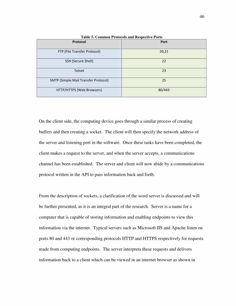
the client and is deemed to be “listening”. Table 5 lists some reserved ports for internet
protocols [28].
Page 62
46
Table 5. Common Protocols and Respective Ports
Protocol Port
FTP (File Transfer Protocol) 20,21
SSH (Secure Shell) 22
Telnet 23
SMTP (Simple Mail Transfer Protocol) 25
HTTP/HTTPS (Web Browsers) 80/443
On the client side, the computing device goes through a similar process of creating
buffers and then creating a socket. The client will then specify the network address of
the server and listening port in the software. Once these tasks have been completed, the
client makes a request to the server, and when the server accepts, a communications
channel has been established. The server and client will now abide by a communications
protocol written in the API to pass information back and forth.
From the description of sockets, a clarification of the word server is discussed and will
be further presented, as it is an integral part of the research. Server is a name for a
computer that is capable of storing information and enabling endpoints to view this
information via the internet. Typical servers such as Microsoft IIS and Apache listen on
ports 80 and 443 or corresponding protocols HTTP and HTTPS respectively for requests
made from computing endpoints. The server interprets these requests and delivers
information back to a client which can be viewed in an internet browser as shown in
Page 63
47
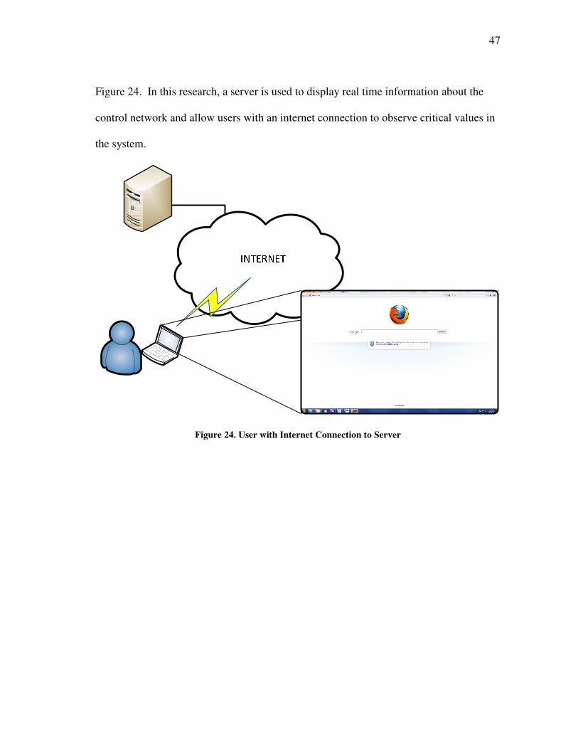
Figure 24. In this research, a server is used to display real time information about the
control network and allow users with an internet connection to observe critical values in
the system.
Figure 24. User with Internet Connection to Server
Page 64
48
CHAPTER IV
SYSTEM DESIGN
4.1 Array design
This project utilizes the background aforementioned to design and fabricate a four by
four microstrip patch antenna array. The process includes designing a single microstrip
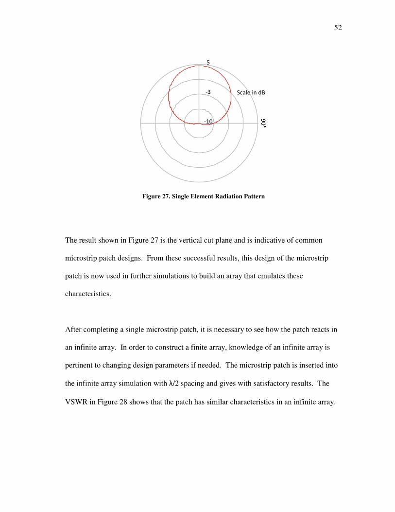
patch. A sufficient single model of a microstrip patch will have similar characteristics
when placed in an array. Next, simulate the single patch in an infinite array association
to observe how the patch will respond when surrounded by other similar patches. Last,
design a four by four finite array model that includes cross coupling among the patches
and other losses. It is from the final design that the physical array is constructed.
Throughout this process, the analytical use of the simulation tool will help to improve
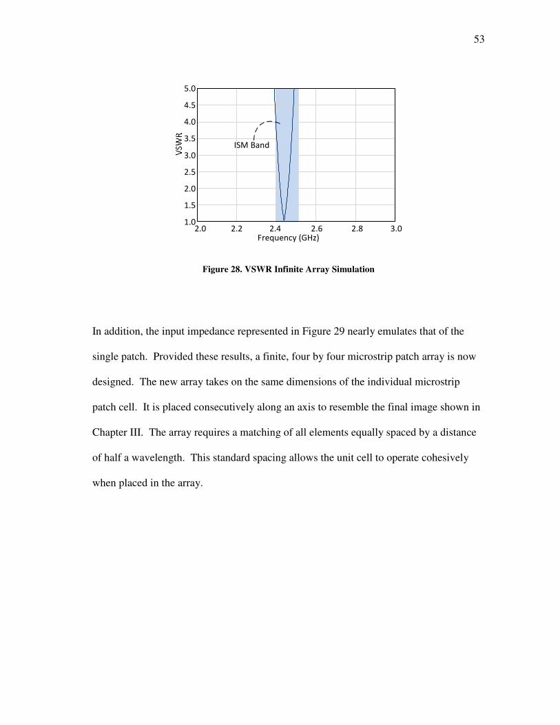
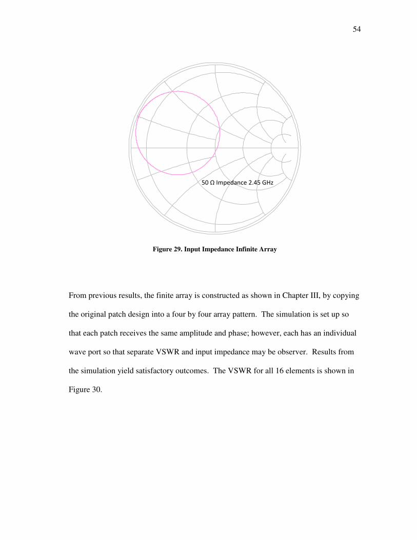
the design as observations of VSWR, input impedance and resonant frequency can be
tweaked to improve the overall design.
To begin, the design of a microstrip patch is straightforward. From (0.13) and (0.14) we
can determine the dimensions of the microstrip patch. For this design, the microstrip
patch is going to use Rogers 5880. The characteristics are shown from Table 6 [35].
Page 65
49
Table 6. Design Characteristics for Antenna Dielectric
Duroid εr Thickness
Rogers 5880 2.2 .787 mm
The project desires a resonant frequency of fr = 2.44 GHz. Using the values from Table
6, the width and length are determined to be
48 , 40 , 7initial initial
W mm L mm d mm= = = (0.23)
Numerical analysis for probe placement can be done using the cavity model [18];
however, for this project, the probe placement relies on analytical analysis from the
results of software. After simulating these dimensions, the results were not satisfactory.
Using knowledge of probe placement effect on input impedance and an adjustment of
width and length to a near unity ratio, a satisfactory simulation is achieved. The final
dimensions of the microstrip patch are represented from (0.24).
39.75 , 40 , 5.75final final final
W mm L mm d mm= = = (0.24)
From these dimensions we achieve the following VSWR and input impedance results.
Page 66
50
2.0 2.2 2.4 2.6 2.8 3.01.0
1.5
2.0
2.5
3.0
3.5
4.0
4.5
5.0
Frequency (GHz)
ISM Band
Figure 25. VSWR for Single Patch Antenna
From Figure 25, it is clear that the VSWR is below 1.10 for a frequency of fr=2.45 GHz.
This is satisfactory for design standards as we note that a perfect VSWR would be
exactly 1.0. The VSWR provides an indication for the standing wave ratio between the
incident and reflected voltages. In addition, the input impedance at our resonant
frequency is near 50 Ohms shown in Figure 26.
Page 67
51
50 Ω Impedance 2.45 GHz
Figure 26. Input Impedance Single Patch Antenna
It is necessary to look at the single element beam pattern to determine possible beam
patterns for the entire array. In addition, from the theory discussed in Chapter III, the
single element beam pattern multiplied by the array factor will provide the array pattern.
The beam pattern will also provide information of estimated maximum scan angles and
any radiation anomalies that may occur.
Page 68
52
-10
-3
5
Scale in dB
Figure 27. Single Element Radiation Pattern
The result shown in Figure 27 is the vertical cut plane and is indicative of common
microstrip patch designs. From these successful results, this design of the microstrip
patch is now used in further simulations to build an array that emulates these
characteristics.
After completing a single microstrip patch, it is necessary to see how the patch reacts in
an infinite array. In order to construct a finite array, knowledge of an infinite array is
pertinent to changing design parameters if needed. The microstrip patch is inserted into
the infinite array simulation with λ/2 spacing and gives with satisfactory results. The
VSWR in Figure 28 shows that the patch has similar characteristics in an infinite array.
Page 69
53
2.0 2.2 2.4 2.6 2.8 3.01.0
1.5
2.0
2.5
3.0
3.5
4.0
4.5
5.0
Frequency (GHz)
ISM Band
Figure 28. VSWR Infinite Array Simulation
In addition, the input impedance represented in Figure 29 nearly emulates that of the
single patch. Provided these results, a finite, four by four microstrip patch array is now
designed. The new array takes on the same dimensions of the individual microstrip
patch cell. It is placed consecutively along an axis to resemble the final image shown in
Chapter III. The array requires a matching of all elements equally spaced by a distance
of half a wavelength. This standard spacing allows the unit cell to operate cohesively
when placed in the array.
Page 70
54
50 Ω Impedance 2.45 GHz
Figure 29. Input Impedance Infinite Array
From previous results, the finite array is constructed as shown in Chapter III, by copying
the original patch design into a four by four array pattern. The simulation is set up so
that each patch receives the same amplitude and phase; however, each has an individual
wave port so that separate VSWR and input impedance may be observer. Results from
the simulation yield satisfactory outcomes. The VSWR for all 16 elements is shown in
Figure 30.
Page 71
55
Frequency (GHz)2.0 2.2 2.4 2.6 2.8 3.0
1.0
1.5
2.0
2.5
3.0
3.5
4.0
4.5
5.0
ISM Band
Figure 30. VSWR Finite 16 Element Microstrip Patch Array
Notably, the VSWR for all elements nearly overlaps one another and is contained within
the ISM frequency band having a resonant frequency of fr=2.45 GHz. We note that the
many elements share a similar VSWR which indicates a similar response among the
connected unit cells. In addition, observation of the smith chart in Figure 31 yields that
while some variance of input impedance exists between the elements; the general input
impedance is near the 50 Ohms design criterion. Some variation exists due the
proximity of the elements to one another, however; we have considered to neglect these
effects in this research.
Page 72
56
Figure 31. Input Impedance Finite 16 Element Microstrip Patch Array
Provided these results, it is sufficient that a formidable array model for this project is
complete. This model will be used in fabrication and final testing presented in the
experiments and results section.
4.2 Control design
This research incorporates many aspects of electrical engineering, coupling systems and
control with electromagnetics and antennas. Programming and mathematical algorithms
comprise network control theory while a system of digital logic and analog circuitry
provide the necessary hardware implementation to generate control voltages for phase
shifters. Bringing together different components requires an astute understanding of
Page 73
57
how data flows from one point of the system to another while interfacing many inputs
such as phone control or GPS. Therefore, this section of design covers general network
operation followed by a detailed account of data algorithms at a system level.
Functionally, the network has many states of operation that are possible through
dynamic programming in the phone. This centers the phone as the primary tool of
operation for both control and data generation. With this functionality, it is imperative
that the phone establish connections with two other components that will implement
physical control of the system and analyze data for system operability and observation.
One connection exists using Wi-Fi where the phone connects to a remote server using a
TCP/IP implementation of data exchange. This is under the assumption that the smart
phone is within range of either an access point or a 3G-4G connection and the server is
at an accessible IP address. Data exchanged between the phone and server consists of
the current yaw, pitch and roll information of the smart phone, the progressive phase
shifts for all antenna elements, system power usage information and object position, if
the phone is in tracking mode. This exchange of information allows information of the
system to be remotely gathered in near real time. In addition to the server connection,
the phone connects to an Arduino BT via Bluetooth, which allows for full-duplex
communication between the phone and phase shifter control circuitry. Through this
connection, the phone passes only the progressive phase shift information for antenna
elements, as this information is used by algorithms on the microcontrollers to control
phase shifters. In the opposite direction, data from the Arduino BT consists of system
Page 74
58
power usage information, and when necessary, system operating state information that
will be discussed shortly. These two connections sustain the entire system and allow
both the control and operation of the system to succeed; whereas, without these
connections and exchange of data, the system would not be able to operate.
^o ˁ
Object
Antenna
Array
Voltage
Control
Microcontrollers
(I2C)
Smartphone
Bluetooth
WI-FI
Server
Figure 32. General Network Overview
Figure 33. Network Overview with Physical Implementation
Page 75
59
Figure 32 provides a graphical overview of individual network components from a high
level, whereas; Figure 33 shows the physical depiction of each individual network
element including microcontrollers, power divider, PCB control board and antenna
array. As aforementioned, because of many system components it is necessary to use a
divide and conquer approach to designing all components, especially data flow and
algorithms.
The system operates in three different states which conduct what algorithms should be
run at the system and sub-system levels. The first mode of operation is defined as
“Manual User Control”. In this mode, the phone’s face, when calibrated coplanar with
the face of the antenna array, will determine the direction of the main beam of the
phased antenna array as shown in Figure 34.
Figure 34. Manual Tracking Mode of Operation
Page 76
60
The system algorithm differs from the other states primarily within the smart phone’s
algorithm itself. The algorithm pseudo code is shown in Figure 35 and the explanation
is as follows. The user accesses the smart phone and establishes two connections: one
with the server via Wi-Fi and one with the Arduino BT via Bluetooth. Once connected,
the user calibrates the phone coplanar with the radiating face of the phased array, and
establishes the appropriate broadside radiating direction. Next, the user generates yaw,
pitch and roll information from the phone by interacting with the program’s interface.
However, from the broadside direction, the phone generates phase shifts according to the
movement of yaw, pitch and roll information, not based on an object’s position in space
as this feature is included in other operating states. Upon generating progressive phase
shifts, the information is dispersed to the server and Arduino BT whereby the
microcontrollers interact with the control circuitry to produce a control voltage and
respective phase shift among all antenna elements. Gathering state information such as
power usage is optional in this operating state.
Page 77
61
Manual User Control Algorithm
Start
Initialize
Bluetooth,
Wi-Fi
Psuedo Code
Wait_for_bluetooth();
Wait_for_Wi_Fi();
Prompt_user_calibration();
If(Calibrated)
Wait_for_user_start();
Else
Prompt_user_calibration();
//gather data and determine
main lobe location
If(accel_started())
Read_orientation_data();
Rot_broadside_matrix();
Get_new_broadside_loc();
Calc_xy_phase_shifts();
Prepare_packet(B_x,B_y);
Accel_started();
//once packet sent, return
to check accelerometer
state
Else
Wait_for_user_start();
Prepare_packet(x,y)
Array = []
Array[payload] = x,y;
Send_packet(&array);
Send_packet(array)
Bluetooth.socket.send(array
);
Wi_fi.socket.send(array);
Return 1;
//sent to server and slave
circuit
Connected
Calibrate User
Position,
begin Data
Read
Yes
No
Phone
Movement
(Δx,Δy,Δz)
move
broadside
radiation
Calculate
Beta_X,
Beta_Y
Prepare
Packet
Send Packet
to Slaves
User Quit
Save State
(Icicle),
Exit
Yes
No
Figure 35. Manual User Control Algorithm System Level
Page 78
62
The second mode of operation is defined as “Manual Object Tracking”. As the name
implies, the phone’s algorithm focuses the main beam of the array at a particular point in
space, rather than allowing a user to manually control the direction of the beam. The
term ‘manual’ in this case refers to the system using the smart phone’s tilt information to
generate progressive phase shifts that track the object instead of the tilt information from
the accelerometer and gyroscope that are physically mounted to the array. This mode of
operation may be used in a case where a soldier desires to calibrate their phone with an
antenna array to track an object in space, but as they move the antenna tilts and does not
stay focused on the object. Thus, the movement of the smart phone would resemble the
movement of the array itself and therefore, the tilt information can be used to generate
phase shifts to allow the beam to track the object.
Figure 36. Manual Object Tracking Physical Representation
Page 79
63
The system algorithm as shown in Figure 37, differs slightly from ‘Manual User
Control’ in that the phone’s tilt information is now used to shift a point in space using
(0.21). Corresponding phase shifts are generated from the transformed Phi and Theta
and are then used in microcontroller and voltage control circuits similarly to “Manual
User Control”. Here, the internal sensors of the phone are used to the greatest extent to
over compensate for the physical systems movement. The overall algorithm doesn’t
change with its processes, however; it is indicitavely the math that changes so as to
produce correct results in the system. Similar correspondences are made between these
two algorithms, however; the purpose of the second algorithm is used in an object
tracking sense, whereas, the manual user control more demonstrates a proof of concept.
It is noted that the method of object tracking in this algorithm is very simple in design.
It uses the coordinates of two objects in space to determine the distance and angles in a
respective coordinate system. It then assumes that the refresh rate of the system is faster
than the objects speed; whereas, other algorithms discussed in Chapter II apply historical
data to estimate an object’s future position.
Page 80
64
Manual User Object Tracking
Start
Initialize
Bluetooth,
Wi-Fi
Psuedo Code
Wait_for_bluetooth();
Wait_for_Wi_Fi();
Prompt_user_calibration();
If(Calibrated)
Wait_for_user_start();
Else
Prompt_user_calibration();
//gather data and determine
point location
If(accel_started())
Read_orientation_data();
Rot_3D_point_matrix();
Get_new_point_loc();
Calc_xy_phase_shifts();
Prepare_packet(B_x,B_y);
Accel_started();
//once packet sent, return
to check accelerometer
state
Else
Wait_for_user_start();
Prepare_packet(x,y)
Array = []
Array[payload] = x,y;
Send_packet(&array);
Send_packet(array)
Bluetooth.socket.send(array
);
Wi_fi.socket.send(array);
Return 1;
//sent to server and slave
circuit
Connected
Calibrate User
Position,
begin Data
Read
Yes
No
Phone
Movement
(Δx,Δy,Δz) 3D
tracking point
Calculate
Beta_X,
Beta_Y
Prepare
Packet
Send Packet
to Slaves
User Quit
Save State
(Icicle),
Exit
Yes
No
Figure 37. Manual Object Tracking Algorithm and Pseudo Code
Page 81
65
The third mode of operation is defined as “Autonomous Object Tracking”. This system
level algorithm is similar to ‘Manual Object Tracking’ with the difference that the tilt
information to track an object is generated from an accelerometer and gyroscope on the
antenna array; however, the calculation to track an object using tilt information is still
performed on the phone. The system algorithm is similar to the first two with the
aforementioned difference of generated tilt information. In this case, the smart phone
must wait for generated tilt information from the Arduino BT via the Bluetooth
connection. Because there is a specific protocol that does this, error checking and delay
cause this system algorithm to be slightly slower than the first two. Gathering the tilt
information is discussed in the Arduino BT algorithm design. Upon receiving the tilt
information from the Arduino BT, the smart phone performs the same algorithm as the
‘Manual Object Tracking’ case, then sends phase shift information back to the Arduino
BT and control circuitry.
P
(Δx, Δy, Δz)
Beam Tracking, Array SensingCalibrate
Broadside
Figure 38. Autonomous Array Object Tracking
Page 82
66
Autonomous Object Tracking
Start
Initialize
Bluetooth,
Wi-Fi
Psuedo Code
Wait_for_bluetooth();
Wait_for_Wi_Fi();
Prompt_user_calibration();
If(Calibrated)
Wait_for_user_start();
Else
Prompt_user_calibration();
//gather data and determine
point location
If(accel_started())
Rd_orient_arraysensor();
Rot_3D_point_matrix();
Get_new_point_loc();
Calc_xy_phase_shifts();
Prepare_packet(B_x,B_y);
Accel_started();
//once packet sent, return
to check accelerometer
state
Else
Wait_for_user_start();
Prepare_packet(x,y)
Array = []
Array[payload] = x,y;
Send_packet(&array);
Send_packet(array)
Bluetooth.socket.send(array
);
Wi_fi.socket.send(array);
Return 1;
//sent to server and slave
circuit
Connected
Calibrate User
Position
Yes
No
Read Array
Orientation
Sensor via BT
(Δx,Δy,Δz) 3D
tracking point
Calculate
Beta_X,
Beta_Y
Prepare
Packet
Send Packet
to Slaves
User Quit
Save State
(Icicle),
Exit
Yes
No
Figure 39. Autonomous Object Tracking Algorithm and Pseudo Code
Page 83
67
The simulations and results presented in this research focus on the system level
algorithm “Manual User Control” as this demonstrates the broadest proof of concept and
satisfies the original requirement of the project. The latter algorithms present the
dynamic programming ability of the smart phone and other possible states of operation
of the overall system.
4.3 Circuit design
The algorithm on the phone determines system clock synchronization, tilt information
for beam control and handles data communication between the control network and
server. From the block diagrams in Figure 35, Figure 37, and Figure 39 it is clear that
the phone algorithm has multiple threads that execute asynchronously to meet the
demands of different system components. Upon opening the application, the phone
establishes a Bluetooth connection by default to the Arduino BT microcontroller. This
assumes the MAC of the Arduino BT is known. It also begins reading data from the
orientation sensor in the phone after calibration. If desired, the user may input the IP
address of the server to send network information, assuming that a server’s IP address
resides on a reachable subnet and that the server listens on a socket. The user must now
calibrate the position of the phone to the desired calibration location of the array. Most
often, the user calibrates the phone coplanar with the array to calibrate the default
position at broadside. The phone data algorithm begins if the user presses the start
button on the screen. Data is read from the orientation sensor to determine the angular
shift from the calibrated positions along the x, y, and z axis. This data is sent to the
Page 84
68
function which performs the rotation matrix calculation. Analysis of the current system
operation algorithm i.e.(Manual User Control, Manual Object Tracking, Autonomous
Object Tracking) determines which rotation matrix is used. Note that the user has
instantaneous access through the phone’s interface to change the system operation mode
as discussed in earlier in this section. New primary θ and φ locations are generated and
the respective phase shifts are put into an array. The phone creates a packet using the
correct protocol and sends the phase shift information to the Arduino BT. This process
is illustrated in Figure 40.
Figure 40. Pseudo Code Phone Algorithm Calculating Point
Under a separate thread, the phone actively listens for information from the Arduino BT
to send to the server. The information received references a different protocol when
received in the buffer. Data is stripped from the packet and stored in an array. If the
Page 85
69
phone is connected to the server, it will read the array and store the data in a packet to be
sent to the server.
The algorithm run on the Arduino BT for protocol communications varies dependent on
system operation state. The general implementation is as follows. The packet is
received at the Arduino BT RFCOMM port and is stored in a buffer. An algorithm runs
on the Arduino BT that determines slaves connected to the I2C bus, send phase shift data
to slaves and read network information such as tilt values from the onboard
accelerometer. As shown in Figure 41, the Arduino BT reads the RFCOMM buffer and
parses the packet based on protocol information. It determines which slaves are
listening to the I2C network and forwards the packet if the checksum of the packet is
correct. If the checksum is not correct, the Arduino BT drops the packet and waits for
the next packet of data from the phone implementing a UDP style communication. After
the packet is sent to the slaves, the Arduino BT reads network information, creates a
packet and sends the information to the phone. This process repeats with each packet
that is received into the RFCOMM buffer; therefore, it is the rate at which the phone
sends information that determines the rate for the Master-Slave I2C network to process
information.
Page 86
70
Bluetooth Microcontroller Algorithm
Start
Wait For
Bluetooth
Connection
and Initialize
Psuedo Code
Initialize_Outputs();
Wait_for_bluetooth();
//make sure we’re
connected
Wait_for_startbyte();
If(startbyte)
If(!checksum)
Return;
else
Store_packet(*packet);
//temporary store before
sending to slaves
Check_slaves();
Send_packet_to_slaves();
Read_acceleromter();
Store_accel_data();
//depends on system
operation state
//read power usage
Store_power_usage();
Send_data_to_phone();
Endif
Else
Wait_for_startbyte();
Connected
Wait For
Startbyte
Checksum
Correct
Store Packet
Slaves on
Network
Forward
Packet to
Slaves
Read Network
Info send to
phone
Return
Yes
Yes
Yes
No
No
Figure 41. Arduino Bluetooth Master Control Algorithm
Page 87
71
The data is received by the slaves as the same packet that was received by the Arduino
BT under the checksum condition. The checksum is checked again. If the checksum is
valid, the phase shift values are used in the algorithm to generate a phase shift voltage,
however; if invalid, the slave waits for the next packet to arrive. This algorithm analyzes
the signs of the phase shifts, as different signs on the phase shifts indicate θ and φ in
various quadrants as viewed in Table 7.
Table 7. Phase Shift Signs for Quadrants of X-Y Coordinate System
Quadrant Phase X Phase Y
I - -
II + -
III + +
IV - +
Figure 42. Main Beam Location in Various Cartesian Quadrants
Page 88
72
Each slave is responsible for generating voltage values for 8 individual phase shifters.
From the analysis of the phase shifters in Chapter III, (0.16) relates an input phase shift
to a respective output voltage. The phase shifts are calculated for the respective
elements which produce a corresponding voltage. The voltage is related to an 8-bit word
that the potentiometer uses to adjust the wiper position between 0 and 5 Volts. The
digital word is placed in an array to be delivered to the SPI network control circuitry.
Once the correct 8-bit word is stored in the array, the slave activates the SPI network by
addressing the de-multiplexor with an activate signal referenced in Table 2. The de-
multiplexor from section 2, is inactive until this signal arrives from the slave. Next, the
slave uses two digital outputs, A and B, to address the appropriate digital potentiometer
according to Table 2. The de-multiplexor receives signals A and B and activates a
digital potentiometer as seen in Figure 43.
Page 89
73
Figure 43. De-Multiplexor with Digital Potentiometer
The slave now uses the SCLK and the MOSI line to communicate the respective 8-bit
word to the digital potentiometer. The word is stored in ROM on the digital
potentiometer and accordingly produces a voltage on the wiper pin of the digital
potentiometer that is sent to a non-inverting operational amplifier configuration. A static
gain is configured by adjusting the values of the resistors according to (0.22). Whereas,
the voltages produced by the digital potentiometers range from 0 to 5 Volts, the static
gain provided by the operational amplifiers provides a range from 0 to 12 Volts, which
the phase shifter requires for full 360 degree phase shift capability. The SPI algorithm is
highlighted in Figure 44 and the data flow from slave to output voltage is seen in Figure
45.
Page 90
74
SPI Algorithm (Slave Microcontrollers)
Start
Listen For
Startbyte I2C
Packet
Checksum
Correct?
Normalize
Array Values
Map Delays to
Phase Shifter
Voltage
Map Phase
Shifter
Voltage to
Digital Word
Write Digital
Word to
Respective
Potentiometer
Repeat
Psuedo Code
Initialize_Outputs();
//Set pins to no-write
mode on demux
Listen_I2C_Port();
If(startbyte == packet[0]))
Store_packet(*packet);
//we want to store all
data
//packet length variable
Quadrant(*payload);
//quadrant determines
which quadrant to
implement phase shifts
Int PhaseX = payload[0];
Int PhaseY = payload[1];
Calc_phase_each_patch(
PhaseX,PhaseY);
//determine phases
Int *phases[8];
//store 8 phases
Calc_voltage(phases);
Int *voltages[8];
Calc_words(voltages);
Write_words(all_pots);
Endif
Else
Wait for next packet();
Yes
No
Figure 44. SPI Algorithm Implemented on Arduino Uno
Page 91
75
Figure 45. Microcontroller Writing Process to Digital Potentiometer
In addition, the SPI algorithm implements extended mathematical calculations that
weren’t previously covered in the background section. Because the system is using
general phase delay and not true time delay, the phase differences for all elements must
be normalized to one another. In other words, the maximum phase difference for any
element is 360 degrees while the minimum for any element is 0 degrees. This means
that for negative degree phase shifts and phase shifts which exceed 360 degrees require
some scaling in reference to other elements. When the algorithm checks the sign of the
phase shift, it determines the element which has the greatest positive phase shift and the
least negative phase shift. To have all phase shifts negative, the algorithm subtracts the
Page 92
76
greatest positive phase shift to all element calculations as this normalizes the starting
value to 0. Each phase shift is now calculated with respect to the normalized value.
Furthermore, the SPI algorithm must find an appropriate digital word to write based on a
calculated voltage. In this system, there are 127 possible voltages that may be achieved
from 0 to 12 Volts or each digital potentiometer voltage step size is approximately .04
Volts. The algorithm finds the best match with the calculated voltage rounding the
number if it is not an integer. This number corresponds to a wiper position which is the
number in binary format that is written to the digital potentiometer.
The voltage control circuitry is designed to be modular to the entire system. Its specific
function is to react to control signals from the microcontrollers and produce output
voltages. In addition, it has the ability to link many separate system sub-components
together. With this in mind, it is pertinent to design a printed circuit board (PCB) in
order to organize system components, and provide a natural structure for control
circuitry elements. In the same way that the voltage control logic was designed, the
schematics for the system were designed at sub levels, instantiated with each layer of
hierarchy. The first layer is the digital potentiometer and de-multiplexor layer.
Page 93
77
Figure 46. Digital Potentiometers and De-multiplexor Stage
Figure 47. Operational Amplifier Stage, 8 Op-Amps Shown
Page 94
78
From Figure 46, one can see the de-multiplexor in the upper left with 16 inputs and 8
digital potentiometers on the right. Next, an op-amp stage is created to take the outputs
from the digital potentiometers and amplify the voltage from 0 to 12 Volts.
From Figure 47, one can see the combination of resistors that produce the static gain. At
the next level of hierarchy, these are combinational logic blocks. The top layer, as
shown in Figure 48, provides access to these blocks; in addition, to the other needed
electrical connections at this layer such as external I2C and power connections. This top
level also has copper traces that extend to the edge of the board where SMA connectors
will bring the DC voltage to the respective phase shifter. There are 8 SMA connectors
on the right and left sides of the board corresponding to phase shifters 1-8 on the right
and 9-16 on the left.
Figure 48. Final PCB Design (Top Layer) Schematic (Left) 3-D Representation (Right)
Page 95
79
The external pin connectors allow both Arduino Uno slaves to be connected via a 14 pin
connector cable. The I2C and power connectors are connected with a 10 pin connector.
From Figure 48, one can see that in the middle exist two ICs. These are two separate de-
multiplexors. On both sides, extending from the middle, exist 4 ICs in a straight line.
These 4 ICs comprise 8 total digital potentiometers. Furthermore, 4 additional ICs exist
at each corner. These contain 4 op-amps. This final design of the PCB allows the
systems sub components to come together in a modular fashion and in addition, provide
a convenient way to connect many ICs together.
4.4 Communications design
The algorithms that process the data generated by the phone, network and user
ultimately provide the functionality for the control system; however, without
communication between device peripherals, control would not be possible. Therefore, it
is necessary to provide a unified communications scheme between devices to help
simplify the overall network design and to establish a layered approach to inter-device
communication as discussed in section 2. Accordingly, custom protocols are designed
specifically for this project to achieve the aforementioned objectives; in addition to,
providing increased communications efficiency and improving network operability.
Naturally, the most important protocol of the system is that which determines the
communications standard between the phone and control circuitry. Each packet sent
from the phone carries phase shift information, but it may carry other information under
Page 96
80
various system operations. The length of the packet is variable because of the payload
information, thus; a protocol is designed to fit these needs. The protocol states that the
first byte of a packet is classified as a start byte. The start byte is an 8 bit integer that the
device recognizes as the beginning of a packet. In this case, packets sent from the phone
to the control circuitry start with the number 255. Next, the receiving device needs to
allocate memory to store the payload, therefore; a length byte is included which is an 8-
bit integer signifying a count of the number of bytes after it. Because the system may
have a variable length packet, dynamic memory allocation is very important on the slave
devices. Because the system may have various operation modes, all which require
different payload data, a frame type byte is included that informs the sender and receiver
what type of information is sent. In this case, when phase shift data is sent, the sender
inserts a 200 to signify that the payload is phase shift data. In addition, if TCP
communication is desired, the packet must have a frame id byte for SYN and ACK to be
accurate. This is included after the frame type. The payload, or data being sent, is the
remaining bytes inserted into the packet. A checksum byte to ensure data integrity is the
last byte in the packet and is calculated by
( )%6Checksum startbyte lengthbyte type payload= + + + (0.25)
Therefore, the receiver and subsequent receiving stages can compute a checksum using
(0.25) and compare to the original checksum to ensure data integrity. The evaluation of
checksums in the algorithms is discussed in Chapter 3.4.
Page 97
81
Figure 49. System Wide Protocol Packet Structure
While a protocol exists to send information from the phone to the control circuitry, a
similar protocol is instantiated for the control circuitry, mainly the Arduino BT, to
communicate information to the phone. The packets utilize a start byte, length byte and
frame id; however, a different frame type is used for the payload information. In one
case, the Arduino BT sends accelerometer information from an onboard sensor back to
the phone. This type of information utilizes a frame type byte of 201. In another case,
the Arduino BT captures power usage of the system by reading a sensor and
communicates this usage with a frame type of 202. It is important that the protocol is
similar in both directions as to not use substantial programming overhead.
Communication also exists between the phone and network server, relaying information
about system operation, power usage and other peripherals. A similar protocol is
established to pass information from the phone to the server which is processed by the
server before displaying to a web page. The server resides on an IP address and opens
port 4444 to listen for data from the phone. Similarly to the circuitry protocol, the phone
to server protocol uses a start byte, length byte and frame id, although UDP is used in the
project. The frame type changes with each variation in payload that is sent from the
phone to the server. To update users of the system’s operational state, the phone
Page 98
82
communicates phase shift information to the server using frame type 200. For power
readings, the phone inserts frame type 202 into the packet.
The protocol for communication between the server and the phone is implemented in
software on a continuously running thread which updates a web page. Using an HTTP
browser, a user from the internet may remotely see system information in real time by
observing the display of information. This display updates the user of current phase
shifts, beam direction, system operational state and power usage. Although not vital to
system operation or control, the information gathered by the server provides details that
are important for real world implementation. Reading and trending power usage may
indicate when system circuitry components are wearing down or observing phase
information can inform a user how the system is performing in tracking an object. In
addition, a real time display of information pertinent to the system expands ideas on how
to better improve the system and design system components for improved efficiency.
4.5 Phone and server display design
Accurately showing data and visually appealing graphics, while not completely
necessary to this project, enhance the results and usability of this project as a whole.
The partial goal of using a smart phone in this system is to allow a user to integrate
easily into an otherwise, complex radio system. With this in mind, the design of the
phone interface is somewhat important. The design allows the user to take advantage of
the aforementioned dynamic programming capability of the phone. In addition, it is
Page 99
83
necessary to observe the phase shifts and angular values that the system is using for
calculations. This ensures system operation is correct from a user standpoint.
Because the phone has many threads running concurrently, it is difficult to fully display
all of them synchronously; however, separate visual designs still offers advantages to the
system. In this design, the primary viewing screen of the phone displays important
information including: θ and φ values, generated phase shifts from these angles,
operation state and operable buttons whose functions control internal flags within the
phone’s algorithm. These criterions allow the user to fully observe the system state and
important information from the screen as this is especially useful if the user is
controlling the direction of the beam with “Manual User Control”. In addition to the
primary screen, the user needs the option to connect to a server for to transfer
information; however, this need not be displayed continuously. A separate screen is
created to input the IP address and accordingly, display server connection information.
The Bluetooth is managed by a separate library called “Amarino”, which runs as its own
process in the background of the phone. An initial screen design is shown in Figure 50.
Page 100
84
Figure 50. Initial Phone Design
Because the phone communicates with the server, it too should also display pertinent
system level information to provide remote users an insight into system operation.
Remote users have access to phase shift information, the main beam’s current location in
terms of θ and φ, individual phase shifts for each of the elements and historical
information of system operation state. While these features are no more necessary than a
visually appearing phone application, they can provide useful information to improve
future operation of the array. Power information is stored on the server which is
Page 101
85
analyzed to determine weak circuit components for replacements. Furthermore, visual
graphics provide non-technical users insight to antenna operation and other
characteristics of the system. With this in mind, the server display offers a chance for
others to develop new innovative ideas that can be included in the research and progress
the development of this project.
Figure 51. Initial Server Display Design
Page 102
86
CHAPTER V
COMPLETED DESIGN AND RESULTS
5.1 Completed design
This section presents the completed physical models of all designed sub-components
including the phased antenna array, power divider, phase shifter, voltage control board,
phone display and server display. Results are presented which correspond to simulated
results in Chapter IV. Overall system experimental results are presented to show the
functionality of the system as a whole and its success steering the beam of the array.
The finite array simulated in Chapter IV is etched on a 10 by 10 inch slab of Rogers
5880. From Figure 52, it is clear that the design resembles the image of the simulated
array.
Figure 52. (Left) Fabricated Microstrip Patch Array (Right) Simulated Microstrip Patch Array
Page 103
87
The array is tested with a network analyzer for several measurements. Individual
antenna elements are tested for VSWR characteristics that are compared to simulated
results. In addition, cross coupling noise is simulated among four patches to determine
any losses associated with the fabricated array. Furthermore, input impedance is
graphed on a smith chart to compare against simulated results. From Figure 53, it is
clear that the VSWR of the fabricated array emulates that of the simulation.
VS
WR
Figure 53. VSWR Fabricated Array
Each element has a VSWR less than 1.20 with a resonant frequency of fr=2.46 GHz,
which is close to the expected model. It is also noted, that the VSWR for all elements
falls in the ISM band, which satisfies another design criterion. Observing the smith
chart in Figure 54, one can see that the input impedance of each element yields better
results the simulated design.
Page 104
88
Figure 54. Input Impedance Fabricated Array
-70
-60
-50
-40
-30
-20
-10
2.0 2.2 2.4 2.6 2.8 3.0Frequency (GHz)
Port 1
Patch 2
Patch 7
Patch 8
Figure 55. S21 Measurements 4x4 Array
Page 105
89
The impedance for all 16 elements at resonance varies by 2%. In addition, it is
important to observe the effects of neighboring patches, because many single elements
are electrically close. Because some energy may leave one patch but reradiate into
another, a test must be done to see how much energy dissipates from one patch to
another. From Figure 55, it is clear that little energy is absorbed by the neighboring
patches on the array. In addition, it is expected that Patch 2 will present the highest
coupling to Port 1. For these experiments, it is important that most of the energy radiate
from the patches to measure the radiation pattern accurately. Provided these test results,
the fabricated array adequately meets the needs of this experiment.
Upon completion and testing of the phased array, other RF hardware components are
now tested. The phase shifters are tested with the network analyzer using Labview to
determine the accuracy of an applied voltage to a corresponding phase output. The
Labview results of this experiment are shown in Figure 56.
Page 106
90
Figure 56. Graphical User Interface LabView for Hittite Phase Shifter Test
Ph
ase
Sh
ift
(De
gre
es)
Figure 57. Test Results from 16 Hittite Phase Shifters
Page 107
91
From the results in Figure 56, it is necessary to observe a similar graph as discussed in
Chapter IV to determine an appropriate equation to use in the SPI algorithm. Figure 57
follows closely with the original graph provided in the datasheet and the Hittite graph;
however, there exists some variation. Therefore, this variation must be accounted for in
the algorithm on the microcontrollers.
3 22 09*deg 3 05*deg 0.0118*deg .0816Voltage E E= − + − + − (0.26)
From Figure 57, there exists a noticeable change from the original voltage and degree
relationship equation. From this variation, a new equation (0.26) is created through the
same polynomial interpolation technique to map an input degree value deg, to a
respective output voltage. Furthermore, (0.26) requires the op-amp stages to have a gain
necessary to obtain all voltages. In reference to the op-amp feedback, the following
resistors are selected
2 115 , 7.3R k R k= = (Ω) (0.27)
These values provide a static gain of about 3. Thus, with the op-amps configured and a
new equation, the change is accounted for in the code implementing the SPI algorithm
on the slave microcontrollers explained in Chapter IV.
The control board was designed in Chapter IV using schematic and layout software.
These files are sent to a PCB manufacturer and returned for testing. The final outcome
of the board appears exactly as the simulated board. The board is shown in Figure 58
below.
Page 108
92
3D Preliminary Design Actual Fabrication
Figure 58. Simulated and Finished PCB
The microcontrollers are programmed with the necessary algorithms and are connected
to the control board for testing. In this experiment, the phone is calibrated into a
beginning position and then tilted to achieve some desired θ and φ. From this, we can
measure the voltage using a voltmeter and correlate these values to distinct phase shifts
measured by the lab view experiment. Two results are presented here.
Page 109
93
Table 8. First Experimental Result Beam Steering
Voltage Actual Phase Shift Actual Phi
Actual
Theta
1.094 84 42 46
2.79 170
4.84 249
7.33 333
10.72 423
7.66 344
6.32 302
2.91 172
5.28 265
7.88 350
11.05 440
2.9 172
5.28 265
3.12 184
1.32 96
8.24 360
Page 110
94
The voltages of all sixteen outputs are measured on the control board and are put into the
respective column. Thereafter, the corresponding measured phase shift is calculated and
inserted into the respective column. The phase shifts are entered into the simulation tool
to provide a radiation pattern as shown in Figure 59.
90
°
Ga
in (
dB
)
Figure 59.(Left) Polar Plot Experimental Results 45 Degree Cut Plane (Right) Rectangular Plot 45
Degree Cut Plane
The results shown indicate that the control board implements the voltage control
algorithm correctly and provides correct voltages to the phase shifters as a ϕ=44 and
θ=45 degrees is achieved. In addition, a second test is performed to ensure the algorithm
can move a beam into different Cartesian quadrants, satisfying the original three
dimensional beam steering requirement.
Page 111
95
Table 9. Second Experimental Result Beam Steering
Voltage Actual Phase Shift Actual Phi
Actual
Theta
8.1 356 307 42
5.29 265
2.91 172
1.09 84
2.44 151
4.71 245
8.38 364
10.81 427
2.45 152
10.02 407
6.86 318
4.26 227
6.28 299
9.33 389
2.1 136
4.27 228
Page 112
96
The results are displayed in Table 9 yield the following beam steering results shown in
Figure 60.
90
°
Ga
in (
dB
)
Figure 60. (Left) Polar Experimental Plot 135 Degree Cut Plane (Right) Rectangular Experimental
Plot 135 Degree Cut Plane Electric Field
A ϕ=-45 and θ=-45 degrees is achieved. These results satisfy the desired values held in
Table 9. It is clear from these results that beam steering in various Cartesian quadrants
is accurately achieved as both θ and φ are pointed nearly -45 degrees on the 135 degree
plane. These results yield promising outcomes for the system as a whole although the
physical array is not yet connected to the system and tested at this point.
Page 113
97
S1
X M
agn
itu
de (
dB
)
Figure 61. Power Divider Experimental S21 Gain Results
Ph
ase
(d
eg)
Figure 62. Power Divider Experimental S21 Phase Results
Page 114
98
As addressed in Chapter III, the power divider was tested for reliability using the
network analyzer. A measurement was taken to observe the S12 through S117 gain
parameters to ensure a similar gain distribution among the ports. From Figure 61, it is
clear that a .8 dB range exists among all the ports. These results signify little change
from port to port which will allow the overall system experiments to be performed with
greater accuracy. In addition, a measurement of phase difference for all ports is taken to
ensure that any phase differences are accounted for in the algorithm.
From Figure 62, observations conclude that the range of phases from port to port is
insignificant so as to not be an influence in the SPI phase shifting algorithm. In
conclusion, the measurements from the power divider signify that it does not play a
significant role in changing overall system state with respect to gain or phase.
The phone interface is designed to allow the user to have complete dynamic control of
the system. The interface for the primary screen is shown in Figure 63.
Page 115
99
Figure 63. Phone Executing Algorithm and Displaying Information
The screen has several parts. The calibration button is used to gain an initial condition
for the array; the system will not function without pushing this button first. Above the
calibrate button sits a start button, which begins reading data from the phone. Active
displays of phase shifts along with θ and φ are presented to show the user current beam
location information. Furthermore a switch is implemented as a checkbox which that
allows a user to change from “Manual User Control” to “Manual Object Tracking”. In a
Page 116
100
similar association, there is also a checkbox to enter “Autonomous Object Tracking”. A
second page, accessed by pressing the “Menu” button, leads a user to a form that
prompts entry of an IP address to connect to the server. Other important network
information is also displayed.
Figure 64. Server Communication Page
Other information can be displayed on the phone that is perhaps, important to the
phone’s or system’s algorithm. This is covered in Chapter VI under future work.
Information displayed on the server is also valuable as discussed in Chapter IV. The
design for the server displays system information such as 3-Dimensional beam location,
Page 117
101
phase shifts of elements and other characteristics. Network characteristics, such as
power usage, are stored in a database and can be accessed via web. The Apache server
is capable of responding to HTTP and HTTPS requests. The primary tool used to
construct the graphical interpretation of the beam was through a tool called “Processing”
and is written in Java.
Figure 65. Real Time Server Display of System Information
The server display in Figure 65 displays the directional cosine angles from the calibrated
axis shown as X,Y,Z and the progressive phase shifts are displayed as B_X,B_Y for the x
and y axes respectively. In addition, a color coded map of each antenna element displays
the progressive phase shift corresponding to the current data. The large object in the
Page 118
102
middle of the screen represents the beam of the array, and moves in real time
corresponding to the movement of the actual beam of the array.
5.2 Experimental results
With each sub-component fabricated and tested, the final experiment compiles all
modules into a single unit. Constructed from transparent acrylic glass, the final module
resembles a portable phased array.
Figure 66. Completed System Design
The completed module, shown in Figure 66, is tested in an anechoic chamber to observe
radiation pattern measurements in the presence of beam steering. The system sits on top
of a piece of wood. The power divider and phase shifter are secured into a piece of
Styrofoam and the cables to the phased array are secured with another piece of
Styrofoam. The control board lies in front of these pieces directly behind the phased
Page 119
103
array. For the measurements, all metal pieces are covered with absorber material to
decrease the reflections and measured noise. These measurements are compared to
those achieved by generating voltages and observing the simulation as recorded earlier
in this chapter.
The first measurement shown in Figure 67, is the radiation pattern of the array at
broadside radiation. This outcome corresponds strongly with the single element pattern
aforementioned in Chapter IV, however; it is strongly noted that the beam of the array is
thinner than that of the single element radiation pattern; this is expected.
-20
0
200°
Figure 67. Antenna Broadside Radiation Pattern
Given the outcome of the radiation pattern, several measurements were taken to obtain
the electric fields in both the θ and φ directions. Figure 69, shows the many scan angles
Page 120
104
taken in the measurement. The total scan ranges from -45 degrees to +45 degrees at 15
degree intervals. In these measurements, the anechoic chamber is capable of measuring
in a plane, not in three dimensions. Because of this, it is necessary to configure the
measurements such that the scan angles can be captured in the plane of radiation. With
each measurement, we program the phone to generate a phase shift that is coplanar
which generates a distinguishable measurable phase shift. In addition, we also program
the phone to take a perpendicular measurement to the radiation plane. In this
measurement, we see that the gain at broadside radiation drops because the beam is
steered off broadside. This is demonstrated in Figure 68.
HornArray
Capable of Measuring Angle
θ
HornArray
Maximum Radiation Drops at Broadside
Figure 68. Measurement Process Inside the Anechoic Chamber
Page 121
105
In the first series of measurements, we capture the electric fields with respective phase
shifts plotted in Figure 69.
-20
90
°
0
200°
Broadside
153045
-15-30-45
Gain
(d
B)
-70
-60
-50
-40
-30
-20
-10
0
10
20
Angle (deg)-150 -100 -50 0 50 100 150
Cross Pole Floor
Side Lobe Floor
Figure 69. (Left) Co-Planar Measured Electric Field in Phi Direction (Right) Measurement Fields
with Cross Pole
Clearly, the results achieved are closely related to those achieved in simulation. The
system demonstrates a successful capability to scan at angles within this range as each
measurement was taken according to the phase shifts generated from the phone. We
note that the drop in gain is around .3 dB with each progressive 15 degree phase shift. It
is also noted that the cross pole floor is low to the gain of the antenna which
demonstrates successful antenna operation.
Page 122
106
-20
90
°
0
200°
Broadside
153045
-15-30-45
Gain
(d
B)
-70
-60
-50
-40
-30
-20
-10
0
10
20
Angle (deg)-150 -100 -50 0 50 100 150
Side Lobe Floor
Cross Pole Floor
Figure 70. (Left) Normal Measured Electric Field in Phi Direction (Right) Measurement Fields with
Cross Pole
Figure 70 shows the measurement that is perpendicular to the measurement plane. We
see that the maximum radiation at broadside drops with each progressive 15 degree
phase shift. This signifies that the beam is steered away from the measurement plane by
the angle programmed from the phone. At a closer look, we view a discontinuity for the
-15 degree measurement. After analysis of the raw data, we conclude that this error is
due to a measurement error during the data gathering process. With proper review, we
apply the estimated measurement error to the raw data set and achieve Figure 70.
Page 123
107
90
°
Gain
(d
B)
Figure 71. Adjusted Data Set Due to Measurement Error
From Figure 71, we can see that after the measurement error adjustment, the
corresponding data provides an accurate result to proper array operation. As expected,
the -15 degree broadside beam is slightly less (1.5 dB) than the broadside beam. It is
also necessary to compare the measured results with the simulated results to determine
the accuracy and validity of the previous results.
Page 124
108
90
°
Figure 72. Simulated and Measured Comparison at +45 and -45 Degree Scan Angles
From Figure 72, we see that the measured results align closely with the simulated
results. This verifies our initial assessment of the system and confirms the previous tests
run on the modules in the system. Furthermore, the electric fields in the θ direction,
similar to those in the φ direction, are also shown below with the same measurement
process.
Figure 73. (Left) Co-Planar Measured Electric Fields Theta Direction (Right) Measured Fields with
Cross Pole
Page 125
109
These results are taken after the array has been physically turned to obtain the electric
field in a perpendicular direction. From Figure 73, we can see the beam shift is present
over the measurement range and the cross pole measurement also agrees with the
previous results.
Gain
(d
B)
90
°
Figure 74. (Left) Normal Measured Electric Fields Theta Direction (Right) Measured Fields with
Cross Pole
Again, the normal measurement indicates a drop in gain at broadside for the radiation
pattern. This result agrees with the other results and indicates successful system
operation.
Page 126
110
-20
0
20
SimulatedMeasured
0°
Figure 75. Simulated and Measured Comparison Electric Fields Theta Direction
The electric field correlates closely with the simulated results. From these results, it is
clear that the smartphone is capable of controlling this complex system and achieving
beam steering in 3-D space. Because of the setup of the anechoic chamber, we are
incapable of measuring a 3-D scan, however; since both results successfully demonstrate
beam steering, we conclude that the system is capable of beam steering in 3-D space. In
addition, it is necessary to observe the response of the system and antenna at frequencies
within the operating bandwidth. This will indicate how the antenna operates off of
resonance.
Page 127
111
Angle (deg)-150 -100 -50 0 50 100 150
Gain
(d
B)
-50
-40
-30
-20
-10
0
10
20
Frequency (GHz)
2.462.452.44
Figure 76. Frequency Comparison Implementing Beam Steering
From Figure 76, we can see that the system and antenna are similar at frequencies of
2.45 and 2.46 GHz. We note that the resonant frequency of the antenna itself is
approximately 2.455 GHz. This correlation of measurement verifies the antenna
operating frequency. Furthermore, the antenna implements the phase shift correctly at
2.4 GHz but with less total gain. From these results, we conclude that the antenna is
responsive over a 20 MHz bandwidth and the system is capable of shifting control across
this bandwidth.
In summary, Table 10 and Table 11 provide the desired beam steering direction and the
actual measured angle. The percent error is given as a difference in degrees divided by
the total scan angle which is 90 degrees in this case.
Page 128
112
Table 10. Measured Results Phi Direction
Scan Angle Measured Error Scan Angle (-) Measured Error
15 15 0% 15 13 2%
30 31 1% 30 30 0%
45 43 2% 45 43 2%
Table 11. Measured Results Theta Direction
Scan Angle Measured Error Scan Angle (-) Measured Error
15 14 1% 15 14 2%
30 31 1% 30 32 2%
45 44 1% 45 43 2%
The results shown in Table 10 and Table 11, coupled with the previous figures,
demonstrate the capability of the system to steer the beam in 3-D space. The source of
control is implemented by a smartphone that implements dynamic algorithms using
internal sensors and the system functions cohesively at many levels of operation. Beam
steering accuracy within 2% is achieved. These results demonstrate the capability of the
system to act as a whole and successfully steer the main beam of the phased array in the
controlled environment. Through the dynamic programming ability of the phone, we
also expect that the other system level algorithms to operate in accordance with these
results.
Page 129
113
CHAPTER VI
CONCLUSIONS AND FUTURE WORK
6.1 Summary
The culmination of research, fundamental theories and external insight brought forth a
successful project. Each individual model, with intricate planning, yielded results that
showed promised that are confirmed with the conclusion of the final experiment. A
smart phone has been successfully integrated as an instrument for control and human
integration into an otherwise difficult, complex system.
While the phased microstrip patch array is a fundamental structure, not requiring
extensively complex mathematical calculations, it is a necessary component that requires
previous knowledge of electromagnetics. Accordingly, the fabricated phased array
followed the scientific process closely and provided good results from mathematical
derivation. Indeed, the fabricated array performed better than the mathematical
simulation. In addition, supplemental knowledge was gained about the interaction of
microstrip patches placed in array, such as coupling, despite no impact of this result on
the overall system. Additional knowledge was gained on power dividers, while although
one was not designed and fabricated for this project, as its presence impacts the overall
success of the system.
Page 130
114
Using a divide and conquer methodology, additional modules such as the control board
were developed with success. As the center connection for all sub-modules, the control
board served to generate appropriate voltages for the phase shifters and in addition,
provided a common meeting point for external controllers and sensors. The
implementation of the circuitry on this PCB provided deeper understanding into control
theory and process design. Upon the successful completion of the final experiment, it is
clear that the control board worked properly and ultimately, provided a strong pillar of
functionality to the entire project.
As an end result, the system successfully implements a smart phone cognitive phased
array. The cognitive radio network has many modes of operation that are reconfigurable
via the smart phone; all modes of operation successfully implement beam steering in
addition to tracking an object. In reference to previous works, this work takes a
successful novel approach to object tracking and phased array control that potentially
prepares a new line of research. Other research may find an advantage to having a
mobile computing resource that is dynamic and fundamentally resourceful for complex
networks. Furthermore, the true extent and usability of the smart phone has yet to be
used. Future work in this arena is promising and can easily stem from the results of this
research.
Page 131
115
6.2 Future work
The future work of this project can take on many forms because of the dynamic ability
of the smart phone and phased array. There are a considerable amount of changes that
can be used to further this project.
Because this research is a modular system, pieces may be removed or added as the
research permits. One example of change is found in adding various array structures to
the control module. This research highlights the use of a microstrip patch array, which is
a fundamentally simple structure; however, other research using spiral antennas or other
reconfigurable arrays using fluidics or mechanical mechanisms are easily integrated. In
addition, the control board provides power and communications extensions to external
controls or sensors that may be used to reconfigure the array.
A second approach of future work in this project is to implement closed loop control
algorithms. Currently, the control algorithm assumes that the digital potentiometers are
set to a correct voltage level and that the phase shifters assume a corresponding phase
shift value; however, to more accurately steer the beam, feedback knowledge can
accurately improve the voltage calculation and thereby the phase shift. Furthermore,
larger digital potentiometers can be used to obtain more accurate voltage steps. Other
styles of closed loop algorithms imply the usage of Kalman filters to track an object in
space [10, 11, 13] or other tracking algorithms referenced in the literature. Other sensors
may also be used from the server side, such as a camera that tracks motion of an object.
Page 132
116
The motion and coordinate values can be relayed through the server to the phone
implementing the algorithm. This information is enough to determine phase shifts and
thereby control the array.
A third option for future work is found in exploring other sensors and capabilities of the
array. Because the transmit and receive patterns of an antenna are the same, an array can
be used to determine the incoming direction of RF energy. This style of beam scanning
offers an opportunity to relay 3-Dimensional spatial RF energy information to the screen
of the phone. An ideal scenario of this use could be a soldier searching for RF activated
bombs or determining the direction of foreign communication. In addition, the phased
array system could be activated by the phone to send jamming signals in the direction
that the energy was found. This type of capability provides a unique advantage during a
battle. This type of electromagnetics research can easily stem from this project.
Page 133
117
REFERENCES
[1] L. Choon Sae and V. Thiagarajan, "Microstrip Array with Semiconductor Phase
Shifter," IEEE Military Communications Conference, 1996. MILCOM '96,
Conference Proceedings, 1996, pp. 364-368 vol.2.
[2] K. Nakada, T. Marumoto, and R. Iwata, "180°/α° Combined
Phase Shifter," IEEE Antennas and Propagation Society International
Symposium, 1999. 1999, pp. 218-221 vol.1.
[3] M. A. Johnson, "Phased-Array Beam Steering by Multiplex Sampling,"
Proceedings of the IEEE, vol. 56, pp. 1801-1811, 1968.
[4] J. Pike. (2000). PAVEPAWS. Available:
http://www.fas.org/spp/military/program/track/pavepaws.htm
[5] K. Boone. (2012). MESSENGER: Mission to Mercury. Available:
http://www.nasa.gov/mission_pages/messenger/main/index.html
[6] K. F. Braun, "Electrical Oscillations and Wireless Telegraphy," 1909. Available:
http://www.nobelprize.org/nobel_prizes/physics/laureates/1909/braun-lecture.pdf
[7] G. W. Kant, P. D. Patel, S. J. Wijnholds, M. Ruiter, and E. van der Wal,
"EMBRACE: A Multi-Beam 20,000-Element Radio Astronomical Phased Array
Antenna Demonstrator," IEEE Transactions on Antennas and Propagation, vol.
59, pp. 1990-2003, 2011.
[8] Alarm.com. (2000). Mobile Apps: Home Security Systems. Availabe:
http://www.alarm.com/customer/for_your_home.aspx
[9] F. J. Langley, "Commercial Micro Computer Chips for Integrated Phased Array
Control," Microwave Symposium Digest, 1974 S-MTT International, 1974, pp.
50-53.
[10] G. Soysal and M. Efe, "Performance Comparison of Tracking Algorithms for a
Ground Based Radar," The IEEE Seminar on (Ref. No. 2006/11359) Target
Tracking: Algorithms and Applications, 2006. 2006, pp. 39-46.
[11] F. Daum and R. Fitzgerald, "Decoupled Kalman Filters for Phased Array Radar
Tracking," IEEE Transactions on Automatic Control, vol. 28, pp. 269-283, 1983.
[12] M. Munu, I. Harrison, and M. S. Woolfson, "Comparison of the Kalman and
αβ Filters for the Tracking of Targets Using Phased Array Radar,"
Radar 92. International Conference, 1992, pp. 196-199.
Page 134
118
[13] J. Ferrante, "A Kalman Filter-Based Radar Track Data Fusion Algorithm Applied
to a Select ICBM Case," Proceedings of the IEEE Radar Conference, 2004.
2004, pp. 457-462.
[14] W. Lan-yun, Z. Yong-jun, and W. Wei-xiang, "Study on Theory of Multi-target
Tracking and Data Association Algorithms in Phased Array Radar," ITS 2006 6th
International Conference on Telecommunications Proceedings, 2006, pp. 1232-
1235.
[15] G. A. Watson and W. D. Blair, "Tracking performance of a Phased Array Radar
with Revisit Time Controlled Using the IMM Algorithm," Record of the 1994
IEEE National Radar Conference, 1994., 1994, pp. 160-165.
[16] C. A. Balanis, Antenna theory: analysis and design. New Jersey: John Wiley,
2005.
[17] K. Carver and J. Mink, "Microstrip antenna technology," IEEE Transactions on
Antennas and Propagation, vol. 29, pp. 2-24, 1981.
[18] Y. Lo, D. Solomon, and W. Richards, "Theory and experiment on microstrip
antennas," IEEE Transactions on Antennas and Propagation, vol. 27, pp. 137-
145, 1979.
[19] E. J. Wilkinson, "An N-Way Hybrid Power Divider," IRE Transactions on
Microwave Theory and Techniques,vol. 8, pp. 116-118, 1960.
[20] Hittite, "450 Degree Analog Phase Shifter," ed: Hittite, 2009. Available:
http://www.hittite.com/content/documents/data_sheet/hmc928lp5.pdf
[21] C. E. K. Thomas H. Cormen, and Ronald L. Rivest. (2000). Introduction to
Algorithms. The United States of America: MIT Press, 2000.
[22] G. F. Franklin, J. D. Powell, and A. Emami-Naeini, Feedback Control of
Dynamic Systems. New Jersey: Pearson Prentice Hall, 2006.
[23] HTC. (2012). HTC Evo. Available: http://www.htc.com/us/products/evo-sprint
[24] Arduino. (2012). Arduino. Available: www.arduino.cc
[25] T. Instruments, "Dual 2-Line to 4-Line Decoders/Demultiplexers," in Texas
Instruments, ed: Texas Instruments, 1995, p. 12. Available:
http://www.ti.com/lit/ds/symlink/sn74ls156.pdf
Page 135
119
[26] Microchip. (2012). MCP4131 Digital Potentiometer. Available:
http://www.microchip.com/wwwproducts/Devices.aspx?dDocName=en531882
[27] I. O. f. Standardization. (2012). Freely Available Standards. Available:
http://standards.iso.org/ittf/PubliclyAvailableStandards/index.html
[28] J. G. Jones and S. Barry, CCNA: Que, 2003.
[29] X. Zhang. (2012). Lecturing Notes 1-12. Available:
http://ece.tamu.edu/~xizhang/ECEN621/start.php
[30] P. Semiconductors. (1999). I2C-bus: the worldwide standard for IC
communication. Available:
http://www.diakom.com.ru/el/communication/i2c/i2c_ov.pdf
[31] Motorola. (2000, November 11, 2011). SPI Block Guide. Available:
http://www.ee.nmt.edu/~teare/ee308l/datasheets/S12SPIV3.pdf
[32] B. S. Inc. (2011). Bluetooth Fast Facts. Available:
http://www.bluetooth.com/Pages/fast-facts.aspx
[33] B. S. Inc. (2011). Bluetooth Basics. Available:
http://www.bluetooth.com/Pages/Basics.aspx
[34] W.-F. Alliance. (2012). Wi-Fi. Available: www.wi-fi.org
[35] R. Corporation. (2012). Rogers 5880 Properties. Available:
http://psas.pdx.edu/AntennaConstructionLV2/RT-Duroid_5880_Properties.pdf
[36] I. W. Components. (2012). INStock Wireless 16 Way Power Divider. Available:
http://www.instockwireless.com/16way-n-type-rf-power-splitter-combiner-
divider-pd2016.htm
Page 136
120
APPENDIX A SMARTPHONE CODE
package jensen.research.pharandroid;
import android.app.Activity;
import android.content.BroadcastReceiver;
import android.content.Context;
import android.content.Intent;
import android.content.IntentFilter;
import android.os.Bundle;
import android.util.Log;
import android.view.Menu;a
import android.view.MenuInflater;
import android.view.MenuItem;
import android.view.View;
import android.view.animation.Animation;
import android.view.animation.AnimationUtils;
import android.widget.Button;
import android.widget.EditText;
import android.widget.TextView;
import android.widget.CheckBox;
import at.abraxas.amarino.Amarino; //need to import amarino library.jar
import at.abraxas.amarino.AmarinoIntent;
import android.os.Handler;
import java.net.InetAddress;
import java.net.Socket;
import java.util.List;
import java.io.BufferedWriter;
import java.io.OutputStreamWriter;
import java.io.PrintWriter;
import java.io.IOException; //we never use this, except for error catching
import android.hardware.Sensor;
import android.hardware.SensorEvent;
import android.hardware.SensorEventListener;
import android.hardware.SensorManager;
import android.os.SystemClock;
public class pharandroid extends Activity
/** Called when the activity is first created. */
@Override
public void onCreate(Bundle savedInstanceState)
super.onCreate(savedInstanceState);
setContentView(R.layout.main);
if(savedInstanceState != null)
Bundle load = savedInstanceState.getBundle(ICICLE_KEY);
restorestate(load); //this code is to capture and reload a saved state
GoAccel();
GoAccel();
Page 137
121
//started making everything public, bad coding but quick and dirty
public boolean connected = false; //global var used to determine connected state to server
public String serverIpAddress = ""; //global var to store server IP address
private EditText serverIp; //inbox to have user input for server ip address
private TextView displayconnected; //line of text to show current connected servers
public Socket socket; //standard java socket, need to have networking enabled!
public PrintWriter out; //output buffer for socket
private EditText Serverwords; //input for talking to server on test server page
private String Serverstring = ""; //storage for information to be sent to server
private TextView senttoserver;
private TextView homedisplaystatus;
private TextView pos;
//everything for the goACCEL function
private TextView accText;
private TextView pointdisp;
private SensorManager myManager;
private List<Sensor> sensors;
private Sensor accSensor;
private double disptheta,dispphi;
private Boolean showdispflag = false;
private float oldX, oldY, oldZ,cX,cY,cZ,dispx,dispy,dispz,checksum,sendandroidx,sendandroidy = 0f;
private Handler mHandler = new Handler();
public float thisX,thisY,thisZ;
public long mStartTime = 0L;
private Button accelstart; //start accel button on home screen, public
private Button accelstop; //stop button on home screen
private Button calibratebutton; //calibrate button on home screen
private CheckBox trackposition;
private boolean accelstarted = false;
private boolean calibrated = false;
public float[] sensorarray = new float[3];
public float[] calibratearray = new float[3];
public float[] phasediffarray = new float[2];
private float[] displayPhases = new float[2];
SystemClock thread;
private static String ICICLE_KEY = "pharandroid";
//This is using amarino to connect to an Arduino BT, put the MAC of the BT
private static final String DEVICE_ADDRESS = "00:07:80:99:56:34";
//Arduino receiver, from amarino library, receives data back from BT
private ArduinoReceiver arduinoReceiver = new ArduinoReceiver();
//create options menu happens when user presses menu button, see /res/menu/mainmenu
@Override
public boolean onCreateOptionsMenu(Menu menu)
//this is standard code from Android Developer website
MenuInflater inflater = getMenuInflater();
inflater.inflate(R.menu.mainmenu, menu);
return true;
Page 138
122
//each menu item must have a corresponding xml layout
@Override
public boolean onOptionsItemSelected(MenuItem item)
//TextView display = (TextView) findViewById(R.id.display);
// Handle item selection
switch (item.getItemId())
//firstcase is for the main homescreen with all information display
case R.id.start:
setContentView(R.layout.main);
//GoAccel() is a continuous running function of sub functions
GoAccel();
return true;
//server case is to configure a socket
case R.id.server:
setContentView(R.layout.serverconfigure);
ConnectToServer();
return true;
//just a test case, if protocol not used, this page is used to send random information
case R.id.talk:
setContentView(R.layout.communicator);
ServerTalk();
return true;
default:
return super.onOptionsItemSelected(item);
//function to load xml and to make a socket connection as client
public void ConnectToServer()
//setting up the xml on the server configure page
serverIp = (EditText) findViewById(R.id.server_ip);
displayconnected = (TextView) findViewById(R.id.text1);
Button ServerConnect = (Button) findViewById(R.id.connect_phones);
Button Disconnect = (Button) findViewById(R.id.cancel);
//if we are already connected, use global var serverIPaddress to display connection
//connected is a global variable
if(connected)
displayconnected.setText("Connected to: "+serverIpAddress);
//create the listener on the disconnect button
Disconnect.setOnClickListener(new View.OnClickListener()
@Override
public void onClick(View v)
//we need to be connected to disconnect
if(connected)
try
socket.close();
displayconnected.setText("Disconnected from :"+serverIpAddress);
connected = false;
catch (Exception e)
Log.e("ClientActivity", "S: Error", e);
Page 139
123
else
displayconnected.setText("Not Currently Connected, enter IP Address");
// unregisterReceiver(arduinoReceiver);
);
//button to connect to server
ServerConnect.setOnClickListener(new View.OnClickListener()
public void onClick(View v)
//only can connect if we haven't already
if (!connected)
//when the button is pressed, snag the ip from serverIp edittext
serverIpAddress = serverIp.getText().toString();
//just in case the network is congested, inform user we are connecting
displayconnected.setText("Connecting To " + serverIpAddress);
if (!serverIpAddress.equals(""))
//Thread cThread = new Thread(new ClientThread());
// cThread.start();
try
InetAddress serverAddr = InetAddress.getByName(serverIpAddress);
Log.d("ClientActivity", "C: Connecting...");
//standard socket connection, random port 4444
socket = new Socket(serverAddr, 4444);
//set global var connected to true
connected = true;
//confirm to the user that we have connected to serverIpAddress
displayconnected.setText("Connected To " + serverIpAddress);
out = new PrintWriter(new BufferedWriter(new OutputStreamWriter(socket
.getOutputStream())), true);
//assuming user running processing "BEAM", this starts the beam appropriately
out.println("180,180,0,-105");
catch (Exception e)
Log.e("ClientActivity", "S: Error", e);
);
//just a test page, probably won't work if protocol is running on server
public void ServerTalk()
Button Serversend = (Button) findViewById(R.id.send);
Serverwords = (EditText) findViewById(R.id.textservertalk);
final TextView senttoserverstatus = (TextView) findViewById(R.id.senttoserverstatus);
Serversend.setOnClickListener(new View.OnClickListener()
@Override
public void onClick(View v)
if(connected)
Page 140
124
try
Serverstring = Serverwords.getText().toString();
out.println(Serverstring);
senttoserver.setText(Serverstring);
catch (Exception e)
Log.e("ClientActivity", "S: Error", e);
else
senttoserverstatus.setText("Not Connected");
senttoserver.setText("Nothing sent because we're not connected");
// unregisterReceiver(arduinoReceiver);
);
//main thread, runs information gathering and calculations..
public void GoAccel()
homedisplaystatus = (TextView) findViewById(R.id.display);
pos = (TextView) findViewById(R.id.calibratepos);
pos.setText("Current Calibrated Position is:\nx:"+cX+";\ny:"+cY+";\nz:"+cZ+";\n");
if(accelstarted)
//if we have calibrated and started accel button
homedisplaystatus.setText("Sensor Reader is Running...");
//mhandler is the "timer" of the program we can remove any requests before making a new one
mHandler.removeCallbacks(mUpdateTimeTask);
mHandler.postDelayed(mUpdateTimeTask,100);
else
homedisplaystatus.setText("Sensor Reader is not Running...");
myManager = (SensorManager)getSystemService(Context.SENSOR_SERVICE);
//in newer versions of android TYPE_ORIENTATION deprecated
sensors = myManager.getSensorList(Sensor.TYPE_ORIENTATION);
if(sensors.size() > 0)
accSensor = sensors.get(0);
//lets create our buttons
accelstart = (Button) findViewById(R.id.startaccel);
accelstop = (Button) findViewById(R.id.stopaccel);
calibratebutton = (Button) findViewById(R.id.calibrate);
trackposition = (CheckBox) findViewById(R.id.CheckBox01);
pointdisp = (TextView) findViewById(R.id.point);
//check to see that we've calibrated our position
if(calibrated)
Page 141
125
//listen for user to hit the start button to start reading accelerometer
accelstart.setOnClickListener(new View.OnClickListener()
@Override
public void onClick(View v)
accelstarted = true;
homedisplaystatus.setText("sensor reader is running...");
//mStartTime is for the mhandler, by default it should always be 0L
if (mStartTime == 0L)
mStartTime = System.currentTimeMillis();
mHandler.removeCallbacks(mUpdateTimeTask);
mHandler.postDelayed(mUpdateTimeTask, 100);
);
else
homedisplaystatus.setText("CALIBRATE POSITION FIRST!");
//create listener if user decides to hit stop button
accelstop.setOnClickListener(new View.OnClickListener()
@Override
public void onClick(View v)
//if we press stop, don't update task, stop the accelerometer, set default time,
//and start main app
mHandler.removeCallbacks(mUpdateTimeTask);
accelstarted = false;
homedisplaystatus.setText("Sensor Reader is not running...");
mStartTime = 0L;
GoAccel();
);
//button for calibration, it is constantly active in case of recalibration
calibratebutton.setOnClickListener(new View.OnClickListener()
@Override
public void onClick(View v)
//oldX,oldY,oldZ are in updateTV, they are current reading of Accelerometer
//old... are always updated on change of the accelerometer, see updateTV
cX = oldX;
cY = oldY;
cZ = oldZ;
//calibratearray is an array to store the calibrate position in case we leave the program
Page 142
126
calibratearray[0]=cX;
calibratearray[1]=cY;
calibratearray[2]=cZ;
//let the user know that we've calibrated, and restart main page
calibrated = true;
pos.setText("Current Calibrated Position is:\nx:"+cX+";\ny:"+cY+";\nz:"+cZ+";\n");
GoAccel();
);
//this is the main thread, gets executed by mHandler
private Runnable mUpdateTimeTask = new Runnable()
public void run()
accText = (TextView) findViewById(R.id.accelvalues);
final long start = mStartTime;
long millis = SystemClock.uptimeMillis() - start;
int seconds = (int) (millis / 1000);
int minutes = seconds / 60;
seconds = seconds % 60;
dispx = oldX - cX;
dispy = oldY - cY;
dispz = oldZ - cZ;
displayPhases = phasediff(dispx,dispy,dispz);
sensorarray[0] = dispx;
sensorarray[1] = dispy;
sensorarray[2] = dispz;
//checksum = 255 - (Math.round(dispx)+Math.round(dispy)+Math.round(dispz));
if(connected)
out.println(Math.round(dispx)+","+Math.round(dispy)+","+Math.round(dispz)+","+Math.round(Math.toD
egrees((double)displayPhases[0]))+","+Math.round(Math.toDegrees((double)displayPhases[1])));
send_arduino(200.0,displayPhases); //200.0 is frametype for phasedata
//sendandroidx = Math.round(Math.toDegrees((double)displayPhases[0]));
//sendandroidy = Math.round(Math.toDegrees((double)displayPhases[1]));
///Amarino.sendDataToArduino(pharandroid.this,"00:07:80:99:56:34", 'B',dispx);
//thread.sleep(100);
//Amarino.sendDataToArduino(pharandroid.this,"00:07:80:99:56:34", 'B',sendandroidx);
//thread.sleep(100);
//Amarino.sendDataToArduino(pharandroid.this,"00:07:80:99:56:34", 'B',sendandroidy);
accText.setText("x: " + dispx + ";\n y:" + Math.round(dispy) + ";\n z: " + Math.round(dispz) +";\n Phase
Diff x: "+ Math.round(Math.toDegrees((double)displayPhases[0]))+";\t Theta:
"+Math.round(Math.toDegrees(disptheta))+"\n Phase Diff y:
"+Math.round(Math.toDegrees((double)displayPhases[1]))+"\t Phi:
"+Math.round(Math.toDegrees(dispphi)));
mHandler.postDelayed(this,300); //this is to loop every 300 ms
;
Page 143
127
public float[] phasediff(float x2, float y2, float z2)
float returnarray[] = new float[2];
double w_hat = 0;
double PhaseBx,PhaseBy = 0;
double a_hat = 0;
double phireal = 0;
double thetareal = 0;
double newpoint[]=0,0,0;
double psi = y2*Math.PI/180;
double theta = z2*Math.PI/180;
double phi = x2*Math.PI/180;
double rotmatrix[][] = Math.cos(theta)*Math.cos(phi),-
1.0*Math.cos(psi)*Math.sin(phi)+Math.sin(psi)*Math.sin(theta)*Math.cos(phi),Math.sin(phi)*Math.sin(p
si)+Math.cos(psi)*Math.sin(theta)*Math.cos(phi),
Math.cos(theta)*Math.sin(phi),Math.cos(psi)*Math.cos(phi)+Math.sin(psi)*Math.sin(theta)*Math.sin(p
hi),-1.0*Math.sin(psi)*Math.cos(phi)+Math.cos(psi)*Math.sin(theta)*Math.sin(phi),
-1.0*Math.sin(theta),Math.sin(psi)*Math.cos(theta),Math.cos(psi)*Math.cos(theta)
;
double mypoint[] = 0.00001,0.00000001,1.0; //these are the plane's xyz coordinates
int m1rows = rotmatrix.length;
if(trackposition.isChecked())
mypoint[0] = 0.1;
mypoint[1] = 0.1;
mypoint[2] = 1.0;
//int m1cols = rotmatrix[0].length;
//int m2rows = mypoint.length;
double result = 0;
if(trackposition.isChecked())
if(!showdispflag)
showpoint();
pointdisp.setText("Tracking point x: "+mypoint[0]+" y: "+mypoint[1]+" z: "+mypoint[2]);
showdispflag = true;
for(int i=0;i<m1rows;++i)
result = 0;
for(int j=0;j<m1rows;++j)
result = 1*rotmatrix[i][j]*mypoint[j]+result;
newpoint[i]=result;
else
if(showdispflag)
hidepoint();
showdispflag = false;
showpoint();
pointdisp.setText("You currently have control of beam direction");
Page 144
128
for(int i=0;i<m1rows;++i)
result = 0;
for(int j=0;j<m1rows;++j)
result = -1*rotmatrix[i][j]*mypoint[j]+result;
newpoint[i]=result;
if(newpoint[1]<0)
w_hat = -1*(Math.sqrt(Math.pow(newpoint[0],2)+Math.pow(newpoint[1],2)));
phireal = Math.PI + Math.acos(newpoint[0]/w_hat);
if(newpoint[1]>=0)
w_hat = Math.sqrt(Math.pow(newpoint[0],2)+Math.pow(newpoint[1],2));
phireal = Math.acos(newpoint[0]/w_hat);
a_hat = Math.sqrt(Math.pow(w_hat, 2)+Math.pow(newpoint[2], 2));
w_hat = Math.sqrt(Math.pow(newpoint[0],2)+Math.pow(newpoint[1],2));
thetareal = .5*Math.PI - Math.acos(w_hat/a_hat); //pi/2 - angle to get theta
disptheta = thetareal;
dispphi = phireal;
PhaseBx = -1*Math.PI*Math.sin(thetareal)*Math.cos(phireal);
PhaseBy = -1*Math.PI*Math.sin(thetareal)*Math.sin(phireal);
returnarray[0]= (float) PhaseBx;
returnarray[1]= (float)PhaseBy;
return returnarray;
public void showpoint()
Animation animation = AnimationUtils.loadAnimation(this,
android.R.anim.slide_in_left);
pointdisp.setVisibility(View.VISIBLE);
pointdisp.startAnimation(animation);
public void hidepoint()
Animation animation = AnimationUtils.loadAnimation(pharandroid.this,
android.R.anim.slide_out_right);
pointdisp.startAnimation(animation);
pointdisp.setVisibility(View.GONE);
public void updateTV(float x, float y, float z)
//thisX = x - oldX * 10;
//thisY = y - oldY * 10;
//thisZ = z - oldZ * 10;
// accText.setText("x: " + Math.round(thisX) + ";\n y:" + Math.round(thisY) + ";\n z: " +
Math.round(thisZ));
oldX = x;
Page 145
129
oldY = y;
oldZ = z;
public void send_arduino(double frametype,float[] values)
final double startbyte = 255.0;
final int intlength = (int)values.length;
final double length = (double)values.length;
final int sleeptime = 20;
final double frameid = 1.0;
final char funcflag = 'B';
double checksum = startbyte+length+frametype+frameid;
Amarino.sendDataToArduino(pharandroid.this,DEVICE_ADDRESS, funcflag,startbyte);
thread.sleep(sleeptime);
Amarino.sendDataToArduino(pharandroid.this,DEVICE_ADDRESS, funcflag,length);
thread.sleep(sleeptime);
Amarino.sendDataToArduino(pharandroid.this,DEVICE_ADDRESS, funcflag,frametype);
thread.sleep(sleeptime);
Amarino.sendDataToArduino(pharandroid.this,DEVICE_ADDRESS, funcflag,frameid);
thread.sleep(sleeptime);
for(int i=0;i<intlength;++i)
sendandroidx = Math.round(Math.toDegrees((double)values[i]));
if(sendandroidx < 0)
checksum=checksum+256+sendandroidx;
else
checksum+=sendandroidx;
Amarino.sendDataToArduino(pharandroid.this,DEVICE_ADDRESS, funcflag,sendandroidx);
thread.sleep(sleeptime);
checksum = Math.round((double)checksum % 6);
Amarino.sendDataToArduino(pharandroid.this,DEVICE_ADDRESS, funcflag,checksum);
private final SensorEventListener mySensorListener = new SensorEventListener()
public void onSensorChanged(SensorEvent event)
updateTV(event.values[0],
event.values[1],
event.values[2]);
public void onAccuracyChanged(Sensor sensor, int accuracy)
;
@Override
protected void onStart()
super.onStart();
myManager.registerListener(mySensorListener, accSensor, SensorManager.SENSOR_DELAY_GAME);
registerReceiver(arduinoReceiver, new IntentFilter(AmarinoIntent.ACTION_RECEIVED));
Page 146
130
// this is how you tell Amarino to connect to a specific BT device from within your own code
//Amarino.connect(this, DEVICE_ADDRESS);
@Override
protected void onStop()
super.onStop();
//Amarino.disconnect(this, DEVICE_ADDRESS);
// do never forget to unregister a registered receiver
mHandler.removeCallbacks(mUpdateTimeTask);
unregisterReceiver(arduinoReceiver);
myManager.unregisterListener(mySensorListener);
public Bundle savestate()
Bundle map = new Bundle();
map.putBoolean("accel", accelstarted);
map.putBoolean("calibrated",calibrated);
map.putFloatArray("calibratedvalues",calibratearray);
map.putBoolean("server", connected);
map.putString("oldip", serverIpAddress);
return map;
public void restorestate(Bundle icicle)
accelstarted = icicle.getBoolean("accel");
calibrated = icicle.getBoolean("calibrated");
sensorarray = icicle.getFloatArray("sensorvalues");
serverIpAddress = icicle.getString("oldip");
dispx = sensorarray[0];
dispy= sensorarray[1];
dispz = sensorarray[2];
connected = icicle.getBoolean("server");
calibratearray = icicle.getFloatArray("calibratedvalues");
cX = calibratearray[0];
cY = calibratearray[1];
cZ = calibratearray[2];
servereconnect(serverIpAddress);
public void servereconnect(String oldip)
try
InetAddress serverAddr = InetAddress.getByName(oldip);
Log.d("ClientActivity", "C: Connecting...");
socket = new Socket(serverAddr, 4444);
out = new PrintWriter(new BufferedWriter(new OutputStreamWriter(socket
.getOutputStream())), true);
catch (Exception e)
Log.e("ClientActivity", "S: Error", e);
Page 147
131
@Override
public void onSaveInstanceState(Bundle outState)
//Store the game state
outState.putBundle(ICICLE_KEY, savestate());
public class ArduinoReceiver extends BroadcastReceiver
@Override
public void onReceive(Context context, Intent intent)
String data = null;
final String address = intent.getStringExtra(AmarinoIntent.EXTRA_DEVICE_ADDRESS);
// the type of data
final int dataType = intent.getIntExtra(AmarinoIntent.EXTRA_DATA_TYPE, -1);
if (dataType == AmarinoIntent.STRING_EXTRA)
data = intent.getStringExtra(AmarinoIntent.EXTRA_DATA);
pos.setText(data);
if (data != null)
//mValueTV.setText(data);
try
// since we know that our string value is an int number we can parse it to an integer
final int sensorReading = Integer.parseInt(data);
catch (NumberFormatException e) /* oh data was not an integer */
Page 148
132
APPENDIX B ARDUINO BT CODE
#include <MeetAndroid.h>
#include <Wire.h>
int pin12 = 12;
MeetAndroid meetAndroid;
void setup()
// use the baud rate your bluetooth module is configured to
// not all baud rates are working well, i.e. ATMEGA168 works best with 57600
Serial.begin(115200); //using arduino BT, works best with 115200
Wire.begin();
// register callback functions, which will be called when an associated event occurs.
// - the first parameter is the name of your function (see below)
// - match the second parameter ('A', 'B', 'a', etc...) with the flag on your Android application
// small letters are custom events, capital letters inbuilt Amarino events
meetAndroid.registerFunction(floatValues, 'B'); // float array
void loop()
meetAndroid.receive(); // you need to keep this in your loop() to receive events
void floatValues(byte flag, byte numOfValues)
// create an array where all event values should be stored
// the number of values attached to this event is given by
// a parameter(numOfValues)
float data[numOfValues];
// call the library function to fill the array with values
meetAndroid.getFloatValues(data);
digitalWrite(pin12,HIGH);
sendslave(4,data,numOfValues);
digitalWrite(pin12,LOW);
void sendslave(int whoto,float *values,byte count)
Wire.beginTransmission(whoto);
for (int i=0; i<count;i++)
Wire.send((int)values[i]);
Wire.endTransmission();
Page 149
133
APPENDIX C ARDUINO SLAVE 1 CODE
//This is the framework for the API to receive frames from the android phone
//Dynamic allocation of memory is important as the size of the payload may vary but is set to 2 for now...
//Need wire and SPI libraries
#include <Wire.h>
#include <SPI.h>
//This is for the API to capture the correct data
int startbyte,length,frameid,frametype;
int *payload = (int *)calloc(2,sizeof(int));
int *frame = (int *)calloc(6,sizeof(int));
int y,bright1,bright2,bright3,bright4,bright5,bright6,bright7,bright8;
int count = 0;
int checksum = 0;
int payloadcount = 0;
////////////////////////////////////
//variables to control the circuitry, demux and opamps and digipots
const int _sck = 3;
const int _sdi = 4;
const int pinB = 10;
const int pinA = 9;
const int ctl = 8;
const int pinB2 = 7;
const int pinA2 = 6;
const int ctl2 = 5;
//////////////////////////////
void setup()
//Initialize control circuitry pins
pinMode (_sck, OUTPUT);
pinMode (_sdi, OUTPUT);
pinMode(pinB, OUTPUT);
pinMode(pinA, OUTPUT);
pinMode(ctl, OUTPUT);
pinMode(pinB2, OUTPUT);
pinMode(pinA2, OUTPUT);
pinMode(ctl2, OUTPUT);
digitalWrite(ctl,HIGH);
digitalWrite(pinA, LOW);
digitalWrite(pinB, LOW);
digitalWrite(ctl2,HIGH);
digitalWrite(pinA2, LOW);
digitalWrite(pinB2, LOW);
Page 150
134
///////////////////////////
//Initialize frame
init_values();
Wire.begin(4); // join i2c bus with address #4
Wire.onReceive(receiveEvent); // register event
//need 115200 for communication with arduino BT
Serial.begin(115200); // start serial for output
// initialize SPI:
SPI.begin();
void loop()
delay(50);
// function that executes whenever data is received from master
// this function is registered as an event, see setup()
void receiveEvent(int howMany)
/*while(1 < Wire.available()) // loop through all but the last
//int x = Wire.receive();
//int y = Wire.receive(); // receive byte as an integer
// Serial.println(x);
//int c = Wire.receive(); // receive byte as a character
//Serial.print(c); // print the character
*/
int x = Wire.receive();
//Serial.println(x);
if(x == 255) // Look for startbyte
init_values();
startbyte = x;
checksum+=startbyte;
count++;
else if(count == 1) //only add to frame if you have received a startbyte
length = x;
checksum+=length;
payload = (int *)realloc(payload,length);
count++;
else if(count == 2)
frametype = x;
checksum+=frametype;
count++;
else if(count == 3)
frameid = x;
checksum+=frameid;
count++;
else if(count > 3)
Page 151
135
if(payloadcount < length)
payload[payloadcount] = x; //store payload as array
checksum+=x;
payloadcount++;
count++;
else
checksum = checksum % 6;
if(x == checksum)
x=payload[0]; //reuse memory variables
y=payload[1];
//Serial.println("Packets Match");
if(y >=128)
y = y-256;
if(x>=128)
x = x-256;
x=x*-1; //we are going to have no negative phase shifts in time...
y=y*-1;
int total;
if(x<0 && y>0)
total = -1*3*x; //if x is less than 0 and y not, we want to calculate the max value of a phase delay using
max X
bright1 = 0 + total;
bright2 = y + total;
bright3 = (2*y)+total;
bright4 = (3*y)+total;
bright5 = (3*y)+x+total;
bright6 = (2*y)+x+total;
bright7 = y+x+total;
bright8 = x+total;
else if(x>0 && y<0)
total = -1*3*y;
bright1 = 0 + total;
bright2 = y + total;
bright3 = (2*y)+total;
bright4 = (3*y)+total;
bright5 = (3*y)+x+total;
bright6 = (2*y)+x+total;
bright7 = y+x+total;
bright8 = x+total;
else if(x<0 && y<0)
total = -1*(3*x+3*y);
bright1 = 0 + total;
bright2 = y + total;
bright3 = (2*y)+total;
bright4 = (3*y)+total;
bright5 = (3*y)+x+total;
bright6 = (2*y)+x+total;
bright7 = y+x+total;
Page 152
136
bright8 = x+total;
else
//total = -1*2*x;
bright1 = 0 + total;
bright2 = y + total;
bright3 = (2*y)+total;
bright4 = (3*y)+total;
bright5 = (3*y)+x+total;
bright6 = (2*y)+x+total;
bright7 = y+x+total;
bright8 = x+total;
//Not a true time phase delay.. thus if we have values that are greater than n*2*pi we want to subtract
n*2*pi
if(bright1 > 720)
bright1=bright1-720;
else if(bright1 > 360)
bright1 = bright1 - 360;
if(bright2 > 720)
bright2=bright2-720;
else if(bright2 > 360)
bright2 = bright2 - 360;
if(bright3 > 720)
bright3=bright3-720;
else if(bright1 > 360)
bright3 = bright3 - 360;
if(bright4 > 720)
bright4=bright4-720;
else if(bright4 > 360)
bright4 = bright4 - 360;
if(bright5 > 720)
bright5=bright5-720;
else if(bright5 > 360)
bright5 = bright5 - 360;
if(bright6 > 720)
bright6=bright6-720;
else if(bright6 > 360)
bright6 = bright6 - 360;
Page 153
137
if(bright7 > 720)
bright7=bright7-720;
else if(bright7 > 360)
bright7 = bright7 - 360;
if(bright8 > 720)
bright8=bright8-720;
else if(bright8 > 360)
bright8 = bright8 - 360;
/*bright1 = map(bright1,0,360,0,255);
bright2 = map(bright2,0,360,0,255);
bright3 = map(bright3,0,360,0,255);
bright4 = map(bright4,0,360,0,255);
//bright5 = map(bright5,0,360,0,255);*/
Serial.print(" Bright1: ");Serial.print(bright1);Serial.print(" Bright2: ");Serial.print(bright2);Serial.print("
Bright3: ");Serial.print(bright3);
Serial.print(" Bright4: ");Serial.print(bright4);
Serial.print(" Bright5: ");Serial.print(bright5);
Serial.print(" Bright6: ");Serial.print(bright6);
Serial.print(" Bright7: ");Serial.print(bright7);
Serial.print(" Bright8: ");Serial.print(bright8);
Serial.print("\n");
setpotvalue(0,bright1);
setpotvalue(1,bright2);
setpotvalue(2,bright3);
setpotvalue(3,bright4);
setpotvalue(4,bright5);
setpotvalue(5,bright6);
setpotvalue(6,bright7);
setpotvalue(7,bright8);
else
Serial.print(x);Serial.print(",");Serial.print(checksum);Serial.print("\n");
else
//int y = Wire.receive(); // receive byte as an integer
Serial.println(x); // print the integer
void init_values()
startbyte = 0;
length = 0;
frameid = 0;
Page 154
138
frametype = 0;
count = 0;
payloadcount = 0;
checksum = 0;
int activatepot(int selectpot)
if(selectpot == 0)
digitalWrite(ctl,LOW);
digitalWrite(pinA,LOW);
digitalWrite(pinB,LOW);
else if(selectpot == 1)
digitalWrite(ctl,LOW);
digitalWrite(pinA,HIGH);
digitalWrite(pinB,LOW);
else if(selectpot == 2)
digitalWrite(ctl,LOW);
digitalWrite(pinA,LOW);
digitalWrite(pinB,HIGH);
else if(selectpot == 3)
digitalWrite(ctl,LOW);
digitalWrite(pinA,HIGH);
digitalWrite(pinB,HIGH);
else if(selectpot == 4)
digitalWrite(ctl2,LOW);
digitalWrite(pinA2,LOW);
digitalWrite(pinB2,LOW);
else if(selectpot == 5)
digitalWrite(ctl2,LOW);
digitalWrite(pinA2,HIGH);
digitalWrite(pinB2,LOW);
else if(selectpot == 6)
digitalWrite(ctl2,LOW);
digitalWrite(pinA2,LOW);
digitalWrite(pinB2,HIGH);
else if(selectpot == 7)
digitalWrite(ctl2,LOW);
digitalWrite(pinA2,HIGH);
digitalWrite(pinB2,HIGH);
else
digitalWrite(ctl,HIGH);
digitalWrite(ctl2,HIGH);
//delay(50);
int deactivatepot()
//delay(50);
digitalWrite(ctl,HIGH);
digitalWrite(ctl2,HIGH);
Page 155
139
int getvoltage(int phasediff)
int returnval;
float temp =
(.000000002*phasediff*phasediff*phasediff)+(.00003*phasediff*phasediff)+(.0118*phasediff)-.0816;
temp = temp/.12;
//Serial.println(temp);
int lowval = (int) temp;
float checklow = temp-.5;
int check = (int) checklow;
if(checklow < lowval)
returnval = lowval;
else
//Serial.print("Made It");
float rounding = temp+.5;
returnval = (int) rounding;
returnval=129-returnval;
Serial.println(returnval);
//Serial.print("Return Value: ");Serial.print(returnval);Serial.print("\n");
return returnval;
int setpotvalue(int digipot, int potvalue)
activatepot(digipot);
potvalue+=90;//this makes the error smaller but still not great
int newvolt = getvoltage(potvalue);
shiftOut(_sdi, _sck, MSBFIRST, (newvolt>>8));
shiftOut(_sdi, _sck, MSBFIRST, newvolt);
//shiftOut(_sdi, _sck, MSBFIRST, lowvalue);
deactivatepot();
Page 156
140
APPENDIX D ARDUINO SLAVE 2 CODE
//This is the framework for the API to receive frames from the android phone
//Dynamic allocation of memory is important as the size of the payload may vary but is set to 2 for now...
//Need wire and SPI libraries
#include <Wire.h>
#include <SPI.h>
//This is for the API to capture the correct data
int startbyte,length,frameid,frametype;
int *payload = (int *)calloc(2,sizeof(int));
int *frame = (int *)calloc(6,sizeof(int));
int y,bright1,bright2,bright3,bright4,bright5,bright6,bright7,bright8;
int count = 0;
int checksum = 0;
int payloadcount = 0;
////////////////////////////////////
//variables to control the circuitry, demux and opamps and digipots
const int _sck = 3;
const int _sdi = 4;
const int pinB = 10;
const int pinA = 9;
const int ctl = 8;
const int pinB2 = 7;
const int pinA2 = 6;
const int ctl2 = 5;
//////////////////////////////
void setup()
//Initialize control circuitry pins
pinMode (_sck, OUTPUT);
pinMode (_sdi, OUTPUT);
pinMode(pinB, OUTPUT);
pinMode(pinA, OUTPUT);
pinMode(ctl, OUTPUT);
pinMode(pinB2, OUTPUT);
pinMode(pinA2, OUTPUT);
pinMode(ctl2, OUTPUT);
digitalWrite(ctl,HIGH);
digitalWrite(pinA, LOW);
digitalWrite(pinB, LOW);
digitalWrite(ctl2,HIGH);
digitalWrite(pinA2, LOW);
digitalWrite(pinB2, LOW);
Page 157
141
///////////////////////////
//Initialize frame
init_values();
Wire.begin(4); // join i2c bus with address #4
Wire.onReceive(receiveEvent); // register event
//need 115200 for communication with arduino BT
Serial.begin(115200); // start serial for output
// initialize SPI:
SPI.begin();
void loop()
delay(50);
// function that executes whenever data is received from master
// this function is registered as an event, see setup()
void receiveEvent(int howMany)
/*while(1 < Wire.available()) // loop through all but the last
//int x = Wire.receive();
//int y = Wire.receive(); // receive byte as an integer
// Serial.println(x);
//int c = Wire.receive(); // receive byte as a character
//Serial.print(c); // print the character
*/
int x = Wire.receive();
//Serial.println(x);
if(x == 255) // Look for startbyte
init_values();
startbyte = x;
checksum+=startbyte;
count++;
else if(count == 1) //only add to frame if you have received a startbyte
length = x;
checksum+=length;
payload = (int *)realloc(payload,length);
count++;
else if(count == 2)
frametype = x;
checksum+=frametype;
count++;
else if(count == 3)
frameid = x;
checksum+=frameid;
count++;
else if(count > 3)
Page 158
142
if(payloadcount < length)
payload[payloadcount] = x; //store payload as array
checksum+=x;
payloadcount++;
count++;
else
checksum = checksum % 6;
if(x == checksum)
x=payload[0]; //reuse memory variables
y=payload[1];
//Serial.println("Packets Match");
if(y >=128)
y = y-256;
if(x>=128)
x = x-256;
x=x*-1; //we are going to have no negative phase shifts in time...
y=y*-1;
int total;
if(x<0 && y>0)
total = -1*3*x; //if x is less than 0 and y not, we want to calculate the max value of a phase delay using
max X
bright1 = 2*x + total;
bright2 = 2*x + y + total;
bright3 = 2*x + (2*y)+total;
bright4 = (3*y)+2*x+total;
bright5 = (3*y)+3*x+total;
bright6 = (2*y)+3*x+total;
bright7 = y+3*x+total;
bright8 = 3*x+total;
else if(x>0 && y<0)
total = -1*3*y;
bright1 = 2*x + total;
bright2 = 2*x + y + total;
bright3 = 2*x + (2*y)+total;
bright4 = (3*y)+2*x+total;
bright5 = (3*y)+3*x+total;
bright6 = (2*y)+3*x+total;
bright7 = y+3*x+total;
bright8 = 3*x+total;
else if(x<0 && y<0)
total = -1*(3*x+3*y);
bright1 = 2*x + total;
bright2 = 2*x + y + total;
bright3 = 2*x + (2*y)+total;
bright4 = (3*y)+2*x+total;
bright5 = (3*y)+3*x+total;
bright6 = (2*y)+3*x+total;
bright7 = y+3*x+total;
Page 159
143
bright8 = 3*x+total;
else
//total = -1*2*x;
bright1 = 2*x + total;
bright2 = 2*x + y + total;
bright3 = 2*x + (2*y)+total;
bright4 = (3*y)+2*x+total;
bright5 = (3*y)+3*x+total;
bright6 = (2*y)+3*x+total;
bright7 = y+3*x+total;
bright8 = 3*x+total;
//Not a true time phase delay.. thus if we have values that are greater than n*2*pi we want to subtract
n*2*pi
if(bright1 > 720)
bright1=bright1-720;
else if(bright1 > 360)
bright1 = bright1 - 360;
if(bright2 > 720)
bright2=bright2-720;
else if(bright2 > 360)
bright2 = bright2 - 360;
if(bright3 > 720)
bright3=bright3-720;
else if(bright1 > 360)
bright3 = bright3 - 360;
if(bright4 > 720)
bright4=bright4-720;
else if(bright4 > 360)
bright4 = bright4 - 360;
if(bright5 > 720)
bright5=bright5-720;
else if(bright5 > 360)
bright5 = bright5 - 360;
if(bright6 > 720)
bright6=bright6-720;
else if(bright6 > 360)
bright6 = bright6 - 360;
Page 160
144
if(bright7 > 720)
bright7=bright7-720;
else if(bright7 > 360)
bright7 = bright7 - 360;
if(bright8 > 720)
bright8=bright8-720;
else if(bright8 > 360)
bright8 = bright8 - 360;
/*bright1 = map(bright1,0,360,0,255);
bright2 = map(bright2,0,360,0,255);
bright3 = map(bright3,0,360,0,255);
bright4 = map(bright4,0,360,0,255);
//bright5 = map(bright5,0,360,0,255);*/
Serial.print(" Bright1: ");Serial.print(bright1);Serial.print(" Bright2: ");Serial.print(bright2);Serial.print("
Bright3: ");Serial.print(bright3);
Serial.print(" Bright4: ");Serial.print(bright4);
Serial.print(" Bright5: ");Serial.print(bright5);
Serial.print(" Bright6: ");Serial.print(bright6);
Serial.print(" Bright7: ");Serial.print(bright7);
Serial.print(" Bright8: ");Serial.print(bright8);
Serial.print("\n");
setpotvalue(0,bright1);
setpotvalue(1,bright2);
setpotvalue(2,bright3);
setpotvalue(3,bright4);
setpotvalue(4,bright5);
setpotvalue(5,bright6);
setpotvalue(6,bright7);
setpotvalue(7,bright8);
else
Serial.print(x);Serial.print(",");Serial.print(checksum);Serial.print("\n");
else
//int y = Wire.receive(); // receive byte as an integer
Serial.println(x); // print the integer
void init_values()
startbyte = 0;
length = 0;
frameid = 0;
Page 161
145
frametype = 0;
count = 0;
payloadcount = 0;
checksum = 0;
int activatepot(int selectpot)
if(selectpot == 0)
digitalWrite(ctl,LOW);
digitalWrite(pinA,LOW);
digitalWrite(pinB,LOW);
else if(selectpot == 1)
digitalWrite(ctl,LOW);
digitalWrite(pinA,HIGH);
digitalWrite(pinB,LOW);
else if(selectpot == 2)
digitalWrite(ctl,LOW);
digitalWrite(pinA,LOW);
digitalWrite(pinB,HIGH);
else if(selectpot == 3)
digitalWrite(ctl,LOW);
digitalWrite(pinA,HIGH);
digitalWrite(pinB,HIGH);
else if(selectpot == 4)
digitalWrite(ctl2,LOW);
digitalWrite(pinA2,LOW);
digitalWrite(pinB2,LOW);
else if(selectpot == 5)
digitalWrite(ctl2,LOW);
digitalWrite(pinA2,HIGH);
digitalWrite(pinB2,LOW);
else if(selectpot == 6)
digitalWrite(ctl2,LOW);
digitalWrite(pinA2,LOW);
digitalWrite(pinB2,HIGH);
else if(selectpot == 7)
digitalWrite(ctl2,LOW);
digitalWrite(pinA2,HIGH);
digitalWrite(pinB2,HIGH);
else
digitalWrite(ctl,HIGH);
digitalWrite(ctl2,HIGH);
//delay(50);
int deactivatepot()
//delay(50);
digitalWrite(ctl,HIGH);
digitalWrite(ctl2,HIGH);
Page 162
146
int getvoltage(int phasediff)
int returnval;
float temp =
(.000000002*phasediff*phasediff*phasediff)+(.00003*phasediff*phasediff)+(.0118*phasediff)-.0816;
temp = temp/.12;
//Serial.println(temp);
int lowval = (int) temp;
float checklow = temp-.5;
int check = (int) checklow;
if(checklow < lowval)
returnval = lowval;
else
//Serial.print("Made It");
float rounding = temp+.5;
returnval = (int) rounding;
returnval=129-returnval;
Serial.println(returnval);
//Serial.print("Return Value: ");Serial.print(returnval);Serial.print("\n");
return returnval;
int setpotvalue(int digipot, int potvalue)
activatepot(digipot);
potvalue+=90;//this makes the error smaller but still not great
int newvolt = getvoltage(potvalue);
shiftOut(_sdi, _sck, MSBFIRST, (newvolt>>8));
shiftOut(_sdi, _sck, MSBFIRST, newvolt);
//shiftOut(_sdi, _sck, MSBFIRST, lowvalue);
deactivatepot();
Page 163
147
APPENDIX E SERVER DISPLAY CODE
import processing.net.*;
int port = 4444;
Server myServer;
String indata;
int count = 0;
Float x,y,z,checksum,comparechksm,phaseBx,phaseBy = 0.0;
String [] numbers = null;
String startbyte = "ab";
PFont font,font2,font3;
PImage research;
String bad = "Are you there?";
void setup()
size(960, 720, P3D);
myServer = new Server(this,port);
void draw()
background(0,0,0);
research = loadImage("huffresearch.JPG");
image(research,width*.8,0,200.0,200.0);
Client thisClient = myServer.available();
if (thisClient != null)
indata = thisClient.readString();
if(indata != null)
++count;
if(indata.compareTo(bad) != 0)//cheap way to bypass handshake
numbers = split(indata,',');
try
//checksum = Float.valueOf(numbers[3]).floatValue();
x = Float.valueOf(numbers[0]).floatValue();
y = Float.valueOf(numbers[1]).floatValue();
z = 180.0 + Float.valueOf(numbers[2]).floatValue();
phaseBx = Float.valueOf(numbers[3]).floatValue();
phaseBy = Float.valueOf(numbers[4]).floatValue();
//comparechksm = 255.0 - (x+y+z);
//print(checksum);print(",");print(comparechksm);
/*if(comparechksm != checksum)
x=180.0;y=180.0;z=180.0;
*/
Page 164
148
catch(Exception e)
print("Didn't receive all information");
if(x == null)
x=180.0;
if(y == null)
y=180.0;
if(z == null)
z=0.0;
//quad(.2*width,.6*height,.6*width,.6*height,.7*width,.7*height,.3*width,.7*height);
drawAxis();
drawQuad(.35,.58,.42,.64,.5,.62);
lights();
// The font must be located in the sketch's
// "data" directory to load successfully
drawdatacase();
drawnamecase();
drawarraycase();
updatearray(phaseBx,phaseBy);
fill(255,255,255);
font = loadFont("SansSerif.italic-32.vlw");
textFont(font);
text("X: "+x+"\nY: "+y+"\nZ: "+z+"\nBeta_X: "+phaseBx+"\nBeta_Y: "+phaseBy,10.0,height*.7);
// ambientLight(255,0,0);
// directionalLight(255, 102, 102, 0, -1, 0);
translate(width / 2, height / 2);
// rotateX(map(y, 0, width, 0, 2*PI));
//rotateY(map(z, 0, width, 0, 2*PI));
//rotateZ(map(x, 0, height, 0, -PI));
rotateX(radians(y));
rotateY(radians(x));
rotateZ(radians(-1.0*z));
noStroke();
fill(255, 255, 255);
translate(0, -40, 0);
drawCylinder(100, 150, 250, 4);
// Draw a mix between a cylinder and a cone
//drawCylinder(70, 70, 120, 64); // Draw a cylinder
//drawCylinder(0, 180, 200, 4); // Draw a pyramid
Page 165
149
void drawQuad(float shiftx1, float lengthx1,float shiftx2, float lengthx2, float shifty, float lengthy)
Float xspacing = 50.0;
Float x2spacing = 20.0;
Float yspacing = 20.0;
fill(150,150,150);
quad(shiftx1*width,shifty*height,lengthx1*width,shifty*height,lengthx2*width,lengthy*height,shiftx2*w
idth,lengthy*height);
fill(184,115,51);
noStroke();
for(Float k=0.0;k<4;k=k+1.0)
for(Float j=0.0;j<4;j=j+1.0)
quad((j*xspacing+k*x2spacing)+(shiftx1*width+10.0),k*yspacing+(shifty*height+5.0),(k*x2spacing+j*xsp
acing)+(shiftx1*width+40.0),k*yspacing+(shifty*height+5.0),(k*x2spacing+j*xspacing)+(shiftx1*width+50
.0),k*yspacing+(shifty*height+20.0),(k*x2spacing+j*xspacing)+(shiftx1*width+20.0),k*yspacing+(shifty*h
eight+20.0));
void drawdatacase()
Float startpoint = .65;
fill(100,100,100);
rect(0,startpoint*height,.2*width,height);
fill(255,255,255);
rect(0,startpoint*height,.2*width,2.0);
rect(.2*width,startpoint*height,2.0,height);
void drawarraycase()
Float xstartpoint = .65;
Float ystartpoint = .65;
fill(255,255,255);
rect(xstartpoint*width,ystartpoint*height,2.0,height);
rect(xstartpoint*width,ystartpoint*height,width,2.0);
void updatearray(Float Bx, Float By)
Float xstartpoint = .65;
Float ystartpoint = .65; //must be same for the drawarraycase(); would've made public... future work :)
Float patchwidth = 50.0;
Float patchheight = 50.0;
Float xshift = 5.0;
Float yshift = 5.0;
Float xshift2 = 15.0;
Float yshift2 = 15.0;
Float dispx = 60.0;
Float dispy = 60.0;
Float ystop = 5.0;
Page 166
150
Float xwidth = 250.0;
Float yheight = 250.0;
Float totalphase = 0.0;
Float percentage = 0.0;
Boolean gogreen = true;
color startcolor = color(0,0,255);
color endcolorpos = color(255,0,0); //a PhaseBx of -100 is actually positive
color endcolorneg = color(0,255,0);
color finalcolor = color(0,0,0);
noStroke();
fill(150,150,150);
if(Bx == null)
Bx = 0.0;
if(By == null)
By = 0.0;
for(Float x = 0.0;x<100.0;x=x+1.0)
percentage = x/100.0;
finalcolor = lerpColor(endcolorpos,startcolor,percentage);
fill(finalcolor);
rect(xstartpoint*width + xshift+xwidth+xshift2,ystartpoint*height+20.0+x,50.0,1.0);
for(Float x = 0.0;x<100.0;x=x+1.0)
percentage = x/100.0;
finalcolor = lerpColor(startcolor,endcolorneg,percentage);
fill(finalcolor);
rect(xstartpoint*width + xshift+xwidth+xshift2,ystartpoint*height+120.0+x,50.0,1.0);
font3 = loadFont("CharterBT-Roman-14.vlw");
textFont(font3);
fill(150,150,150);
rect(xstartpoint*width + xshift,ystartpoint*height + yshift,xwidth,yheight);
for(float k = 0.0;k<4.0;k=k+1.0)
for(float j = 0.0; j<4.0; j=j+1.0)
gogreen = true;
totalphase = (j*Bx)+(k*By);
if(totalphase < 0.0)
totalphase = totalphase*-1.0;
gogreen = false;
if(totalphase>= 360.0 && totalphase <720)
totalphase = totalphase - 360.0;
if(totalphase>=720.0)
totalphase = totalphase - 720.0;
percentage = totalphase/360;
Page 167
151
if(gogreen)
finalcolor = lerpColor(startcolor,endcolorneg,percentage);
else
finalcolor = lerpColor(startcolor,endcolorpos,percentage);
fill(finalcolor);
rect(xstartpoint*width + xshift2 +j*dispx,ystartpoint*height + yshift2
+k*dispy,patchwidth,patchheight);
fill(0,0,0);
text(round(totalphase),xstartpoint*width+xshift2+j*dispx,ystartpoint*height+yshift2+k*dispy);
font3 = loadFont("CharterBT-Roman-18.vlw");
textFont(font3);
fill(255,255,255);
text("360",xstartpoint*width + xshift+xwidth+xshift2,ystartpoint*height+20.0);
text("0",xstartpoint*width + xshift+xwidth+xshift2,ystartpoint*height+120.0);
text("-360",xstartpoint*width + xshift+xwidth+xshift2,ystartpoint*height+235.0);
void drawnamecase()
int p;
Float casewidth = 250.0;
noStroke();
for(p=0;p<100;p=p+5)
fill(255-p,255-p,255-p);
rect(0,p*1,casewidth,5.0);
fill(255,255,255);
rect(0,p*1,casewidth,2.0);
rect(casewidth,0,2.0,p*1+2.0);
fill(0,0,0);
font2 = loadFont("SansSerif.italic-32.vlw");
textFont(font2);
text("Phased Array\nBy: Jeff Jensen",5.0,35.0);
void drawAxis()
fill(100,0,0);
rect(width/2,0,5,.3*height);
fill(0,0,255);
quad(width/2,height/2,4.0+width/2,height/2,.4*width,.5*height,.4*width-4.0,.5*height);
fill(0,255,0);
rect(width/2,height/2,width/2,5);
Page 168
152
void drawCylinder(float topRadius, float bottomRadius, float tall, int sides)
float angle = 0;
float angleIncrement = TWO_PI / sides;
beginShape(QUAD_STRIP);
for (int i = 0; i < sides + 1; ++i)
//stroke(0);
for (int p=0;p<250;++p)
fill(255-p,255-p,255-p);
vertex(topRadius*cos(angle), 0, topRadius*sin(angle));
vertex(bottomRadius*cos(angle), tall, bottomRadius*sin(angle));
angle += angleIncrement;
endShape();
// If it is not a cone, draw the circular top cap
if (topRadius != 0)
angle = 0;
beginShape(TRIANGLE_FAN);
// Center point
vertex(0, 0, 0);
for (int i = 0; i < sides + 1; i++)
vertex(topRadius * cos(angle), 0, topRadius * sin(angle));
angle += angleIncrement;
endShape();
// If it is not a cone, draw the circular bottom cap
if (bottomRadius != 0)
angle = 0;
beginShape(TRIANGLE_FAN);
// Center point
vertex(0, tall, 0);
for (int i = 0; i < sides + 1; i++)
vertex(bottomRadius * cos(angle), tall, bottomRadius * sin(angle));
angle += angleIncrement;
endShape();
Page 169
153
VITA
Name: Jeffrey Scott Jensen
Address: Zachary Enginering Center, EML Lab
College Station, TX, 77843-3128
Email Address: [email protected]
Education: B.S., Electrical Engineering, Texas A&M University, 2010
M.S., Electrical Engineering, Texas A&M University, 2012