A Collective Study on Modeling andSimulation of Resistive Random AccessMemoryDebashis Panda1* , Paritosh Piyush Sahu1,2 and Tseung Yuen Tseng3
Abstract
In this work, we provide a comprehensive discussion on the various models proposed for the design and description ofresistive random access memory (RRAM), being a nascent technology is heavily reliant on accurate models to developefficient working designs and standardize its implementation across devices. This review provides detailed informationregarding the various physical methodologies considered for developing models for RRAM devices. It covers all theimportant models reported till now and elucidates their features and limitations. Various additional effects and anomaliesarising from memristive system have been addressed, and the solutions provided by the models to these problems havebeen shown as well. All the fundamental concepts of RRAM model development such as device operation, switchingdynamics, and current-voltage relationships are covered in detail in this work. Popular models proposed by Chua, HPLabs, Yakopcic, TEAM, Stanford/ASU, Ielmini, Berco-Tseng, and many others have been compared and analyzedextensively on various parameters. The working and implementations of the window functions like Joglekar,Biolek, Prodromakis, etc. has been presented and compared as well. New well-defined modeling concepts havebeen discussed which increase the applicability and accuracy of the models. The use of these concepts bringsforth several improvements in the existing models, which have been enumerated in this work. Following thetemplate presented, highly accurate models would be developed which will vastly help future model developersand the modeling community.
BackgroundThis new age of computing requires a technologybeing equally capable to match its growth. The newtechnology should be able to meet the demands of im-proved performance and scalable to cater to the futuredevices. Memristors, postulated in 1971 [1] by Leon O.Chua seems to fulfill these requirements and laid thefoundation for new classes of devices. Memristors,short for “memory-resistors,” are basic two-terminaldevices which remember their internal resistance statedepending on the history of the input stimulus pro-vided. Chua devised that the memristors are characterizedby a relationship between flux and charge, which are thetime integrals of current and voltage, respectively.Later in 1976, Chua and Kang [2] generalized the
memristors to include in a new class of dynamical
systems called memristive systems. In the end oftwentieth century, the interest in these devices hadwaned despite its many benefits. This was partly be-cause of the advances in silicon integrated circuittechnology. But with the aging on silicon technologiesand their incapability to support scaling down, thesearch for alternative switching devices gained attractionin the early twenty-first century. It was equally aided bythe advances in the growth and characterization of nano-scale materials. This invariably leads to significant pro-gress in understanding microscopic memristive switching.Memristor technology got a major breakthrough in
the year 2008 when Strukov et al. [3] established a linkbetween the theory and experiment for their TiOx-baseddevices. Also, they obtained a pinched hysteresis in thecurrent-voltage relationship, which is one of the identifi-able features of memristive systems [4, 5]. This openedup the memristor technology to a wide array of devicesfollowing the footprints of the metal/oxide film/metal
* Correspondence: [email protected]; [email protected] of Electronics and Communication Engineering, NationalInstitute of Science and Technology, Berhampur, Odisha 761008, IndiaFull list of author information is available at the end of the article
structure. Some of the similar types of popular deviceswere Oxygen RRAM (OxRRAM) [6–10] and ConductiveBridge RAM (CBRAM) [11–13] among many others.These devices are generally classified on the basis oftheir switching mechanism.
Resistive Random Access Memory (RRAM)Research interest into these emerging devices heightenedbecause the non-volatile memristive behavior demon-strated could be harnessed into non-volatile memory.They are being seen as potential alternatives of the flashmemory technology. With present age computing beingmore and more data driven, there has been demands fora memory technology which is more in-tune with thepresent and future requirements. Compared to the sev-eral emerging devices, RRAM devices are more scalable[14–18], have high density [19–24], consume low power[25–29], are faster [30–33], have higher enduranceand retention [34–37] and highly CMOS compatible[38–42]. RRAM devices are one of the most popularnon-volatile memory technologies with extensive studybeing undertaken to understand their mechanism and de-velop models to realize the device operation and designaccurate and simple device structure. The devices are sim-ple two-terminal metal-insulator-metal (MIM) structureand switch between two resistance states low-resistancestate (LRS) and high-resistance state (HRS). A LRS sug-gests the device is in the SET or ON state. A contrastingHRS means the device is in the RESET or OFF state.Through this switching of resistance states in the de-vice, the data bit is stored [43–45]. RRAM devicescan be classified into bipolar and unipolar devices,depending on the polarity of switching. In unipolarswitching, the devices switch in the same polaritybias, whereas in bipolar switching, bias of both thepolarities is required.Several approaches have been proposed to explain the
switching mechanism of RRAM devices, but the mostpopular and widely accepted, for binary oxide-basedRRAM devices, is the formation and ruptured of local-ized conductive filaments (CF) by the drift of oxygenions/ vacancies [9, 16, 46–49]. The SET/RESET occursas a result of the combination/re-generation of the oxy-gen ions/vacancies [50–52]. It has been demonstratedthat the performance of the RRAM devices is stronglyaffected by the choice of the active oxide layer [53–55].A variety of oxide systems such as HfOx, TiOx, NiOx,TaOx, ZnOx, etc. [56–66] have been used to demon-strate resistive switching behavior. There have beensome controversies whether RRAM devices are actuallymemristive devices. To make the position of RRAM de-vices clear, Chua provided clarifications that they areindeed memristive devices [67].
Importance of RRAM ModelingA very important aspect of developing electronic de-vices based on new semiconductor technologies is therole of modeling. An accurate and comprehensivemodel is of paramount importance in understandingthe device operation, designing it for optimum per-formance, and verifying that it matches the requiredspecifications. A number of models have been proposedwith varying degrees of accuracy, different features, andmixed results. So, any developer aiming to design a ro-bust and flexible model for RRAM devices should haveinformation about the methods tried before and theconstraints faced.In this work, we have discussed in detail all the fea-
tures and characteristics of the various RRAM models.General memristor models are also considered to ex-plain RRAM devices [67]. Starting from the Chua model[1] which provides the basics of memristors, we discussthe fundamental definition of memristors. The break-through for memristors and RRAM devices provided bythe HP model [3] is discussed in detail. Linear ion drifteffects, which form the basics of the mechanism of thesedevices, along with the non-linear effects [46, 68, 69],are considered. The Pickett-Abdalla model [70–72] whichlaid the foundation for SPICE compatible physics-basedmodels is covered in-depth. Its various features whichhave been adopted and refined by the Yakopcic model[73, 74] are also covered.Models which introduced new features such as thresh-
old effects [75–77], taking filament gap as the state vari-able [78–81], have been reviewed. Some of the modelswhich account for unipolar devices and temperature ef-fects [82–84] are reviewed in detail. Also considered arephysical models [85, 86] based on the device growthdynamics. Along with these, models considering only bi-polar devices [87–89], change of CF size [90, 91], andmany other factors [92, 93] are taken into account. Aconcise analysis of all the discussed models has beenpresented in Table 1.Various models based on window function implemen-
tations such as Joglekar [94], Biolek [95], Benderli-Wey[96], Shin [97], Prodromakis [98, 99], etc. have also beenaccounted for the limitations and constraints in thevarious models, and the methods used by subsequentmodels to overcome them have been presented in acomprehensive manner. Significant work done by Wangand Roychowdhury [100] to improve RRAM modelinghas also been reviewed in depth as it is a considerablepush in the right direction for the whole RRAM mode-ling community. Along with those examples, coveringsimulation and verification studies of the devices indifferent platforms are discussed. This is the mostcomprehensive review relating to RRAM and memris-tor models at present stage. The description of the
Panda et al. Nanoscale Research Letters (2018) 13:8 Page 2 of 48
models has been divided into those that describe bipo-lar devices and unipolar devices. Window function im-plementation models are described in a separatesection.Earlier, there have been multiple reviews on RRAM
device mechanisms [46, 101–105], fabrication technol-ogy [106–109], material stacks [110–113], and a concisediscussion on some of the models present at that time[114]. Very recently Villena et al. [115] combined thetheory of all RRAM modeling and proposed an optimizemodel. In this study, we focused more on the variousmodeling techniques along with the solutions providedto various drawbacks. A comprehensive discussion onboundary condition models which can be classified aspseudo-compact models have also been discussed. Somecritical modeling techniques have been investigated inthis work which can significantly help model developers.Also, a discussion on various simulation techniques andplatforms for RRAM models such as SPICE [116, 117]has been included which is highly essential. Our work
aims to fill a significant gap in the RRAM modelingcommunity.
RRAM Models for Bipolar DevicesChua ModelLeon O. Chua in 1971 put forward the idea of memristor[1] that it was indeed the fourth basic element alongsidethe resistor, capacitor, and inductor. The basic charac-teristics of a memristor are believed to be flux con-trolled (φ) or charge controlled (q) and are defined by arelation of the type g (φ,q) = 0.Chua defined the voltage of a memristor as [1]:
v tð Þ ¼ M q tð Þi tð Þð Þ ð1Þwhere
M qð Þ ¼ dφ qð Þ=dq ð2ÞThe current flowing through a flux-controlled memris-
tor was formulated as1:
Table 1 Comparative analysis of the models
Model Devicetype
State variable Control mechanism Thresholdexists
Supports boundaryeffects
Simulationcompatible
Chua model [1, 2] Generic Flux or charge Current NA NA NA
Linear ion drift [3] Bipolar 0≤w ≤ DDoped regionphysical width
Current No External windowfunctions
Possible with SPICE
Non-linear iondrift [46, 68]
Bipolar 0≤w ≤ 1Doped regionnormalized width
Voltage No External windowfunctions
No
Exponential [69] Bipolar Switching speed Voltage No Yes No
Gonzalez-Cordero [93] Bipolar CF radius(top and bottom)
Voltage Temperature Yes SPICE
Panda et al. Nanoscale Research Letters (2018) 13:8 Page 3 of 48
i tð Þ ¼ W φ tð Þv tð Þð Þ ð3Þwhere
W φð Þ ¼ dq φð Þ=dφ ð4ÞHere, the parameters M(q) and W(φ) are defined as in-
cremental memristance and incremental memductance,respectively, owing to them having units similar to re-sistance and conductance. The φ-q curves for the threememristor devices are shown in Fig. 1. These curves are
generated by a basic memristor-resistor (M-R) circuitwhich gives rise to three types of memristors. The φ-qvariance for those devices is shown in Fig. 1a–e, respect-ively. Figure 1b–f depicts the corresponding I-V relationsof the same three memristors.The equations presented above can be simplified into
the following [1]:
v ¼ R wð Þ � i ð5Þ
a
c
e
b
d
f
Fig. 1 a–f Flux-charge (ϕ-q) curves obtained from three different memristors [1]
Panda et al. Nanoscale Research Letters (2018) 13:8 Page 4 of 48
dwdt
¼ i ð6Þ
where w is the state variable of the device and R a gener-alized resistance that depends upon the internal state ofthe device.The value of incremental memristance (memductance)
at a time instant t0 depends on the time integration ofthe complete memristor current (voltage) from t = − t tot = t0. So, this translates to the fact that while a memris-tor acts as a normal resistor at any instant of time t0,but its resistance (conductance) values depend on thecomplete past history of the device current (voltage),hence the justification of the name memory resistor.Interestingly, at the time of specified memristor volt-
age v(t) or current i(t), the memristor behaves as a lineartime-varying resistor. But in the case when the φ-q curveis a straight line, i.e., M(q) = R or W(φ) = G, the memris-tor acts like a linear time-invariant resistor. So, a mem-ristor device cannot be used in linear network theorybut can be used to define circuits where the presentstate of the parameters is dependent on the past states.Later, in 1976, Chua and Kang [2] generalized the
memristor concept to include memristive systems whichinclude many non-linear dynamic systems. It was de-scribed by the equations [2]:
v ¼ R w; ið Þ � i ð7Þdwdt
¼ f w; ið Þ ð8Þ
where w is defined as a set of state variables, R and f areexplicit functions of time. A basic difference betweenmemristors and memristive systems is that in the laterthe flux is no longer uniquely defined by the charge.Memristive systems can be distinguished from a generaldynamic system in that there is no current flowing inthe device when the voltage drop across it is zero.The memristor equations were used reasonably to de-
fine the variable state of a threshold switch by Chua [1],which are the first instance of using memristors in de-vice modeling. Formulation of the memristor by Chuarightfully laid the foundation for a new class of devicesand varied applications which use a basic circuit elementto store data. This basic concept of memristors led tothe design of new architectures for future non-volatilememory applications of which RRAM is a promisingcandidate. There has been significant amount of theoriesexplaining the working of RRAM devices and modelsdefining them, which are fundamentally based on thememristor model.A very interesting application of the flux-charge
model is its use [118] to define a unipolar RRAMand implement it in SPICE. Owing to the simplicity
of the flux-charge equations, they can be easily inte-grated into circuit simulators with few modifications.SPICE model was tested against experimental data ofHfO2-based unipolar RRAM device. The non-linearrelation proposed to fit the experimentally obtainednormalized q-φ values is given as [118]:
q φð Þ ¼ qr � min 1;φ
φr
� �n� �ð9Þ
Here, φr is the flux at the RESET point. When thisvalue q(φ) = qr is obtained, the CF disappears and thecurrent associated with the CF is set back to 0. Thistranslates to the device being in the HRS. To investigatethe ability of the model to reproduce unipolar switchingcharacteristics of the device, a standard bias sweep oper-ation is performed. The voltage applied on the device atreset state is increased progressively from zero bias untilit reaches the LRS and then the bias is swept back tozero volts. The LRS current is modeled using a modifiedform of the current relation of the Chua model [1], givenas [118]:
i tð Þ ¼ Kffiffiffiφ
pv tð Þ if φ < φr
0 if φ ¼ φr
�ð10Þ
HRS current is assumed to be controlled by a thermi-onic emission, so the current in that state is modeled as:
i vð Þ ¼ IA evvA−1
� �ð11Þ
Threshold effects are also considered in the model. Ithas been assumed that the threshold voltage effect arisesdue to contact effects. It can be taken into account byincluding a voltage threshold for the flux computation inboth the SET and RESET processes. The modifiedcurrent is given by [118]:
i tð Þ ¼ IA e
vvA
−1
0BB@
1CCA if φ < φs
Kffiffiffiφ
pv tð Þ if φ < φr
8>>>><>>>>:
ð12Þ
Here, ϕr and ϕs are the RESET and SET flux, respect-ively. These equations can be implemented into aSPICE-compatible circuit comprising of a network of ca-pacitors. The SPICE implementation results were foundto be closely following the experimental results with themodel able to reproduce almost identical memristorcharacteristics. It validates the use of the Chua flux-charge model [1] to be used for modeling unipolar de-vices as well.
Panda et al. Nanoscale Research Letters (2018) 13:8 Page 5 of 48
Linear Ion Drift ModelWith a considerable gap in the consequent decades afterthe formulation of the memristor by Chua, researchers atHP Labs [3] in 2008 made an exciting find regarding mem-ristor devices. Although Chua had formulated the presenceof an element such as a memristor, there had not been arealizable circuit or model developed after that althoughseveral efforts were reported to fabricate RRAM devices inthe very beginning of twenty-first century. The team at HPLabs led by Strukov et al. [3] realized a functional nano-scale memristive system where memristance occurs natur-ally, where solid-state electronic and ionic transport arecoupled together under an external voltage bias. Those sys-tems show a hysteretic relation between the current andvoltage characteristics similar to other nanoscale electronicdevices, thus leading to a fundamental understanding ofmemristive systems and the design of similar systems.A simple two-terminal device was reported, where an
oxide (TiO2) of thickness D was sandwiched in betweentwo Pt electrodes. Hysteresis I-V switching curves havebeen compared with the simulated curve. Although theexact mechanism of these devices was not completelyunderstood at that time, it was one of the first instanceswhere resistive switching memories were classified intomemristive systems.
A schematic device structure of TiO2-based memristoris shown in Fig. 2a [3], where there are two variable re-sistances in series, called as RON which is the low resist-ance in the semiconductor region with higher dopantconcentration. A lesser dopant concentration makes theother part higher in resistance, called as ROFF. Relationbetween the applied voltage v(t) and current through thesystem i(t) owing to ohmic electronic conductance andlinear ionic drift in a uniform field with average ion mo-bility is given by [3]:
v tð Þ ¼ RONw tð ÞD
þ ROFF 1−w tð ÞD
� �� �i tð Þ ð13Þ
Although the equation above itself is non-linear, theresistance of the device linearly changes with the ap-plied voltage v(t), thus the attribution of linearity tothe model. Device defined by Strukov et al. [3] actsas a perfect memristor for only a particular boundedrange of the state variable w. The state variable is de-fined as [3]:
dw tð Þdt
¼ μvRON
Di tð Þ ð14Þ
Fig. 2 The coupled variable-resistor model for a memristor is presented. a A simplified equivalent circuit comprising of a (V) voltmeter and (A)ammeter. b, c The applied voltage (blue) and resulting current (green) as a function of time t for a typical memristor are also presented. In b theapplied voltage is v0 sin(v0t) and the resistance ratio is ROFF/RON = 160, and in c the applied voltage is ±v0 sin
2(ω0t) and ROFF/RON = 380, where ω0
is the frequency and v0 is the magnitude of the applied voltage. The numbers 1–6 are labeled for successive waves in the applied voltage andthe corresponding loops in i–v curves. In each plot, the axes are dimensionless, with voltage, current, time, flux, and charge expressed in units ofv0 = 1 V, i0≡ v0/RON = 10 mA, t0 ≡ 2π/ω0≡ D2/μvv0 = 10 m/s, v0t0 and i0t0, respectively. The term i0 denotes the maximum possible current throughthe device, and t0 is the shortest time required for linear drift of dopants across the full device length in a uniform field v0/D, for example with D= 10 nm and μV = 10−10 cm2 s−1 V−1. It is to be noted that for the parameters chosen, the applied bias never forces either of the two resistiveregions to collapse; for example, w/D does not approach zero or one (shown with dashed lines in the middle plots in b and c). Also, the dashedi–v plot in b demonstrates the hysteresis collapse observed with a tenfold increase in sweep frequency. The insets of i–v plots in b and c showthat for these examples, the charge is a single-valued function of the flux, as it must be in a memristor [3]
Panda et al. Nanoscale Research Letters (2018) 13:8 Page 6 of 48
Memristance of the system proposed by Chua [1] inEq. (1) is defined by using the above two Eqs. (13)and (14) [3]:
M qð Þ ¼ ROFF 1−μvRON
D2 q tð Þ� �
ð15Þ
In the above Eq. (15), the q-dependent term is the pri-mary contribution to memristance. An interesting ana-lysis provided as to why this particular phenomenon washidden for so long is due to that magnetic field did notplay an explicit role in the mechanism. For a memristorto be realized in simple terms, there should exist a non-linear relationship between the integrals of voltage andcurrent.The Eqs. (13)–(15) also incorporate the fundamentals
of bipolar switching, that is the device switches fromone state to another by the application of voltage of twopolarities. As a result, devices showing bipolar hystereticI-V relationships are capable of being modeled by theseequations, and hence leading to the classification ofsuch devices as memristive systems. Such behavior isobserved in many material systems such as organicfilms [119–123], chalcogenides [124–126], metal oxides[127–129], dielectric oxides [130–132], perovskites[133–136], etc. The HP team themselves used a TiO2
[3] system and observed similar bipolar switching char-acteristics, with the dopant or impurity motion throughthe active region as the reason for such dramatic changesin the resistance. This is shown in Fig. 2b, c with the
current showing drastic drop and rapid rise with thechange in voltage.Physically, the active region in these two terminal de-
vices operates within the bound, 0 to D, the thickness ofthe oxide layer, so the state variable w is also boundedbetween the thicknesses. Figure 3 indicates the variationof w/D with time for the parameter never leaving thebounds of 0 and D [3]. The sudden change in resistanceor the switching is caused by the devices reaching thesebounds. In order to model this condition, suitableboundary conditions are used. Certain anomalies are ob-served in the device at the boundaries specifically. Thereis a non-constant change in the rate of the dynamic statevariables over the available change. Also, the ion mobil-ity is significantly less at the boundaries than in the mid-dle. This is attributed to the non-linear dopant drifteffects at the boundaries. Therefore, to properly accountfor these effects, the variations of certain window func-tions are used to define the bounds for the devices. HPteam proposed a window function multiplied to the statevariable Eq. (9) given as [3]:
f xð Þ ¼ w 1−wð Þ.
D2ð16Þ
This model could be attributed to laying the founda-tions for future RRAM models. It can also be used fortwo terminal semiconductor devices having bipolar hys-teretic I-V relationships. Taking the mechanism of amemristor as the reference, numerous future models forRRAM devices have been developed.
Fig. 3 Simulated voltage-driven memristive device. a Simulation with dynamic negative differential resistance. b Simulation with no dynamicnegative differential resistance. c Simulation governed by nonlinear ionic drift. In the upper plots of a, b, and c, the voltage stimulus (blue) andthe corresponding change in the normalized state variable w/D (red) is plotted against time. In all cases, hard switching occurs when w/D closelyapproaches the boundaries at zero and one (dashed), and the qualitatively different i-v hysteresis shapes are due to the specific dependence ofw/D on the electric field near the boundaries. d For comparison, an experimental i–v plot of a Pt–TiO2 − x–Pt device is presented [3]
Panda et al. Nanoscale Research Letters (2018) 13:8 Page 7 of 48
Non-linear Ion Drift ModelLinear ion drift model developed by HP [3] primarilydemonstrated linear drift effects in the bulk region ofthe memristor device. They observed some non-lineareffects at the boundaries but did not define it compre-hensively. Non-linear dependence of the dopant drifton applied voltage was observed and formulated byYang et al. [46] in 2008. They proposed a current-voltage relationship accounted for the non-linear effectsaccurately. It was later improved and added upon byEero Lehtonen and Mika Laiho [68].Conduction in memristive devices is controlled by a
spatially heterogeneous metal/oxide electronic barrierwas reported by Yang et al. [46]. The switching is causedby the drift of positively charged oxygen vacancies actingas native dopants to form or dissolute conductive chan-nels through this electronic barrier. The concentrationof vacancies is higher at the boundaries or metal/oxideinterfaces. The ON and OFF switching took place at thetop interface only, which indicates that top electrodeacts as the active electrode.The effect of oxygen vacancies on the switching char-
acteristics of titanium oxide-based memristor is shownin Fig. 4 [46].The samples having different oxygenvacancies with different layer sequences of TiO2 showopposite switching defined by their polarities. Also, theaddition of extra vacancies to the top interface, shown inFig. 4c, changes the switching curves thus confirmingthe dominant role of non-ohmic interfaces in memristivedevices. This forms the basis of the non-linearity effectsthat originate at the interfaces and govern the deviceswitching.Yang et al. [46] explained the above fact that the mem-
ristive devices act as dynamic resistors which changetheir state according to the time integral of the appliedcurrent or voltage; they failed to give a relationship de-scribing a dynamic state variable. The proposed current-voltage relationship can be described as [46]:
I ¼ wnβ sinh αvð Þ þ χ eγv−1ð Þ ð17Þ
Here, β, γ, n, and χ are fitting constants. In the aboveequation, the first term βsinh(αv) approximates [1] theON state of the memristor where the electrons tunnelthrough the thin residual electronic barrier. w is definedas the state variable of the device in the range of 0(OFF) and 1 (ON). Second part of the equation approxi-mates the OFF state of the device with the other param-eters acting as fitting constants. Parameter n here acts asthe free parameter used to modify the switching betweenthe states. During the adjustment of n, the non-linear ef-fects come into picture. I-V curve from the fabricateddevice is modeled using the Eq. (16). The best fitting isobtained at 14 ≤ n ≤ 22. This can be interpreted as
evidence that the effective vacancy drift velocity dependsin a very highly non-linear way with the applied voltageto the device. So, the majority of the dopant drift effectsat the boundaries/interfaces could then be understood asnon-linear in nature.A relationship describing the dynamics of the state
variable w in this model using SPICE [116, 117] was pro-posed by Lehtonen and Laiho [68]. The time derivativeof w was modeled as [68]:
dwdt
¼ a� f wð Þ � g vð Þ ð18Þ
Here, a is a constant, f: [0, 1]→ R is a proposed win-dow function and g: R→ R is considered a linear func-tion proposed earlier in the linear drift model (where Rstands for real numbers). The authors demonstrated
Fig. 4 Thin-film TiO2 − x devices with controlled oxygen vacancyprofiles are used to verify the switching mechanism. a Samples I andII contain reversed layer sequences of 15-nm TiO2 and 15-nm TiO2 − x
(more vacancies) layers. These show opposite polarities of I-V curves intheir virgin states. b. The switching polarities of these two samples arealso opposite to each other. c. When more vacancies are introducedby adding a 5-nm Ti layer to the top interfaces of these two samples,the I-V curves change in totally different ways, confirming the domin-ant role of then non-ohmic interfaces in the thin-film devices [46]
Panda et al. Nanoscale Research Letters (2018) 13:8 Page 8 of 48
from the solutions that in order to imitate the working ofthe memristor proposed by Yang et al. [46], g(v) must be anon-linear, odd, and monotonically increasing function. Anon-linear function which was proposed was [68]:
g vð Þ ¼ vq ð19ÞHere, the exponent q is used to mimic the rapid
switching process. Transition between ON and OFFstate in a memristor generally takes place very fast. Aninput voltage with a very high sweep rate is used to ob-tain such behavior. This is the first implementation ofmemristor models in the SPICE platform [116, 117].Themajor advantage of SPICE implementation is the abilityof the model to be used in analog circuits and simula-tions and can be verified as fit to be circuit implementa-ble or not. Although many improvements were made insubsequent models, this model lays the foundation forthe rest of the RRAM models by accurately taking intoconsideration and explaining the non-linear dopant drifteffects [3, 46].
Exponential Ion Drift ModelIn practice, resistance switching characteristics are non-linear in nature. To analyze such exponential character-istics, Strukov et al. [69] proposed exponential ion driftmodel in 2009. This non-linearity caused a significantvariation in retention time and write speed. Due to theexponential dependence of the switching rate for highelectric field, the exponential ion drift model is general-ized to explain the phenomenon by the non-linearmicroscopic drift of charged species in the dielectric athigh field and temperature.The major factors considered for this model are
switching speed and volatility. Switching speed is thetime required for the device to switch from one resist-ance state to the other, i.e., it can be deemed as the timerequired to writing the data into the memory and is de-noted as τwrite. Volatility is the time required for the de-vice to lose its resistance state, i.e., the time taken tostore the data into the device before erased denoted asτstore. The ratio between τstore and τwrite derived usingthe Einstein-Nernst formula is given by [69]:
τstore=τwrite � ELμ=D ¼ qEL=kBT ð20ÞHere, L is the length of the device with an active
doped region D and kB the Boltzmann constant. Ratiobetween the two parameters is approximately three ordersof magnitude when considered at room temperature andreasonable bias voltages. Such a high volatility to switch-ing speed ratio suggests a strong non-linear ionic trans-port due to drift-diffusion inside the device. For high-fieldionic drift, the overall effect on the average drift velocityof the ions is given by the model as [69]:
ν ≈ f eape− Ea
kBT sinh qEap=2kBT�
ν ¼ −μE; E≪E0
μE0eE=E0 ; E � E0
(ð21Þ
Here, ν is the drift velocity, fe the frequency ofescape attempts, T the device temperature, ap theperiodicity, Ea the activation energy, and E the ap-plied electric field.Variation of the drift velocity with the applied electric
field is shown in Fig. 5 [69]. The exponential variationcan be clearly seen at high applied fields which lendnon-linearity to the model. There are a few shortcom-ings for this model which affect its accuracy and also thecalculation of the average drift velocity mentioned in Eq.(20). This model is primarily suited for application toionic crystals where the major interaction forces are theCoulomb repulsion and van-der-Waals forces. Its appli-cation for covalent crystals will affect the accuracy ofcalculation due to the complex interactions of electronsand ions in high electric field. Also, electrochemical dif-fusion reactions and redox reactions are not explainedby the model [91–93]. This can cause significant issuesin the systems where the physical switching mechanismis governed by electrochemical processes.
Simmons Tunneling Barrier ModelThough Lehtonen and Laiho [68] first proposed SPICE-based simulations model for non-linear ion drift modelas mentioned in the “Non-linear Ion Drift Model” sec-tion, but this modeling is not suitable for use in anelectrical-based time domain simulation, due to the lackof proper definition of simulation parameters and equa-tions. This situation changed with the Pickett-Adballa etal. [70–72] model where a new class of model based on
Fig. 5 Nonlinear (solid) and linear (dashed) drift velocity of doublycharged oxygen vacancies along the [110] plane direction in rutilestructure at room temperature [69]
Panda et al. Nanoscale Research Letters (2018) 13:8 Page 9 of 48
the device physics was demonstrated, which is capableof being explained and compatible with SPICE. Theequations were modified to fit the requirements forSPICE implementation.The analysis was based on the results from a TiO2-
based memristor device [70] where the tunneling bar-rier width w was considered to be the dynamic statevariable. This later set the precedent for one of themost popular parameters being treated as the dy-namic variable in memristor systems, the other beingthe length of conductive filament inside the dielectricmedia. The deduction based on their analysis was thatthe dynamic behavior for on and off switching of thedevices was highly non-linear and asymmetric as canbe seen in Fig. 6 [70]. The explanation provided forthe deduction was the exponential dependence of thedrift velocity of ionized dopants on the appliedcurrent or voltage.The current in the device was explained based on the
Simmons tunneling barrier I-V expressions [137], andbased on this analysis, the dynamic state variable wasdetermined to be the Simmons tunnel barrier width (w).The current was given as [72]:
i ¼ j0AΔw2
ϕbe−B
ffiffiffiffiϕb
p− ϕb þ e vj jð Þe−B
ffiffiffiffiffiffiffiffiffiffiffiffiϕbþe vj j
pn oð22Þ
where
j0 ¼e
2πh;w1 ¼ 1:2λw
ϕ0;Δw ¼ w2−w1 ð23Þ
ϕI ¼ ϕ0− vg w1 þ w2
w
� �−
1:15λwΔw
� �ln
w2 w−w1ð Þw1 w−w2ð Þ� �
ð24Þ
B ¼ 4πΔw� 10−9ffiffiffiffiffiffiffiffiffi2me
p
hð25Þ
w2 ¼ w1 þ w 1−9:2λ
3ϕ0 þ 4λ−2jvg j�
!ð26Þ
λ ¼ e: ln 2ð Þ8πεε0w� 10−9
ð27Þ
The parameters have been adjusted here such that thebarrier height φb is in volts (not in electron volts), andthe time-varying tunnel barrier width w is in nanome-ters. In the equations above, A is the channel area of the
Fig. 6 Dynamical behavior of the tunnel barrier width w. The evolution of the state variable w occurs as a function of time for different appliedvoltages for a series of a off-switching and c on-switching state tests on the same device. Legends indicate the applied external voltage. The linesare the numerical solution to the respective switching differential equations described in the text. b, d The numerical derivative w˙ of the data ina and c plotted as a function of w for the different applied voltages. The lines are calculated from the differential equations using the measuredvalues of w and i at each point in time. The irregularity of the calculated w˙ vs w lines in the on-switching plots is caused by the changes in the currentthat accompany the change in state (w˙ is a function of two variables, w and i, and both are changing). The derivative of the state variable w˙ can be inter-preted as the speed of the oxygen vacancy front. This is because the applied voltage pushes it away from or attracts it toward the top electrode [70]
Panda et al. Nanoscale Research Letters (2018) 13:8 Page 10 of 48
memristor, e is the electron charge, h is the Planck’s con-stant, ε is the dielectric constant, m is the mass of elec-tron, φ0 is a standard barrier height taken fromreference [70], and v is the voltage across the tunnel bar-rier. B is a fitting constant. In lieu of the analytical formof the equations, they can be conveniently described andimplemented in SPICE, or it can be implemented withthe any SPICE compatible electrical simulator.The dynamic state variable w varies with time as [72]:
dwdt
¼ f 1 sinhj i ji1
� �expð− exp
w−a1wc
−j i jb
� �−wwc
� �ð28Þ
This is in the case of off switching state (i > 0).Whereas for on switching state (i < 0), the state variablevaries as [72]:
dwdt
¼ −f 2 sinhj i ji2
� �expð− exp
a2−wwc
−j i jb
� �−wwc
� �ð29Þ
Here, f1,i1, a1, b, wc, f2, i2, and a2 are fitting parameters.The abovementioned equations are used to model thememristor on the circuit level considering the electrontunnel barrier as a voltage-dependent current source,and the conducting channel (TiO2) is modeled as aseries resistance. The voltage drops across the tunnelbarrier and the series resistance make up the completevoltage drop across the circuit.The dynamic behavior of the device is visibly complex
as it is physics-based modeling approach and has beenarticulated as such by the Eqs. (27) and (28). The rate ofswitching possibly has contributions from the nonlineardrift at high electric fields and local Joule heating of thejunction speeding up the thermally activated drift ofoxygen vacancies [16, 46, 82, 83]. This can be clearlyseen in the case of Fig. 6a, c [70] where the nature of thecurves at high electric fields is quite different to those inlow fields. The switching in the device is directly affectedby the width of the gap. Application of a positive bias onthe top electrode increases the state variable w resultingin an exponential increase in the resistance of the deviceas illustrated in Fig. 6b, d [70]. An opposite phenomenonoccurs when negative bias is applied on the top elec-trode. This signifies the bipolar nature of the switchingcharacteristics and their dependence on the dynamicstate variable w.The SPICE simulation of the model equations is illus-
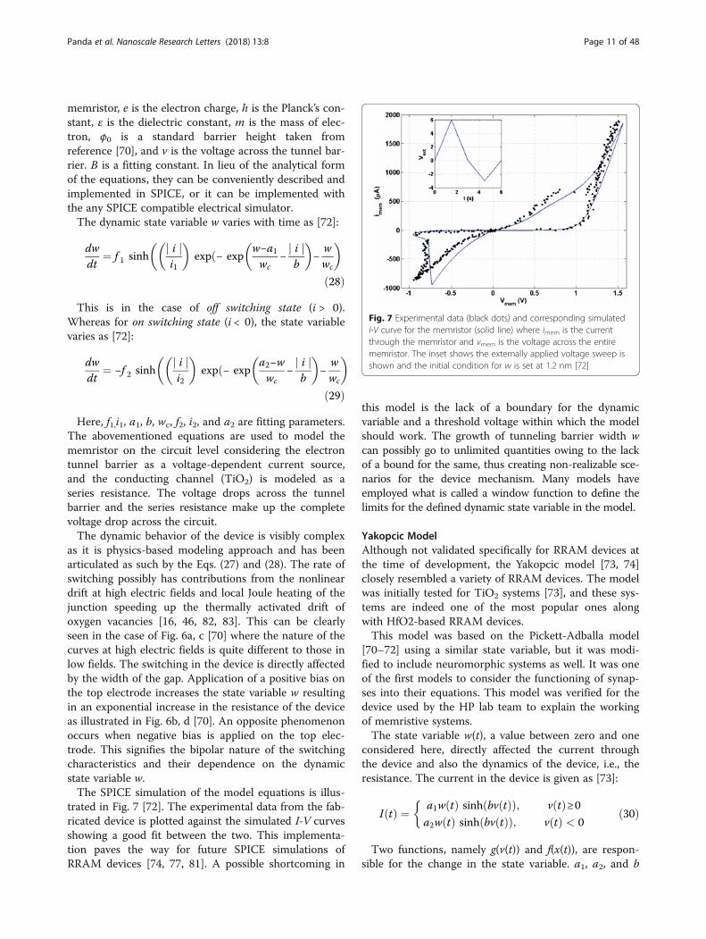
trated in Fig. 7 [72]. The experimental data from the fab-ricated device is plotted against the simulated I-V curvesshowing a good fit between the two. This implementa-tion paves the way for future SPICE simulations ofRRAM devices [74, 77, 81]. A possible shortcoming in
this model is the lack of a boundary for the dynamicvariable and a threshold voltage within which the modelshould work. The growth of tunneling barrier width wcan possibly go to unlimited quantities owing to the lackof a bound for the same, thus creating non-realizable sce-narios for the device mechanism. Many models haveemployed what is called a window function to define thelimits for the defined dynamic state variable in the model.
Yakopcic ModelAlthough not validated specifically for RRAM devices atthe time of development, the Yakopcic model [73, 74]closely resembled a variety of RRAM devices. The modelwas initially tested for TiO2 systems [73], and these sys-tems are indeed one of the most popular ones alongwith HfO2-based RRAM devices.This model was based on the Pickett-Adballa model
[70–72] using a similar state variable, but it was modi-fied to include neuromorphic systems as well. It was oneof the first models to consider the functioning of synap-ses into their equations. This model was verified for thedevice used by the HP lab team to explain the workingof memristive systems.The state variable w(t), a value between zero and one
considered here, directly affected the current throughthe device and also the dynamics of the device, i.e., theresistance. The current in the device is given as [73]:
I tð Þ ¼ a1w tð Þ sinh bv tð Þð Þ; v tð Þ≥0a2w tð Þ sinh bv tð Þð Þ; v tð Þ < 0
�ð30Þ
Two functions, namely g(v(t)) and f(x(t)), are respon-sible for the change in the state variable. a1, a2, and b
Fig. 7 Experimental data (black dots) and corresponding simulatedI-V curve for the memristor (solid line) where imem is the currentthrough the memristor and vmem is the voltage across the entirememristor. The inset shows the externally applied voltage sweep isshown and the initial condition for w is set at 1.2 nm [72]
Panda et al. Nanoscale Research Letters (2018) 13:8 Page 11 of 48
are fitting constants. Change of the state of the variableis generally governed by a threshold voltage, i.e., there isa physical change in the device structure above a certainthreshold voltage. The function g(v(t)) here models theON and OFF voltages of the device which also takes intoaccount the polarity of the input voltage. This results ina better fit to the experimental data in case of bipolarswitching where the values of set (vp) and reset (vn) volt-age, i.e., the thresholds are different. It is defined as [73]:
g v tð Þð Þ ¼Ap ev tð Þ−evp�
; v tð Þ > vp
−An e−v tð Þ−evn�
; v tð Þ < −vn
0; −vn≤v tð Þ≤vp
8>><>>:
ð31Þ
Ap and An indicate the rate of the change of state oncethe voltage threshold is crossed. It can be understood asthe dissolution or the rupture of the filament in terms ofRRAM devices. There is in-built support for thresholdvalues in the model, which enhances its applicability.The state change variable modeled by the function
f(w(t)) is used to define the boundaries for the variable.It explains the motion of the charge carrying particlesbased on the threshold values, also adding the possibilityto define the motion of the particles based on the polarityof the input voltage. This basically acts as a window func-tion which restricts the state change variable within cer-tain boundary given as [73]:
f wð Þ ¼ e−αp w−wpð Þf p w;wp�
; w≥wp
1; w < wp
(
ð32Þ
f wð Þ ¼ eαn wþwn−1ð Þf n w;wnð Þ; w≤1−wn
1; w > 1−wn
(
ð33Þ
Here, fp(w,wp) is a window function which limits thevalue of f(w) to 0 when x(t) = 1 and v(t) > 0. fn(w,wn) is asimilar window function which does not allow the valueof w(t) to become less than zero when the current flowis reversed.The window functions are defined as [73]:
f p w;wp� ¼ wp−w
1−wpþ 1 ð34Þ
f n w;wnð Þ ¼ w1−wn
ð35Þ
The movement of dynamic state variable, in simplewords, the rate of switching, is governed by a differentialequation. The growth and decay of the tunneling barrier
width are the defining mechanism for this particularmodel, and it is given by [73]:
dwdt
¼ g v tð Þð Þf w tð Þð Þ ð36Þ
Owing to the analytical nature of the coupled equa-tions, they can be solved using a mathematical solversuch as MATLAB [138, 139]. The differential equa-tion can also be solved in MATLAB using the in-built solvers idt() and ddt() functions, which employthe time step integration method. This particularmodel was simulated using the characterization dataof the TiO2 memristor from HP Labs [3], and the fit-ting obtained was pretty good when the fitting pa-rameters are properly calibrated.A separate SPICE implementation of the same
model was reported by Yakopcic et al. [74] whichwere fitted and characterized for a multitude of de-vices for both sinusoidal and repeated sweep inputs.The SPICE implementation revealed a good accuracyand applicability of the model at the circuit level. Themodel was correlated with a variety of experimentaldata, and low error rates of about 6% were obtained.It was one of the first SPICE implementation wherethe model was tested under sinusoidal as well as re-petitive sweeping inputs. This helps in determiningthe AC behavior of the device. Along with that, veryimportant device variability analysis is performedwhich defines the error tolerance in the device. Vari-ability is an important issue, when the RRAM deviceis used in large systems, such as arrays. The variabil-ity analysis performed is essential in knowing untilwhich point the system can tolerate the variability.After reaching the critical point, there is possibility oferrors in device read/write.The model was also tested for read/write operations
using 256 devices, which helps determine its usabilityin crossbar arrays. Similarly, it can be used for neuro-morphic read/write operations to test the model applic-ability in that system. Device variability in the model isdefined with change in the device parameters. So, chan-ging the device parameters leads to a change in thesimulated device I-V which is very useful in fitting themodel with the experimental data. The values of the de-vice parameters used can help define the acceptedvalues of the particular parameters in the real case sce-nario. No convergence errors were found in the 256array system, but with new RRAM array systems reach-ing higher density, applicability of the model there re-mains a question. Higher density array systemsgenerally pose a convergence problem in SPICE simula-tions, but with proper parameter definition, it can beavoided. This model can be considered a new paradigm
Panda et al. Nanoscale Research Letters (2018) 13:8 Page 12 of 48
when it comes to circuit level SPICE simulations, vari-ability analysis, and read/write operation simulationsfor RRAM devices.
TEAM/VTEAM ModelThreshold Adaptive Memristor (TEAM) model [75, 76]builds based on the Simmons Tunneling Barrier model[70–72] (discussed in the “Simmons Tunneling BarrierModel” section) and delivers a much simpler physics-based modeling approach for memristive systems. I-Vrelationship in this case is not fixed and can be chosento fit any device which provides some amount of flexibil-ity in the model. TEAM model arose from the need ofsimpler analytical equations which describe the mechan-ism of memristive systems accurately and which takeless computation time.This model is based on the approximation of the
high non-linear dependence of the memristive devicecurrent; the device can be modeled as a device withthreshold currents. The results are evident in Fig. 8.As with the tunneling barrier model, the internalstate derivate is dependent on the current and thestate variable itself, which is the effective tunnelwidth. It can be modeled effectively by [76]:
dw tð Þdt
¼
koff � i tð Þioff
−1
0@
1A
αoff
� f off wð Þ; 0 < ioff < i
0; ion < i < ioff
kon � i tð Þion
−1
0@
1A
αon
� f on wð Þ; i < ion < 0
8>>>>>>>><>>>>>>>>:
ð37Þ
Variation of the state variable with time is asymmet-rical in nature, as shown in Fig. 8b. This means that theON and OFF switching times are not equal. In the Eq.(36), ion and ioff act as the current thresholds. Functionsfon and foff are window functions which bound the in-ternal state variable x(t) within [won, woff]. Window func-tions are described as [76]:
f off wð Þ ¼ exp − expw−aoffwc
� �� �; ð38Þ
f on wð Þ ¼ exp − exp −w−aonwc
� �� �; ð39Þ
The window functions describe the dependence of thederivative in the state variable x. They work well withinthe described boundaries, but the problem arises whenthe device goes beyond the boundaries. There are nolimiting parameters here, and the window function onlydescribes the state variable inside a particular limit. Ifthe device goes beyond the boundaries, it can cause con-vergence issues with the simulator and it does not makesense for good modeling practice in case of analogdevices.I-V relationship in this model is derived from the tun-
neling barrier model, as discussed in the “Simmons Tun-neling Barrier Model” section. Due to the non-linearnature of the tunneling current, the change in resistancevaries exponentially with the state variable. So, it is as-sumed that any change in the tunnel barrier widthchanges the memristance in an exponential mannerwhich deduces to [76]:
v tð Þ ¼ RONeλ=woff−wonð Þ w−wonð Þ � i tð Þ ð40Þ
Here, λ is a fitting parameter and RON the equivalenteffective resistance at the bounds.I-V relationship for this model can be seen in Fig. 8a
[76]. Although there is a presence of a pinched hyster-esis, the form and structure of the curve are not well-defined. The model is driven with a sinusoidal input of1 V. The verification done for this model is differentfrom the tunneling model [70–72] in terms of the plat-form used to simulate it. The latter model uses a SPICEmacro model [72] to describe the equations, but SPICEtakes up a significant amount of computation time.
Fig. 8 A sinusoidal input of 1 V applied to the TEAM model usingthe same fitting parameters as used in Fig. 10 [76]. The values ofRONand ROFF are set as 50 Ω and 1 kΩ, and an ideal rectangularwindow function is applied in Eqs. (38) and (37). a I-V curve and bstate variable. It is to be noted that the device is asymmetric, i.e.,switching OFF is slower than switching ON [76]
Panda et al. Nanoscale Research Letters (2018) 13:8 Page 13 of 48
Modeling in Verilog-A [140–143] is much more effi-cient, and the TEAM model [75] utilizes this functional-ity to model the equations presented by them.A slightly modified version of the TEAM model with
the introduction of voltage threshold levels was reportedby the same group, called Voltage Threshold AdaptiveMemristor model (VTEAM) [77]. Discussed TEAMmodel was based on threshold currents, whereasVTEAM is based on threshold voltages. The major ad-vantages cited for using threshold voltages is that com-parison with current causes performance and reliabilityissues if the condition is not satisfied, i.e., a low-currentthreshold will automatically have a low-voltage thresholdas well. This might affect the overall performance of thedevice. Also with a threshold voltage, there is no riskwith going overboard with high power and voltagedestroying the device as the values are automaticallycontrolled.The VTEAM follows a similar concept to the TEAM
model, being based on an expression of the derivative ofan internal state variable. The current is dependent onthe state variable itself. The only difference is inclusionof a threshold voltage. The internal state variable (w) isdefined as [77]:
dwdt
¼
koff � v tð Þvoff
−1
0@
1A
αoff
� f off wð Þ; 0 < voff < v
0; von < v < voff
kon � v tð Þvon
−1
0@
1A
αon
� f on wð Þ; v < von < 0
8>>>>>>>><>>>>>>>>:
ð41ÞSimilar to the TEAM model, the functions fon and foff
act as window functions which bound the internal statevariable w within [won, woff]. As has been assumed inthe model, current varies exponentially with the in-ternal state variable on most occasions which is definedby [77]:
i tð Þ ¼ e−λ
woff −won� w−wonð Þ
RON� v tð Þ ð42Þ
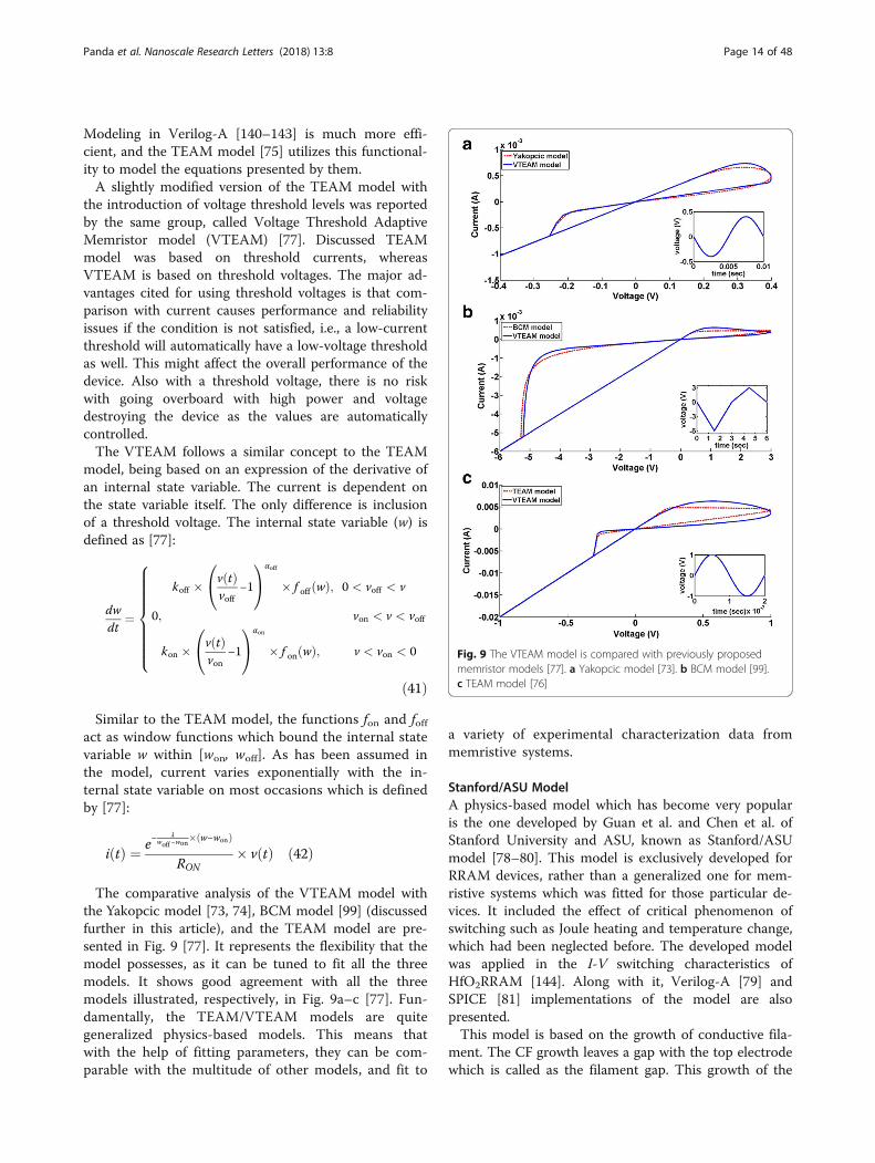
The comparative analysis of the VTEAM model withthe Yakopcic model [73, 74], BCM model [99] (discussedfurther in this article), and the TEAM model are pre-sented in Fig. 9 [77]. It represents the flexibility that themodel possesses, as it can be tuned to fit all the threemodels. It shows good agreement with all the threemodels illustrated, respectively, in Fig. 9a–c [77]. Fun-damentally, the TEAM/VTEAM models are quitegeneralized physics-based models. This means thatwith the help of fitting parameters, they can be com-parable with the multitude of other models, and fit to
a variety of experimental characterization data frommemristive systems.
Stanford/ASU ModelA physics-based model which has become very popularis the one developed by Guan et al. and Chen et al. ofStanford University and ASU, known as Stanford/ASUmodel [78–80]. This model is exclusively developed forRRAM devices, rather than a generalized one for mem-ristive systems which was fitted for those particular de-vices. It included the effect of critical phenomenon ofswitching such as Joule heating and temperature change,which had been neglected before. The developed modelwas applied in the I-V switching characteristics ofHfO2RRAM [144]. Along with it, Verilog-A [79] andSPICE [81] implementations of the model are alsopresented.This model is based on the growth of conductive fila-
ment. The CF growth leaves a gap with the top electrodewhich is called as the filament gap. This growth of the
Fig. 9 The VTEAM model is compared with previously proposedmemristor models [77]. a Yakopcic model [73]. b BCM model [99].c TEAM model [76]
Panda et al. Nanoscale Research Letters (2018) 13:8 Page 14 of 48
filament gap is considered as internal state variable inthis case. So, the rate of filament growth and the fila-ment gap govern the dynamics of the model. The fila-ment growth is explained due to the movement ofoxygen ions and vacancy regeneration and recombin-ation [145]. Considering the gap value g (nominally inthe range of 0–3 nm) to be the state variable, the rate ofchange of g is defined as [78]:
dgdt
¼ ν0 exp−Ea;m
kbT
� �sinh
qahγvLkbT
� �ð43Þ
The parameter Ea is the activation energy for vacancygeneration and oxygen vacancy migration in the SETand RESET processes, respectively. v is the applied volt-age across the device, ν0 the velocity containing theattempt-to-escape frequency, L the switching materialthickness and ah, the hopping site distance.A significant feature of this model is the inclusion of
variations in the model caused due to the stochasticproperty of the ion process and the spatial variation inthe gap size among multiple filaments. To account forthese variations in the model, a noise signal is added tothe gap distance as [78]:
g j t þ Δt ¼ F gjt; dgdt
� �þ δg � X
�nð ÞΔt; n ¼ t
TGN
ð44ÞThe variation in the gap size δg is defined as a function
of the ions’ kinetic energy and invariably on thetemperature in the filament and is given as [78]:
δg Tð Þ ¼ δ0g
1þ exp T crit−Tð ÞT amb
h in o ð45Þ
Here, Tcrit is defined as a threshold temperature be-yond which there is a significant change in the gap size.This can be understood as the point where the deviceundergoes a physical transformation such as transition-ing into a SET or RESET state. In this case, threshold isconsidered in terms of temperature, rather than voltageor current, whatever employed in the previous models[75–77]. So, the equation basically depicts the resistancefluctuation that occurs when the CF temperature is in-creased beyond the room temperature.Now that temperature can be considered a critical
driving force in the model, a modified form of thesteady-state Fourier heat flow equation is implementedin this model. Rather than considering heat flowthroughout the filament, the vicinity of the tip of thefilament is considered. There is a dynamic inner domaintemperature T which significantly changes with changein the cell characteristics, and an outer domain remainsat an ambient room temperature Tamb, related as [78]:
cp∂T∂t
¼ v tð Þi tð Þ−k T−T ambð Þ ð46Þ
cp is the effective heat capacitance of the inner domain,and k the effective thermal conductivity are both fittedbased on the type of oxide and electrodes used in theRRAM system. RESET transition from LRS to HRS gen-erally has higher temperature associated with it acrossthe device, while the SET transition has a considerablylower temperature. The current inside the device ismodeled using a generalized conduction mechanismwhere the tunneling distance and field strength have anexponential relationship. This is true in case of tunnelingcurrent conduction mechanisms such as Poole-Frenkel,Fowler-Nordhiem, trap-assisted, or direct tunneling [9,16, 46, 49, 51, 55]; these are the mechanisms most com-monly associated with RRAM systems [51, 55, 61, 66].The current conduction is defined as [78].
i g; vð Þ ¼ i0 exp−gg0
� �sinh
vv0
� �ð47Þ
The advantage with a generalized current equation isthat for a particular device if some other mechanism isfitting better, it can be incorporated easily by adding therequired parameters and adjusting their values accord-ingly. I-V response of the model compared with experi-mental data is shown in Fig. 10. The experimentalresponse is shown in Fig. 10a while the simulated curveis shown in Fig. 10b. Simulated transient response showsthe capabilities of the model in taking variations into ac-count. Developed model was verified using Ngspice[146] as a macrocircuit. Ngspice is an open sourceSPICE simulator which is quite efficient and convenientfor doing DC and AC analysis. This model can be imple-mented in MLC memory circuits and also to verify theefficiency of programming strategies and error correc-tion codes [78].A major feature of this model is implemented in the
neuromorphic systems and RRAM synaptic device de-sign [147]. This model has been tested against a HfOx/TiOx multi-stack RRAM system [148] which is imple-mented in a neuromorphic system. This gives the modelgreat flexibility and wide applications as there are only afew models that are actually applicable for neuromorphicsystems. Also, the model defined for these systems hasbeen deemed tolerant to training error caused by devicevariation [149]. The gradual resistance modulationwhich is critical to the learning process in a synaptic de-vice can be quantified in the model [150] which marks asignificant development in using RRAM synaptic stacksin neuromorphic computing systems.
Panda et al. Nanoscale Research Letters (2018) 13:8 Page 15 of 48
Physical Electro-Thermal ModelThis model is an extensive physical model which de-scribes the bipolar operation in RRAM devices usingequations closely resembling the physical mechanisms.This model was reported by Kim et al. [87], and it wasverified with a tantalum pentoxide (Ta2O5)-based bi-layered RRAM structure [15, 151, 152]. It makes use ofthe finite element solving method employed in the pre-vious model to solve the differential equations. Themajor value addition by this model over the model pro-posed by Larentis et al. [86] was the proper descriptionprovided for the SET state in the bipolar RRAM device.The previous model was inadequate in accommodatingthe complete transition and explaining it properly butthis model makes up for that. Also, it improved upon aphysical electro-thermal model reported by Menzel et al.[153] which attempts at calculating the CF temperatureprecisely.It also uses the electro-thermal physics phenomenon
approach for modeling which we have seen in the previ-ous model [86]. The major advantage with models basedon this concept is their ease of use owing to the simplefundamental equations and the flexibility to employ aproper finite element method (FEM) solver to simulatethe system very accurately. But a major disadvantage isthat the model becomes very difficult to implement incircuit solvers based on SPICE and providing an equiva-lent implementation in Verilog. This is because of thelack of support in SPICE and Verilog for properly defin-ing partial differential equations which make up for thevastness of the model. Normal ordinary differentialequations and the ones which are in analytical form canbe solved in circuit solvers but partial differential equa-tions (PDE) cannot be solved.
Electro-thermal models are equally important ascompared to the other physics-based models discussedbefore because temperature is an important factorgoverning the set and reset processes. Ion and vacancymigration plays a dominant role for switching mechan-ism [16, 46], although the governing factors are behindthis process and the exact type of ions is still up for de-bate. So, the fact that temperature is a governing factorin this process makes these models attention worthy.Also, experiments [85, 154] in this regard suggest thatthere is significant change in the temperature in the CFduring the switching process. Some of the previousmodels discussed above have neglected this effect byconsidering conducting filament-oxide interface to beat room temperature or by taking constant conductingfilament temperature [39, 86, 88, 89, 144].The major difference between this model and the pre-
viously discussed electro-thermal model is in the expres-sions used to describe the drift-diffusion process. CF isdescribed as a doped region where the oxygen vacan-cies act as dopants, and the CF runs from the top elec-trode to the bottom electrode. This is an assumptionthat many models take that the CF runs from one endof the electrode to the other when the state variable isconsidered as the length of CF. A few models discussedpreviously [78, 80] have used the filament gap to thetop electrode as state variable. So, the assumptions gen-erally vary from system to system and are dependent onwhat mechanism is employed to describe the device.Another assumption taken to describe the drift-
diffusion of vacancy migration is that the same equationused can describe both the oxygen ions and vacancies.This is generally the case to simplify the model and re-duce the complexity of the equations. The rigid point
Fig. 10 a Experimental and b simulated transient responses of a HfOx RRAM device to the − 2.3 V 50 ns input pulses. The experimental result isreported elsewhere [144] and included here in a for convenience. c In a larger time range, the simulated transient response for the same deviceincluding the gap size and temperature is shown. Current compliance set at 200 μA in simulation [78]
Panda et al. Nanoscale Research Letters (2018) 13:8 Page 16 of 48
ion model by Mott and Gurney [155] is employed hereto describe the process given as [87].
∂nD∂t
¼ ∇� Ds∇nD−μvnDð Þ þ G ð48Þ
where Ds describes the diffusion process, v gives the driftvelocity of the vacancies, and G is the generation rate ofvacancy or the CF growth rate which actually describesthe SET process. The G term is a specialized parameteradded to better describe the complete switching process[156, 157]. The parameters are defined as [87]:
Ds ¼ 12� a2 � f e � exp −Ea=kBTð Þ ð49Þ
v ¼ ah � f � exp −Ea=kBTð Þ � sinh qahE=kBTð Þð50Þ
G ¼ A� exp − Ea−qlmEð Þ=kBTð Þ ð51ÞHere, lm is the mesh size. So, using the Eqs. (48)–(50),
the oxygen vacancy transport given in Eq. (47) can bedefined which contains all the factors of drift-diffusionas well as the vacancy regeneration. These equationsgovern the CF growth and rupture which defines thephysical transformation of the device during the SETand RESET transition of the device. So, it basically acts
as a dynamic internal state variable which controls theswitching rate of the device.The simulation results for the reset transition is shown
in Fig. 11 [87]. Concentration of the oxygen ions isshown at different voltages in Fig. 11a [87] which invari-ably governs the switching in the device. The point C(3.0 V) is the point where the reset transition occurs, sothe concentration of ions is also the highest at the in-terfaces for that voltage point as evident in Fig. 11b[87]. On similar lines, the temperature and flux areon the higher side which can be seen in Fig. 11c, d,respectively [87].Equations (95) and (98)mentioned further are also
used in the model to describe the current conductionand the temperature change due to Joule heating in thedevice. The equations are simultaneously solved inCOMSOL to generate the required simulated profiles.The obtained simulated profiles are compared and veri-fied against a TaOx bi-layered RRAM system [87]. Inaddition to the DC I-V characteristics the model wasalso used to generate time-dependent reset characteris-tics by investigating its response to square pulses.
Huang’s Physical ModelA very comprehensive physical model of RRAM devicesis developed by Huang et al. [88, 89]. Its major feature is
Fig. 11 Simulation results for the reset transition of the device. a Vo density (nD) map. Calculated profiles of b nD, c T, and d y for states A (1.0 V),B (1.7 V), and C (3.0 V). The position of z = 15 nm indicates the Ta2O5/TaOx interface in the structure schematic. The shaded area shows thedepleted gap, defined for nD < 5 × 1021 cm-3 [87]
Panda et al. Nanoscale Research Letters (2018) 13:8 Page 17 of 48
its consideration of the multitude of factors affecting theCF dynamics in the RRAM device. This model is com-prehensive in the sense that it considers both the widthof CF as well as filament gap to the electrode as factorsaffecting the state variable dynamics. The model wasvalidated in a TiO2 based device and also applied in a2 × 2 RRAM array cell [88].Covering bipolar devices primarily, it also accounts
for the temperature distribution in the device with mul-tiple heating sources. SET/RESET process is consideredto be caused due to generation/recombination processof the oxygen ions (O2−) and oxygen vacancies (Vo).Top electrode (TE) is the active electrode and acts asan oxygen reservoir for the release or absorption ofoxygen ions [88]. The CF evolution during the SETprocess is modeled based on the width of the CF.Growth of the CF is thought to start from the tip of theactive electrode. With an increase of voltage the CF en-larges along the radius resulting in a final width of theCF as w. So, the value of w is critical to determine theLRS resistance in the SET process. Huang et al. [88] as-sumed that the CF grows in a symmetrical cylindricalshape which is simplifying at best. While the cylinderhas been the most popular to describe the shape of theCF, it might not be the most accurate.Rupture of the CF during the reset process is consid-
ered to start from the TE first. CF disconnects from thestarting point and then dissolves internally with in-crease in the voltage. Distance between the tip of theCF and the active electrode layer is defined as the fila-ment gap distance (x). The value of x determines theresistance of HRS during the RESET process. x and dx/dt are thus critical in defining the RESET process. Avery important feature of the model is that there aretwo parameters defining the state of the system, inplace of one parameter. The parameter w acts as thestate variable for the SET process and x for the RESETprocess. So dx/dt and dw/dt define the dynamics of thedevice during the SET/RESET transition. Analyticalmodel for a RRAM cell presented by Huang et al. [88]is developed by modeling the parameters x, w and theirevolving speeds.This model also presents one of the most detailed de-
scriptions for the processes involved behind the RESETprocess. The rate of the CF shortening is affected bythree processes, (a) O2− release by the electrode, (b)O2− hopping in the oxide layer, and (c) recombinationbetween O2− and Vo. Slowest process among thethree dominates the CF reduction process which isdefined by the parameter x. Speed of the processes isaffected by the specific device characteristics and theoxide used.CF reduction rate during first reset process, i.e., O2−
release by the electrode can be given as [89]:
dxdt
¼ a� f � exp −Ei−γZeV
kBT
� �ð52Þ
In case of the O2− hopping in the oxide layer, the CFwith a being the distance between two Vo, reduction rateis described by [89]:
dxdt
¼ a� f � exp −Eh
kBT
� �sinh
ahZeEkBT
� �ð53Þ
The RESET process when dominated by the recombin-ation between O2− and Vo is written as [89]:
dxdt
¼ a� f � exp −ΔEr
kBT
� �ð54Þ
The value of x is fixed to x0 after the RESET process.This invariably will act as the boundary condition forthe model. But the problem here is the value and therole of x0 is not clearly defined here. This will possiblycreate ambiguities while defining the states of the deviceor switching between two states. In the first step of theSET process which is dominated by recombination ofoxygen vacancies and where a thin CF is initially grownis described by [89]:
dxdt
¼ −a� f e � exp −Ea−αaZeE
kBT
� �ð55Þ
Here, Z and αa are fitting parameters. In the secondstep, the CF grows along the radial direction of the CF isdefined as [89]:
dwdt
¼ Δwþ Δw2
2w
� �� f e � exp −
Ea−γZevkBT
� �ð56Þ
Current flowing through the device has been taken inthe model due to the hopping conduction and metallicconduction. The current in CF region can be calculatedusing the basic structures of Ohm’s law and Arrheniuslaw [158]. But the current in the gap region as a resultof hopping conduction is given a little different. It ismodeled as a correlation of the hopping current withthe voltage and gap distance is given by [147]:
i ¼ i0 exp −x=xTð Þ sinh v=vTð Þ ð57ÞTemperature effects in the model are considered from
the Filament Dissolution model [82, 83] discussed fur-ther in the “Filament Dissolution Model” section. Valid-ation of the model is performed in HfOx/TiOx system[88, 89]. Transient results obtained from simulating themodel are compared against the data from the device,which shows a good match as demonstrated by Huanget al. [88]. The model is also validated against devicesfabricated by other groups [144, 159] and the parametersare adjusted accordingly. A pretty accurate match
Panda et al. Nanoscale Research Letters (2018) 13:8 Page 18 of 48
between the simulation and the experimental resultssuggests a good level of flexibility with the model. Themodel also demonstrates that the switching speed of thedevice is highly dependent on the input voltage sweeprate.Although the model is very comprehensive and takes
into account a variety of detailed processes affecting theRRAM operation; it has some critical shortcomings. Amajor one is the non-compatibility with SPICE orVerilog-A. Implementations in any of the circuit simula-tors based on these platforms has not been demon-strated which raises a question on its readiness forsimulations. Also, boundary conditions and non-lineareffects have not been applied in the model which leavesit open to unphysical solutions. There has been no at-tempt to fit a window function with the model to ac-count for this effect. These shortcomings make themodel difficult for application for simulations, but itsphysics give a lot of insights into the functioning ofRRAM devices.
Bocquet Bipolar ModelA very interesting and unique model from Bocquet et al.[90, 92] which utilizes a physics based modeling ap-proach to describe bipolar oxide based resistive switch-ing memories. This was a model developed exclusivelyfor the RRAM devices. Although a point of speculationstill exists, it has been more or less accepted that the bi-polar resistive switching mechanism is governed by thevalence change mechanism which occurs in specifictransition metal oxides and the field-assisted motion ofoxygen ions O2− [160].This is also one of the few models that can describe
electroforming process. This process basically initiatesthe CF growth for the first time when the device is in apristine state. It requires significantly higher voltage ascompared to the set or reset voltage because the CF for-mation requires an electric breakdown of the oxide andthis requires higher voltage and energy. However, form-ing free RRAM devices have been reported [85] byadjusting the oxygen stoichiometry of the active layer.Removal of the forming process will reduce the voltagerequirement of the device and make it more energyefficient.Bocquet bipolar model uses some concepts from the
Bocquet unipolar model [90] and modifies it significantlyaccording to the bipolar switching characteristics. Majorfeatures of the model are its intrinsic simplicity in themodel equations, full compatibility with SPICE basedelectric simulators and inclusion of voltage and time de-pendencies of the device. Internal state variable here isthe radius of the CF which governs the switching rate.Radius of the CF varies with growth/rupture mechanismof the CF which is explained in the model with the help
of local electrochemical redox processes [82, 83, 105, 161]which are dependent on the applied bias polarity. A singlemaster equation in which both the SET and RESET pro-cesses are accounted for simultaneously is controlled bythe CF radius which thus gives the switching rate of thedevice.Electroforming stage is modeled using electroforming
rate which describes the process of conversion of thepristine oxide into a switchable sub-oxide layer. CF ra-dius (rCF) varies from a minimum value of 0 to a max-imum value of rCFmax. The electroforming stage ismodeled as [92]:
τform ¼ τform0 � eEaForm−q � αs � vCell
kb � Tð58Þ
drCFmax
dx¼ rwork−rCFmax
τformð59Þ
Some of the simplifying assumptions in the model areregarding the current conduction in the LRS and HRS.During the LRS, the conduction is assumed to beOhmic, i.e., it follows Ohm’s law. In the HRS region, thecurrent is dominated by a leakage current in the sub-oxide region which is basically due to trap-assisted con-duction, but for simplicity sake, Ohmic conduction isconsidered here. The SET/RESET operation in themodel is described by the electrochemical redox reactionderived from the Butler-Volmer equation [162] givenas [92]:
τRed ¼ τRedox � eEa−q�αs�V cell
kb�T ð60Þ
τOx ¼ τRedox � eEaþq� 1−αsð Þ�VCell
kb�T ð61Þ
Here, τRed and τOx are the reduction and oxidation re-action rates, respectively. τRedox is the effective reactionrate considering both the reduction and oxidation reac-tions. Above two equations are coupled together in amaster equation which define the switching rate givenas [92]:
drCFdt
¼ rCFmax−rCFτred
−rCFτOx
ð62Þ
This is quite a comprehensive model in the sense thatit includes the temperature effects as well. Temperatureplays a significant role in the redox reaction rates[163, 164] and thus the local temperature in the fila-ment is a very important parameter in this regard.The basic heat equation is used in this model andmodified it accordingly given as [92]:
Panda et al. Nanoscale Research Letters (2018) 13:8 Page 19 of 48
σ xð Þ � E xð Þ2 ¼ −k � ∂2T xð Þ∂x2
ð63Þ
T xð Þ ¼ T amb þ vCell2
2� L2x � k� L2x
4−x2
� �� σeq ð64Þ
T ¼ T amb þ vCell2
8� k� σeq ð65Þ
σeq ¼ σCF � r2CFrwork2 −σOx �
rCFmax2− r2CF
r2workð66Þ
On the face of it, the equations seem pretty complexto evaluate. But in reality, they are analytical in naturewhich makes them easily solvable in a numeric solverand can be implemented in an electric simulator. This isa major advantage of this model. Almost all of themodels which employ the concept of temperaturechange in the filament follow the basic principles of thefilament dissolution model [82, 83] discussed further inthe “Filament Dissolution Model” section. During set op-eration, the temperature rises due to the increase in theCF radius, while it falls due to a decrease in the CF ra-dius during the reset operation. This creates a positivefeedback loop between the two processes leading to aself-accelerated reaction. This forms the basis of the fila-ment dissolution model and all models incorporatingthe temperature effects in the device converge on thisphenomenon [82, 83, 86–89, 92].I-V characteristics of NiO based RRAM along with
simulated curve using Bocquet model is presented inFig. 12 [91]. Figure 12a represents the set and reset tran-sitions of the device while Fig. 12b highlights the form-ing process. The current conduction in the Bocquet
bipolar model is treated a little differently from what wehave seen from previous models [87, 88, 90]. It considersthe current as a combination of contributions from threedifferent sources. The first one is the current from theconductive area (iCF), the second is the conductionthrough the switchable sub-oxide (isub-oxide) and then theconduction through the pristine device (ipristine). Thetotal current is described as [92]:
icell ¼ isub−oxide þ iCF þ ipristine ð67Þ
iCF ¼ E � π � σCF � r2CF ð68Þ
isub−oxide ¼ E � π � σox � r2CFmax−r2CF
� ð69Þ
ipristine ¼ Scell � Ae � E2 � exp−Be
Eð70Þ
Ae ¼ me � q3
8π � h�moxe � ϕb
ð71Þ
The parameter Be is metal-oxide barrier height (ϕb),dependent which is given as [92]:
if ϕb≥qLxE : Be ¼8π
ffiffiffiffiffiffiffiffiffiffi2mox
e
p3� h� q
ϕ32b− ϕb−qLxEð Þ32
h i
otherwise : Be ¼8π
ffiffiffiffiffiffiffiffiffiffi2mox
e
p3� h� q
� ϕ3=2b ð72Þ
Here, Scell is a section of the RRAM cell. Ae and Be areadditional parameters defined to make the equationsconcise. To implement the model in an electrical simula-tor, discrete solutions are required which are well
Fig. 12 a, b Experimental I (V) characteristics for Electroforming, Set, and Reset processes measured on a large number of memory elements tounderstand the device-to-device variability. The experimental device-to-device variability is accounted for in Monte Carlo simulations with a ± 5%standard deviation on parameters α and Lx [21]
Panda et al. Nanoscale Research Letters (2018) 13:8 Page 20 of 48
provided in this model. This makes the model suitablefor proper simulation involving electrical circuits, thuswidening its use case scenario. In this model, theequations are implemented in an Eldo circuit simula-tor [165, 166]. Memory effect of the device was repli-cated in the form that for each cell of the RRAMinstance during transient simulation, the previousstate of the filament as well as the applied voltage aregiven as the present state of the device [92]. Newstate gets solved as a function of these new inputsand the time step considers in the transient simula-tion. The discrete solutions are given as [92]:
rCFmaxiþ1 ¼ rCFmaxi−rworkð Þ � e−Δt
τForm þ rwork ð73Þ
rCFiþ1 ¼ rCFi−rCFmaxi �τeqτRed
� �� e
−Δtτeq þ rCFmaxi �
τeqτRed
ð74Þ
where τeq ¼ τRed � τOx
τRed þ τOxð75Þ
The model has been verified against electricalcharacterization from an HfO2 based system [167]. Tobetter judge the model on circuit level, a 2T/1R bipolarOxRAM [168] cell was simulated using Eldo, as shownin Fig. 13a [92]. Simulation of this type helps check thestability of the model when applied to a system environ-ment. Current variation, voltage, and CF radius (rCF) areshown with respect to time. Voltage follows a triangularwave form, which is the input sweep. Current in the de-vice transitions from high to low and vice-versa dependon the voltage levels. The sudden drop in the currentlevels, as shown in Fig. 13b [92], indicates the devicetransition. CF radius follows a similar path as thecurrent which is expected behavior of the internal statevariable.
Another important feature of OxRAM that has beenhighlighted in the model is the soft-reset [168]. It mainlyinduces the dependence between resistance in HRS andthe stop voltage during the preceding reset operation.This phenomenon is basically due to the incomplete de-struction of the CF during the reset process. So, the CFradius and temperature decrease during this process,leading to a decrease in the reaction rate. This meansa self-limited reaction rate thus getting the name soft-Reset. This model can account for the device to devicevariability very efficiently [169, 170]. The standard de-viation obtained for the important parameters such asthe length of the oxide (Lx) is well within the acceptedrange, thus accounting for the variations when thematerials change in different devices [167, 168].A shortcoming in the model which can be highlighted
is the lack of a voltage or current threshold. Also, itworks on the simplifying assumption that the CF radiusgrows from one end of the top electrode to the otherend of the bottom electrode. This makes the model im-mune to significant fluctuations if the growth of the CFis not complete, thus leaving a filament gap. There is noprovision to account for the effect of the filament gap ifit occurs.
Berco-Tseng ModelThe proposed model and simulation approach [171–175]by Berco-Tseng for RRAM devices is based on describingthe CF growth process. The Gibbs free energy criteria[174, 175] is used as an indicator to model the growth dy-namics of the CF. Simulation approach for the form-ing, set and reset process in the model is based onthe Metropolis Monte Carlo algorithm [174]. This ap-proach importantly does not rely on time evolution ofthe CF, thus increasing the efficiency of comparisonof the relative retention properties of MIM structures.The model is quite comprehensive in terms of describ-
ing the underlying physical parameters which affect theCF kinetics in the resistive switching layer. It also intro-duces the concept of “hot-spots” [172–174] which arerandom localized initial clustering of oxygen vacancieswhich facilitate the formation of the CF. The major par-ameter governing the Gibbs free energy is the enthalpyof formation of an oxygen vacancy [174] is used to de-fine the CF growth dynamics in the switching layer andintegrate it into the Monte Carlo simulator. As a result,all the CF processes, namely forming, set and reset canbe effectively simulated.A monoclinic HfO2 switching layer is primarily used
to implement the model. But other material stacks, suchas ZrO2, Cu-HfO2 are also studied and compared withby us. Electrical conduction in the RRAM device is mod-eled on the Arrhenius relation, given as [174]:
Fig. 13 Simulating the electrical characteristics of the considered2T-1R OxRAM structure [174]
Panda et al. Nanoscale Research Letters (2018) 13:8 Page 21 of 48
σn ¼ σ0 exp −Eac
kBTn
� �ð76Þ
Typical boundary condition, such as Vdd at top elec-trode and ground at bottom electrode is applied to thedevice. For modeling the CF accurately, it is divided intoa grid structure to discretize it, which is in line with thefinite element analysis (FEA) method. The various pa-rameters defining each grid site are its spatial coordi-nates (x, y), local potential φ, temperature T, No, Nov,trap occupancy c, electrical conductivity σ and thermalconductivity kth. The various processes associated withthe evolution of CF within the oxide layer involves gen-eration, recombination and hopping of oxygen (O), oxy-gen vacancies (OV) and electrons.As a result, these processes are defined in terms of
probabilities in the MC simulator. The probabilities aredefines according to the minimum energy criteria as dis-cussed earlier. This approach smoothens out the itera-tive steps in the simulator rather than the abrupt + 1 or− 1 levels in the discrete approach. The generation (Pg),hopping (Ph), and recombination (Pr) probabilities forthe oxygen species are given as [174]:
Pg;n ¼ 1−Cnð Þ exp −Ea−aaZeE
kBTn
� �ð77Þ
Ph;n→m ¼ Cn 1−Cmð Þ exp −Eh−ahZeE
kBTn
� �ð78Þ
Pr ¼ Cn exp −ΔEr
kBTn
� �ð79Þ
Here, E is the local electric field, Cn represents the ra-tio of Nov (density of oxygen vacancies) in the low stateto the maximal one at site n (nth grid site). Ea and Eh arethe activation energies for oxygen species generationand hopping respectively. Similarly, aa and ah are thefield lowering factor for O generation and hopping.The mechanism of the current conduction is consid-
ered to be trap-assisted tunneling [171, 173, 174]through the switching layer. The Mott variable hoppingmodel [174, 175] is taken into account here to modelthe tunneling effect. Mott DC conduction considered atany two grid points m, n are given as [174]:
σmn ¼ f ee2cm 1−cnð ÞdmnkBTn
exp −2dmn
α
� �exp −
e j ∇φmn jkBTn
� �ð80Þ
Here, dmn is the distance between m and n, α is thetypical attenuation length of the electron wave functionin the trap and c being the trap occupancy.The model is simulated and the results are compared
with many different material stacks of RRAM devicesfrom other groups as well. The Fig. 14 shows the
simulated heat map of the No (density of oxygen) con-centration during the CF rupture process. The simula-tion result corroborates with the experimental results,showing wide applicability potential for the model.
Gonzalez-Cordero et al. Bipolar ModelIt is a compact physical model proposed by Gonzalez-Cordero et al. [93] describing the working of bipolarRRAM systems. The model is unique because it con-siders the CF as a truncated cone, which is a significantdeparture from previous models considering the CFshape generally as a cylinder. Also, the model is vali-dated by implementing it in Verilog-A which gives us acloser look into the description and simulation of RRAMdevices on the circuit level using Verilog-A. The pro-posed model builds upon the concepts introduced in theprevious Bocquet bipolar model [91, 92] and modifies itaccordingly to suit the new CF shape proposed.One of the important aspects about the model is the
consideration of a truncated cone shaped CF [176–179].Majority of the models we have encountered till nowconsider the CF as a symmetrical cylinder which is moreof a simplifying assumption [91, 92]. This is because ithas been shown that the CF can grow [39, 51, 55] fromone end of either electrode to the other depending on
Fig. 14 Resistive switching layer and Ti/HfO2 interface oxygen spatialdensity (No) plot during the CF rupture using negative bias: a initialand b final [174]
Panda et al. Nanoscale Research Letters (2018) 13:8 Page 22 of 48
the active electrode. So, it is quite possible that the CFin this case might not be a perfect cylinder. So, a trun-cated cone is equipped to account for any variability andfluctuations arising due to the shape of the CF. Shapesother than simplified geometrical shapes are not consid-ered in the models because of algebraic complexities. Inprevious models [91, 92], we noticed that device to de-vice and cycle to cycle variability’s have a significant ef-fect on the application of particular models to devices.So, by taking a truncated cone as the CF shape providesthis model more flexibility than the others.Another significant feature is the role of temperature in
the CF and the reset process. Majority of the modelswhich describe the CF rupture due to the self-accelerateddissolution, consider that the process takes place at the CFnarrowing point and temperature increases at that par-ticular point [82–84, 91, 92]. This point is generally in themiddle of the cylindrical CF due to its symmetry. So, whenwe look at it from a physical standing point, thetemperature at each of the points in all the RRAMsstacked together in a circuit has to be evaluated. Realizingthis from the circuital standing point and simulating thou-sands of devices in the circuits is a very time-consumingprocess and slows down the simulation. This problem canbe circumvented by considering two temperatures in theCF instead of the general single temperature; this ap-proach also keeps the simplicity of the model intact. Twotemperatures represent the main CF body that is notdestroyed during the reset operation and the CF narrow-ing. This has been implemented in this model by consid-ering the two temperatures as the wide region and thenarrow region of the truncated cone, respectively.This model extends the previously discussed Bocquet
bipolar model [91, 92] in the “Bocquet Bipolar Model”section. In the previous model, the equations were de-fined keeping a cylindrical CF in mind, so the equationshere have been modified to account for the change inthe CF shape. The truncated cone CF is described bytwo different radii. CF is considered to grow from thetop electrode to the bottom; the interface radius withthe top electrode (TE) is rCFT which is always greaterthan the radius of the interface with the bottom elec-trode (BE) rCFB. This adheres to the structure of thetruncated cone. An assumption is made here that duringCF rupture, height of the cone is not affected; this makesthe model open to fluctuations if there is any filamentgap produced due to premature growth of CF. Althougha forming process is considered for the device, it is notincluded in the model making the model not suitable forapplication to devices where forming is a significant fac-tor. A possible explanation for leaving out the formingprocess is to avoid adding more complexity to the modelbecause the forming parameters have to be included inthe set/reset equations as well.
Similar to the previous model, the set/reset processesare described by an electrochemical redox reaction anddiffusion processes [82–84, 105, 161, 162] which controlthe growth and rupture of the CF, respectively. The re-duction and oxidation reaction rates are given as [93]:
1τRed T ;Bð Þ
¼ ARedox � e−Ea−q�αs�v T ;Bð ÞkB�TCF T ;Bð Þ ð81Þ
1τOx T ;Bð Þ
¼ ARedox � e−Ea−q� 1−αsð Þ�v T ;Bð Þ
kb�TCF T ;Bð Þ ð82Þ
Velocity of the CF radius increase/decrease which isbasically the switching rate is controlled by two masterdifferential equations which include the top (rCF,T) andbottom (rCF,B) radius of the CF. They are given as [93]:
drCFT
dt¼ rCFTM−rCFT
τRedT
−rCFT
τOxTð83Þ
drCFB
dt¼ rCFT−rCFB
τRedB
−rCFB
τOxBð84Þ
CF radius is set a boundary which defines the limitsfor the CF growth/rupture which is given as [93]:
rCFTm ≤rCFT ≤rCFTM ð85ÞrCFB ≤rCFBM ð86Þ
Here rCF,TM/rCF,BM is the maximum top/bottom radiusthat can be achieved and rCF,Tm the minimum value ofthe top radius. This equation indicates CF geometry fol-lowing a truncated cone structure and the top radius isgreater than the bottom radius at all times. The modelemploys a numeric solving method similar to the oneused in the previous model to find the discrete solutionsfor the master differential equations. But the solution forthis model is not found, which means it is difficult tovalidate the reliability of the equations.A very interesting point here is that a separate local
diffusion process is not added in this model to describethe reset process in addition to the oxidation/reductionprocess. Many of the previously discussed models [91, 92]have a separate equation for the diffusion. But in thismodel diffusion has been integrated into the Eqs. (80) and(81) for redox reactions by considering different activationenergies for the reduction and oxidation rates. This hasbeen deliberately done considering the fact that the equa-tion used in previous models to describe the diffusion vel-ocity is similar in structure to the redox equations. As aresult, the activation energies for both are combined to-gether to consider a single activation energy which in-cludes diffusion as well.The current in the RRAM device is considered to be
comprised of two components, the CF current (iCF) and
Panda et al. Nanoscale Research Letters (2018) 13:8 Page 23 of 48
the oxide current (iox). In CF current, contribution ofthe CF resistance (RCF) and the oxide surrounding theCF included in the CF radius are given as [93]:
iCF ¼ vappRCF‖Rox
ð87Þ
RCF ¼ Lπ � σCF � rCFT � rCFB
ð88Þ
Rox ¼
L� β
2� σox � π � rCFext � rCFB−rCFTð Þ; rCFT≠rCFB
L
σox � π � r2CFext−r2CFT
� � ; rCFT ¼ rCFB
8>>>>><>>>>>:
ð89Þ
The other component in the device current, i.e., theoxide current represents the current throughout theoxide accounting for the whole area of the device exceptthe one occupied the CF. The oxide current is describedas [93]:
iox ¼ sign vapp� � AHRS � SCell � j vapp j
L
� αHRS
ð90Þ
Here, AHRS and αHRS are fitting constants. The experi-mental and simulated results from the model are illus-trated in Fig. 15 [93]. The simulated I-V curves weretuned using device parameters to fit the reported experi-mental data [180]. The major device parameter whichwas tuned the CF radius. Simulated results are almost aperfect fit to the experiment results which highlights the
flexibility of the model with the proper tuning ofparameters.When considering electrochemical redox reactions,
temperature is a very important factor. As can be seenfrom the equations describing the set/reset process,temperature parameter is a defining factor. Modelingusing this concept, temperature in the CF is describedthrough a one-dimensional approach as given as [93]:
σCF � E xð Þ2 ¼ 2chrCF xð Þ TCF xð Þ−Toxð Þ−k ∂
2TCF xð Þ∂x2
ð91Þ
However, this approach is not the best one for trun-cated cones. It leads to increased complexity and im-proper calculation of temperature. So, Gonzelez-Corderoet al. [93] proposed a different approach where they havedeveloped simplified analytical equations which are suit-able for simulation. In the previous Bocquet model [92]they have assumed a cylindrical uniform geometry wherethe calculated unique temperature is uniform through-out the CF. But to consider a more detailed physical de-scription in this model; they have considered twotemperatures in the CF. One temperature is at the hot-test CF point where the reset process ruptures the CFand the other temperature is considering the main CFvolume. This is a more reasonable model for a truncatedcone structure as the two radii grow independently ofeach other depending on the oxidation/reduction pro-cesses [171, 181].To mask this concept into a simplified analytic expres-
sion, a simplifying assumption is made. Uniform cylin-ders are considered to represent the truncated cone CF;one corresponding to the larger radius of the cone, i.e.,
Fig. 15 a RRAM current versus voltage for different cycles; the CF features are tuned to fit different curves such as rCFTM = 45 nm, rCFTm = 15 nm,and rCFBM = 7 nm for cycle 3, rCFTM = 45 nm, rCFTm = 25 nm, and rCFBM = 7 nm for cycle 31, and rCFTM = 40 nm, rCFTm = 35 nm, and rCFBM = 7.8 nmfor cycle 60; b I-V curves for the devices under consideration along with different modeled data (the CFs’ dimensions considered to fit the wholeset of curves have been generated randomly). The temperature at the most representative points of the I–V curve, highlighted in a cycle 3:TSET (T,B) = [579,656] K, TLRS+ (T,B) = [349,368] K, TLRS-(T,B) = [466,525] K, TRESET (T,B) = [565,621] K; cycle 31: TSET (T,B) = [573,669] K, TLRS+ (T,B) = [349,368] K, TLRS-(T,B) = [460,525] K, TRESET (T,B) = [566,622] K; cycle 60: TSET (T,B) = [564,685] K, TLRS+ (T,B) = [347,367] K, TLRS- (T,B) = [460,525] K, TRESET (T,B) = [545,641] K [93]
Panda et al. Nanoscale Research Letters (2018) 13:8 Page 24 of 48
rCF,T and the other to the smaller radius, i.e., rCF,B. So,the maximum temperature calculated for each cylinderconsidering the main CF volume (TCF,T) and at the nar-rowest part (TCF,B) is given as [93]:
TCF T ;Bð Þ ¼ T amb þσCF T ;Bð Þ � rCF T ;Bð Þ � E2
T ;Bð Þ2� ch
1− coshα T ;Bð ÞL
2
� �� �þ dT0 T ;Bð Þ
α T ;Bð Þsinh
α T ;Bð ÞL2
� �ð92Þ
α T ;Bð Þ ¼ffiffiffiffiffiffiffiffiffiffiffiffiffiffiffiffiffiffiffiffiffi
2hk � rCF T ;Bð Þ
sð93Þ
dT0 T ;Bð Þ ¼σCF T ;Bð Þ � rCF T ;Bð Þ � ξ2T ;Bð Þ tanh
α T ;Bð ÞL2
� �ffiffiffiffiffiffiffiffiffiffiffiffiffiffiffiffiffiffiffiffiffiffiffiffiffiffiffiffiffiffiffiffiffiffiffiffiffiffiffi2� k � ch � rCF T ;Bð Þ
p ð94Þ
σCF T ;Bð Þ ¼σCF0
1þ αT TCF T ;Bð Þ−T amb
� � ð95Þ
Here, αT is the conductivity temperature coefficient.The model is simulated and compared with the resultsfrom the previous Bocquet bipolar model [93] on whichit is based. The results compare the findings from themodel considering a cylindrical CF to the one consider-ing the truncated cone CF. There is some evidence [93]presenting a better fit with the experimental data for thisparticular model as compared to the previous models
where cylindrical CFs are considered and also resultspertaining to the cases where multiple CFs are also pre-sented; this shows the model’s flexibility in accommodat-ing devices where multiple CFs is existent.Detailed simulation results presenting the variation of
current, voltage and CF radius are shown in Fig. 16 [93].The variation of the applied voltage and the devicecurrent with time is shown in Fig. 16a. The completesimulated I-V curve can be seen in Fig. 16b which fol-lows the form of a hysteresis loop, suggesting resistiveswitching behavior. Variations of the CF radius with timeand applied voltage are presented in Fig. 16c, d,respectively.Primary aim of the model was to be simplistic
enough to be implemented in electric circuit simula-tors. Analytical equations are properly laid out to beused in SPICE simulations and it has been repre-sented through a 1T/1R circuit. The model is alsorepresented through a Verilog-A representation [93]which shows its applicability in digital circuits as well.
RRAM Models Based on Unipolar DevicesRandom Circuit Breaker Network ModelIn 2008, Noh’s et al. [182] proposed a random circuitbreaker model to explain the switching in unipolar resistiveswitching devices. This model evolved to clear the consid-erable debate regarding the switching mechanism in uni-polar devices, at the early stage of the study mechanism ofresistive switching memory. Some reported that switchingis the result of homogeneous/non-homogeneous transition
Fig. 16 a Applied triangular voltage signal (blue) and corresponding device current (red) versus time. b The RRAM current against the appliedvoltage. c Top and bottom CF radii versus time for the devices under consideration. d Top and bottom CF radii corresponding to figure 7(c)versus applied voltage [93]
Panda et al. Nanoscale Research Letters (2018) 13:8 Page 25 of 48
of current distribution, while some other says due to theformation and rupture of conducting filaments. A new per-colation model was reported by Noh’s group [182] in thisregard which was based on a network of circuit breakerswith two switchable metastable states. The device used forthe study is a polycrystalline TiO2 RRAM device. It showswide distributions of SET and RESET voltage with uniformresistance change at the particular transition voltage. Con-ductive atomic force microscopy (C-AFM) tip was used asa top electrode, and external voltage was applied through itfor the resistive switching operations.The C-AFM images along with the switching curve are
shown in Fig. 17a, b. The current map shows the state ofthe system in the LRS and HRS. In LRS, many conductivespots can be observed in the current map which can beconsidered to be conducting filaments. Corresponding tothe HRS, the conducting spots are vanishing, which couldbe translated as the rupture of the filaments. This behaviorwas qualitatively described by a percolation model com-prising of random circuit breakers (RCB), termed as RCBnetwork model, and is shown in Fig. 17c, d. In this model,the RRAM system is considered as a combination of anumber of circuit breaker, which can have either two re-sistance states, high (OFF state) or low (ON state). Whenthe ON state circuit breaker receives the RESET voltage, itswitches to the OFF state. Conversely, when the OFF statecircuit breaker receives the SET voltage, it switches to theON state.
This model basically laid the foundation for future per-colation models used to describe RRAM switching be-havior, since it is dealt with the stochastic reversibledynamic processes. Most percolation models either in-vestigate static cluster topology problems or dynamicpercolation problems. A combination of reversible anddynamic processes is quite interesting. This also enabledfuture model developers to account for stochasticswitching in the physical equations describing unipolarRRAM devices.
Filament Dissolution ModelFilament dissolution model was proposed by Russo et al.[82–84] exclusively for unipolar RRAM devices, al-though later revisions by the same group [85, 86] madethis model suitable for bipolar devices as well. Thismodel is based on the fundamental concept of Jouleheating and filament temperature change. The modelprimarily focuses on the RESET transition of the devices,i.e., the transition from LRS to HRS. This is because ofthe high resistance associated with the RESET transitionand this is where the major physical transformation inthe device takes place. The model is based on the con-cept of conductive filament ruptured or dissolute underthe effect of significant temperature change [84]. Thistemperature change in the filament is caused due toJoule heating. The proposed filament dissolution modelhas been deemed as self-accelerated due to the process
Fig. 17 Conducting AFM (C-AFM) topographs of TiO2 films. a Schematic of C-AFM measurements (b) Typical I-V curves of TiO2 films using C-AFMtip as a top electrode. c At Vtip = 8 V, mapping of the current flow through the surface just after the forming operationshows locally distributedconducting regions. d TiO2 surface in the HRS shows locally distributed conducting regions disappear after reset operation with Vtip = 1 V [182]
Panda et al. Nanoscale Research Letters (2018) 13:8 Page 26 of 48
of the rupture of filament accelerates by itself undersuitable conditions.Major advantage of this model is that it makes use of
simple well-known coupled partial differential equationswhich describe the various effects in the device. Themodel is applied on a NiO based unipolar system [82,83] where the oxide layer is sandwiched between two Ptelectrodes and the filament is considered to grow fromone end of the electrode to the other. Temperature pro-file in the oxide layer across its geometry is consideredas parabolic; meaning that the temperature in the fila-ment is minimum at the electrodes and maximum at themiddle.The mechanism behind the filament dissolution can
be explained by the basic concept of Joule heating anddissolution which acts as an activator for the CF rupture.With the application of bias across the top electrode ofthe device, heat is produced in the filament due to thecurrent flowing. The temperature steadily rises with anincrease in the bias and when the bias reaches a signifi-cant level called reset voltage, the temperature risesabove a value called the critical temperature. At thispoint, the dissolution of the filament is activated and thefilament gets ruptured at a very fast rate leading to thedevice reaching a HRS.Filament dissolution model uses coupled partial differ-
ential equations to describe the current in the device,the temperature changes due to Joule heating and thedissolution velocity. The current conduction in the de-vice is described by the Poisson’s equation [83]:
∇� 1ρ∇v
� �¼ 0 ð96Þ
Here, ρ is the resistivity of the oxide and v the electricpotential developed in the device due to the applicationof an external bias voltage vterm. The voltage bias is ap-plied at one of the electrodes, while the other electrodeis connected to ground which act as boundary condi-tions for the device. NiO is the switching oxide, and theCF is formed as a sub-layer comprising primarily ofmetal ions and oxygen vacancies. The CF is consideredto have a diameter of φd.As a result of the potential across the electrodes, heat
is produced in the device due to Joule heating whichleads to an increase in the temperature inside the CF.The CF geometry is divided into a number of meshgrids, to compare the ionic motions during filament for-mation and dissolution. The temperature is calculated ateach part of the mesh grid to describe the thermal dis-solution or rupture of the CF. This effect is described bythe Fourier steady state heat equation given as [83]:
−∇� k∇Tð Þ ¼ ρJ2 ð97Þ
Where k is the thermal conductivity of the oxide layer,T is the device temperature and J is current density.Thermal conductivity and electrical resistivity valuesare dependent on the position they are applied in. So,ρ = ρCF inside the CF while it is equal to ρOX in theoxide layer. The same analogy applies for the valuesof thermal conductivity as well. The temperature isconsidered to be equal to room temperature T0 at theelectrodes, i.e., they act as heat sinks.The device temperature T increases up to the point of
reset, where it reaches critical temperature, after whichthe CF dissolution takes place. As a result of the ruptureof CF, the current conduction is interrupted which tran-sitions the device into HRS or reset state. This dissol-ution factor is modeled as [83]:
νDIS ¼ νDIS−Fe− EakBT ð98Þ
Where, Ea is the activation energy, kB is the Boltzmannconstant, vDIS-F is a fitting parameter and vDIS is the vel-ocity of the CF boundary toward the symmetry axis.The temperature dependent resistivity in the CF can
be described as [83]:
ρCF Tð Þ ¼ ρCF−RT 1þ c T−T 0ð Þ½ � ð99Þ
where c is the experimentally calculated temperaturecoefficient of resistivity and ρCF-RT the standard CF re-sistivity at room temperature.The coupled equations defined in the model are self-
continuously solved using the numerical solver COM-SOL [183, 184] Multiphysics. This software is well suitedto handle these types of simulations owing to its Multi-physics capabilities. The model here uses mechanismsfrom electrostatics as well as heat transfer, so to simul-taneously being able to handle multiple physical phe-nomenon’s is a big advantage on the part of thesoftware. The obtained simulation results are shown inFig. 18 [185]. The results show the variation in CFtemperature with the change in voltage for three sam-ples [185]. It follows the expected pattern of the modelwhere the CF is dissolved after reaching the reset state.Filament dissolution model discussed here has been
modified and presented for bipolar RRAM devices byLarentis et al. [85, 86]. It is based on the sametemperature and field accelerated ion migration. Theset and reset processes in the device are defined by themechanisms of drift migration induced by local electricfield, ionic/electronic conduction and Joule heating.This is a point of departure from the model for the uni-polar devices where the switching mechanisms for theset state were not properly defined and understood.
Panda et al. Nanoscale Research Letters (2018) 13:8 Page 27 of 48
As a result, an equation explaining the ion migrationgiven in Eq. (48) is introduced in the model. It includesboth drift and diffusion components which rely on ionhopping. Rate of drift and diffusion is generally governedby the external applied bias and the amount of barrierlowering caused by it which is critical for the process ofion hopping. Barrier lowering generally takes place inthe direction of applied electric field F, and the ion hop-ping depends exponentially on this energy barrier value.
This causes significant migration of ions in the directionof the electric field F. This is a very simplistic and ac-ceptable physical approach to explain the filament for-mation due to the charge carriers such as metal ions oroxygen vacancies. This also explains the dependence ofthe filament formation on the polarity of the externalbias in bipolar devices. The ion-migration factor can bedefined as [86]:
JD ¼ Jdiff þ Jdrift ¼ −Ds∇nD þ μEnD ð100ÞWhere, nD is the doping density, Ds is ion diffusivity, E
is applied electric field and μ is the ion mobility. Thetemperature activated ion diffusivity, based on the Ar-rhenius law and ion mobility [85] is given as [86]:
Ds ¼ D0e−EakT ð101Þ
μ ¼ qDs
kTð102Þ
Using the above equations, the continuity equation forthe drift-diffusion is given as [86]:
∂nD∂t
¼ ∇� Ds∇nD−μEnDð Þ ð103Þ
Another difference from the model applied for uni-polar devices is the use of conductivity values ratherthan resistivity. Also, resistivity had a linear variancewith temperature in the previous model [82, 83] while inthis case conductivity is modeled to be exponentiallydependent on temperature given as [86]:
σ ¼ σ0e−EackBT ð104Þ
The current conduction defined in Eq. (95) and Jouleheating described in Eq. (96) are used in the model forthe bipolar devices. This suggests an assumption thatthe temperature profile for both types of devices followsa similar pattern. Along with it, the current conductionmechanism is also assumed to be similar. This in a sensemight be an over-simplified assumption because manyof the models described for bipolar resistive switchingdevices have been unable to be used for unipolar RRAMdevices [90–92, 186] due to a marked mismatch in theconduction and switching mechanisms.The differential Eqs. (95)–(98) are simulated in COM-
SOL Multiphysics considering a 3-D cylindrical symmet-rical geometry. The oxide material system consideredhere for reference is HfO2 and the obtained simulationresults are verified with the experimental results asshown in Fig. 19 [86]. Device shows bipolar switchingcharacteristics owing to the extra terms added in themodel equations. There is somewhat of a good matchbetween the experimental data and the calculated re-sults. This suggests that this model could be potentially
Fig. 18 Calculated temperature maps extracted from the electrothermal simulations for applied voltages a 0.4 V, b 0.45 V, c 0.575 V,and d 0.6 V for sample P (500 °C annealed); e 0.3 V, f 0.375 V, g 0.45 V,and h 0.475 V for sample Q (400 °C annealed); i 0.3 V, j 0.4 V, k 0.55 V,and l 0.575 V for sample R (300 °C annealed); m 0.15 V, n 0.25 V,o 0.375 V, and p 0.4 V for sample S (200 °C annealed) across theCF geometry of length tox = 20 nm. Different bias points areconsidered for the devices so that the reset transition for eachdevice can be visualized easily [185]
Panda et al. Nanoscale Research Letters (2018) 13:8 Page 28 of 48
used to model bipolar devices. It is quite comprehensivein its definition of device parameters and also agreeswith experimental data.
Bocquet Unipolar ModelThis model was developed by Bocquet et al. [90] for de-scribing both the set and reset processes in unipolarRRAM devices. It is basically a modified extension ofthe model proposed by Russo et al. [82, 83] in the sensethat it can model both the transitions of the RRAM de-vice while the former only considers reset transition. Forset process, a local electrochemical reduction of theoxide is considered to be responsible for formation ofconductive filaments. However, the reset mechanism fol-lows the tried and tested formula for unipolar deviceswhich considers thermally assisted destruction of theformed metallic filaments by Joule heating as the pri-mary mechanism. Also, it has to be mentioned that themodel proposes equations which are analytical in natureand can be conveniently solved in an electric circuitsolver.The CF growth and rupture in the device is de-
scribed by a local redox reaction and a thermallyassisted diffusion respectively [82, 83, 105, 161] for aNiO based unipolar system. The reaction velocitiesfor the reduction and oxidation processes during CFgrowth are based on the Butler-Volmer equation[162]. They are given by [90]:
νred ¼ k0e−ΔrG0þ2 1−αsð ÞF E−Eeqð Þ
P�Tox 1−CNið Þ ð105Þ
νox ¼ k0e−ΔrG0−2αsF E−Eeqð Þ
P�TCF xð Þ � CNi ð106Þ
where ΔrG0 is the reaction free energy at equilibrium,Eeq is the equilibrium constant, αs is the asymmetry fac-tor, P is the ideal gas constant, k0 kinetics constant of
chemical reaction, CNi is the dimensionless concentra-tion of metallic species, and F is Faraday constant.The above redox reaction describing Eqs. (104) and
(105) can account for the CF growth, i.e., the SETprocess. But to explain the CF dissolution or the RESETprocess, it uses the filament dissolution model by Russoet al. [82, 83] as described further in the “Filament Dis-solution Model” section. As discussed, the filament dis-solution model uses the Joule heating mechanism toaccount for the reset transition in the device. The localdiffusion velocity (νdiff ) which is the governing equationfor the filament dissolution model is given as [90]:
νdiff ¼ kdiff � e−
Eqkb�TCF xð Þ � CNi ð107Þ
As the dissolution velocity is exponentially dependenton temperature, it gets activated only when there is sig-nificant amount of temperature. Temperature value ishigh only when there is a comparable amount of voltage,i.e., the reset voltage has to cross a critical value duringCF dissolution. This acts as means of a self-activationvoltage threshold where the voltage controls the CFdissolution.The set of reduction, oxidation and dissolution equa-
tions are coupled together in a master equation whichcontrols the switching rate of the device given as [90]:
dCNi
dt¼ νred−νox−νdiff ð108Þ
The coupled equations in this model have to be solvedsimultaneously and continuously due to the fact that themodel relies on self-consistent kinetic equations ac-counting for both CF growth and destruction mecha-nisms. This is a key feature which has to beimplemented when using simulation tools to attain nu-merical accuracy.
Fig. 19 a Measured and b calculated I-V curves, for reset (V > 0) and set (V < 0) transitions, obtained by applying triangular voltage sweeps. Forpreparing a reset state with variable R, the reset sweep applied to an initial set state with R = 400 Ω, is interrupted at Vstop. Then, the set sweep isapplied, showing that Vset increases with Vstop, hence with R [86]
Panda et al. Nanoscale Research Letters (2018) 13:8 Page 29 of 48
Current conduction and temperature change in thedevice are described using simple current and heat flowequations. Current in the device on application of a volt-age vcell across the electrodes is given by [90]:
i0 ¼ vcellR tox0 R xð Þdx ð109Þ
R xð Þ ¼ 1r2CF xð Þπ σCF xð Þ−σoxð Þ þ r2CFmax
� πσoxð110Þ
Current flowing in the device gives rise to atemperature due to Joule heating, and this effect is mod-eled as [90]:
σCF xð Þ � E xð Þ2 ¼ −k∂2TCF xð Þ
∂x2þ ch
TCF xð Þ−Tox
toxð111Þ
Numerical values obtained from simulation in generalprofoundly interlinked between the set and reset transi-tions. This is because from a practical stand point theCF profile obtained after the set operation is used as theinitial state to simulate the subsequent reset operation.Also, the reset current and LRS resistance depends sig-nificantly on the maximum current reached during theprevious set operation [187–189]. This is basically due tothe minimization of the CF radius which subsequentlyincreases the resistance of the device [190].The Bocquet unipolar model is compared against a
NiO system similar to the one used in the previous Fila-ment dissolution model [82, 83]. It is to be noted thatthe model is applicable for a unipolar device only. Butthe comparison with the NiO system is limited to a sin-gle system using a numerical solver. This is a majorshortcoming in this particular model regarding the non-availability of exact experimental characteristics datacomparison from other sources to calibrate the model. Itmeans that the fitting parameters have not been testedfor a variety of characterization data or other models aswell. So, it is difficult to judge the accuracy and viabilityof the model even though it uses some interesting con-cepts to explain the switching process in unipolardevices.
Window Function ModelsWindow functions are introduced in the “Linear IonDrift Model” section [3]. These functions are generallyrequired to limit the values that the internal state vari-able can reach. The dynamics of the state variable gov-erns the switching property of the device. So, the statevariable has to be set bounds within which it can growso that the device always remains in the permissible stateand does not go out of bounds. For example, if thegrowth/rupture of CF is being modeled, the CF
physically can only grow from one electrode end to theother. If the model growth crossed that limit, it suggestsa mismatch between the physical phenomenon and themodel. As a result, certain window functions [94–99]which acts as limiting functions is introduced into themodel to set bounds for the device.This is further required as near to the boundaries non-
linear dopant drift effects take charge and heavily sup-press the speed of the ions. As a result, it leads to a non-uniform and capricious rate of change of the state vari-able. To properly account for all the effects, an effectivewindow function should have the following characteris-tics [98]:
➢Consider and take into account the boundaryconditions at the top and bottom electrodes of thedevice.
➢Be capable of imposing non-linear drift over theentire active core of the device.
➢Provide linkage between the linear and non-lineardopant drift models.
➢Be scalable, meaning a range of fmax(x) can beobtained such that 0 ≤ fmax(x) ≤ 1.
➢Utilize an in-built control parameter for adjusting themodel.
Window functions are generally multiplied with theparticular I-V equation or state variable equation andare designed in a way so as to bind the complete equa-tion within a certain boundary. There has been variouswindow function based models proposed. In this section,we will review the most important and popular amongthem. We have also reported a comparative analysisamong all the window functions in Table 2.
Joglekar WindowOne of the very first window functions proposed byYogesh Joglekar and Stephen Wolf [94] is based on thelinear ion drift model [3]. It was developed when mem-ristors were still in its early stages of development afterthe breakthrough by the HP team proposed linearmodel. Window functions are aim to generalize the be-havior of the model around the device boundary.Linear ion drift model [3] in general accounted for
majority of the characteristics of the memristor butwhere it fell short was at the physical device boundary.Behavior of the devices at their physical boundaries wasmuch more non-linear and this was left unaccounted inlinear drift model [3]. Joglekar et al. [94] window func-tion aimed to counter this limitation and generalize thenon-linear behavior. The ions mobility is significantlyhigher in bulk of the memristor, but when it comesclosed to boundary, the speed is highly suppressed.Joglekar et al. [94] proposed a modified equation for the
Panda et al. Nanoscale Research Letters (2018) 13:8 Page 30 of 48
linear model including the window function whichaccounted for this effect, is given as [94]:
dwdt
¼ ημDRON
Di tð ÞF w
D
� �ð112Þ
This modified equation reflects the speed suppressionat the edges, i.e., w~0 or w~D. Here, F(x) is a windowfunction which satisfies the conditions F(0) = F(1) = 0 sothat there is no drift at the boundaries. The function isalso symmetric about x = ½ and increases monotonicallyover the interval 0 ≤ x ≤ 1/2, 0 ≤ F(x) ≤ 1 = F(x = 1/2). Thewindow function F(x) parameterized by a positive inte-ger p, is defined as [94]:
F xð Þ ¼ 1− 2x−1ð Þ2p ð113ÞSimulated results of the window function are shown in
Fig. 20 [94]. The results obtained from the window func-tion implementation, it was understood that with a sig-nificantly high value of p, the function F(x) providesexcellent generalization of the linear drift model3 with-out any of its constraints. So, the window functionworks best at a high value of p, where it models the lin-ear model accurately and also accounts for the non-linear effects at the boundary. This can be particularlyseen in the variation of the function. With an increase inp, F(x) stays constant over an increasing interval aroundx = 1/2 and when r→∞, F(x) = 1 for all x except 0 and 1which are the boundary conditions. So, Eq. (112) modelsthe general memristive systems perfectly at these par-ticular conditions of p.This characteristic also acts as a significant limitation
for the model. On the one hand, at low values of p, thewindow function does not perform as per expectation.But at significantly high values of p where the non-lineareffects are taken into account, the difference betweenthe linear drift and non-linear drift in the model disap-pears. This means that there is no proper way to accountfor both the linear and non-linear drift effects at thesame time, while implementing this window function.
Also, the mobility at the boundaries was suppresseddown to zero, which made the function to be stuck atthe 0 value at the terminal states. Shortcomings of thisfunction and the improvements made over it by the Bio-lek window function [95] are discussed further.Window function implemented here should be under-
stood as extensions to the physics based models. Generallimitation with the physics based models is that themodels do not account for the effects at the physicalboundaries of the device. Memristive devices have beenfound to behave differently in the bulk and the boundaryof the device. So, these window functions can help toovercome these limitations in the device by setting aboundary for the model and properly accounting theboundary effects.
Table 2 Comparison of the window function implementations
Window Function Symmetrical Solves all boundaryconditions
Accounts fornon-linear effects
Scaling possible Fits which model DC response
Linear Ion Drift [3] Yes No No No Linear ion drift No
Joglekar [94] Yes No Partially No Linear/non-linear/TEAM No
Biolek [95] Yes Partially Partially No Linear/non-linear/TEAM No
Benderli-Wey [96] NA No Partially No Linear No
Shin [97] NA Almost all Yes Yes Chua/linear drift No
Prodromakis [98] No Almost all Yes Yes Linear/non-linear/TEAM No
BCM [99] No Partially No No Linear drift No
TEAM/VTEAM [75–77] No Partially Practically yes No TEAM/TEAM for Simmonstunneling barrier
No
Fig. 20 Theoretical i-v curves for a memristor with (realistic) dopantdrift modeled by window functions Fp(x) = (1− (2x − 1))2p consideringp= 1 (red solid) and p= 10 (green dashed). An external voltage v(t) = 2v0sin(ω0t/2) is applied. The memristor parameters are w0/D= 0.5 andROFF/RON = 50. The memristive behavior at p= 10 has been enhanced.The slope of the i-v curve at a small time period is the same, R0
−1, in bothcases whereas the slope on return sweep depends on the windowfunction. For a large p value, the return-sweep slope is RON
−1 = 1> > R0−1,
corresponding to a fully doped memristor [94]
Panda et al. Nanoscale Research Letters (2018) 13:8 Page 31 of 48
Joglekar et al. [94] also investigated memristive deviceimplementation in standard fundamental circuits alongwith the other basic elements R, L and C. Combiningthese four basic elements (memristor, inductor, resistor,and capacitor), the functioning of standard circuits suchas MC, MLC, etc. were studied. They came to a similarconclusion as the HP team [3] that the primary propertyof a memristor is the memory of the charge that haspassed through it. The memristor was dimensionallycharacterized as a magnetic flux D2/μD where D is thememristor size and μ is the mobility.
Biolek Window FunctionBiolek window function [95] developed by Zdenek andDalibor Biolek in 2009 was modeled on the proposedmemristor equations by Strukov et al. [3] Its primaryaim was to provide a marked improvement over the pre-vious Joglekar model [94] and also provided a SPICEimplementation of the Linear drift model [3]. They pro-posed changes to the way the window functions are de-fined so that a closer approximation between the modeland the real circuit element can be achieved. They alsoreported the SPICE implementation of the linear driftmodel [3], which opened up the model to a wide rangeof circuit applications at that time.Strukov et al. [3] first pin-pointed the pertinent prob-
lems in the Joglekar function while implementing inSPICE and then proposed improvements over it. Firstmajor problem with Joglekar function is its way of set-ting up of the terminal state RON and ROFF. State equa-tion and the window function defined, respectively, inEqs. (113) and (114) bound the value of the variable to 0at the boundary and it is forced to hold that value. Thisstate cannot even be changed by an external stimulus.This happens due to the HP memristor rememberingthe x-coordinate of the boundary between two layersand not the amount of electric charge passed through it.As a result, when a new set or reset transition is to bestarted from a terminal value, the device has to startfrom 0 and not the actual value it had in its previousstate.Second problem of the window function is noticed
when the model is implemented as an actual circuitelement. The circuit component exactly remembers theentire charge which is passing through it. So, in case ofthe Joglekar window function, to transpose the memris-tor from a state x0 to x1, a certain amount of charge q isrequired. Now the same amount of charge but in the op-posite polarity, i.e., –q is required to bring the memristorback from x1 to x0. Thus, when a memristor is beingdriven by a constant current with a time interval, say t,the same time t is also required for restoring the deviceback to its original state.
This occurs regardless of the fact that the device couldbe in its terminal state all the while when the currentflows. This leads to significant operating delays as docu-mented by the SPICE simulation presented by Biolek etal. [95]. Also, when the current direction is reversed, theboundaries start to move in an opposite direction re-gardless of the past state, thus the state is lost along an-other curve.Window function being added to a particular model
should be able to enhance its accountability for most ofthe device characteristics and get rid of the arising dis-crepancies. Window function proposed by Biolek et al.[95] works in this regard, defined by a positive integer p,memristor current i, and is given as [95]:
f xð Þ ¼ 1− x−stp −ið Þð Þ2p ð114Þ
stp ið Þ ¼ 1 for i≥00 for i < 0
�ð115Þ
If the function increases the width of the doped layer,or x→ 1, the current is positive. The function value is 0at the boundaries. When increasing the value of p, thefunction yields a flat window with steep troughs to zerosat x = 0 and x = 1.Figure 21 [95] shows the simulated results of the win-
dow function implementation. Tuning parameter p canbe used to fine tune the function accordingly to fit todifferent models. The obtained results satisfy all the con-clusions obtained by the linear drift model [3]. The onlycritical limitation is the inability to account for the hard-switching effects governed by non-linear ionic drift. Thismeans that a symmetrical hysteresis loop obtained in themodels cannot be achieved. This is an inherent disad-vantage the Biolek [95] window function has in its defin-ition. So, in hindsight none of the functions were truly
Fig. 21 A proposed new window function demonstrated in themodel (taking p = 2) [95]
Panda et al. Nanoscale Research Letters (2018) 13:8 Page 32 of 48
applicable to the proper extent in the linear drift model[3]. It was a limitation of the time which was further ac-centuated by the lack of detailed information about thenon-linear ionic drift.
Benderli-Way Window FunctionAnother window function based on the basic HP modelwas proposed by Benderli and Wey [96] in 2009. Theend result they set out to get was similar to the Biolekfunction [95]. The developers wanted to develop aSPICE compatible macro model based on the HP mem-ristor which would be suitable for applications in circuitsimulations. They proposed a clipping circuit whichwill bind it within the constraints of the length of thedevice (D).The proposed clipping circuit was comprised of four
comparators whose job was to ensure that the state vari-able function w(t) did not go beyond its limits. The com-parators clipped w(t) at its top and bottom boundaries.It basically acts as a switch in which if the comparatorsdetect a certain value in the device they activate a switchand set the device at a particular voltage. So, when w(t)reached the upper boundary of the device, the deviceis connected to a voltage source of value D, which ef-fectively clips w(t) at D. This operation occurs whenthe voltage bias is positive.At negative voltage bias when w(t) approaches the
lower boundary, the circuit is connected to ground, thusclipping w(t) at 0. This clip is enforced until the voltagepolarity is changed suggesting the correct operation isbeing performed. Non-linear effects at the boundariesare modeled by a proposed window function which takesinto account the non-linear dopant drift. The windowfunction is defined as [96]:
f xð Þ ¼ w tð Þ D−w tð Þð ÞD2 ð116Þ
Also by increasing the capacitance near the boundar-ies, the non-linear effects could be accounted for it inthe circuit. The major shortcomings of this function areits simplifying approximations and the lack of a clear de-scription of how the linear and non-linear drift can bemodeled in the circuit. Although it manages to obtain ahysteresis relation for the device, it suffers from similarlimitations as the Joglekar model [94]. Additionally, lackof clear information regarding the non-linear effects wasan equal deterrent to the application of the function incircuits.
Shin Window FunctionShin, Kim, and Kang [97] in 2010 tried to circumventthe issue of window functions by proposing a constitu-tive relationship derived from the basics of the
memristors developed by Chua [1]. This is different fromthe previously reported window functions in the sensethat they tried to model the memristors perfectly byrelating charge and flux together. This was the funda-mental essence of the Chua model and is a stark con-trast to the linear ion drift mechanics proposed byStrukov et al. [3].Utilizing the relationships between flux (φ) and charge
(q) in a current-controlled and voltage-controlled mem-ristor, the window function developed keeps the modelchecked within the bounds. Chua model for a currentcontrolled memristor is defined as [97]:
dφdt
¼ ddt
f qð Þ½ � ¼ ddq
f qð Þ�
� dqdt
ð117Þ
vM ¼ ddq
f qð Þ�
� iM ≡ RM qð Þ � iM ð118Þ
Here RM(q) is the memristance defined by a derivativeof the charge-flux relationship with respect to thecharge. Thus, RM(q) = df (q)/dq defines it as a currentcontrolled memristor.Similar to the above equations, a voltage controlled
memristor is defined in terms of the charge-flux rela-tionship q = g (φ) as [97]:
dqdt
¼ ddt
g φð Þ½ � ¼ ddφ
g φð Þ�
� dφdt
ð119Þ
iM ¼ ddφ
g φð Þ�
� vM ≡GM φð Þ � vM ð120Þ
So, on similar terms, GM(φ) is a voltage-controlledmemductance whose values can be calculated by meas-uring slopes of charge-flux relationship g(φ).The above written Eqs. (118) and (119) can be used in
compact models for circuit implementations. But theyare inadequate when it is needed to define it within abounded resistance range. This is where window func-tions are written to modify the circuit parameters so thatthe model operates within the resistance range of RMIN
and RMAX. Thus, in mathematical terms it means thatRM∈ [RMIN,RMAX]. Memristor needs to be confinedwithin the available range of resistance so as to adhereto design requirements. When the device reaches one ofits boundary values, it has to stay in that state after anyexcess charge or flux is applied to the device. This has tobe ensured so that the device does not violate its bound-ary conditions under hard switching conditions.This condition is obtained in this case by ignoring the
excess input current or voltage. So, in the model it ismasked by a window function H so that the value of qor φ always stays within the available range. The maskedinput current and input voltage in the case of a current
Panda et al. Nanoscale Research Letters (2018) 13:8 Page 33 of 48
controlled and voltage controlled memristor are respect-ively given by [97]:
H iMð Þ ¼ iM; if RM∈ R MIN; RMAX�
0; else if iM does not pass zero
�ð121Þ
H vMð Þ ¼ vM; if RM∈ R MIN; RMAX�
0; else if vM does not pass zero
�ð122Þ
Above equations disregard any excess input current orvoltage in the model space. The boundary state of thedevice is held until the polarity of the input source is re-versed. When the polarity is reversed, it indicates thestart of a new transition; the function will force thememristor to move back into memristive region. Theoperation is similar to the clipping circuit proposed inthe Benderli-Way function [96] discussed previously, buthere, there is no requirement of a complicated compara-tor circuit. The major purpose of using this approach tomodel the devices was to remove the usage of a specialwindow function as done previously but still be able toadhere to the boundary conditions implicitly.But the developers were also wary of the fact that
some devices may not be modeled properly by their pro-posed constitutive relationship, which have a non-constant dynamic state variable. This was made in orderto account for the non-linear drift effects discussed andexperimentally shown in the HP memristor device[3].Hence, in order to take into account, the non-lineardrift effects as well, they proposed a special windowfunction. The window function aimed to overcome thebacking problem faced by the Joglekar [94] function dis-cussed previously. It has been described as [97].
W qð Þ ¼ δ þ 1− 2z−1ð Þ2p� � ð123Þ
where δ is a non-zero positive constant (δ < < 1), zis a normalized memristive charge, and z defined asz = (q − qMIN)/(qMAX − qMIN). The non-zero value ofδ ensures that the state of the model returns to thenormal memristive region when the input polarity isreversed. This removes the backing problem sufferedby previous window functions.
Prodromakis Window FunctionProdromakis window function was proposed in 2011 byThemis Prodromakis et al. [98] of Imperial College,London, which aimed for a simple and efficient functionmodeled the memristor device characteristics [191] ef-fectively. Some of the limitations and constraints of theprevious models were alleviated which made the func-tion easy and accurate to use.
The window function is considered to be parabolic innature. It also employs a control parameter (p) in the ex-ponent which provides the model with the required scal-ability and flexibility. It also makes the window functionf(x) scale upwards or downwards which helps create afamily of distinct curves. The function f(x) is given interms of p ∈ R+ as [98]:
f xð Þ ¼ 1− x−0:5ð Þ2 þ 0:75� �p ð124Þ
Control parameter is critical in this function as it helpsto remove many of the constraints and limitations of theprevious functions. The function can scale upwards dueto the control parameter, which suggests that fmax(x) cantake any value between 0 and 1 inclusive. Also a verylarge value of p provides a linkage with the linear dopantdrift effects. A serious limitation with the previous Jogle-kar [94] and Biolek [95] models was that the control par-ameter was allowed to take only integer values. But here,p could have real values as well which added more flexi-bility to the model.Results obtained from the function suggest it returning
a zero value at the active bi-layer edges. The drift of thedopants is also suppressed near the metal interfaces.This accounts for the non-linear drift effects at theboundaries. Other major problem of zero value stuck atthe terminal state is tackled by implementing a feedbackpath as suggested in Eq. (123). The function can also beadjusted for any peculiar cases such as when fmax > 1with the help of a second control parameter j givenas [98]:
f xð Þ ¼ j 1− x−0:5ð Þ2 þ 0:75� �p� �
ð125Þ
Hysteresis loop obtained using the window function isasymmetrical which has been explained by Prodromakiset al. [98] as a result of the different switching rates ofthe ON and OFF rates which is quite reasonable. Thehysteresis also suggests there is no terminal state prob-lem as highlighted in the Joglekar function. Width of thedoped region does not go higher than D, and the memri-stance is correctly limited. In the case of reverse polarity,it does not get stuck at a zero value and does not takeany error states as highlighted by the results.Results presented by Prodromakis et al., shown in
Fig. 22 [98], suggest that the function can be adjustedand scaled effectively using the two control parametersin the function. The p parameter supports lateral scalingwhile the j parameter supports vertical scaling. Value ofp has been increased from p = 1 to p = 80 and the resultsare shown in Fig. 22, which showcase the scaling fea-tures of the window function. This window function isone of the most efficient and accurate among the otherswhich have been reported so far.
Panda et al. Nanoscale Research Letters (2018) 13:8 Page 34 of 48
Boundary Condition-Based Model (BCM) FunctionThis window function developed in 2012 by FernandoCorinto and Alan Ascoli [99] was aimed at improvingthe models proposed by Joglekar [94] and Biolek [95].They identified possible limitations with the previousfunctions with respect to their exhibition of single-valuedness and multi-valuedness, respectively. Also tun-ing the range and the boundary conditions were notpossible with the Joglekar [94] and Biolek [95] functions.This was handled by the BCM window function by de-riving novel methods to propose closed-form solutionsfor memristor devices. Along with that they also addedtuning parameters to increase the flexibility of theboundary conditions used in the models.Design of the Joglekar function limits it to a single
value of memductance-flux characteristics at all inputvalues. Similarly, the input dependent Biolek functionlimits it to only multi-values of the function under signvarying input. But the BCM function allows for bothsingle-valued and multi-valued memductance-flux char-acteristics under a single sign varying input. The func-tion assumes a linear dopant drift effect, whichsimplifies the analytic integration as well as makes itsuitable for closed form solutions under any initial con-dition state. But this invariably neglects the non-linearboundary effects in the device. So, on the one hand, theBCM function proposes a very simplified expression fordefining the boundaries of the device but it misses outon accounting for the non-linear effects due to the sim-plifying assumptions.BCM model uses tuning parameters in the window
function equations in an attempt to account for thenon-linear effects [3, 46, 172, 173]. But they are not ac-curate to the same level as implicit definition of those ef-fects. Another assumption which further simplifies themodel to allow for closed form solutions is that the ionic
drift rate remains constant. The BCM model is based ona window function having unitary values for all x(t) ∈(0,1), and also exhibiting the vertical transitions as [99]:
1→0 if∃t j x tð Þ ¼ 1 for ηv tð Þ≥−vth;1if∃t j x tð Þ ¼ 0 for ηv tð Þ≤vth;0
8>><>>: ð126Þ
and
0→1 if∃t j x tð Þ ¼ 1 for ηv tð Þ < −vth;1
if∃t j x tð Þ ¼ 0 for ηv tð Þ > vth;0
8>><>>: ð127Þ
Here, η is a linear control parameter and ∃ is a quanti-fier denoting “there exists” which signifies that for x(t)there exists exactly one solution. Values of the non-negative parameters vth,1 and vth,0 determine the occur-rence of such transitions. The conditions in the first Eq.(125) are established when x(t) obeys the boundary con-ditions x = 1 and x = 0. But the conditions in the secondEq. (126) is established when the function x(t) no longerobeys these boundaries.These dynamics are encapsulated in the mathematical
description defined by the tunable boundary conditionsCn (n = 1, 2, 3) as [99]:
C1 ¼x tð Þ∈ 0; 1ð Þ or x tð Þ ¼ 0 and ηv tð Þ > vth;0
� or x tð Þ ¼ 1 and ηv tð Þ < −vth;1�
( )
ð128Þ
C2 ¼ x tð Þ ¼ 0 and ηv tð Þ≤vth;0� � ð129Þ
Fig. 22 Plot of the proposed window function f(x) = 1 − [(x − 0.5)2 + 0.75]p against the normalized width of the doped region x (p is consideredas a variable) [98]
Panda et al. Nanoscale Research Letters (2018) 13:8 Page 35 of 48
C2 ¼ x tð Þ ¼ 1 and ηv tð Þ≥vth;1� � ð130Þ
So, in case of η = + 1, vth,0 is the threshold voltage. Thisis the minimum value of the input needs to cross, afterit enters the positive region. Similarly, vth,1 representsthe negative region, for η = − 1. This means that the con-ditions in Eqs. (127) and (128) have to be met first, be-fore the conditions in Eq. (129) holds. The windowfunction F is thus defined as [99]:
F x; ηvð Þ ¼ 1; if 127ð Þ holds0; if 128ð Þ or 129ð Þ holds
�ð131Þ
The window function qualitatively works similar toother functions. At the boundary conditions, the verticaltransition from 0 to 1 or vice versa occurs depending onthe polarity of the input stimulus. Thus, the input usedhere is sign varying in nature.
Model VerificationSeveral ways are there to verify the working of the pre-sented models, in this work. Some of the implementa-tions and verification have been included with thedescription of the model. Models which have been de-scribed quantitatively using mathematical equations canbe verified by solving the equations in a simulator. Gen-erally, I-V characteristics of the simulated model arecompared with the corresponding experimental datafrom the device. This gives a fair idea on the reliabilityof the model. Physical models described by mathemat-ical equations can be solved by a multitude of solverssuch as MATLAB, Mathematica, COMSOL, etc. Com-pact models which have been translated to work in thecircuit level are generally simulated using the SPICEframework. There are a variety of SPICE based simula-tors in the market such as HSPICE, Ngspice, etc. whichcould be utilized. Corresponding output characteristicscan be matched with the experimental results.Physically verifying the switching mechanism in a
model is trickier. It generally involves in-situ observationof the switching process [192] which requires a lot ofprecision and high-end equipment. However, it is verysolid evidence regarding the viability of the switchingmechanism presented in the model. There have beensome novel methods reported to observe the growth ofthe conductive filaments during the switching process.Conductive atomic force microscopy (C-AFM) [182] hasbeen used to visualize the formation and rupture of con-ducting filaments. I-V switching curve is shown inFig. 17, which is clearly shows HRS/LRS states and thecorresponding state of the filaments. Electrostatic forcemicroscopy (EFM) [193] can also be used to visualizethe migration and accumulation of oxygen ions by calcu-lating the electrostatic force between the probe and the
sample. It is one kind of in-situ TEM, where the focus isprimarily on the charge of the carrier. Formation of con-ductive channels can be observed by high resolutionenergy-dispersive X-ray spectroscopy (EDS) which canprovide accurate detailing of the composition in the fila-ments. These two methods have been proven to be quiteeffective in verifying the physical switching mechanismand the visualization of conductive filaments in RRAMdevices.
Well-Posed Memristive System DefinitionsAn excellent work published in 2015 by Wang andChowdhury [100] of UC Berkeley set a new paradigmfor memristor and RRAM modeling. It was a push inthe right direction for the whole memristor modelingcommunity. The major features of the work were thesignificant improvements made on the pre-existingmodels. Some tweaks were proposed in the fundamentalunderstanding of memristor models which contribute toeradicating some of the long-standing issues which hasplagued the memristor models. Also, they demonstratedimplementation of the models in SPICE, Verilog-A aswell as their own prototyping platform based onMATLAB called as MAPP [191].The root cause of many of the issues affecting memris-
tor models were improper mathematical implementa-tion. As a result, it limited their application in a varietyof simulation and design scenarios. Simulation of themodels is a very critical factor in determining the applic-ability of the model; however, the existing models wereunable to be applied in a variety of simulation studiessuch as DC, transient etc. This work aimed at modifyingthe models into a form where simulating them would bea simple task.The common ill-posed or erroneous definitions that
many of the previous models suffer are not being prop-erly defined at all biases, outputs not being unique orcontinuity problems. These basic problems are to beavoided in the models for wide application. All the vari-ous problems that the authors have encountered and theimprovements they have presented are discussed.A very valid point highlighted by them is that a well-
written model for a particular circuit should be able toreplicate its characteristics or be valid beyond its actualboundaries as well. Even if getting outputs beyond theapplicable range might not be physically possible, but insimulation environments like SPICE it is imperative thatthe circuits work at all level of biases. This will lead toefficient simulation and produce smooth varying outputsat all biases. Many of the models we have discussed pre-viously have sought to ignore the operation of the modelbeyond the available range, leading to their incompatibil-ity for use in circuit simulators. This requirement canalso be understood by the underlying algorithms of
Panda et al. Nanoscale Research Letters (2018) 13:8 Page 36 of 48
circuit simulators such as the Newton-Ralphson (NR) al-gorithm [194] which is commonly used for solving non-linear equations.The NR algorithm [194] works on the principle of ap-
plying a sequence of biases to devices so that conver-gence can be reached for a valid solution of the circuit.So even if the bias is physically possible or not, for theNR algorithm to find a solution the model must evaluateat all bias. This invariably means that if the NR finds asolution to a well-designed model, the input bias will bephysically reasonable. In the cases where the convergedsolution is physically not possible, it provides insightsinto the problematic areas of the models and is criticalto troubleshooting. Therefore, in order for the NR algo-rithm to work correctly and find a proper solution,models should be designed to be evaluated at all biases.Another fundamental problem is the divide-by-zero
error. Many of the models have terms such as 1/(x − a)which cause these errors. It leads to the solutions gettingunbounded and causing discrepancies. Along with that,some expressions use square root (√) with negative argu-ments which give rise to complex arguments. Non-realnumbers are not valid arguments for models and cancause non-convergence to a valid solution in simulators.Almost all of the models we have discussed earlier do
not account for a very important aspect of device modelsimulations. Any mathematically viable input must pro-duce a mathematically viable output, and the most basicamong this is the DC analysis. It is commonly the cruxand starting point of any analysis and a proper modelshould produce an accurate DC solution. A proper well-designed model should work consistently with all kindof analysis. But almost all of the models suffer from sig-nificant DC response problems. So, this is another areathat needs to be improved. Wang et al. [100] also ad-dresses the problems of the models generally facedwhen being defined in circuit level languages such asVerilog-A.The crux of the improvement to the models Wang et
al. [100] have proposed revolve around the correct wayof modeling hysteresis itself, i.e., using internal un-knowns and implicit equations. This is because the dy-namics of the filament in a RRAM closely follows ahysteresis characteristic. Also, the improvements makethe models simulation ready with all the major analyseslike DC, AC, and transient providing acceptable results.Various techniques are also proposed to aid convergencein electric simulators including a proposed new limitingfunction which replaces the functionality of windowfunctions and overcomes all their limitations.
Accurate Description of HysteresisMemristive systems like RRAM devices have beenproven to follow the features of hysteresis [1, 2] very
closely. So, tweaking the models should start from thevery basic. Modeling and defining the hysteresis charac-teristics accurately are critical to the proper functioningof RRAM models. Devices with hysteresis do not have asimple algebraic mapping between the voltage v(t) andcurrent i(t). A state variable s(t) which defines the stateof the device is required for the mapping given as [100]:
i tð Þ ¼ f 1 v tð Þ; s tð Þð Þ ð132ÞA differential equation is used to govern the dynamics
of the state variable, i.e., the rate of change of the statedescribed as [100]:
ddt
s tð Þ ¼ f 2 v tð Þ; s tð Þð Þ ð133Þ
The above equations serve as the model template formodeling hysteresis. Value of the s(t) at a particular timeinstant t is governed by the history or the state of v(t).Thus, the device is considered to be having an internalmemory of the input voltage. Functions f1 and f2 arechosen accordingly to define the characteristics of thedevice. Choice of these functions could be termed ascritical in defining the dynamic of the device.There has been a very common thought that hysteresis
shows up in transient analysis only [1–3]. But Wang etal. [100] have demonstrated hysteresis based on the DCsolutions of the models. This has been achieved by theproper selection of the governing functions f1 and f2. Asdiscussed earlier, obtaining a DC response is imperativefor the proper analysis and simulation of the devices. So,obtaining a hysteresis in a DC solution makes this con-cept highly noteworthy. The governing functions are de-fined as [100]:
f 1 v tð Þ; s tð Þð Þ ¼ v tð ÞR
: tanh s tð Þð Þ þ 1ð Þ ð134Þ
f 2 v tð Þ; s tð Þð Þ ¼ 1τ: v tð Þ−s3 tð Þ þ s tð Þ� ð135Þ
In the function f1, hyperbolic tangent function tanh ischosen because of its monotonically increasing proper-ties with a range of (− 1,1). The dynamics of s(t) is gov-erned by the choice of f2. When the value of f2 is 0, thecorresponding (v, s) values are the DC solution of thecircuit. As shown in the contour plot in the Fig. 23a,[100] the curve f2 = 0 folds back in the middle andcrosses the v = 0 axis three times. Thus, it has threestable states or three possible values of s in the DC solu-tion which forms the foundation of the DC analysis ofhysteresis. The operation of the variable s as a hysteresiscurve is shown in Fig. 23b [100]. As s modulates thecurrent, the I-V relationship will result in a hysteresis aswell. Multiple stability of the state variable and abruptchanges in the DC solutions leads to the formation of a
Panda et al. Nanoscale Research Letters (2018) 13:8 Page 37 of 48
hysteresis in DC analysis. This sets a very strongfoundation for accurate and efficient modeling ofRRAM devices.
Proper Definition of Internal Unknown Variables inVerilog-AIt has been discussed several times during review of thevarious models, implementation of the models accur-ately in SPICE [116, 117] and Verilog-A [142] is criticalfor their acceptability. This is because SPICE is the mostcommonly used circuit simulation platform, and Verilog-A is the most widely used hardware description language.So, simulating in these platforms is as close as it gets tothe real physical devices. A major shortcoming of the pre-vious models is the way that internal unknown variableswere handled in Verilog-A.In a memristor model, the state variable is an internal
unknown because its value gets changed with differentstates. Verilog-A does not have a straightforward way ofhandling and defining these unknowns. As a result, itcan get very confusing while dealing with a constantlychanging value. Wang et al. [100] proposed to declarethe state variable s as a voltage or potential ratherthan any “real value.” Some very critical points arementioned below while handling internal unknownsin Verilog-A.
� Different Verilog compilers handle variablesdeclared using “real” differently. Then, this will leadto very inconsistent results.
� Differential equations should not be defined by usingthe in-built idt() function. Because this function hasvery inconsistent support in the compilers andcauses many limitations [140, 142].
� Time integration to obtain analytical solutionsshould not be coded inside the model. The processis pretty simple but has serious pitfalls as givenbelow.
➢This method makes use of “abstime” function. Todefine the starting point of the integration it alsouses “initial_step.” These have been termed as badmodeling practices in analog simulation [140, 143].
➢The internal unknowns are defined as a memorystate in this method, which can create problems forperiodic steady state (PSS) analysis.
➢This method bypasses many of the simulators builtin facilities such as the convergence aids, time stepcontrol etc.
➢It can cause serious convergence issues for stiffsystems due to its dependence on the Forward Euler(FE) algorithm [195].
These problems are generally a combination of badmodeling practices and the incapability of Verilog-A tohandle internal unknowns efficiently. As a result, de-claring s as a voltage has been demonstrated as an ef-fective way of getting around the problem.
Developing Generic RRAM ModelsTaking the previously discussed hysteresis equations as atemplate, Wang et al. [100] presented a generic way ofdeveloping compact models for RRAM devices. To dem-onstrate the RRAM model, ASU/Stanford model [78, 80]is considered.The filament gap is used as state variable. Current
across the device is considered as itb, the voltage as vtband the unknown state variable as gap. The equationsare defined based on the previously stated hysteresistemplate given as [100]:
itb tð Þ ¼ f 1 vtb tð Þ; gap tð Þð Þ ð136Þddt
gap tð Þ ¼ f 2 vtb tð Þ; gap tð Þð Þ ð137Þ
The above equations define the physical contexts ofthe RRAM device. Now, choosing the proper functions
Fig. 23 f2 function in (6) plotted in contour form and predicted s-v hysteresis curve depending on the sign of f2 [100]
Panda et al. Nanoscale Research Letters (2018) 13:8 Page 38 of 48
for f1 and f2 is critical to capture the physical properties.In most of the models, we have encountered till now theapplication of consistent equations for f1 with somechanges in the internal unknowns. This fact is corrobo-rated by Wang and Roychowdhury’s work [100]. Theyhave considered the f1 function as [100]:
f 1 vtb; gapð Þ ¼ i0 � exp −gapg0
� �� sinh
vtbV 0
� �ð138Þ
The f2 function is considered according to the ASU/Stanford model [78]:
f 2 vtb; gapð Þ ¼ v0 � exp −Ea
VT
� �
� sinhvtb� γ � a0tox � VT
� �ð139Þ
γ ¼ γ0−β� gap3 ð140Þ
The γ here is the local field enhancement factor [196]which contributes to the abrupt SET (filament growth)and gradual RESET (filament dissolution). A commonproperty among most of the RRAM models is the factthat the sign of f2 is same as that of –sinh (vtb). Thismeans in terms of the gap that it starts to decreasewhenever vtb is positive and vice versa. But this growthor dissolution cannot be indefinite for numerical simula-tion to work. For the simulations to work in reality, theyhave to be bounded which has been discussed in depthin the next section.Various methods have been proposed to account the
boundary effects of the devices. It will come up shortwith the methods having some serious limitations. Some
of the models have implemented direct “if-then-else”statements in the Verilog code [80, 81]. But the problemis that the use of “if-else” statements removes the modelfrom the differential equations framework which is notacceptable. It also introduces hard discontinuities in themodel whereas we need smooth continuous curves.A very popular way of modeling boundary conditions
is the use of window functions which we have discussedin the “Window Function Models” section. The windowfunctions as discussed work on the principle of settingf2 = 0 when gap =maxGap and minGap. We have seenthat improvements made with the window functionsmake them suitable for transient simulations and theyproduce smooth and continuous results. But the realproblem with these functions is actually deep-rooted.The problem can be understood by analyzing the signand zero-crossings of the f2 curve as shown in Fig. 24 re-ported by Wang and Chowdhury [100].As is seen in Fig. 24b, the f2 = 0 curve has three lines,
V = 0, maxGap, and minGap. Beyond the values of max-Gap and minGap, there will not be any stable DC solu-tions so they will not show up in transient analysis.Therefore, when sweeping between those values, thetransient solution will work fine with the window func-tion multiplied to f2. But with the other analyses thereare several problems. In DC operating point analysis,unphysical solutions can show up owing to the fact thatall the lines consisting of the f2 = 0 curves are valid. So,when the voltage is zero, any arbitrary value can be thevalue of gap and it no longer follows the boundaries.Hence, DC analysis is a major limitation for the windowfunctions.This has been tackled very efficiently by Wang et al.
[100] by keeping the DC solutions in a single continuouscurve and then trying to bind the value of gap. As illus-trated in Fig. 24c, curves A and C contain the stable
Fig. 24 Different choices of f2 considered in the RRAM model [100]
Panda et al. Nanoscale Research Letters (2018) 13:8 Page 39 of 48
solutions and B has the unstable solutions. So, when thesweeping starts after zero, the value of gap will switchbetween maxGap and minGap. It is mathematically rep-resented by introducing a couple of clipping functionsFclipmin and Fclipmax represented as [100]:
Fclipmin vtb; gapð Þ ¼�safeexp K clip � minGap−gapð Þ;maxslope
� −f 2 vtb; gapð ÞÞ � Fw1ðgapÞ
�ð142Þ
Fclipmax vtb; gapð Þ ¼�−safeexp K clip � gap−maxGapð Þ;maxslope
� −f 2 vtb; gapð ÞÞ � Fw2 gapð Þ
�ð143Þ
The functions Fw1 and Fw2 are smoother versions ofthe step functions. This serves the purpose of adheringto the property required for a clipping function to workproperly while maintaining a smooth continuous curve.These are described as:
The functions safeexp() and smoothstep() are smootherversions of the normal variants of the exp() and step()function. They have been developed by Wang et al.[100] in their MAPP [191] platform and is available touse within the platform. The clipping functions hereclosely mimic the actual physical effects occurring in thedevice. It can be termed as a huge force which keeps thestate variable gap within its acceptable physical limits.The templates provided by Wang and Chowdhury
[100] for RRAM modeling is capable of widespread ap-plicability and can be used as an ideal platform to de-velop other models. It consists of accurate modeling ofhysteresis, includes proper handling of internal un-knowns in Verilog-A and does not need to use incom-patible functions like “idt()” and “initial_step” in thedifferential equation framework. They also circumventthe various limitations of the window functions by theuse of mathematically accurate clipping functions. Themodel templates support a variety of analyses such asDC, AC, transient, PSS, and homotopy [197] in Verilog-A, SPICE, and MAPP. This is a very exhaustive list ofadvantages which should be used for development of fu-ture models by the RRAM community.
Improving Solution ConvergenceObtaining solution convergence is one of the most im-portant features, every RRAM model ought to possess.The convergence of the solution points to the fact that itis valid and acceptable. This has been a problem formany of the compact models describing RRAM devices.Several techniques have been proposed [100] to aidconvergence of solutions in these models. The use oflimiting functions compatible with SPICE is very import-ant so that it limits the solutions whenever they crossthe acceptable range. A very simple way to make surethe solutions converge is to properly scale the unknownsand variables. Proper scaling makes sure that any resultsobtained are defined relatively accurate to the inputs.But the major feature that aids convergence is the use
of proper limiting functions in SPICE. Generally duringDC operating point analysis, the Newton Raphson (NR)[194] algorithm iterations take very large values whileguessing the DC solutions. This is because of the fast-growing sinh functions used in the models. This in turnleads to large values of f1 and f2. Limiting functions arethe best technique to circumvent this and prevent theNR iterations from taking large input values but keepingthe sinh functions intact. Presently, SPICE includespnjlim, fetlim, and limvds as limiting functions. Butthese are not enough to obtain numerical accuracy forRRAM models. A new limiting function dubbed as sinh-lim has been proposed for this purpose. The function isbased on the original pnjlim and is given as [100]:
The major feature here is that the limiting functiondoes not use very large values of xnew, instead it in-creases the value in iterations. This function is fullycompatible with SPICE and can be implemented in anySPICE compatible circuit simulator. This marks a newaddition to the number of limiting functions availablefor use in circuit simulators apart from the ones devel-oped decades ago.
Improving Existing ModelsOn the basis of the accurate generic model templatesdiscussed in the previous section, Wang and Chowdhury[100] have proposed some improvements in some of theexisting popular models. We discuss them here andpresent it in a concise form so that it becomes easy tounderstand the changes and implement it forward in fu-ture models.
Panda et al. Nanoscale Research Letters (2018) 13:8 Page 40 of 48
The improvements have been proposed on the linearion drift [3], non-linear ion drift [46], Yakopcic [73, 74],TEAM/VTEAM [75–77], and ASU [78] models. Manyof the models have I-V relationships in common withother models. Therefore, the most common and import-ant among those are considered and termed as f1 func-tions as discussed earlier. The state variable equations ofthose models are termed as f2 functions are correspond-ing improvements are proposed.Both the f1 and f2 functions are generally non-linear
and asymmetric. And the reported models use very dis-continuous and fast-growing terms like exponential,sinh, and power (pow) functions which results in difficul-ties during the convergence of the solutions. So, thesecan be overcome by using “smooth” and “safe” functionsas proposed by Wang et al. [100]. The smooth functionsare used in place of discontinuous functions. Major de-sign criteria in the smooth functions used is a commonsmoothing factor which combines common elementaryfunctions to approximate the original non-smooth func-tions. Smoothing factor controls the trade-off betweenbetter approximation and more smoothness. The safefunctions are versions of the fast-growing functionswhich limit the maximum slope the functions can attain,and then linearize it to keep the slopes constant beyondit. For some functions like sqrt, log, etc., the “safe” ver-sions clip the inputs using smoothclip so that non-validoutputs can be avoided.In the particular f1 and f2 functions used in the
models, the if-else statements are replaced by smooth-switch which removes the discontinuity of the former.The exp and sinh functions are correspondingly replacedby safeexp and safesinh. The authors have demonstratedthe definition of the functions in MAPP and Verilog-Awhich makes it easy for future model developers to inte-grate it into their system. A very common problem withthe f2 functions, i.e., the state variable dynamics is theuncertainty over the range of the internal unknown. The
previous models counter this by either introducing win-dow functions that bound it within a range or do not ac-count for the effects at all. This has been very efficientlyhandled by introducing self-modeled clipping functionswhich define the acceptable range of the internalunknown.Another major problem which is countered is the poor
DC hysteresis response of the models. There have beensome attempts in the Yakopcic and TEAM/VTEAMmodels to model this effect by setting the value of f2 = 0within a certain voltage range. It has been discussed thatDC hysteresis occurs due to the DC solution curve fold-ing backwards. With the approach used in the other twomodels, when f2 = 0 with the voltage close to 0, there areinfinite number of solutions for the state variables withinthat voltage range. This is a problematic approach inthose unstable DC solutions are also included herewhich makes the equation system ill-conditioned. Thiswill also cause problems during DC operating point ana-lysis and homotopy analysis. The DC solutions of themodels will vary from simulator to simulator because ofthe manner the equations are designed. This has beenvery efficiently handled and circumvented by Wang andChowdhury [100] as summarized in Tables 3 and 4.
Novel RRAM ApplicationsThere have been several new breakthroughs with RRAMarchitectures and applications. Among them noteworthyin case of architectures is the use of materials such asgraphene, amorphous carbon films, transition metaldichalcogenides (TMDs), black phosphorous in a RRAMdevice. Neuromorphic computing is a novel applicationscheme for RRAM devices which utilize the memory re-tention property to use them as synapse devices.RRAM devices based on graphene and related mate-
rials [198] have showcased performance similar to con-ventional metal oxide devices. These devices aredifferent due to their unique lattice structure and belong
Table 3 Improved I-V relationships of the various models
Model Original I-V relationship (f1) Improved I-V using concepts from Wang and Roychowdhury100
Linear ion drift [3] f1 = (RON × s + Roff × (1 − s))−1 × vpn Can have division by zero error when s = Roff/(Ron/Roff).Modified equation:y = smoothclip(s − Roff/(Ron − Roff), smoothing) + Roff/(Ron − Roff)Then,f1 = (Ron × y + Roff × (1 − y))−1 × vpn
Non-linear ion drift [46, 68] I = snβ sinh(α × vpn) + χ(exp(γ × vpn) − 1) sinh can be changed to safesinh(), exponential function to safeexp()
(sinh is changed to safesinh(). The function is then smoothed.f1p = A1 × s × safesinh(B × vpn,maxslope)f1n = A2 × s × safesinh(B × vpn,maxslope)f1 = smoothswitch(f1n, f1p, vpn, smoothing)
TEAM/VTEAM [75–77] v tð Þ ¼ RONe λ=xoff−xonð Þ x−xonð Þ � i tð Þ The exponential function is changed to safeexp()
ASU/Stanford [78–81] I g; Vð Þ ¼ I0 exp −gg0
� �sinh V
V0
� �The gap is expressed using s:gap = s × min gap + (1 − s) ×maxgapThen sinh is changed to safesinh(), exponential function to safeexp()
Panda et al. Nanoscale Research Letters (2018) 13:8 Page 41 of 48
Table
4Thestatevariableeq
uatio
nspresen
tedin
anim
proved
form
Mod
elOrig
inalstatevariabledynamics(f 2)
Mod
ified
usingconcep
tsfro
mWangandRo
ycho
wdh
ury1
00
Line
ariondrift
[3]
f 2=μ v
×R o
n×f 1(vpn
,s)
DChysteresisno
tpresen
t.Clipping
techniqu
eisused
tosetbo
unds
fors,so
that
0≤s≤1
Non
-line
ariondrift
[46,68]
f 2=a×vpnm
DChysteresisno
tpresen
t.Clipping
techniqu
eisused
tosetbo
unds
fors,so
that
0≤s≤
1
Simmon
stunn
elingbarrier[70–72]
f 2¼
c off�
sinh
i i off0 @1 A �
exp
−exp
s−a o
ff
wc
−i b
0 @1 A −
s wc
0 @1 A ;i
fi≥
0
c on�
sinh
i i on0 @1 A �
exp
−exp
a on−s
wc
þi b
0 @1 A −
s wc
0 @1 A ;o
therwise
8 > > > > > > < > > > > > > :whe
rei=
f 1(vpn
,s)
NoDChysteresispresen
t.Con
sistsof
fastgrow
ingf
unctions.
sinh
ischange
dto
safesin
h(),expto
safeexp().
Smoo
thingispe
rform
edandbo
unds
fors,so
that
0≤s≤
1
TEAM/VTEAM
[75–77]
f 2¼
k off�
vpn
v off−1
0 @1 Aa o
ff
;ifvpn>
v off
k on�
vpn
v on−1
0 @1 Aa o
n
;ifvpn<
v on
0;othe
rwise
8 > > > > > > > > < > > > > > > > > :
Theeq
uatio
nisrede
sign
edas:
f 2¼
k off�
vpn−
v�v o
ff
! a of
f
;ifvpn>
v off
k on�
vpn−
v�v o
n
! a on
;othe
rwise
8 > > > > < > > > > :whe
rev∗=(1−s)×v o
ff+s×
v on,
Such
that
whe
ns=
1ands=
0,itiseq
uivalent
totheVTEA
Meq
uatio
nin
thevpn>v o
ffandvpn<v o
nregion
s,respectively.
Thefunctio
nsarealso
smoo
then
edby:
f 2p¼
k off:vpn−
v�=v o
ffð
Þα off,
f 2n¼
k on:vpn−
v�=v o
nð
Þα on,
f 2=sm
oothsw
itch(f 2n,f2p,vpn
−v∗,smoo
thing)
Thebo
unds
forsaresetusingclipping
techniqu
es.
Yakpocic[73,74]
f 2=g(vpn)×f(s),
whe
regvpn
ðÞ¼
A p�
expvpn
ðÞ−
expVp�
� ;
ifvpn>
Vp
−A n
�exp−vpn
ðÞ−
expVn
ðÞ
ðÞ;
ifvpn<
−Vn
0;othe
rwise;
8 > < > :and
fsðÞ
¼exp−α p
�s−x p�
� ;
ifs≥
x p
expα n
�s−1þx n
ðÞ
ðÞ;
ifs≤
1−x n
1;othe
rwise
8 > < > :
Theeq
uatio
nsarede
sign
edto
getprop
erDChysteresis:
gvpn
ðÞ¼
A p�
expvpn
ðÞ−
expv� ðÞ
ðÞ;
ifvpn>
v�
−A n
�exp−vpn
ðÞ−
expVn
ðÞ
ðÞ;
otherwise
8 > > > < > > > :whe
rev∗=−V n
×s+
V p×(1−s)
Alsoexpo
nentialfun
ctionischange
dto
safeexp().Thewho
lefunctio
nismadesm
ooth.C
lipping
isused
tosetbo
unds
fors.
ASU
/Stanford[78–81]
f 2¼
−v 0
�exp−
q�E a
k�T
� �
sinh
vpn�
γ�a 0�q
k�T�
t ox
��
whe
reγ=
γ 0−β 0
×Gap
3
Thed/dt
Gap
isconvertedto
d/dt
s:f 2
¼maxGap−minGap
ðÞ �
v 0�
exp−
q�E a
k�T
� �
sinh
vpn�
γ�a 0�q
k�T�
t ox
��
Alsoexpischange
dto
safeexp()a
ndsinh
tosafesinh
().Clipping
isused
tosetbo
unds
fors.
Panda et al. Nanoscale Research Letters (2018) 13:8 Page 42 of 48
to a completely different family of materials. So, investi-gation on modeling of such devices is highly necessary.Whether conventional modeling techniques such as theones presented in this work can be used for these de-vices depends on the physical phenomena governingthem and the corresponding I-V charcateristics. The hy-potheses presented to explain the switching in grapheneoxide (GO) based devices [198] are consistent withstandard bipolar RRAM switching mechanism. The ab-sorption and creation of the conductive filaments arethought to be a result of diffusion of metallic ions fromthe electrode to the switching layer or transport of oxy-gen related carriers in the switching media. RRAM de-vices based on amorphous carbon [198] as the switchingmedia are thought to operate under a similar mechan-ism. Owing to the similarity in the nature of the physicaltransport mechanisms, existing physical models can beused to explain the novel GO and amorphous carbonbased devices.Neuromorphic computing [199] is a novel architecture
scheme which employs RRAM as synapse devices as itsfundamental building block. It is believed that theseRRAM based neuromorphic systems can replicate howour brain functions, harnessing the ability of memristorsto remember their state. This enables the system to betrained for specific applications just like the humanbrain. With RRAM forming the crux of these systems, itis critical that device characteristics for the RRAM de-vices are well modeled. But modeling of RRAM basedsynapse devices is challenging owing to the fact that theRRAM devices used need well-defined analog behavior,which is the precondition for brain like functions. Deviceperformance under AC stress and cycle to cycle variabil-ity are factors which affect the potentiation and depres-sion of the synapse device. Standard models reported inthis work can predict the digital behavior of the RRAM,but one may implement them for the analog behavior.Though a few models are reported [200, 201] to describethe switching mechanism in analog RRAM, but it hasbeen difficult to mathematically define them and trans-late it into a compact form. However, significant re-search is ongoing to quantitatively describe thesecharacteristics and translate it into a compact form to beused on the circuit level.
ConclusionsIn summary, the important features of all widely ac-cepted RRAM models have been discussed. This workfulfills the requirement of the modeling community for aunified discussion on the various RRAM models. Manyof the recent models, such as Stanford/ ASU model,Gonzelez-Cordero et al. model, Prodromakis model,have provided apt explanations for RRAM processesbased on the early models. Implementations of different
window functions like Joglekar, Biolek, and Prodromakishave been presented and compared. Various unexplainedphenomena occurring in the devices are numerically val-idated in the models. No one model can be deemed asthe perfect one, owing to the variety of materials, fabri-cation processes and device operations exist in theRRAM devices. Each model has been tuned accordinglyto fit the device used. Researchers are still some timeaway from developing a generic RRAM model owing tothese factors and also due to the deficiencies in the mod-eling techniques. Accurate and well-defined modelingtechniques have been discussed in the “Well-PosedMemristive System Definitions” section, which shouldact as a competent template for future model develop-ment. Combined with the detailed analysis provided forpast RRAM models, this review work can potentially actas a focal point for RRAM model developers.
AcknowledgementsThis work was supported in part by the Ministry of Science and Technology,Taiwan, under Project MOST 105-2221-E-009-134-MY3.
Authors’ contributionsDP collected important papers and made a roadmap for the manuscript. PPScollected all papers and made first draft of the article with the guidance ofDP. DP modified, revised and make shaped for publication. TYT participatedin the discussion, and modification. DP and PPS modified the manuscriptafter revision. All authors read and approved the final manuscript.
Competing InterestsThe authors declare that they have no competing interests.
Publisher’s NoteSpringer Nature remains neutral with regard to jurisdictional claims inpublished maps and institutional affiliations.
Author details1Department of Electronics and Communication Engineering, NationalInstitute of Science and Technology, Berhampur, Odisha 761008, India.2Nanoscale Science & Technology Lab, Department of EECS, National ChiaoTung University, Hsinchu 30010, Taiwan. 3Department of ElectronicsEngineering & Institute of Electronics, National Chiao Tung University,Hsinchu 30010, Taiwan.
Received: 17 October 2017 Accepted: 19 December 2017
References1. Chua LO (1971) Memristor—the missing circuit element. IEEE Trans Circuit Theory
18:507–519 Available from: http://ieeexplore.ieee.org/document/1083337/2. Chua LO, Kang SM (1976) Memristive devices and systems. Proc IEEE 64:
209–223 Available from: https://doi.org/10.1109/PROC.1976.100923. Strukov DB, Snider GS, Stewart DR, Williams RS (2008) The missing
memristor found. Nature 453:80–83 Available from: https://www.nature.com/articles/nature06932
4. Chua LO (2013) The fourth element. Proc IEEE 100:201–204 Available from:https://doi.org/10.1109/ISCAS.2013.6571817
5. Biolek D, Biolek Z, Biolková V, Kolka Z (2013) Some fingerprints of idealmemristors. Proc Int Symp Circuits Syst Available from: https://doi.org/10.1109/ISCAS.2013.6571817
6. Wong H-SP, Lee H-Y, Yu S, Chen Y-S, Wu Y, Chen P-S et al (2012) Metaloxide RRAM. Proc IEEE 100:1951–1970 Available from: https://doi.org/10.1109/JPROC.2012.2190369
7. Tsai T-L, Chang H-Y, Lou JJ-C, Tseng T-Y (2016) A high performancetransparent resistive switching memory made from ZrO 2/AlON bilayer
Panda et al. Nanoscale Research Letters (2018) 13:8 Page 43 of 48
structure. Appl Phys Lett 108:153505 Available from: http://aip.scitation.org/doi/10.1063/1.4946006
8. Prakash A, Jana D, Maikap S (2013) TaOx-based resistive switching memories:prospective and challenges. Nanoscale Res Lett 8:418 Available from: http://nanoscalereslett.springeropen.com/articles/10.1186/1556-276X-8-418
9. Ielmini D (2016) Resistive switching memories based on metal oxides:mechanisms, reliability and scaling. Semicond Sci Technol 31:063002 IOPPublishing. Available from: http://stacks.iop.org/0268-1242/31/i=6/a=063002?key=crossref.ba6cab0bca4179e152c380f4045bc2b1
10. Chang T-C, Chang K-C, Tsai T-M, Chu T-J, Sze SM (2016) Resistance randomaccess memory. Mater Today 19:254–264 Available from: http://linkinghub.elsevier.com/retrieve/pii/S1369702115003843
11. Jana D, Roy S, Panja R, Dutta M, Rahaman SZ, Mahapatra R et al (2015)Conductive-bridging random access memory: challenges and opportunityfor 3D architecture. Nanoscale Res Lett 10:188 Available from: http://www.nanoscalereslett.com/content/10/1/188
12. Kund M, Beitel G, Pinnow C-U, Rohr T, Schumann J, Symanczyk R et al(2005) Conductive bridging RAM (CBRAM): an emerging non-volatilememory technology scalable to sub 20nm, IEEE Int. devices meet. 2005.IEDM tech. Dig. IEEE, pp 754–757 Available from: http://ieeexplore.ieee.org/document/1609463/
13. Chandrasekaran S, Simanjuntak FM, Tsai T-L, Lin C-A, Tseng T-Y (2017) Effectof barrier layer on switching polarity of ZrO 2-based conducting-bridgerandom access memory. Appl Phys Lett 111:113108 Available from: http://aip.scitation.org/doi/10.1063/1.5003622
14. Ielmini D, Spiga S, Nardi F, Cagli C, Lamperti A, Cianci E et al (2011) Scalinganalysis of submicrometer nickel-oxide-based resistive switching memorydevices. J Appl Phys 109(3):034506
15. Lee M-J, Lee CB, Lee D, Lee SR, Chang M, Hur JH et al (2011) A fast, high-endurance and scalable non-volatile memory device made fromasymmetric Ta2O5−x/TaO2−x bilayer structures. Nat Mater 10:625–630Available from: http://www.nature.com/doifinder/10.1038/nmat3070
16. Waser R, Aono M (2007) Nanoionics-based resistive switching memories. NatMater 6:833–840 Available from: http://www.ncbi.nlm.nih.gov/pubmed/17972938
17. Deng Y, Chen H-Y, Gao B, Yu S, Wu S-C, Zhao L et al (2013) Design andoptimization methodology for 3D RRAM arrays, 2013 IEEE Int. Electrondevices meet. IEEE, pp 25.7.1–25.7.4 Available from: http://ieeexplore.ieee.org/document/6724693/
18. Yu M, Fang Y, Wang Z, Chen G, Pan Y, Yang X et al (2016) Encapsulationlayer design and scalability in encapsulated vertical 3D RRAM.Nanotechnology 27:205202 Available from: http://stacks.iop.org/0957-4484/27/i=20/a=205202?key=crossref.0c6eebf2ff9ddc4c929d78ae2073e31a
19. Chen HY, Yu S, Gao B, Huang P, Kang J, Wong HSP (2012) HfOx basedvertical resistive random access memory for cost-effective 3D cross-pointarchitecture without cell selector. Tech. Dig. - Int. Electron Devices Meet.IEDM, Fort Lee Available from: https://doi.org/10.1109/IEDM.2012.6479083
20. Deng Y, Huang P, Chen B, Yang X, Gao B, Wang J et al (2013) RRAMcrossbar array with cell selection device: a device and circuit interactionstudy. IEEE Trans. Electron Devices . 60:719–726 Available from: http://ieeexplore.ieee.org/document/6392926/
21. Hudec B, Hsu C-W, Wang I-T, Lai W-L, Chang C-C, Wang T et al (2016) 3Dresistive RAM cell design for high-density storage class memory—a review.Sci China Inf Sci 59:61403 Available from: http://link.springer.com/10.1007/s11432-016-5566-0
22. Lien CH, Tsai KH, Chen YS, Lee HY, Chen PS, Chen FT et al (2014) Overviewand high density application of HfOx based RRAM. 2014 12th IEEE Int. Conf.Solid-State Integr. Circuit Technol. IEEE, New Jersey, pp 1–4 Available from:http://ieeexplore.ieee.org/document/7021431/
23. Sun P, Lu N, Li L, Li Y, Wang H, Lv H et al (2015) Thermal crosstalk in 3-dimensional RRAM crossbar array. Sci Rep 5:13504 Nature Publishing Group.Available from: http://www.scopus.com/inward/record.url?eid=2-s2.0-84940497855&partnerID=tZOtx3y1
24. Yu M, Cai Y, Wang Z, Fang Y, Liu Y, Yu Z et al (2016) Novel vertical 3Dstructure of TaOx-based RRAM with self-localized switching region bysidewall electrode oxidation. Sci Rep 6:21020 Available from: http://www.nature.com/articles/srep21020
25. Chiu P-F, Chang M-F, Sheu S-S, Lin K-F, Chiang P-C, Wu C-W et al (2010) Alow store energy, low VDDmin, nonvolatile 8T2R SRAM with 3D stackedRRAM devices for low power mobile applications. 2010 Symp. VLSI Circuits.IEEE, New Jersey, pp 229–230 Available from: http://ieeexplore.ieee.org/document/5560286/
26. Kim J, Jung K, Kim Y, Jo Y, Cho S, Woo H et al (2016) Switching poweruniversality in unipolar resistive switching memories. Nat Publ Gr:1–10Nature Publishing Group. Available from: https://doi.org/10.1038/srep23930
27. Luo Q, Xu X, Liu H, Lv H, Gong T, Long S et al (2016) Super non-linearRRAM with ultra-low power for 3D vertical nano-crossbar arrays. Nano 8:15629–15636 Available from: http://xlink.rsc.org/?DOI=C6NR02029A
28. Zhuang WW, Pan W, Ulrich BD, Lee JJ, Stecker L, Burmaster A et al (2002)Novel colossal magnetoresistive thin film nonvolatile resistance randomaccess memory (RRAM). Dig. Int. Electron Devices Meet. IEEE, New Jersey,pp 193–196 Available from: http://ieeexplore.ieee.org/document/1175811/
29. Wang I-T, Lin Y-C, Wang Y-F, Hsu C-W, Hou T-H (2014) 3D synapticarchitecture with ultralow sub-10 fJ energy per spike for neuromorphiccomputation. 2014 IEEE Int. Electron Devices Meet. IEEE, New Jersey, pp 28.5.1–28.5.4 Available from: http://ieeexplore.ieee.org/document/7047127/
30. Chen CY, Goux L, Fantini A, Degraeve R, Redolfi A, Groeseneken G et al(2016) Stack optimization of oxide-based RRAM for fast write speed (<1μs)at low operating current (<10μA). Solid State Electron 125:198–203 Availablefrom: http://linkinghub.elsevier.com/retrieve/pii/S0038110116300454
31. Muraoka S, Osano K, Kanzawa Y, Mitani S, Fujii S, Katayama K et al (2007)Fast switching and long retention Fe-O ReRAM and its switchingmechanism. Tech. Dig. - Int. Electron Devices Meet. IEDM, New Jersey, pp779–782 Available from: https://doi.org/10.1109/IEDM.2007.4419063
32. Sheu S-S, Cheng K-H, Chang M-F, Chiang P-C, Lin W-P, Lee H-Y et al (2011)Fast-write resistive RAM (RRAM) for embedded applications. IEEE Des TestComput 28:64–71 Available from: http://ieeexplore.ieee.org/document/5590231/
33. Tsunoda K, Kinoshita K, Noshiro H, Yamazaki Y, Jizuka T, Ito Y et al (2007)Low power and high speed switching of Ti-doped NiO ReRAM. Fujitsu:2007–2010 Available from: https://doi.org/10.1109/IEDM.2007.4419060
34. Azzaz M, Vianello E, Sklenard B, Blaise P, Roule A, Sabbione C et al (2016)Endurance/retention trade off in HfOx and TaOx based RRAM. IEEE 8th Int.Mem. Work. IEEE, Piscataway, pp 1–4 Available from: http://ieeexplore.ieee.org/document/7495268/
35. Cheng CH, Chin A, Yeh FS (2010) Novel ultra-low power RRAM with goodendurance and retention. 2010 Symp. VLSI Technol. IEEE, Piscataway, pp 85–86 Available from: http://ieeexplore.ieee.org/document/5556180/
36. Govoreanu B, Redolfi A, Zhang L, Adelmann C, Popovici M, Clima S et al(2013) Vacancy-modulated conductive oxide resistive RAM (VMCO-RRAM):an area-scalable switching current, self-compliant, highly nonlinear andwide on/off-window resistive switching cell. 2013 IEEE Int. Electron DevicesMeet. IEEE, Piscataway, pp 10.2.1–10.2.4 Available from: http://ieeexplore.ieee.org/document/6724599/
37. Zhao H, Tu H, Wei F, Shi Z, Xiong Y, Zhang Y et al (2015) High mechanicalendurance RRAM based on amorphous gadolinium oxide for flexiblenonvolatile memory application. J Phys D Appl Phys 48:205104 IOPPublishing . Available from: http://stacks.iop.org/0022-3727/48/i=20/a=205104?key=crossref.9c819422f8bf5bdab867fd03191cb3d9
38. Mei CY, Shen WC, Chih Y-D, King Y-C, Lin CJ (2013) 28nm high-k metal gateRRAM with fully compatible CMOS logic processes, Piscataway, 2013 Int.Symp. VLSI Technol. Syst. Appl. IEEE, pp 1–2 Available from: http://ieeexplore.ieee.org/document/6545590/
39. Ielmini D, Nardi F, Cagli C (2011) Universal reset characteristics of unipolarand bipolar metal-oxide RRAM. IEEE Trans. Electron Devices. 58:3246–3253Available from: https://doi.org/10.1109/TED.2011.2161088
40. Tanachutiwat S, Liu M, Wang W (2011) FPGA based on integration of CMOSand RRAM. IEEE Trans Very Large Scale Integr Syst 19:2023–2032 Availablefrom: http://ieeexplore.ieee.org/document/5560770/
41. Wang XP, Chen ZX, Li X, Kamath AR, Tang LJ, Mei D et al (2012) HfOx-basedRRAM cells with fully CMOS compatible technology. 2012 Int Conf Solid-State Integr Circuit 32:1–6 Available from: https://pdfs.semanticscholar.org/062d/6340a889d92a1b9561af3c2833d8f6f0ebe2.pdf
42. Xu X, Luo Q, Gong T, Lv H, Long S, Liu Q et al (2016) Fully CMOScompatible 3D vertical RRAM with self-aligned self-selective cell enablingsub-5nm scaling. 2016 IEEE Symp. VLSI Technol. IEEE, Piscataway, pp 1–2Available from: http://ieeexplore.ieee.org/document/7573388/
43. Panda D, Dhar A, Ray SK (2010) Nonvolatile and unipolar resistive switchingcharacteristics of pulsed laser ablated NiO films. J Appl Phys 108(10):104513Available from: https://doi.org/10.1063/1.3514036
44. Cortese S, Trapatseli M, Khiat A, Prodromakis T (2016) On the origin ofresistive switching volatility in Ni/TiO2/Ni stacks. J Appl Phys 120:65104Available from: http://aip.scitation.org/doi/10.1063/1.4960690
Panda et al. Nanoscale Research Letters (2018) 13:8 Page 44 of 48
45. Panda D, Simanjuntak FM, Tseng T-Y (2016) Temperature inducedcomplementary switching in titanium oxide resistive random accessmemory. AIP Adv 6:75314 Available from: http://scitation.aip.org/content/aip/journal/adva/6/7/10.1063/1.4959799
46. Yang JJ, Pickett MD, Li X, Ohlberg DAA, Stewart DR, Williams RS (2008)Memristive switching mechanism for metal/oxide/metal nanodevices. NatNanotechnol 3:429–433 Available from: www.nature.com/articles/nnano.2008.160
47. Panda D, Dhar A, Ray SK (2012) Nonvolatile Memristive switchingcharacteristics of TiO2 films EmbeddedWith nickel nanocrystals. IEEE TransNanotechnol 11:51–55 Available from: https://doi.org/10.1109/TNANO.2011.2132142
48. Yu S, Philip Wong H-S (2014) Characterization and modeling of theconduction and switching mechanisms of HfOx based RRAM. MRS Proc1631:2–13 Available from: http://dx.doi.org/10.1557/opl.2014.175
49. Panda D, Dhar A, Ray SK (2009) Nonvolatile unipolar memristive switchingmechanism of pulse laser ablated NiO films, 2009 2nd Int. work. Electrondevices Semicond. Technol. IEDST ‘09, pp 1–5 Available from: https://doi.org/10.1109/EDST.2009.5166114
50. Brivio S, Covi E, Serb A, Prodromakis T, Fanciulli M, Spiga S (2016)Experimental study of gradual/abrupt dynamics of HfO2-based memristivedevices. Appl Phys Lett 109:133504 Available from: http://aip.scitation.org/doi/10.1063/1.4963675
51. Panda D, Huang CY, Tseng TY (2012) Resistive switching characteristics ofnickel silicide layer embedded HfO2 film. Appl Phys Lett 100:112901Available from: https://doi.org/10.1063/1.3694045
52. Hsu C-W, Wan C-C, Wang I-T, Chen M-C, Lo C-L, Lee Y-J, et al. 3D vertical TaOx/TiO2 RRAM with over 10^3 self-rectifying ratio and sub microAmp operatingcurrent. Piscataway:2013 IEEE Int. Electron Devices Meet. IEEE; 2013. p. 10.4.1–10.4.4. Available from: http://ieeexplore.ieee.org/document/6724601/
53. Wang S-Y, Lee D-Y, Tseng T-Y, Lin C-Y (2009) Effects of Ti top electrodethickness on the resistive switching behaviors of rf-sputtered ZrO2 memoryfilms. Appl Phys Lett 95:112904 Available from: http://aip.scitation.org/doi/10.1063/1.3231872
54. Chakrabarti S, Samanta S, Maikap S, Rahaman SZ, Cheng H-M et al (2016)Nanoscale Res Lett 11:389 Nanoscale Research Letters. Available from:http://nanoscalereslett.springeropen.com/articles/10.1186/s11671-016-1602-7
55. Lin C-Y, Wu C-Y, Wu C-Y, Tseng T-Y, Hu C (2007) Modified resistiveswitching behavior of ZrO2 memory films based on the interface layerformed by using Ti top electrode. J Appl Phys 102:94101 Available from:http://aip.scitation.org/doi/10.1063/1.2802990
56. Szot K, Spieir W, Bihlmayer G, Waser R (2006) Switching the electricalresistance of individual dislocations in single-crystalline SrTiO3. Nat Mater 5:312–320 Available from: www.nature.com/articles/nmat1614
57. Seo S, Lee MJ, Seo DH, Jeoung EJ, Suh DS, Joung YS et al (2004)Reproducible resistance switching in polycrystalline NiO films. Appl PhysLett 85:5655–5657 Available from: https://doi.org/10.1063/1.1831560
58. Quintero M, Levy P, Leyva AG, Rozenberg MJ (2007) Mechanism of electric-pulse-induced resistance switching in manganites. Phys Rev Lett 98:116601Available from: https://doi.org/10.1103/PhysRevLett.98.116601
59. Kumar SS, Sahu PP, Panda D (2017) Barrier potential engineering in Ti/HfO 2 /Ptresistive random access memory. J Nanosci Nanotechnol 17:9328–9332 Availablefrom: http://www.ingentaconnect.com/content/10.1166/jnn.2017.14682
60. Liu SQ, Wu NJ, Ignatiev A (2000) Electric-pulse-induced reversible resistancechange effect in magnetoresistive films. Appl Phys Lett 76:2749–2751Available from: http://aip.scitation.org/doi/10.1063/1.126464
61. Simanjuntak FM, Panda D, Tsai T-L, Lin C-A, Wei K-H, Tseng T-Y (2015)Enhanced switching uniformity in AZO/ZnO1−x/ITO transparent resistivememory devices by bipolar double forming. Appl Phys Lett 107:33505Available from: http://scitation.aip.org/content/aip/journal/apl/107/3/10.1063/1.4927284
62. Choi BJ, Yang JJ, Zhang MX, Norris KJ, Ohlberg DAA, Kobayashi NP et al(2012) Nitride memristors. Appl Phys A Mater Sci Process 109:1–4 Availablefrom: https://doi.org/10.1007/s00339-012-7052-x
63. Choi BJ, Jeong DS, Kim SK, Rohde C, Choi S, Oh JH et al (2005) Resistiveswitching mechanism of TiO 2 thin films grown by atomic-layer deposition.J Appl Phys 98(3):033715 Available from: https://doi.org/10.1063/1.2001146
64. Simanjuntak FM, Panda D, Wei K-H, Tseng T-Y (2016) Status and prospectsof ZnO-based resistive switching memory devices. Nanoscale Res Lett 11:368 Available from: http://nanoscalereslett.springeropen.com/articles/10.1186/s11671-016-1570-y
65. Luo W-C, Hou T-H, Lin K-L, Lee Y-J, Lei T-F (2013) Reversible transition ofresistive switching induced by oxygen-vacancy and metal filaments in HfO2.Solid. State. Electron. 89:167–70. Available from: https://doi.org/10.1016/j.sse.2013.08.005
66. Panda D, Tseng T-Y (2013) Growth, dielectric properties, and memorydevice applications of ZrO2 thin films. Thin Solid Films 531:1–20 Availablefrom: http://www.sciencedirect.com/science/article/pii/S0040609013000540
67. Chua LO (2011) Resistance switching memories are memristors. Appl Phys AMater Sci Process 102:765–783 Available from: https://link.springer.com/article/10.1007/s00339-011-6264-9
68. Lehtonen E, Laiho M (2010) CNN using memristors for neighborhoodconnections. 12th Int. Work. Cell. Nanoscale Networks their Appl. (CNNA 2010),Atlanta, pp 1–4 Available from: http://ieeexplore.ieee.org/document/5430304/
69. Strukov DB, Williams RS (2009) Exponential ionic drift: fast switching andlow volatility of thin-film memristors. Appl Phys A Mater Sci Process 94:515–519 Available from: https://doi.org/10.1007/s00339-008-4975-3
70. Pickett MD, Strukov DB, Borghetti JL, Yang JJ, Snider GS, Stewart DR et al(2009) Switching dynamics in titanium dioxide memristive devices. J ApplPhys 106:1–6 Available from: https://doi.org/10.1063/1.3236506
71. Williams RS, Pickett MD, Strachan JP (2013) Physics-based memristormodels,Proc.- IEEE Int. Symp. Circuits Syst. pp 217–220 Available from:https://doi.org/10.1109/ISCAS.2013.6571821
72. Abdalla H, Pickett MD (2011) SPICE modeling of memristors. Proc. - IEEE Int.Symp. Circuits Syst, Piscataway, pp 1832–1835 Available from: https://doi.org/10.1109/ISCAS.2011.5937942
73. Yakopcic C, Taha TM, Subramanyam G, Pino RE, Rogers S (2011) Amemristor device model. IEEE Electron Device Lett. 32:1436–1438 Availablefrom: https://doi.org/10.1109/LED.2011.2163292
74. Yakopcic C, Taha TM, Subramanyam G, Pino RE (2013) Generalizedmemristive device SPICE model and its application in circuit design. IEEETrans Comput Deisgn Integr Circuits Syst 32:1201–1214 Available from:https://doi.org/10.1109/TCAD.2013.2252057
75. Kvatinsky S, Talisveyberg K, Fliter D, Friedman EG, Kolodny A, Weiser UC.Verilog-A for memristor models. CCIT Tech Rep. 2011;8. Available from:http://webee.technion.ac.il/people/skva/Memristor Models/VerilogA modelstechnical report.pdf
76. Kvatinsky S, Friedman EG, Kolodny A, Member S, Weiser UC (2013) TEAM:Threshold adaptive memristor model. IEEE Trans Circuits Syst 60:211–221Available from: https://doi.org/10.1109/TCSI.2012.2215714
77. Kvatinsky S, Ramadan M, Friedman EG, Kolodny A (2015) VTEAM: a generalmodel for voltage-controlled memristors. IEEE Trans Circuits Syst 62:786–790
78. Guan X, Yu S, Wong H-SP (2012) A SPICE compact model of metal oxideresistive switching memory with variations. {IEEE} Electron Device Lett 33:1405–1407 Available from: https://doi.org/10.1109/LED.2012.2210856
79. Jiang Z, Yu S, Wu Y, Engel JH, Guan X, Wong HSP (2014) Verilog-A compactmodel for oxide-based resistive random access memory (RRAM), Int. Conf.Simul. Semicond. Process. Devices, SISPAD, vol 41, p 4 Available from:https://doi.org/10.1109/SISPAD.2014.6931558
80. Chen P-Y, Yu S (2015) Compact modeling of RRAM devices and itsapplications in 1T1R and 1S1R array design. IEEE Trans. Electron Devices . 62:4022–4028 Available from: http://ieeexplore.ieee.org/document/7312469/
81. Jiang Z, Wu Y, Yu S, Yang L, Song K, Karim Z et al (2016) A compact modelfor metal–oxide resistive experiment verification. IEEE Trans. ElectronDevices . 63:1–9 Available from: http://ieeexplore.ieee.org/articleDetails.jsp?arnumber=7448912
82. Russo U, Ielmini D, Cagli C, Lacaita AL (2009) Filament conduction and resetmechanism in NiO-based resistive-switching memory (RRAM) devices. IEEETrans. Electron Devices. 56:186–192 Available from: https://doi.org/10.1109/TED.2008.2010583
83. Russo U, Member S, Ielmini D, Cagli C, Lacaita AL, Member S (2009) Self-accelerated thermal dissolution model for reset programming in unipolarresistive-switching memory (RRAM) devices. IEEE Trans. Electron Devices. 56:193–200 Available from: https://doi.org/10.1109/TED.2008.2010584
84. Russo U, Ielmini D, Cagli C, Lacaita AL, Spiga CW S, Perego M, MF (2007)Conductive-filament switching analysis and self-accelerated thermaldissolution model for reset in NiO-based RRAM. IEDM Tech Dig 2:775–778Available from: https://doi.org/10.1109/IEDM.2007.4419062
85. Nardi F, Larentis S, Balatti S, Gilmer DC, Ielmini D (2012) Resistive switchingby voltage-driven ion migration in bipolar RRAM—part I: experimentalstudy. IEEE Trans Electron Devices 59:2461–2467 Available from: http://ieeexplore.ieee.org/document/6266728/
Panda et al. Nanoscale Research Letters (2018) 13:8 Page 45 of 48
86. Larentis S, Nardi F, Balatti S, Gilmer DC, Ielmini D (2012) Resistive switchingby voltage-driven ion migration in bipolar RRAM—part II: modeling. IEEETrans. Electron Devices. 59:2468–2475 Available from: https://doi.org/10.1109/TED.2012.2202320
87. Kim S, Kim S-J, Kim KM, Lee SR, Chang M, Cho E et al (2013) Physicalelectro-thermal model of resistive switching in bi-layered resistance-changememory. Sci Rep 3:1680 Available from: http://www.pubmedcentral.nih.gov/articlerender.fcgi?artid=3631947&tool=pmcentrez&rendertype=abstract
88. Huang P, Liu XY, Li WH, Deng YX, Chen B, Lu Y et al (2012) A physicalbased analytic model of RRAM operation for circuit simulation. Tech Dig. -Int. Electron Devices Meet. IEDM, New Jersey, pp 605–608 Available from:https://doi.org/10.1109/IEDM.2012.6479110
89. Huang P, Liu XY, Chen B, Li HT, Wang YJ, Deng YX et al (2013) A physics-based compact model of metal-oxide-based RRAM DC and AC operations.IEEE Trans. Electron Devices. 60:4090–4097 Available from: https://doi.org/10.1109/TED.2013.2287755
90. Bocquet M, Deleruyelle D, Muller C, Portal JM (2011) Self-consistent physicalmodeling of set/reset operations in unipolar resistive-switching memories.Appl Phys Lett 98:4–7 Available from: https://doi.org/10.1063/1.3605591
91. Bocquet M, Deleruyelle D, Aziza H, Muller C, Portal JM, Cabout T et al (2014)Robust compact model for bipolar oxide-based resistive switchingmemories. IEEE Trans. Electron Devices. 61:674–681 Available from: https://doi.org/10.1109/TED.2013.2296793
92. Bocquet M, Aziza H, Zhao W, Zhang Y, Onkaraiah S, Muller C et al (2014)Compact modeling solutions for oxide-based resistive switching memories(OxRAM). J Low Power Electron Appl 4:1–14 Available from: http://www.mdpi.com/2079-9268/4/1/1/
93. González-Cordero G, Roldan J, Jiménez-Molinos F, Suñé J, LM LS (2016) A newcompact model for bipolar RRAMs based on truncated-cone conductive filaments—a Verilog-A approach. Semicond Sci Technol 31:115013 IOPPublishing . Available from: https://doi.org/10.1088/0268-1242/31/11/115013
94. Joglekar YN, Wolf SJ. The elusive memristor: properties of basic electricalcircuits. Eur J Phys 2009;30:661–675. Available from: http://arxiv.org/abs/0807.3994%0A. http://dx.doi.org/10.1088/0143-0807/30/4/001
95. Biolek Z, Biolek Z, Biolek D, Biolková V (2009) Spice model of memristor withnonlinear dopant drift. Radioengineering 18:210–214 Available from: http://citeseerx.ist.psu.edu/viewdoc/summary?doi=10.1.1.497.8869
96. Benderli S, Wey TA (2009) On SPICE macromodelling of TiO2 memristors.Electron Lett 45:377 Available from: http://digital-library.theiet.org/content/journals/10.1049/el.2009.3511
97. Kim K, Shin S, Kim K, Kang S (2010) Compact models for memristors based oncharge—flux constitutive relationships. IEEE trans. Comput. Deisgn Integr CircuitsSyst 29:590–598 Available from: https://doi.org/10.1109/TCAD.2010.2042891
98. Prodromakis T, Peh BP, Papavassiliou C, Member S (2011) A versatile memristormodel with non-linear dopant kinetics. IEEE Trans. Electron Devices. 58:3099–3105 Available from: https://doi.org/10.1109/TED.2011.2158004
99. Corinto F, Member S, Ascoli A (2012) A boundary condition-based approachto the modeling of memristor nanostructures. IEEE Trans Circuits Syst Pap59:2713–2726 Available from: https://doi.org/10.1109/TCSI.2012.2190563
100. Wang T, Roychowdhury J. Well-posed models of memristive devices. 2016;Available from: https://arxiv.org/abs/1605.04897v1
101. Yang JJ, Strukov DB, Stewart DR (2013) Memristive devices for computing.Nat Nanotechnol 8:13–24 Nature Publishing Group. Available from: https://doi.org/10.1038/nnano.2012.240
102. Yang Z, Ko C, Ramanathan S (2011) Oxide electronics utilizing ultrafastmetal-insulator transitions. Annu Rev Mater Res 41:337–367 Available from:http://www.annualreviews.org/doi/10.1146/annurev-matsci-062910-100347
103. Li Y, Zhang M, Long S, Teng J, Liu Q, Lv H et al (2017) Investigation on theconductive filament growth dynamics in resistive switching memory via auniversal Monte Carlo simulator. Sci Rep 7:11204 Available from: https://www.nature.com/articles/s41598-017-11165-5
104. Waser R (2012) Nanoelectronics and information technology, Nanoelectron.Inf. Technol, 3rd edn, pp 201–320 Available from: https://dl.acm.org/citation.cfm?id=778151
105. Waser R, Dittmann R, Staikov G, Szot K (2009) Redox-based resistiveswitching memories—nanoionic mechanisms, prospects, and challenges.Adv Mater 21:2632–2663 Available from: http://onlinelibrary.wiley.com/doi/10.1002/adma.200900375/full
106. Panda D, Tseng T-Y (2014) Perovskite oxides as resistive switchingmemories: a review. Ferroelectrics 471:23–64 Available from: http://www.tandfonline.com/doi/abs/10.1080/00150193.2014.922389#.VdCFAflViuQ
107. Valov I, Waser R, Jameson JR, Kozicki MN (2011) Electrochemicalmetallization memories—fundamentals, applications, prospects.Nanotechnology 22:289502 Available from: http://stacks.iop.org/0957-4484/22/i=28/a=289502?key=crossref.88dae5de7b412f98c7f889647d54e234
108. Sawa A (2008) Resistive switching in transition metal oxides. Mater Today11:28–36 Available from: https://doi.org/10.1016/S1369-7021(08)70119-6
109. Pershin YV, Di Ventra M (2011) Memory effects in complex materials andnanoscale systems. Adv Phys 60:145–227 Available from: http://arxiv.org/abs/1011.3053
110. McCreery RL, Bergren AJ (2009) Progress with molecular electronicjunctions: meeting experimental challenges in design and fabrication. AdvMater 21:4303–4322 Available from: https://doi.org/10.1002/adma.200802850
111. Kim KM, Jeong DS, Hwang CS (2011) Nanofilamentary resistive switching inbinary oxide system; a review on the present status and outlook.Nanotechnology 22:254002 Available from: https://doi.org/10.1088/0957-4484/22/25/254002
112. Jeong DS, Thomas R, Katiyar RS, Scott JF, Kohlstedt H, Petraru A et al (2012)Emerging memories: resistive switching mechanisms and current status.Reports Prog Phys 75:76502 Available from: http://stacks.iop.org/0034-4885/75/i=7/a=076502?key=crossref.86fa7788b7ce43a65a0a8eeb338651f3
113. Akinaga H, Shima H (2010) Resistive random access memory (ReRAM) basedon metal oxides. Proc IEEE 98:2237–2251 Available from: http://ieeexplore.ieee.org/xpls/abs_all.jsp?arnumber=5607274
114. Ascoli A, Corinto F, Senger V, Tetzlaff R (2013) Memristor model comparison.IEEE Circuits Syst Mag 13:89–105 Available from: https://doi.org/10.1109/MCAS.2013.2256272
115. Villena MA, Roldán JB, Jiménez-Molinos F, Miranda E, Suñé J, Lanza M(2017) SIM2RRAMSIM2RRAM: a physical model for RRAM devicessimulation. J Comput Electron 2017:1–26 Available from: http://link.springer.com/10.1007/s10825-017-1074-8
116. Nagel L (1975) SPICE2, a computer progrem to simulate semiconductorcircuit. ERL MemolERL-M 520 Univ. Calif. Univeristy of California Berkeley,Electronics Research Laboratory Available from: https://www2.eecs.berkeley.edu/Pubs/TechRpts/1975/9602.html
117. Quarles T, Newton AR, Pederson DO, Sangiovanni-Vincentelli A (1994) SPICE3 version 3F5 user’s manual. Dep. Electr. Eng. Comput. Sci. Univ. California,Berkeley, pp 395–404 Available from: https://newton.ex.ac.uk/teaching/CDHW/Electronics2/userguide/
118. García-Moreno E, Picos R, Al-Chawa MM SPICE model for unipolar RRAMbased on a flux-controlled memristor, vol 2016. IEEE Int. Autumn Meet.Power, Electron. Comput. ROPEC 2015, Piscataway, pp 2013–2016 Availablefrom: https://doi.org/10.1109/ROPEC.2015.7395128
119. Lai Q, Zhu Z, Chen Y, Patil S, Wudl F (2006) Organic nonvolatile memory bydopant-configurable polymer. Appl Phys Lett 88:133515 Available from:http://aip.scitation.org/doi/10.1063/1.2191874
120. Smits JHA, Meskers SCJ, Janssen RAJ, Marsman AW, De Leeuw DM (2005)Electrically rewritable memory cells from poly(3-hexylthiophene) Schottkydiodes. Adv Mater 17:1169–1173 Available from: http://onlinelibrary.wiley.com/doi/10.1002/adma.200401534/abstract
121. Zhitenev NB, Sidorenko A, Tennant DM, Cirelli RA (2007) Chemical modificationof the electronic conducting states in polymer nanodevices. Nat Nanotechnol2:237–242 Available from: https://doi.org/10.1038/nnano.2007.75
122. Collier CP (2000) A [2]Catenane-based solid state electronicallyreconfigurable switch. Science (80- ) 289:1172–1175 Available from: http://www.sciencemag.org/cgi/doi/10.1126/science.289.5482.1172
123. Scott J, Bozano L (2007) Nonvolatile memory elements based on organicmaterials. Adv Mater 19:1452–1463 Available from: https://doi.org/10.1002/adma.200602564
124. Dietrich S, Angerbauer M, Ivanov M, Gogl D, Hoenigschmid H, Kund M et al(2007) A nonvolatile 2-Mbit CBRAM memory core featuring advanced readand program control. IEEE J Solid State Circuits 42:839–845 Available from:http://ieeexplore.ieee.org/document/4140579/
125. Kozicki MN, Park M, Mitkova M (2005) Nanoscale memory elements basedon solid-state electrolytes. IEEE Trans Nanotechnol 4:331–338 Available from:http://ieeexplore.ieee.org/document/1430669/
126. Terabe K, Hasegawa T, Nakayama T, Aono M (2005) Quantized conductanceatomic switch. Nature 433:47–50 Available from: http://www.nature.com/doifinder/10.1038/nature03190
127. Richter CA, Stewart DR, Ohlberg DAA, Williams RS (2005) Electricalcharacterization of al/AlOx/molecule/Ti/al devices. Appl Phys A Mater Sci
Panda et al. Nanoscale Research Letters (2018) 13:8 Page 46 of 48
Process 80:1355–1362 Available from: http://link.springer.com/10.1007/s00339-004-3169-x
128. Dearnaley G, Stoneham AM, Morgan DV, Alpert DLDALEM, THE, AP T, A F etal (1970) Electrical phenomena in amorphous oxide films. Reports Prog.Phys. 33:306 Available from: http://stacks.iop.org/0034-4885/33/i=3/a=306?key=crossref.74b316d5798d76adf37ecef3ff27e351
129. Hickmott TW (1962) Low-frequency negative resistance in thin anodic oxidefilms. J Appl Phys 33:2669–2682 Available from: http://scitation.aip.org/content/aip/journal/jap/33/9/10.1063/1.1702530%5Cn
130. Stewart DR, Ohlberg DAA, Beck PA, Chen Y, Williams RS, Jeppesen JO et al(2004) Molecule-independent electrical switching in Pt/organic monolayer/Ti devices. Nano Lett 4:133–136 Available from: http://pubs.acs.org/doi/abs/10.1021/nl034795u
131. Jeong DS, Schroeder H, Waser R (2007) Coexistence of bipolar and unipolarresistive switching behaviors in a Pt∕TiO[sub 2]∕Pt stack. Electrochem Solid-State Lett 10:G51 Available from: http://esl.ecsdl.org/cgi/doi/10.1149/1.2742989
132. Jameson JR, Fukuzumi Y, Wang Z, Griffin P, Tsunoda K, Meijer GI et al (2007)Field-programmable rectification in rutile TiO2 crystals. Appl Phys Lett 91:112101 Available from: http://aip.scitation.org/doi/10.1063/1.2769961
133. Oligschlaeger R, Waser R, Meyer R, Karthuser S, Dittmann R (2006) Resistiveswitching and data reliability of epitaxial (Ba,Sr)TiO3 thin films. Appl PhysLett 88:42901 Available from: http://aip.scitation.org/doi/10.1063/1.2162860
134. Chen X, Wu N, Ignatiev A (2005) Perovskite RRAM devices with metal/insulator/PCMO/metal heterostructures, Symp. Non-volatile mem. Technol.IEEE, Piscataway, pp 125–128 Available from: http://ieeexplore.ieee.org/document/1541418/
135. Hamaguchi M, Aoyama K, Asanuma S, Uesu Y, Katsufuji T (2006) Electric-field-induced resistance switching universally observed in transition-metal-oxide thin films. Appl Phys Lett 88:142508 Available from: http://aip.scitation.org/doi/10.1063/1.2193328
136. Beck A, Bednorz JG, Gerber C, Rossel C, Widmer D (2000) Reproducibleswitching effect in thin oxide films for memory applications. Appl Phys Lett77:139–141 Available from: http://aip.scitation.org/doi/10.1063/1.126902
137. Simmons JG (1963) Electric tunnel effect between dissimilar electrodesseparated effect between dissimilar electrodes by a thin insulating film. JAppl Phys 34:2581–2590 Available from: http://www.agu.org/pubs/crossref/1999/1998PA900013.shtml
138. Mathworks. MATLAB . [cited 2017 Jun 8]. Available from: https://mathworks.com/products/matlab.html
140. Wang T, Roychowdhury J. Guidelines for writing NEEDS-compatibleVerilog-A compact models. 2013. Available from: https://nanohub.org/resources/18621
141. Lemaitre L, Coram G, McAndrew C, Kundert K (2003) Extensions to Verilog-Ato support compact device modeling, Proc. 2003 IEEE Int. Work. Behav.Model. Simul. IEEE, Piscataway, pp 134–138 Available from: http://ieeexplore.ieee.org/document/1249872/
142. McAndrew CC, Coram GJ, Gullapalli KK, Jones JR, Nagel LW, Roy AS et al(2015) Best practices for compact modeling in Verilog-A. IEEE J Electron DevicesSoc 3:383–396 Available from: http://ieeexplore.ieee.org/document/7154394/
143. Coram GJ (2004) How to (and how not to) write a compact model in Verilog-A, 2004 IEEE Int. Conf. Clust. Comput. (IEEE cat. No.04EX935). IEEE, Piscataway,pp 97–106 Available from: http://ieeexplore.ieee.org/document/1393990/
144. Yu S, Wu Y, Wong HSP (2011) Investigating the switching dynamics andmultilevel capability of bipolar metal oxide resistive switching memory.Appl Phys Lett 98:103514–1–103514–3 Available from: https://doi.org/10.1063/1.3564883
145. Yu S, Guan X, Wong H-SP (2012) On the switching parameter variation ofmetal oxide RRAM—part II: model corroboration and device designstrategy. Electron Devices, IEEE Trans 59:1183–1188 Available from: https://doi.org/10.1109/TED.2012.2184544
146. Nenzi P, Vogt H (2012) Ngspice User’s manual. Berkeley, CA Available from:http://ngspice.sourceforge.net/docs/ngspice-manual.pdf
147. Yu S, Gao B, Fang Z, Yu H, Kang J, Wong H-SP (2012) A neuromorphic visualsystem using RRAM synaptic devices with sub-pJ energy and tolerance tovariability: experimental characterization and large-scale modeling, Int.electron devices meet. IEEE, Piscataway, pp 10.4.1–10.4.4 Available from:http://ieeexplore.ieee.org/document/6479018/
148. Yu S, Wu Y, Jeyasingh R, Kuzum D, Wong H-SP (2011) An electronic synapsedevice based on metal oxide resistive switching memory for neuromorphic
computation. IEEE Trans Electron Devices 58:2729–2737 Available from:http://ieeexplore.ieee.org/document/5872020/
149. Zamarreño-Ramos C, Camuñas-Mesa LA, Pérez-Carrasco JA, Masquelier T,Serrano-Gotarredona T, Linares-Barranco B (2011) On spike-timing-dependent-plasticity, memristive devices, and building a self-learning visualcortex. Front Neurosci 5:26 Available from: http://journal.frontiersin.org/article/10.3389/fnins.2011.00026/abstract
150. Mehrotra K, Mohan CK, Ranka S (1996) Elements of artificial neural networks.MIT Press, Cambridge Available from: https://mitpress.mit.edu/books/elements-artificial-neural-networks
151. Park TH, Song SJ, Kim HJ, Kim SG, Chung S, Kim BY et al (2015) Thicknesseffect of ultra-thin Ta2O5 resistance switching layer in 28 nm-diametermemory cell. Sci Rep 5:15965 Available from: http://www.nature.com/articles/srep15965
152. Chen CY, Goux L, Fantini A, Redolfi A, Clima S, Degraeve R et al (2014)Understanding the impact of programming pulses and electrode materialson the endurance properties of scaled Ta2O5 RRAM cells, 2014 IEEE Int.Electron Devices Meet. IEEE, Piscataway, pp 14.2.1–14.2.4 Available from:http://ieeexplore.ieee.org/document/7047049/
153. Menzel S, Waters M, Marchewka A, Bottger U, Dittmann R, Waser R (2011)Origin of the ultra-nonlinear switching kinetics in oxide-based resistiveswitches. Adv Funct Mater 21:4487–4492 Available from: http://onlinelibrary.wiley.com/doi/10.1002/adfm.201101117/abstract
154. Uenuma M, Ishikawa Y, Uraoka Y (2015) Joule heating effect in nonpolarand bipolar resistive random access memory. Appl Phys Lett 107:73503Available from: http://aip.scitation.org/doi/10.1063/1.4928661
156. Russo U, Kamalanathan D, Ielmini D, Lacaita AL, Kozicki MN (2009) Study ofmultilevel programming in programmable metallization cell (PMC) memory.IEEE Trans. Electron Devices. 56:1040–1047 Available from: https://doi.org/10.1109/TED.2009.2016019
157. Yu S, Wong HSP (2011) Compact modeling of conducting-bridge random-access memory (CBRAM). IEEE Trans. Electron Devices. 58:1352–1360Available from: https://doi.org/10.1109/TED.2011.2116120
158. Ielmini D, Nardi F, Cagli C, Lacaita AL (2010) Size-dependent retention timein NiO-based resistive-switching memories. IEEE Electron Device Lett 31:353–355 Available from: https://doi.org/10.1109/LED.2010.2040799
159. Chen YY, Goux L, Clima S, Govoreanu B, Degraeve R, Kar GS et al (2013)Endurance/retention trade-off on HfO2\metal cap 1T1R bipolar RRAM. IEEETrans. Electron Devices. 60:1114–1121 Available from: https://doi.org/10.1109/TED.2013.2241064
160. Ahn HS, Han S, Hwang CS (2007) Pairing of cation vacancies and gap-statecreation in TiO2 and HfO2. Appl Phys Lett 90 Available from: https://doi.org/10.1063/1.2749858
161. Pan F, Subramanian V (2010) A kinetic Monte Carlo study on the dynamicswitching properties of electrochemical metallization RRAMs during the SETprocess, 2010 Int. Conf. Simul. Semicond. Process. Devices. IEEE, Piscataway,pp 19–22 Available from: http://ieeexplore.ieee.org/document/5604584/
162. Bard AJ, Faulkner LR (2001) Electrochemical methods: fundamentals andapplications. Wiley, New York Available from: http://glearning.tju.edu.cn/pluginfile.php/74331/mod_resource/content/0/%E5%8F%82%E8%80%83%E4%B9%A6/Electrochemical_methods_2ed_2001_-_Bard_Faulkner.pdf
163. Butcher B, Bersuker G, Young-Fisher KG, Gilmer DC, Kalantarian A, Nishi Y et alHot forming to improve memory window and uniformity of low-power HfOx-based RRAMs, 2012 4th IEEE Int. Mem. Work, vol 2012. IEEE, Piscataway, pp 1–4Available from: http://ieeexplore.ieee.org/document/6213647/
164. Vandelli L, Padovani A, Larcher L, Broglia G, Ori G, Montorsi M et al (2011)Comprehensive physical modeling of forming and switching operations inHfO2 RRAM devices, 2011 Int. Electron devices meet. IEEE, Piscataway, pp17.5.1–17.5.4 Available from: http://ieeexplore.ieee.org/document/6131574/
165. Mentor Graphics. Eldo user’s manual. 2005 Available from: http://web.engr.uky.edu/~elias/tutorials/Eldo/eldo_ur.pdf
166. Mentor Graphics. Eldo Platform . [cited 2017 Jun 8]. Available from: https://www.mentor.com/products/ic_nanometer_design/analog-mixed-signal-verification/eldo-platform
167. Cabout T, Perniola L, Jousseaume V, Grampeix H, Nodin JF, Toffoli A et al(2013) Temperature impact (up to 200 °C) on performance and reliability ofHfO2-based RRAMs. 5th IEEE Int. Mem Work IMW 2013:116–119 Availablefrom: https://doi.org/10.1109/IMW.2013.6582112
Panda et al. Nanoscale Research Letters (2018) 13:8 Page 47 of 48
168. Diokh T, Le-Roux E, Jeannot S, Gros-Jean M, Candelier P, Nodin JF et al(2013) Investigation of the impact of the oxide thickness and RESETconditions on disturb in HfO2-RRAM integrated in a 65nm CMOStechnology. IEEE Int. Reliab. Phys. Symp, Piscataway, pp 5E.4.1–5E.4.4Available from: http://ieeexplore.ieee.org/lpdocs/epic03/wrapper.htm?arnumber=6532043
169. Chen A, Lin MR (2011) Variability of resistive switching memories and itsimpact on crossbar array performance. IEEE Int Reliab Phys Symp Proc 2011:7.1–7.4 Available from: http://ieeexplore.ieee.org/stamp/stamp.jsp?arnumber=5784590
170. Cabout T, Buckley J, Cagli C, Jousseaume V, Nodin J-F, De Salvo B (2013)Resistance switching variability in HfO2-based memory structures withdifferent electrodes. Thin Solid Films 533:19–23 Available from: https://doi.org/10.1109/TDMR.2014.2311231
171. Berco D, Tseng T-Y (2015) A stochastic simulation method for theassessment of resistive random access memory retention reliability. ApplPhys Lett 107:253504 Available from: https://doi.org/10.1063/1.4938210
172. Berco D, Tseng T-Y (2016) A numerical analysis of progressive and abruptreset in conductive bridging RRAM. J Comput Electron 15:586–594 Availablefrom: https://doi.org/10.1007/s10825-015-0744-7
173. Berco D, Tseng T-Y (2016) A numerical study of multi filament formation inmetal-ion based CBRAM. AIP Adv 6:25212 Available from: https://doi.org/10.1063/1.4942209
174. Berco D, Tseng T-Y (2016) A comprehensive study of bipolar operation inresistive switching memory devices. J Comput Electron 15:577–585Available from: https://doi.org/10.1007/s10825-015-0736-7
175. Berco D, Tseng T-Y (2016) A numerical study of forming voltage andswitching polarity dependence on Ti top electrode thickness in ZrO2 RRAM.J Comput Electron 15:595–601 Available from: https://doi.org/10.1007/s10825-015-0783-0
176. Lee JS, Lee S, Noh TW (2015) Resistive switching phenomena: a review ofstatistical physics approaches. Appl Phys Rev 2:31303 Available from: http://aip.scitation.org/doi/10.1063/1.4929512
177. Villena MA, González MB, Jiménez-Molinos F, Campabadal F, Roldán JB,Suñé J et al (2014) Simulation of thermal reset transitions in resistiveswitching memories including quantum effects. J Appl Phys 115:214504Available from: http://aip.scitation.org/doi/10.1063/1.4881500
178. Wu X, Cha D, Bosman M, Raghavan N, Migas DB, Borisenko VE et al (2013)Intrinsic nanofilamentation in resistive switching. J Appl Phys 113:114503Available from: http://aip.scitation.org/doi/10.1063/1.4794519
179. Kwon D-H, Kim KM, Jang JH, Jeon JM, Lee MH, Kim GH et al (2010) Atomicstructure of conducting nanofilaments in TiO2 resistive switching memory.Nat Nanotechnol 5:148–153 Available from: http://www.nature.com/doifinder/10.1038/nnano.2009.456
180. Wang G, Long S, Yu Z, Zhang M, Ye T, Li Y et al (2015) Improving resistanceuniformity and endurance of resistive switching memory by accuratelycontrolling the stress time of pulse program operation. Appl Phys Lett 106:92103 Available from: http://aip.scitation.org/doi/10.1063/1.4907604
181. Villena MA, Roldán JB, Jimenez-Molinos F, Suñé J, Long S, Miranda E et al(2014) A comprehensive analysis on progressive reset transitions in RRAMs.J Phys D Appl Phys 47:205102 Available from: http://stacks.iop.org/0022-3727/47/i=20/a=205102?key=crossref.b1d8c73900a27a699e3324dbb75f4192
182. Chae SC, Lee JS, Kim S, Lee SB, Chang SH, Liu C et al (2008) Random circuitbreaker network model for unipolar resistance switching. Adv Mater 20:1154–1159 Available from: http://onlinelibrary.wiley.com/doi/10.1002/adma.200702024/abstract
183. Multiphysics C. COMSOL . [cited 2017 Jun 8]. Available from: https://www.comsol.com/
184. COMSOL Multiphysics. Introduction to COMSOL Multiphysics. Manual[Internet]. 2009;168. Available from: http://cdn.comsol.com/documentation/5.1.0.145/IntroductionToCOMSOLMultiphysics.pdf
186. Jimenez-Molinos F, Villena MA, Roldan JB, Roldan AM (2015) A SPICEcompact model for unipolar RRAM reset process analysis. IEEE TransElectron Devices 62:955–962
187. Kim DC, Seo S, Ahn SE, Suh D-S, Lee MJ, Park B-H et al (2006) Electricalobservations of filamentary conductions for the resistive memory switching
in NiO films. Appl Phys Lett 88:202102 Available from: http://aip.scitation.org/doi/10.1063/1.2204649
188. Kinoshita K, Tsunoda K, Sato Y, Noshiro H, Yamazaki Y, Fukano T et al (2007)Reduction of reset current in NiO-ReRAM brought about by ideal currentlimiter, 2007 22nd IEEE non-volatile Semicond. Mem. Work. IEEE, Piscataway,pp 66–67 Available from: http://ieeexplore.ieee.org/document/4290583/
189. Lee SB, Chae SC, Chang SH, Lee JS, Seo S, Kahng B et al (2008) Scaling behaviorsof reset voltages and currents in unipolar resistance switching. Appl Phys Lett93:212105 Available from: http://aip.scitation.org/doi/10.1063/1.3036532
190. Nardi F, Ielmini D, Cagli C, Spiga S, Fanciulli M, Goux L et al (2011) Controlof filament size and reduction of reset current below 10μA in NiO resistanceswitching memories. Solid State Electron 58:42–47 Available from: http://linkinghub.elsevier.com/retrieve/pii/S003811011000417X
191. Wang T, Karthik AV, Wu B, Yao J, Roychowdhury J (2015) MAPP: the Berkeleymodel and algorithm prototyping platform. Cust. Integr. Circuits Conf. IEEE,Piscataway Available from: https://doi.org/10.1109/CICC.2015.7338431
192. Yang Y, Gao P, Gaba S, Chang T, Pan X, Lu W (2012) Observation ofconducting filament growth in nanoscale resistive memories. Nat Commun 3:732 Available from: http://www.nature.com/doifinder/10.1038/ncomms1737
193. Yang Y, Zhang X, Qin L, Zeng Q, Qiu X, Huang R (2017) Probing nanoscaleoxygen ion motion in memristive systems. Nat Commun 8:15173 NaturePublishing Group, Available from: http://www.nature.com/doifinder/10.1038/ncomms15173
194. Press W, Teukolsky S, Vetterling W, Flannery B (1989) Numerical recipes: theart of scientific computing. Comput. Geosci. Cambridge University Press,Cambridge Available from: http://linkinghub.elsevier.com/retrieve/pii/0098300489901349
195. Roychowdhury J (2008) Numerical simulation and modelling of electronicand biochemical systems. Found Trends Electron Des Autom 3:97–303Available from: http://www.nowpublishers.com/product.aspx?product=EDA&doi=1000000009
196. McPherson J, Kim J-Y, Shanware A, Mogul H (2003) Thermochemical descriptionof dielectric breakdown in high dielectric constant materials. Appl Phys Lett 82:2121–2123 Available from: http://aip.scitation.org/doi/10.1063/1.1565180
197. Roychowdhury J, Melville R (2006) Delivering global DC convergence forlarge mixed-signal circuits via homotopy/continuation methods. IEEE TransComput Des Integr Circuits Syst 25:66–78 Available from: http://ieeexplore.ieee.org/document/1564305/
198. Hui F, Grustan-Gutierrez E, Long S, Liu Q, Ott AK, Ferrari AC et al (2017)Graphene and related materials for resistive random access memories. Adv.Electron. Mater. 3:1–32 Available from: http://onlinelibrary.wiley.com/doi/10.1002/aelm.201600195/abstract
199. Wang Z, Wang L, Nagai M, Xie L, Yi M, Huang W (2017) Nanoionics-enabledmemristive devices: strategies and materials for neuromorphic applications.Adv Electron Mater :3 Available from: http://onlinelibrary.wiley.com/doi/10.1002/aelm.201600510/abstract
200. Kim S, Choi S, Lu W (2014) Comprehensive physical model of dynamicresistive switching in an oxide memristor. ACS Nano 8:2369–2376 Availablefrom: http://pubs.acs.org/doi/abs/10.1021/nn405827t
201. Wang Y-F, Lin Y-C, Wang I-T, Lin T-P, Hou T-H (2015) Characterization andmodeling of nonfilamentary Ta/TaOx/TiO2/Ti analog synaptic device. SciRep 5:10150 Available from: http://www.nature.com/articles/srep10150
Panda et al. Nanoscale Research Letters (2018) 13:8 Page 48 of 48