and plasmonicsPhilippe Tassin1*, Thomas Koschny1, Maria Kafesaki2 and Costas M. Soukoulis1,2
Recent advancements in metamaterials and plasmonics have promised a number of exciting applications, in particular atterahertz and optical frequencies. Unfortunately, the noble metals used in these photonic structures are not particularlygood conductors at high frequencies, resulting in significant dissipative loss. Here, we address the question of what is agood conductor for metamaterials and plasmonics. For resonant metamaterials, we develop a figure-of-merit forconductors that allows for a straightforward classification of conducting materials according to the resulting dissipativeloss in the metamaterial. Application of our method predicts that graphene and high-Tc superconductors are not viablealternatives for metals in metamaterials. We also provide an overview of a number of transition metals, alkali metals andtransparent conducting oxides. For plasmonic systems, we predict that graphene and high-Tc superconductors cannotoutperform gold as a platform for surface plasmon polaritons, because graphene has a smaller propagation length-to-wavelength ratio.
Metamaterials and plasmonics, two branches of the study oflight in electromagnetic structures, have emerged as prom-ising scientific fields. Metamaterials are engineered
materials that consist of subwavelength electric circuits replacingatoms as the basic unit of interaction with electromagnetic radi-ation1–3. They can provide optical properties beyond those achiev-able in natural materials, such as magnetism at terahertz andoptical frequencies4–6, negative index of refraction7–9 or giant chiral-ity10. Plasmonics exploits the mass inertia of electrons to create pro-pagating charge density waves at the surface of metals11,12, whichmay be useful for intrachip signal transmission, biophotonicsensing applications and solar cells, among others13–15.
Unfortunately, although metamaterials and plasmonic systemspromise the harnessing of light in unprecedented ways, they arealso plagued by dissipative losses—probably the most importantchallenge to their applicability in real-world devices. In metamater-ials, this results in absorption coefficients of tens of decibels perwavelength in the optical domain16. In plasmonic systems, dissipa-tive loss is reflected in the limited propagation length of surfaceplasmon polaritons (SPPs) on the surface of noble metals17,18.These losses originate in the large electric currents, leading to sig-nificant dissipation in the form of Joule heating, and enhanced elec-tromagnetic fields close to the metallic constituents, leading torelaxation losses in the dielectric substrates on which the metallicelements are deposited. It must be borne in mind that even if theloss tangent of the constituent materials is small, significant lossesstill occur because the loss channels are driven by large resonantfields. Focusing on terahertz frequencies and higher, loss is domi-nated by dissipation in the conducting elements, even if noblemetals with relatively good electrical properties (for example,silver or gold) are used.
It has been proposed to reduce the loss problem by replacingnoble metals by other material systems19, such as graphene20,21 orhigh-temperature superconductors22. Both material systems areknown to be good conductors, at least for direct currents, and
merit further investigation for use in metamaterials orplasmonic systems.
In this work, we answer the question of what is a goodconductor for use in metamaterials and in plasmonics. Should ithave small or large conductance? Does the imaginary part of theconductivity (or real part of the permittivity, for that matter)improve or worsen the loss? Different applications, for example,long-range surface plasmons or metamaterials with negativepermeability, require conductors with different properties.For resonant metamaterials we derive a figure-of-meritmeasuring the dissipative loss that contains the properties of theconducting material—the resistivity—and certain geometricaspects of the conducting element. We apply this figure-of-meritto compare graphene, high-Tc superconductors, transparentconducting oxides, transition and alkali metals, and some metalalloys. For plasmonics systems, we use the ratio of the propagationlength to the surface plasmon wavelength as the measure of lossperformance, and we evaluate graphene as a platform forsurface plasmons.
A figure-of-merit for conductors in resonant metamaterialsThe metamaterials we consider here consist of an array of subwave-length conducting elements; it is for this type of structure that aneffective permittivity and permeability makes sense23–26. Thisallows modelling each individual element as a quasistatic electricalcircuit described by an RLC circuit. This is not the most generalcase, as some reported phenomena in metamaterials require moreintricate circuits27–30, but it has been proven that it can capture effec-tively the physics of the most popular elements, such as split ringsand wire pairs31.
Our analysis starts with describing the electrical current flowingin the metallic circuit of each meta-atom. Subsequently, we calculatethe permeability of the metamaterial and the dissipated power bysumming the Joule heat loss for each circuit32 (see Methods for adetailed derivation). Expressed in dimensionless quantities, we
1Ames Laboratory—US DOE and Department of Physics and Astronomy, Iowa State University, Ames, Iowa 50011, USA, 2Institute of Electronic Structure
find that the dissipated power as a fraction of the incident power canbe cast in the following form:
P =dissipated power per unit cell
incident power per unit cell
= 2pakl0
( )
Fv4z
v2 1+ j( ) − 1[ ]2+ vz+ tv5
( )2
(1)
where v¼ v/v0 is the renormalized frequency, with v0¼ (LC)21/2
being the resonance frequency of the quasistatic circuit, F is thefilling factor of the metal in the unit cell, z¼ Re(R)/
p
(L/C) is thedissipation factor, j¼2Im(R)/(v
p
(L/C)) is the kinetic induc-tance factor, and t is a parameter describing radiation loss. ak isthe unit cell size of the metamaterial along the propagation directionand l0 is the free-space wavelength. We will discuss the physicalsignificance of these parameters in the following.
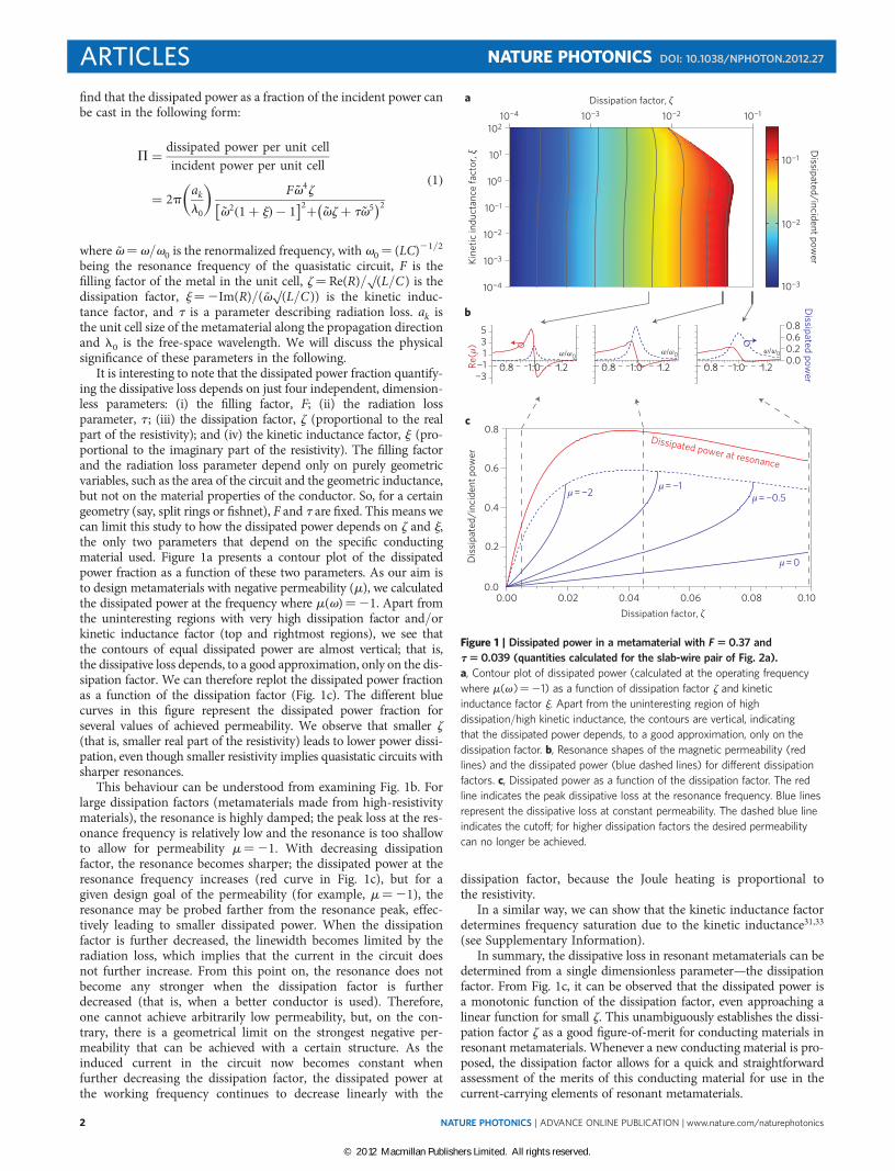
It is interesting to note that the dissipated power fraction quantify-ing the dissipative loss depends on just four independent, dimension-less parameters: (i) the filling factor, F; (ii) the radiation lossparameter, t ; (iii) the dissipation factor, z (proportional to the realpart of the resistivity); and (iv) the kinetic inductance factor, j (pro-portional to the imaginary part of the resistivity). The filling factorand the radiation loss parameter depend only on purely geometricvariables, such as the area of the circuit and the geometric inductance,but not on the material properties of the conductor. So, for a certaingeometry (say, split rings or fishnet), F and t are fixed. This means wecan limit this study to how the dissipated power depends on z and j,the only two parameters that depend on the specific conductingmaterial used. Figure 1a presents a contour plot of the dissipatedpower fraction as a function of these two parameters. As our aim isto design metamaterials with negative permeability (m), we calculatedthe dissipated power at the frequency where m(v)¼21. Apart fromthe uninteresting regions with very high dissipation factor and/orkinetic inductance factor (top and rightmost regions), we see thatthe contours of equal dissipated power are almost vertical; that is,the dissipative loss depends, to a good approximation, only on the dis-sipation factor. We can therefore replot the dissipated power fractionas a function of the dissipation factor (Fig. 1c). The different bluecurves in this figure represent the dissipated power fraction forseveral values of achieved permeability. We observe that smaller z(that is, smaller real part of the resistivity) leads to lower power dissi-pation, even though smaller resistivity implies quasistatic circuits withsharper resonances.
This behaviour can be understood from examining Fig. 1b. Forlarge dissipation factors (metamaterials made from high-resistivitymaterials), the resonance is highly damped; the peak loss at the res-onance frequency is relatively low and the resonance is too shallowto allow for permeability m¼21. With decreasing dissipationfactor, the resonance becomes sharper; the dissipated power at theresonance frequency increases (red curve in Fig. 1c), but for agiven design goal of the permeability (for example, m¼21), theresonance may be probed farther from the resonance peak, effec-tively leading to smaller dissipated power. When the dissipationfactor is further decreased, the linewidth becomes limited by theradiation loss, which implies that the current in the circuit doesnot further increase. From this point on, the resonance does notbecome any stronger when the dissipation factor is furtherdecreased (that is, when a better conductor is used). Therefore,one cannot achieve arbitrarily low permeability, but, on the con-trary, there is a geometrical limit on the strongest negative per-meability that can be achieved with a certain structure. As theinduced current in the circuit now becomes constant whenfurther decreasing the dissipation factor, the dissipated power atthe working frequency continues to decrease linearly with the
dissipation factor, because the Joule heating is proportional tothe resistivity.
In a similar way, we can show that the kinetic inductance factordetermines frequency saturation due to the kinetic inductance31,33
(see Supplementary Information).In summary, the dissipative loss in resonant metamaterials can be
determined from a single dimensionless parameter—the dissipationfactor. From Fig. 1c, it can be observed that the dissipated power isa monotonic function of the dissipation factor, even approaching alinear function for small z. This unambiguously establishes the dissi-pation factor z as a good figure-of-merit for conducting materials inresonant metamaterials. Whenever a new conducting material is pro-posed, the dissipation factor allows for a quick and straightforwardassessment of the merits of this conducting material for use in thecurrent-carrying elements of resonant metamaterials.
10−4
10−2
10−1
100
101
102
10−3
10−4 10−3 10−2
Dissipation factor, ζ
Kin
etic
ind
uct
ance
fac
tor,
ξ
a
135
−1−3
Re(μ
)
b
c
10−2
10−1
Dissip
ated/
incid
ent p
ow
er
0.00 0.02 0.04 0.06 0.08 0.10
Dissipation factor, ζ
0.0
0.2
0.4
0.6
0.8
Dis
sip
ated
/in
cid
ent
po
wer
10−1
Dissipated power at resonance
μ = −1μ = −2
μ = −0.5
μ = 0
0.8
ω/ω0
1.0 1.2 0.8
ω/ω0
1.0 1.2 0.8
ω/ω0
1.0 1.2
Dissip
ated p
ow
er
0.8
0.00.20.6
10−3
Figure 1 | Dissipated power in a metamaterial with F50.37 and
t50.039 (quantities calculated for the slab-wire pair of Fig. 2a).
a, Contour plot of dissipated power (calculated at the operating frequency
where m(v)¼21) as a function of dissipation factor z and kinetic
inductance factor j. Apart from the uninteresting region of high
dissipation/high kinetic inductance, the contours are vertical, indicating
that the dissipated power depends, to a good approximation, only on the
dissipation factor. b, Resonance shapes of the magnetic permeability (red
lines) and the dissipated power (blue dashed lines) for different dissipation
factors. c, Dissipated power as a function of the dissipation factor. The red
line indicates the peak dissipative loss at the resonance frequency. Blue lines
represent the dissipative loss at constant permeability. The dashed blue line
indicates the cutoff; for higher dissipation factors the desired permeability
We conclude that resonant metamaterials benefit from conduct-ing materials with smaller real part of the resistivity. However, whencomparing conducting materials for which samples of comparablethickness cannot be fabricated, the geometrical details in the dissi-pation factor become important. This will be essential when weinvestigate the two-dimensional conductor graphene in the nextsection. Note that we have derived the loss factor for negative-per-meability metamaterials, but it is also applicable to other metama-terials that rely on the resonant response of other polarizabilities,for example, with negative permittivity and giant chirality.
Graphene at optical frequenciesGraphene is a two-dimensional system in which electric current iscarried by massless quasiparticles34,35. We have seen above that forlow-loss resonant metamaterials, we need conducting materialswith a small real part of the resistivity (to allow for largecurrents) and small imaginary part of the resistivity (to avoidsaturation of the resonance frequency). Band structure calculationsand recent experiments indicate that minimal resistivity in themid-infrared and visible band is achieved for charge-neutralgraphene, where the surface conductivity equals the universalvalue s0¼ pe2/2h (refs 36–38).
For the slab-wire pair of Fig. 2a, we have calculated the dissipa-tion factor (Fig. 2b) and the kinetic inductance factor (Fig. 2c) forgold and graphene. Gold slab-wire pairs can provide negative per-meability (m¼21) if the lattice constant is larger than 0.15 mm(full line). For smaller lattice constants (dashed line), the dissipationfactor increases above the cutoff at which negative permeabilitycannot be achieved. The dissipation and kinetic inductance factorsfor graphene are several orders of magnitude larger than for gold.The dissipation factor of graphene is 1,200, which is deep into thecutoff region of Fig. 1a, where the losses are tremendous and themagnetic resonance is highly damped. In addition, the dissipationfactor of graphene is scale-invariant; graphene cannot be made abetter conductor by making the slab-wire pair larger. We must con-clude that graphene is not conducting well enough for use in res-onant metamaterials at infrared and visible frequencies.
This observation might not be so surprising given that recentresults have demonstrated the optical transmittance through afree-standing graphene sheet to be more than 97%; that is, graphenehas a fairly small interaction cross-section with optical radiation38.Many works have ascribed a high bulk conductivity to gra-phene—obtained by dividing its surface conductivity by the ‘thick-ness’ of the monatomic layer. This is true, but irrelevant formetamaterial purposes, where it is the total transported currentthat is important. However, graphene might still be useful for meta-materials when it is combined with a metallic structure39.
There has been recent interest in using graphene as a platform forSPPs20,21,40,41. For plasmonics, it is desirable to work with biased
graphene, because it has much larger kinetic inductance [Im(s)]than charge-neutral graphene. From Supplementary Fig. 4a, wesee that biased graphene indeed supports SPPs with wavelengthsmuch smaller than the free-space wavelength. At 30 THz, forexample, the wavelength of SPPs is 0.2 mm. Graphene may thusallow for the manipulation of surface plasmons on a micrometrescale at infrared frequencies. In addition, these SPPs are excellentlyconfined to the graphene surface with submicrometre lateral decaylengths (Supplementary Fig. 4b).
To minimize the loss, we can work in the frequency window justbelow the threshold of interband transitions where the Druderesponse of the free electrons is small and the interband transitionsare forbidden due to Pauli blocking. The effect of dissipation onSPPs can be best measured by the ratio of their propagation lengthand wavelength. Figure 3 plots this ratio for gold (yellow curve) andgraphene (black curve), calculated from experimental conductivitydata obtained by Li et al.36. The propagation length is at best of theorder of one SPP wavelength for strongly biased graphene in the infra-red. One might object that cleaner graphene samples with smallerRe(s) might be fabricated in the future. Therefore, as a best-case scen-ario for SPPs on graphene, we also determined the SPP propagationlength based on theoretical data for clean graphene taking intoaccount electron–electron interactions42,43, which fundamentallylimit the conductivity of graphene. We find slightly improved propa-gation lengths (red curve), but not larger than three SPP wavelengths.
Kin
etic
ind
uct
ance
fact
or,
ξ
10−4
10−2
100
102
cb
10−4
10−2
100
102
0.2 0.5 1.0 2.0 5.0 10.0
Lattice constant (μm)
0.1
a
Gold
Graphene
Gold
Graphene
0.2 0.5 1.0 2.0 5.0 10.0
Lattice constant (μm)
0.1
w
E
H
l
tm
tk
Dis
sip
atio
n f
acto
r, ζ
Figure 2 | Comparison between the loss factors and kinetic inductance factors of charge-neutral graphene and gold. a, The slab-wire pair used as an
example of a magnetic metamaterial (parameters provided in Methods). b, Dissipation factors for the slab-wire pair made from graphene and from gold.
c, Kinetic inductance factors for the slab-wire pair made from graphene and from gold. (The full lines indicate that the structure can provide negative
permeability (m¼21); the dashed lines indicate that the structure is beyond the cutoff and the resonance is too shallow to obtain m¼21.).
100
102
104
10−2
10−4
10 100 1,000
Frequency (THz)
Pro
pag
atio
n le
ng
th/
SP
P w
avel
eng
th
AuGraphene (71 V, exp.)
Graphene(71 V, clean, theory)
Figure 3 | Comparison of the plasmonic properties of graphene and gold.
The results for gold are for a 30-nm-thick film at room temperature. The
results for graphene are for strongly biased graphene calculated from
experimental (exp.) conductivity data (from ref. 36) and calculated from
theoretical conductivity data that incorporates electron–electron interactions
(from ref. 42). Calculations based on theoretical data for the conductivity of
graphene serve as a best-case scenario, because electron–electron
Such short propagation lengths will probably be detrimental to mostplasmonic applications.
High-temperature superconductors at terahertz frequenciesA successful approach towards low-loss microwave metamaterials isthe use of type-I superconductors44. The microwave resistivity(5 GHz) of niobium sputtered films, for example, is 1.6×10213Vm at 5 K, roughly five orders of magnitude smaller thansilver. Unfortunately, this approach is rendered ineffective at tera-hertz frequencies, because terahertz photons have sufficientenergy to break up the Cooper pairs that underlie the superconduct-ing current transport. It has therefore been suggested to use high-temperature superconductors with a larger bandgap.
We know from the above analysis that we must compare the res-istivity, which is the geometry-independent part of the dissipationfactor (we can leave out the geometrical terms here because metallicand superconducting films of the same thickness can be fabricated).Figure 4 presents a comparison of silver (data from ref. 45) andyttrium barium copper oxide (YBCO; data from ref. 46). Weobserve that from 0.5 THz to 2.5 THz, both the real part of the res-istivity (dissipation) and the imaginary part (kinetic inductance) ofYBCO are significantly larger than those of silver. We therefore con-clude that high-Tc superconductors do not perform better than
silver as conducting materials at terahertz frequencies. The reasonfor the high resistivity values of YBCO is the specific current trans-port process occurring in a superconductor. For direct current(d.c.), the electrons in the normal state are completely screened bythe superfluid—hence its zero d.c. resistivity. At non-zero frequen-cies, however, the screening is incomplete because of the finite massof the Cooper pairs. The lossy electrons in the normal state thereforecontribute to the conductance. Also, in type-II superconductors, thesuperfluid has loss mechanisms of its own, like flux creep. Botheffects lead to a non-zero resistivity, even at frequencies wellbelow the bandgap of the superconductor44.
For the sake of completeness, we mention that the plasma fre-quencies of superconductors are not much larger than those ofgold; in other words, they have similar kinetic inductance. So, at fre-quencies below the bandgap of the superconductor, the dispersionrelation of surface plasmons is very close to the light line and super-conductors do not support well-confined SPPs.
Comparative study of metals and conducting oxidesIn Fig. 5, we have classified a variety of conducting materialsaccording to their plasma frequency and collision frequency. Thecollision frequency takes into account all scattering from theconducting electronic states (electron–phonon scattering, interband
Im(r
esis
tivi
ty)
(S m
−1 )
10−9
10−8
10−7
10−6
Re(
resi
stiv
ity)
(S
m−
1 )
ba
10−8
10−7
0.5 1.0 1.5 2.0 2.5
Frequency (THz)
10−6
Ag
YBCO, 10 K
YBCO, 50 K
Ag
YBCO, 10 K
YBCO, 50 K
0.5 1.0 1.5 2.0 2.5
Frequency (THz)
Figure 4 | Comparison of the superconductor YBCO at 10 and 50 K (below the critical temperature of 80 K) with silver at room temperature. a, Real part
of the resistivity as a measure of the dissipative loss. b, Imaginary part of the resistivity as a measure of kinetic inductance.
10−8 Ω m
10−7 Ω m
10−6 Ω m
10
100
1,000
10,000
1,000
Co
llisi
on
freq
uen
cy (
TH
z)
Plasma frequency (Trad s−1)
2,000 10,000 20,000 30,0007,000
10−6 Ω m
10−5 Ω m
10−4 Ω m
AgMW IR Vis
Au
Cu
Al
Li
Na
KAu
LiAg
Pd
Be
ZrN
ITO
Al:ZnO
Cr
Pt
Ir
Ag
Au
Cu
Al
Li
Na
KAu
LiAg
Pd
Be
ZrN
ITO
Al:ZnO
Cr
Pt
Ir
Ag
Au
Cu
Al
Li
Na
KAu
LiAg
Pd
Be
ZrN
ITO
Al:ZnO
Cr
Pt
Ir
Figure 5 | Overview of conducting materials classified according to their plasma frequency and collision frequency. The different symbols indicate different
materials (see key). The collision frequency takes into account all scattering from the conducting electronic states (electron–phonon scattering, interband
transitions and so on) and therefore depends upon frequency. Blue symbols indicate material properties at microwave (MW) frequencies, red symbols in the
infrared (IR, 1.55mm), and green symbols in the visible (Vis, 500 nm). Oblique lines indicate a constant real part of the resistivity and therefore equal loss
performance in metamaterials according to our analysis.
transitions and so on) and therefore depends on frequency. Formost materials, the conductivity in the microwave band (bluesymbols in Fig. 5) is dominated by electron–phonon scattering,although interband transitions may already contribute significantly.At higher frequencies, in the infrared band (red symbols) and thevisible band (green symbols), the interband transition scatteringbecomes larger, in particular close to frequencies matching a tran-sition with high density of states.
At microwave frequencies (blue symbols in Fig. 5), silver andcopper have the smallest resistivity; copper is frequently used forits excellent compatibility with microwave technology. Transitionmetals such as gold, aluminium, chromium and iridium stillperform well. The dissipation factors obtained at microwave fre-quencies are very small and losses in the metals are typicallymodest (in fact the main loss channel is relaxation losses in thedielectric substrates). In the infrared (red symbols), the resistivityof copper is increased by a factor of ten due to interband transitionsat 560 nm. The dissipation factors at infrared frequencies are muchhigher not only due to higher resistivity, but also due to the geo-metrical scaling of the dissipation factor as shown in Fig. 2b. Goldperforms better than copper in the infrared and is easy to handleexperimentally. The reader might notice we have two data pointsin Fig. 5 for gold at 1.55 mm; we believe this disparity originatesfrom different grain sizes, which emphasizes the importance ofsample preparation. The best conducting material with the lowestresistivity now becomes silver, due to its lowest interband transitionsbeing in the ultraviolet (308 nm). We found that ZrN performssimilarly to gold. When further scaling down metamaterials foroperation in the visible (green symbols), the resistivity of most ofthe abovementioned metals becomes prohibitively high47 anddissipative losses become too high to obtain, for example, negativepermeability. The only reasonably performing metal in thevisible is silver.
Finding new materials with smaller optical resistivity could havean important impact on the field of metamaterials. We thereforeanalysed a number of recently proposed alternative conductingmaterials, for example, transparent conducting oxides such asindium tin oxide and Al:ZnO. We find they have a microwave res-istivity (blue symbols, Fig. 5) already two or more orders of magni-tude larger than the optical resistivity of silver. Thus, we can rule outthese materials—just as for graphene (analysed above), they interacttoo weakly with light. Alkali metals suffer less from interbandtransitions (compare in Fig. 5 the change in collision frequencyfrom blue� red� green for lithium/sodium versus copper).Unfortunately, their intraband collision frequency is significantlylarger and they tend to have a smaller plasma frequency, increasingthe average energy lost in each collision. There has also been recentinterest in alkali–noble intermetallics with the motivation of com-bining the low intraband resistivity of the noble metals with thereduced interband transition contribution of the alkali metals48.Two characteristic examples are KAu and LiAg. KAu (opendiamond symbols in Fig. 5) has its interband transitions far in theultraviolet and its resistivity increases only slightly from the micro-wave through the visible; however, its small plasma frequency leadsto a relatively large resistivity. On the other hand, LiAg (open circlesin Fig. 5) has a larger plasma frequency, but performs badly athigher frequencies because of significant interband scattering.These examples show, nevertheless, the possibility of bandengineering to tune the resistivity of alloys49. We believe it isworth continuing the research effort to develop better conductingmaterials, because of the considerable improvement such materialswould bring.
MethodsThe comparative study of conducting materials for resonant metamaterialspresented in this work is based on the fact that the dissipative loss in normalized
units can be written as a function of two material-dependent parameters—thedissipation factor and the kinetic inductance factor—as expressed in equation (1).This equation is obtained from a quasistatic analysis assuming the conductiveelements of the metamaterial to be smaller than the free-space wavelength of theincident radiation. Special attention was paid to the radiation resistance, as itsneglect would lead to a circuit model where the dissipated power could becomelarger than the incident power. The radiation resistance term is obtained from anear-field expansion of the magnetic fields generated by the circuit current, which isagain justified by the subwavelength dimensions of the circuit. The details of thederivation of equation (1) are given in the Supplementary Methods andSupplementary Fig. 1.
Throughout the manuscript, we exemplified the classification procedure forconducting materials using a particular metamaterial constituent—the slab-wirepair. Nevertheless, the same procedure is applicable for any other metamaterialconsisting of subwavelength conducting elements. The slab-wire pair (shown inFig. 2a) had dimensions of l¼ 2.19ak , w¼ 0.47ak , t¼ 0.5ak , tm¼ 0.25ak (tm is ofcourse not relevant for two-dimensional conductors such as graphene), aE¼ 2.97akand aH¼ 2.19ak. The relative permittivity of the substrate was 1r¼ 2.14.
We used simple expressions for the parallel-plate capacitor and the solenoidinductance, which were shown to provide an adequate description for theslab-wire pair31:
C = 101rwl
t, L = m0
lt
aH, R =
r
tm
2l
w(2)
The area enclosed by the circuit is
A = lt (3)
This is sufficient to calculate the geometry-dependent term of the dissipation andkinetic inductance factors,
z =Re r
( )
tm
���
10m0
√
���
1r√ 2l
���
aH√
t��
w√
j =Im r
( )
tm
1
v
���
10m0
√
���
1r√ 2l
���
aH√
t��
w√
(4)
The filling factor F and the radiation loss parameter t can also be calculated:
F = m0A2N/L =
lt
akaE= 0.37
t =1
6p
�������
m0/10√
�����
L/C√ v4
0A2
c4=
1
6p
1
13/2r
a5/2H t
l2w3/2= 0.039
(5)
Calculation of the dissipation factor and the kinetic inductance factor for a slab-wirepair made of graphene needs special consideration because of the two-dimensionalnature of the current transport. The geometry-dependent terms in z and j arecalculated in the previous paragraph. The resistivity was obtained usingexperimental data from Li et al.36. The real part of the measured surface conductivityof graphene to very good approximation is equal to s0¼ pe2/(2h)¼ 6.08×1025 S m21. The imaginary part is more than 10 times smaller and, as aconsequence, there is significant uncertainty in its measured value. We thereforefitted two Drude functions to the experimental data: (i) the first provides a lowerbound to the measured imaginary part of the conductivity and (ii) the other providesan upper bound (Supplementary Fig. 3). Note that these fits are phenomenologicaland are unrelated to the Drude-like behaviour of the intraband carriers, because thecurrent transport is dominated by interband carriers in the infrared and the visible.
The uncertainty in the imaginary part of the conductivity does not affect thevalue of the dissipation factor, because
Re(r) =Re(s)
Re(s)2 + Im(s)2≈
1
Re(s)(6)
However, it does lead to uncertainty in the kinetic inductance factor, indicated bythe error bars in Fig. 2c. The fitted Drude functions are finally used in equations (4)to determine the dissipation factor and the kinetic inductance factors, respectively.
The properties of an SPP (≏exp[i(bz2vt)]) propagating in the z-direction ongraphene (dispersion relation in Supplementary Fig. 4a, lateral confinement lengthin Supplementary Fig. 4b, and propagation length in Fig. 3) were calculated from thedispersion relation derived in ref. 20,
where h0 is the characteristic impedance of free space. The SPP wavelength isobtained from lSPP¼ 2p/|Re(b)|, the propagation length by 1/|Im(b)|, and thelateral decay length by 1/Re[
√(b2 − (v/c)2)]. For the conductivity of graphene, s‖ ,
we used experimental data for strongly biased (Vbias¼ 71 V) graphene from ref. 36.In addition, we have used the theoretical model by Peres et al. for the conductivity ofgraphene to calculate the propagation length of a very clean graphene sample42. Thistheoretical data ignores extrinsic scattering such as impurities (which couldpotentially be removed in cleaner samples), but does account for electron–electroninteractions (an intrinsic effect that cannot be removed).
The comparative analysis of metals and conductive oxides in Fig. 5 is based onexperimental data from several sources. In Supplementary Table 1, we list the plasmafrequency, the collision frequency and the resistivity of the metals and theconducting oxides contained in Fig. 5. References for the experimental data pointsare also provided in Supplementary Table 1.
Received 16 August 2011; accepted 24 January 2012;
published online 4 March 2012
References1. Smith, D. R., Pendry, J. B. & Wiltshire, M. C. K. Metamaterials and negative
refractive index. Science 305, 788–792 (2004).2. Shalaev, V. M. Optical negative-index metamaterials. Nature Photon. 1,
41–48 (2006).3. Soukoulis, C. M. & Wegener, M. Optical metamaterials—more bulky and less
lossy. Science 330, 1633–1634 (2010).4. Yen, T. J. et al. Terahertz magnetic response from artificial materials. Science
303, 1494–1496 (2004).5. Linden, S. et al. Magnetic response of metamaterials at 100 terahertz. Science
306, 1351–1353 (2004).6. Enkrich, C. et al. Magnetic metamaterials at telecommunication and visible
frequencies. Phys. Rev. Lett. 95, 203901 (2005).7. Shelby, R. A., Smith, D. R. & Schultz, S. Experimental verification of a negative
index of refraction. Science 292, 77–79 (2001).8. Zhang, S. et al. Experimental demonstration of near-infrared negative index
metamaterials. Phys. Rev. Lett. 95, 137404 (2005).9. Shalaev, V. M. et al. Negative index of refraction in optical metamaterials. Opt.
Lett. 30, 3356–3358 (2005).10. Plum, E. et al.Metamaterial with negative index due to chirality. Phys. Rev. B 79,
035407 (2009).11. Economou, E. N. Surface plasmons in thin films. Phys. Rev. 182, 539–554 (1969).12. Boardman, A. D. Electromagnetic Surface Modes (Wiley, 1982).13. Maier, S. A. & Atwater, H. A. Plasmonics: localization and guiding of
electromagnetic energy in metal/dielectric structures. J. Appl. Phys. 98,011101 (2005).
14. Gramotnev, D. K. & Bozhevolnyi, S. I. Plasmonics beyond the diffraction limit.Nature Photon. 4, 83–91 (2010).
15. Catchpole, K. R. & Polman, A. Plasmonic solar cells. Opt. Express 16,21793–21800 (2008).
16. Soukoulis, C. M., Zhou, J., Koschny, T., Kafesaki, M. & Economou, E. N. Thescience of negative index materials. J. Phys. Condens. Matter 20, 304217 (2008).
17. Bozhevolnyi, S. I., Volkov, V. S., Devaux, E. & Ebbesen T. W. Channel plasmon-polariton guiding by subwavelength metal grooves. Phys. Rev. Lett. 95,046802 (2005).
18. Kolomenski, A., Kolomenskii, A., Noel, J., Peng, S. & Schuessler, H. Propagationlength of surface plasmons in a metal film with roughness. Appl. Opt. 48,5683–5691 (2009).
19. Boltasseva, A. & Atwater, H. A. Low-loss plasmonic metamaterials. Science 331,290–291 (2011).
20. Vakil, A. & Engheta, N. Transformation optics using graphene. Science 332,1291–1294 (2011).
21. Koppens, F. H. L., Chang, D. E. & Garcıa de Abajo, F. J. Graphene plasmonics:a platform for strong light–matter interactions.Nano Lett. 11, 3370–3377 (2011).
22. Chen, H.-T. et al. Tuning the resonance in high-temperature superconductingterahertz metamaterials. Phys. Rev. Lett. 105, 247402 (2010).
23. Pendry, J. B., Holden, A. J., Robbins, D. J. & Stewart, W. J. Magnetism fromconductors and enhanced nonlinear phenomena. IEEE Trans. Microwave TheoryTech. 47, 2075–2084 (1999).
24. Gorkunov, M., Lapine, M., Shamonina, E. & Ringhofer, K. H. Effective magneticproperties of a composite material with circular conductive elements. Eur.Phys. J. B 28, 263–269 (2002).
25. Engheta, N. Circuits with light at nanoscales: optical nanocircuits inspired bymetamaterials. Science 317, 1698–1702 (2007).
26. Koschny, T., Kafeski, M., Economou, E. N. & Soukoulis, C. M. Effective mediumtheory of left-handed materials. Phys. Rev. Lett. 93, 107402 (2004).
27. Zhang, S., Genov, D. A., Wang, Y., Liu, M. & Zhang, X. Plasmon-inducedtransparency in metamaterials. Phys. Rev. Lett. 101, 047401 (2008).
28. Papasimakis, N., Fedotov, V. A., Zheludev, N. I. & Prosvirnin, S. L. Metamaterialanalog of electromagnetically induced transparency. Phys. Rev. Lett. 101,253903 (2008).
29. Tassin, P., Zhang, L., Koschny, Th., Economou, E. N. & Soukoulis, C. M. Low-loss metamaterials based on classical electromagnetically induced transparency.Phys. Rev. Lett. 102, 053901 (2009).
30. Liu, N. et al. Plasmonic analogue of electromagnetically induced transparency atthe Drude damping limit. Nature Mater. 8, 758–762 (2009).
31. Penciu, R. S., Kafesaki, M., Koschny, Th., Economou, E. N. & Soukoulis, C. M.Magnetic response of nanoscale left-handed metamaterials. Phys. Rev. B 81,
235111 (2010).32. Luan, P. Power loss and electromagnetic energy density in a dispersive
metamaterial medium. Phys. Rev. B 80, 046601 (2009).33. Zhou, J. et al. Saturation of the magnetic response of split-ring resonators at
optical frequencies. Phys. Rev. Lett. 95, 223902 (2005).34. Castro Neto, A. H., Guinea, F., Peres, N. M. R., Novoselov, K. S. & Geim, A. K.,
The electronic properties of graphene. Rev. Mod. Phys. 81, 109–162 (2009).35. Bonaccorso, F., Sun, Z., Hasan, T. & Ferrari, A. C. Graphene photonics and
optoelectronics. Nature Photon. 4, 611–622 (2010).36. Li, Z. Q. et al. Dirac charge dynamics in graphene by infrared spectroscopy.
Nature Phys. 4, 532–535 (2008).37. Horng, J. et al., Drude conductivity of Dirac fermions in graphene. Phys. Rev. B
83, 165113 (2011).38. Nair, R. R. et al. Fine structure constant defines visual transparency of graphene.
Science 320, 1308–1308 (2008).39. Papasimakis, N. et al. Graphene in a photonic metamaterial. Opt. Express 18,
8353–8358 (2010).40. Hanson, G. W. Dyadic Green’s functions and guided surface waves for a surface
conductivity model of graphene. J. Appl. Phys. 103, 064302 (2008).41. Jablan, M., Buljan, H. & Soljacic, M. Plasmonics in graphene at infrared
frequencies. Phys. Rev. B 80, 245435 (2009).42. Peres, N. M. R., Ribeiro, R. M. & Castro Neto, A. H. Excitonic effects in the
optical conductivity of gated graphene. Phys. Rev. Lett. 105, 055501 (2010).43. Grushin, A. G., Valenzuela, B. & Vozmediano, M. A. H. Effect of Coulomb
interactions on the optical properties of doped graphene. Phys. Rev. B 80,
155417 (2009).44. Anlage, S. M. The physics and applications of superconducting metamaterials.
J. Opt. 13, 024001 (2011).45. Ordal, M. A., Bell, R. J., Alexander, R. W., Long, L. L. & Querry, M. R. Optical
properties of fourteen metals in the infrared and far infrared: Al, Co, Cu, Au, Fe,Pb, Mo, Ni, Pd, Pt, Ag, Ti, V, and W. Appl. Opt. 24, 4493–4499 (1985).
46. Kumar, A. R. et al. Far-infrared transmittance and reflectance of YBa2Cu3O7–d
films on Si substrates. J. Heat Transfer 121, 844–851 (1999).47. Khurgin, J. B. & Sun, G., Scaling of losses with size and wavelength in
nanoplasmonics and metamaterials. Appl. Phys. Lett. 99, 211106 (2011).48. Blaber, M. G., Arnold, M. D. & Ford, M. J. Designing materials for plasmonic
systems: the alkali-noble intermetallics. J. Phys. Condens. Matter 22,095501 (2010).
49. Bobb, D. A. et al. Engineering of low-loss metal for nanoplasmonic andmetamaterials applications. Appl. Phys. Lett. 95, 151102 (2009).
AcknowledgementsWork at Ames Laboratory was partially supported by the US Department of Energy, Office
of Basic Energy Science, Division of Materials Sciences and Engineering (Ames Laboratory
is operated for the US Department of Energy by Iowa State University under contract no.
DE-AC02-07CH11358) (theoretical studies) and by the USOffice of Naval Research (award
no. N00014-10-1-0925, study of graphene). Work at FORTH was supported by the
European Community’s FP7 projects NIMNIL (grant agreement no. 228637, graphene)
and ENSEMBLE (grant agreement no. 213669, study of oxides). P.T. acknowledges a
fellowship from the Belgian American Educational Foundation.
Author contributionsP.T., T.K. and C.M.S. conceived the strategy of comparing conducting materials for
metamaterials and plasmonics. P.T. assembled input data and P.T and T. K. performed the
calculations. All authors were involved in interpretation of the results. P.T. wrote the paper
and all authors commented on the manuscript at all stages.
Additional informationThe authors declare no competing financial interests. Supplementary information
accompanies this paper at www.nature.com/naturephotonics. Reprints and permission
information is available online at http://www.nature.com/reprints. Correspondence and
requests for materials should be addressed to P.T.
Supplementary Figure 1 | A quasistatic metallic circuit. The curved lines are electric field lines along which the contour integral in equation (S2) must be integrated. The field lines follow the current density in the metal and the displacement field in the gap.
The right-hand side of equation (S2) contains a contribution from the incident field as well
as a contribution from the magnetic field generated by the current in the circuit:
inc circuit
d d dd d d .
d d dt t t− ⋅ = − ⋅ − ⋅∫∫ ∫∫ ∫∫Ǻ S Ǻ S Ǻ S (S4)
Because the circuit is smaller than the wavelength, we can assume the incident magnetic
field is constant over the circuit, such that the contribution from the incident field equals
( )in 0 0c
d dcos( )d
d,
dA
tt
tHμ ω− ⋅ = −∫∫Ǻ S (S5)
where A is the area enclosed by the circuit and H0 is the magnetic field amplitude of the
incident wave.
What remains is the contribution from the magnetic induction field generated by the current
in the circuit. Again in the quasistatic approximation and after a second differentiation with
respect to time, this leads to the circuit equation with the self-inductance term:
( )2 2
0 02 2
d d 1 d dcos( ) .
d d d d
I IL R I H t
t t C tA
tμ ω+ + = − = −E
(S6)
This is Kirchoff's equation describing the electrical current, I, flowing in the metallic circuit
of each meta-atom, driven by the external time-dependent magnetic field of an incident
electromagnetic wave. A is the area enclosed by the circuit, H0 the magnetic field amplitude
of the incident wave, and Ȧ the frequency of the incident wave. The inductance, L, and
capacitance, C, must be interpreted as effective values that encompass coupling between
neighbouring circuits24
. The right-hand term in equation (S6) is of course nothing else than
the electromotive force, ছ, induced in the circuit by the incident field. Solving this equation
yields a Lorentzian response function with a resonance at frequency Ȧ0 = 1/ LC and
damping factor Ȗ = R/L. If we now make the circuit from a conductive material with
increasingly high conductivity, the resistance, R, becomes smaller and the damping factor
goes to zero. The consequence is that the dissipated power at the resonance frequency
becomes arbitrarily large, even larger than the power in the incident plane wave, which is
In terms of these dimensionless parameters, the susceptibility and dissipated power loss
fraction are
( ) ( )
2
2 51 1 i
Fωχω ξ ωζ τω
= −+ − + +
## # #
(S30)
and
( ) ( )
4
diss k
222 5
inc 0
2 equation (1)1 1
P a F
P
ω ζπλ ω ξ ωζ τω
⎛ ⎞Π = = →⎜ ⎟
⎡ ⎤⎝ ⎠ + − + +⎣ ⎦
#
# # # (S31)
The dissipation factor ȗ is a dimensionless quantity determining the dissipative loss. This is
discussed in the main text (figure 1) and forms the basis for our classification of conducting
materials for use in resonant metamaterials.
Supplementary Figure 2 | Frequency redshift in a metamaterial with F = 0.37 and IJ = 0.039;
quantities are calculated for the slab-wire pair of figure 2a. a, Contour plot indicating how much the frequency at which た(の) = �1 is redshifted due to the kinetic inductance effect and the dissipation factor. The contour lines are approximately vertical, signifying that the resonance frequency depends only on the kinetic inductance factor to good approximation. The white region is the cut-off region where the resonance is too shallow to obtain negative permeability た(の) = �1. b, Resonance shapes of the magnetic permeability for kinetic inductance factors つ = 0.01 and つ = 0.3. The dissipation factor was taken as こ = 0.02. The strength of the resonance is almost unaltered by the kinetic inductance.
The kinetic inductance factor determines the saturation of the resonance frequency of
negative-permeability metamaterials when they are scaled down towards optical
frequencies33,31
. This effect is due to the contribution of the kinetic inductance of the free
electrons or, in other words, to the mass inertia of the charge carriers. This is a material
Supplementary Figure 3 | Surface conductivity of charge-neutral graphene from reference 36. Blue, dash-dotted line: real part of the surface conductivity (measured and fitted
curves coincide). Red line: measured imaginary part of the surface conductivity. Blue, dashed lines: fitted curves representing an upper and lower bound to the measured data for the imaginary part of
the surface conductivity.
Supplementary Figure 4 | Surface plasmon polaritons on graphene and gold. The results for gold are for a 30 nm thick film at room temperature. The results for graphene are for strongly biased graphene calculated from experimental conductivity data (from ref. 36) and calculated from theoretical conductivity data that incorporates electron-electron interactions (from ref. 42). a, The wavelength of a surface plasmon polariton on graphene. Around 30 THz, the wavelength of SPPs
on graphene is much smaller than the free-space wavelength Ȝ0 = 2ʌc/Ȧ. This is an immediate
consequence of the large kinetic inductance of graphene as quantified by the kinetic inductance factor shown in figure 2c. b, Lateral confinement (away from the surface) of surface plasmon polaritons. The high kinetic inductance of graphene results in very good confinement with sub-micrometer decay length at mid-infrared frequencies.
Supplementary Table 1 | Plasma frequency, collision frequency, and resistivity of the metals and conducting oxides shown in figure 5. The numbers between parentheses refer to the literature where the data were obtained from; the quantities without references have been derived by us. We note again that the collision frequency includes all possible scattering mechanisms and is therefore frequency-dependent. The following labels are used to indicate the frequency/wavelength at which the data are evaluated: GHz (1 GHz), IR (1.55 ȝm), and VIS (500 nm).