A concept for the MVD-DAQ. C.Schrader , S. Amar-Youcef, N. Bialas, M. Deveaux, I.Fröhlich, J. Michel, B. Milanovic, C. Müntz, S. Seddiki, J. Stroth, T. Tischler, B. Wiedemann. C.Schrader; April 2010 , CBM Collaboration Meeting. Outline:. Requirements on the prototype - PowerPoint PPT Presentation
17
Institute for Nuclear Physics, University of Frankfurt Institute for Nuclear Physics, University of Frankfurt 1 A concept for the MVD-DAQ C.Schrader , S. Amar-Youcef, N. Bialas, M. Deveaux, I.Fröhlich, J. Michel, B. Milanovic, C. Müntz, S. Seddiki, J. Stroth, T. Tischler, B. Wiedemann C.Schrader; April 2010, CBM Collaboration Meeting
Transcript
Ins
titut
e fo
r N
ucle
ar P
hysi
cs, U
nive
rsity
of F
rank
furt
Ins
titut
e fo
r N
ucle
ar P
hysi
cs, U
nive
rsity
of F
rank
furt
1
A concept for theMVD-DAQ
C.Schrader, S. Amar-Youcef, N. Bialas, M. Deveaux, I.Fröhlich, J. Michel, B. Milanovic, C. Müntz, S. Seddiki, J. Stroth,
T. Tischler, B. Wiedemann
C.Schrader; April 2010, CBM Collaboration Meeting
Ins
titut
e fo
r N
ucle
ar P
hysi
cs, U
nive
rsity
of F
rank
furt
Ins
titut
e fo
r N
ucle
ar P
hysi
cs, U
nive
rsity
of F
rank
furt
2C.Schrader; April 2010, CBM Collaboration Meeting
Outline:
1. Requirements on the prototype
2. The prototype sensor (Mimosa26)
3. The prototype readout concept
based on existing hardware
4. Network concept
5. Status and conclusion
Ins
titut
e fo
r N
ucle
ar P
hysi
cs, U
nive
rsity
of F
rank
furt
C.Schrader; April 2010, CBM Collaboration Meeting
The Demonstrator
analogue output
sync. signals
demo-AUX
MAPS add-on board
Trb2(TRBnet)
file server
monitoring
data transfer: I/O-card
data transfer: OP
-link
or
Beam test @ Cern-SPSNov 2009
Demonstrator project
accomplished
See talk of Samir
3
Ins
titut
e fo
r N
ucle
ar P
hysi
cs, U
nive
rsity
of F
rank
furt
C.Schrader; April 2010, CBM Collaboration Meeting
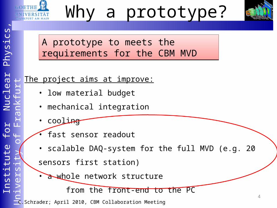
The project aims at improve:
• low material budget
• mechanical integration
• cooling
• fast sensor readout
• scalable DAQ-system for the full MVD (e.g. 20 sensors first station)
• a whole network structure
from the front-end to the PC
Why a prototype?
A prototype to meets the requirements for the CBM MVD A prototype to meets the requirements for the CBM MVD
4
Ins
titut
e fo
r N
ucle
ar P
hysi
cs, U
nive
rsity
of F
rank
furt
C.Schrader; April 2010, CBM Collaboration Meeting
M. Deveaux, ULISI kick-off meeting, GSI, Feb. 17-18, 2010
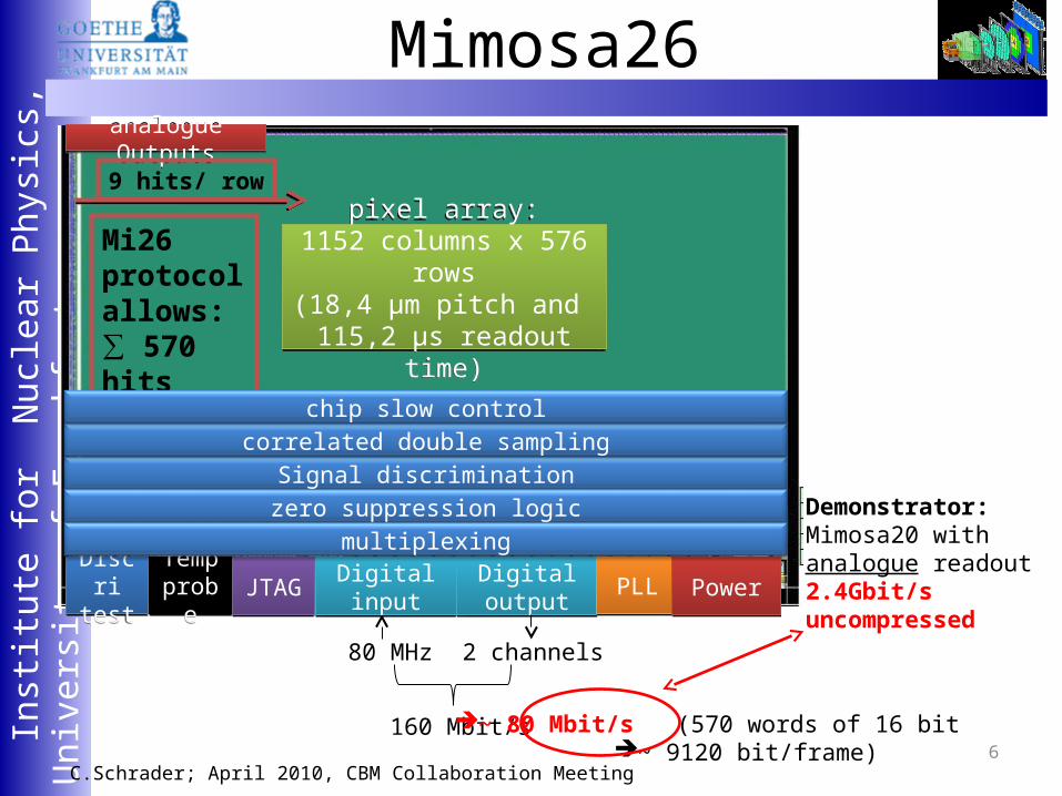
Mimosa26 offers:• logic for data reduction• huge pixel array (form factor for the final MVD)• multiplexer for faster readout• inspiration for the final MVD sensor (MimoSIS-1)
5
* best of
Ins
titut
e fo
r N
ucle
ar P
hysi
cs, U
nive
rsity
of F
rank
furt
C.Schrader; April 2010, CBM Collaboration Meeting
Mimosa26analogue Outputsanalogue Outputs
pixel array:1152 columns x 576 rows
(18,4 µm pitch and 115,2 µs readout time)
pixel array:1152 columns x 576 rows
(18,4 µm pitch and 115,2 µs readout time)
JTAGJTAG Digitalinput
Digitalinput
Digital outputDigital output PLLPLLTemp
probeTempprobe
Discritest
Discritest PowerPower
Signal discriminationzero suppression logic
correlated double sampling
2 channels80 MHz
160 Mbit/s ~ 80 Mbit/s (570 words of 16 bit ~ 9120 bit/frame)
9 hits/ row
Mi26 protocol allows:∑ 570 hits
multiplexingDemonstrator: Mimosa20 with analogue readout2.4Gbit/suncompressed
chip slow control
6
Ins
titut
e fo
r N
ucle
ar P
hysi
cs, U
nive
rsity
of F
rank
furt
C.Schrader; April 2010, CBM Collaboration Meeting
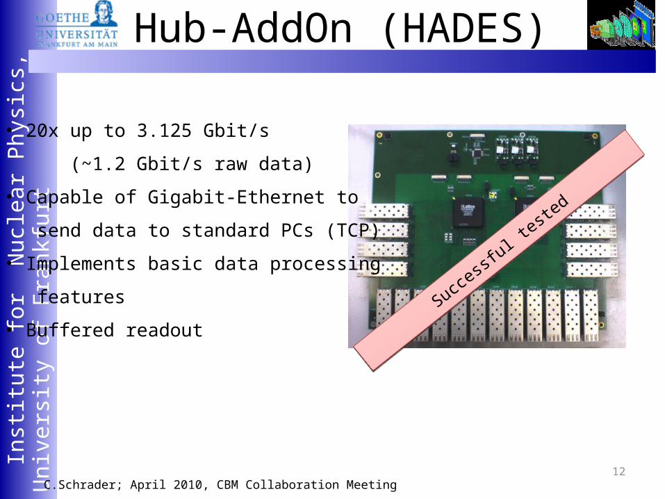
• readout board for 3x Mimosa 26• platform to study online data
specification for data reduction • compatibility with HADES DAQ
(Trb2) for testing purposes
developed by IKF electronic workshop
The add-on board with a FPGA Is mounted on the TRBv2 back side
The Trbv2 (HADES) provides a flexible add-on board concept
• high data-rate digital interface
connector (15 Gbit/s)
• FPGA configuration
• high data transfer with optical link
(2 Gbit/s)
• application process interface (API)
• power supply +5V,10A
• clock distribution
The readout boards
7
Ins
titut
e fo
r N
ucle
ar P
hysi
cs, U
nive
rsity
of F
rank
furt
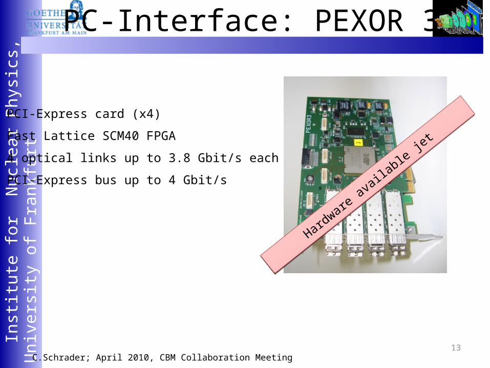
C.Schrader; April 2010, CBM Collaboration Meeting
The prototype readout
A telescope to study:• Protocol
– scalable (unique ID for 512 sensors)– time/trigger stamps (for assynchronous readout
of the sensors)– safety aspects (check- sum and data length)– data reduction (160 Mbit/s down to 80 Mbit/s)– buffered readout
• JTAG chain• Online monitoring• Beam tests
• Offline analysis/tracking (CBM-root) 2m2m
2m2m
1x Start,clk,Rst(LVDS)1x Start,clk,Rst(LVDS)
15 cm15 cm
3x D0,D1,CLK(LVDS)3x D0,D1,CLK(LVDS)
2m2m
3 stations „telescope“ vacuum
133 Mbyte/s~ 13 sensors
JTAG chainJTAG chain
control chaincontrol chain
data outputdata output
Mimosa26 Digi Aux
JTAG board
MAPS add-on
8
Ins
titut
e fo
r N
ucle
ar P
hysi
cs, U
nive
rsity
of F
rank
furt
C.Schrader; April 2010, CBM Collaboration Meeting
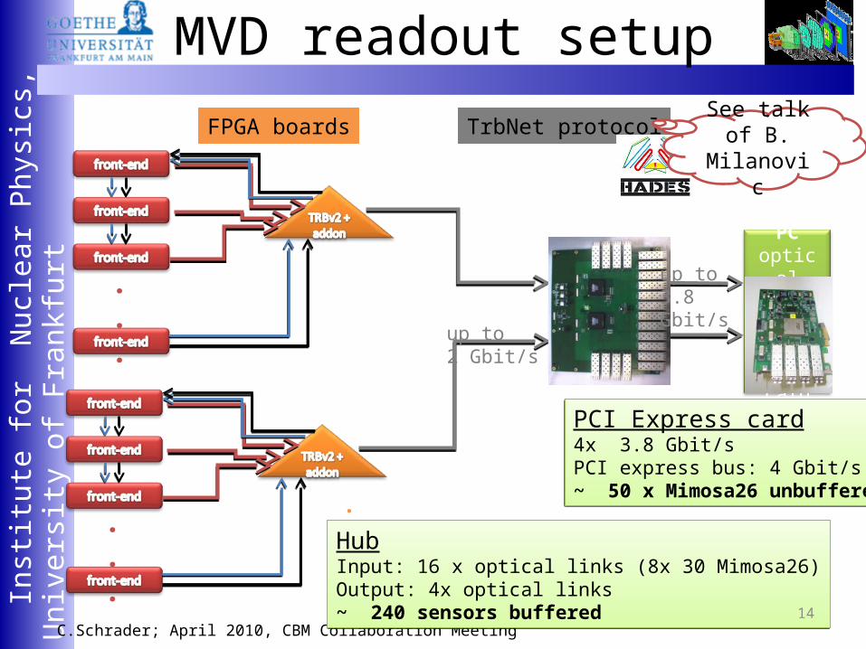
Scalable DAQ-system
To study:• Scalable system (unique ID for boards)• Board synchronisation• Repeater for signal conditioning
1x RJ451x RJ45
1x Start,clk,Rst(LVDS)1x Start,clk,Rst(LVDS)
3x D0,D1,CLK(LVDS)3x D0,D1,CLK(LVDS)
3x D0,D1,CLK(LVDS)3x D0,D1,CLK(LVDS)
MAPS add-onI/O limitation for only 3 sensors
Mimosa26 Digi Aux
JTAG board
MAPS add-on
9
Ins
titut
e fo
r N
ucle
ar P
hysi
cs, U
nive
rsity
of F
rank
furt
C.Schrader; April 2010, CBM Collaboration Meeting
Data rate of the sensors was simulated accounting for: pile-up, delta electrons, clustering,fake hits rates with the data protocols of Mimosa26
Conclusions:
Total data rate of the MVD 10 GBytes/s
First MVD station located at 5 cm
See talk ofS.Seddiki
Data rate for the MVD
Data rate of individual sensor < 2.4 Gbit/s
Data reduction on FPGA boards
10
Ins
titut
e fo
r N
ucle
ar P
hysi
cs, U
nive
rsity
of F
rank
furt
C.Schrader; April 2010, CBM Collaboration Meeting
4x LVDS JTAG3x LVDS clk/start/rst
3x LVDS D0,D1,clk
2x optical link (each 2 Gbit/s)> 30 Mimosa26/board
2x optical link (each 2 Gbit/s)> 30 Mimosa26/board
.
.
.
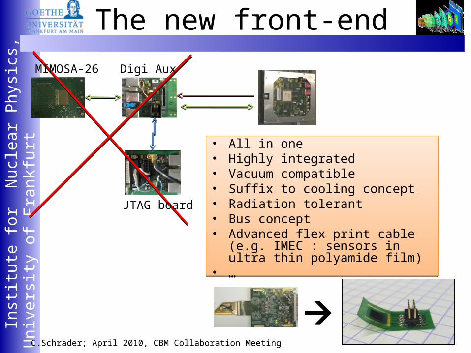
New add-on board:- chip controlling- chip mointoring- protocol for front-ends- network protocol (TrbNet)- … (telescope studies)
Trbv2:- JTAG- power supply- monitoring
digital chip data via optical link (2 Gbit/s)
2m2m
New readout board
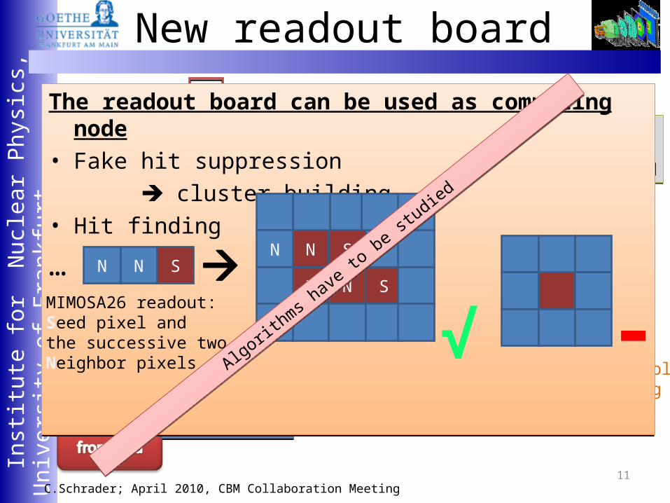
The readout board can be used as computing node• Fake hit suppression
cluster building• Hit finding
…
The readout board can be used as computing node• Fake hit suppression
cluster building• Hit finding
… N S
N N S
√ -N N S
MIMOSA26 readout:Seed pixel andthe successive two Neighbor pixels