University of Kentucky UKnowledge University of Kentucky Master's eses Graduate School 2007 A CONTROLLER AREA NETWORK LAYER FOR RECONFIGUBLE EMBEDDED SYSTEMS Nithyananda Siva Jeganathan University of Kentucky, [email protected]Click here to let us know how access to this document benefits you. is esis is brought to you for free and open access by the Graduate School at UKnowledge. It has been accepted for inclusion in University of Kentucky Master's eses by an authorized administrator of UKnowledge. For more information, please contact [email protected]. Recommended Citation Jeganathan, Nithyananda Siva, "A CONTROLLER AREA NETWORK LAYER FOR RECONFIGUBLE EMBEDDED SYSTEMS" (2007). University of Kentucky Master's eses. 484. hps://uknowledge.uky.edu/gradschool_theses/484
Transcript
University of KentuckyUKnowledge
University of Kentucky Master's Theses Graduate School
2007
A CONTROLLER AREA NETWORK LAYERFOR RECONFIGURABLE EMBEDDEDSYSTEMSNithyananda Siva JeganathanUniversity of Kentucky, [email protected]
Click here to let us know how access to this document benefits you.
This Thesis is brought to you for free and open access by the Graduate School at UKnowledge. It has been accepted for inclusion in University ofKentucky Master's Theses by an authorized administrator of UKnowledge. For more information, please contact [email protected].
Recommended CitationJeganathan, Nithyananda Siva, "A CONTROLLER AREA NETWORK LAYER FOR RECONFIGURABLE EMBEDDEDSYSTEMS" (2007). University of Kentucky Master's Theses. 484.https://uknowledge.uky.edu/gradschool_theses/484
A CONTROLLER AREA NETWORK LAYER FOR RECONFIGURABLE
EMBEDDED SYSTEMS
Dependable and Fault-tolerant computing is actively being pursued as a research area since the 1980s in various fields involving development of safety-critical applications. The ability of the system to provide reliable functional service as per its design is a key paradigm in dependable computing. For providing reliable service in fault-tolerant systems, dynamic reconfiguration has to be supported to enable recovery from errors (induced by faults) or graceful degradation in case of service failures. Reconfigurable Distributed applications provided a platform to develop fault-tolerant systems and these reconfigurable architectures requires an embedded network that is inherently fault-tolerant and capable of handling movement of tasks between nodes/processors within the system during dynamic reconfiguration. The embedded network should provide mechanisms for deterministic message transfer under faulty environments and support fault detection/isolation mechanisms within the network framework. This thesis describes the design, implementation and validation of an embedded networking layer using Controller Area Network (CAN) to support reconfigurable embedded systems. KEYWORDS: Dependable Computing, Fault Tolerance, Embedded Networks, Distributed system, Controller Area Network (CAN).
Nithyananda Siva Jeganathan
10/17/2007
A CONTROLLER AREA NETWORK LAYER FOR RECONFIGURABLE EMBEDDED SYSTEMS
By
NITHYANANDA SIVA JEGANATHAN
DR. JAMES E. LUMPP Jr.
Director of Thesis
DR.YU MING ZHANG
Director of Graduate Studies
10/17/2007
RULES FOR THE USE OF THESIS
Unpublished theses submitted for the Master’s degree and deposited in the University of
Kentucky Library are as a rule open for inspection, but are to be used only with due
regard to the rights of the authors. Bibliographical references may be noted, but
quotations or summaries of parts may be published only with the usual scholarly
acknowledgements.
Extensive copying or publication of the dissertation in whole or in part also requires the
consent of the Dean of the Graduate School of the University of Kentucky.
A library that borrows this project for use by its patrons is expected to secure the
signature of each user.
Name Date ________________________________________________________________________ ________________________________________________________________________ ________________________________________________________________________ ________________________________________________________________________ ________________________________________________________________________ ________________________________________________________________________ ________________________________________________________________________ ________________________________________________________________________
THESIS
NITHYANANDA SIVA JEGANATHAN
The Graduate School
University of Kentucky
2007
A CONTROLLER AREA NETWORK LAYER FOR RECONFIGURABLE EMBEDDED
SYSTEMS
THESIS
A thesis submitted in partial fulfillment of the requirements for the degree of Master of
Science in the College of Engineering
at the University of Kentucky
By
Nithyananda Siva Jeganathan
Lexington, KY
Director: Dr. James E. Lumpp Jr. , Professor of Electrical Engineering
Lexington, KY
2007
Dedicated to my family, friends and
to Almighty who shows me the way…
Acknowledgements
I would like to thank my advisor Dr. James E. Lumpp, Jr. for his invaluable guidance and
support, without which this work would not have been possible. I am grateful for the
motivation and the inspirations he had provided. I would also like to thank my Thesis
Committee members Dr. Henry G. Dietz and Dr. William R. Dieter not only for serving on
the committee, but also for providing me with great learning opportunities.
This work is dedicated to my loving family and to Seema for their understanding, support
and for being the guiding light of my life. Their love and sacrifices made everything possible
and words cannot express my gratitude.
I would like to thank Nate Rhodes and Niveditha for their painstaking efforts in proof-
reading of the thesis work and their valuable suggestions. Last, but not the least I thank my
friends who had motivated me and stood by me in everything.
iii
Table of Contents Acknowledgements .................................................................................................................. iii List of Figures .......................................................................................................................... vi List of Tables .......................................................................................................................... vii Chapter 1: Introduction ............................................................................................................. 8
1.1 Background ............................................................................................................... 8 1.2 Embedded Networks Overview ................................................................................ 9 1.3 Data Communication Protocols .............................................................................. 11
1.3.1 Message Oriented Protocols ........................................................................... 12 1.4 Medium Access Control (MAC) ............................................................................. 13 1.5 Ardea Run-time Environment ................................................................................. 14
1.6.1 CAN Advantages ............................................................................................ 21 1.7 Problem Statement .................................................................................................. 21
Chapter 2: CAN Protocol and Applications............................................................................ 24
2.2 CAN Protocol Specification ....................................................................................... 27 2.2.1 CAN Physical Layer ............................................................................................ 28 2.2.2 CAN Bit timing for the Physical Layer ............................................................... 28 2.2.3 CAN Error detection ............................................................................................ 36
Chapter 3: CAN Hardware ...................................................................................................... 39
3.1 CAN Hardware Properties: ........................................................................................... 39 3.1.1 CAN Controller Chips ......................................................................................... 39 3.1.2 CAN Transceiver chips ........................................................................................ 39 3.1.3 CAN Repeaters .................................................................................................... 40 3.1.4 CAN Bridges ........................................................................................................ 40 3.1.5 CAN Gateways .................................................................................................... 40
Chapter 5: CAN Performance & Reliability Tests ................................................................. 79
5.1 Background ................................................................................................................. 79 5.2 Test bench Set-up ........................................................................................................ 79
5.2.1 Steps to set up the test-bench ............................................................................... 81 5.3 CAN 2.0A/ B conformance testing ............................................................................. 82
5.3.1 Register identifier test .......................................................................................... 82 5.3.2 Unregister a Message Identifier Test ................................................................... 83 5.3.3 Send Packet Test .................................................................................................. 85 5.3.4 Receive packet module test .................................................................................. 86
References ............................................................................................................................. 114 Vita ........................................................................................................................................ 118
v
List of Figures Figure 1: Distributed system view on a UAV [2] ..................................................................... 9 Figure 2: OSI Layer Reference Architecture .......................................................................... 10 Figure 3: Node oriented communication ................................................................................ 11 Figure 4: Message oriented communication ........................................................................... 12 Figure 5: Ardea Dependency Graph model [26] ..................................................................... 16 Figure 6: IDEAnix Block diagram and Task level communication with MeRL [4] .............. 17 Figure 7: MeRL block diagram [4] ......................................................................................... 18 Figure 8: State Diagram for CAN Engine ............................................................................... 31 Figure 9: CAN Data Frame Format ........................................................................................ 32 Figure 10: CAN Remote Request Frame ................................................................................ 34 Figure 11: Error Frame Format ............................................................................................... 35 Figure 12: Block Diagram of CAN Application ..................................................................... 51 Figure 13: CAN Module block diagram ................................................................................. 52 Figure 14: Flow chart for initialization module ...................................................................... 54 Figure 15: Flow chart for Register module ............................................................................. 57 Figure 16: Flow chart for Unregister module ......................................................................... 62 Figure 17: Flow chart for Send Message Module ................................................................... 66 Figure 18: Translation Module block Diagram ...................................................................... 71 Figure 19: Flowchart for CAN ISR functionality ................................................................... 74 Figure 20: Block diagram for ENDURA test set up ............................................................... 80 Figure 21: Test Bench Setup for ENDURA layer testing ....................................................... 80 Figure 22: Test bench set up (a closer look) ........................................................................... 81 Figure 23: Bandwidth Graph for Packet rate Vs Packets dropped ......................................... 90 Figure 24: Block diagram representing different times measured in Latency tests ................ 93 Figure 25: Timing diagram for receiving a packet ................................................................. 94 Figure 26: Timing diagram for Sending packet ...................................................................... 95 Figure 27: Test Register Details ........................................................................................... 109
vi
vii
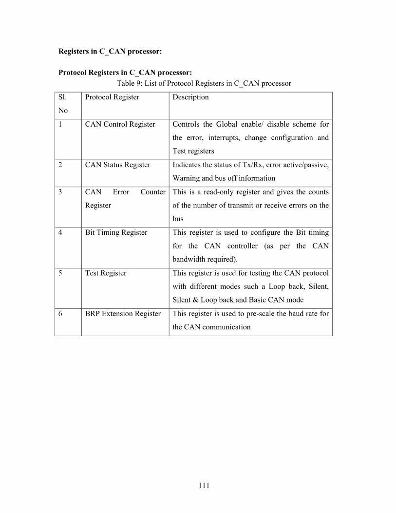
List of Tables Table 1: Design matrix for the embedded networks .............................................................. 20 Table 2: CAN frame format for a basic CAN 2.0A frame ...................................................... 33 Table 3: Bandwidth Analysis report for 100ms tick delay ..................................................... 88 Table 4: Bandwidth Analysis report for 10ms tick delay ....................................................... 89 Table 5: Bandwidth Analysis with number of packets sent over time ................................... 90 Table 6: Reliability test data after continuous run for 40 hours ............................................. 97 Table 7: Sporadic Test data for CAN ..................................................................................... 98 Table 8: Test Register Bits .................................................................................................... 109 Table 9: List of Protocol Registers in C_CAN processor ..................................................... 111 Table 10: List of Interface Registers in C_CAN processor .................................................. 112 Table 11: List of Message handler Registers in C_CAN processor ..................................... 113
Chapter 1: Introduction This chapter provides a background and introduction to the problem of providing a
networking layer to support reconfigurable systems, embedded network architectures,
data communication protocols, media access control logics are discussed. The motivation
for the thesis is discussed along with the different embedded networks options and
motivation for the choice of Controller Area Network (CAN) as the desired embedded
network. Finally the goals for the system to be developed are described in detail.
1.1 Background Dependable and Fault-tolerant computing is being actively pursued as a research area for
deployment in safety-critical applications where guaranteed functional operations of
system is paramount. The system should provide reliable services based on its functional
design and this key requirement is the motivation for implementing fault-tolerant
techniques in system. A Fault-tolerant system should be capable of detecting faults/
errors in the system and also provide minimal services in case of recoverable errors or
degrade gracefully in case of failures. Any distributed system depends on a network
mechanism for establishing communication between the different nodes and for a
reconfigurable distributed architecture, the embedded network should provide
mechanisms for deterministic message transfer under faulty environments and support
fault detection/isolation mechanisms within the network framework.
This thesis research work presents an implementation of an Embedded Network Driver
for Use on Reconfigurable Architectures (ENDURA) that supports fault-tolerant
mechanisms and can be integrated into any reconfigurable architecture as a network
layer. Controller Area Network is a differential signaling serial bus that was developed by
Robert Bosch GmbH for deployment as a system bus in Automobiles. For analyzing the
efficiency of the ENDURA implementation using CAN, a typical safety-critical
distributed system using an Unmanned Aerial Vehicle (UAV) will be considered as an
example where required. Figure 1 shows the system view for a distributed UAV system.
The Tiny Interface Module (TIM) processor boards [2] are embedded on servos and
8
mounted on the wings and the ailerons. The processor boards are connected through a
CAN bus that provides the communication mechanism for the UAV system.
Figure 1: Distributed system view on a UAV [2]
The other CAN applications that are used in Small vehicles (Light Electric Vehicles),
Marine applications (SeaCAN, NAUTILE) and Space applications (SOFIA, SMART-1)
are discussed in detail in Chapter 2.
1.2 Embedded Networks Overview An overview of the embedded networks is provided in this section. The nodes in a
network can communicate with each other or nodes outside their network through a
variety of software architecture models and physical layers (PHY). Two of the most
popular software architectures in use are the Transfer Control Protocol (TCP)/Internet
Protocol (IP) suite and the International Standards Organization (ISO)/Open Systems
Interconnection (OSI) Reference model (also known as the seven layer ISO/OSI
Reference model) [28].
The TCP/IP model was developed by the Department of Defense (DoD) to establish
connections between nodes of different types within different networks [26] . The TCP/IP
model was designed to provide guaranteed delivery of information between systems and
9
includes a sliding window protocol controlled by congestion control mechanisms [27].
The TCP/IP model led to the interconnection of networks and to the origin of the Internet.
The main reference for most of the present embedded networks protocol specifications is
the ISO/OSI Reference model [28]. It is devised by the International Standards
Organization to support open networks communications and also to encapsulate the
existing interconnection standards within the ISO reference model. The model does not
define the exact implementation methodologies but rather defines the mutual recognition
and support of the applicable standards. For more detailed description on the ISO/ OSI
model and implementation requirements refer to [28].
Figure 2 shows the communication mechanism for the OSI Model and classifies 7
different layers based on their functionality. The ISO/ OSI model form the basis for many
of the industrial and embedded networks that are in use today [28].
Figure 2: OSI Layer Reference Architecture
10
1.3 Data Communication Protocols The data communication protocols basics that are currently being used in many
applications are discussed in the following sections. The data communication protocols
can be broadly classified into two categories:
1. Node Oriented Protocols
2. Message Oriented Protocols
Node Oriented Protocols
In node oriented protocols the information is exchanged between nodes by their node
address. Hence the sender transmits the data with the destination node’s unique address,
that is either predefined for the network or can be obtained through a query message and
also optionally the sender’s source address. Typically reserved address(es) is/are
designated for broadcasting information to all or a group of nodes in the network. In the
node oriented scheme, besides specifying the receiver’s nodes address, the content of the
transmitted message needs to be specified as well. In general, all the information sent
across the network follow the same packet formats with payload (or data field) variations.
The information sent across network could be a fixed sized payload or variable payloads.
Figure 3: Node oriented communication
11
Figure 3 shows a generic network based on node oriented protocols. The packet format is
to send the Destination address (Node 3) of the node being addressed to and optionally
the Sender’s address (Node 1). An example of a Node oriented communication is the
Ethernet network technology [29].
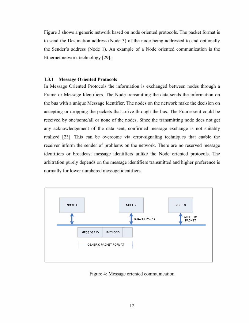
1.3.1 Message Oriented Protocols In Message Oriented Protocols the information is exchanged between nodes through a
Frame or Message Identifiers. The Node transmitting the data sends the information on
the bus with a unique Message Identifier. The nodes on the network make the decision on
accepting or dropping the packets that arrive through the bus. The Frame sent could be
received by one/some/all or none of the nodes. Since the transmitting node does not get
any acknowledgement of the data sent, confirmed message exchange is not suitably
realized [23]. This can be overcome via error-signaling techniques that enable the
receiver inform the sender of problems on the network. There are no reserved message
identifiers or broadcast message identifiers unlike the Node oriented protocols. The
arbitration purely depends on the message identifiers transmitted and higher preference is
normally for lower numbered message identifiers.
Figure 4: Message oriented communication
12
Figure 4 shows the communication between nodes in a message oriented methodology.
The packet that is sent on the network contains only the Message Identifier and not the
destination node’s address as in Node oriented mechanism. For example: in Figure 4
Node 2 rejects the packet and Node 3 accepts the packet. Example of a message oriented
network is Controller Area Network [6].
1.4 Medium Access Control (MAC) Medium Access Control (MAC) is the mechanism of establishing asynchronous
communication between nodes and this section briefs in detail on the strategies used on
the embedded networks in general. MAC determines which transmitter gets control over
the media for transmission. The MAC logic arbitrates between 2 or more nodes from
transmitting at the same time and prevents collision of information from different nodes.
MAC decisively controls the Real-time behavior and packet latency and choice of MAC
is essential in choosing the data communication protocol.
MAC can be generally classified into two categories as methods with deterministic access
and methods with random bus access. Deterministic bus access methods are in turn
classified into two methods as allowing centrally controlled arbitration and distributed
controlled arbitration. The non-deterministic or random bus access is classified into two
methods as methods allowing collisions and no collisions methodology.
In deterministic bus access method, the arbitration is clearly broken prior to a bus access
thus guaranteeing that only one node will get the bus for transmission. The maximum
system response time can be determined for the bus with accuracy. In centrally controlled
deterministic access, one or more nodes act as the master and determine which node gets
the bus. But if the master/s fails, then network communication is impossible. In
distributed controlled deterministic access, the arbitration is broken by individual nodes
based on a protocol and not controlled by a master node. Hence even if one or more
nodes fail in the network, communication is still possible between the remaining nodes.
Distributed controlled arbitration is more robust in fault-tolerant applications, but its
implementation is more complex than the centrally controlled arbitration.
13
In random bus access, any node on the network could send information once the bus is
idle. Since many different nodes can sense that the bus is idle at the same time, it is
referred to as Carrier Sense Multiple Access (CSMA). The random bus access can be
implemented with Collisions or without collisions. The random bus access without
collisions differs from collision-free bus access (as in deterministic bus access
implementation). The CSMA method in which collisions can occur but also can be
detected is called Carrier Sense Multiple Access/ Collision Detection (CSMA/CD). The
CSMA method in which collisions can occur but are identified later as error in
communication is implemented in the Local Operating Network protocol (LON) [23].
CSMA in which there are no collisions are called Carrier Sense Multiple Access/
Collision Avoidance (CSMA/CA).
1.5 Ardea Run-time Environment This section provides an overview on the Automatically Reconfigurable Distributed
Embedded Architectures (ARDEA) framework and the basic concepts of dependability
and fault-tolerance. Any safety-critical system that is being developed is a multitude of
hardware and software and the ability of the system to provide reliable functional service
as per its design is a principal paradigm in dependable computing.
In order to achieve high reliability on the data obtained, the system must be able to
withstand the errors that are generated in the system (either deliberate or due to design
flaws) or in case of failures, degrade gracefully or provide reduced services [25]. Hence a
fundamental requirement for any dependable system is to be fault-tolerant and to achieve
fault tolerance within the system redundant processing structures will have to be
incorporated in the system design phase [25].
ARDEA framework considers reconfiguration of the system as a mechanism of providing
fault-tolerance. Ardea framework supports traditional fault-tolerant techniques using
redundant modules and also graceful degradation [26]. The graceful degradation implies
that the system will reconfigure dynamically to produce reduced services of operation
14
depending on the type of fault suffered by the system and as the reconfiguration schemes
are supported in addition to the traditional fault tolerant schemes, make the Ardea
framework highly efficient in handling faults on the system. The dynamic reconfiguration
allows fault-tolerant applications to identify alternate modes of operation and not suffer
system failure during a catastrophic error, but rather have reduced services for the system
through reconfiguration.
The Ardea framework allows for reconfiguration of the architecture by capturing the
system architecture as Dependency Graphs (DG) and the DG’s indicate flow of data
between the modules within the Ardea framework. Redundant modules are also
incorporated into the DGs and the decision of correct data can be made by the process of
voting between the redundant modules. The voting process is represented using Logic-
gates on the DG and hence a DG can be used to represent redundant modules, logic gates,
input and output sources and the quality of the input or output sources. The flow of
information on a DG starts from the input sources end and terminates at the output
devices section. Figure 5 shows a model Ardea DG that shows functional flow of
information from the input modules to the output modules.
15
Figure 5: Ardea Dependency Graph model [26]
1.5.1 IDEAnix Framework IDEAnix task messaging framework [4] is critical for implementation for the Ardea
model where location independence of tasks is required for establishing seamless task
movement in the event of reconfiguration. The Ardea software framework consists of a
Real-Time Operating System (RTOS), application level software and a network interface
task. The application level software together with the RTOS and network interface task
were combined together to produce the IDEAnix framework where the tasks can be
moved seamlessly between the processor modules for reconfiguration of architecture as
required by the Ardea framework. The IDEAnix framework is a unique port of a MicroC
OS-II (uCOS-II) a real-time operating system for Si-Labs C8051F04x processors and
Keil compilers. IDEAnix framework includes boot-up and initialization routines specific
to the Si-Labs C8051F04x processors.
The framework consists of two layers of software:
1. Message Routing layer (MeRL)
2. A lower-level embedded network (CAN).
16
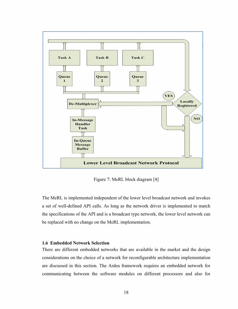
The MeRL exists on top of the uCOS-II operating system and uses the OS resources like
Queues, message boxes and multi-threading ability of the OS to control the data and
message flow between the different tasks. The MeRL abstracts the inter-task/ inter-
processor communication and the tasks can communicate seamlessly between tasks
running on same processor or to a task on a different processor without any change in the
running code. Figure 6 shows the IDEAnix block diagram with the task level
communication with the MeRL [4].
BROADCAST NETWORK DRIVER (CAN)
MeRL
USER TASKS
Figure 6: IDEAnix Block diagram and Task level communication with MeRL [4]
All the tasks running on the IDEAnix register for a message identifier with the MeRL and
the producer of the message broadcasts the packet with message identifier and data
through the network. The tasks running on the same processor or running on remote
processors receive the same packet information through the receiver buffer/queue and
will process the data through the FIFO buffer. This enables the task running on
independent processors be able to receive the same data as the tasks on the same
The following steps have to be repeated to clear all 32 the message objects CAN0ADR = 0x0F (IF1 – Data Register)
54
CAN0DATH = 0x00 (clearing bytes 2-3 of data reg)
CAN0DATL = 0x00 (Clearing bytes 0-1 of data reg)
Address is auto-incremented to CAN Data Register B1 and B2 CAN0DATH = 0x00 (clearing bytes 6-7 of data reg)
CAN0DATL = 0x00 (Clearing bytes 4-5 of data reg)
CAN0ADR = 0x08 (IF1 – Command Request)
CAN0DATL = 0x01 (Message Object Number)
Once the Command Request value is written with the Message object number, the
CANDAT register values are automatically transferred to the message objects in Message
RAM. CAN interrupts have to be enabled on the C805104x core to check for the
interrupts coming from C_CAN processor.
EIE2 = 0x20 (Enable CAN related interrupt)
SFRPAGE = 0x1 (CAN PAGE)
CAN0CN = 0x41 (Enable the CCE and init bit)
CAN0ADR = 0x03 (point to Bit timing register)
CAN0DAT = 0x6FC0 (Configuring Bit timing register)
0x6FC0 configures the bit-timing register for a bandwidth of 1Mbits/Sec. Finally the
CCE and Init bits are cleared and global interrupts are enabled to activate the CAN
engine. CAN0CN = 0x06 (Enable global interrupts)
CAN0CN = ~0x41 (Clear the CCE and init bit)
Two arrays of length 32, global to the entire driver module, are allocated to store the
message ids and the data corresponding to the message objects. The object array
(ObjArray) is of type integer and stores the message id received from the message object.
The data array (DataArray) is of type unsigned long and stores the data present in the
message objects. These arrays are used as software buffers to store the values before
sending the information to the higher layers.
55
4.2.2 Register Module This module is responsible for enabling a node to receive packets that are sent on the
network and in the C8051F04x board, it is possible for configuring a node to receive
either a packet with one specific message identifier or a range of message identifier. This
section explains the details on configuration (with corresponding Pseudo code) for
receiving a single packet or a range of packets and some fault tolerant techniques that can
be used to make the software more tolerant to faults due to message objects being full.
The CAN message handler in the C_CAN processor is responsible for receiving the
packets that are transmitted on the network and storing them in the Message RAM. It also
controls the Tx/Rx shift register in the C_CAN processor. Though all the packets that are
transmitted can be received by all the nodes on the network, the packets have to pass the
message filtering mechanism before they can be stored on the message objects.
The register module is responsible for configuring a message object to store packets with
one or a range of message ids. The CAN2.0A implementation can have 2048 (2^11)
different message ids and CAN2.0B can have 536,870,912 (2^29) different message ids.
But the maximum message objects available on the hardware are only 32 and hence some
message objects may have to be configured to receive more than one packet and the
arbitration masks are used for this purpose of specifying a range or multiple message ids
to occupy one message object.
Figure 15 shows the configuration steps that are involved in registering a node
with the given message identifier.
4.2.2.1 API Prototype exposed UINT8 reg_pkt ( CAN_ID_TYPE can_id);
56
Figure 15: Flow chart for Register module
57
4.2.2.2 Configuration of a message object for a single message id This section describes the steps (with corresponding Pseudo code) that are involved in
configuring a message object to receive a single message identifier. Before a message
object can be configured for the given message id, the initialization module checks to see
if any of the message object is available for configuration. If all the message objects are
full then an error CAN_MSGOBJS_FULL (201) is returned to the caller.
The message id (can_id) which is input through the API is checked against the values are
stored in ObjArray to see if the message id has already been registered for a message
object. If this condition is true, then an error CAN_DUPLICATE_ID_REG (204) is
returned to the caller indicating that an attempt has been made to register an id which has
already been configured.
A design decision is made on using Interface register 1 for configuring a message object
in receive mode and Interface register 2 for configuring a message object in transmit
mode, to enable the receive and transmit process to interrupt each other when required.
Interface register 1 is used for registering a message id with a message object as below: SFRPAGE = CAN0PAGE
CAN0ADR = 0x09 (IF1 Command Mask)
CAN0DAT = 0x00B8 (Set for write and use arbitration and
Control bits)
CAN0ADR = 0x0C (IF1 ARB1)
CAN0DAT= 0x00 (Set the higher 15 bits to zero)
Auto-incremented to IF1 ARB2 register and the Message valid bit is set to 1 and message
id is left shifted by 2 bits to copy the message id into bits 28-18. CAN0DAT = (0x8000) | (message_id << 2)
CAN0ADR = 0x0E (IF1 Message Control)
CAN0DAT = 0x0480 (Enable Rx Interrupt and do not use
Mask registers)
58
The message id is written into the command request register to enable transfer of data
from the IF1 registers to the Message objects. Finally the ObjArray is updated with the
message id for the corresponding message object.
CAN0ADR = 0x08 (IF1 Command Request)
CAN0DATL = (Message object number)
4.2.2.3 Configuration of a message object for group of message ids This section describes the configuration steps (with corresponding Pseudo code) that are
involved in configuring a message object to receive a single message identifier. The
initial checks are performed to identify, if a message id has already been configured or
check if the message objects are full, else corresponding error codes are returned to the
caller.
To register a message object with a group or range of message objects, the configuration
steps are followed as below: SFRPAGE = CAN0PAGE
CAN0ADR = 0x09 (IF1 Command Mask)
CAN0DAT = 0x00F8 (Set for write and use arbitration,
Mask and Control bits)
CAN0ADR = 0x0C (IF1 ARB1)
CAN0DAT= 0x00 (Set the higher 15 bits to zero)
CAN0DAT = 0x8000 (Set the Message valid bit)
The IF1 Mask register has to be used in this case to configure a group of message objects CAN0ADR = 0x0A (IF1 Mask Register)
CAN0DAT = 0x0000 (allows all the packets to be received
by the message object after acceptance filtering)
CAN0DAT = 0x0010 (allows packets with message ids from
0x10 – 0x1F to pass through the acceptance filtering
mechanism)
CAN0ADR = 0x0E (IF1 Message Control)
59
CAN0DAT = 0x1480 (Enable Rx Interrupt and use Mask
registers)
The message id is written into the command request register to enable transfer of data
from the IF1 registers to the Message objects. CAN0ADR = 0x08 (IF1 Command Request)
CAN0DATL = (Message object number)
4.2.2.4 Fault Tolerance mechanisms for Register module This section details some of the changes that might have to be added to include the fault
tolerant mechanisms. For implementation of a fault tolerant version of the software, the
register module is modified accordingly to meet the requirements.
The register module in the base version can register for only a maximum of 32 message
identifiers and any attempt to register for more message identifiers return an error to the
caller. This might lead to faults on a node requiring more than 32 packets with different
message identifiers.
Hence in order to accommodate for more message identifiers in the register module, a
group of message objects are allocated for normal configuration and another group of
message objects for special configurations. If the number of message objects under
normal configuration is filled, any message object allocated for special configuration is
chosen for receiving the packets with the given message identifier. The message object is
configured to receive all the packets and the given message identifier is stored
corresponding to the message object number. Subsequent calls to register unique
message identifiers are queued in the list for the message object.
Upon acceptance filtering, a packet with a message identifier that didn’t match normally
configured message objects, the packet is stored on the specially configured message
object. The message identifier value is checked against the values on the message id array
and if a match is found, the packet is forwarded to next layer, else it is discarded. This
60
mechanism ensures that only the packets that have been registered are fetched from the
message object and the rest of the packets are discarded.
4.2.3 Unregister Module This section explains some steps in configuring a message object that will prevent a node
from receiving the packet with the specific message identifier and also on some steps that
will make the unregister module more fault tolerant in case of using more than 32
message identifiers for a node.
The CAN application can dynamically unregister the message identifiers which have
been previously registered through the register modules and the unregister module
provides the capability to the software application to disassociate a node with a message
identifier at run-time.
After the message identifier has been successfully unregistered, the driver will not be
receiving packets with that specific message identifier or groups of message identifiers.
The same configuration steps are followed for unregistering a single message identifier or
groups of message identifiers. Figure 16 shows the steps that are involved in
unregistering a message identifier from a message object.
4.2.3.1 API Prototype exposed UINT8 unreg_pkt ( CAN_ID_TYPE can_id);
61
Figure 16: Flow chart for Unregister module
4.2.3.2 Steps to unregister a message identifier: This section describes the steps (with corresponding Pseudo code) that are involved in
unregistering a message object to receive a single message identifier. The message
identifier that is input is checked against the ObjArray to check if the message identifier
has been registered previously for a message object. The unregister module returns an
error message of CAN_UNREG_ID_ERR (205) if the message identifier is already not
registered with the driver.
62
The message object configured to receive the message identifier is obtained by searching
through the ObjArray and then arbitration register is cleared to remove the association of
the message id with the object. The message id entry in the ObjArray is cleared to
remove all associations of the identifier with the message object.
SFRPAGE = 0x1 (CAN PAGE SFR)
CAN0ADR = 0x09 (IF1 command Mask Register)
CAN0DAT = 0x00B8 (Set the Write)
CAN0ADR = 0x0C (IF1 Arbitration register 1)
CAN0DAT = 0x0000 (clear the upper 15 bits of msg id)
CAN0DAT = 0x0000 (clear the lower 15 bits of msg id)
CAN0DAT = 0x0000 (Message control reg. is cleared)
CAN0ADR = 0x08 (IF1 Command Request register)
CAN0DAT = message object number
4.2.3.3 Fault tolerant mechanism for Unregister module: This section details some of the changes that might have to be added to include the fault
tolerant mechanisms. For implementation of a fault tolerant version of the software, the
unregister module is modified accordingly to meet the requirements.
The unregister module checks to see if the message identifiers that are configured are less
than the maximum allowed for normal configuration, if true, then the module simply
unregisters the message identifier and returns to the caller. If the message identifiers that
are configured are more or equal to the maximum number of message objects available
(MAX_MSG_OBJS_RX in our current implementation) then the message identifier is
unregistered from the message object and a message identifier from the special
configuration list is fetched and stored in the message object for reception. If the
message object with special configuration has no message identifiers to receive, then the
message object is unregistered from receiving any packets.
63
This mechanism will ensure that when the message objects equal the number of message
identifiers required, only normal configurations will remain and all the special
configurations will be unregistered.
4.2.4 Get Packet Module This section explains how the Get packet module returns the packet data information to
the calling application. When the message identifiers have been registered with the driver
and the packets that match the acceptance filtering are stored in the corresponding
message objects.
As a part of the design, the first N number of message objects (user defined at compile
time) are configured for receiving data and the last 32-(N+R) ( N is the number of
message objects reserved for receiving packets and R is the number of other reserved
message objects by translation module) message objects are configured for transmitting
data. Once the data has been fetched from the message object, the data bytes from the
message object will be cleared and hence are stored in software buffers (ObjArray and
DataArray) in the Driver layer until they are either fetched by the calling application or
overwritten by new data.
The Get packet module searches through the ObjArray to check for the matching
message identifier stored in any of the message objects. If any match was found, the
corresponding data from the DataArray is returned to the calling application and if a
match was not found among the message objects, a payload data of 0 and message
identifier of 0 (which is illegal on the CAN network) is sent back to the calling
application to indicate that there was no packets for the message identifier requested.
4.2.4.1 API Prototype exposed UINT8 get_pkt ( CAN_ID_TYPE *can_id_ptr,
PAYLOAD_TYPE *payload_ptr);
64
4.2.4.2 Fault Tolerant implementation for Get packet module This section gives an overview of the some of the modifications that have to be made to
the Get Packet module to make it fault tolerant. The existing implementation of the get
packet module is a non-blocking call and fetches the data bytes from the ObjArray and
DataArray. It is entirely possible that the message object could have been updated with a
new value by the time this packet is being read from the Software buffers.
The fault tolerant implementation would have to make the get_pkt call a blocking
synchronous call with the function checking a global packet receipt variable flag to see if
packet data has ever been overwritten in the message object before the get_pkt call. This
flag has to be set in the Interrupt service routine when it is invoked due to packet lost
error. If the global packet receipt flag was set for the message identifier, this implies that
some packet was lost due to overwrite and has to be informed to the caller with an
appropriate error code and return the latest packet message that was received.
This mechanism will ensure that both the data lost due to overwrites and the latest packet
that was successfully received on the network is captured and the caller of the API is
informed of the loss of packets.
4.2.5 Send Packet Module The Send Packet module is responsible for sending the packet data through the CAN bus
and this section explains the basic configurations involved in configuring a node to send
CAN2.0A and CAN2.0B packets on the network. The maximum payload that can be sent
through the CAN bus is 8 bytes, but after examining the maximum packet size for the
application, the maximum payload size for a packet through the CAN bus for the
CANOED UAV was restricted to 4 bytes.
This restriction is application specific and can be readily modified by changing the
compile time Macros. Figure 17 shows the steps involved in configuring a message
object to be able to transmit a packet on the network.
65
4.2.5.1 API Prototype exposed
UINT8 send_pkt (CAN_ID_TYPE can_id,
PAYLOAD_TYPE payload);
UINT8 send_pkt_ext (CAN_ID_TYPE can_id,
PAYLOAD_TYPE payload);
CALLED BY APPLICATION
SET THE IF2 COMMAND MASK REG TO WRITE
WRITE ARBITRATION BITS INTO IF2 ARB1 & ARB2 REGS
SET THE MSG VALID BIT AND THE PAYLOAD LENGTH
WRITE INTO THE IF2 COMMAND REQ REG WITH
MSG OBJ NUMBER
EXIT
IF CAN2.0A TYPE?
SET MESSAGE ID TO 11 BITS
SET MESSAGE ID TO 29 BITS
YES NO
Figure 17: Flow chart for Send Message Module
4.2.5.2 Configuration steps to send 11-bit (CAN 2.0A) packet on the network This section describes the steps that are to be followed to configure a message object for
transmitting a CAN2.0A type of packet and this configuration has to be every time a
66
packet is sent out as the message identifier for sending could be different. The number of
message objects to be configured as transmit only are user-dependant (defined at compile
time).
The last 32-(N+R) message objects are configured for transmit purposes and to enable
faster transmission of data sent by the application and the send packet module goes
through these message objects in Round-Robin to choose the next message object to
configure for sending. For the purposes of interacting with the message objects, Interface
register 2 is used to keep the Transmit & Receive pipelines isolated and also to provide
them with the ability to interrupt each other to send or receive higher priority messages.
The Configuration steps for the message objects are shown below: SFRPAGE = 0x1 (CAN PAGE)
CAN0ADR = 0x21 (IF2 Command Mask)
CAN0DAT = 0x0087 (Set the Write bit, alter all
except Mask bits)
CAN0ADR = 0x24 (IF2 Arbitration register 1)
CAN0DAT = 0x00 (Set upper 15 bits to zero in
CAN2.0A implementation)
Setting Message Valid bit and loading the message id in bits 18-28 bits of ARB2 register CAN0DAT = 0xA000 | (message id <<2)
CAN0DAT = 0x8000 | (MAX_PAYLOAD_LENGTH)
Setting the transmit request bit and data length code and copying data bytes into IF2 data
register CAN0ADR = 0x27 (IF2 Data register 1)
CAN0DATH = Data byte [1]
CAN0DATL = Data byte [0]
CAN0DATH = Data byte [3]
CAN0DATL = Data byte [2]
67
Finally the IF2 Command Request register is written with the message object to start the
transfer of data from the Registers to the Message RAM. CAN0ADR = 0x20
CAN0DATL = (message object number)
4.2.5.3 Configuration steps to send 29-bit packet on the network This section describes the steps involved in sending a CAN2.0B type packet and a user-
dependent number of message objects are chosen for configuration of CAN2.0B type
packets. Some message objects may be configured for translation purposes and to enable
faster transmission of data sent by the application and the send packet extended frame
module goes through these message objects in Round-Robin to choose the next message
object to configure for sending.
For the purposes of interacting with the message objects, Interface register 2 is used to
keep the Transmit & Receive pipelines isolated and also to provide them with the ability
to interrupt each other to send or receive higher priority messages.
The Configuration steps for the message objects are shown below: SFRPAGE = 0x1 (CAN PAGE)
CAN0ADR = 0x21 (IF2 Command Mask)
CAN0DAT = 0x0087 (Set the Write bit, alter all
except Mask bits)
CAN0ADR = 0x24 (IF2 Arbitration register 1)
CAN0DAT = 0x0000|(message id) (Filling 0-15 bits with
the message id)
Setting Message Valid bit and loading the message id in bits 18-28 bits of ARB2 register CAN0DAT = 0xB000 | (0x00)( Setting Extended bit)
Message Control Register setting TX request bit and maximum payload CAN0DAT = 0x8000 | (MAX_PAYLOAD_LENGTH)
68
Setting the transmit request bit and data length code and copying data bytes into IF2 data
register CAN0ADR = 0x27 (IF2 Data register 1)
CAN0DATH = Data byte [1]
CAN0DATL = Data byte [0]
CAN0DATH = Data byte [3]
CAN0DATL = Data byte [2]
Finally the IF2 Command Request register is written with the message object to start the
transfer of data from the Registers to the Message RAM. CAN0ADR = 0x20
CAN0DATL = (message object number)
4.2.5.4 Fault Tolerant implementation for Send packet module
The send packet module in the present implementation is an asynchronous call (non-
blocking) and the module returns to the caller after configuring the message object for
transmit. There is a possibility that packets ready for transmit could be lost by
overwriting if the send packet module is invoked faster than the time taken by the CAN
controller could send packets on the network. This scenario is possible when the Transmit
shift register on the CAN controller waits for the bus to be free while higher priority
packets are occupying the bus and the send packet module is invoked and it overwrites
the existing message identifier and payload with the new information.
As there is no hardware based logic to identify such a scenario of overwrite on the
transmit buffer, the send packet call will have to be synchronous and it could read a
global transmit flag for data and the flag could be updated by the Interrupt service routine
when a packet is sent. This mechanism ensures that there is a One to one correspondence
with the send_pkt call and packets sent on the network else a corresponding error is
returned to the caller and any failure to transmit a packet on the network can also be
tracked due to this implementation.
69
4.2.6 Translation Module (CAN2.0A CAN2.0B CAN2.0A) The translation module implementation details are discussed in this section and it
converts the packets of CAN 2.0A format into CAN 2.0B format and vice versa in detail.
By hardware design, C_CAN processor is complaint with both CAN2.0A and CAN2.0B
standards. But the message objects as per rule cannot be configured to send or receive
both CAN2.0A and CAN2.0B packets and each message object can send or receive either
CAN2.0A or CAN2.0B type of packets. Due to this hardware limitation, the software has
to be written separately to translate the packets that are of type CAN2.0A to CAN2.0B
type and vice versa.
The translation module is responsible for receiving packets that have 11-bit or 29-bit
identifiers and converts the packets into the format required. There is no significant
change when an 11-bit identifier is converted into a 29-bit identifier with the other 18 bits
simply being padded as zeros. But when a 29-bit identifier is truncated into an 11-bit
identifier, care has to be taken to ensure that there are no conflicts with any other
message 11-bit identifier frame. In either case the payload should be kept unaffected and
transmitted as received. This has to be ensured during the system design phase and static
assignment of message identifiers to sub-systems eliminates possible clashes among
nodes during the translation.
The significance of the translation module in the CANOED UAV project is that the
Piccolo Auto-pilot generates packets in CAN2.0B format and all the other sub-systems
on the network receives / transmits packets in CAN2.0A format [21]. The driver
implements two API’s that can be invoked separately to translate data from one format
into another. Figure 18 illustrates the functionality of the translation module and
interaction of the software and registers on the CAN Controller.
4.2.6.1 API Prototype exposed UINT8 can11_to_29(CAN_ID_TYPE can_id);
UINT8 can29_to_11(CAN_ID_TYPE can_id);
70
MSG OBJ FOR 2.0AMSG OBJ FOR 2.0B
CAN BUS
SEND_PACKET SEND_PACKET_EXT
CAN2.0APACKET
CAN2.0B PACKET
IF REGISTERS
CAN ISR
CONVERSION FROM 2.0A FRAME TO
2.0B FRAME
CONVERSION FROM 2.0B FRAME TO
2.0A FRAME
IF CAN2.0A PACKET IS RXD
IF CAN2.0B PACKET IS RXD
Figure 18: Translation Module block Diagram
4.2.6.2 Steps in implementing the CAN 11-bit to CAN 29-bit translator This section describes the sequence to follow to convert a CAN 2.0A type packet into a
CAN 2.0B type packet. The message identifier that is input is checked to identify if it has
already been configured to be received by the register module by looking up the
ObjArray. If the message identifier was already registered with some other message
object, then the message object is disassociated with the message identifier. A message
identifier list is created so that the identifiers that have to be converted from CAN 2.0A to
CAN 2.0B are stored and compared with the packets received after the packets are
received in the message object. Configuring a message object for receiving all the packets
are described in register module section. After the configuration, the module returns to
the calling application with the appropriate error code or CAN_DRIVER_NOERROR if
no error was found.
71
4.2.6.3 Steps in implementing the CAN 29-bit to CAN 11-bit translator This section describes the sequence to follow to convert a CAN 2.0B type packet into a
CAN 2.0A type packet. A message identifier list is created to maintain the list of message
identifiers to be converted. The message object allocated for translation purposes is
configured for receiving a CAN 2.0B type packet as follows: SFRPAGE = CAN0PAGE
CAN0ADR = 0x09 (IF1 Command Mask)
CAN0DAT = 0x00F8 (Set for write and use Mask,
Arbitration and Control bits)
CAN0ADR = 0x0C (IF1 ARB1)
CAN0DAT= 0x00 (Set the higher 15 bits to zero)
CAN0DAT = 0x8000 (Set the Message valid bit to 1)
The IF1 Mask register is configured to receive all the packets of type CAN 2.0B and the
IF1 Message control registers are configured to receive interrupts on successful packet
reception. CAN0ADR = 0x0A (IF1 Mask Register)
CAN0DAT = 0x0000 (sets the higher 15 bits of mask to
zero)
CAN0DAT = 0x8000(allows all the CAN2.0B frames to be
received by the message object after acceptance
filtering)
CAN0ADR = 0x0E (IF1 Message Control)
CAN0DAT = 0x1480 (Enable Rx Interrupt and use Mask
registers)
The message id is written into the command request register to enable transfer of data
from the IF1 registers to the Message objects. After the configuration, the module returns
to the calling application with CAN_DRIVER_NOERROR (1) if no error or the
Finally the Global Interrupt is enabled to restore the normal execution of the processor.
4.2.7.2 Fault tolerant implementations of the CAN ISR This section describes possible extensions to the CAN ISR implementation to make the
software architecture fault tolerant. As per the present implementations, the CAN ISR has
been configured to act only upon successful reception of packets and this feature could be
extended to include successful transmission of packets or to identify errors on the
network.
If the successful transmit interrupt is enabled, then the CAN ISR will set a global variable
flag that will be monitored by the Send Packet or Send Packet Extended modules to
confirm the transfer of a packet on the line. This mechanism can be used to maintain a
one-to-one correspondence to the function call and the packet transfer on the network.
77
78
Similarly if error interrupts are enabled, then the Last changed Error codes (LEC) values
are read and then can be used to identify the problems on the network. The Error codes
will enable a node to enter the “Error Passive” or “Error Active” or “Bus Off” modes and
this would be used in fault detection and isolation mechanism implementations for the
node.
Finally the present CAN ISR implementation does not include the functionality of the
CAN Translator module and when added into the CAN ISR has to be modified from its
standard operation. If the interrupt has been generated by the RxOK and the message
object with the new data has been configured to translate CAN2.0A to CAN2.0B, then
the Arbitration data and packet payload is read from the message object. The Arbitration
id is padded up to 29-bits and the send_packet_ext() API is invoked with the message id
and payload.
If the interrupt has been generated by RxOK and the message object with the new data
has been configured to translate CAN2.0B to CAN2.0A, then arbitration data and
payload is read from the message object. The Arbitration id is truncated to 11-bit
identifier and send_packet() API is invoked with message id and payload.
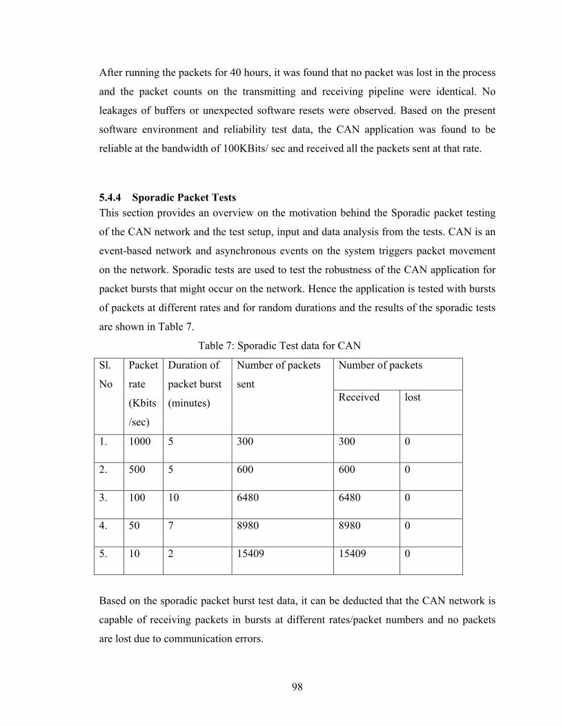
Chapter 5: CAN Performance & Reliability Tests
5.1 Background Chapter 1 discussed the details on implementing the ENDURA layer for a distributed
system and the fault tolerant schemes to be add within the driver for safety critical
applications. For a reconfigurable architecture based system, the reliability and
performance of the system has to be analyzed thoroughly before it can be deployed in
applications.
This chapter has been dedicated to describe the test setup on which the tests were run, the
Conformance requirements and tests, observations and performance analysis tests, data
and report. The performance analysis tests include bandwidth testing, Inter-layer Latency
tests, reliability tests and sporadic packet testing. The Conformance tests includes
verification of the services offered by the CAN layer and adherence to the protocol. The
ENDURA layer is tested as a stand-alone module and also integrated into the MeRL,
IDEAnix layers.
5.2 Test bench Set-up The details on setting up the test bench for Conformance and performance tests are
discussed in this section. The test set-up includes at least 2 Si-Labs C8051F040
evaluation boards connected through a custom-made CAN bus, a PCAN CAN packet
analyzer, a JTAG debugger to burn the user code onto the flash of C8051F040 boards and
RS232 cables to monitor the debugging output from the processors. Figure 20 explains
the connectivity between the nodes and mechanisms to send inputs/ view outputs. Figure
21 and Figure 22 provide a snap shot view on the actual set-up that is used for testing and
also the connections on the set-up.
79
Figure 20: Block diagram for ENDURA test set up
Figure 21: Test Bench Setup for ENDURA layer testing
80
Figure 22: Test bench set up (a closer look)
5.2.1 Steps to set up the test-bench The procedure in setting up the test bench to analyze the ENDURA implementation and
application is overviewed in this section. The test bench includes 2 or more Si-Labs
C8051040 boards, a PCAN sniffer and a custom-made CAN bus. To configure the test
bench, the CAN bus is connected to the CAN ports of the C8051F040 boards and the
PCAN Sniffer is connected and launched on a desktop computer. For debugging
purposes, RS-232 serial cables are connected to the appropriate ports of C8051F040
boards and optionally they may be connected to a desktop computer to analyze the debug
outputs.
The ENDURA software is compiled together with the IDEAnix framework and MicroC
OS-II using the Keil cross compiler for the Si-Labs C8051F040 board and on successful
compilation, the executable is downloaded onto the C8051F040 boards through Si-Labs
IDE software and JTAG in-circuit emulator. The code is executed on the processors by
starting the application through the Si-Labs IDE software. The debug console on the
81
desktop computer (using HyperTerminal) is monitored and the software can be tested by
providing appropriate input on the debug console.
5.3 CAN 2.0A/ B conformance testing This section provides an overview on the conformance test requirements, the test inputs
and the observations of the tests. The ENDURA implementation has to meet the basic
functional requirements of the CAN 2.0A and CAN 2.0B protocol in order to be
compatible with other implementations of CAN. This is a critical requirement for
integrating with other devices that are CAN compatible. For example in the UAV project
the COTS Auto-pilot used sends packets in CAN 2.0B type formats and these packets
should be received without errors by the CAN application. Before testing for
conformance, the test bench is set up as indicated in Section 5.2.1 to feed input and to
analyze the results.
The conformance test for the ENDURA layer includes the following:
1. Registering an identifier
2. Unregister an identifier
3. Send a packet with any identifier
4. Receive a packet (for identifiers registered)
5.3.1 Register identifier test The test logic and inputs used in testing the Register module are discussed in this section.
This test checks for the conformance of the register packet module by inputting different
message identifiers and monitoring whether the ENDURA layer can accept those packets.
Some invalid message identifiers are also input to test the functionality of the driver.
Once the software is initialized, a packet with message identifier 0x5 and arbitrary
payload of 4 bytes is sent through the CAN bus (from PCAN sniffer). The get_pkt() API
is invoked (by pressing one of the options on the debug screen) and the resulting value
82
from the API is checked. As the message identifier 0x5 is not registered with the system,
the message id and payload should be equal to 0.
After this, the reg_pkt() API is invoked from the debug console (by pressing one of the
options on the debug screen) and the message identifier 0x5 is entered. A packet with
message id 0x5 and arbitrary payload of 4 bytes is sent from the PCAN sniffer software
and the get_pkt() API is invoked. The value of message identifier and payload returned
by the get_pkt() API is compared with the value sent and verified and the payload and the
message id should match.
The reg_pkt() API is invoked multiple times for same identifier and this should result in
an error code different from CAN_DRIVER_NOERROR. The test can be repeated to
check the boundary conditions by registering for more than 32 message identifiers.
5.3.1.1 Test Result 1. Register message is found to register the identifier as expected and the packets
with the registered message identifier are received correctly.
2. The Register message returned an error (CAN_DRIVER_ERROR) when an
invalid message identifier was entered.
3. The register message module returned an error (CAN_DUPLICATE_ID_REG)
when the message id has already been registered with other message object
4. The module returned an error (CAN_MSGOBJS_FULL) when an attempt was
made to register for more than 32 message identifiers.
5.3.1.2 Test Observation Based on the above test results, the register module is found to be working as per the
requirements for the CAN 2.0A/ B protocols.
5.3.2 Unregister a Message Identifier Test The test logic and inputs used in testing the Unregister module are discussed in this
section. This test checks for the conformance of the unregister packet module by
83
inputting different message identifiers and monitoring whether the ENDURA layer can
disassociate itself from receiving those packets. Some invalid message identifiers are also
input to test the functionality of the driver.
First a message identifier 0x5 is registered for the node by invoking reg_pkt() API and a
packet is sent through the PCAN sniffer with the message id 0x5. Then get_pkt() API is
invoked to check if the packet is received successfully by the driver. After verifying the
reg_pkt() functionality, the unreg_pkt() API is invoked with the message identifier 0x5
and the same packet with message identifier 0x5 and arbitrary payload is sent from the
PCAN sniffer. Finally get_pkt() API is invoked to verify if the packet is still being
received by the node or not. The unreg_pkt() API is also invoked multiple times with the
same message identifier and also with invalid identifiers to check for the correct
functionality of the unregister module.
5.3.2.1 Test Result 1. The unregister message module works as expected when a call is made to
unregister an already registered id, the module removes all association of the
message id from the message object and the node no longer receives the packet
from the bus.
2. The unregister module returns the error codes (CAN_UNREG_ID_ERR) to the
caller if any attempt is made to register an already unregistered message id.
3. The unregister module also returns an error code (CAN_UNREG_ID_ERR) when
given an invalid message identifier is input.
5.3.2.2 Test Observation Based on the test results, the unregister module is found to be working as per the
requirements for the CAN 2.0A/ B protocols.
84
5.3.3 Send Packet Test This test validates the conformance of the send packet module by inputting different
message identifiers and monitoring the CAN bus to verify if the packets have been
successfully been sent by the test node. This test can be performed in conjunction with
the Get Packet module test by receiving the packets sent from the test node. Some invalid
message identifiers are also input to test the functionality of the module driver.
send_pkt() API is invoked with the desired message identifier 0x5 and arbitrary payload
and the message identifier, data that is sent is verified using another node registered for
the particular message identifier or through the PCAN sniffer. Similar test is performed
using send_pkt_ext() API to test successful sending of an extended CAN frame and
monitored using PCAN sniffer. The send packet module is tested for boundary conditions
by entering a 0x7FF (2.0 type packet) message identifier and 0x1FFFF (extended CAN
type). These are the last valid message identifiers allowed by each of the protocols and
these packets should be successfully be sent on the network.
Send packet module is tested for invalid message identifiers by entering a message
identifier 0x0 and arbitrary payload. A message identifier of 0x00 is invalid in the CAN
protocol and should not be sent on the network.
5.3.3.1 Test Result 1. All valid packets with message identifiers 0x5, 0x7FF, 0x1FFFF are all seen on
the PCAN sniffer validating the sending of valid packets on the network.
2. The packets with message id 0x0 is not sent on the network and error code
(CAN_DRIVER_ERROR) is returned to the caller.
5.3.3.2 Test Observation Based on the above tests, the send module is found to be working as expected and meets
the conformance required for the CAN2.0 A/ B protocols.
85
5.3.4 Receive packet module test This test checks for the conformance of the receive packet module by verifying for
successful reception of packets that are sent from another node. This test can be
performed in conjunction with the Register packet module and Send Packet module
testing by receiving the packets sent from the Send Packet module.
First the reg_pkt() API is invoked with message identifier 0x05 to enable the node to
receive the packets of the message identifier from the network. From the other node, the
send_pkt() API is invoked with message identifier 0x5 and arbitrary payload or through
the transmit section of the PCAN sniffer. The get_pkt() API is invoked and checked for
the message identifier and payload sent through the PCAN sniffer or through any other
node. The get_pkt() API is invoked repeatedly to check for value returned by the module.
5.3.4.1 Test Result 1. The get_pkt() API returns the latest packet that was received by the node and the
payload and message identifier is found to match the values sent.
2. The get_pkt() API invoked without sending any packet returns 0x0 for the
message id and 0x0 for the payload for the packet.
5.3.4.2 Test Observation Based on the above tests, the receive packet module is found to be working as expected
and was able to receive the packets that were sent to the module. Please refer to the
Performance test section for the efficiency of the get_pkt() API implementation and the
limitations of the driver software.
5.4 Performance Testing of ENDURA The performance tests that are subject on the ENDURA layer, the test logic behind the
inputs, the results and the observations made after analysis of output data are discussed in
this section. The Conformance test for CAN only provides the accuracy of the
implementation with respect to the CAN protocols and it does not indicate any reliability
86
or performance information. For this purposes, rigorous performance and reliability tests
were performed on the ENDURA layer to observe the performance data for the driver.
ENDURA implementation is tested with a series of performance tests for analysis of the
ability of the driver to perform at various loads. The performance tests can be broadly
classified into 3 sections:
1. Bandwidth Tests and analysis
2. Packet Latency tests
3. Endurance testing
5.4.1 Bandwidth Tests and Analysis The main objective of the ENDURA layer is to enable communication between nodes
with maximum speed/efficiency possible and hence bandwidth data provided by the
ENDURA implementation is critical to understand the effectiveness of the network driver
and suitability of the network for the application. The requirements for the bandwidth
tests, the different test logics applied on the CAN application, analysis of the results with
the expected value and feasibility study of application are explained in this section. For
testing the bandwidth provided by CAN application, the build of IDEAnix integrated
with the ENDURA layer is considered together with MicroC OS-II.
An application is developed as a user thread on top of the IDEAnix with priority 5 and
another thread with priority 4 (higher priority user thread) is assigned to the network
router that is responsible for routing incoming packets to the corresponding tasks. The
application thread registers for a message identifier through the reg_pkt() API and a
packet with that particular message identifier is sent through the PCAN Sniffer or
through a separate node that has an application thread sending packets continuously.
It is observed that as the packet transmit pipeline takes longer time than the packet
receive pipeline and hence a delay has to be inserted into the send_pkt() and get_pkt()
module to synchronize the sender and receiver with uniform time interval. Any
implementation of the packet receive and transmit pipeline without the software delay
87
swamped the limited number of software buffers available for the driver/ IDEAnix layers
and resulted in packets being lost due to overwriting of software buffers. The bandwidth
is measured under different OS delay values entered on the Receive Packet routine
against the rate at which the packet is sent to the nodes and the results are discussed in the
Sections 5.4.1.1 and Sections 5.4.1.2, which describe the bandwidth test scenarios with 2
different delay timings at the receive packet pipeline of the CAN application.
5.4.1.1 Bandwidth Analysis for 100ms delay in packet receive pipeline This section provides an analysis on the data obtained from the bandwidth tests of
ENDURA by substituting a delay of 10 OS ticks (100ms) between the every successive
packet transmit/receive call and Table 3 shows the relevant data for the different rates of
packet transmission. It is observed that with bit-rate of approximately 1 to 2 Kbits/Sec
(100ms between successive packets) packets are lost at the receiving end. This is
expected because the application thread has to enable context switching for the network
router thread to process the next packet in queue and as the OS delay is at 10 OS ticks
(100ms), any data that is sent at rate faster than the OS delay will be lost due to overhead
of context switching. Hence the OS delay values are reduced and further analyzed in
section 5.4.1.2.
Table 3: Bandwidth Analysis report for 100ms tick delay
Bit Rate
(Bits/sec)
Number of packets
sent
Number of
packets Rxd
Number of packets
Lost
108 5000 5000 0
216 5000 5000 0
432 5000 5000 0
1K 5000 5000 0
2K 5000 3948 1052
10K 5000 2894 2106
20K 5000 1634 3366
100K 5000 945 4055
88
5.4.1.2 Bandwidth Analysis for 10ms delay in packet receive pipeline An analysis on the data obtained from the bandwidth analysis of ENDURA layer by
substituting a delay of 1 OS tick (10ms) is explained in this section. The data in Table 4
indicates that with a 10ms delay between successive packets, the CAN application starts
to lose packets at 20K bits/sec. This is expected as the inter-packet delay is decreased by
a factor of 10, the bandwidth is increased by a factor of approximately 10 as well, as the
10ms delay between packets, drops packet at approximately 20K Bits/sec It is observed
that with rate approximately equaling 100K, packets are lost at the receiver due to
overwriting of packet data. The minimum inter-packet time delay that can be achieved for
the ENDURA implementation with IDEAnix and MicroC OS-II is 10ms and with this
minimum inter-packet time delay, it is possible to receive all the packets on the network
with no packet being lost.
Table 4: Bandwidth Analysis report for 10ms tick delay
Bit Rate
(Bits/sec)
Number of packets
sent
Number of
packets received
Number of packets
lost
108 5000 5000 0
216 5000 5000 0
432 5000 5000 0
1K 5000 5000 0
2K 5000 5000 0
10K 5000 5000 0
20K 5000 5000 0
100K 5000 1783 3217
89
Bandwidth Analysis: Packets dropped
0
500
1000
1500
2000
2500
3000
3500
4000
4500
108 216 432 1K 2K 10K 20K 100K
Bit Rate (Bits/Sec)
Num
ber o
f Pac
kets
Delay of 100ms Delay of 10ms
Figure 23: Bandwidth Graph for Packet rate Vs Packets dropped
5.4.1.3 Bandwidth Analysis with Packets sent over time The Bandwidth Analysis with respect to the time taken to send packets between node is
discussed in this section. The projection on bandwidth is made by sending a fixed number
of packets and measuring the time taken to receive the packets successfully to calculate
the bandwidth on the network. Table 5 shows the relevant data for the number of packets
sent against time taken to send them and bandwidth data for the entire network is
calculated based on the data from the table.
Table 5: Bandwidth Analysis with number of packets sent over time
Number of
packets sent
Number of packets Time taken to send packets (sec)
Received lost
65531 65531 0 75
90
Number of Packets transmitted = 65531
Number of bits per packet = 108 (approximately)
Time taken to send = 75 seconds
Total number of bits sent = No. of Packets transmitted * No. of bits/packet
Competition Design”, University of Kentucky, Lexington, KY 40506, Spring 2006.
[5] CAN in Automation. Am Weichselgarten 26, DE-91058 Erlangen, http://www. can-
cia.org, September 7, 2007.
[6] CAN Specification version 2.0, Part A. Robert Bosch GmbH, Stuttgart, Germany,
1991.
[7] CAN Specification version 2.0, Part B, Robert Bosch GmbH, Stuttgart, Germany, 1991. [8] KVaser Incorporated. 567 W Channel Island Blvd #336, Port Hueneme, CA 93041,
http://www.kvaser.com, September 7, 2007.
[9] K. H. Johansson, M. Torngren, L. Nielsen, “Vehicle Applications of
Controller Area Network”, Handbook of Networked and Embedded Control Systems,
Birkhäuser, 2005. Invited paper.
[10] Light Electric Vehicle Conference Presentation, Hsinchu Taiwan, March 2007.