1
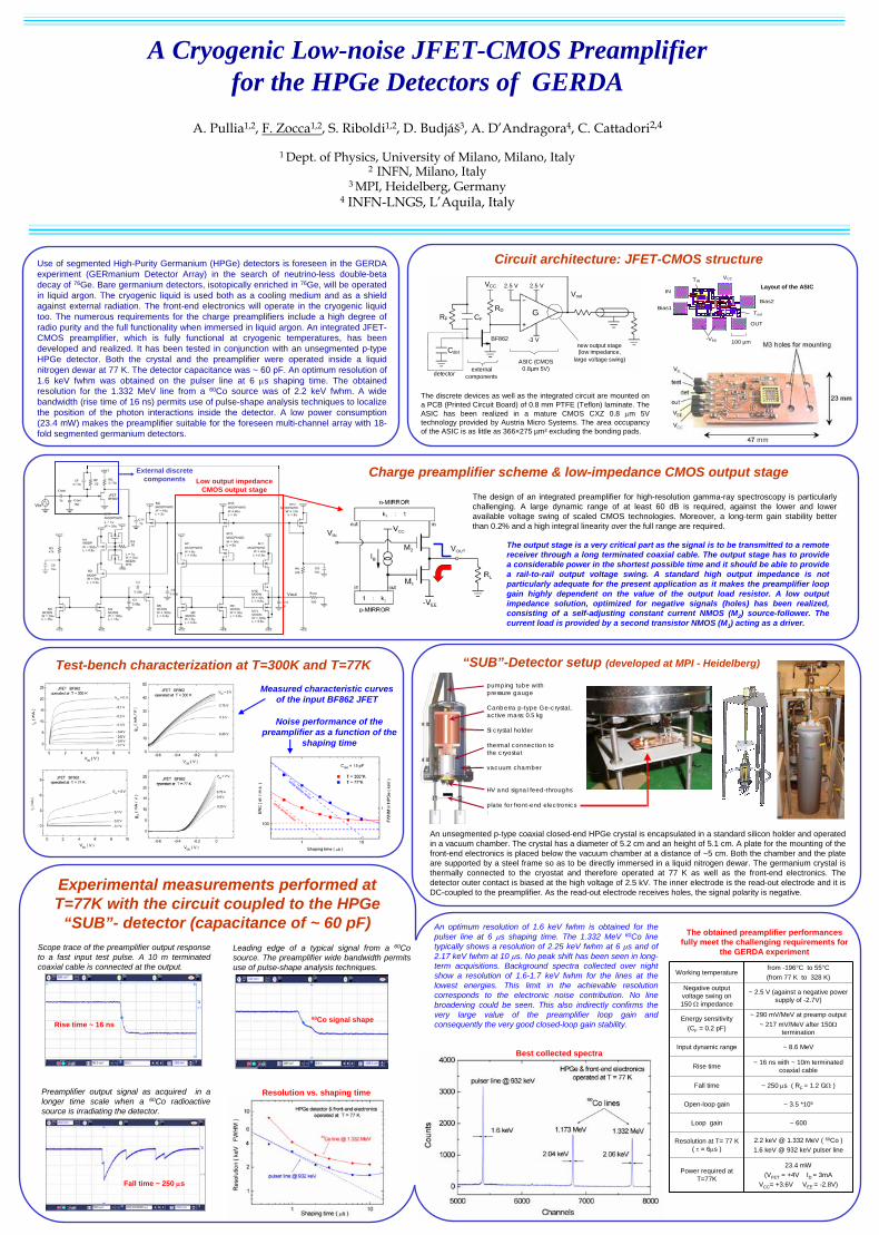
A Cryogenic Low-noise JFET-CMOS Preamplifier for the HPGe Detectors of GERDA A. Pullia 1,2 , F. Zocca 1,2 , S. Riboldi 1,2 , D. Budjáš 3 , A. D’Andragora 4 , C. Cattadori 2,4 1 Dept. of Physics, University of Milano, Milano, Italy 2 INFN, Milano, Italy 3 MPI, Heidelberg, Germany 4 INFN-LNGS, L’Aquila, Italy Circuit architecture: JFET-CMOS structure Use of segmented High-Purity Germanium (HPGe) detectors is foreseen in the GERDA experiment (GERmanium Detector Array) in the search of neutrino-less double-beta decay of 76 Ge. Bare germanium detectors, isotopically enriched in 76 Ge, will be operated in liquid argon. The cryogenic liquid is used both as a cooling medium and as a shield against external radiation. The front-end electronics will operate in the cryogenic liquid too. The numerous requirements for the charge preamplifiers include a high degree of radio purity and the full functionality when immersed in liquid argon. An integrated JFET- CMOS preamplifier, which is fully functional at cryogenic temperatures, has been developed and realized. It has been tested in conjunction with an unsegmented p-type HPGe detector. Both the crystal and the preamplifier were operated inside a liquid nitrogen dewar at 77 K. The detector capacitance was ~ 60 pF. An optimum resolution of 1.6 keV fwhm was obtained on the pulser line at 6 µs shaping time. The obtained resolution for the 1.332 MeV line from a 60 Co source was of 2.2 keV fwhm. A wide bandwidth (rise time of 16 ns) permits use of pulse-shape analysis techniques to localize the position of the photon interactions inside the detector. A low power consumption (23.4 mW) makes the preamplifier suitable for the foreseen multi-channel array with 18- fold segmented germanium detectors. RD CF BF862 Cdet detector Vout G new output stage (low impedance, large voltage swing) RF 2.5 V -3 V external components ASIC (CMOS 0.8μm 5V) VCC 2.5 V External discrete components Low output impedance CMOS output stage 100 μm VCC OUT IN -VEE Bias2 Bias1 TIN Tout The output stage is a very critical part as the signal is to be transmitted to a remote receiver through a long terminated coaxial cable. The output stage has to provide a considerable power in the shortest possible time and it should be able to provide a rail-to-rail output voltage swing. A standard high output impedance is not particularly adequate for the present application as it makes the preamplifier loop gain highly dependent on the value of the output load resistor. A low output impedance solution, optimized for negative signals (holes) has been realized, consisting of a self-adjusting constant current NMOS (M 2 ) source-follower. The current load is provided by a second transistor NMOS (M 1 ) acting as a driver. Charge preamplifier scheme & low-impedance CMOS output stage Measured characteristic curves of the input BF862 JFET Experimental measurements performed at T=77K with the circuit coupled to the HPGe “SUB”- detector (capacitance of ~ 60 pF) The discrete devices as well as the integrated circuit are mounted on a PCB (Printed Circuit Board) of 0.8 mm PTFE (Teflon) laminate. The ASIC has been realized in a mature CMOS CXZ 0.8 µm 5V technology provided by Austria Micro Systems. The area occupancy of the ASIC is as little as 366×275 μm² excluding the bonding pads. The design of an integrated preamplifier for high-resolution gamma-ray spectroscopy is particularly challenging. A large dynamic range of at least 60 dB is required, against the lower and lower available voltage swing of scaled CMOS technologies. Moreover, a long-term gain stability better than 0.2% and a high integral linearity over the full range are required. Working temperature from -196°C to 55°C (from 77 K to 328 K) Negative output voltage swing on 150 Ω impedance ~ 2.5 V (against a negative power supply of -2.7V) Fall time ~ 250 µs ( R F = 1.2 GΩ ) Open-loop gain ~ 3.5 *10 5 Energy sensitivity (C F = 0.2 pF) ~ 290 mV/MeV at preamp output ~ 217 mV/MeV after 150Ω termination Input dynamic range ~ 8.6 MeV Rise time ~ 16 ns with ~ 10m terminated coaxial cable Loop gain ~ 600 Resolution at T= 77 K ( τ = 6µs ) 2.2 keV @ 1.332 MeV ( 60 Co ) 1.6 keV @ 932 keV pulser line Power required at T=77K 23.4 mW (V FET = +4V I D = 3mA V CC = +3.6V V EE = -2.8V) pumping tube with pressure gauge Canberra p-type Ge-crystal, active mass: 0.5 kg Si crystal holder thermal connection to the cryostat vacuum chamber HV and signal feed-throughs plate for front-end electronics Noise performance of the preamplifier as a function of the shaping time Test-bench characterization at T=300K and T=77K “SUB”-Detector setup (developed at MPI - Heidelberg) An unsegmented p-type coaxial closed-end HPGe crystal is encapsulated in a standard silicon holder and operated in a vacuum chamber. The crystal has a diameter of 5.2 cm and an height of 5.1 cm. A plate for the mounting of the front-end electronics is placed below the vacuum chamber at a distance of ~5 cm. Both the chamber and the plate are supported by a steel frame so as to be directly immersed in a liquid nitrogen dewar. The germanium crystal is thermally connected to the cryostat and therefore operated at 77 K as well as the front-end electronics. The detector outer contact is biased at the high voltage of 2.5 kV. The inner electrode is the read-out electrode and it is DC-coupled to the preamplifier. As the read-out electrode receives holes, the signal polarity is negative. Scope trace of the preamplifier output response to a fast input test pulse. A 10 m terminated coaxial cable is connected at the output. Rise time ~ 16 ns Fall time ~ 250 µs 60 Co signal shape Preamplifier output signal as acquired in a longer time scale when a 60 Co radioactive source is irradiating the detector. Leading edge of a typical signal from a 60 Co source. The preamplifier wide bandwidth permits use of pulse-shape analysis techniques. An optimum resolution of 1.6 keV fwhm is obtained for the pulser line at 6 µs shaping time. The 1.332 MeV 60 Co line typically shows a resolution of 2.25 keV fwhm at 6 µs and of 2.17 keV fwhm at 10 µs. No peak shift has been seen in long- term acquisitions. Background spectra collected over night show a resolution of 1.6-1.7 keV fwhm for the lines at the lowest energies. This limit in the achievable resolution corresponds to the electronic noise contribution. No line broadening could be seen. This also indirectly confirms the very large value of the preamplifier loop gain and consequently the very good closed-loop gain stability. Best collected spectra The obtained preamplifier performances fully meet the challenging requirements for the GERDA experiment Layout of the ASIC Resolution vs. shaping time


![C22 Preamplifier Complete User Manual - Analog Metricanalogmetric.com/download/C22 Preamplifier Complete User Manual.pdf · [C22 VACUUM TUBE PREAMPLIFIER COMPLETE USER MANUAL ] ...](https://static.documents.pub/doc/80x56/5ad3f8607f8b9abd6c8eae98/c22-preamplifier-complete-user-manual-analog-preamplifier-complete-user-manualpdfc22.jpg)


