A Disruptive Approach to Electric Vehicle Power Electronics R. Erickson (PI), D. Maksimovic, K. Afridi 2015 Annual Merit Review June 9, 2015 DOE Vehicle Technologies Program This presentation does not contain any proprietary, confidential, or otherwise restricted information Department of Electrical, Computer, and Energy Engineering University of Colorado, Boulder FOA: Vehicle Technologies Incubator Area: Power Electronics—Topologies Project ID: EDT072
Transcript
A Disruptive Approach toElectric Vehicle Power Electronics
R. Erickson (PI), D. Maksimovic, K. Afridi
2015 Annual Merit ReviewJune 9, 2015
DOE Vehicle Technologies Program
This presentation does not contain any proprietary, confidential, or otherwise restricted information
Department of Electrical, Computer, and Energy EngineeringUniversity of Colorado, Boulder
FOA: Vehicle Technologies IncubatorArea: Power Electronics—TopologiesProject ID: EDT072
Overview
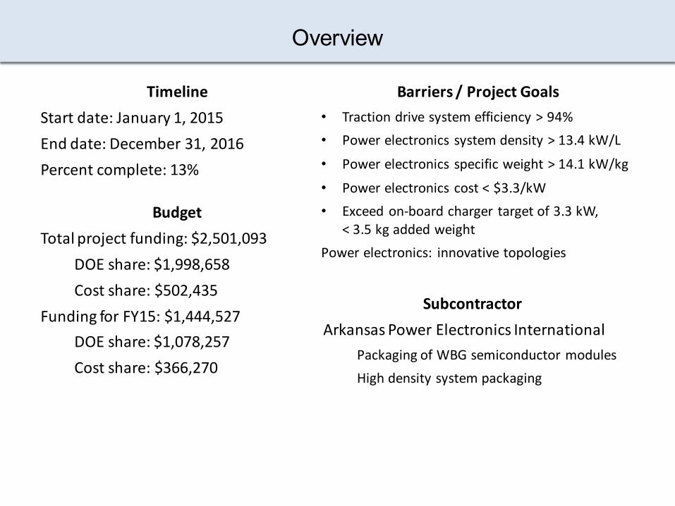
TimelineStart date: January 1, 2015End date: December 31, 2016Percent complete: 13%
Barriers / Project Goals • Traction drive system efficiency > 94%• Power electronics system density > 13.4 kW/L
• Power electronics specific weight > 14.1 kW/kg
• Power electronics cost < $3.3/kW• Exceed on-board charger target of 3.3 kW,
< 3.5 kg added weightPower electronics: innovative topologies
BudgetTotal project funding: $2,501,093
DOE share: $1,998,658Cost share: $502,435
Funding for FY15: $1,444,527DOE share: $1,078,257Cost share: $366,270
SubcontractorArkansas Power Electronics International
Packaging of WBG semiconductor modulesHigh density system packaging
Relevance
Project addresses APEEM R&D goals: Innovative power electronics topologies that improve traction drive system size, cost, weight, and efficiency
APEEM 2020 Goal Goals of this Project
Traction drive system (power electronics plus motors):
Efficiency > 94%
• Power electronics US06 average efficiency improved from 92.5% to 97.5%: 30 kW drivetrain architecture demonstration
Power electronics density> 13.4 kW/L
• WBG high density demonstration: > 13.4 kW/L
Power electronics specific weight> 14.1 kW/kg
• WBG high density demonstration: > 14.1 kW/kg
Power electronics cost< $3.3/kW
• Reduced film capacitor requirements:Capacitor specific energy reduced from 9 J/kW to < 5 J/kW
• Reduced cooling system requirements:Pout/Ploss improved from 10 to over 30
These goals will be achieved through a new Composite Converter technology that achieves significant and non-incremental performance gains
DOE PHEV Charger 2022 targets Projections for this Project
30 kW drivetrain architecture demonstration WBG high density packaging demonstration
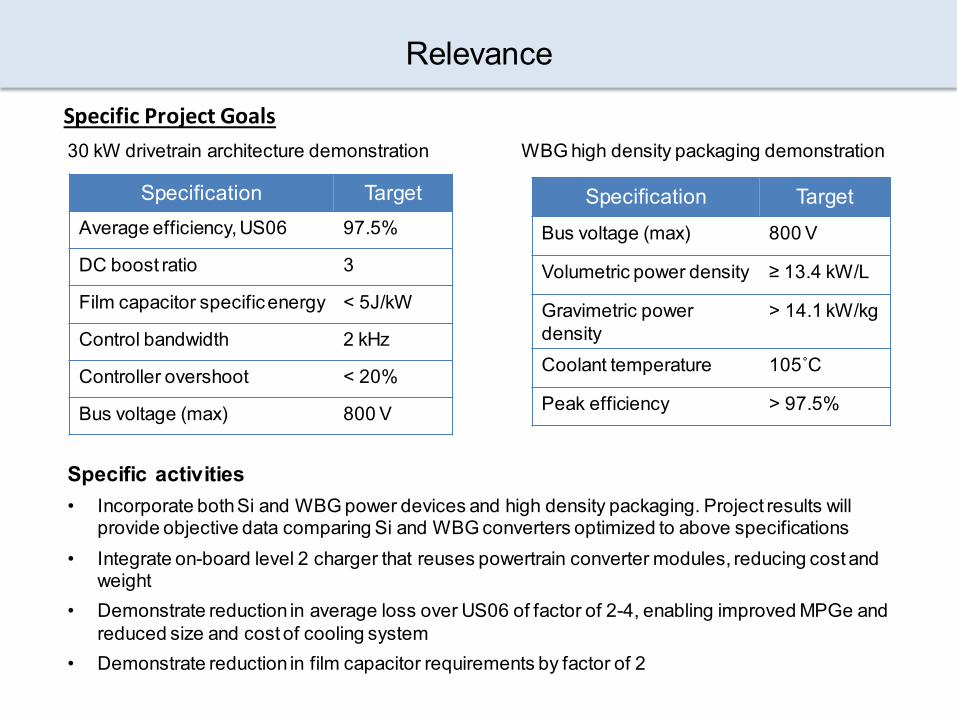
Specific activities• Incorporate both Si and WBG power devices and high density packaging. Project results will
provide objective data comparing Si and WBG converters optimized to above specifications• Integrate on-board level 2 charger that reuses powertrain converter modules, reducing cost and
weight• Demonstrate reduction in average loss over US06 of factor of 2-4, enabling improved MPGe and
reduced size and cost of cooling system• Demonstrate reduction in film capacitor requirements by factor of 2
Specific Project Goals
2015 Milestones
Date Milestones and Go/No-Go Decisions Status
March 2015Milestone:Architecture definition complete
Complete
June 2015Milestone:Module designs complete
On track
October 2015Milestone:Module construction complete
• Efficiency ≥ 98.5% at Vbatt = 250 V, Vbus = 650 V, P = 15 kW• Efficiency ≥ 96.5% at Vbatt = 250 V, Vbus = 650 V, P = 30 kW
Approach / Strategy
Demonstrate new composite converter topology that leads to fundamental performance improvements including average efficiency, film capacitor size, and on-board charger size.
CompositeDC-DC
ConverterInverter
MotorVbusVbatt
+
-
+
-
Integrated Charger
3φ-AC
Technology Switching frequency
US06 average efficiency
Relative FilmCapacitor Vrated Irms
Conventional, Si IGBT 10 kHz 92.5% 1.0
Conventional, WBG (GaN or SiC) 100 kHz 94% 1.0
Proposed composite, Si MOSFET 30 kHz 97.5% 0.3
Proposed composite, WBG 100 kHz 97.5% 0.3
Composite converter technology improves average efficiency and film capacitor size. Increase of switching frequency improves magnetics size.
Approach / Strategy
!"#$%&'(
!"#$%)*
+,
-"#$%)*
!"!#$.(/*012!
12%
12&
12'
13!
13%
13&
13'
Fig. 3. Power stage of the DC Transformer (DCX) module
9LQ
9RXW
'&�7UDQVIRUPHU�'&;�
1'&;
%XFN
0EXFN�
��
� %RRVW
0ERRVW
Fig. 4. Proposed modular converter system level architecture
L
C1 C2Q1/D1
Q2/D2
Fig. 5. Circuit diagram of power stage of the boost and buck modules
benefit of adding the buck module is that the output voltagestress can be evenly shared between DCX and boost modulesthrough variation of the buck conversion ratio, and thereforethe transistor voltage stresses can be controlled to be half of themaximum output voltage. If we denote the conversion ratios ofthe buck and boost modules as Mbuck and Mboost respectively,then the system conversion ratio is M = MbuckNDCX + Mboost.
It is not necessary to switch all three modules at the sametime. The buck and boost modules have highest efficiency inthe pass-through mode (Mbuck = 1 or Mboost = 1), whereac losses are zero and only conduction loss remains. Thisspecific operating mode is illustrated as in Figure 6; onlythe DCX operates (with optimized soft switching) and hencesystem efficiency is very high at this point. With pulse-widthmodulation of a buck or boost module at a duty cycle Dnear the pass-through value, the adjacent operating regions areexpected to achieve high efficiency as well. For example, it ispossible to operate the boost module in the pass-through modewhen M < 1+NDCX , and the buck module in the pass-throughmode when M > 1+NDCX . Furthermore, if the output voltage is
9LQ
9RXW� �9LQ������1'&;�
'&�7UDQVIRUPHU�'&;�
1'&;
%XFN0EXFN� ��
%RRVW
'� ����SDVV�WKURXJK
0ERRVW� ��
'� ����SDVV�WKURXJK
�
�
�
�9LQ
�
�
9LQ1'&;�
�
�
�9LQ
Fig. 6. Modular converter operation with both buck and boost module atpass-through
lower than the boost module voltage rating, it is also possibleto shut down both the buck and the DCX modules, and operatethe boost module alone. Finally, if the input voltage is large,even when M > 1+NDCX , it may still be necessary to operatebuck module to limit the DCX output voltage within its voltagerating.
With this composite converter approach, both the powerrating and the voltage rating of each module is reduced.Therefore lower voltage devices, with reduced on-resistanceas well as faster switching speed, can be used. Reactors canalso be optimized with reduced power ratings and reducedapplied voltages. It is also possible to design and optimize eachmodule independently, according to their respective operatingranges. Although the system requires a larger number of powerelements such as transistors, capacitors, etc., the sizes of theseelements are reduced. The total power silicon area can becomparable to that of the conventional boost converter, buthigher average efficiency is achieved.
With this architecture the number of capacitors is increasedcompared to the conventional boost converter. However, thevoltage ratings and rms current ratings of the capacitors aresubstantially reduced, leading to a net reduction in capacitorsize and cost. With the use of lower voltage semiconductors,the switching frequency of each module can be increased,which will reduce the required capacitance and inductance aswell.
III. Design Optimization
In many applications, although the system is designedto be able to handle worst case operating conditions such
Conventional Boost: multiple Si IGBT die are connected in parallel in multichip power semiconductor module • 10 kHz switching frequency • Poor partial power efficiency • High rms current in DC bus
capacitors • Efficiency of boost converter
dominates system efficiency
Power [kW]0 5 10 15 20 25 30
Effic
ienc
y [%
]
90
92
94
96
98
100
Proposed composite converterConventional boost
Efficiency improvement in proposed composite architecture vs. conventional boost: Vbatt = 250 V, Vbus = 650 V
Proposed composite boost converter architecture Partial-power dc-dc converter modules • Silicon area is same as in conventional boost • Improved efficiency by reduction of switching loss and
magnetics ac loss, through use of passthrough modes and reduced module voltages
• Substantially reduced RMS capacitor currents Fundamental improvements in performance arising from new superior converter architecture
DC-DC Converter Inverter
Motor Vbus Vbatt
+
-
+
-
Integrated Charger
!""#$%&'(&'%'")*+,$+, -(./0#+%&'(0'%1)*+,$+,
2"$",
Conventional Proposed
Technical Accomplishments
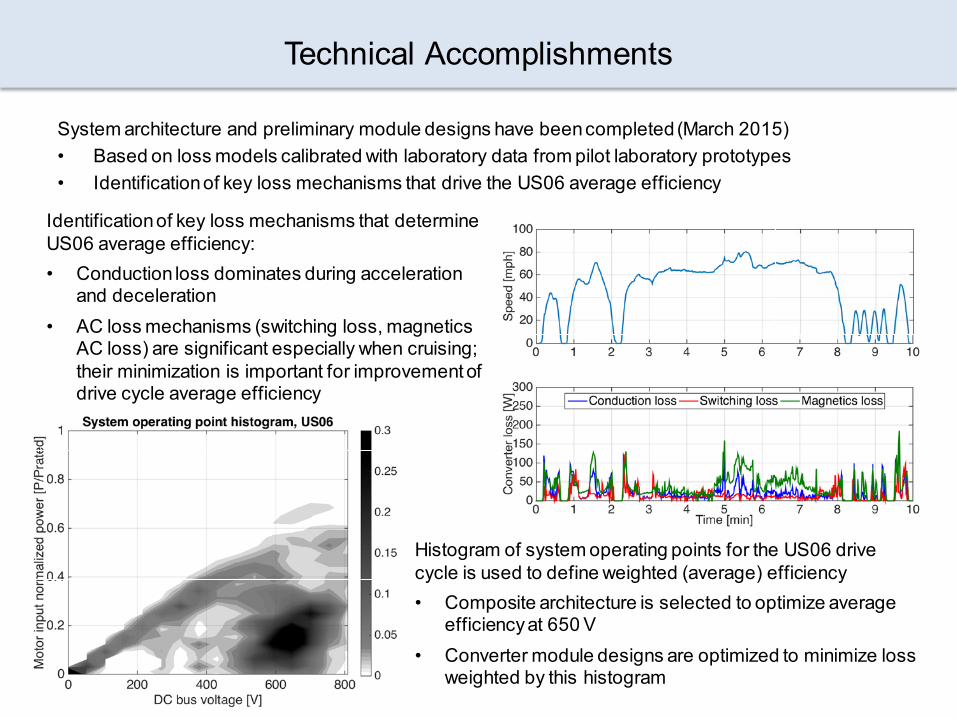
System architecture and preliminary module designs have been completed (March 2015)• Based on loss models calibrated with laboratory data from pilot laboratory prototypes• Identification of key loss mechanisms that drive the US06 average efficiency
Identification of key loss mechanisms that determine US06 average efficiency:• Conduction loss dominates during acceleration
and deceleration• AC loss mechanisms (switching loss, magnetics
AC loss) are significant especially when cruising; their minimization is important for improvement of drive cycle average efficiency
Histogram of system operating points for the US06 drive cycle is used to define weighted (average) efficiency• Composite architecture is selected to optimize average
efficiency at 650 V• Converter module designs are optimized to minimize loss
weighted by this histogram
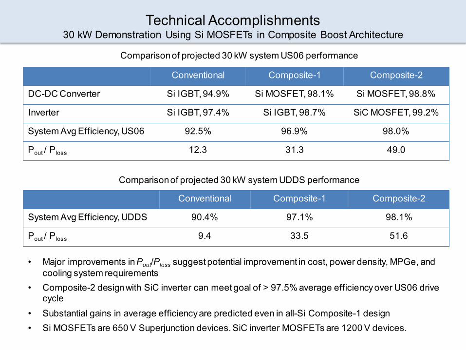
Technical Accomplishments30 kW Demonstration Using Si MOSFETs in Composite Boost Architecture
Comparison of projected 30 kW system US06 performance
Conventional Composite-1 Composite-2
DC-DC Converter Si IGBT, 94.9% Si MOSFET, 98.1% Si MOSFET, 98.8%
Inverter Si IGBT, 97.4% Si IGBT, 98.7% SiC MOSFET, 99.2%
System Avg Efficiency, US06 92.5% 96.9% 98.0%
Pout / Ploss 12.3 31.3 49.0
Comparison of projected 30 kW system UDDS performance
Conventional Composite-1 Composite-2
System Avg Efficiency, UDDS 90.4% 97.1% 98.1%
Pout / Ploss 9.4 33.5 51.6
• Major improvements in Pout/Ploss suggest potential improvement in cost, power density, MPGe, and cooling system requirements
• Composite-2 design with SiC inverter can meet goal of > 97.5% average efficiency over US06 drive cycle
• Substantial gains in average efficiency are predicted even in all-Si Composite-1 design • Si MOSFETs are 650 V Superjunction devices. SiC inverter MOSFETs are 1200 V devices.
Technical AccomplishmentsImprovement of Cruising (Light Load) Efficiency
Comparison of efficiency curves at Vbatt = 250 V, Vbus = 650 V
Composite-1 Composite-2
Original composite converter
95.9% 96.8%
Extended ZVS 96.9% 98.0%
Composite-1 Composite-2
Original composite converter
96.9% 97.8%
Extended ZVS 97.1% 98.1%
Reduction of switching loss at low current, to improve system average efficiency
Effect on US06 average efficiency Effect on UDDS average efficiency
• Switching loss behaves roughly as a fixed loss that dominates efficiency at low power
• Zero-voltage switching (ZVS) can be introduced into Buck and Boost modules at low current, through selection of inductor values, to reduce switching loss
• In Q1, we developed a new approach to extend DCX zero-voltage switching to low current. This leads to a substantial improvement in cruising efficiency and average drive cycle efficiency (blue efficiency curve).
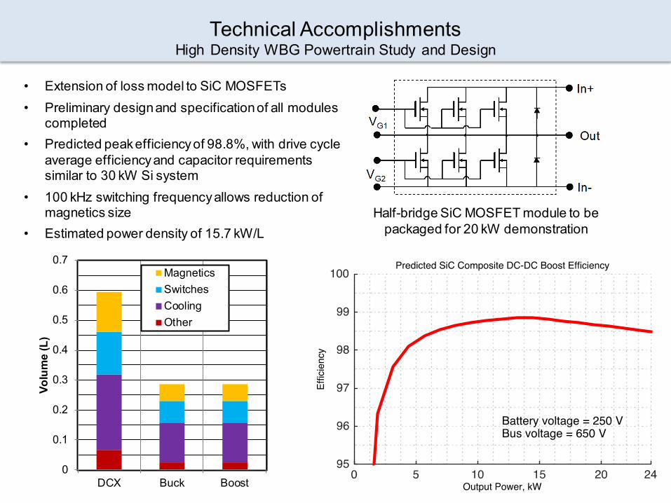
Technical AccomplishmentsHigh Density WBG Powertrain Study and Design
0
0.1
0.2
0.3
0.4
0.5
0.6
0.7
DCX Buck Boost
Volu
me
(L)
MagneticsSwitchesCoolingOther
Half-bridge SiC MOSFET module to be packaged for 20 kW demonstration
• Extension of loss model to SiC MOSFETs• Preliminary design and specification of all modules
completed• Predicted peak efficiency of 98.8%, with drive cycle
average efficiency and capacitor requirements similar to 30 kW Si system
• 100 kHz switching frequency allows reduction of magnetics size
• Estimated power density of 15.7 kW/L
0 5000 10000 150000
50
100
150
200
250 total
switching
magnetics
switching - secondary
switching - primary
magnetics – TX wire
magnetics - Ldcx
magnetics – TX core
DCX Output Power
DC
X Lo
sses
(W
)
Pout = 10kW, ηDCX=98.6%
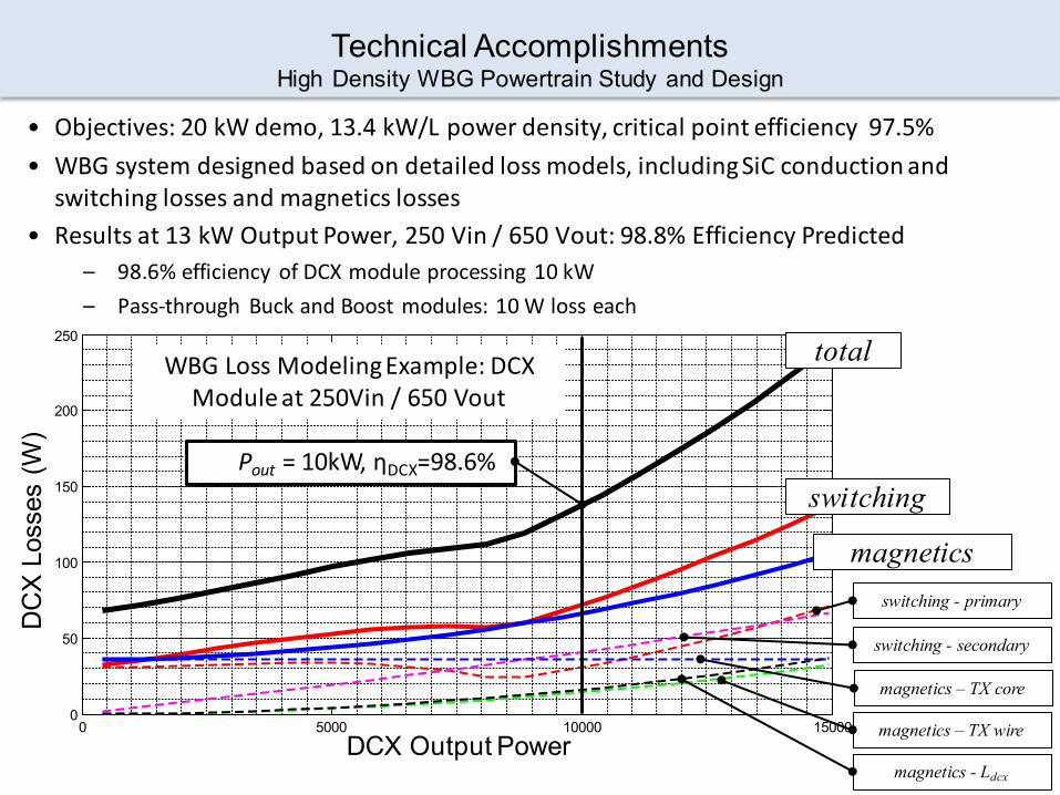
• Objectives: 20 kW demo, 13.4 kW/L power density, critical point efficiency 97.5%• WBG system designed based on detailed loss models, including SiC conduction and
switching losses and magnetics losses• Results at 13 kW Output Power, 250 Vin / 650 Vout: 98.8% Efficiency Predicted
– 98.6% efficiency of DCX module processing 10 kW– Pass-through Buck and Boost modules: 10 W loss each
Technical AccomplishmentsHigh Density WBG Powertrain Study and Design
WBG Loss Modeling Example: DCX Module at 250Vin / 650 Vout
Technical AccomplishmentsIntegrated Charger System
• Four architectures were considered and compared. The above architecture has been selected as the most promising.
• Charger reuses composite converter modules• Preliminary design of level 2 charger is complete• Projected efficiency of added modules: 97.7%• Design result for integrated 6.6 kW level 2 charger: added mass 1.6 kg, added specific weight
4 kW/kg exceeds DOE PHEV 2022 targets of 3.3 kW, 3.5 kg, 1 kW/kg• Demonstration of Si MOSFET prototype this year, and SiC prototype in year 2
Selected system architecture: charger integration within the composite DC=DC converter
Responses to Previous Year Reviewers’ Comments
• This project is a new start
Partnerships and Collaborations
• Arkansas Power Electronics International—subcontractorSupplying packaged WBG power semiconductor modulesSystem-level high-density packaging
• General Electric CoSupplying SiC MOSFET devices
• InfineonSupplying GaN devices
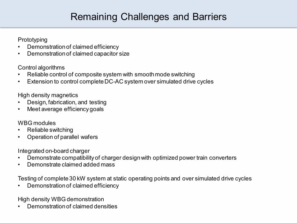
Remaining Challenges and Barriers
Prototyping• Demonstration of claimed efficiency• Demonstration of claimed capacitor size
Control algorithms• Reliable control of composite system with smooth mode switching• Extension to control complete DC-AC system over simulated drive cycles
High density magnetics • Design, fabrication, and testing• Meet average efficiency goals
WBG modules• Reliable switching• Operation of parallel wafers
Integrated on-board charger• Demonstrate compatibility of charger design with optimized power train converters• Demonstrate claimed added mass
Testing of complete 30 kW system at static operating points and over simulated drive cycles• Demonstration of claimed efficiency
High density WBG demonstration• Demonstration of claimed densities
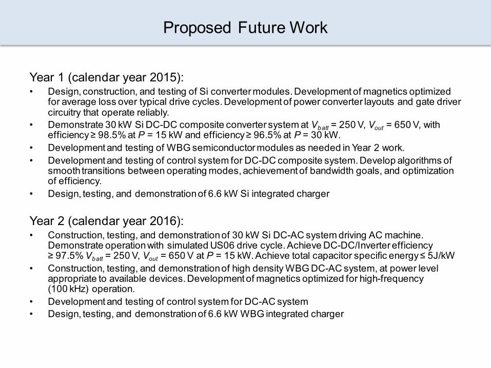
Proposed Future Work
Year 1 (calendar year 2015):• Design, construction, and testing of Si converter modules. Development of magnetics optimized
for average loss over typical drive cycles. Development of power converter layouts and gate driver circuitry that operate reliably.
• Demonstrate 30 kW Si DC-DC composite converter system at Vbatt = 250 V, Vout = 650 V, with efficiency ≥ 98.5% at P = 15 kW and efficiency ≥ 96.5% at P = 30 kW.
• Development and testing of WBG semiconductor modules as needed in Year 2 work.• Development and testing of control system for DC-DC composite system. Develop algorithms of
smooth transitions between operating modes, achievement of bandwidth goals, and optimization of efficiency.
• Design, testing, and demonstration of 6.6 kW Si integrated charger
Year 2 (calendar year 2016):• Construction, testing, and demonstration of 30 kW Si DC-AC system driving AC machine.
Demonstrate operation with simulated US06 drive cycle. Achieve DC-DC/Inverter efficiency ≥ 97.5% Vbatt = 250 V, Vout = 650 V at P = 15 kW. Achieve total capacitor specific energy ≤ 5J/kW
• Construction, testing, and demonstration of high density WBG DC-AC system, at power level appropriate to available devices. Development of magnetics optimized for high-frequency (100 kHz) operation.
• Development and testing of control system for DC-AC system• Design, testing, and demonstration of 6.6 kW WBG integrated charger
Summary
Conventional Project target Projected result
US06 avg effcy 92.5% 97.5% 98.0%
Cap spec energy 9J/kW ≤ 5J/kW 4J/kW
Project target Projected result
US06 avg effcy 97.5% 98.0%
Power density ≥ 13.4 kW/L 15.7 kW/L
Specific weight ≥ 14.1 kW/kg 14.1 kW/kg
Summary of design and projected performance, Si 30 kW demonstration
Summary of design and projected performance, WBG high-density demonstration
Q1 work is complete: tradeoff study of approaches to meet efficiency, density, and cost-related goals has led to selected designs for both a Si 30 kW demonstration and a WBG high-density demonstration that are projected to meet or exceed these goals.
Technical Back-Up Slides
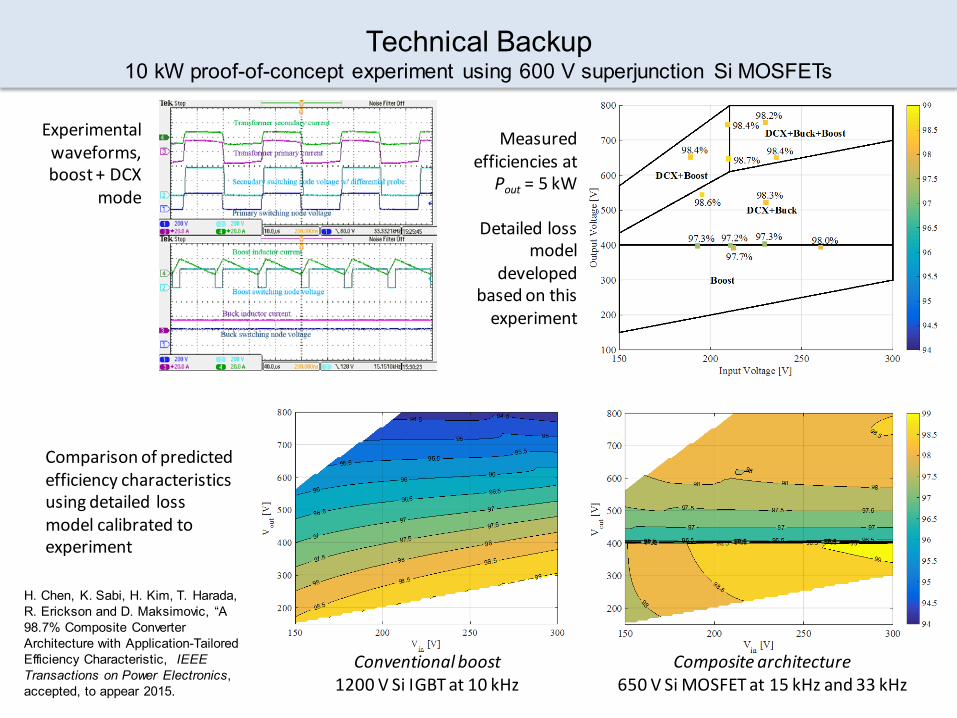
Technical Backup10 kW proof-of-concept experiment using 600 V superjunction Si MOSFETs
Experimental waveforms, boost + DCX
mode
Measured efficiencies at
Pout = 5 kW
Detailed loss model
developed based on this
experiment
Conventional boost1200 V Si IGBT at 10 kHz
Composite architecture650 V Si MOSFET at 15 kHz and 33 kHz
Comparison of predicted efficiency characteristics using detailed loss model calibrated to experiment
H. Chen, K. Sabi, H. Kim, T. Harada, R. Erickson and D. Maksimovic, “A 98.7% Composite Converter Architecture with Application-Tailored Efficiency Characteristic, IEEE Transactions on Power Electronics, accepted, to appear 2015.
Technical Backup Extension of DCX Zero-Voltage Switching Region to Low Power Operating Points
13 13.5 14 14.5Tank
indu
ctor
cur
rent
[A]
-40-20
0204060
Time [7s]13 13.5 14 14.5H
-brid
ge v
olta
ge [V
]
-200
0
200
vpvs'
At heavy load, tank inductor has enough energy to achieve primary side full ZVS
13 13.5 14 14.5Tank
indu
ctor
cur
rent
[A]
-40
-20
0
Time [7s]13 13.5 14 14.5H
-brid
ge v
olta
ge [V
]
-200
0
200
vpvs'
At light load, tank inductor does not have enough energy to achieve primary side full ZVS. Active switching causes switching loss
Use of magnetizing current to assist ZVS at low power, plus additional commutation (dead) time, extends ZVS range
Analysis shows that ZVS can be achieved at all power levels with sufficiently small magnetizing inductance and long enough commutation interval. Design equations were developed.
3/2015 result: with DCX operating at 11% of its rated power, a 70% reduction of loss is measured in laboratory pilot converter.
0 0.2 0.4 0.6 0.8 1 1.2 1.4
Vo
ltag
e [V
]
-200
0
200v
p
vs
Time [7s]0 0.2 0.4 0.6 0.8 1 1.2 1.4
Cu
rren
t [A
]
-5
0
5
10
15
il
im
Old control hard-switching point
Extending zero-voltage switching to low power via introduction of transformer gap and variable dead time. Top: simulations of transistor voltages and winding currents. Bottom: laboratory waveforms.
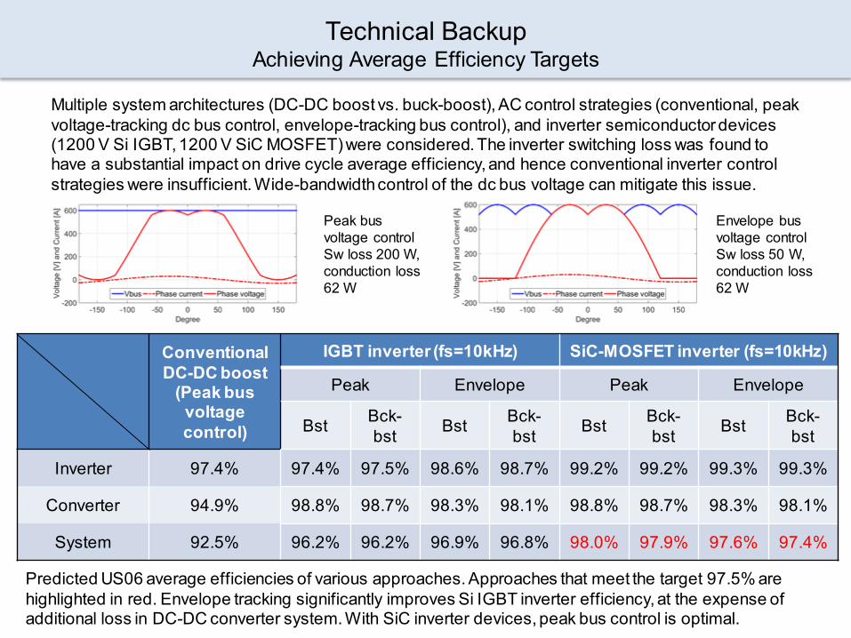
Technical BackupAchieving Average Efficiency Targets
Multiple system architectures (DC-DC boost vs. buck-boost), AC control strategies (conventional, peak voltage-tracking dc bus control, envelope-tracking bus control), and inverter semiconductor devices (1200 V Si IGBT, 1200 V SiC MOSFET) were considered. The inverter switching loss was found to have a substantial impact on drive cycle average efficiency, and hence conventional inverter control strategies were insufficient. Wide-bandwidth control of the dc bus voltage can mitigate this issue.
Peak bus voltage controlSw loss 200 W, conduction loss 62 W
Envelope bus voltage controlSw loss 50 W, conduction loss 62 W
System 92.5% 96.2% 96.2% 96.9% 96.8% 98.0% 97.9% 97.6% 97.4%
Predicted US06 average efficiencies of various approaches. Approaches that meet the target 97.5% are highlighted in red. Envelope tracking significantly improves Si IGBT inverter efficiency, at the expense of additional loss in DC-DC converter system. With SiC inverter devices, peak bus control is optimal.