A Formal Top-Down Design Process for Mixed-Signal Circuits April 2001 1 Cadence Design Systems, Inc. A Formal Top-Down Design Process for Mixed-Signal Circuits Ken Kundert Abstract With mixed-signal designs becoming more complex and time-to-market windows shrinking, designers cannot hope to keep up unless they change the way they design. They must adopt a more formal process for design and verification: top-down design. It involves more than simply a cursory design of the circuit block diagram before designing the blocks. Rather, it also involves developing and following a formal verification plan and an incremental and methodical approach for transforming the design from a abstract block diagram to a detailed transistor-level implementation. Author Dr. Ken Kundert is a fellow at Cadence Design Systems and for many years has been the principle architect of the Spectre circuit simulation family. As such, he led the development of Spectre, SpectreHDL, and SpectreRF, and initiated development of AMS Designer. He played a key role in the development of Agilent's harmonic balance simulator and made substantial contributions to both the Verilog-AMS and VHDL-AMS languages. He also authored two books on circuit simulation, Steady-State Methods for Simulating Analog and Microwave Circuits in 1990 and The Designer's Guide to SPICE and Spectre in 1995, as well as over two dozen papers published in refereed conferences and journals.
Transcript
A Formal Top-Down Design Process for Mixed-Signal Circuits April 20011
Cadence Design Systems, Inc.
A Formal Top-Down Design Process for Mixed-Signal Circuits
Ken Kundert
AbstractWith mixed-signal designs becoming more complex and time-to-market windows shrinking, designers cannot hope to keep up unless they change the way they design. They must adopt a more formal process for design and verification: top-down design. It involves more than simply a cursory design of the circuit block diagram before designing the blocks. Rather, it also involves developing and following a formal verification plan and an incremental and methodical approach for transforming the design from a abstract block diagram to a detailed transistor-level implementation.
AuthorDr. Ken Kundert is a fellow at Cadence Design Systems and for many years has been the principle architect of the Spectre circuit simulation family. As such, he led the development of Spectre, SpectreHDL, and SpectreRF, and initiated development of AMS Designer. He played a key role in the development of Agilent's harmonic balance simulator and made substantial contributions to both the Verilog-AMS and VHDL-AMS languages. He also authored two books on circuit simulation, Steady-State Methods for Simulating Analog and Microwave Circuits in 1990 and The Designer's Guide to SPICE and Spectre in 1995, as well as over two dozen papers published in refereedconferences and journals.
A Formal Top-Down Design Process for Mixed-Signal Circuits April 20012
2
Top-
Down
Des
ign
of M
ixed-
Sign
al C
ircui
ts
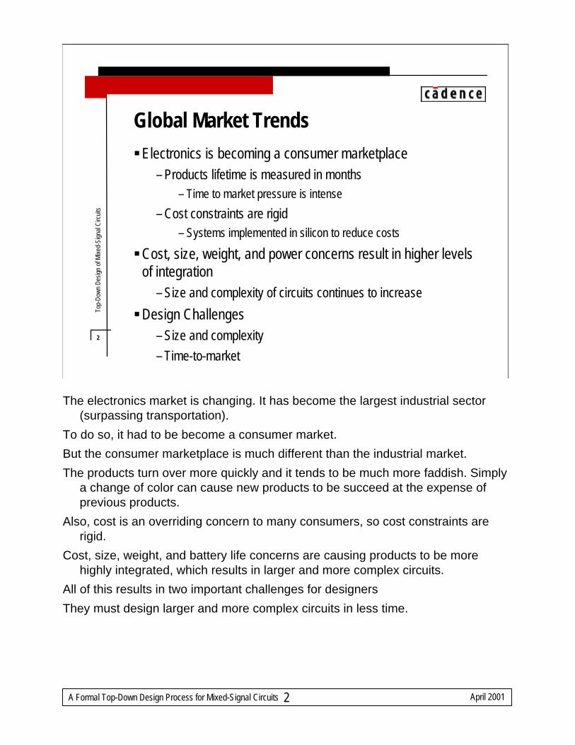
Global Market Trends§Electronics is becoming a consumer marketplace
– Products lifetime is measured in months– Time to market pressure is intense
– Cost constraints are rigid– Systems implemented in silicon to reduce costs
§Cost, size, weight, and power concerns result in higher levels of integration
– Size and complexity of circuits continues to increase
§Design Challenges– Size and complexity– Time-to-market
The electronics market is changing. It has become the largest industrial sector (surpassing transportation).
To do so, it had to be become a consumer market.
But the consumer marketplace is much different than the industrial market.
The products turn over more quickly and it tends to be much more faddish. Simply a change of color can cause new products to be succeed at the expense of previous products.
Also, cost is an overriding concern to many consumers, so cost constraints are rigid.
Cost, size, weight, and battery life concerns are causing products to be more highly integrated, which results in larger and more complex circuits.
All of this results in two important challenges for designers
They must design larger and more complex circuits in less time.
A Formal Top-Down Design Process for Mixed-Signal Circuits April 20013
3
Top-
Down
Des
ign
of M
ixed-
Sign
al C
ircui
ts
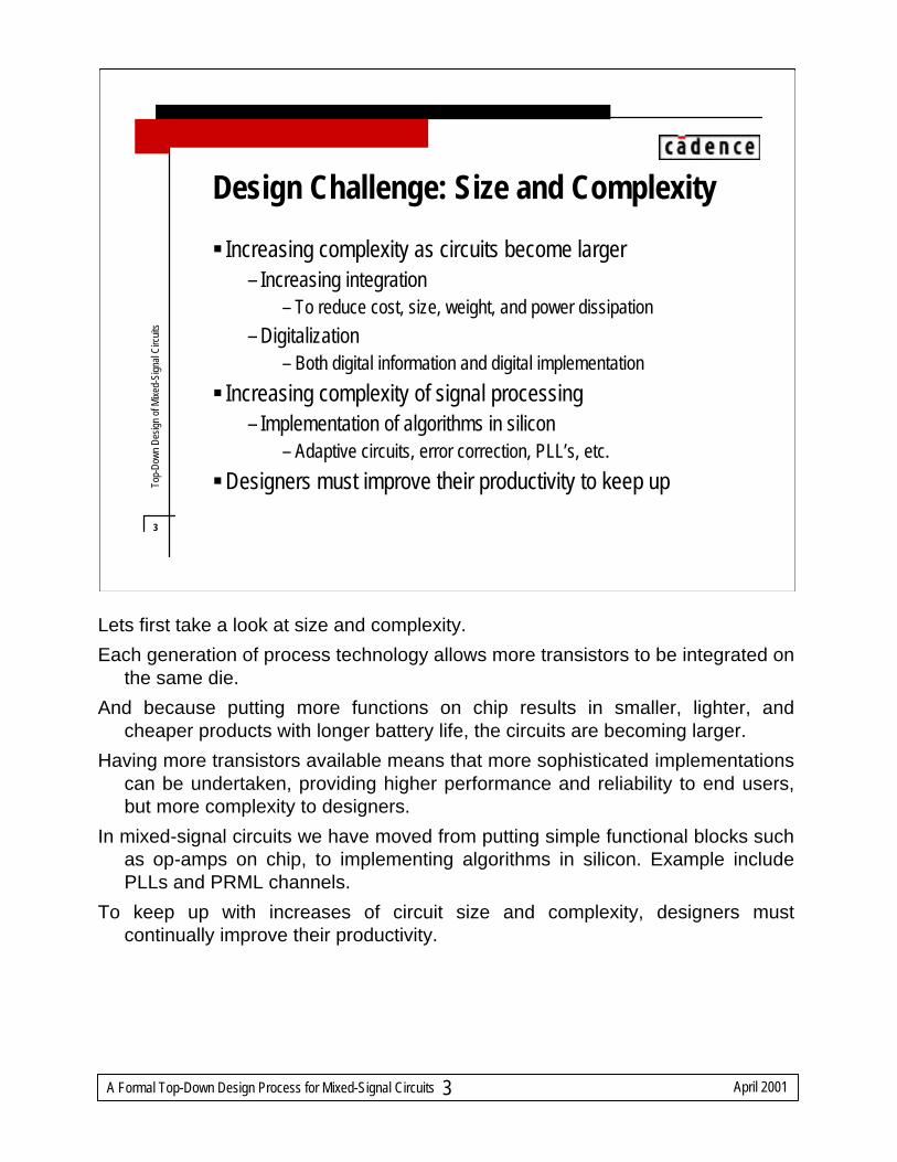
Design Challenge: Size and Complexity
§ Increasing complexity as circuits become larger– Increasing integration
– To reduce cost, size, weight, and power dissipation– Digitalization
– Both digital information and digital implementation
§ Increasing complexity of signal processing– Implementation of algorithms in silicon
– Adaptive circuits, error correction, PLL’s, etc.
§Designers must improve their productivity to keep up
Lets first take a look at size and complexity.
Each generation of process technology allows more transistors to be integrated on the same die.
And because putting more functions on chip results in smaller, lighter, and cheaper products with longer battery life, the circuits are becoming larger.
Having more transistors available means that more sophisticated implementations can be undertaken, providing higher performance and reliability to end users, but more complexity to designers.
In mixed-signal circuits we have moved from putting simple functional blocks such as op-amps on chip, to implementing algorithms in silicon. Example include PLLs and PRML channels.
To keep up with increases of circuit size and complexity, designers must continually improve their productivity.
A Formal Top-Down Design Process for Mixed-Signal Circuits April 20014
4
Top-
Down
Des
ign
of M
ixed-
Sign
al C
ircui
ts
Design Productivity GapTr
ansi
stor
s
1.0µ1990
0.18µ2000
0.5µ1995
Manufacturing Capability Gap
Design Capability
IC process technology is improving fasterthan IC design technology
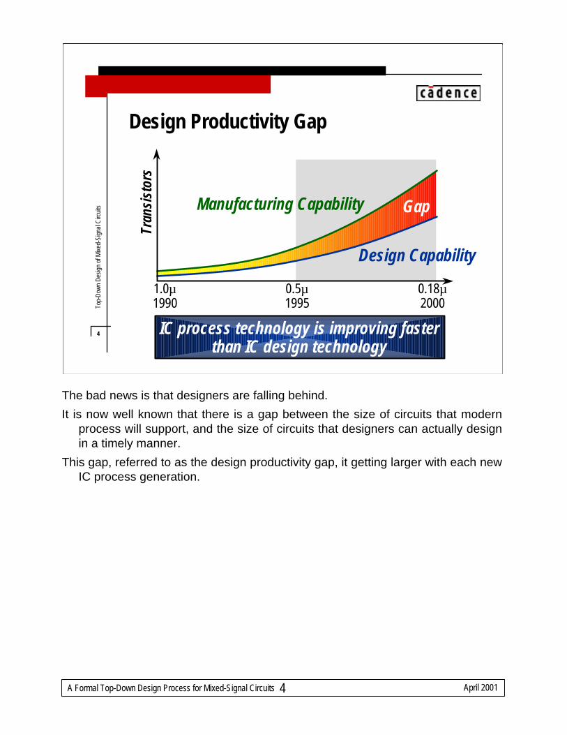
The bad news is that designers are falling behind.
It is now well known that there is a gap between the size of circuits that modern process will support, and the size of circuits that designers can actually design in a timely manner.
This gap, referred to as the design productivity gap, it getting larger with each new IC process generation.
A Formal Top-Down Design Process for Mixed-Signal Circuits April 20015
5
Top-
Down
Des
ign
of M
ixed-
Sign
al C
ircui
ts
Productivity: Improving CAD is not Enough
“Fundamental improvements in design methodology andCAD tools will be required to manage the
overwhelming design and verification complexity”
Dr. H. Samueli, co-chairman and CTO, Broadcom Corp. Invited Keynote Address, "Broadband communication ICs: enabling high-bandwidth connectivity in the home and office", Slide supplement 1999 to the Digest of Technical Papers, pp. 29-35, International Solid State Circuits Conference, Feb 15-17, 1999, San Francisco, CA
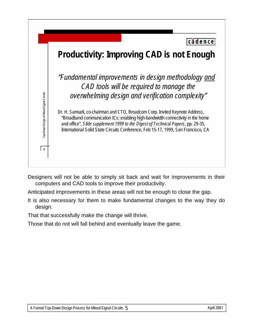
Designers will not be able to simply sit back and wait for improvements in their computers and CAD tools to improve their productivity.
Anticipated improvements in these areas will not be enough to close the gap.
It is also necessary for them to make fundamental changes to the way they do design.
That that successfully make the change will thrive.
Those that do not will fall behind and eventually leave the game.
A Formal Top-Down Design Process for Mixed-Signal Circuits April 20016
6
Top-
Down
Des
ign
of M
ixed-
Sign
al C
ircui
ts
Design Productivity
§14x productivity ratio between design groups (Collett International, 1998)
§ In a fast moving market– Cannot overcome this disparity in productivity by working harder– Must change the way design is done
§Reasons for poor productivity: Designers still using bottom-up design style
– Problems are found late in design cycle, causing substantial redesign– Simulation is expensive, and so usually inadequate– Inadequate verification requires silicon prototypes– Today’s designs are too complex for bottom-up design style
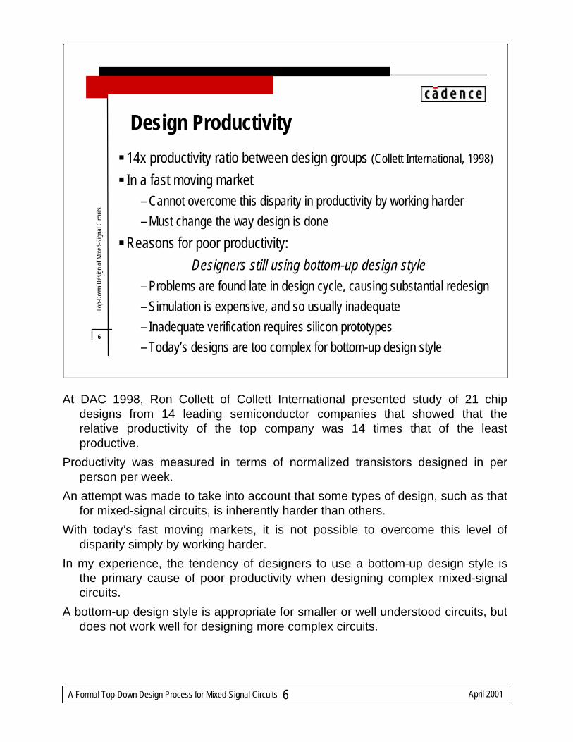
At DAC 1998, Ron Collett of Collett International presented study of 21 chip designs from 14 leading semiconductor companies that showed that the relative productivity of the top company was 14 times that of the least productive.
Productivity was measured in terms of normalized transistors designed in per person per week.
An attempt was made to take into account that some types of design, such as that for mixed-signal circuits, is inherently harder than others.
With today’s fast moving markets, it is not possible to overcome this level of disparity simply by working harder.
In my experience, the tendency of designers to use a bottom-up design style is the primary cause of poor productivity when designing complex mixed-signal circuits.
A bottom-up design style is appropriate for smaller or well understood circuits, but does not work well for designing more complex circuits.
A Formal Top-Down Design Process for Mixed-Signal Circuits April 20017
7
Top-
Down
Des
ign
of M
ixed-
Sign
al C
ircui
ts
Design Challenge: Time-to-Market
§Reduced time-to-market required by …– Stiff competition– Shrinking product lifetimes
§First to market generally captures the lion’s share of market– Assuming an innovative and well-designed product
§Timely follow-ons keep competitors at bay– New features– Reduced prices
Stiff competition and shrinking product lifetimes are requiring design groups to get their products to market more quickly.
Those that do not risk dramatically lower returns.
The first to market with an innovative and well-designed product generally captures the lion’s share of the market.
Timely releases of follow-on products with new features and reduced prices keeps competitors at bay.
A Formal Top-Down Design Process for Mixed-Signal Circuits April 20018
8
Top-
Down
Des
ign
of M
ixed-
Sign
al C
ircui
ts
Effect on Return of Being Late to Market
Efficient and Timely Inefficient and Untimely Inefficient but Timely
$
time
Incremental Investment and Return
$
time
Accumulated Investment and Return
Timely delivery results in much higher return, so ...it is better to invest heavily rather than risk being late
0
10
20
30
40
50
60
70
80
90
100
Return
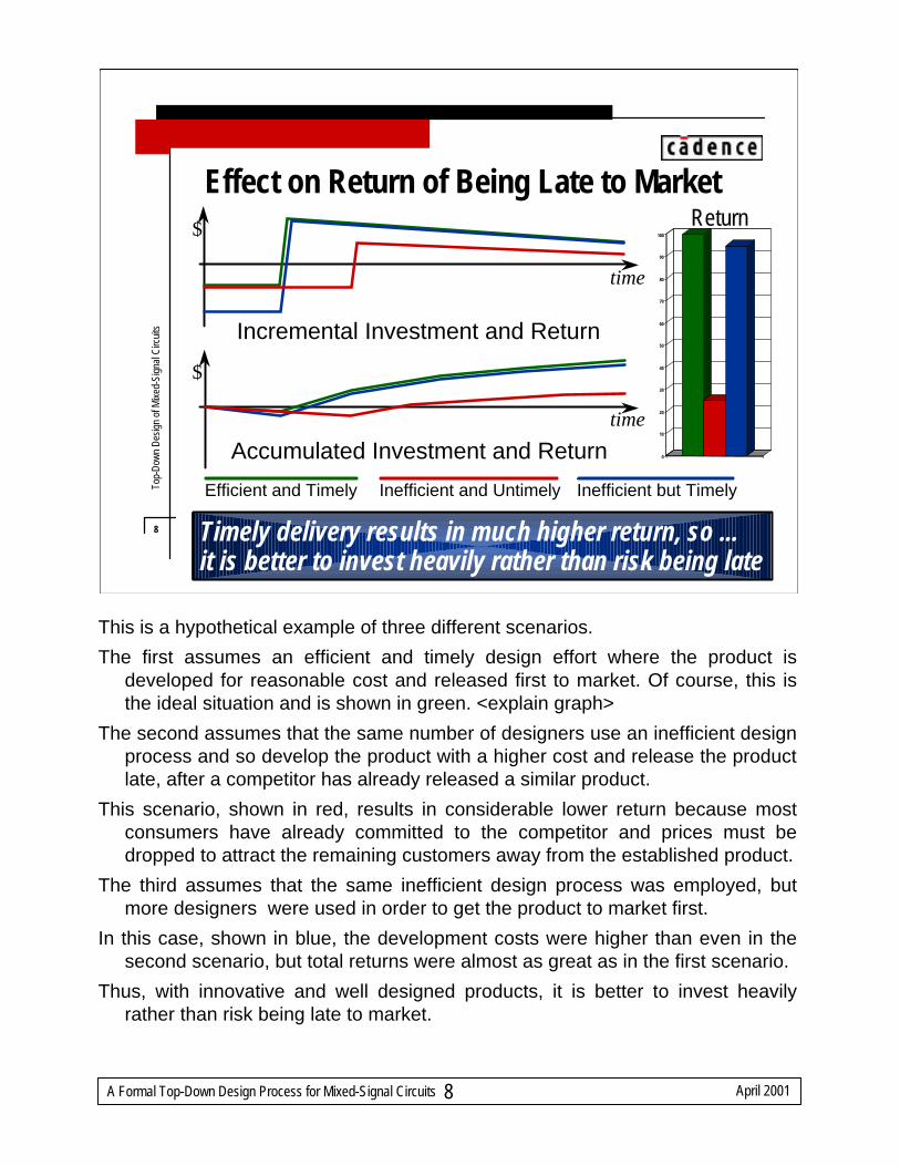
This is a hypothetical example of three different scenarios.
The first assumes an efficient and timely design effort where the product is developed for reasonable cost and released first to market. Of course, this is the ideal situation and is shown in green. <explain graph>
The second assumes that the same number of designers use an inefficient design process and so develop the product with a higher cost and release the product late, after a competitor has already released a similar product.
This scenario, shown in red, results in considerable lower return because most consumers have already committed to the competitor and prices must be dropped to attract the remaining customers away from the established product.
The third assumes that the same inefficient design process was employed, but more designers were used in order to get the product to market first.
In this case, shown in blue, the development costs were higher than even in the second scenario, but total returns were almost as great as in the first scenario.
Thus, with innovative and well designed products, it is better to invest heavily rather than risk being late to market.
A Formal Top-Down Design Process for Mixed-Signal Circuits April 20019
9
Top-
Down
Des
ign
of M
ixed-
Sign
al C
ircui
ts
What is Needed
§To handle larger and more complex circuits– Need better productivity– Need divide and conquer strategy
§To address time-to-market– Must effectively utilize more designers– Must reorganize design process
– More independent tasks– Reduce number of serial steps
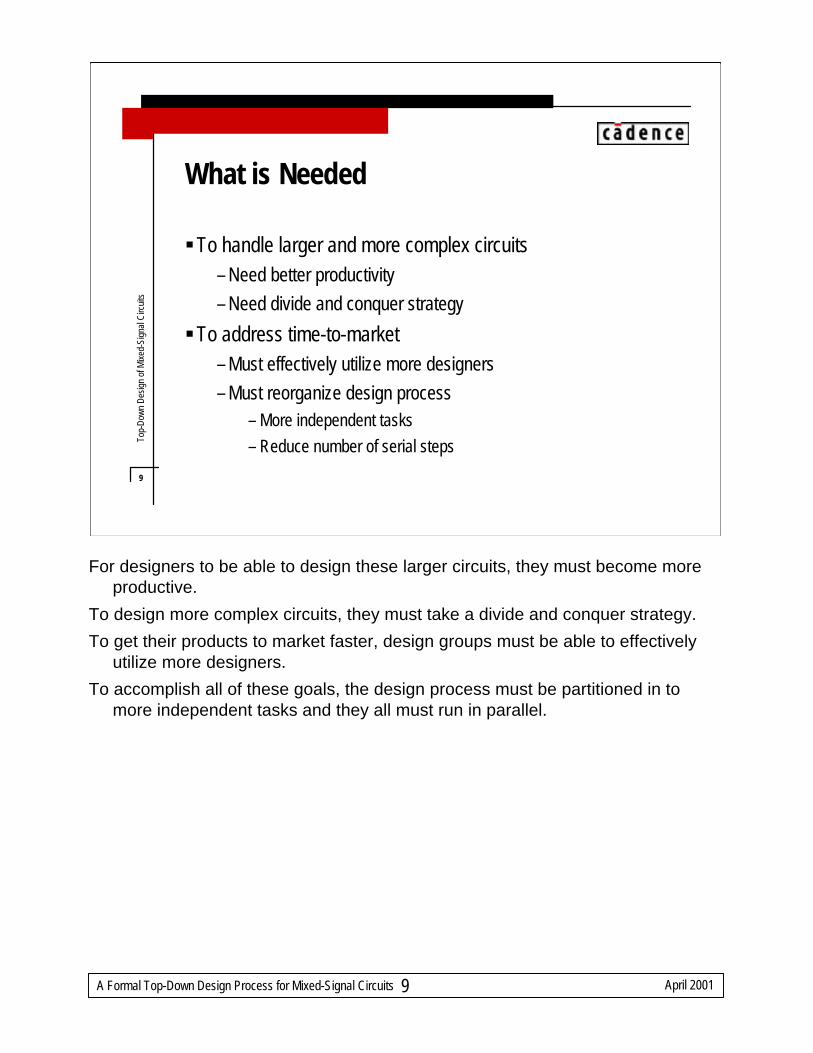
For designers to be able to design these larger circuits, they must become more productive.
To design more complex circuits, they must take a divide and conquer strategy.
To get their products to market faster, design groups must be able to effectively utilize more designers.
To accomplish all of these goals, the design process must be partitioned in to more independent tasks and they all must run in parallel.
A Formal Top-Down Design Process for Mixed-Signal Circuits April 200110
10
Top-
Down
Des
ign
of M
ixed-
Sign
al C
ircui
ts
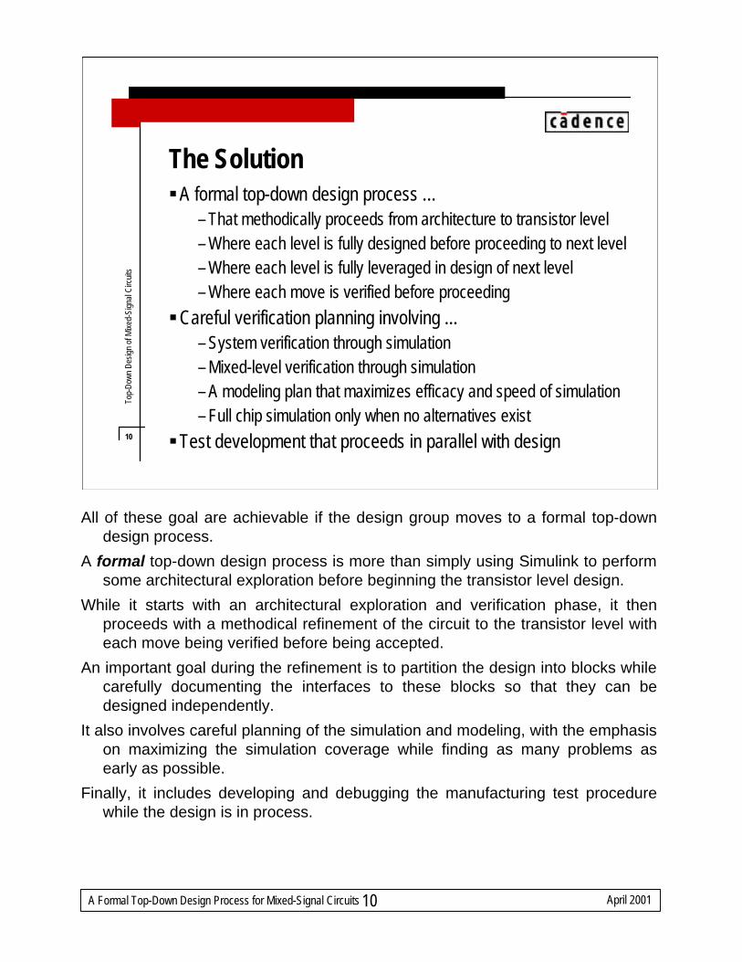
The Solution§A formal top-down design process …
– That methodically proceeds from architecture to transistor level– Where each level is fully designed before proceeding to next level– Where each level is fully leveraged in design of next level– Where each move is verified before proceeding
§Careful verification planning involving ...– System verification through simulation – Mixed-level verification through simulation– A modeling plan that maximizes efficacy and speed of simulation– Full chip simulation only when no alternatives exist
§Test development that proceeds in parallel with design
All of these goal are achievable if the design group moves to a formal top-down design process.
A formal top-down design process is more than simply using Simulink to perform some architectural exploration before beginning the transistor level design.
While it starts with an architectural exploration and verification phase, it then proceeds with a methodical refinement of the circuit to the transistor level with each move being verified before being accepted.
An important goal during the refinement is to partition the design into blocks while carefully documenting the interfaces to these blocks so that they can be designed independently.
It also involves careful planning of the simulation and modeling, with the emphasis on maximizing the simulation coverage while finding as many problems as early as possible.
Finally, it includes developing and debugging the manufacturing test procedure while the design is in process.
A Formal Top-Down Design Process for Mixed-Signal Circuits April 200111
11
Top-
Down
Des
ign
of M
ixed-
Sign
al C
ircui
ts
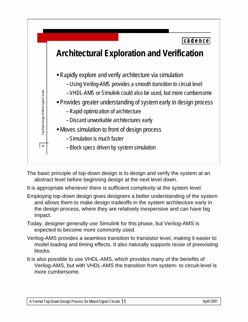
Architectural Exploration and Verification
§Rapidly explore and verify architecture via simulation– Using Verilog-AMS provides a smooth transition to circuit level– VHDL-AMS or Simulink could also be used, but more cumbersome
§Provides greater understanding of system early in design process– Rapid optimization of architecture– Discard unworkable architectures early
§Moves simulation to front of design process– Simulation is much faster– Block specs driven by system simulation
The basic principle of top-down design is to design and verify the system at an abstract level before beginning design at the next level down.
It is appropriate whenever there is sufficient complexity at the system level.
Employing top-down design gives designers a better understanding of the systemand allows them to make design tradeoffs in the system architecture early in the design process, where they are relatively inexpensive and can have big impact.
Today, designer generally use Simulink for this phase, but Verilog-AMS is expected to become more commonly used.
Verilog-AMS provides a seamless transition to transistor level, making it easier to model loading and timing effects. It also naturally supports reuse of preexisting blocks.
It is also possible to use VHDL-AMS, which provides many of the benefits of Verilog-AMS, but with VHDL-AMS the transition from system- to circuit-level is more cumbersome.
A Formal Top-Down Design Process for Mixed-Signal Circuits April 200112
12
Top-
Down
Des
ign
of M
ixed-
Sign
al C
ircui
ts
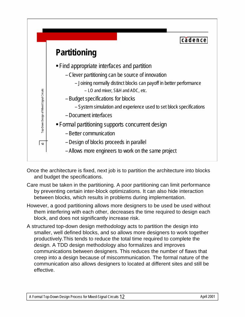
Partitioning§Find appropriate interfaces and partition
– Clever partitioning can be source of innovation– Joining normally distinct blocks can payoff in better performance
– LO and mixer, S&H and ADC, etc.
– Budget specifications for blocks– System simulation and experience used to set block specifications
– Document interfaces
§Formal partitioning supports concurrent design– Better communication– Design of blocks proceeds in parallel– Allows more engineers to work on the same project
Once the architecture is fixed, next job is to partition the architecture into blocks and budget the specifications.
Care must be taken in the partitioning. A poor partitioning can limit performance by preventing certain inter-block optimizations. It can also hide interaction between blocks, which results in problems during implementation.
However, a good partitioning allows more designers to be used be used without them interfering with each other, decreases the time required to design each block, and does not significantly increase risk.
A structured top-down design methodology acts to partition the design into smaller, well defined blocks, and so allows more designers to work together productively.This tends to reduce the total time required to complete the design. A TDD design methodology also formalizes and improves communications between designers. This reduces the number of flaws that creep into a design because of miscommunication. The formal nature of the communication also allows designers to located at different sites and still be effective.
A Formal Top-Down Design Process for Mixed-Signal Circuits April 200113
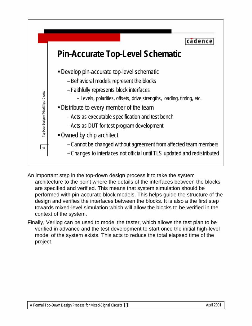
– Levels, polarities, offsets, drive strengths, loading, timing, etc.
§Distribute to every member of the team– Acts as executable specification and test bench– Acts as DUT for test program development
§Owned by chip architect– Cannot be changed without agreement from affected team members– Changes to interfaces not official until TLS updated and redistributed
An important step in the top-down design process it to take the system architecture to the point where the details of the interfaces between the blocks are specified and verified. This means that system simulation should be performed with pin-accurate block models. This helps guide the structure of the design and verifies the interfaces between the blocks. It is also a the first step towards mixed-level simulation which will allow the blocks to be verified in the context of the system.
Finally, Verilog can be used to model the tester, which allows the test plan to be verified in advance and the test development to start once the initial high-level model of the system exists. This acts to reduce the total elapsed time of the project.
A Formal Top-Down Design Process for Mixed-Signal Circuits April 200114
14
Top-
Down
Des
ign
of M
ixed-
Sign
al C
ircui
ts
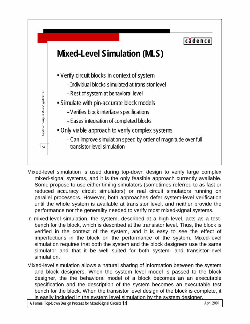
Mixed-Level Simulation (MLS)
§Verify circuit blocks in context of system– Individual blocks simulated at transistor level– Rest of system at behavioral level
§Simulate with pin-accurate block models– Verifies block interface specifications– Eases integration of completed blocks
§Only viable approach to verify complex systems– Can improve simulation speed by order of magnitude over full
transistor level simulation
Mixed-level simulation is used during top-down design to verify large complex mixed-signal systems, and it is the only feasible approach currently available. Some propose to use either timing simulators (sometimes referred to as fast or reduced accuracy circuit simulators) or real circuit simulators running on parallel processors. However, both approaches defer system-level verification until the whole system is available at transistor level, and neither provide the performance nor the generality needed to verify most mixed-signal systems.
In mixed-level simulation, the system, described at a high level, acts as a test-bench for the block, which is described at the transistor level. Thus, the block is verified in the context of the system, and it is easy to see the effect of imperfections in the block on the performance of the system. Mixed-level simulation requires that both the system and the block designers use the same simulator and that it be well suited for both system- and transistor-level simulation.
Mixed-level simulation allows a natural sharing of information between the system and block designers. When the system level model is passed to the block designer, the the behavioral model of a block becomes an an executable specification and the description of the system becomes an executable test bench for the block. When the transistor level design of the block is complete, it is easily included in the system level simulation by the system designer.
A Formal Top-Down Design Process for Mixed-Signal Circuits April 200115
15
Top-
Down
Des
ign
of M
ixed-
Sign
al C
ircui
ts
Simulation and Modeling Plans§ Identify areas of concern, develop verification plans
– Maximize use and efficacy of system-and mixed-level simulation– Minimize need for full-chip transistor-level simulation
§Modeling plan developed from simulation plan– There may be several models for each block
– Several simple models often better than one complex one– Consider loading, bias levels and headroom, etc.
§Developed and enforced by the chip architect§Up front planning results in ...
– More complete and efficient verification– Fewer design iterations
An important focus in a good top-down design methodology is the development of a comprehensive simulation and test plan. This is usually done by the systems architect once the architecture is developed and distributed. A formal planning process generally results in more efficient and more comprehensive simulation, meaning that more flaws are caught early and so there are fewer design iterations.
The simulation and test plans would initially be applied to the high-level description of the system, where they can be quickly debugged. Once available, they can be applied during the mixed-level simulations of the blocks, reducing the chance that errors will be found late in the design cycle.
A Formal Top-Down Design Process for Mixed-Signal Circuits April 200116
16
Top-
Down
Des
ign
of M
ixed-
Sign
al C
ircui
ts
SPICE Simulation
§Use selectively as needed– Mixed-level simulation
– Verify blocks in context of system
– Hot spots– Critical paths– Start-up behavior
§The idea is not to eliminate SPICE simulation, but to ...– Reduce the time spent in SPICE simulation while ...– Increasing the effectiveness of simulation in general
Circuits are getting more complex in two different ways at the same time. First, circuits are becoming larger. Consider wireless products. 30 years ago a typical transceiver contained between 5 and 10 transistors whereas it is common for a modern cell phone to contain between 1M and 10M transistors. Second, the operation of the circuits are becoming more complex. 20 years ago integrated circuits generally consisted of simple functional blocks such as opamps and gates. Verification typically required simulating the block for two or three cycles. Today, mixed-signal chips implement complex algorithms that require simulations to last thousands of cycles. Examples include PLLs, Σ∆converters, and magnetic storage PRML channels. Simulation complexity is increasing at a blistering pace, and verifying modern complex circuits completely at the transistor-level simply takes too much time, even for ‘fast’ simulators such as reduced accuracy simulators or those that employ parallel processing.
In a top-down design process, SPICE-level simulation is used judiciously in order to get the benefits without incurring the costs. All blocks are simulated at the transistor level in the context of the system in order to verify its functionality and interface. Hot spots, or areas of special concern, are identified up front and simulated at the transistor level. The performance of the circuit is verified by simulating just the signal path or key pieces of it at the transistor level. Finally, if start-up behavior is a concern, it is also simulated at the transistor level.
A Formal Top-Down Design Process for Mixed-Signal Circuits April 200117
17
Top-
Down
Des
ign
of M
ixed-
Sign
al C
ircui
ts
Reacting to Late Changes
§ Investment made in planning and modeling – Minimizes number of late changes– Allows quick response to late changes– HDL models, simulation and test plans, mixed-level simulation
already set up– Just change block and re-verify
Following a top-down design methodology also reduces the impact of changes that come late in the design cycle. If, for whatever reason, the circuit needs to be partially redesigned late in the design cycle, the infrastructure put in place as part of the methodology allows the change to be made quickly. The Verilog models can be updated and impact on the rest of system can be quickly checked. The simulation plan and the infrastructure for mixed-level simulations are already available and can be quickly applied to verify any changes.
A Formal Top-Down Design Process for Mixed-Signal Circuits April 200118
18
Top-
Down
Des
ign
of M
ixed-
Sign
al C
ircui
ts
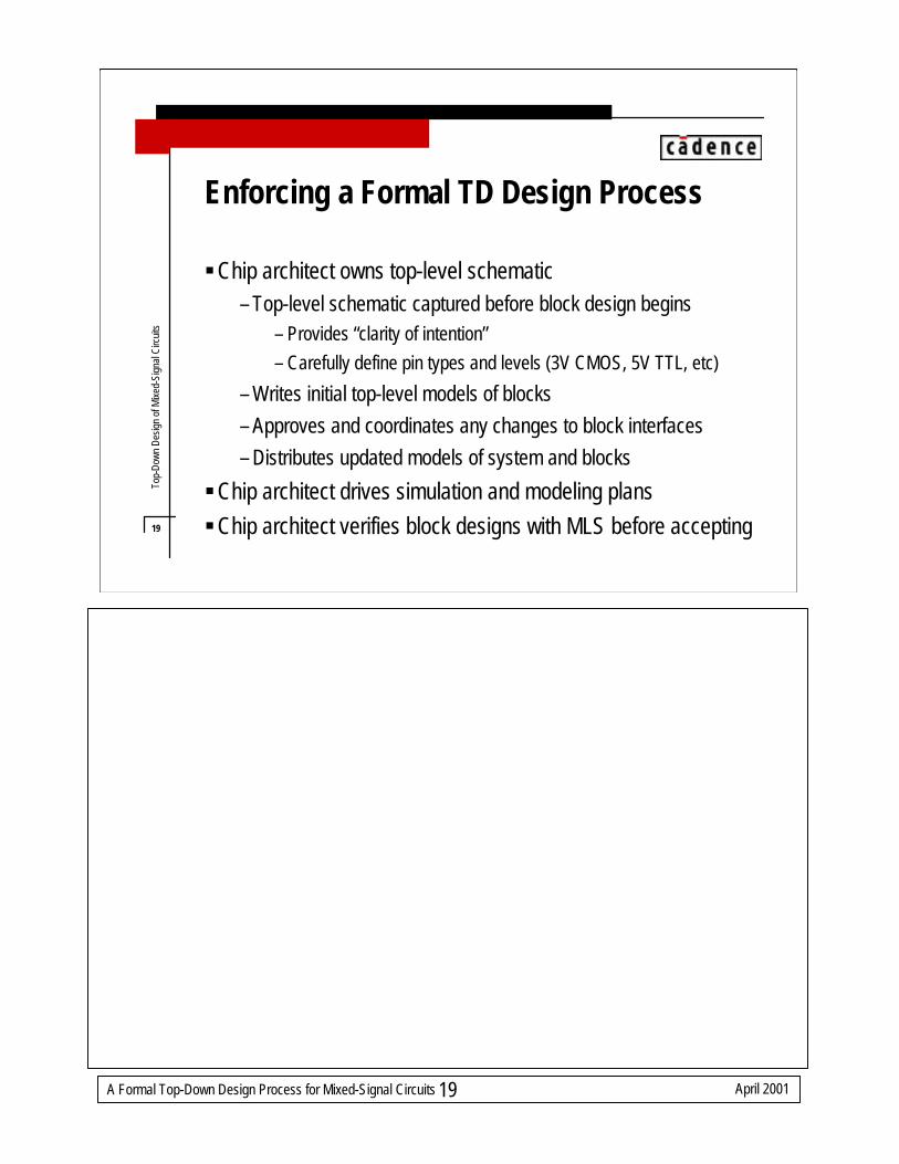
The Chip Architect
§Responsible for top-down design process– Must be knowledgeable of system and block design– Must be experienced
– Must anticipate problems to drive simulation and modeling plan
– Must be good at simulation and modeling– Write top-level models– Train block designers how to refine the models
§Systems engineer is often chip architect§Block designer should not be chip architect
– Block design has a way of consuming an engineer
A Formal Top-Down Design Process for Mixed-Signal Circuits April 200119
– Provides “clarity of intention”– Carefully define pin types and levels (3V CMOS, 5V TTL, etc)
– Writes initial top-level models of blocks– Approves and coordinates any changes to block interfaces– Distributes updated models of system and blocks
§Chip architect drives simulation and modeling plans§Chip architect verifies block designs with MLS before accepting
A Formal Top-Down Design Process for Mixed-Signal Circuits April 200120
20
Top-
Down
Des
ign
of M
ixed-
Sign
al C
ircui
ts
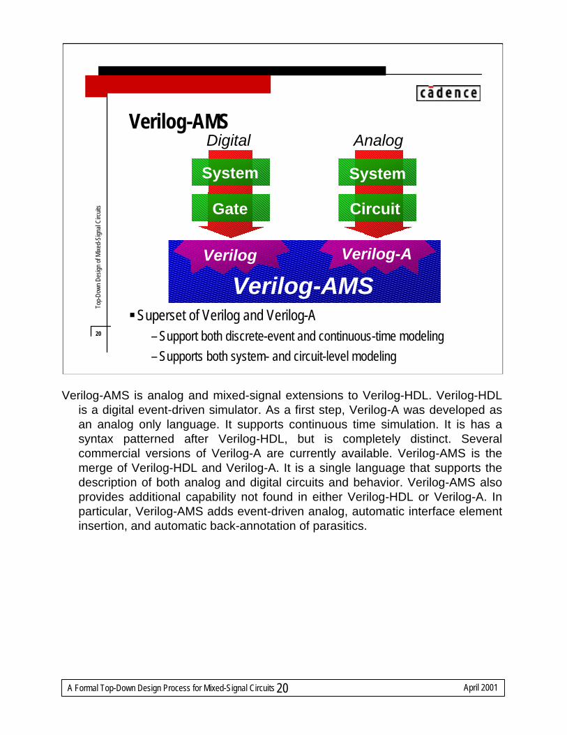
Digital Analog
System System
Gate Circuit
Verilog-AMSVerilog-AVerilog
Verilog-AMS
§Superset of Verilog and Verilog-A– Support both discrete-event and continuous-time modeling– Supports both system- and circuit-level modeling
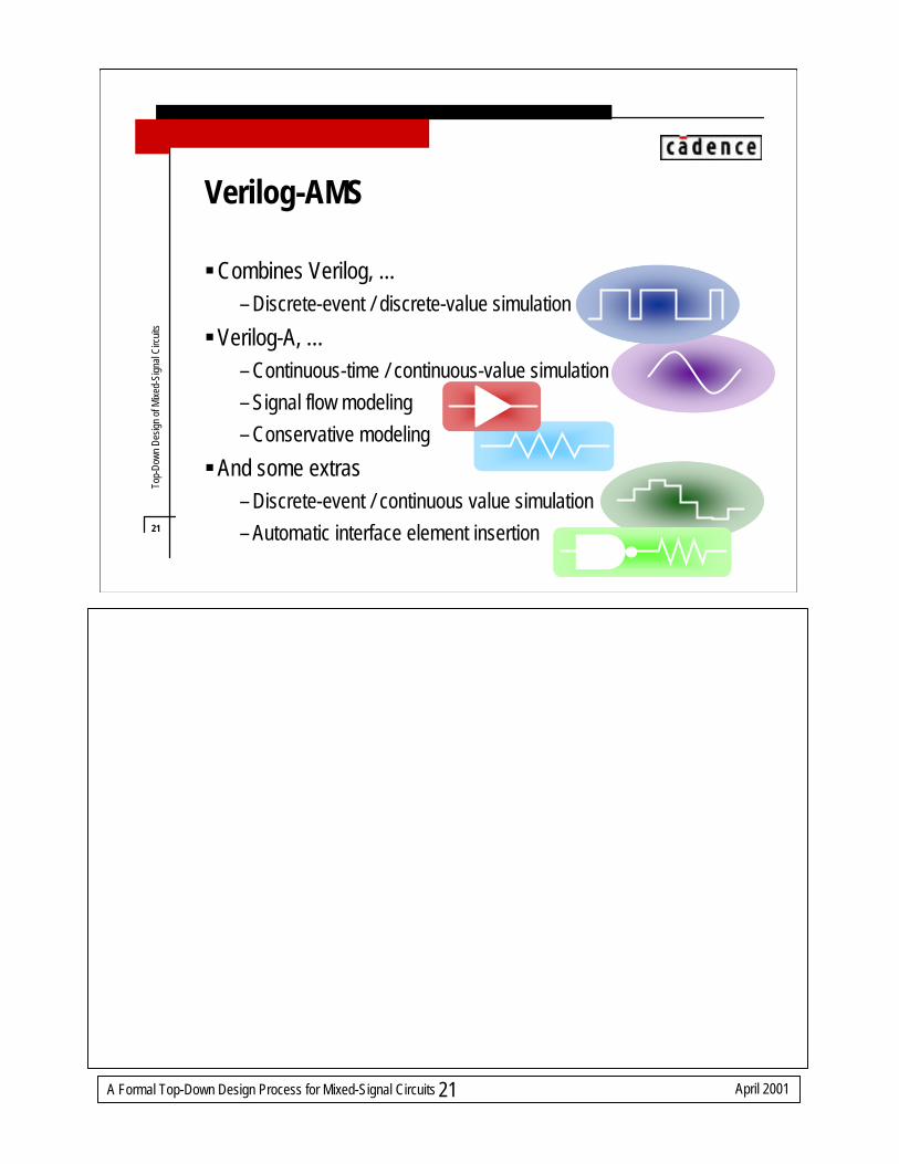
Verilog-AMS is analog and mixed-signal extensions to Verilog-HDL. Verilog-HDL is a digital event-driven simulator. As a first step, Verilog-A was developed as an analog only language. It supports continuous time simulation. It is has a syntax patterned after Verilog-HDL, but is completely distinct. Several commercial versions of Verilog-A are currently available. Verilog-AMS is the merge of Verilog-HDL and Verilog-A. It is a single language that supports the description of both analog and digital circuits and behavior. Verilog-AMS also provides additional capability not found in either Verilog-HDL or Verilog-A. In particular, Verilog-AMS adds event-driven analog, automatic interface element insertion, and automatic back-annotation of parasitics.
A Formal Top-Down Design Process for Mixed-Signal Circuits April 200121
§And some extras– Discrete-event / continuous value simulation– Automatic interface element insertion
A Formal Top-Down Design Process for Mixed-Signal Circuits April 200122
22
Top-
Down
Des
ign
of M
ixed-
Sign
al C
ircui
ts
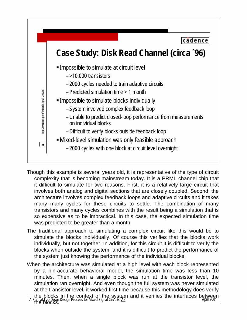
Case Study: Disk Read Channel (circa `96)§ Impossible to simulate at circuit level
– >10,000 transistors– 2000 cycles needed to train adaptive circuits– Predicted simulation time > 1 month
§ Impossible to simulate blocks individually– System involved complex feedback loop– Unable to predict closed-loop performance from measurements
on individual blocks– Difficult to verify blocks outside feedback loop
§Mixed-level simulation was only feasible approach– 2000 cycles with one block at circuit level overnight
Though this example is several years old, it is representative of the type of circuit complexity that is becoming mainstream today. It is a PRML channel chip that it difficult to simulate for two reasons. First, it is a relatively large circuit that involves both analog and digital sections that are closely coupled. Second, the architecture involves complex feedback loops and adaptive circuits and it takes many many cycles for these circuits to settle. The combination of many transistors and many cycles combines with the result being a simulation that is so expensive as to be impractical. In this case, the expected simulation time was predicted to be greater than a month.
The traditional approach to simulating a complex circuit like this would be to simulate the blocks individually. Of course this verifies that the blocks work individually, but not together. In addition, for this circuit it is difficult to verify the blocks when outside the system, and it is difficult to predict the performance of the system just knowing the performance of the individual blocks.
When the architecture was simulated at a high level with each block represented by a pin-accurate behavioral model, the simulation time was less than 10 minutes. Then, when a single block was run at the transistor level, the simulation ran overnight. And even though the full system was never simulated at the transistor level, it worked first time because this methodology does verify the blocks in the context of the system and it verifies the interfaces between the blocks.
A Formal Top-Down Design Process for Mixed-Signal Circuits April 200123
23
Top-
Down
Des
ign
of M
ixed-
Sign
al C
ircui
ts
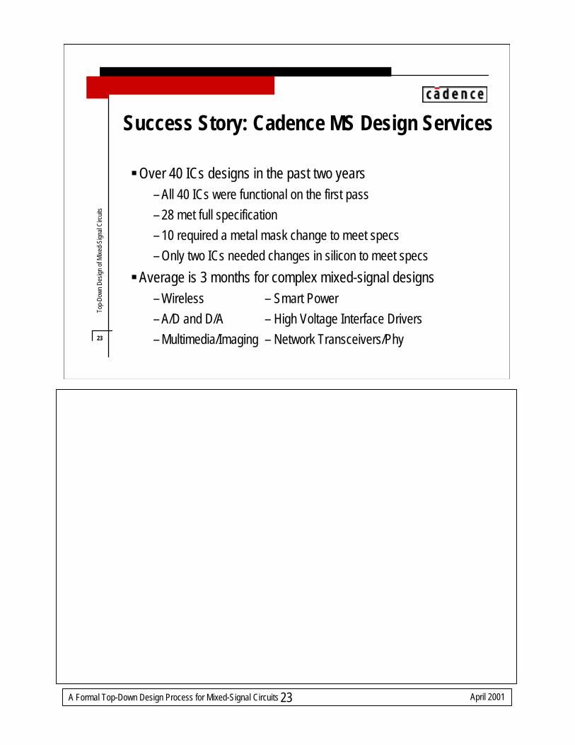
Success Story: Cadence MS Design Services
§Over 40 ICs designs in the past two years– All 40 ICs were functional on the first pass– 28 met full specification– 10 required a metal mask change to meet specs– Only two ICs needed changes in silicon to meet specs
§Average is 3 months for complex mixed-signal designs– Wireless – Smart Power – A/D and D/A – High Voltage Interface Drivers– Multimedia/Imaging – Network Transceivers/Phy
A Formal Top-Down Design Process for Mixed-Signal Circuits April 200124
24
Top-
Down
Des
ign
of M
ixed-
Sign
al C
ircui
ts
Top-Down Design Is ...
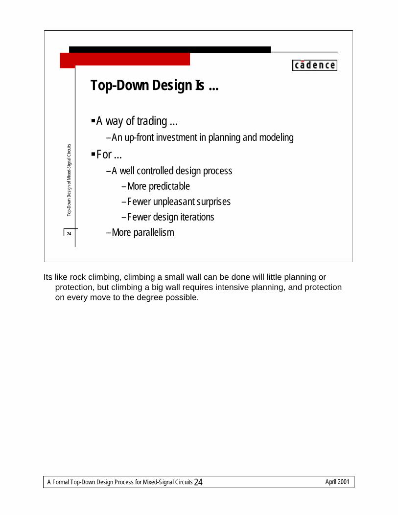
§A way of trading ...–An up-front investment in planning and modeling
Its like rock climbing, climbing a small wall can be done will little planning or protection, but climbing a big wall requires intensive planning, and protection on every move to the degree possible.
A Formal Top-Down Design Process for Mixed-Signal Circuits April 200125
25
Top-
Down
Des
ign
of M
ixed-
Sign
al C
ircui
ts
Top-Down Design ...
§ Is not going to happen on its own§ It is a formal top-down design process that requires a serious
commitment through out the entire design process
§ It requires a substantial investment in education and infrastructure§Any design group that attempts it without adequate training,
management support, and planning is likely to fail§ It is much easier the second time around
A Formal Top-Down Design Process for Mixed-Signal Circuits April 200126
26
A Formal Top-Down Design Process for Mixed-Signal Circuits April 200127
27
Top-
Down
Des
ign
of M
ixed-
Sign
al C
ircui
ts
Additional Points
§Top-down design leverages the experience of a few– It is important for the chip architect to be experienced– If so, the experience level of the block designers can be lower– Thus, one job of CA is to educate block designers
– How to model, how to simulate, what are system level issues
§CA need not anticipate which 2nd order effects are significant– Need only identify 2nd order effects that have potential of being
significant and then plan MLS to check
A Formal Top-Down Design Process for Mixed-Signal Circuits April 200128
28
Top-
Down
Des
ign
of M
ixed-
Sign
al C
ircui
ts
Additional Points
§You don’t have to model every effect. You could instead just putcode in that looks for bad situations and reports them (such as inappropriate bias points, circuits clipping, etc.)§The formal TDD approach may not find all problems, but may
find many much earlier in the design process, before the full chip simulations.§The roles of the chip architect need not be embodied in single
person. Instead, it represents a set of skills, duties, and responsibilities that must be present within the design group.