A local oscillator for WCDMA band VII based on frequency multiplication Andrea Gerosa • Andrea Bevilacqua • Andrea Neviani Received: 10 October 2011 / Revised: 23 January 2012 / Accepted: 27 January 2012 / Published online: 16 February 2012 Ó Springer Science+Business Media, LLC 2012 Abstract This work explores the generation of a local oscillator for WCDMA band VII based on frequency mul- tiplication of a GSM reference. The frequency multiplier is based on a PLL, which includes a compact VCO based on a ring oscillator. A proper PLL design allows to sufficiently reject the relative high VCO phase noise, complying with the WCDMA requirements. The effectiveness of the proposed approach is proved with the design of the whole multiplier in a 90 nm CMOS technology. The generated oscillation ran- ges from 3 to 6 GHz, while the simulated phase noise is -120 and -144 dBc/Hz at a frequency offset of 0.6 and 20 MHz, respectively, dissipating 6.3 mW. Keywords Frequency synthesizer Voltage controlled ring oscillator Multistandard wireless receivers WCDMA local oscillator 1 Introduction The interest for monolithic multistandard radio receivers is a matter of fact in modern communications. In the per- spective of aggressive system integration, a broad-band frequency synthesizer that generates the local oscillator (LO) at all the required frequencies is a key block of a multistandard transceiver [1–3]. However more efficient solutions can be envisioned, taking advantage of the fact that different standards call for frequency synthesizers with different specifications. Therefore one may prefer to design a high performance frequency synthesizer over a tighter bandwidth for the most demanding standard and then generate the other required LO with additional blocks. From this perspective, this work explores the potentials and the limits of generating a LO for the WCDMA band VII (from 2.5 to 2.69 GHz), starting from a GSM-compliant reference. The task requires frequency multiplication, hence the effectiveness of this approach depends on the possibility to realize a system whose complexity is much lower than a dedicated frequency synthesizer. We propose to realize the frequency multiplier using a PLL, whose VCO is based on a ring-oscillator, which is a good candidate for a compact solution with large tuning range. Since we can easily expect that a ring oscillator will have poor phase noise performance, the main contribution of this work is to prove the feasibility of a PLL that sufficiently rejects the VCO phase noise, in order to meet the WCDMA specifications that call for a phase noise level below 130 140dBc/Hz at a frequency off- set between few megahertz and tens of megahertz [2–4]. The PLL is described at the system level in Sect. 2. However the performance of the single basic blocks, espe- cially in terms of noise, strongly influences the minimum loop bandwidth required in order to meet the specification for the generated output signal. For this reason, a circuit implementation for each block has been singled out, as dis- cussed in Sect. 3, and the corresponding figures of merit have been extracted by means of transistor-level simulations, using the foundry models of a 90 nm CMOS technology. The design of the PLL is then finalized in Sect. 4, while the performance of the whole system is discussed in Sect. 5. 2 System description The block diagram of the proposed frequency multiplier is reported in Fig. 1: starting from the LO generated for the A. Gerosa (&) A. Bevilacqua A. Neviani Department of Information Engineering, University of Padova, Via Gradenigo, 6/b, 35131 Padova, Italy e-mail: [email protected]123 Analog Integr Circ Sig Process (2012) 72:111–119 DOI 10.1007/s10470-012-9839-2
Transcript
A local oscillator for WCDMA band VII based on frequencymultiplication
Andrea Gerosa • Andrea Bevilacqua •
Andrea Neviani
Received: 10 October 2011 / Revised: 23 January 2012 / Accepted: 27 January 2012 / Published online: 16 February 2012
� Springer Science+Business Media, LLC 2012
Abstract This work explores the generation of a local
oscillator for WCDMA band VII based on frequency mul-
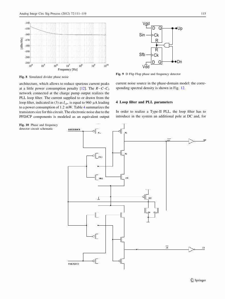
tiplication of a GSM reference. The frequency multiplier is
based on a PLL, which includes a compact VCO based on a
ring oscillator. A proper PLL design allows to sufficiently
reject the relative high VCO phase noise, complying with the
WCDMA requirements. The effectiveness of the proposed
approach is proved with the design of the whole multiplier in
a 90 nm CMOS technology. The generated oscillation ran-
ges from 3 to 6 GHz, while the simulated phase noise is
-120 and -144 dBc/Hz at a frequency offset of 0.6 and
20 MHz, respectively, dissipating 6.3 mW.
Keywords Frequency synthesizer � Voltage controlled
ring oscillator � Multistandard wireless receivers �WCDMA local oscillator
1 Introduction
The interest for monolithic multistandard radio receivers is
a matter of fact in modern communications. In the per-
spective of aggressive system integration, a broad-band
frequency synthesizer that generates the local oscillator
(LO) at all the required frequencies is a key block of a
multistandard transceiver [1–3]. However more efficient
solutions can be envisioned, taking advantage of the fact
that different standards call for frequency synthesizers with
different specifications. Therefore one may prefer to design
a high performance frequency synthesizer over a tighter
bandwidth for the most demanding standard and then
generate the other required LO with additional blocks.
From this perspective, this work explores the potentials
and the limits of generating a LO for the WCDMA band VII
(from 2.5 to 2.69 GHz), starting from a GSM-compliant
reference. The task requires frequency multiplication, hence
the effectiveness of this approach depends on the possibility
to realize a system whose complexity is much lower than a
dedicated frequency synthesizer. We propose to realize the
frequency multiplier using a PLL, whose VCO is based on a
ring-oscillator, which is a good candidate for a compact
solution with large tuning range. Since we can easily expect
that a ring oscillator will have poor phase noise performance,
the main contribution of this work is to prove the feasibility
of a PLL that sufficiently rejects the VCO phase noise, in
order to meet the WCDMA specifications that call for a phase
noise level below �130��140dBc/Hz at a frequency off-
set between few megahertz and tens of megahertz [2–4].
The PLL is described at the system level in Sect. 2.
However the performance of the single basic blocks, espe-
cially in terms of noise, strongly influences the minimum
loop bandwidth required in order to meet the specification
for the generated output signal. For this reason, a circuit
implementation for each block has been singled out, as dis-
cussed in Sect. 3, and the corresponding figures of merit have
been extracted by means of transistor-level simulations,
using the foundry models of a 90 nm CMOS technology. The
design of the PLL is then finalized in Sect. 4, while the
performance of the whole system is discussed in Sect. 5.
2 System description
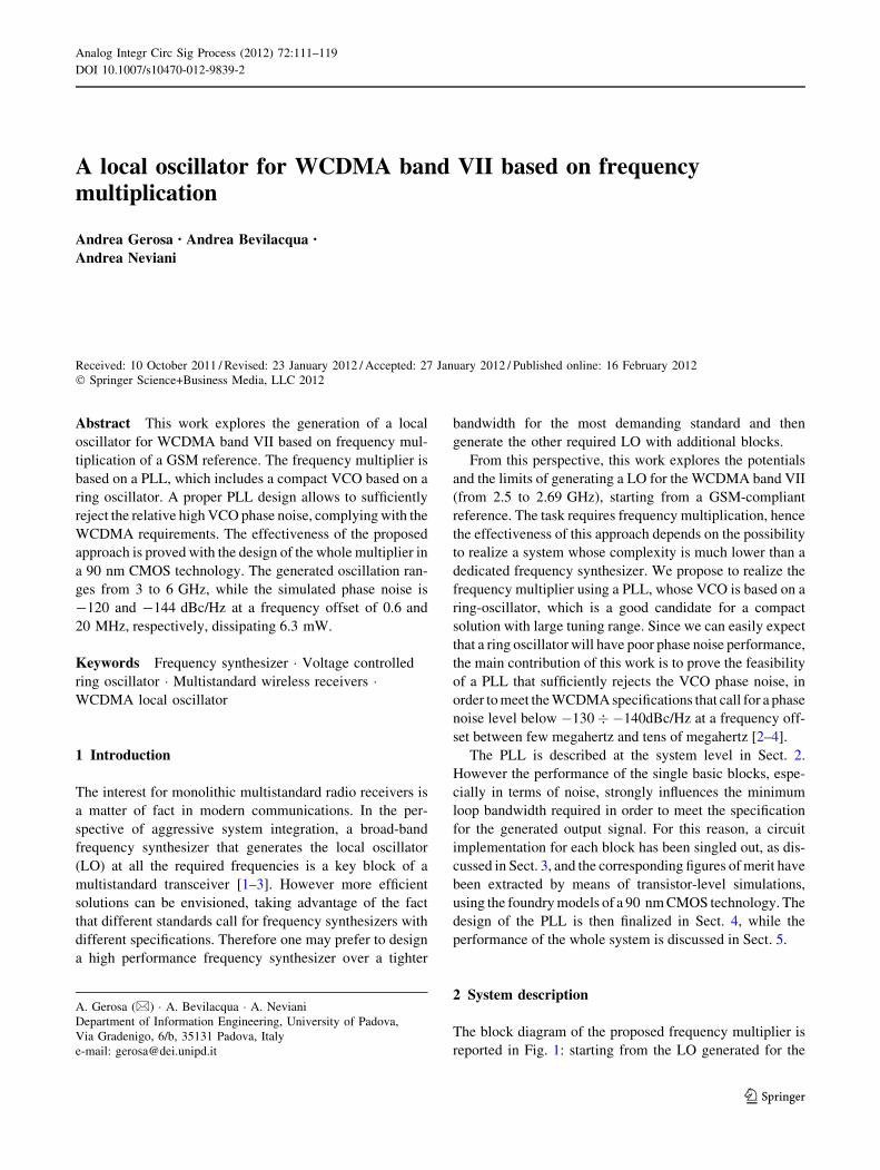
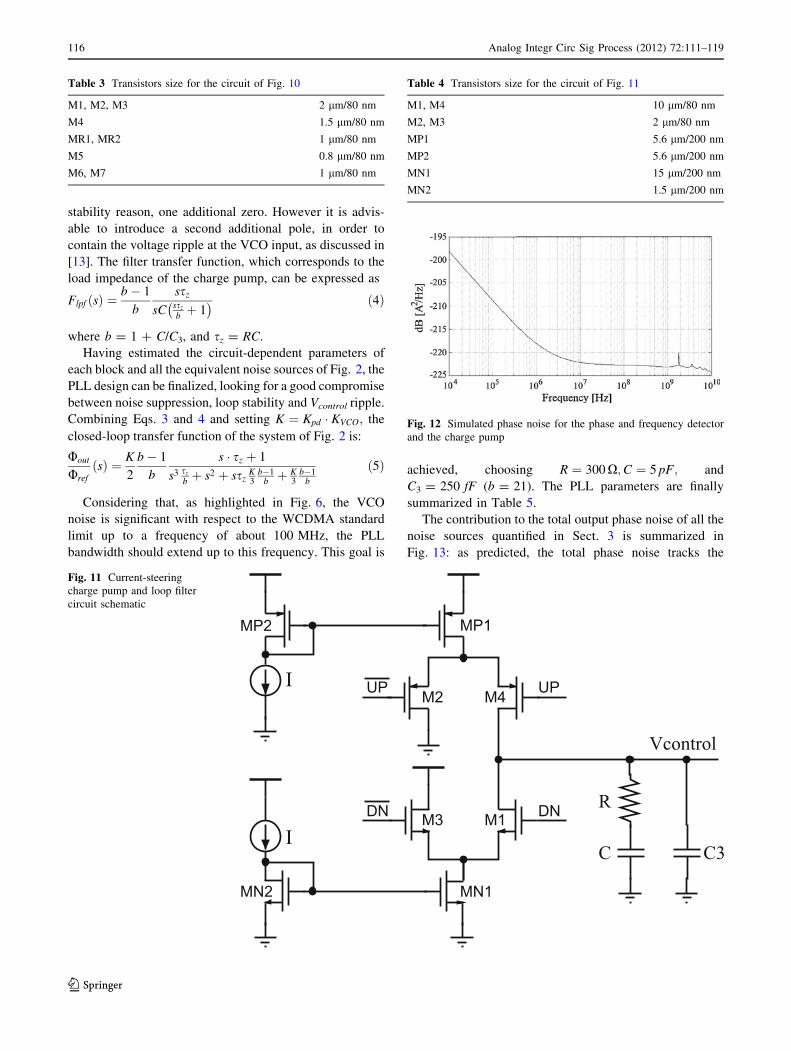
The block diagram of the proposed frequency multiplier is
reported in Fig. 1: starting from the LO generated for the
A. Gerosa (&) � A. Bevilacqua � A. Neviani
Department of Information Engineering, University of Padova,