May 20, 2014 Page 1 of 26 Sahu and Rincón-Mora Analog Integrated Circuits Laboratory Georgia Tech Analog Consortium School of Electrical and Computer Engineering Georgia Institute of Technology, Atlanta, GA 30332 USA E-mail: {bsahu, rincon-mora}@ece.gatech.edu Address for Correspondence Biranchinath Sahu 327434, Georgia Tech Station, Atlanta, GA 30332 Phone: 404-894-1299, Fax: 404-894-4641 E-mail: [email protected]Publication Information: This paper/part of the paper is not presented in any conference. ABSTRACT With the increasing use of low voltage portable devices and growing requirements of functionalities embedded into such devices, efficient power management techniques are needed for longer battery life time. Given the highly variable nature of batteries (e.g., 2.7−4.2 V for Li- ion), systems often require supply voltages to be both higher and lower than the battery voltage (e.g., power amplifier for CDMA applications), while supplying significant current, which is most efficiently generated by a non-inverting buck-boost switching converter. In this paper, the design and experimental results of a new dynamic, non-inverting, synchronous buck-boost converter for low voltage, portable applications is reported. The converter’s output voltage is dynamically adjustable (on-the-fly) from 0.4 to 4.0 V, while capable of supplying a maximum load current of 0.65 A from an input supply of 2.4−3.4 V. The worst-case response time of the converter for a 0.4 to 4 V step change in its output voltage (corresponding to a 0.2 to 2 V step at its reference input) is less than 300 μsec and to a load-current step of 0 to 0.5 A is within 200 μsec, yielding only a transient error of 40 mV in the output voltage. This paper also presents a A Low Voltage, Dynamic, Non-inverting, Synchronous Buck–Boost Converter for Portable Applications Biranchinath Sahu, Student Member, IEEE, and Gabriel A. Rincón-Mora, Senior Member, IEEE
Transcript
May 20, 2014 Page 1 of 26 Sahu and Rincón-Mora
Analog Integrated Circuits Laboratory Georgia Tech Analog Consortium
School of Electrical and Computer Engineering Georgia Institute of Technology, Atlanta, GA 30332 USA
E-mail: {bsahu, rincon-mora}@ece.gatech.edu Address for Correspondence Biranchinath Sahu 327434, Georgia Tech Station, Atlanta, GA 30332 Phone: 404-894-1299, Fax: 404-894-4641 E-mail: [email protected] Publication Information: This paper/part of the paper is not presented in any conference.
ABSTRACT
With the increasing use of low voltage portable devices and growing requirements of
functionalities embedded into such devices, efficient power management techniques are needed
for longer battery life time. Given the highly variable nature of batteries (e.g., 2.7−4.2 V for Li-
ion), systems often require supply voltages to be both higher and lower than the battery voltage
(e.g., power amplifier for CDMA applications), while supplying significant current, which is
most efficiently generated by a non-inverting buck-boost switching converter. In this paper, the
design and experimental results of a new dynamic, non-inverting, synchronous buck-boost
converter for low voltage, portable applications is reported. The converter’s output voltage is
dynamically adjustable (on-the-fly) from 0.4 to 4.0 V, while capable of supplying a maximum
load current of 0.65 A from an input supply of 2.4−3.4 V. The worst-case response time of the
converter for a 0.4 to 4 V step change in its output voltage (corresponding to a 0.2 to 2 V step at
its reference input) is less than 300 µsec and to a load-current step of 0 to 0.5 A is within 200
µsec, yielding only a transient error of 40 mV in the output voltage. This paper also presents a
A Low Voltage, Dynamic, Non-inverting, Synchronous Buck–Boost Converter for
Portable Applications Biranchinath Sahu, Student Member, IEEE, and Gabriel A. Rincón-Mora, Senior Member, IEEE
May 20, 2014 Page 2 of 26 Sahu and Rincón-Mora
non-mathematical, intuitive analysis of the time-averaged, small-signal model of a non-inverting
buck-boost converter.
Index Terms: Dynamic converter, non-inverting buck-boost converter, time-averaged modeling
I. INTRODUCTION
Current trends in consumer electronics demand progressively lower supply voltages due
to the unprecedented growth and use of wireless appliances. Portable devices, such as laptop
computers and personal communication devices require ultra low-power circuitry to enable
longer battery operation. The key to reducing power consumption while maintaining
computational throughput and quality of service is to use such systems at the lowest possible
supply voltage. The terminal voltage of the battery used in portable applications (e.g., NiMH,
NiCd, and Li-ion) varies considerably depending on the state of their charging condition. For
example, a single NiMH battery cell is fully charged to 1.8 V but it drops to 0.9 V before fully
discharged [1]. Therefore, systems designed for a nominal supply voltage (say, 1.5 V with a
single NiMH battery cell) require a converter capable of both stepping-up and stepping-down the
battery voltage.
While both buck (step-down) and boost (step-up) converters are widely used in power
management circuits, little attention has been given to integrated buck-boost converters for
portable applications. Inverting buck-boost converters and Cuk converters [2] are capable of
converting supply voltages to both higher and lower voltages, but the polarity of the output
voltage is opposite to the supply voltage. While these converters are suitable to generate the
required non-inverting buck-boost voltage with the battery terminals interchanged (i.e., positive
terminal connected to ground and negative terminal connected to the converter input supply), the
same battery cannot be used to supply power for other subsystems in a system-on-chip (SOC)
environment, thereby finding limited application. Isolated converter topologies such as Flyback
May 20, 2014 Page 3 of 26 Sahu and Rincón-Mora
converters [2], [3], are not suitable for low voltage, portable applications because they use a
transformer, which increases the board space and overall weight of the devices, not to mention
cost and poor efficiency. Alternatively, a boost converter followed by a linear regulator [4] can
be used for generating higher and lower voltages from a single supply. However, linear
regulators are considerably less efficient and not suitable for applications where load current is
high and battery lifetime is critical. Therefore, the only two plausible topologies left for
generating a voltage higher and lower than the supply are: (a) Non-inverting buck-boost
converter [2], [5], which is essentially achieved by cascading a buck with a boost converter, and
(b) Single-ended primary-inductance converter (SEPIC) [2]. The trend in portable applications is
to use the topologies that incorporate less number of external components and move closer to
cost effective SOC designs. Because SEPIC uses two inductors and two capacitors to transform
energy from the battery to the load, the single-inductor, non-inverting buck-boost converter,
irrespective of its complexity, is clearly the most suitable topology for a portable, cost-effective,
low-power environment. The ability to work over a wide range of input voltage to generate both
higher and lower voltages while supplying high current makes this topology an attractive choice
[6]. While the reported design in [5] is claimed to be the power industry’s first buck-boost
DC/DC converter [7], it’s ability to respond to dynamically adaptive reference control signal has
not been reported. Furthermore, the minimum output voltage of the converter is 2.5 V, which is
not suitable for applications requiring lower supply voltages.
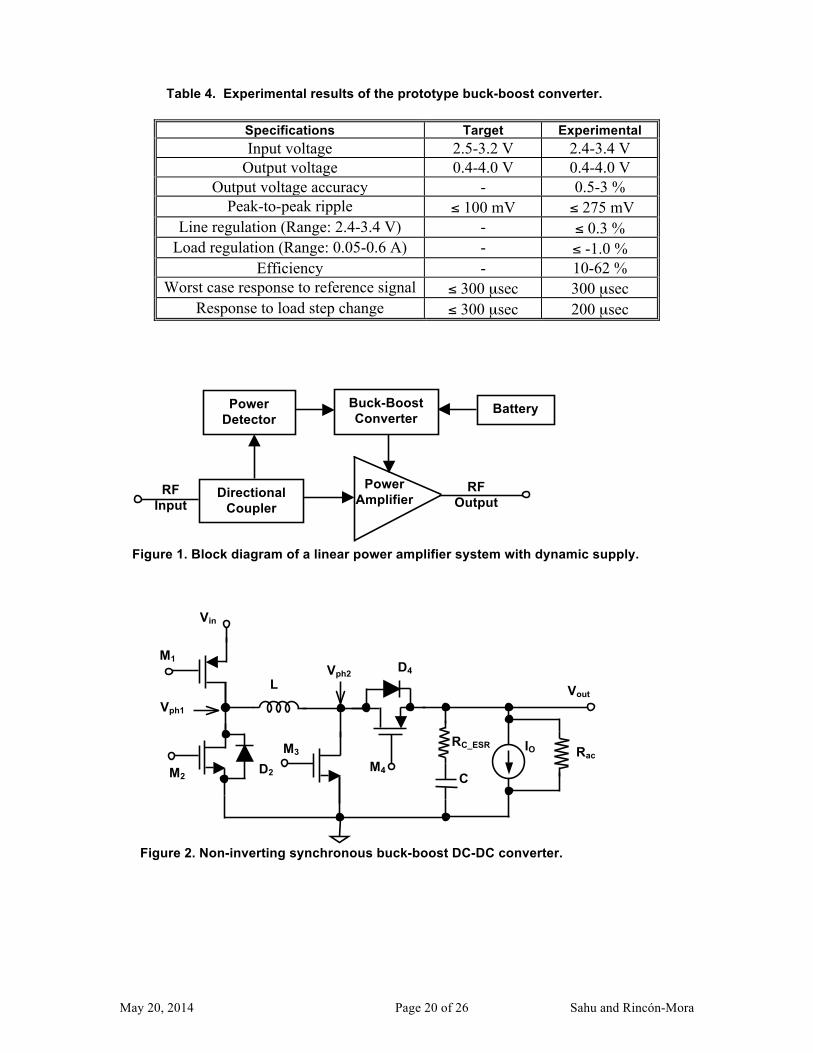
An application where non-inverting buck-boost converters are in high demand is
dynamically adaptive supplies for efficient, linear power amplifiers (PAs) in radio frequency
(RF) transceivers used for communicating with base stations in portable wireless devices [8]. To
prolong battery life, the power efficiency of the PA is improved by dynamically changing the
supply voltage and current, on-demand. An efficient linear PA scheme with a dynamic buck-
boost converter supply voltage is shown in Figure 1. The buck-boost converter, depending on a
May 20, 2014 Page 4 of 26 Sahu and Rincón-Mora
reference control signal adjusts the supply voltage to the PA. To implement closed-loop power
control in modern communication systems [9], based on its distance from the base station, the
transmitter adjusts the strength of the RF signal at the antenna. Since the gain of the PA is
constant for the entire output power range, depending on the input RF power, which is also
representative of the power handled by the PA, the reference control signal of the buck-boost
converter is generated –a detailed description of this scheme is found in [8]. Since the
transmitted power is adjusted in real time, a dynamically adaptive buck-boost converter is
required, the design and implementation of which is the subject of this paper. Other applications,
such as MPEG-4 codecs [10] and dynamic voltage scaling (DVS) processors [11] require
variable supply voltages, depending on the workload, to enable longer battery operation in
portable devices.
The paper is organized as follows. The single-inductor, non-inverting synchronous buck-
boost converter is discussed and its key waveforms are presented in Section II. In Section III, an
intuitive, non-mathematical explanation of the time-averaged small-signal model of the power
stage of the buck-boost converter is discussed. Analysis for different loading conditions and
design considerations, including stability and frequency compensation, of a voltage-mode buck-
boost converter are presented. Analytical expressions for critical power loss mechanisms in the
converter are highlighted. Section IV describes the details of the hardware design and
implementation of the experimental prototype converter. In Section V, results of the prototype
converter and discussions are offered. Finally, the paper is concluded in Section VI.
II. BACKGROUND
A non-inverting buck-boost converter is essentially a cascade combination of a buck
converter followed by a boost converter, where a single inductor-capacitor is used for both [2],
[6]. For low voltage implementations, the efficiency of the converter is improved by replacing
May 20, 2014 Page 5 of 26 Sahu and Rincón-Mora
the rectifier diodes with switches, which results in a synchronous converter topology. The
schematic of a synchronous buck-boost converter power stage is shown in Figure 2. The
notations used for the schematic are as follows: Vin = Supply voltage, Vout = Steady state output
voltage, IO = Output current, L = Inductor value, C = Capacitor value, RC_ESR = Equivalent series
resistance (ESR) of the capacitor, and Rac = Resistance of the load during change in output
voltage (ac condition). The key voltage and current waveforms of the converter are presented in
Figure 3.
During the TON period of the cycle, switches M1 and M3 are ON and the input voltage is
impressed across the inductor. Since the load current is instantaneously provided by the output
capacitor during this interval, the capacitor voltage (output voltage) decreases. During the other
interval of the switching period (TOFF), switches M2 and M4 are turned on and the inductor
energy is transferred to the output, providing both the load current and also charging the output
capacitor. There is a time delay (known as dead-time) between turning off M1, M3 and turning on
M2, M4 to prevent shoot-through current. During this period, the inductor current flows through
body diodes D2 and D4, from transistors M2 and M4, respectively. The duty cycle (D) of the
converter is given by:
TT
TTT
D ON
OFFON
ON =+
= , (1)
where T is the switching time period of the converter.
Since the node Vph1 is connected to Vin for DT time over a period of T, the average
voltage Vph1,avg = DVin. Similarly, the average node voltage of Vph2 can be given by Vph2,avg =
Dʹ′Vout (Dʹ′ = 1−D). Under steady-state operating condition, the inductor can be treated as short,
and the average voltage of Vph1 and Vph2 are equal
outin VDDV ʹ′= ⇒ D1D
VV
in
out
−= . (2)
May 20, 2014 Page 6 of 26 Sahu and Rincón-Mora
For the duty cycle of 0.5, the output voltage is equal to the input voltage. When duty cycle is
less than 0.5, the output voltage is lower than the input (buck mode), and for duty cycle greater
than 0.5, the output voltage is higher than the input (boost mode).
For low output voltages below the threshold voltage of the PMOS (M4 in the schematic),
the transistor never turns ON, leaving only the diode D4 as the switch resulting in asynchronous
operation of the converter, which is inefficient because of the large voltage drop across the body
diode. A transmission gate, which is a parallel combination of a PMOS and a NMOS with
complimentary logic inputs to their gates, can be used in place of PMOS boost transistor (M4) to
operate the converter in synchronous mode. For output voltages below the threshold voltage of
PMOS, the NMOS acts as switch, and for higher output voltages, NMOS turns-off while PMOS
act as a switch. For intermediate output voltages, both PMOS and NMOS of the transmission
gate remain ON to share the current during the switching interval in which the inductor is
connected to the output.
III. SYSTEM DESIGN CONSIDERATIONS III.A. Time-averaged Small-signal Model Intuitive Explanation
Feedback control system is employed in DC-DC converters to regulate the output
voltage, regardless of the changes in input voltage or loading conditions. To design the feedback
control loop of DC-DC switching regulators, an equivalent small-signal model of the power
stage is required that is valid for low frequency perturbation of the duty cycle. To model the
power stage of converters, techniques such as state-space averaging and circuit averaging [2],
[12] have been used extensively. However, the derivation is mathematically complex and
difficult to relate to intuitive operation. In this section, a time-averaged model for a synchronous
buck-boost converter power stage is explained intuitively with precise one-to-one mapping with
the operation of the circuit.
May 20, 2014 Page 7 of 26 Sahu and Rincón-Mora
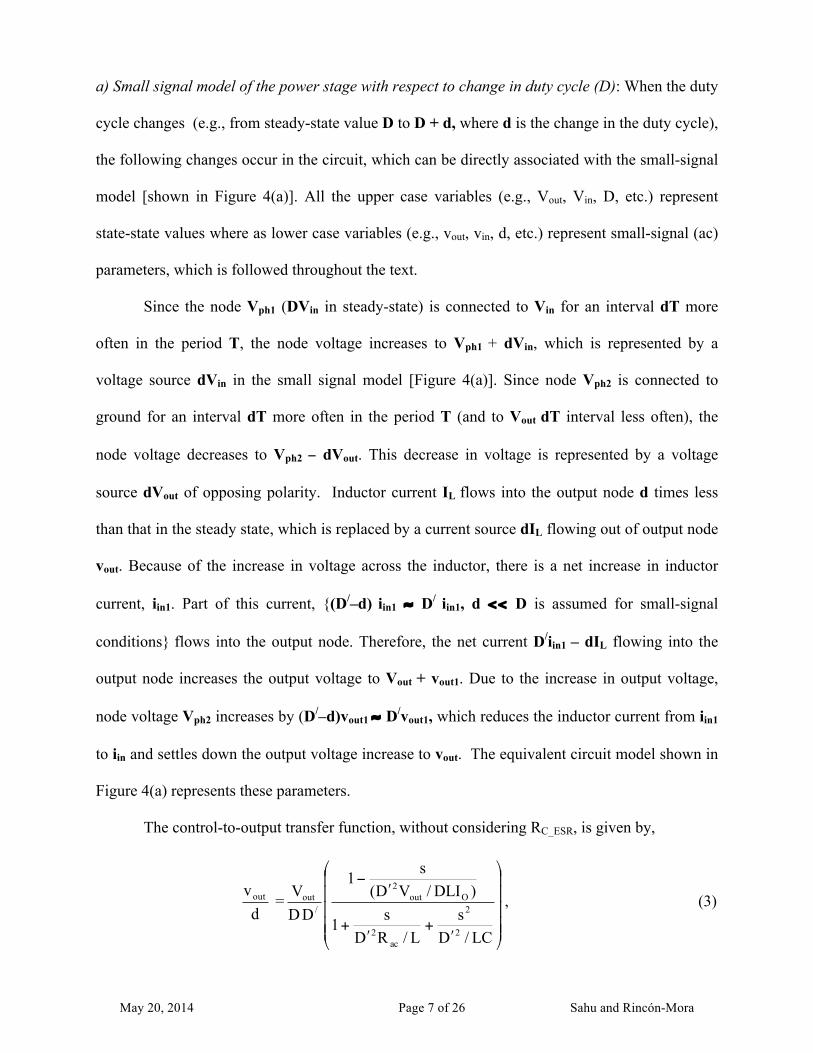
a) Small signal model of the power stage with respect to change in duty cycle (D): When the duty
cycle changes (e.g., from steady-state value D to D + d, where d is the change in the duty cycle),
the following changes occur in the circuit, which can be directly associated with the small-signal
model [shown in Figure 4(a)]. All the upper case variables (e.g., Vout, Vin, D, etc.) represent
state-state values where as lower case variables (e.g., vout, vin, d, etc.) represent small-signal (ac)
parameters, which is followed throughout the text.
Since the node Vph1 (DVin in steady-state) is connected to Vin for an interval dT more
often in the period T, the node voltage increases to Vph1 + dVin, which is represented by a
voltage source dVin in the small signal model [Figure 4(a)]. Since node Vph2 is connected to
ground for an interval dT more often in the period T (and to Vout dT interval less often), the
node voltage decreases to Vph2 − dVout. This decrease in voltage is represented by a voltage
source dVout of opposing polarity. Inductor current IL flows into the output node d times less
than that in the steady state, which is replaced by a current source dIL flowing out of output node
vout. Because of the increase in voltage across the inductor, there is a net increase in inductor
current, iin1. Part of this current, {(D/–d) iin1 ≈ D/ iin1, d << D is assumed for small-signal
conditions} flows into the output node. Therefore, the net current D/iin1 – dIL flowing into the
output node increases the output voltage to Vout + vout1. Due to the increase in output voltage,
node voltage Vph2 increases by (D/–d)vout1 ≈ D/vout1, which reduces the inductor current from iin1
to iin and settles down the output voltage increase to vout. The equivalent circuit model shown in
Figure 4(a) represents these parameters.
The control-to-output transfer function, without considering RC_ESR, is given by,
dvout =
⎟⎟⎟⎟⎟
⎠
⎞
⎜⎜⎜⎜⎜
⎝
⎛
ʹ′+
ʹ′+
ʹ′−
LC/Ds
L/RDs1
)DLI/VD(s1
DDV
2
2
ac2
Oout2
/out , (3)
May 20, 2014 Page 8 of 26 Sahu and Rincón-Mora
which is consistent with the equation for the inverting buck-boost converter [2].
b) Small-signal model of power stage with respect to change in line (input) voltage: When the
input voltage changes from Vin to Vin + vin, the following changes occur in the power stage
(Figure 2). Node voltage Vph1 increases by Dvin and can be represented by a voltage source
[Figure 4(b)]. Due to the increase in voltage across the inductor, the inductor current increases by
iin1, part of which flows into the output node as D/iin1, increasing the output voltage by vout1. The
increase in output voltage increases the node voltage Vph2 by D/vout1, which reduces the inductor
to iin, and ultimately settles down the output voltage to vout. These parameters are represented in
the equivalent circuit model shown in Figure 4(b).
The line-to-output transfer function, without considering RC_ESR, is given by,
in
out
vv =
⎟⎟⎟⎟⎟
⎠
⎞
⎜⎜⎜⎜⎜
⎝
⎛
ʹ′+
ʹ′+
LC/Ds
L/RDs1
1DD
2
2
ac2
/. (4)
Equations (3) and (4) are compared with the standard second order transfer function [2],
and expression for DC gain, poles and zeros are presented in Table 1. Also, the effect of the
output capacitor ESR, which introduces a left-half plane (LHP) zero in both the transfer
functions is shown.
III.B. Analysis of the transfer functions for different loads
The load at the converter output can vary significantly depending on the application. To
design the converter’s control-loop compensation that is stable across all loading conditions, the
transfer functions (derived earlier in Section III.A) are analyzed for the two extremes: (a) a pure
current source load with high ac output impedance, and (b) a simple resistive load with relatively
low impedance (equal to value of the resistor) to ensure stable control-loop compensation. For
loads with equal current, the ac impedance (Rac) modulates the quality factor (Q-factor) of the
May 20, 2014 Page 9 of 26 Sahu and Rincón-Mora
second-order denominator of both the transfer functions [Equations (3) and (4)] between the two
extremes identified. The gain and phase plots comparing the control-to-output transfer function
frequency response for the two loads are presented in Figure 5. The parameters used for
generating the plots are: D = 0.75, R = 10 Ω (resistive load), IO = 0.4 A (current source load), L =
3.0 V. For a resistive load, a change in the output voltage directly translates to a change in the
load current, thereby absorbing the extra energy during the peak, which is ultimately reflected as
degraded Q-factor. For a current-source load, a change in the output voltage does not affect its
current (because of its high impedance); consequently Q is higher. The real part of the complex-
conjugate poles, the right- and left-half plane (capacitor ESR zero) zeros remain unchanged
under both loading conditions.
III.C. Control Scheme and Frequency Compensation
While other controlling schemes [13] can be used for closed-loop control, voltage mode
was considered for this design because of its simplicity (no inductor current information is
required). Voltage-mode control enjoys popularity in the industry for simple, point-of-load DC-
DC converter applications [14]. As with the boost converter, the right-half plane (RHP) zero
limits the unity-gain frequency (UGF) of the closed-loop performance of the buck-boost
converter. Therefore, the RHP zero is designed to reside far beyond the UGF. Considering the
expression given in Table 1, the RHP zero is at the lowest frequency when the duty cycle is at its
peak, which corresponds to the highest output voltage value. For a specified Vout, load current IO,
and input voltage Vin combination, a smaller inductor pushes out the RHP zero, which results in
higher peak-current rating requirements for the switching devices and induces more RMS power
losses in the current-flowing path.
May 20, 2014 Page 10 of 26 Sahu and Rincón-Mora
Therefore, the compensation design depends on the location of the left-half plane (LHP)
zero arising as result of the ESR of the output capacitor. Feedback-loop compensation design for
the two cases: (a) when the ESR zero is located within the desired UGF and (b) when the ESR
zero is far from the desired UGF have been explained in [3], [15]. Since the location of the
transfer function poles and zeros vary with the duty cycle, the converter is compensated for the
lowest frequency poles and zeros, which occurs when the duty cycle is at its peak.
III.D. Duty-Cycle Limiting
During start-up and transient (load and control voltage) events, the duty cycle changes
between extremes. For example, during start-up, the reference voltage can be higher than the
feedback voltage, especially if considering an independent, dynamic voltage reference.
Consequently, the error amplifier’s output goes to the positive rail, in other words, equal to or
greater than the peak sawtooth voltage, which results in the PWM comparator’s output reaching
the negative rail throughout the entire switching period. The transistors M1 and M3 (Figure 2)
are therefore turned on, impressing the input voltage upon the inductor. The inductor current
never flows into the output during this interval; therefore, the output voltage remains unchanged.
However, the inductor current continues to increase until the resistance of the path limits it, but
such a high current can damage the inductor and power switches, even before reaching the limit.
This phenomenon is avoided by choosing the positive rail supply voltage of the error amplifier to
be less than the peak value of the sawtooth waveform, as shown in Figure 6, thereby limiting the
duty cycle to less than unity.
III.E. Dead-time Control
Dead-time control in synchronous converters is required to prevent “shoot-through
current” which is an unnecessary power loss resulting when the rectifier and pass transistors are
both conducting current simultaneously. A simple fixed-delay dead-time control scheme is
adopted for the discrete prototype presented. The schematic of the control scheme and the
May 20, 2014 Page 11 of 26 Sahu and Rincón-Mora
relevant waveforms are shown in Figure 7. The delay time of the logic gates 1 and 2, δ, is
assumed to be much larger than signal delay in the power transistors and in gate 3. In the
prototype implementation, RC circuits are used in conjunction with logic gates 1 and 2 to realize
these delays. Advanced schemes (e.g., adaptive and predictive dead-time controls [16]) may be
implemented to reduce body-diode conduction, gate- drive and switching losses in the converter.
III.F. Power Loss Analysis
Theoretical estimation of power losses in the converter is required to determine the
efficiency limit and improve its efficiency further using power saving techniques. Mathematical
expressions for power loss mechanisms in switching converters are found in [2], [3], [17]. The
power loss equations for a buck-converter given in [18] are extended for the buck-boost
converter, and are summarized in Table 2. Various notations used in the table are as follows:
IL/IL,rms/ ΔIL = Average/RMS/peak-to-peak inductor current, tdead = Dead time, RDS = Transistor
ON resistance, VDIODE = Body-diode voltage drop, RL_ESR = Inductor, IOUT = Output current, fs =
1/TS= Switching frequency, CISS = Input capacitance of the switching transistor, tX/tY = Voltage
and current overlap time during switching on and off at Vph1/Vph2 node, VGATE = NMOS gate-
drive voltage, k = Core loss factor of the inductor.
IV. HARDWARE DESIGN AND IMPLEMENTATION
To realize a dynamic, non-inverting, buck-boost converter for the efficient linear power
amplifier (PA) system (Figure 1), the output voltage is chosen to vary from 0.4−4.0 V, and input
voltage of 2.4−3.5 V is selected to illustrate converter’s ability to regulate under varying input
supply. A switching frequency of 500 kHz is chosen for smaller inductor and capacitor and
sufficient open-loop bandwidth (20 kHz, in this case) to meet the transient requirements of the
PA application. Details of the converter specifications are presented in Table 3.
May 20, 2014 Page 12 of 26 Sahu and Rincón-Mora
IV.A. Power Stage Design a) Selection of Inductor: The maximum value of duty cycle (Dmax) is calculated to be 0.62, using
the expression:
D = SWoutin
SWout
V2VVV2V−+
+ , (5)
where the voltage drops across the switches (VSW) is assumed to be 0.1 V, output voltage Vout is
substituted with its maximum value 4.0 V, and input voltage Vin of 3.0 V. The maximum
average inductor current is given as: A1.2D1/II maxmax,Omax),avg(L =−= . Assuming peak-to-peak
inductor ripple current to be 1.47 A { )avg(LL I7.0I =Δ }, the peak current is calculated to be 2.84
A { 2/III L)avg(L)peak(L Δ+= }. Consequently, the maximum RMS inductor current is 2.14 A
{ 12/III 2L
2Lmax)rms(L Δ+= }, and the value of the inductor is calculated to be 2.36 µH using the
following expression:
LS
maxSWin
IfD)V2V(
LΔ
−= . (6)
For the prototype, an inductor of 2.2 µH with dc current rating 3.5 A and ripple current rating of
2 A was selected.
b) Selection of the output and input capacitors: Since there is no inductive element between the
output diode (switch) and the capacitor, large instantaneous values of currents flowing in and out
of the output capacitor generates an output ripple voltage which is dependent on its ESR and
equivalent series inductance (ESL), which is a parasitic element in series with the capacitor.
Assuming the capacitor has a very small ESL, the output ripple voltage (ΔVO) is given by:
ESR_CpeakOS
OESR,OCAP,OO RI
Cf)D1(I
VVV +−
=Δ+Δ=Δ , (7)
where CAP,OVΔ and ESR,OVΔ are ripple voltages due to the capacitor and its ESR, respectively.
For a maximum output ripple voltage of 100 mV, assuming the maximum capacitive ripple
May 20, 2014 Page 13 of 26 Sahu and Rincón-Mora
voltage is 10 mV and its ESR ripple voltage is 90 mV, the capacitor value is found to be 36.9 µF
with an expected ESR of 32 mΩ. However, because of availability constraints, a tantalum
capacitor of 47 µF with an ESR of 70 mΩ and a voltage rating of 6.3 V was chosen for the
prototype design. Consequently, the expected maximum output peak-to-peak ripple is 207 mV
for an ideal converter (i.e., 100 % efficient). However, due to the power losses in the converter a
higher value of inductor current can be expected, which results in a higher peak-to-peak current
flowing out of the output capacitor ESR yielding a higher output ripple.
Similar to the output, the instantaneous value of current coming in and out of the battery
is very high in buck-boost converter. To limit the ripple in the line voltage within 100 mV, an
input capacitor of 100 µF (ESR of 70 mΩ) and output voltage rating of 6.3 V is therefore chosen.
c) Power Transistor Selection: The peak current rating of the power transistors is equal to the
peak inductor current (3.0 A, in this case). The maximum average current flowing through the
power switches is the higher of currents (1-Dmin)IL,avg and DmaxIL,avg. Fairchild Semiconductor’s
NDS9933A dual-PMOS and NDS9958 dual-NMOS transistors are chosen for the prototype.
IV.B. Compensation Design
The converter is designed to be stable for a maximum duty cycle of 0.75 and to achieve a
closed-loop, unity-gain frequency (UGF) of 20 kHz. The LC-double poles, capacitor-ESR zero,
and RHP zero are calculated (using expressions in Table 1) to be 3.912 kHz, 48.37 kHz, and
30.143 kHz, respectively. The DC gain of the power stage and PWM modulator are 26.58 dB
and –12.04 dB (corresponding to a peak saw tooth voltage of 4 V), which results in a total open-
loop DC gain of 14.54 dB.
A Type-III compensation scheme [4], [15] is chosen, along with the component values
shown in Figure 8. Resistors R4 and R5 set the DC filter gain,
5
4
ref
out
RR
1VV
+= . (8)
May 20, 2014 Page 14 of 26 Sahu and Rincón-Mora
Two zeros [from R1C1, and the other from (R4 + R3) C3] are added at the same frequency
as the LC double pole to compensate for the gain and sharp phase change. Assuming C1 is much
larger than C2, capacitor C1 is selected to ensure the open-loop gain of the system (modulator,
LC filter, and error amplifier) is 0 dB at the UGF. The values of R3 and C3 are chosen to place a
pole at the desired UGF, 20 kHz. Capacitor C2 sets the dominant pole and ensures 20 dB/dec
roll-off (detailed expressions can be found in [15]). The gain and phase of the control-to-output
open-loop transfer function with and without compensation are shown in simulation results
presented in Figure 9.
IV.C. Slow-start and dynamic reference control signal bypass circuit
To reduce initial transients, and prevent catastrophic failures, a start-up circuit was
incorporated into the design of the prototype converter (shown in Figure 10). When the supply is
turned on, the comparator output is high and the slowly charging capacitor output voltage is used
as a reference voltage for the converter. After the converter reaches a predetermined threshold,
the comparator output goes low and the dynamic control signal enables the reference signal to
control the DC-DC converter.
V. EXPERIMENTAL RESULTS AND DISCUSSIONS
The node voltage Vph1, output ripple voltage and inductor current waveforms shown in
Figure 11(a) illustrate the functionality of the converter. Gate-drive signals for the PMOS and
NMOS of the buck stage and the inductor current waveform shown in Figure 11(b) verify the
functionality of the dead-time control scheme.
Figures 12(a) and 12(b) illustrate the variation of percentage error in the output voltage
(maximum of 2.8 % at 0.4 V with a current source load of 0.4 A) and peak-to-peak ripple
(maximum of 275 mV for a load current of 0.65 A) with the output voltage, respectively. The
error in the output voltage is attributed to the finite loop gain of the control loop, the parasitic
resistance in the switching-current-flowing path and the offset voltage of the error amplifier. The
May 20, 2014 Page 15 of 26 Sahu and Rincón-Mora
absolute value of error voltage (which is the product of current and parasitic resistance) is the
same for equal load currents−the percentage error decreases with higher output voltage−. The
ripple in the output is as a result of peak-to-peak ripple current flowing through the ESR and
ESL of the output capacitor. For constant load currents, although the average inductor current is
constant, ripple inductor current increases for higher output voltages (larger duty cycles). For
resistive loads, with higher output voltages the load current increases, leading to higher peak-to-
peak ripple currents and consequently higher ripple voltage. Although, the maximum peak-to-
peak ripple voltage was estimated for a maximum load current of 0.8 A, due to the power losses
in the converter ripple measurement was possible up to 0.65 A for which the theoretically
estimated ripple is 172 mV. The error between estimated ripple (172 mV) and measured ripple
(275 mV) can be attributed to several factors: (a) difference between actual current and estimated
current flowing through the capacitor ESR because of the power losses in the converter, (b)
measurement uncertainty because of the capacitor and instrument ESL generated spikes, and (c)
deviation of actual ESR value of the capacitor from the data sheet specifications.
Efficiency curves of the converter at various load currents and different output voltages
are presented in Figure 13(a) showing higher efficiency at higher load current and output
voltage. The efficiency is not very high because the discrete switches used in the prototype are
not customized for low voltage applications - they have a much higher ON resistance due to their
reduced gate drive. For the same output power with higher current and lower voltage, conduction
loss is more than with lower current and higher voltage, resulting in degraded efficiency. Like
other switching converters, the switching loss is dominant at light loading conditions. Theoretical
estimation of the converter efficiency for an output voltage of 3.6 V exhibits a reasonable match
with the experimental results, as shown in Figure 13(b).
May 20, 2014 Page 16 of 26 Sahu and Rincón-Mora
The line (LNR) and load (LDR) regulation of the converter is limited to 0.3 % and −1 %,
respectively. Figure 14(a) shows the change in output voltage with a step change in the reference
control signal. The converter takes approximately 300 µsec to reach 4 V, from its initial
condition of 0 V. Figure 14(b) shows the transient response of the output voltage with a step
change in load current of 0.5 A, which exhibits having transient and steady-stage error of 40 and
50 mV, respectively, and a response time of 200 µsec. Experimental results of the converter are
compared with the targeted values in Table 4, which shows that the converter meets the desired
specifications except output ripple voltage, because of the higher value of output capacitor ESR
used in the prototype than that is expected from theoretical considerations.
VI. CONCLUSION
The design and experimental results of a dynamic, non-inverting, synchronous, buck-
boost converter with wide input supply and output voltage range is presented in this paper. The
converter output voltage is dynamically adjustable (on the fly) from 0.4 to 4.0 V, while
supplying a load current up to 0.65 A from an input supply of 2.4−3.4 V. The worst-case
response times of the converter for a 0.4 to 4 V step and a load-current step of 0 to 0.5 A are less
than 300 and 200 µsec, respectively, yielding only an output transient error voltage of 40 mV.
The maximum measured output voltage error and peak-to-peak ripple are 2.8 % and 275 mV,
respectively. The measured ripple is higher than the desired ripple because of the output
capacitor used in the prototype has a higher ESR that the expected value. Although the prototype
was not optimized for efficiency, its efficiency can be improved by using power transistors with
lower ON-resistance values.
An intuitive derivation of the time-averaged model of the power stage of the converter is
also discussed, which reveals the characteristics of the system under extreme, worst-case loading
conditions from pure current source to a pure resistive load. A pure current source load (infinite
May 20, 2014 Page 17 of 26 Sahu and Rincón-Mora
output impedance) shows a higher Q at the resonant LC poles frequency. Overall, with the
increasing use of battery-operated portable devices, to run the systems at their peak performance
levels (even when the battery is close to fully discharged), non-inverting buck-boost converters
play a pivotal role in the next generation power management circuits, especially as it pertains to
SOC implementations.
VII. ACKNOWLEDGEMENTS
The authors thank National Semiconductor Corporation for funding this research through
the Yamacraw Research Initiative at Georgia Institute of Technology. The authors also thank
anonymous reviewers for their comments and suggestions.
VII. REFERENCES
[1] C. Simpson, “Characteristics of rechargeable batteries,”[Online document], Available HTTP: http://www.national.com/appinfo/power/files/fv.pdf.
[2] R. W. Erickson, Fundamentals of Power Electronics, 1st Edition, Chapman and Hall, New
York, 1997.
[3] A. Pressman, Switching Power Supply Design, Second Edition, McGraw-Hill, New York, 1998.
[4] “3.3V lithium-ion-cell supply requires one inductor”, Maxim Semiconductors’ Application Note, [Online document], Available HTTP: http://www.maxim-ic.com/appnotes.cfm/ appnote_number/ 312.
[5] “Micropower synchronous buck-boost DC/DC converter,” Design Application Notes, Linear
Technology, October 2001.
[6] R. Lenk, Practical Design of Power Supplies, McGraw Hill and IEEE Press, New York, 1998.
[7] “LTC3440: The power industries first buck-boost DC/DC converter,” [Online document],
Available HTTP: http://www.soanar.com.au/newsandinfo.cfm?newsid=232&archive=1.
[8] B. Sahu and G. A. Rincón-Mora, “A high-efficiency, linear RF power amplifier with a power-tracking, dynamically adaptive buck-boost supply,” To be published in IEEE Transactions on Microwave Theory and Techniques.
[10] F. Ichiba, K. Suzuki, S. Mita, T. Kuroda, and T. Furuyama, “Variable supply-voltage scheme with 95% efficiency DC-DC converter for MPEG-4 codec,” International Symposium on Low Power Electronics, pp.54-59, 1999.
[11] A. Sinha and A. Chandrakasan, “Dynamic power management in wireless sensor networks,”
IEEE Design and Test of Computers, pp.62-74, 2001.
[12] Y. Lee, Computer-Aided Analysis and Design of Switch-Mode Power Supplies, Mercel Dekker, Inc., New York, 1993.
[13] G.A. Rincón-Mora, “Self-oscillating hysteretic V-mode DC-DC controllers: From the ground
up,” IEEE Power Electronics Specialist Conference (PESC) Tutorial, 2001.
[14] B. Shaffer, “Internal compensation- Boon or Bane,” Power Supply Design Seminar (SEM 1300), Unitrode Products from Texas Instruments, 2000.
[15] “Designing with the TL5001 PWM controller,” Application Report, SLVA034A, Texas
Instruments, 1995.
[16] B. Lynch and K. Hesse, “Under the hood of low-voltage DC/DC converters,” Power Supply Design Seminar (SEM 1500), Unitrode Products from Texas Instruments, 2002.
[17] L. Balogh, “Design and application guide for high speed MOSFET gate drive circuits”,
Power Supply Design Seminar (SEM 1400), Unitrode Products from Texas Instruments, 2001.
[18] G.A. Rincón-Mora, “Integrated DC-DC Converters: A Topological Journey,” IEEE Midwest
Symposium on Circuits and Systems (MWCAS) Tutorial, 2002.
Change in duty cycle Change in line voltage Units DC Gain DD/Vout ʹ′ D/D ʹ′ -
Center frequency LC2/D πʹ′ LC2/D πʹ′ Hz
Denominator Q C/L/RD acʹ′ C/L/RD acʹ′ -
Right-half plane zero DL2/)I/V(D Oout2 πʹ′ ∞ Hz
Left-half plane zero CR2/1 ESR_Cπ CR2/1 ESR_Cπ Hz
Table 1. Small-signal transfer function parameters of the non-inverting buck-boost converter.
May 20, 2014 Page 19 of 26 Sahu and Rincón-Mora
Mechanism Expression
CONDUCTION LOSSES
Buck-PMOS and Boost NMOS )RR(DI NMOS_DSPMOS_DS2rms,L +
Buck-NMOS and Boost PMOS ( ) )RR(I)T/t2(D1 PMOS_DSNMOS_DS2rms,LSdead +−−
Body diodes DIODErms,LSdead VI)T/t2(
Inductor resistive loss ESR_L
2rms,L RI
Capacitor ESR loss ( ) ESR_C2L
2OUT R)12/I)(D1(DI Δ−+
SWITCHING LOSSES and CORE LOSSES
V-I overlap for Vph1 sXINL ftVI
V-I overlap for Vph2 sYOUTL ftVI NMOS gate-drive losses
s2GATENMOS,ISS fVC2
PMOS gate-drive losses s
2OUT
2INPMOS,ISS f)VV(C +
Core loss s
2peak,L fIk
Parameter Value
Input voltage 2.5-3.2 V Output voltage 0.4-4.0 V Load current 0.05-0.8 A
Ripple voltage ≤100 mV Load resistance 5-7 Ohms
Switching frequency 500 kHz
Table 2. Summary of power losses in the buck-boost converter.
Figure 1. Block diagram of a linear power amplifier system with dynamic supply.
Power Amplifier
Battery
RF Output
RF Input
Power Detector
Buck-Boost Converter
Directional Coupler
May 20, 2014 Page 21 of 26 Sahu and Rincón-Mora
Vin
Vout
IL1
IL2
IL2 − IO
IL1 − IO
PMOSBUCK
NMOSBOOST
Vph1
Vph2
IL
IM1, M3
ID2, D4
IM2, M4 IC, IC_ESR
IL, avg
IO
NMOSBUCK PMOSBOOST
Figure 3. Important waveforms of the non-inverting synchronous buck-boost DC-DC converter.
VGATE1
VGATE2
Signal Ground
May 20, 2014 Page 22 of 26 Sahu and Rincón-Mora
(a)
vout
C Rac
RC_ESR dVin D/ vout D/ iin
dVout L
dIL
iin
Vph1 Vph2
Figure 4. Time-averaged small-signal model of the buck-boost converter power stage with respect to change in (a) duty cycle and (b) line (input) voltage.
vout
C Rac
RC_ESR Dvin D/ vout
D/ iin
L
iin
Vph1 Vph2
(b)
Figure 5. Frequency response of the time-averaged, power stage control-to-output model for resistive and current sink loads.
Gai
n (d
B)
Phas
e (d
egre
e)
Frequency (Hz) Frequency (Hz)
I-Load I-Load
R-Load
R-Load
May 20, 2014 Page 23 of 26 Sahu and Rincón-Mora
vout
vin R4 = 10kΩ
R5 =10kΩ Vref
C1 = 4.25nF
R1 = 9.57kΩ
C2 = 15 pF
C3 = 3.272nF R3 = 2.43kΩ
Figure 8. Type-III network (2-zeros and 3-poles) designed for compensating the buck-boost converter.
VEAO band
VPWM
VEAO
VSAWTOOTH
VPWM
Maximum VEAO VSAWTOOTH
Figure 6. Illustration of the buck-boost converter duty-cycle limiting.
[V]
VGATE1
VGATE2
VPWM
VENABLE
Vph1
Delay = δ
Small delay
Delay = δ
Figure 7. Fixed dead-time control scheme and relevant waveforms of the buck-boost converter.
VPWM
VGATE1
Vph1
VX
VGATE2
Vx
[V] δ
δ
May 20, 2014 Page 24 of 26 Sahu and Rincón-Mora
Without compensation
With compensation
Frequency (Hz) Frequency (Hz)
Phas
e (d
egre
e)
Gai
n (d
B)
Figure 9. Gain and phase plots of the open-loop control-to-output transfer function of the buck-boost converter with and without error amplifier compensation.
Figure 10. Slow start and dynamic control reference bypass circuit.
To converter reference Battery
supply
Slow-start charging
Dynamic reference
signal
Noise filter
Without compensation
With compensation
Vph1
Output ripple
Inductor current
Buck PMOSGATE
Buck NMOSGATE
Inductor current
Figure 11. Experimental buck-boost converter (a) output ripple, node voltage Vph1, and inductor current waveforms, (b) gate-drive signals.
(a) (b)
May 20, 2014 Page 25 of 26 Sahu and Rincón-Mora
(a)
Figure 13. (a) Efficiency of the prototype converter under various load currents and at different output voltages and (b) comparison of theoretical and experimental efficiency profiles of the buck-boost converter for an output voltage of 3.6 V.


![A Low Voltage, Dynamic, Non-inverting, …users.ece.gatech.edu › rincon › publicat › jrnls › pe03_bck-bst.pdfdischarged [1]. Therefore, systems designed for a nominal supply](https://static.documents.pub/doc/80x56/5f1080697e708231d4496c4f/a-low-voltage-dynamic-non-inverting-usersece-a-rincon-a-publicat-a-jrnls.jpg)


