A method for obtaining flat n-graphene sheets using reverse exfoliation process V. Huc, IPCMO, Orsay N. Bendiab, LSP-UJF, Grenoble T. Ebbesen, U .Pasteur, Strasbourg C. Delacour, V. Bouchiat, Institut Néel, CNRS- Grenoble
Transcript
A method for obtaining flat n-graphene sheets
using reverse exfoliation process
V. Huc, IPCMO, OrsayN. Bendiab, LSP-UJF, Grenoble
T. Ebbesen, U .Pasteur, StrasbourgC. Delacour, V. Bouchiat, Institut Néel, CNRS- Grenoble
Deposited Graphene layers exhibits defects : pleats and folds
Novoselov, Geim group
lowered carrier mobility and suppression ofweak localization in graphene-based devices have beenattributed to corrugation of the graphene.
Masa Ishigami, et al. Nano Lett. ASAP paper 11-May-2007
Novoselov, Geim group
Meyer, J. C.; et al. On the roughness of single- and bi-layer graphenemembranes. Preprint archive, xxx.lanl.gov, cond-mat/0703033, 2007.
Molding of the top Graphite surface into the epoxy
Step 2 : epoxy curing under screw press
Reverse Exfoliation Process
Oxidized Silicon chip
Epoxy glue
Epoxy glue
Reverse Exfoliation Process
Bulk HOPG
Step 3 : Bulk HOPG Scalpel Cleaving
Oxidized Silicon chip
Epoxy glue
Epoxy glue
Bulk HOPG
Step 4 : Scotch™ tape exfoliation
K.S. Novoselov et al;, Science 306, 666 , (2004).
Coupe au niveau d’une bulle
Si
EpoxyGlue
grapheneÉpaisseurÉpaisseurColle = 3µmColle = 3µm
A process reminiscent from the Smart-cut ® process
Atomic scalpel
US Patent 5,882,987, published 1999
A process reminiscent from the Smart-cut ® process
Atomic scalpel
US Patent 5,882,987, published 1999
Bernin
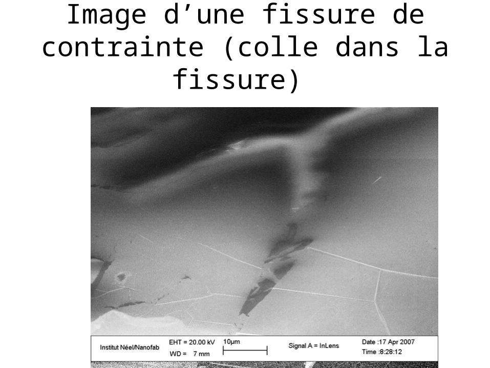
Image d’une fissure de contrainte (colle dans la fissure)
pleats defects
SEM zoom on Pleats defects
Graphene on epi SiC (GaTech U.) :
same kind of pleats
1µm
Effective surface potentialSonde de Kelvin
Scanning Potential Microscopy
Lift height = 5 nm Tip bias = 2V 6 µm Scan
Raman Probing The Raman spectrum of graphite is composed of a strong band at 1582 cm-1, which has been assigned to the in-plane E2g zone centre mode (G band).
Raman Probing The Raman spectrum of graphite is composed of a strong band at 1582 cm-1, which has been assigned to the in-plane E2g zone centre mode (G band).
Raman Probing The Raman spectrum of graphite is composed of a strong band at 1582 cm-1, which has been assigned to the in-plane E2g zone centre mode (G band).
G-band clearly downshifts with increasing n
Gupta et al. Nano Lett., Vol. 6, No. 12, p.2668 2006A. C. Ferrari, et al. Phys. Rev. Lett. 97, 187401 (2006).
MicroRaman spectra are collected using a X100 objective with a spot size of 1m using 514.5 nm excitation under ambient conditions at low laser power (<1mW).
• Marche monocouche
• Colle ? Bulle
AFM sur Zone Raman Monocouche (2)
AFM sur Zone Raman Monocouche (2)
1 µm
Fissure de contrainte ?
2 µm
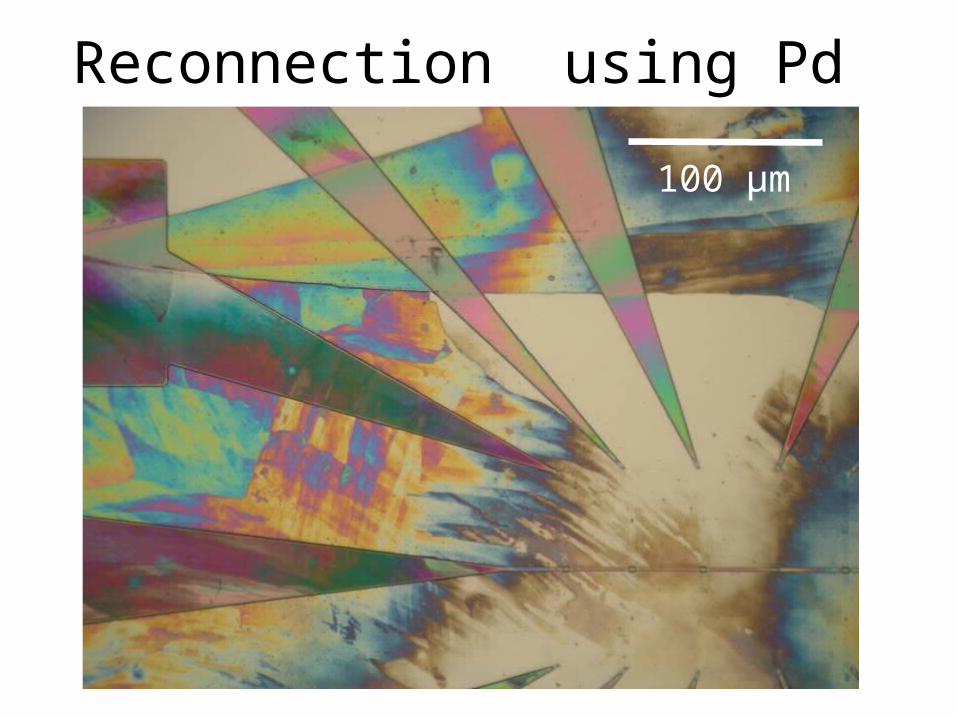
Reconnection using Pd
100 µm
Contacts Pd/Graphene
5 µm
Conclusion :
Reverse exfoliation make possible the realization of flat graphene sheets