j ourna l homepage: www.e lsev ie r .com/ locate /mr
A methodologic project to characterize and model COTS component reliability
A. Durier a,b,⁎, A. Bensoussan a,c, M. Zerarka a, C. Ghfiri a, A. Boyer d, H. Frémont e
a Institut de Recherche Technologique Saint Exupery, 31432 Toulouse, Franceb Continental Automotive France, 31036 Toulouse, Francec Thales Alenia Space France, 31037 Toulouse, Franced LAAS-CNRS France, 31031 Toulouse, Francee Laboratoire de l'Intégration du Matériau au Système, 33405 Talence, France
⁎ Corresponding author at: Institut de Recherche TechnToulouse, France.
Please cite this article as: A. Durier, et al., A mReliability (2015), http://dx.doi.org/10.101
a b s t r a c t
a r t i c l e i n f o
Article history:Received 26 May 2015Received in revised form 22 June 2015Accepted 30 June 2015Available online xxxx
Keywords:COTS reliabilityReliability characterizationEMC IC modelingImmunity to natural radiation modelingComponent Assembly modelingSoldered join reliability characterization
The industries of transportation as the space industry are facedwith a strong global economic competitionwhichsets economic constraints on the cost of the functions. The use of COTS (Commercial Off-The-Shelf) componentsin embedded systems ismore andmore necessary to shorten the development cycles and reducemanufacturingcosts. The application of electronic components comes overwhelmingly from public sectors whose requirementis to provide, in short development cycles, technological innovations including risk and costmitigation. These de-velopment cycles must incorporate the specific constraints of embedded systems in terms of reliability, depend-ability, and availability, held in harsh environment and life.Due to the low volume of components supplying the market of embedded systems, component manufacturersare unlikely to provide information necessary to supporting folders for certification or qualification. It is thereforenecessary for the Space, Aeronautics and Automotive industries to characterize the performance and robustnessof these COTS components in the operational and environmental conditions of their applications.This paper presents the objectives and main challenges of a sponsored project dedicated to characterize andmodel COTS reliability.
The Electronics Robustness Project managed by TechnologyResearch Institute (IRT) Saint-Exupery has two main objectives:
• Develop a generic platform for COTS' reliability characterization,• Develop modeling tools for COTS' reliability prediction.To achieve these objectives, the project is divided in 4 work-packages(WPs):
• WP1: Characterization/modeling of reliability and life time expectancy,• WP2: Characterization/modeling of immunity to natural radiations,• WP3: Characterization/modeling of EMC behavior (emission, immuni-ty, signal integrity) and immunity to transients,
• WP4: Characterization/modeling of themechanical assembly (packageon substrate).
For the next 3 years, chosen technologies for study are GaN (galliumnitride) commercial technologies for power switching and a 28 nmFDSOI (Fully Depleted Silicon On Insulator) digital technology.
ologique Saint Exupery, 31432
ethodologic project to cha6/j.microrel.2015.06.140
2. Characterization/modeling of reliability and life time expectancy
The most used mathematical approach in forecasting reliability isbased on the Arrhenius law. While in chemistry, transition state theoryaimed to explain the kinetics of reaction for elementary chemical reac-tions. This theory postulates the existence of a kind of chemical equilib-rium, the near-equilibrium between reactants and activated transitioncomplex as illustrated by Fig. 1.
This theory allows to use the Free Gibbs Energy to calculate the prob-ability of transition for a chemical reaction characterized by its rate ofreaction proportional to the energy height of the transition state be-tween the initial state and the intermediate state namedΔG‡ or Ea. Sim-ilarly to this physical law, electronic reliability prediction presented inpaper [1] will postulate that the initial state of the component is corre-sponding to healthy devices considered electrically “good” within itsspecification limits and the final state of the component correspondsto out of specification limit devices then considered as failed.
This theory allows determining the time to failure (TTF) of a compo-nent based on the activation energy Ea expressed in eV and the temper-ature T expressed in Kelvin according Arrhenius law:
TTF ¼ A � exp Ea=kTð Þ ð1Þ
where A is a frequency factor and k is the Boltzmann's constant.
racterize and model COTS component reliability, Microelectronics
2 A. Durier et al. / Microelectronics Reliability xxx (2015) xxx–xxx
From this theory, an extensivemathematicalmodel was constructedwhereas the energy provided by external stresses γ · S acting on thecomponents (e.g., electrical transient, overvoltage, natural radiations)decreases the activation energy necessary for a state change and there-fore acts as a catalyst, accelerating the degradation process. As illustrat-ed by Fig. 2, the new activation energy equals:
Uo ¼ Ea− γ � S: ð2Þ
Applying Eq. (2) to Eq. (1), time to failure becomes:
TTF ¼ A � exp Ea − γ � S=kTð Þ: ð3Þ
This model is known in literature as Boltzmann–Arrhenius–Zhurkov(BAZ) model [2,3].
Therefore, it becomes necessary to characterize Ea and γ · S for eachfunctional and physical parameter (e.g., value of leakage current) repre-sentative of the initial state of the component. As these settings aremul-tiple and the stresses are combined, the development of a plan ofexperience becomes essential. A theoretical identification of the param-eters affecting the robustness of the component must be realized first.Experience plan will promote environmental stress and the operatingconditions to be applied to reveal this influence: High Temperature Op-erating Life (HTOL), Low Temperature Operating Life (LTOL), thermalshock, Electrical Over Stress, short circuit, Avalanche Breakdown….
To characterize Ea and γ · S, DC/AC electrical parameters will be de-termined from MIL standard measurements in a temperature range of−55 to +200 °C. It is therefore necessary also to characterize the junc-tion temperatures and hot points by infra-red or electrical method. Theaccelerated aging, representative of equipmentmission profile,will pro-vide time to failure TTF.
Fig. 2. Transition state theory considering a catalyst.
Please cite this article as: A. Durier, et al., A methodologic project to chaReliability (2015), http://dx.doi.org/10.1016/j.microrel.2015.06.140
Finally, a failure analysis by appropriate techniques (electron mi-croscopy, X-ray tomography, optical microscopy to light emission)will establish precisely the component wear out.
The reliability model of COTS components will be consolidated tak-ing into account electrical and thermal operating conditions and thespecific mission profile of final application. The project will establish aFIDES compatible guide to design COTS-based systems.
3. Characterization/modeling of immunity to natural radiations
Wide bandgap semiconductor presents a significant technologicalbreakthrough compared to silicon semiconductor. Main benefits ofthese materials are higher junction temperature, higher critical electri-cal field allowing higher breakdown voltages, lower thermal resistivity,excellent reverse recovery inducing lower switching losses andallowing higher switching frequencies. GaN transistors foreseen inhigh power switching application (DC-DC converters, boosters, …)shows better performance than Si or SiC transistors in terms of ratio“On resistance value/voltage breakdown”, which is the most importantfigure of merit for a power switch. Fig. 3 illustrates the efficiency ratiocomparison between Si and GaN for power switching.
This WP aims to characterize the sensitivity to cosmic/atmosphericradiation of GaN Normally OFF commercial technologies used in lowfrequency switching power conversion. Characterization will be madefrom the environmental constraints faced by different systems (space,aeronautics and terrestrials). The results of this WP will be used to en-rich reliability models developed in WP1.
This WP will first address SEE (Single Event Effects) as SEB (SingleEvent Burnout). SEGR (Single Event Gate Rupture) are not expected insuch devices with pGaN gate since there is no insulating layers whichcould be the source of failure.
We have proceeded to a detailed physical analysis of manufacturingprocesses of the GaN normally-off commercial used in power conver-sion. Considered GaN transistors were EPC 2019 (200 V/10 A) andGaN Systems GS66508P (650 V/19 A). The cross section analysis asshown by Fig. 4 enables to know about transistor's epitaxy.
A fine analysis wasmade at the level of the active area. This analysisshows that active area (drain to source distance ~7 μm for EPC and~21 μm for GaN Systems transistor) is made of a complex multiple setof AlGaN layers grown on a Si substrate. We have also proceeded tothe identification of the constituentmaterials of the chip aswell as anal-ysis of the assembly of the chip into the package.
This construction analysis has been used to build TCAD (TechnologyComputed Aided Design) transistor model as illustrated by Fig. 5. Mea-surements of the static electrical characteristics allowed calibrating andvalidating this TCAD model.
Immunity to natural radiations will be simulated under TCAD(Sentaurus) in a temperature range of −55 to +200 °C to quantify
Fig. 3. Power conversion efficiency GaN vs Si.
racterize and model COTS component reliability, Microelectronics
Fig. 6. Simulated transients events after heavy ion impact on EPC2019 GaN transistor. (Forinterpretation of the references to color in this figure legend, the reader is referred to theweb version of this article.)
3A. Durier et al. / Microelectronics Reliability xxx (2015) xxx–xxx
the fullness of reactions, locate theoretically sensitive areas and to iden-tify triggermechanisms. Unlike Si MOS transistor, some previous worksregarding RFHEMT [4,5,6] suggest that SEEs into AlGaN/GaNHEMTs aremainly due to displacement damage more than to ionization effects.However, todays TCAD radiation models cannot take into account dis-placement damage, which would be the reason why TCAD tools arenot yet well-suited to these new technologies and finally the studymay become unsuccessful.
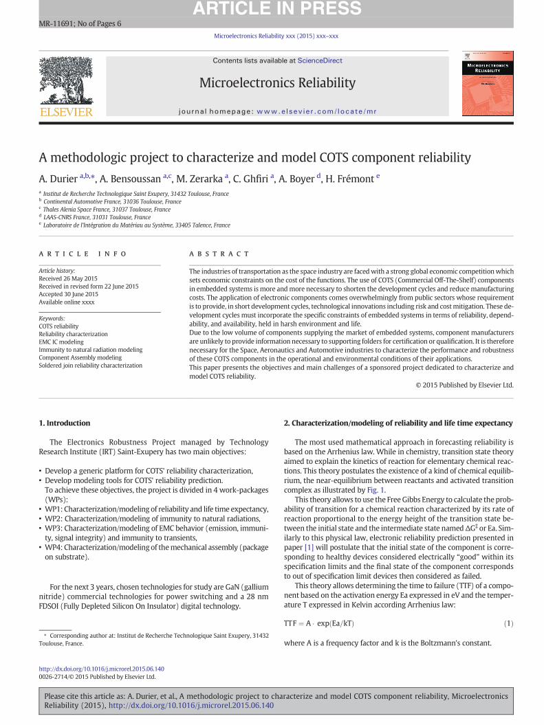
Fig. 6 shows the very first results obtained after a simulationof heavy ion impact. For the same LET (Linear Transfer Energy) of1 pC/μm but two different drain to source voltages VDS, we reproducetwo levels of transients, one at VDS = 200 V with IDSmax N 3 A (redcurve) the other at VDS = 50 V with IDSmax = 1.2 A.
Fig. 7 shows the evolution of electron density along the time. At t0, anElectroMagnetic field is created between the impacts by ionizationpoints. At t1, we observe the beginning of avalanche phenomena. At t2,we observe holes injection near the drain. At t3, we may observe theSEB.
An analysis of sensitivity under laser beam will be therefore imple-mented to assess areas of sensitivity andmodes of failure prior to the ir-radiation under beams of particles (neutrons, protons and heavy ions).
Knowledge of the natural radiation environment for different appli-cations (automotive, aeronautical and space)will then assess the Failurein Time (FIT) for a given application. Electrical characterization aftercampaigns under beams will allow the correlation of the measurewith the modeling developed in the WP1. This WP will lead to enrichthe predictive reliability model defined in WP1, determining the γ · Slinked to natural radiations.
Fig. 5. EPC 2019 GaN transistor TCAD model.
Please cite this article as: A. Durier, et al., A methodologic project to chaReliability (2015), http://dx.doi.org/10.1016/j.microrel.2015.06.140
4. Characterization/modeling of EMCbehavior (emission, immunity,signal integrity) and immunity to transients
One of the embedded electronic industrial problems is to predict therisk of failures and non-compliance EMC of their equipment along theirlifetime. This WP aims therefore to extend the current EMC IEC 62433standards for Integrated Circuits to include the effects of aging and pre-dict average derivatives and the dispersal of their emission and immu-nity levels. Then, it comes to demonstrate that these models allowprediction of the risk of non-compliance at the level of an electronicboard.
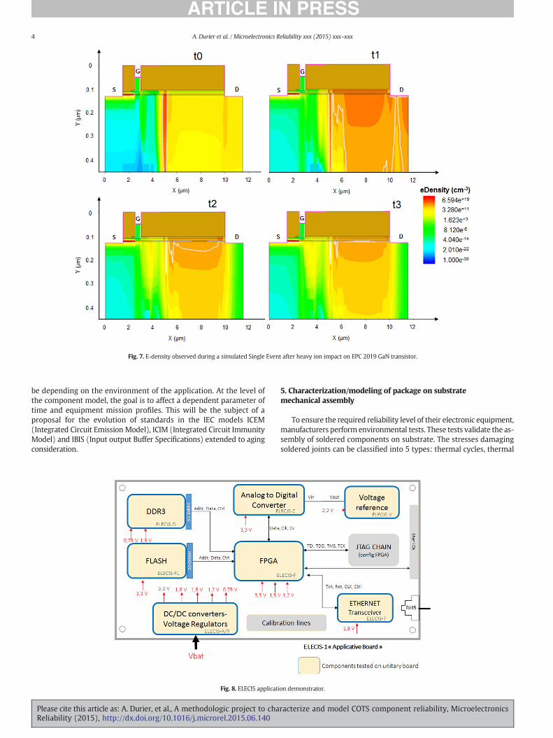
This WP will address proven technologies for functions commonlyused in aeronautical or automotive ECUs. As illustrated by Fig. 8, an ap-plication demonstrator called ELECIS (Electronic board for Long termElectromagnetic Compatibility Issues Simulation) has been designedaround a FPGA addressing different types of memory (flash, MRAM,DDR3), communicating thru an external ETHERNET bus and supportinganalog functions as Analog to Digital Converter (ADC), reference voltageand supplied by linear and switched power supplies.
Table 1 gives the list of components which will be modeled. Tran-sient Voltage Suppressor (TVS) as well as passive elements will be alsomodeled.
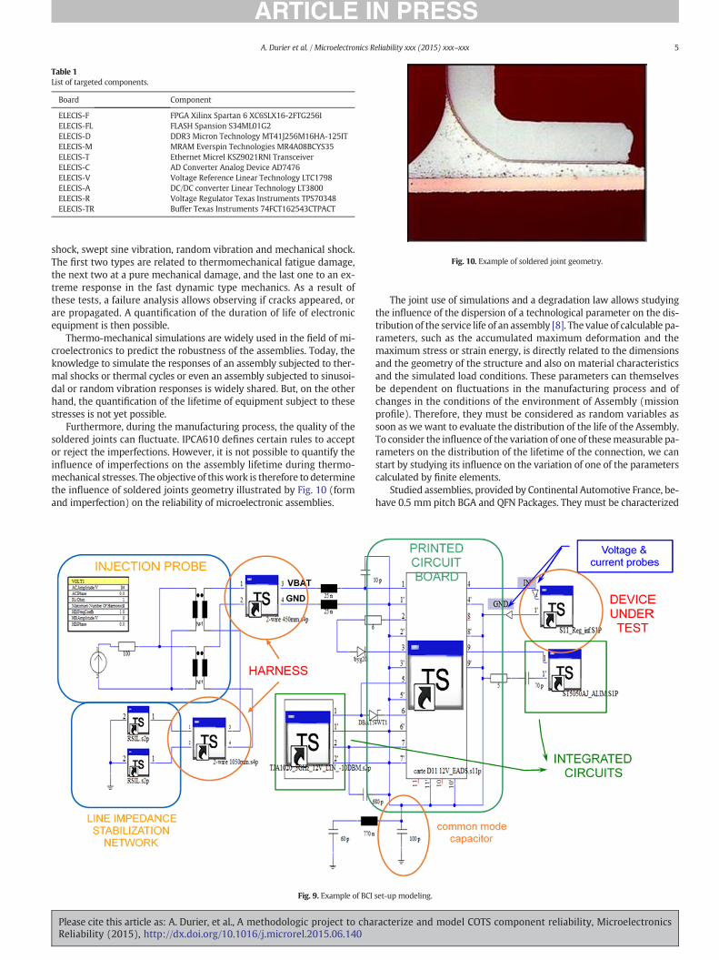
For each component, we will choose the EMC (emission andimmunity) and transient immunity measurement method adapted toextract the component model. A complete ELECIS demonstrator modelwill be established in white box by the association of different active,passive components models as well as the PCB tracks. EMC (emissionand immunity) and transient's immunity normative set-up modelswill be established which will require the creation of cable, antennas,injection probe pulse generator, and ESD gun models. Fig. 9 shows anexample of BCI (Bulk Current Injection) set-up modeling as presentedin the paper [7]. This modeling allows to calculate the equivalent DPI(Direct Power Injection) level obtain at component level during a BCItest.
EMC measurement according CISPR25, DO160 or ISO standard willbe performed on the application demonstrator ELECIS in order to corre-late the model to the measure.
The same measurements and modeling will be conducted on ageddemonstrators. The aging of components and the demonstrator will
racterize and model COTS component reliability, Microelectronics
Fig. 7. E-density observed during a simulated Single Event after heavy ion impact on EPC 2019 GaN transistor.
4 A. Durier et al. / Microelectronics Reliability xxx (2015) xxx–xxx
be depending on the environment of the application. At the level ofthe component model, the goal is to affect a dependent parameter oftime and equipment mission profiles. This will be the subject of aproposal for the evolution of standards in the IEC models ICEM(Integrated Circuit Emission Model), ICIM (Integrated Circuit ImmunityModel) and IBIS (Input output Buffer Specifications) extended to agingconsideration.
Fig. 8. ELECIS applicati
Please cite this article as: A. Durier, et al., A methodologic project to chaReliability (2015), http://dx.doi.org/10.1016/j.microrel.2015.06.140
5. Characterization/modeling of package on substratemechanical assembly
To ensure the required reliability level of their electronic equipment,manufacturers perform environmental tests. These tests validate the as-sembly of soldered components on substrate. The stresses damagingsoldered joints can be classified into 5 types: thermal cycles, thermal
on demonstrator.
racterize and model COTS component reliability, Microelectronics
ELECIS-F FPGA Xilinx Spartan 6 XC6SLX16-2FTG256IELECIS-FL FLASH Spansion S34ML01G2ELECIS-D DDR3 Micron Technology MT41J256M16HA-125ITELECIS-M MRAM Everspin Technologies MR4A08BCYS35ELECIS-T Ethernet Micrel KSZ9021RNI TransceiverELECIS-C AD Converter Analog Device AD7476ELECIS-V Voltage Reference Linear Technology LTC1798ELECIS-A DC/DC converter Linear Technology LT3800ELECIS-R Voltage Regulator Texas Instruments TPS70348ELECIS-TR Buffer Texas Instruments 74FCT162543CTPACT
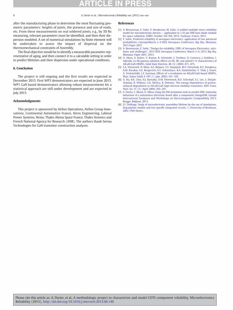
Fig. 10. Example of soldered joint geometry.
5A. Durier et al. / Microelectronics Reliability xxx (2015) xxx–xxx
shock, swept sine vibration, random vibration and mechanical shock.The first two types are related to thermomechanical fatigue damage,the next two at a pure mechanical damage, and the last one to an ex-treme response in the fast dynamic type mechanics. As a result ofthese tests, a failure analysis allows observing if cracks appeared, orare propagated. A quantification of the duration of life of electronicequipment is then possible.
Thermo-mechanical simulations are widely used in the field of mi-croelectronics to predict the robustness of the assemblies. Today, theknowledge to simulate the responses of an assembly subjected to ther-mal shocks or thermal cycles or even an assembly subjected to sinusoi-dal or random vibration responses is widely shared. But, on the otherhand, the quantification of the lifetime of equipment subject to thesestresses is not yet possible.
Furthermore, during the manufacturing process, the quality of thesoldered joints can fluctuate. IPCA610 defines certain rules to acceptor reject the imperfections. However, it is not possible to quantify theinfluence of imperfections on the assembly lifetime during thermo-mechanical stresses. The objective of thiswork is therefore to determinethe influence of soldered joints geometry illustrated by Fig. 10 (formand imperfection) on the reliability of microelectronic assemblies.
Fig. 9. Example of BCI
Please cite this article as: A. Durier, et al., A methodologic project to chaReliability (2015), http://dx.doi.org/10.1016/j.microrel.2015.06.140
The joint use of simulations and a degradation law allows studyingthe influence of the dispersion of a technological parameter on the dis-tribution of the service life of an assembly [8]. The value of calculable pa-rameters, such as the accumulated maximum deformation and themaximum stress or strain energy, is directly related to the dimensionsand the geometry of the structure and also on material characteristicsand the simulated load conditions. These parameters can themselvesbe dependent on fluctuations in the manufacturing process and ofchanges in the conditions of the environment of Assembly (missionprofile). Therefore, they must be considered as random variables assoon as we want to evaluate the distribution of the life of the Assembly.To consider the influence of the variation of one of thesemeasurable pa-rameters on the distribution of the lifetime of the connection, we canstart by studying its influence on the variation of one of the parameterscalculated by finite elements.
Studied assemblies, provided by Continental Automotive France, be-have 0.5 mm pitch BGA and QFN Packages. They must be characterized
set-up modeling.
racterize and model COTS component reliability, Microelectronics
6 A. Durier et al. / Microelectronics Reliability xxx (2015) xxx–xxx
after the manufacturing phase to determine the most fluctuating geo-metric parameters: heights of joints, the presence and size of voids,etc. From these measurements on real soldered joints, e.g., by 3D Rxmeasuring, relevant parameters must be identified, and then their dis-persion modeled. A set of numerical simulations by finite element willbe undertaken to assess the impact of dispersal on thethermomechanical constraints of Assembly.
The final objectivewould be to identify ameasurable parameter rep-resentative of aging, and then connect it to a calculable setting in orderto predict lifetimes and their dispersion under operational conditions.
6. Conclusion
The project is still ongoing and the first results are expected inDecember 2015. First WP3 demonstrators are expected in June 2015.WP1 GaN based demonstrators allowing robust measurements for astatistical approach are still under development and are expected inJuly 2015.
Acknowledgments
This project is sponsored by Airbus Operations, Airbus Group Inno-vations, Continental Automotive France, Hirex Engineering, LabinalPower Systems, Nexio, Thales Alenia Space France, Thales Avionics andFrench National Agency for Research (ANR). The authors thank SermaTechnologies for GaN transistor construction analyses.
Please cite this article as: A. Durier, et al., A methodologic project to chaReliability (2015), http://dx.doi.org/10.1016/j.microrel.2015.06.140
References
[1] A. Bensoussan, E. Suhir, P. Henderson, M. Zahir, A unified multiple stress reliabilitymodel for microelectronic devices — application to 1.55 μm DFB laser diode modulefor space validation, ESREF, October 5th–9th, 2015, Toulouse, France. 2015.
[2] E. Suhir, Predicted reliability of aerospace electronics: application of two advancedprobabilistic conceptsMarch 2–9 IEEE Aerospace Conference, Big Sky, Montana,2013 Paper 2037.
[3] A. Bensoussan, E. Suhir, “Design-for-reliability (DfR) of Aerospace Electronics: attri-butes and challenges”, 2013 IEEE Aerospace Conference, March 2–9, 2013, Big Sky,Montana, Paper 2057, 2013.
[4] O. Aktas, A. Kuliev, V. Kumar, R. Schwindt, S. Toshkov, D. Costescu, J. Stubbins, I.Adesida, Co-60 gamma radiation effects on DC, RF, and pulsed I–V characteristics ofAlGaN/GaN HEMTs, Solid State Electron. 48 (3) (2004) 471–475.
[5] S.A. Vitusevich, N. Klein, A.E. Belyaev, S.V. Danylyuk, M.V. Petrychuk, R.V. Konakova,A.M. Kurakin, A.E. Rengevich, A.Y. Avksentyev, B.A. Danilchenko, V. Tilak, J. Smart,A. Vertiatchikh, L.F. Eastman, Effects of γ-irradiation on AlGaN/GaN-based HEMTs,Phys. Status Solidi A 195 (1) (Jan. 2003) 101–105.
[6] X. Hu, B.K. Choi, H.J. Barnaby, D.M. Fleetwood, R.D. Schrimpf, S.C. Lee, S. Shojah-Ardalan, R. Wilkins, U.K. Mishra, R. Dettmer, The energy dependence of proton-induced degradation in AlGaN/GaN high electron mobility transistors, IEEE Trans.Nucl. Sci. 51 (2) (April 2004) 293–297.
[7] A. Durier, C. Marot, O. Alilou, Using the EM simulation tools to predict EMC immunitybehaviour of a automotive electronic board after a component changeEMC EuropeInternational Symposia and Workshops on Electromagnetic Compatibility 2013,Brugge, Belgium, 2013.
[8] J.Y. Delétage, Study of microelectronic assemblies lifetime by the use of simulations,degradation models and test specific integrated circuits, 1, University of Bordeaux,2003 (PhD thesis).
racterize and model COTS component reliability, Microelectronics