Abstract— This article presents design techniques tofacilitate the use of the driving point impedance (Z11) ofone-port transformer-coupled resonators as wideband loadsof millimeter-wave amplifier stages for a 28-GHz receiverfront end. While the use of both the Z11 of a one-port andthe transimpedance (Z21) of a two-port coupled resonator isconsidered to achieve a wideband response, it is shown thatunder conditions of low magnetic coupling and constrainednetwork quality factor, the use of Z11 can result in a highergain–bandwidth product of low-noise amplifier (LNA) amplifierstages. The effect of the complex zero in the Z11 response onthe in-band gain ripple is shown to be alleviated merely bylowering the quality factor of the transformer’s secondary coil;this strongly motivates the use of compact, nested-inductortransformer layouts. Implemented in a 65-nm CMOS process, athree-stage LNA (with Z11 wideband loads in two stages) achievesa 24.4–32.3-GHz bandwidth (27.9 % fractional bandwidth),a peak S21 of 24.4 dB (20.4 dB), a minimum noise figure (NF)of 4 dB (4.6 dB), and an input-referred P1dB of −23 dBm(−22 dBm) while consuming 22-mW (9.9 mW) power from a1.1-V (0.85 V) supply. The use of compact transformers limits theLNA’s footprint to only 0.12 mm2. A 26.5–32.5-GHz quadraturereceiver prototype employing the LNA achieves a 29.5-dB peakconversion gain, a 5.3-dB minimum NF, and a −26-dBm input-referred P1dB while consuming 33 mW from a 1.1-V supply.
PHASED-ARRAY transceivers [1]–[3] are required toovercome path loss and realize advanced multiple-input–
multiple-output (MIMO) communication in emerging 5G net-works in the 28-/38-GHz bands [4]. Since antenna arrayswith high element count are needed, it is important forthe transceiver circuits to be compact, scalable and energy-efficient. In particular, wideband low-noise amplifiers (LNAs)
Manuscript received December 6, 2019; revised January 31, 2020; acceptedFebruary 29, 2020. This work was supported in part by the NationalScience Foundation under Grant EECS-1343324 and Grant CCF-1314876.(Corresponding author: Rahul Singh.)
Rahul Singh was with the Department of Electrical and Computer Engi-neering, Carnegie Mellon University, Pittsburgh, PA 15217 USA. He isnow with Qualcomm Inc., San Diego, CA 92121 USA (e-mail: [email protected]).
Susnata Mondal and Jeyanandh Paramesh are with the Department of Elec-trical and Computer Engineering, Carnegie Mellon University, Pittsburgh, PA15217 USA (e-mail: [email protected]; [email protected]).
Color versions of one or more of the figures in this article are availableonline at http://ieeexplore.ieee.org.
Digital Object Identifier 10.1109/TMTT.2020.2985676
Fig. 1. Comparison of the transimpedance frequency response of atwo-port transformer-coupled resonator (Z21) with the frequency response ofa ripple-compensated one-port coupled-resonator (Z11) with (Q1 = 0.5Q2)and without (Q2 = Q1) compensation. L = 200 pH, C = 140.7 fF, k = 0.18,and Q1 = 10. Q1 and Q2 are the circuit quality factors of the two LC tanks.
that can cover contiguous and/or widely separated narrow-band channels of a diverse spectrum [3] with low costand small die area are of high interest, especially inthe 60-GHz [5]–[7] and the 28-GHz bands [3], [8], [9].Recently, coupled LC resonators have received wide inter-est in various millimeter-wave (mm-wave) circuits, includingLNAs [3], [8]–[10], wide-tuning voltage-controlled oscillators(VCOs) [11], [12], and power amplifiers (PAs) [13], [14]. Theresonators can be coupled capacitively, inductively (through anexplicit inductor), or magnetically (through a mutual induc-tance), and each result in a fourth-order transfer function.Magnetic coupling is usually preferred since it results in alower ripple for a given bandwidth [6]. Recent mm-waveLNAs in this class exclusively use the transimpedance (Z21) ofweakly coupled transformer-coupled resonators as widebandloads [3], [5], [6].
In this article, design techniques are introduced to enablethe use of the input driving point impedance (Z11) of a one-port coupled resonator as a wideband load. A comparisonof the properties of Z11 and Z21 shows that adopting Z11over Z21 can result in a higher gain–bandwidth (GBW)product if the in-band gain ripple of the Z11 response isadequately tempered. In Section II, it is shown that the Z11gain ripple has a strong dependence on the quality factorof the transformer’s secondary coil, and an effective trans-former design technique is introduced to exploit this property.Fig. 1 compares the ripple-compensated Z11 response of atransformer coupled resonator using the proposed technique
This article has been accepted for inclusion in a future issue of this journal. Content is final as presented, with the exception of pagination.
2 IEEE TRANSACTIONS ON MICROWAVE THEORY AND TECHNIQUES
Fig. 2. Comparison of recently published mm-wave CMOS LNAs(<45 GHz).
with the Z21 response—the increase in the GBW product fora similar in-band ripple is evident. A complete receiver usinga wideband LNA design based on such ripple-compensatedZ11 wideband loads is described in Section III. The char-acterization results of the 65-nm CMOS prototype are pre-sented in Section IV. Fig. 2 compares the LNA figure ofmerit1 (FOM) [6] of the recently reported wideband CMOSLNAs [8], [15]–[28] (only LNAs operating below 45 GHzare considered). The proposed design achieves high FOM anda compact LNA footprint due to the use of nested-inductortransformer layouts. Notably, only [17], implemented in 40-nmCMOS and using spatially offset inductor layouts, achievescomparable FOM but occupies twice the active area.
II. TRANSFORMER COUPLED-RESONATOR
WIDEBAND LOADS
A. Coupled-Resonator Analysis
Consider the simplified model of a transformer-coupledresonator, as shown in Fig. 1. Here, the loss of the resonator ismodeled using resistances in series with the inductances andcapacitances. The following definitions are made:
k = M
L1 L2, ω1 = 1√
L1C1, ω2 = 1√
L2C2, ξ =
�ω1
ω2
�2.
(1)
After discarding the high-frequency zeros, the driving pointimpedance (Z11) and the transimpedance (Z21) can be writtenin the pole-zero form as [10]2
Z21(s) = sM�s2
ω2p1
+ sQ p1ωp1
+ 1��
s2
ω2p2
+ sQ p2ωp2
+ 1�
Z11(s) =sL1
�s2
ω2z2
+ sQz2ωz2
+ 1�
�s2
ω2p1
+ sQ p1ωp1
+ 1��
s2
ω2p2
+ sQ p2ωp2
+ 1� . (2)
1The LNA FOM adopted for comparison has been widely used both inthe past for narrowband LNAs [29], [30] (where the effect of LNA BWis not considered) as well as in the latest mm-wave research on widebandLNAs [6], [7] (where the effect of LNA BW is included in the FOMcalculation).
2The effect of interwinding capacitance Cc is omitted here to simplify theanalysis. The effect of Cc on the coupled resonator’s frequency response isanalyzed rigorously in [5] and [12].
Fig. 3. Definitions of magnitude response parameters.
In (2), the low-frequency zero (ωz1) of Z11 is replaced by azero at the origin. The quality factors of the complex-conjugatepoles can be obtained by a circuit analysis based on successiveseries–parallel transformations and can be approximated by thefollowing expressions:
Q p1 = 2�
Q1 Q2
Q1 + Q2
�√1 + k
Q p2 = 2�
Q1 Q2
Q1 + Q2
�√1 − k (3)
where Q1 and Q2 are the circuit quality factors of the LCtanks. The location of the poles can be shown to be [11], [12]
ωp1,p2 = ω2
��1 + ξ ±
�(1 + ξ)2 − 4ξ(1 − k2)
2(1 − k2)
�ξ=1−→ ωp1,p2 = ω2√
1 ± k. (4)
From (2), it is seen that Z11 has an additionalcomplex-conjugate zero pair, whose frequency and qualityfactor can be derived as
ωz2 = ω2√1 − k2
, Qz2 = Q1 Q2√
1 − k2
Q1 + k2 Q2≈ Q2(low-k). (5)
Fig. 3 shows the typical frequency response of magnitudes ofZ11 and Z21 of a transformer-coupled resonator. The peak gainmagnitudes G1 and G3 can be obtained by evaluating (2) at thepole frequencies. Assuming ξ = 1 for simplicity, the followingexpressions are obtained:
G1,Z11 = Q p1ωp1 L1
�1+k
2
��1+ 1 − k
k2Q2z2
�1/2�1+ 1 − k2
4k2Q2p2
�−1/2
G3,Z11 = Q p2ωp2 L1
�1−k
2
��1+ 1 + k
k2Q2z2
�1/2�1+ 1 − k2
4k2Q2p1
�−1/2
(6)
G1,Z21 = Q p1ωp1 M�
1 + k
2k
��1 + 1 − k2
4k2 Q2p2
�−1/2
G3,Z21 = Q p2ωp2 M�
1 − k
2k
��1+ 1 − k2
4k2 Q2p1
�−1/2
. (7)
Authorized licensed use limited to: Carnegie Mellon Libraries. Downloaded on June 09,2020 at 15:13:00 UTC from IEEE Xplore. Restrictions apply.
This article has been accepted for inclusion in a future issue of this journal. Content is final as presented, with the exception of pagination.
SINGH et al.: mm-WAVE RECEIVER USING WIDEBAND LOW-NOISE AMPLIFIER WITH ONE-PORT COUPLED RESONATOR LOADS 3
Fig. 4. (a) Primary side Q swept, Q2 = 7.8. (b) Secondary side Q swept,Q1 = 12.7. The dashed and solid lines represent the magnitude responseparameters of Z21 and Z11, respectively.
Similarly, the magnitude of Z11 at the zero frequency canbe written as
G2,Z11=
ωp2 L1
1−k2
�Qz2
��1+ 1 − k
k2 Q2p1
�−1/2�1+ 1 + k
k2 Q2p2
�−1/2
.
(8)
B. Effect of Quality Factor on GBW Product
In order to achieve high GBW product, the magnituderesponses of Z11 and/or Z21 must have three attributes: 1) wide−3-dB bandwidth; 2) high gain; and 3) sufficiently lowripple R. From (4), it is seen that wide bandwidth can beachieved by exploiting the pole-splitting action of a coupledresonator [6] to achieve sufficiently large separation betweenthe poles of the fourth-order system. In order to achievehigh gain, the magnitude peaks of Z11 and Z21 (G1 andG3 in Fig. 3), which occur roughly at the pole frequenciesf p1 and f p2, must be large. As shown by (6) and (7), thesegains increase with the pole quality factors Q p1 and Q p2,which in turn depend on the quality factors of both primary-and secondary-side resonators, as shown by (3). Flatness ofthe frequency response within the passband is determinedby the difference between gain magnitude G1 (or G3) andthe magnitude G2 between the two poles, identified as thegain ripple R in Fig. 3. For both Z11 and Z21, G2 can beconveniently approximated as the magnitude at the complexzero frequency ωz2 of Z11. Note that the Z21 response does notcontain a complex zero and its G2 magnitude is determinedby the gain roll-off responses of the two complex pole pairs.From (4) and (5), it can be observed that Z11’s complex zeroωz2 lies between the two complex poles and hence stronglydetermines G2. In particular, the complex zero causes a notch,whose depth increases as the quality factor Qz2 increases.
The earlier observations are illustrated by an examplein Fig. 4, where the coupled resonator of Fig. 1 is simulatedwith L1 = L2 = 200 pH, k = 0.15, and C1 = C2 =155 fF. The dependences of the gains G1–G3 on Q1 and Q2are plotted in Fig. 4(a) and (b), respectively. Two importantconclusions are validated.
1) From (5), it is observed that for low values of k, Qz2 ismore strongly affected by the secondary-side quality
Fig. 5. (a) Peak gain, (b) bandwidth, and (c) GBW for a ripple specificationof R = 4 dB. Solid lines represent Z11, and dashed lines represent Z21.
factor Q2 than the primary-side quality factor Q1.Consequently, Fig. 4(a) and (b) reveals that that Z11’sG2[see (8)], which determines the notch depth, variesstrongly with the secondary-side Q2 but is relativelyinsensitive to the primary-side Q1.
2) It is also observed that the gain magnitudes G1 and G3of Z11 show a stronger dependence on Q1 than Q2.This contrasts with the behavior of Z21 pole gains G1and G3, which shows an equally strong dependence onboth Q1 and Q2. This observation is validated by (6),where we see that when compared to Z21 expressionsin (7), the expressions for Z11’s G1 and G3 contain anadditional term dependent on Qz2 (and hence on Q2),which tempers the otherwise strong dependence of thesepole magnitudes on Q2.
The above mentioned two points lead to a key observationthat is exploited in our LNA prototype presented in Section III;the gain ripple in Z11’s response can be controlled by usingmoderate values of Q2 while maintaining sufficiently largevalues of G1 and G3. In other words, even though the qualityfactor of the secondary coil is reduced to compensate for theZ11 ripple, the impact on Z11’s GBW is limited.
C. Ripple-Compensated Z11 Versus Z21
Given a ripple specification R, the GBW of Z11 can be madelarger than that of Z21. This is because ripple compensationby reducing Q2 still results in high values of G1 and G3,and outside the passband, Z21 has steeper stopband skirts(see Fig. 1) when compared to Z11 which lowers its −3-dBbandwidth. The much steeper upper stopband slope of Z21,when compared to Z11, is due to the absence of a complexzero between the poles. Using the Bode plots, it can bededuced that the Z11 response has stopbands that roll off at−20 dB/decade (the upper stopband slope is sum of +20,−40, +40, and −40 dB/decade due to ωz1, ωp1, ωz2, and ωp2,respectively). On the other hand, the Z21 response will have a−20-dB/decade slope in the lower stopband (due to the zero)and a −60-dB/decade slope in the upper stopband (sum of+20, −40, and −40 dB/decade due to zero at the origin, ωp1,and ωp2, respectively).
Fig. 5 shows the effect of reducing Q2 on the GBW andthe peak gains for Z11 and Z21 for different values of k.
Authorized licensed use limited to: Carnegie Mellon Libraries. Downloaded on June 09,2020 at 15:13:00 UTC from IEEE Xplore. Restrictions apply.
This article has been accepted for inclusion in a future issue of this journal. Content is final as presented, with the exception of pagination.
4 IEEE TRANSACTIONS ON MICROWAVE THEORY AND TECHNIQUES
Fig. 6. (a) Z11 and Z21 magnitude response with R = 4 dB, where L1 =L2 = 200 pH, k = 0.2, and C1 = C2 = 155 fF. (b) Magnitude response withunequal resonant frequencies (ξ = 1.06), where C1 = 150 fF, C2 = 160 fF,and Q1 = 12.7, to equalize gain peaks G1 and G3 in the Z11 response.
A ripple specification R = 4 dB is chosen in this example,which imposes a maximum value of Q2 beyond which asingle concurrent band can no longer be assumed. Note thatthis definition is somewhat arbitrary and is assumed here forillustrative purposes, and the validity of the analysis belowremains unaltered by choosing a different specification for theripple constraint. In these simulations, L1 = L2 = 200 pH,k = 0.2, and C1 = C2 = 155 fF. The primary-side qualityfactor is set to Q1 = 12.7, which is a reasonable valueat 28 GHz considering the losses of both the inductor andcapacitor. It is clear that for different values of k, higher peakgain, bandwidth, and GBW can be consistently achieved withZ11 when compared with Z21. Fig. 6(a) plots the magnituderesponse of Z11 and Z21, given the 4-dB ripple constraint,for a k of 0.2. It is observed that the maximum GBWsof 1910 and 1607 GHz are achieved for Z11 and Z21 atQ2 = 5.2 and 9.5, respectively. A further advantage of usingZ11 is that the zero frequency ωz2 can be adjusted to achieveequal gain peaks G1 and G2. By choosing unequal tankresonant frequencies (ξ �= 1) through unequal primary- andsecondary-side capacitances, ωz2 in the Z11 response can bepositioned either close to ωp1 (ξ > 1) or close to ωp2 (ξ < 1).An example is shown in Fig. 6(b), where ξ is set to 1.06 toequalize the Z11 gain peaks. The Z21 response lacks a complexzero and hence lacks this responsiveness to ξ .
For designs that use Z11, certain disadvantages should benoted at this juncture. Here, the transconductor and the loadcircuits are both connected to the primary side of the coupledresonator, and therefore, their capacitances appear in parallelwith the primary-side inductor. This limits the budget allowedfor an external (possibly tunable) capacitance that is typicallynecessary to achieve design margin and tunability. On the otherhand, in designs that use Z21, the transconductor and loadcircuit capacitances appear across that primary and secondarysides, respectively. Therefore, a higher budget is available forthe insertion of explicit tuning capacitors on each side. Theability to separate the transconductor and load capacitancescan be very beneficial in applications where these capaci-tances are typically large, for example, the driver stages ofa PA [13], [14]. However, in an mm-wave LNA amplifieroperating around 28 GHz, which is the focus of this article,
Fig. 7. Cascaded gain stages using (a) Z11 and (b) Z21 wideband loads.
these capacitances are much smaller, and a Z11 wideband loadwith tunable capacitors is as easily realized as a Z21 load.In designs using Z21, the secondary inductor can be used tobias the succeeding stage; however, ac-coupling capacitors andbias resistors are necessary when using a Z11 wideband load.Finally, while both Z11 and Z21 can serve as wideband loadsin both single-ended and differential implementations, a Z21load can also conveniently interface between a single-endedfirst stage and succeeding differential stages [3], [8], [9], [17].
D. Stagger-Tuned Cascaded Gain Stages
To simultaneously achieve high gain and large fractionalbandwidth at mm-wave frequencies, gain stages with low-k coupled-resonator loads should be cascaded and stagger-tuned such that higher ripple (often greater than 3 dB) canbe tolerated in each stage [15]. This is illustrated using anexample in Fig. 7 where two stagger-tuned Z21 and Z11responses of two cascaded stages are compared. The GBWadvantage of Z11 is again clearly evident; the overall Z11response achieves a bandwidth nearly twice that of the Z21response while achieving similar peak gains. It should benoted that since Z21 has steeper skirts in the transition band,it exhibits higher group delay in the passband. However, it wasobserved that by stagger-tuning stages, it is possible to obtaina reasonably flat group delay profile in the passband with bothZ11 and Z21 wideband loads.
III. WIDEBAND RECEIVER DESIGN
The previously discussed techniques were applied to designa wideband LNA that was used in a quadrature receiver frontend. Fig. 8 shows the die photograph and the block diagramof the receiver, designed in a 65-nm CMOS technology.
A. Wideband Low-Noise Amplifier
The proposed wideband LNA design employs three gainstages, as shown in Fig. 9(a). The first stage comprises twoinductively generated common-source (CS) legs—M1 and M2,
Authorized licensed use limited to: Carnegie Mellon Libraries. Downloaded on June 09,2020 at 15:13:00 UTC from IEEE Xplore. Restrictions apply.
This article has been accepted for inclusion in a future issue of this journal. Content is final as presented, with the exception of pagination.
SINGH et al.: mm-WAVE RECEIVER USING WIDEBAND LOW-NOISE AMPLIFIER WITH ONE-PORT COUPLED RESONATOR LOADS 5
Fig. 8. (a) Die photograph and (b) block diagram of the receiver chipin 65-nm CMOS.
Fig. 9. (a) Circuit schematic and (b) layout floorplan of the three-stage LNA.All transistors are of minimum length (60 nm).
degenerated by source inductors L P2 and LS2. In contrast toconventional inductive degeneration, weak coupling is intro-duced between the two inductors (k ∼ 0.2), laid out in nestedconfiguration to save area. The two CS legs are designedto be symmetrical with identical transistor sizes (24 μm)and degenerating inductances (142 pH). To avoid the noisepenalty, a cascode transistor was not used. The first stage
Fig. 10. Equivalent circuit model of the input matching network. Note thatin mode 1, Section II only has an “even” mode of operation due to symmetryand reduces to a series-RLC resonant circuit.
employs a coupled-resonator load (XFMR1) comprising anested transformer and a combination of fixed and switchedmetal–oxide–metal (MOM) capacitors in the primary andsecondary ports; design details of nested transformers and theMOM capacitors are described in Section III-C. The secondCS stage comprises two transistors M3 and M4 in parallelwith a simple LC resonator load; this stage serves to correctthe droop in the frequency response of the first stage. Thethird cascode stage (transistors M5 and M6) uses anothercoupled-resonator load (XFMR3) whose frequency responsestaggered-tuned with respect to the first stage to extend theoverall bandwidth. Each of the CS transistors (M1–M5) wasbiased through a digitally controlled current DAC, therebyallowing independent control of the parallel CS branches instages 1 and 2. The design of the LNA is typically governedby the need to accommodate large input signals due to thepresence of large interferers. In this design, higher linearityconfigurations can be enabled by turning off parts of the firstand second stages, which facilitates linearity to be traded fornoise and voltage gain. In Mode #1, all transistors are ON,whereas in Mode #2, M1–M3–M4 are ON and M2 is turnedoff. In Mode #3, only M1 and M4 are ON, whereas M2 andM3 are turned off.
The layout floorplan of the LNA is shown in Fig. 9(b).A low-impedance power/ground routing network (usingstacked metal layers) is integrated on top of multiple smallbypass capacitor elements and distributed throughout the lay-out. This approach minimizes the parasitic impedances in theac current loops through the bypass capacitances of each LNAstage and the ground return paths. Transformer layouts withnested inductors (see Section III-C) enable a compact layout(370 μm × 325 μm) and help to shorten the high-frequencyinterconnects.
B. Input Matching
A good input match should be maintained in all operatingmodes. This is ensured by an approach described next withreference to Fig. 10, which shows the equivalent circuit ofthe input matching network. The input network is partitioned
Authorized licensed use limited to: Carnegie Mellon Libraries. Downloaded on June 09,2020 at 15:13:00 UTC from IEEE Xplore. Restrictions apply.
This article has been accepted for inclusion in a future issue of this journal. Content is final as presented, with the exception of pagination.
6 IEEE TRANSACTIONS ON MICROWAVE THEORY AND TECHNIQUES
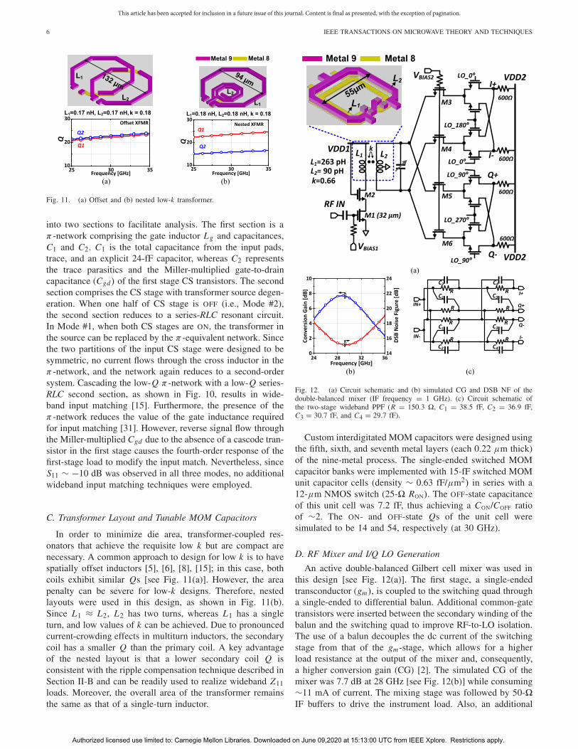
Fig. 11. (a) Offset and (b) nested low-k transformer.
into two sections to facilitate analysis. The first section is aπ-network comprising the gate inductor Lg and capacitances,C1 and C2. C1 is the total capacitance from the input pads,trace, and an explicit 24-fF capacitor, whereas C2 representsthe trace parasitics and the Miller-multiplied gate-to-draincapacitance (Cgd) of the first stage CS transistors. The secondsection comprises the CS stage with transformer source degen-eration. When one half of CS stage is OFF (i.e., Mode #2),the second section reduces to a series-RLC resonant circuit.In Mode #1, when both CS stages are ON, the transformer inthe source can be replaced by the π-equivalent network. Sincethe two partitions of the input CS stage were designed to besymmetric, no current flows through the cross inductor in theπ-network, and the network again reduces to a second-ordersystem. Cascading the low-Q π-network with a low-Q series-RLC second section, as shown in Fig. 10, results in wide-band input matching [15]. Furthermore, the presence of theπ-network reduces the value of the gate inductance requiredfor input matching [31]. However, reverse signal flow throughthe Miller-multiplied Cgd due to the absence of a cascode tran-sistor in the first stage causes the fourth-order response of thefirst-stage load to modify the input match. Nevertheless, sinceS11 ∼ −10 dB was observed in all three modes, no additionalwideband input matching techniques were employed.
C. Transformer Layout and Tunable MOM Capacitors
In order to minimize die area, transformer-coupled res-onators that achieve the requisite low k but are compact arenecessary. A common approach to design for low k is to havespatially offset inductors [5], [6], [8], [15]; in this case, bothcoils exhibit similar Qs [see Fig. 11(a)]. However, the areapenalty can be severe for low-k designs. Therefore, nestedlayouts were used in this design, as shown in Fig. 11(b).Since L1 ≈ L2, L2 has two turns, whereas L1 has a singleturn, and low values of k can be achieved. Due to pronouncedcurrent-crowding effects in multiturn inductors, the secondarycoil has a smaller Q than the primary coil. A key advantageof the nested layout is that a lower secondary coil Q isconsistent with the ripple compensation technique described inSection II-B and can be readily used to realize wideband Z11loads. Moreover, the overall area of the transformer remainsthe same as that of a single-turn inductor.
Fig. 12. (a) Circuit schematic and (b) simulated CG and DSB NF of thedouble-balanced mixer (IF frequency = 1 GHz). (c) Circuit schematic ofthe two-stage wideband PPF (R = 150.3 �, C1 = 38.5 fF, C2 = 36.9 fF,C3 = 30.7 fF, and C4 = 29.7 fF).
Custom interdigitated MOM capacitors were designed usingthe fifth, sixth, and seventh metal layers (each 0.22 μm thick)of the nine-metal process. The single-ended switched MOMcapacitor banks were implemented with 15-fF switched MOMunit capacitor cells (density ∼ 0.63 fF/μm2) in series with a12-μm NMOS switch (25-� RON). The OFF-state capacitanceof this unit cell was 7.2 fF, thus achieving a CON/COFF ratioof ∼2. The ON- and OFF-state Qs of the unit cell weresimulated to be 14 and 54, respectively (at 30 GHz).
D. RF Mixer and I/Q LO Generation
An active double-balanced Gilbert cell mixer was used inthis design [see Fig. 12(a)]. The first stage, a single-endedtransconductor (gm), is coupled to the switching quad througha single-ended to differential balun. Additional common-gatetransistors were inserted between the secondary winding of thebalun and the switching quad to improve RF-to-LO isolation.The use of a balun decouples the dc current of the switchingstage from that of the gm-stage, which allows for a higherload resistance at the output of the mixer and, consequently,a higher conversion gain (CG) [2]. The simulated CG of themixer was 7.7 dB at 28 GHz [see Fig. 12(b)] while consuming∼11 mA of current. The mixing stage was followed by 50-�IF buffers to drive the instrument load. Also, an additional
Authorized licensed use limited to: Carnegie Mellon Libraries. Downloaded on June 09,2020 at 15:13:00 UTC from IEEE Xplore. Restrictions apply.
This article has been accepted for inclusion in a future issue of this journal. Content is final as presented, with the exception of pagination.
SINGH et al.: mm-WAVE RECEIVER USING WIDEBAND LOW-NOISE AMPLIFIER WITH ONE-PORT COUPLED RESONATOR LOADS 7
Fig. 13. LNA measurement results. (a) S21 and S11, (b) variation ofinput-referred 1-dB compression point (iP1dB) with RF frequency, (c) vari-ation of NF with RF frequency, and (d) group delay variation. Simu-lated S21, S11, and NF are shown with dashed lines.
measurement buffer was added at the output of the LNA tofacilitate the standalone characterization.
To simplify the measurement setup, quadrature LO sig-nals for the mixer were generated on-chip using an externalsinusoidal LO signal source. An input balun provided inputmatching and converted the single-ended LO input to a differ-ential signal. A two-stage polyphase filter (PPF) followed thebalun. Layout and parasitic compensation techniques, intro-duced in [32], were followed to improve the PPF’s I/Q accu-racy over a wide bandwidth. The circuit schematic is shownin Fig. 12(c). To compensate for the high signal loss in thetwo-stage PPF, two differential staggered-gain stages followedthe PPF, which ensured a reasonable voltage swing at themixer inputs. The image rejection ratio (IRR) of the LO pathwas simulated to be better than 29 dB between 25 and 32 GHz.
IV. MEASUREMENT RESULTS
A. Breakout LNA Measurements
The LNA was measured in each of its three modesat its nominal 1.1-V VDD and also at reduced VDD of0.95 and 0.85 V. Fig. 13(a) shows the measured and simulatedgain (S21) and input match (S11) of the LNA, respectively. Thesimulated loss of the measurement buffer was deembeddedfrom the measurement. The addition of the measurementbuffer and the presence of a long interconnection betweenthe LNA and the mixer resulted in a slight reduction inbandwidth. Good correlation between the simulations andmeasurements was observed. The in-band input match wasbetter than −7.5 dB.
The linearity of the LNA was characterized through itsinput-referred input compression point (iP1dB). Fig. 13(b)shows the improvement in the linearity performance of the
LNA between Mode #1 and Mode #2. At an RF frequencyof 28 GHz, iP1dB in Mode #1and Mode #2 were mea-sured to be −23 and −21 dBm, respectively. The iP1dB inMode #3 was measured to be −19 dBm; however, this modewas not further characterized as the LNA NF was measuredto be higher than expected (6.2 dB).
The variation of the LNA’s NF with RF frequency isshown in Figs. 13(c). A Noisecom NC346V noise source inconjunction with an Agilent E4440A spectrum analyser wasused for NF measurement. Due to the upper frequency limit ofthe measurement setup, the NF could only be measured up to26.5 GHz. In the low-NF Mode #1 of operation, a minimumNF of 4 dB was observed at 25 GHz. Over 55% reduction inpower was observed in the low-power mode (0.85-V supply).The use of local current mirrors (sharing the LNA VDD)resulted in lowering of transistor biases at reduced supplyvoltages, thereby further reducing the power. The group-delayvariation in Mode #1 was measured to be 73 ± 13 ps over the−3-dB bandwidth, as shown in Fig. 13(d).
B. Comparison With LNA State of the Art
A summary of the LNA performance and benchmarkingagainst similar work is provided in Table I. The LNAdemonstrates a best-case FOM1 [6], [7], [33], [34] of 12.94dB, highest among similar designs, while occupying thesmallest area. FOM1, expressed in dB, adds the impact of LNAbandwidth to the FOM in [29] and [30]. To include the effectof linearity, FOM2 can be used [17]. Unlike FOM1, FOM2 isnot expressed in dB to avoid negative values. The definitionsof FOM1 and FOM2 are noted in Table I. A few LNAsreported in Table II have higher values of FOM2, but they areeither single-stage designs with low gain [19], [23], [25], [26]or operate at a higher supply voltage [19], [15]. Recentmm-wave LNAs operating beyond 60 GHz have reportedFOMs as high as 18 dB [6] and 16 dB [7]. However, theseLNAs have been implemented in the 28- and 22-nm CMOSprocesses where lower transistor parasitics, higher transistorcutoff frequencies ( fT ), and transconductance efficienciesfacilitate high FOMs. Furthermore, due to the low qualityfactor of integrated on-chip capacitors beyond 50 GHz [35],amplifier designs at these frequencies avoid using switchedMOM capacitors, and inductors and transformers are oftendesigned to resonate only with the parasitic capacitances [6].This limits post-fabrication tunability but enables higher GBWcompared with the designs at 28 GHz, such as in this article,where explicit capacitors are necessary to provide tunabilityand avoid very large inductor sizes. It should be noted thatit is difficult for a single FOM or performance metric tocapture the intricacies or the advantages of a new design;therefore, Table II lists several other pertinent metrics such asoutput-referred P1dB (oP1dB), fractional bandwidth, and theGBW product in addition to FOM1, FOM2, and the commonLNA performance parameters of gain, −3-dB and fractionalbandwidth, noise figure (NF), and power consumption.
C. Receiver Measurements
The receiver was measured with the LNA configured inits different modes. Fig. 14(a) shows the measured CG and
Authorized licensed use limited to: Carnegie Mellon Libraries. Downloaded on June 09,2020 at 15:13:00 UTC from IEEE Xplore. Restrictions apply.
This article has been accepted for inclusion in a future issue of this journal. Content is final as presented, with the exception of pagination.
8 IEEE TRANSACTIONS ON MICROWAVE THEORY AND TECHNIQUES
TABLE I
MEASUREMENT RESULTS AND COMPARISON WITH STATE-OF-THE-ART mm-WAVE LNAs
TABLE II
RECEIVER MEASUREMENT RESULTS
the DSB NF. A maximum CG of 29.5 dB and a minimumDSB NF of 5.3 dB were measured in Mode #1. The out-put IF buffer’s loss was deembedded from the measurementresults. In the receiver’s low-power mode, where the LNA
Fig. 14. Receiver measurement results. (a) CG (IF = 1 GHz) and DSB NF(IF = 2 GHz). (b) I/Q phase mismatch (absolute) measured at the IF outputat a low IF frequency of 50 MHz.
operates in Mode #1 at a reduced VDD of 0.85 V, a peak CGof 24.7 dB and a minimum DSB NF of 6.5 dB were measured.
Authorized licensed use limited to: Carnegie Mellon Libraries. Downloaded on June 09,2020 at 15:13:00 UTC from IEEE Xplore. Restrictions apply.
This article has been accepted for inclusion in a future issue of this journal. Content is final as presented, with the exception of pagination.
SINGH et al.: mm-WAVE RECEIVER USING WIDEBAND LOW-NOISE AMPLIFIER WITH ONE-PORT COUPLED RESONATOR LOADS 9
When the receiver is configured to operate in its Mode #2,an improvement of 3 dB in the measured iP1dB is observedover Mode #1. The receiver achieved an RF bandwidthof 6 GHz between 26.5 and 32.5 GHz. Reduction in the RFbandwidth of the receiver, compared with the LNA, can beattributed to the nonwideband design of the mixer’s gm-stage.The measured IF bandwidth was 2.5 GHz, limited by the poleat the mixer’s output.
The quadrature phase error of the LO path with the wide-band PPF was also estimated by measuring the phase differ-ence between the I+ and Q+ IF outputs. Note that the LOphase error appears directly at the IF output, whereas the LOgain error is mostly rejected by the mixer at sufficiently largeLO amplitudes. To minimize the contributions from the signalpath layout mismatches and the measurement setup to the LOI/Q phase error, the measurement was carried out at a low IFof 50 MHz. The I/Q phase error, shown in Fig. 14(b), wasmeasured to be smaller than 5◦ in the 26–33-GHz band. Thegain imbalance was smaller than 0.32 dB. These measurementresults are summarized in Table II.
V. CONCLUSION
This article describes the design of a wideband receiverin 65-nm CMOS. A compact, wideband, reconfigurableLNA using the driving-point impedance (Z11) of one-porttransformer-coupled resonators is described. Design guidelinesand insights are presented for the use of Z11 as a widebandload. Nested-layout transformers are shown to simultaneouslyminimize area and flatten the Z11 response. The effectivenessof the proposed techniques is demonstrated through the mea-surements of a 28-GHz quadrature receiver prototype and itsconstituent LNA.
REFERENCES
[1] R. W. Heath, Jr., N. Gonzalez-Prelcic, S. Rangan, W. Roh, andA. M. Sayeed, “An overview of signal processing techniques for mil-limeter wave MIMO systems,” IEEE J. Sel. Topics Signal Process.,vol. 10, no. 3, pp. 436–453, Apr. 2016.
[2] S. Kundu and J. Paramesh, “A compact, supply-voltage scalable45–66 GHz baseband-combining CMOS phased-array receiver,” IEEEJ. Solid-State Circuits, vol. 50, no. 2, pp. 527–542, Feb. 2015.
[3] S. Mondal, R. Singh, A. I. Hussein, and J. Paramesh, “A 25-30 GHz8-antenna 2-stream hybrid beamforming receiver for MIMO commu-nication,” in Proc. IEEE Radio Freq. Integr. Circuits Symp. (RFIC),Jun. 2017, pp. 112–115.
[5] V. Bhagavatula, T. Zhang, A. R. Suvarna, and J. C. Rudell, “An ultra-wideband IF millimeter-wave receiver with a 20 GHz channel bandwidthusing gain-equalized transformers,” IEEE J. Solid-State Circuits, vol. 51,no. 2, pp. 323–331, Feb. 2016.
[6] M. Vigilante and P. Reynaert, “On the design of wideband transformer-based fourth order matching networks for E-band receivers in 28-nmCMOS,” IEEE J. Solid-State Circuits, vol. 52, no. 8, pp. 2071–2082,Aug. 2017.
[7] W. Shin, S. Callender, S. Pellerano, and C. Hull, “A compact 75 GHzLNA with 20 dB gain and 4 dB noise figure in 22nm FinFET CMOStechnology,” in Proc. IEEE Radio Freq. Integr. Circuits Symp. (RFIC),Jun. 2018, pp. 284–287.
[8] S. Mondal, R. Singh, A. I. Hussein, and J. Paramesh, “A 25–30 GHzfully-connected hybrid beamforming receiver for MIMO communica-tion,” IEEE J. Solid-State Circuits, vol. 53, no. 5, pp. 1275–1287,May 2018.
[9] S. Mondal, R. Singh, and J. Paramesh, “A reconfigurable 28/37 GHzhybrid-beamforming MIMO receiver with inter-band carrier aggregationand RF-domain LMS weight adaptation,” in IEEE Int. Solid-StateCircuits Conf. (ISSCC) Dig. Tech. Papers, Feb. 2018, pp. 72–74.
[10] R. Singh, S. Mondal, and J. Paramesh, “A compact digitally-assistedmerged LNA vector modulator using coupled resonators for integratedbeamforming transceivers,” IEEE Trans. Microw. Theory Techn., vol. 67,no. 7, pp. 2555–2568, Jul. 2019.
[11] A. Bevilacqua, F. P. Pavan, C. Sandner, A. Gerosa, and A. Neviani,“Transformer-based dual-mode voltage-controlled oscillators,” IEEETrans. Circuits Syst. II, Exp. Briefs, vol. 54, no. 4, pp. 293–297,Apr. 2007.
[12] G. Li, L. Liu, Y. Tang, and E. Afshari, “A low-phase-noise wide-tuning-range oscillator based on resonant mode switching,” IEEE J. Solid-StateCircuits, vol. 47, no. 6, pp. 1295–1308, Jun. 2012.
[13] S. V. Thyagarajan, A. M. Niknejad, and C. D. Hull, “A 60 GHz drain-source neutralized wideband linear power amplifier in 28 nm CMOS,”IEEE Trans. Circuits Syst. I, Reg. Papers, vol. 61, no. 8, pp. 2253–2262,Aug. 2014.
[14] S. Mondal, R. Singh, and J. Paramesh, “21.3 a reconfigurable bidirec-tional 28/37/39 GHz front-end supporting MIMO-TDD, carrier aggre-gation TDD and FDD/Full-duplex with self-interference cancellation indigital and fully connected hybrid beamformers,” in IEEE Int. Solid-State Circuits Conf. (ISSCC) Dig. Tech. Papers, Feb. 2019, pp. 348–350.
[15] M. El-Noza, E. Sanchez-Sinencio, and K. Entesari, “A millimeter-wave (23–32 GHz) wideband BiCMOS low-noise amplifier,” IEEEJ. Solid-State Circuits, vol. 45, no. 2, pp. 289–299, Feb. 2010.
[16] M. Keshavarz Hedayati, A. Abdipour, R. Sarraf Shirazi, C. Cetintepe,and R. B. Staszewski, “A 33-GHz LNA for 5G wireless systems in28-nm bulk CMOS,” IEEE Trans. Circuits Syst. II, Exp. Briefs, vol. 65,no. 10, pp. 1460–1464, Oct. 2018.
[17] M. Elkholy, S. Shakib, J. Dunworth, V. Aparin, and K. Entesari,“A wideband variable gain LNA with high OIP3 for 5G using 40-nmbulk CMOS,” IEEE Microw. Wireless Compon. Lett., vol. 28, no. 1,pp. 64–66, Jan. 2018.
[18] V. Chauhan and B. Floyd, “A 24–44 GHz UWB LNA for 5G cellularfrequency bands,” in Proc. 11th Global Symp. Millim. Waves (GSMM),May 2018, pp. 1–3.
[19] U. Kodak and G. M. Rebeiz, “A 42 mW 26–28 GHz phased-arrayreceive channel with 12 dB gain, 4 dB NF and 0 dBm IIP3 in 45 nmCMOS SOI,” in Proc. IEEE Radio Freq. Integr. Circuits Symp. (RFIC),May 2016, pp. 348–351.
[20] S. Kong, H.-D. Lee, S. Jang, J. Park, K.-S. Kim, and K.-C. Lee,“A 28-GHz CMOS LNA with stability-enhanced Gm-boosting tech-nique using transformers,” in Proc. IEEE Radio Freq. Integr. CircuitsSymp. (RFIC), Jun. 2019, pp. 4–7.
[21] S. Lee, J. Park, and S. Hong, “A Ka-band phase-compensated variable-gain CMOS low-noise amplifier,” IEEE Microw. Wireless Compon. Lett.,vol. 29, no. 2, pp. 131–133, Feb. 2019.
[22] P. Qin and Q. Xue, “Design of wideband LNA employing cas-caded complimentary common gate and common source stages,”IEEE Microw. Wireless Compon. Lett., vol. 27, no. 6, pp. 587–589,Jun. 2017.
[23] P. Qin and Q. Xue, “Compact wideband LNA with gain and inputmatching bandwidth extensions by transformer,” IEEE Microw. WirelessCompon. Lett., vol. 27, no. 7, pp. 657–659, Jul. 2017.
[24] C. Feng, X. P. Yu, W. M. Lim, and K. S. Yeo, “A compact2.1–39 GHz self-biased low-noise amplifier in 65 nm CMOS tech-nology,” IEEE Microw. Wireless Compon. Lett., vol. 23, no. 12,pp. 662–664, Dec. 2013.
[25] H.-C. Yeh, C.-C. Chiong, S. Aloui, and H. Wang, “Analysis and designof millimeter-wave low-voltage CMOS cascode LNA with magneticcoupled technique,” IEEE Trans. Microw. Theory Techn., vol. 60, no. 12,pp. 4066–4079, Dec. 2012.
[26] H.-K. Chen, Y.-S. Lin, and S.-S. Lu, “Analysis and design of a1.6–28-GHz compact wideband LNA in 90-nm CMOS using a π -matchinput network,” IEEE Trans. Microw. Theory Techn., vol. 58, no. 8,pp. 2092–2104, Aug. 2010.
[27] S. Kundu and J. Paramesh, “A transformer-neutralized 0.6 V VDD17–29 GHz LNA and its application to an RF front-end,” Ana-log Integr. Circuits Signal Process., vol. 83, no. 2, pp. 173–186,May 2015.
[28] Y.-T. Lo and J.-F. Kiang, “Design of wideband LNAs using parallel-to-series resonant matching network between common-gate and common-source stages,” IEEE Trans. Microw. Theory Techn., vol. 59, no. 9,pp. 2285–2294, Sep. 2011.
Authorized licensed use limited to: Carnegie Mellon Libraries. Downloaded on June 09,2020 at 15:13:00 UTC from IEEE Xplore. Restrictions apply.
This article has been accepted for inclusion in a future issue of this journal. Content is final as presented, with the exception of pagination.
10 IEEE TRANSACTIONS ON MICROWAVE THEORY AND TECHNIQUES
[29] J. Borremans, P. Wambacq, C. Soens, Y. Rolain, and M. Kuijk,“Low-area active-feedback low-noise amplifier design in scaled digitalCMOS,” IEEE J. Solid-State Circuits, vol. 43, no. 11, pp. 2422–2433,Nov. 2008.
[30] M. Parlak and J. F. Buckwalter, “A 2.9-dB noise figure, Q-bandmillimeter-wave CMOS SOI LNA,” in Proc. IEEE Custom Integr.Circuits Conf. (CICC), Sep. 2011, pp. 1–4.
[31] A. Mazzanti, M. Sosio, M. Repossi, and F. Svelto, “A 24 GHz subhar-monic direct conversion receiver in 65 nm CMOS,” IEEE Trans. CircuitsSyst. I, Reg. Papers, vol. 58, no. 1, pp. 88–97, Jan. 2011.
[32] S. Kulkarni, D. Zhao, and P. Reynaert, “Design of an optimal layoutpolyphase filter for millimeter-wave quadrature LO generation,” IEEETrans. Circuits Syst. II, Exp. Briefs, vol. 60, no. 4, pp. 202–206,Apr. 2013.
[33] G. Feng et al., “Pole-converging intrastage bandwidth extension tech-nique for wideband amplifiers,” IEEE J. Solid-State Circuits, vol. 52,no. 3, pp. 769–780, Mar. 2017.
[34] Y. Yu, H. Liu, Y. Wu, and K. Kang, “A 54.4–90 GHz low-noiseamplifier in 65-nm CMOS,” IEEE J. Solid-State Circuits, vol. 52, no. 11,pp. 2892–2904, Nov. 2017.
[35] E. Mammei, E. Monaco, A. Mazzanti, and F. Svelto,“A 33.6-to-46.2 GHz 32 nm CMOS VCO with 177.5 dBc/Hz minimumnoise FOM using inductor splitting for tuning extension,” in IEEEInt. Solid-State Circuits Conf. (ISSCC) Dig. Tech. Papers, Feb. 2013,pp. 350–351.
Rahul Singh (Member, IEEE) received the B.Tech.degree in electronics engineering from IIT (BHU)Varanasi, Varanasi, India, in 2008, the M.S. degreefrom Seoul National University, Seoul, South Korea,in 2011, and the Ph.D. degree in electrical engineer-ing from Carnegie Mellon University, Pittsburgh,PA, USA, in 2018.
From 2011 to 2013, he was with the Proces-sor Development Group, Samsung Electronics,Gyeonggi-do, South Korea. He was a ResearchIntern with Maxlinear Inc., Carlsbad, CA, USA, in
2017, where he worked on the design of GaN power amplifiers. In 2018, hejoined Qualcomm Inc., San Diego, CA, USA, where he is currently workingon circuit design of 4G/5G cellular transceivers.
Dr. Singh was a recipient of the Samsung Global Scholarship between2009 and 2011, and the Analog Devices Outstanding Student Designer Awardin 2015.
Susnata Mondal (Student Member, IEEE) receivedthe B.Tech. and M.Tech. degrees in electronicsengineering from IIT Kharagpur, Kharagpur, India,in 2015. He is currently pursuing the Ph.D. degreein electrical and computer engineering at CarnegieMellon University, Pittsburgh, PA, USA.
In 2013, he joined RWTH Aachen University,Aachen, Germany, as a Research Intern. From2014 to 2015 and from 2016 to 2019, he was aTeaching Assistant with IIT Kharagpur and CarnegieMellon University, respectively. His current research
interests include millimeter-wave circuit designs for emerging fifth-generation(5G) applications.
Mr. Mondal was a recipient of the DAAD WISE Fellowship in 2013, theInstitute Proficiency Prize–the Best B.Tech. Project Award at IIT Kharagpurin 2014, the Analog Devices Outstanding Student Designer Award in 2017,and the IEEE Solid-State Circuits Society Predoctoral Achievement Awardin 2019.
Jeyanandh Paramesh (Senior Member, IEEE)received the B.Tech. degree in electrical engineeringfrom IIT Madras, Chennai, India, the M.S. degree inelectrical engineering from Oregon State University,Corvallis, OR, USA, and the Ph.D. degree in electri-cal engineering from the University of Washington,Seattle, WA, USA.
He has held product development and researchpositions at AKM Semiconductor (Analog Devices),Motorola, and Intel. He is currently an AdjunctProfessor of electrical and computer engineering
with Carnegie Mellon University, Pittsburgh, PA, USA. His current researchinterests include the design of RF and mixed-signal integrated circuits andsystems for a wide variety of application.
Authorized licensed use limited to: Carnegie Mellon Libraries. Downloaded on June 09,2020 at 15:13:00 UTC from IEEE Xplore. Restrictions apply.