University of Kentucky University of Kentucky
UKnowledge UKnowledge
Theses and Dissertations--Electrical and Computer Engineering Electrical and Computer Engineering
2016
A MODULAR ELECTRICAL POWER SYSTEM ARCHITECTURE FOR A MODULAR ELECTRICAL POWER SYSTEM ARCHITECTURE FOR
SMALL SPACECRAFT SMALL SPACECRAFT
Timothy M. Lim University of Kentucky, [email protected] Digital Object Identifier: http://dx.doi.org/10.13023/ETD.2016.331
Right click to open a feedback form in a new tab to let us know how this document benefits you. Right click to open a feedback form in a new tab to let us know how this document benefits you.
Recommended Citation Recommended Citation Lim, Timothy M., "A MODULAR ELECTRICAL POWER SYSTEM ARCHITECTURE FOR SMALL SPACECRAFT" (2016). Theses and Dissertations--Electrical and Computer Engineering. 90. https://uknowledge.uky.edu/ece_etds/90
This Master's Thesis is brought to you for free and open access by the Electrical and Computer Engineering at UKnowledge. It has been accepted for inclusion in Theses and Dissertations--Electrical and Computer Engineering by an authorized administrator of UKnowledge. For more information, please contact [email protected].
STUDENT AGREEMENT: STUDENT AGREEMENT:
I represent that my thesis or dissertation and abstract are my original work. Proper attribution
has been given to all outside sources. I understand that I am solely responsible for obtaining
any needed copyright permissions. I have obtained needed written permission statement(s)
from the owner(s) of each third-party copyrighted matter to be included in my work, allowing
electronic distribution (if such use is not permitted by the fair use doctrine) which will be
submitted to UKnowledge as Additional File.
I hereby grant to The University of Kentucky and its agents the irrevocable, non-exclusive, and
royalty-free license to archive and make accessible my work in whole or in part in all forms of
media, now or hereafter known. I agree that the document mentioned above may be made
available immediately for worldwide access unless an embargo applies.
I retain all other ownership rights to the copyright of my work. I also retain the right to use in
future works (such as articles or books) all or part of my work. I understand that I am free to
register the copyright to my work.
REVIEW, APPROVAL AND ACCEPTANCE REVIEW, APPROVAL AND ACCEPTANCE
The document mentioned above has been reviewed and accepted by the student’s advisor, on
behalf of the advisory committee, and by the Director of Graduate Studies (DGS), on behalf of
the program; we verify that this is the final, approved version of the student’s thesis including all
changes required by the advisory committee. The undersigned agree to abide by the statements
above.
Timothy M. Lim, Student
Dr. James Lumpp, Major Professor
Dr. Cai-Cheng Lu, Director of Graduate Studies
A MODULAR ELECTRICAL POWER SYSTEM ARCHITECTURE FOR SMALL SPACECRAFT
THESIS
A thesis submitted in partial fulfillment of the
requirements for the degree of Master of Science in Electrical Engineering in the College of Engineering
at the University of Kentucky
By
Timothy Meng Lim
Lexington, Kentucky
Director: Dr. James Lumpp Jr, Professor of Electrical and Computer Engineering
Lexington, Kentucky
2016
Copyright © Timothy Meng Lim 2016
ABSTRACT OF THESIS
A MODULAR ELECTRICAL POWER SYSTEM ARCHITECTURE FOR SMALL SPACECRAFT
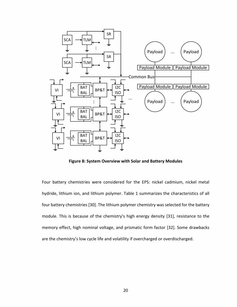
Small satellites and CubeSats have established themselves within the aerospace community because of their low cost and high return on investment. Many CubeSats are developed in a short time frame and often leverage commercial off the shelf components for quick turnaround missions. With regard to the Electrical Power System, commercially available products typically use a centralized architecture. However, a centralized architecture is not reusable, since missions that require additional solar arrays or batteries would necessitate a redesign of the power system. With the range of CubeSat sizes and mission goals, it is obvious that a one-size-fits-all solution is not appropriate. This thesis details a reusable and scalable power system architecture applicable to a variety of missions. Reusability is achieved by using common building blocks or "modules," where the same modules can be used between missions. Scalability is achieved by not limiting the number of modules that can be connected together—more modules can be added as needed. In this system, solar arrays and battery units connect directly to a common bus, supplying an unregulated voltage to each subsystem. These subsystems then regulate the bus voltage to their individual needs. The power system also features direct energy transfer and solar-only operation. KEYWORDS: Small Satellites, CubeSats, Electrical Power System, Direct Energy Transfer,
Distributed Power System
Timothy Lim
July 14, 2016
A MODULAR ELECTRICAL POWER SYSTEM ARCHITECTURE FOR SMALL SPACECRAFT
By
Timothy Meng Lim
Dr. James E. Lumpp
Director of Thesis
Dr. Cai-Cheng Lu Director of Graduate Studies
July 14, 2016
iii
ACKNOWLEDGEMENTS
I would like to acknowledge the support of Kentucky EPSCoR and the Kentucky Space
Grant Consortium for allowing me to perform research in an area of interest and allowing
me to achieve my educational goals.
I would like to thank Dr. James Lumpp for his support and advice during my graduate
studies. Without his invitation to join his research laboratory I would not have been able
to enjoy many opportunities and experiences throughout my college career. I would also
like to thank Dr. Aaron Cramer and Dr. Samir Rawashdeh for their patience, insight, and
support through all of the grant proposals and hardware development.
I would like to thank my colleagues from the Space Systems Laboratory who have directly
influenced my growth as an engineer. From soldering to populating circuit boards, they
have taught me everything I know as an engineer. Our group outings were great
experiences as well. I will never forget our times hanging out at conferences or being able
to witness the launch of our satellite.
Finally, I would like to thank my family for allowing me the opportunity to achieve my
goals. I want to thank my parents for supporting me during my pursuit of a college degree.
I want to thank my sister for always being there when I needed her. I really appreciate
the support you all have given me.
iv
TABLE OF CONTENTS
ACKNOWLEDGEMENTS ....................................................................................................... iii
LIST OF TABLES ................................................................................................................... vii
LIST OF FIGURES ................................................................................................................ viii
1.0 Introduction ............................................................................................................. 1
2.0 Background .............................................................................................................. 6
3.0 Distributed Topology ............................................................................................. 10
4.0 Proposed Power System ........................................................................................ 13
4.1 Solar Module ...................................................................................................... 15
4.2 Battery Module .................................................................................................. 18
4.3 Payload Module ................................................................................................. 24
5.0 Distributed EPS Prototypes .................................................................................... 29
5.1 Solar Module ...................................................................................................... 29
5.1.1 Solar Cells .................................................................................................... 29
5.1.2 Telemetry .................................................................................................... 31
5.1.3 Synchronous Rectifier ................................................................................. 34
5.2 Battery Module .................................................................................................. 35
5.2.1 Battery ......................................................................................................... 35
5.2.2 Battery Protection ....................................................................................... 36
v
5.2.3 I2C Isolation ................................................................................................ 40
5.2.4 Voltage Isolation ......................................................................................... 41
5.2.5 Battery Balancing ........................................................................................ 43
5.3 Payload Module ................................................................................................. 44
5.3.1 Voltage Regulator ....................................................................................... 45
5.3.2 Telemetry .................................................................................................... 48
5.3.3 Load Protection and Control ....................................................................... 50
5.3.4 GPIO Expander ............................................................................................ 57
6.0 Experimental Procedures ....................................................................................... 59
6.1 Solar Module ...................................................................................................... 62
6.2 Battery Module .................................................................................................. 62
6.3 Payload Module ................................................................................................. 62
6.4 Solar Module, Payload Module .......................................................................... 63
6.5 Battery Module + Battery Module, Payload Module ......................................... 63
6.6 Solar Module, Battery Module + Battery Module ............................................. 63
6.7 Solar Module, Battery Module + Battery Module, Payload Module ................. 63
7.0 Discussion............................................................................................................... 64
7.1 Solar Module ...................................................................................................... 64
7.2 Battery Module .................................................................................................. 65
vi
7.3 Payload Module ................................................................................................. 66
7.4 System Testing ................................................................................................... 69
8.0 KySat-3 ................................................................................................................... 73
8.1 Design ................................................................................................................. 74
8.2 Testing ................................................................................................................ 76
9.0 Conclusion .............................................................................................................. 80
References ........................................................................................................................ 82
Vita .................................................................................................................................... 87
vii
LIST OF TABLES
Table 1: Battery Chemistry Comparison ........................................................................... 21
Table 2: Prototype Testing Results ................................................................................... 60
viii
LIST OF FIGURES
Figure 1: KySat-1 ................................................................................................................. 4
Figure 2: KySat-2 ................................................................................................................. 5
Figure 3: Diagram of a Centralized Architecture ................................................................ 8
Figure 4: Diagram of a Distributed Architecture .............................................................. 13
Figure 5: Solar Module Block Diagram .............................................................................. 15
Figure 6: System Overview with Solar Module ................................................................. 16
Figure 7: Battery Module Block Diagram .......................................................................... 19
Figure 8: System Overview with Solar and Battery Modules ........................................... 20
Figure 9: Payload Module Block Diagram ......................................................................... 24
Figure 10: System Overview with Solar, Battery, and Payload Modules ......................... 25
Figure 11: Solar Module Prototype ................................................................................... 29
Figure 12: TrisolX Solar Cell [33] ....................................................................................... 30
Figure 13: ADC Circuit ....................................................................................................... 31
Figure 14: Synchronous Rectifier Circuit ........................................................................... 34
Figure 15: Battery Module Prototype ............................................................................... 35
Figure 16: PL544792-2C Lithium Polymer Battery [37] .................................................... 36
Figure 17: Battery Protection Circuit ................................................................................ 38
Figure 18: I2C Isolator Circuit ............................................................................................ 40
Figure 19: Voltage Isolation Circuit ................................................................................... 42
Figure 20: Battery Balancing Circuit .................................................................................. 43
Figure 21: Payload Module Prototype .............................................................................. 45
ix
Figure 22: Linear Regulator Circuit ................................................................................... 46
Figure 23: Step-up Converter Circuit ................................................................................ 47
Figure 24: Step-down Converter Circuit ........................................................................... 48
Figure 25: Telemetry Circuit ............................................................................................. 49
Figure 26: Load Protection and Control Circuit ................................................................ 51
Figure 27: Alternative Payload Protection and Control Circuit ........................................ 54
Figure 28: GPIO Expander Circuit ...................................................................................... 57
Figure 29: Test Setup for Payload Module ....................................................................... 67
Figure 30: Payload Module 5 V Startup ............................................................................ 68
Figure 31: Payload Module 3.3 V Startup ......................................................................... 69
Figure 32: Common Bus Voltage and Payload Module Outputs for System Testing ....... 70
Figure 33: KySat-3 Electrical Power System ...................................................................... 75
Figure 34: EPS Testing ....................................................................................................... 78
1
1.0 Introduction
Before the CubeSat standard was developed, research groups had some difficulty in
performing microgravity experiments. It was a rigorous and time consuming procedure
for any group to put hardware into a space environment due to the process of designing
systems, assembling the components, then getting equipment verified for launch. In the
year 1999, the CubeSat standard was developed to enable space research by groups
without strong aerospace experience. Dr. Jordi Puig-Suari of California Polytechic State
University and Dr. Robert Twiggs of Stanford University introduced the standard to allow
more groups around the world to perform experiments in a space environment [1], to
develop skills necessary for satellite development [2], and to keep development and
launch costs low [3] [4]. The mechanical standards meant that a universal launcher could
be used to jettison satellites into space even though all of the satellites in the launcher
may be designed by different groups around the world.
Because the cost to develop [5] and launch a CubeSat is much lower than a large satellite
[6], experiments performed by a CubeSat are typically higher-risk [4]. These experiments
tend to be unfeasible or unjustifiable on a larger satellite, but are an acceptable risk for
the low cost CubeSat, such as a solar sail or experimental thrusters. CubeSats have been
developed by academia and commercial groups. Even Kickstarter campaigns have been
created for a CubeSat project [7].
2
The CubeSat was designed to minimize risk to the rest of the launch vehicle and other
payloads. The standardized form factor eliminates the amount of work previously needed
to mate a satellite with its launcher [3]. This enables rapid replacements of satellites in
the launcher and allows for a group to take advantage of a launch opportunity quickly
without worrying about physical compatibility issues [8]. CubeSats are typically the
secondary payload on a launch vehicle [9], riding along for missions such as International
Space Station resupply runs and launching of telecommunications satellites [4].
The basic form factor of the CubeSat is a single cube with dimensions of 10 cm x 10 cm x
10 cm with a maximum mass of 1.33 kilograms [10]. This is considered a 1U (one unit).
Other CubeSat sizes are derived from the base unit, such as 0.5U, 1.5U, 2U, 3U, 6U, and
12U. The form factor is relatively small so that multiple CubeSats can be launched at once
using a single launcher [3].
The typical launcher for a CubeSat is called a Poly-PicoSatellite Orbital Deployer (P-POD).
The P-POD consists of a spring loaded plate and a controllable door [8]. As the launch
vehicle approaches the correct altitude, a command is given to the P-POD to open the
door and jettison the payload. CubeSats can also be launched by hand in the case of
Chasqui-I [11].
Radiation mitigation is usually minimal in CubeSats because in Low Earth Orbit (LEO), the
satellite is only in space for 24 months. In this timeframe, consumer electronics are stable
3
enough for normal operation. For a CubeSat to tolerate radiation for more time radiation
hardened components are needed, which are typically too costly for a CubeSat mission
[4].
The rate at which CubeSats have been launched has been increasing and expected to keep
increasing in the future. From the years 2003 to 2012, 100 total CubeSats were launched
into space. Just in the year 2013, 100 CubeSats were launched, roughly ten times the
yearly average of the ten previous years. Extrapolations put the estimated number of
CubeSat launches to increase to 200 to 700 per year for the next 30 years [12]. The short
development timeframe combined with the architecture’s low cost to design and launch
means that the CubeSat platform will probably remain popular for the near future.
At the University of Kentucky Space Systems Laboratory, two CubeSats have been
developed and launched, KySat-1 and KySat-2. KySat-1 was launched in 2011, but failed
to enter orbit when the payload fairing of the Taurus rocket failed to separate. A picture
of KySat-1 is shown in Figure 1. KySat-1 was a 1U CubeSat that was designed for
educational outreach by allowing mobile ground stations to contact and converse with
the satellite [13]. These mobile ground stations would be taken to various schools around
the state of Kentucky so that students could interact with the satellite.
4
Figure 1: KySat-1
KySat-2 was launched in 2013, but unlike KySat-1, the launch was successful. A picture of
KySat-2 is shown in Figure 2. KySat-2 was a 1U CubeSat that was fairly similar to KySat-1,
with the main physical difference being the deployable solar panels on four of its faces.
KySat-2 continued the goal of educational outreach to students across Kentucky, with
another goal of testing a novel system called a stellar gyroscope that utilized an onboard
camera and a sequence of star pictures to determine the satellite’s attitude [14]. KySat-
2 was heard across the world from countries such as Russia, Japan, Argentina, and
Australia but unfortunately the satellite would not accept any commands sent to it from
the ground. The satellite remained in space for two years before finally deorbiting and
reentering the atmosphere.
6
2.0 Background
The hardware in a CubeSat is very similar to the systems found in larger satellites. Typical
CubeSat subsystems include: the Command and Data Handling (C&DH) system, the
Electrical Power System (EPS), communication hardware, the Attitude Determination and
Control System (ADCS), the propulsion system, and a camera. These subsystems can
either be designed in-house by the CubeSat developers or purchased from a third party
vendor specializing in CubeSat system design [4].
This work focuses on the EPS. The EPS is responsible for generating, storing, and supplying
energy to the rest of the satellite [15]. Due to space constraints, certain components such
as batteries and solar arrays are scaled down to fit, but they still serve the same purpose
as they would in a larger satellite.
There are various companies that offer EPS solutions for developers that are not willing
to develop an EPS on their own [4]. Examples of these companies include Clyde Space,
Pumpkin, and CubeSatKit. Their EPS units are fairly standardized, with components such
as voltage regulators already chosen for the customer. When using these commercial-
off-the-shelf (COTS) systems, the developers must take into account the compatibility
between the EPS and the other subsystems the developer plans to use. The COTS EPS
may not be able to handle a payload that requires a unique voltage rail or a large power
draw without some modification.
7
KySat-1 used a COTS EPS from Clyde Space [16]. The EPS provided connections for six
solar panels, a battery, a 3.3 V voltage rail, and a 5 V voltage rail. The rails could be
monitored and turned on or off as needed. Telemetry from the unit includes electrical
data such as rail voltage, rail current, temperature, and battery charge status. The solar
arrays were made from SpectroLab triple junction GaAs TASC cells.
KySat-2 contained a custom EPS unit developed by Morehead State University. The EPS
used three 18650 Lithium-ion batteries for energy storage and used Direct Energy
Transfer as the solar array interface [17]. Two voltage rails were provided, one at 3.3 V
and the other at 5 V. Telemetry data from KySat-2’s EPS was similar to KySat-1’s EPS. The
solar arrays were also designed and assembled by Morehead State University.
Whether a CubeSat EPS is a custom design or a commercial-off-the-shelf design, the
typical EPS architecture is centralized [18], as shown in Figure 3, where solar panels,
batteries, and satellite payloads all tie into a single circuit board. Specific voltage rails are
supplied to each subsystem that requires a given voltage.
8
...
...
...
...
Bat
tery
Sola
r A
rray
Payload Payload
Payload Payload
Sola
r A
rray
Sola
r A
rray
Bat
tery
Bat
tery
Electrical Power System
Battery Bus
Payload Voltage Rail
Solar Array Bus
Figure 3: Diagram of a Centralized Architecture
This type of EPS architecture is prevalent in small satellites due to the simplicity of its
design [18], its physical space efficiency [18], and the availability of COTS designs [19] [20]
[21]. However, there are disadvantages to the centralized architecture. One drawback is
that a centralized EPS’s regulators are designed for the worst case current draws of all the
payloads attached to the regulator, which means the regulator is not operating at the
optimal point on its efficiency curve during normal operation [18]. Another drawback is
in the centralized architecture’s lack of reusability; major design changes may need to be
9
made before a previous EPS design can be used again for another mission [19]. As the
required subsystems for a mission change, the original EPS is either less efficient for the
new requirements or is rendered completely unusable for the new mission [18]. For
groups developing a simple small satellite, a centralized power system architecture is
acceptable. However, in more complex small satellite designs the centralized architecture
is not always practical due to the architecture’s lack of customization.
This work first describes the distributed power system topology, which is efficient,
reusable, fault tolerant, and can be customized as needed. Then, a reference power
system implementation is presented that is based on the distributed power system
principles. After that, testing on the reference implementation is described with the
experimental results explained to show the effectiveness of the distributed architecture.
Finally, the distributed EPS used in the CubeSat KySat-3 is detailed as a real-world use of
the distributed topology principles.
10
3.0 Distributed Topology
The distributed power system topology is commonly used on more complicated
electronic systems, such as medium/large satellites and aircraft [22] [23]. The typical
characteristic of a distributed power system is a high voltage bus supplied throughout the
system [24], where subsystems that require power connect to the bus and then condition
and regulate energy for themselves [22].
In aircraft, typical distributed bus voltages have progressed from 28 V DC to 115 V AC to
270 V DC [23]. In the case of the International Space Station, a 120 V bus is used [22].
Supplying a higher voltage and a lower current throughout the system minimizes the
energy loss due to the distribution of the energy itself, as a higher current at a lower
voltage would incur more loss through the resistance of the connections.
The benefits of the distributed topology include scalability, reusability, efficiency, and
fault tolerance [23]. Scalability is enabled by the distributed bus. A subsystem needing
energy from the bus simply needs an interface engineered between the subsystem and
the bus. The only limitation on the number of subsystems is the total power available
from the bus rather than the total power available from a regulator in the case of a
centralized EPS. A single distributed topology is suitable for a wide variety of missions.
Reusability is related to scalability. If the subsystem interface is properly engineered, the
subsystem and its interface can be used in any system that matches the distributed bus
11
for which it was designed. The interface only needs to be redesigned if the distributed bus
has changed; otherwise, no modifications are necessary. Subsystems used in previous
missions can be used in any combination as needed for future missions.
The distributed power system is efficient as well. Because the subsystem interface is
designed solely for the subsystem, the power conditioning and regulation circuits can be
designed for maximum efficiency when the subsystem is operating normally. In a
centralized power system, the common regulator will not be operating at its optimal point
if some of the subsystems attached to the regulator are inactive.
Because each subsystem is responsible for its own power conditioning and regulation, a
subsystem anomaly is less likely to have an effect on neighboring subsystems. In a
distributed topology, if a subsystem overloads its voltage regulator by drawing too much
current, it is unlikely that other subsystems on the bus will be affected. Contrasting that
behavior with the same situation on a centralized bus, the same overloaded regulator
would interrupt the power supply to all other subsystems connected to that regulator,
potentially jeopardizing the satellite’s mission.
One disadvantage to the distributed power topology is that the topology needs extra
circuitry to interface subsystems to the distributed bus. The additional circuitry is required
to perform the individual subsystem power conditioning and regulation. More
components typically introduce more points of failure in an electronic system. In a small
12
satellite, the extra circuitry takes up more physical volume, which can result in a shortage
of space for other satellite subsystems. Another disadvantage is due to the nature of
switching regulators. These regulators look like negative impedances to the distributed
bus because they are a constant power load. This may cause instability in the bus [25]
[26]. Finally, a distributed power system requires more customization, since each
subsystem interface is unique. The time required to properly design a distributed power
system may not be available to all small satellite developers.
The distributed power system topology offers many benefits when compared to a
centralized architecture, but designing a fully distributed electrical power system may not
be possible for a typical group interested in developing a small satellite. A solution is
presented in this work that combines the benefits of centralized and decentralized
architectures, enabling the proposed small satellite power system to have scalability,
efficiency, and fault tolerance while also being simple to prepare for all types of missions.
13
4.0 Proposed Power System
In the EPS design described herein, distributed topology concepts are applied to the
design of a small satellite power system. This is realized by supplying an unregulated
voltage bus throughout the power system. The various subsystems of the satellite are
connected to the unregulated bus. Solar cells and secondary batteries are attached to the
bus as well. The distributed architecture used for the proposed EPS is shown in Figure 4.
...
... ...
...
Battery Module
Sola
r M
od
ule
Payload Module
Payload
Payload Module
Payload
Payload Module
Payload
Payload Module
Payload
Sola
r M
od
ule
Sola
r M
od
ule
Battery Module
Battery Module
Battery Module
Sola
r M
od
ule
Common Bus
Battery Module Battery Module
...
...
Figure 4: Diagram of a Distributed Architecture
The proposed EPS is separated into three types of modules: the solar module, the battery
module, and the payload module. The solar module is responsible for energy generation
and transfer to the common bus. The battery module is responsible for energy storage
and supply. The payload module is responsible for energy regulation and usage.
14
Modularizing the subsystems allows for scalability if the modules are correctly designed.
The three module types can be attached to the common bus in any quantity as dictated
by the mission requirements. The battery modules can even be placed in series with one
another to increase the common bus voltage without losing any functionality.
The standard modules allow for reusability because the design of each module remains
nearly the same across missions. The solar module and battery module are always the
same from mission to mission. The payload module is the only unit that would require
modifications, but only if the common bus voltage changes. Standardization also reduces
the chance that the modules are incompatible with each other when connected to the
common bus.
The three modules are engineered for maximum efficiency as well. For instance,
components used for the solar module are selected so that minimal energy is lost when
energy is transferred from the solar cell to the common bus. Also, the voltage regulator
on the payload module is chosen to be optimal for each individual payload. More energy
can be dedicated towards powering subsystems which is critical for a small satellite’s
power budget.
Distributed electrical power systems for small satellites have been the subject of previous
research. Other researchers have considered the distributed topology to be the best
approach because of its efficiency and ability to be used in multiple classes of satellites
15
[18]. One distributed power system implementation has switching regulators as the
interface between the batteries and the common bus so that the bus voltage can be held
constant [27]. While this solution is very flexible, allowing for bus voltages both above
and below the battery voltage, it is too complicated to justify its use over an unregulated
bus. The proposed EPS is easier to implement with similar functionality.
The following three sections describe the three module types in more detail.
4.1 Solar Module
The solar module is responsible for energy generation and transfer in the distributed EPS.
The block diagram in Figure 5 details the major components in the module.
Synchronous Rectifier
Telemetry
Solar Cell Array
EPS 5V
Common Bus
EPS I2C
Solar Cell Array
Figure 5: Solar Module Block Diagram
Figure 6 shows the system overview with the simplified solar module added.
16
SR
TLMSCA
SR
TLMSCA
...
... ...
...
Battery Module
Payload Module
Payload
Payload Module
Payload
Payload Module
Payload
Payload Module
PayloadBattery Module
Battery Module
Battery Module
Common Bus
Battery Module Battery Module
...
...
Figure 6: System Overview with Solar Module
Solar cells attached to the solar module generate energy to be used by the rest of the EPS.
The generated energy from the solar cells then needs to be transferred to the rest of the
EPS through the unregulated bus. This should be done efficiently because energy is sparse
in a satellite environment. In addition, the interface should prevent voltage backfeed
from the unregulated bus onto a solar string in the shade.
There are two methods generally used for the energy transfer from the solar cell array,
maximum power point tracking (MPPT) and direct energy transfer (DET). MPPT uses a
switching converter to manipulate the operating point of the solar array so that the solar
array always sees an ideal load, making the energy transfer very efficient. The isolation
17
between solar arrays provided by the MPPT interface allows multiple solar arrays to be
connected to a single bus. MPPT is used in some COTS EPS units and also in custom EPS
units for various CubeSats as well [28]. In contrast, DET uses a diode as the interface
between the solar array and its load. The load then directly determines the operating
point of the solar array, which may or may not be at the optimal point for maximum
power transfer. The interface diode allows multiple solar arrays to be connected to a
single bus similarly to MPPT. The diode prevents voltage backfeed onto any solar string
in the shade.
In previous work at the University of Kentucky Space Systems Laboratory it was found
that a DET solar array interface with a synchronous rectifier is more efficient, more
reliable in a radiation environment and is not affected by the rotation dynamics of the
spacecraft, which greatly hinder MPPT [29]. The advantages of DET in typical operating
conditions make it the ideal choice for the proposed EPS.
In the reference implementation of the distributed EPS, telemetry can be gathered
through a quad input analog to digital converter (ADC) integrated circuit (IC). One
differential input is dedicated to measuring the voltage of the solar array and another
differential input is dedicated to measuring the voltage across a current sense resistor in
series with the solar array. The remaining two inputs are unused, allowing a sun sensor
or a temperature sensor to be attached to the ADC. This extra data could be useful to the
18
operators of the satellite. For example, the solar panels themselves could also be used as
a sun sensor.
The ADC communicates through Inter-Integrated Circuit (I2C), a communication protocol
popular for embedded systems. I2C is a bi-directional open-drain protocol that is
advantageous for modular system design.
The telemetry circuits do require an external voltage rail to operate, because the
telemetry circuits need a reference voltage to determine the amplitude of the signal they
are sampling. This allows the solar module to have the ability to report telemetry even
when sunlight does not shine on the solar array.
4.2 Battery Module
The battery module is responsible for energy storage and energy supply when the solar
arrays are not in sunlight (an eclipse situation). The block diagram in Figure 7 details the
major components in the battery module.
19
Battery Protection
and Telemetry
BATPOS ISO 5V
Local I2C
BATNEG
EPS I2CI2C
Isolation
EPS 5V
PACKNEG
PACKPOS
PACKNEG
Battery Balancing
Voltage Isolation
EPS 5V ISO 5V
PACKNEG
Figure 7: Battery Module Block Diagram
Figure 8 shows the system overview with the simplified solar module and battery module
added.
20
SR
TLMSCA
SR
TLMSCA
...
...
Payload Module
Payload
Payload Module
Payload
Payload Module
Payload
Payload Module
Payload
Common Bus
...
BP&TI2C ISO
BAT BAL
VI
BP&TI2C ISO
BAT BAL
VI
BP&TI2C ISO
BAT BAL
VI
......
Figure 8: System Overview with Solar and Battery Modules
Four battery chemistries were considered for the EPS: nickel cadmium, nickel metal
hydride, lithium ion, and lithium polymer. Table 1 summarizes the characteristics of all
four battery chemistries [30]. The lithium polymer chemistry was selected for the battery
module. This is because of the chemistry’s high energy density [31], resistance to the
memory effect, high nominal voltage, and prismatic form factor [32]. Some drawbacks
are the chemistry’s low cycle life and volatility if overcharged or overdischarged.
21
Table 1: Battery Chemistry Comparison
Battery Chemistry
Energy Density (Wh/kg)
Cycle Life
Nominal Cell Voltage (V)
Memory Effect?
Form Factor
Nickel-Cadmium
45-80 1500 1.25 Yes Cylindrical
Nickel Metal Hydride
60-120 400 1.25 Yes Cylindrical
Lithium Ion 110-160 400-750
3.6 No Cylindrical
Lithium Polymer
100-130 400 3.6 No Prismatic
Lithium polymer batteries require strict protection because they are very volatile when
stressed outside its limits. The protection circuit used in the battery module handles
overvoltage protection, undervoltage protection, and overcurrent protection (charge and
discharge). When the battery is in an overvoltage condition, the charge current path is
blocked, only allowing a discharge current from the battery. When the battery is in an
undervoltage condition, the discharge current path is blocked, only allowing a charge
current into the battery. When the battery is in a charge overcurrent condition, both the
charge and the discharge current paths are blocked. The protection circuit then delays for
a specific amount of time before checking if the battery’s voltage is greater than the
voltage supplied to the battery. If so, both of the current paths are reestablished. When
the battery is in a discharge overcurrent condition, the discharge current path is blocked.
The protection circuit then delays for an amount of time before checking if the battery’s
voltage is less than the voltage supplied to the battery. If so, the current path is
reestablished.
22
To achieve scalability, the battery modules must be able to be placed in any series or
parallel combination. This presents two challenges that must be overcome: cell balancing
and telemetry gathering.
When batteries are placed in a series string, variances in manufacturing and inherent
battery characteristics mean that the batteries could be charging and discharging at
different rates, even though their specifications are the same. This could result in eventual
battery protection lockouts because one battery in a string could be in an overvoltage
condition and another battery in an undervoltage condition. In this situation, a charge
current to the string is not possible because of the overvoltage battery. Conversely, a
discharge current from the string is not possible because of the undervoltage battery. The
string would be locked out from use by the EPS until the overvoltage battery slowly self-
discharges.
To avoid this situation, a cell balancing circuit was placed on the battery module. The
circuit consists of a zener diode and a resistor placed parallel to the battery. The zener
diode is chosen so that its zener voltage is above normal battery voltages and below the
overvoltage limit. When the battery voltage is above the zener voltage, the zener diode
is in reverse breakdown, allowing current to flow through the diode. This balancing
current is limited by the balancing resistor.
23
As a battery module reaches an overvoltage condition, more current gets shunted
through the balancing circuit. The balancing circuit attempts to regulate all battery
modules to the zener voltage. If one battery charges much faster than the others in its
string, more current is drawn from it as it reaches full capacity. This allows the other
batteries in the string to catch up to its state of charge.
The overall efficiency of the battery modules is then reduced, as some energy is diverted
to balance the batteries. However, additional losses are only realized when the battery is
approaching an overcharge condition and not during normal operation.
Telemetry is useful for operators of the satellite to determine the state of charge of the
battery bank and to decide what actions to take based on that information. The
protection circuit in the reference design provides telemetry through an I2C interface;
however, if battery modules are placed in series, the I2C voltage levels are not referenced
to ground potential. Instead, the levels are referenced to the negative leg of its local
battery. The I2C signals need to be level shifted (both logic high and logic low) so that
communication can be established no matter where the battery module is positioned in
a string. A galvanic isolation IC was connected to each battery module to perform the
required I2C level shifting.
24
4.3 Payload Module
The payload module is responsible for regulating the energy to the other subsystems in
the satellite. The block diagram in Figure 9 details the major components of the payload
module.
GPIO Expander
EPS 5V
EPS I2C
CTL
Voltage Regulation
Common Bus
TelemetryEPS I2C
Load Protection
and Control
VREG To Payload
5V Regulator
EPS 5V
EPS 5V
Common Bus
Figure 9: Payload Module Block Diagram
Figure 10 shows the system overview with the simplified solar module, battery module,
and payload module added.
25
SR
TLMSCA
SR
TLMSCA
Common Bus
...
BP&TI2C ISO
BAT BAL
VI
BP&TI2C ISO
BAT BAL
VI
BP&TI2C ISO
BAT BAL
VI
...
EXP
VR TLM LP&C
5V REG
EXP
VR TLM LP&C
5V REG
Payload
Payload
...
...
...
Figure 10: System Overview with Solar, Battery, and Payload Modules
The main component in the payload module is the voltage regulator. The voltage
regulator converts energy from the unregulated bus to the attached payload and directly
affects the efficiency of the payload module itself. Without the regulator, the payload will
not operate.
There are two methods commonly used for voltage regulation. The first is linear
regulation, where a higher voltage is regulated to a lower voltage. This is done by
dissipating the difference in voltage across the regulator itself. Linear regulators are very
stable and typically have a noise free output voltage. The main disadvantage to linear
regulators is that they are very inefficient due to the excess energy being dissipated by
26
the regulator. Typical efficiency values for linear regulators range between 50% and 70%.
Linear regulators are commonly used for subsystems that do not require much energy
because the low efficiency of the regulator connected to a less demanding load would
have a small impact on the overall power budget.
The second method used for voltage regulation is called a switched mode power supply,
or a switching regulator. Switching regulators can be used to regulate a higher voltage to
a lower voltage (step-down regulator) or regulate a lower voltage to a higher voltage
(step-up regulator). This is done by rapidly switching the voltage across an inductor, with
the components in different configurations depending on the desired result. Not much
energy is wasted to perform the conversion, so switching regulators are very efficient.
Typical efficiency values for switching regulators range from 80% to 95%. However, due
to the presence of a high frequency switch signal, the output voltage from switching
regulators tends to be electrically noisy. The switching regulator circuit is also typically
more complex than linear regulators. Switching regulators are commonly used for
subsystems that demand more power because a low efficiency regulator would waste too
much energy on voltage regulation, which could be detrimental to the overall power
budget.
The payload module also handles payload protection in the form of overvoltage
protection, undervoltage protection, and overcurrent protection. If the regulator
provides a higher or lower voltage than specified by the payload, the protection circuit
27
will cut off the power supply to the payload to avoid accidental damage to the payload. If
the payload starts to draw more current than expected, then the protection will cut off
the power supply to the payload and allow the payload to reset. The protection circuit
also allows for an external source to control the power supply to the payload, so satellite
subsystems can be individually powered on and off. This is useful for energy management
of the satellite or performing hard resets of subsystems.
The payload module also provides telemetry to determine the status of the payload. The
voltage provided to the payload and the current draw of the payload can be obtained
through the telemetry circuits. Like the other two modules, the telemetry circuits in the
payload module use I2C for communication in the reference designs.
In the reference implementation, a general purpose input/output expander is used for
payload control. The expander also uses I2C for communication.
The telemetry circuits and the expander require an external voltage rail to operate. This
means telemetry can be gathered and the payload can be commanded as long as the
payload module can draw energy from the common bus.
The payload modules can be placed in parallel to attach more satellite subsystems to the
EPS. If a subsystem is used again in a future mission, the payload module designed for it
28
can be reused without modification if the unregulated bus is within the payload module’s
specification.
29
5.0 Distributed EPS Prototypes
Prototypes were created for the three types of modules by designing and assembling
printed circuit boards for each module. The overall design was loosely based on the EPS
for the CubeSat KySat-2 so that the prototypes could be tested with the spare hardware.
The following three sections detail the three module prototypes and their circuitry.
5.1 Solar Module
The reference implementation of the solar module prototype consists of the solar cells,
the synchronous rectifier circuit, and the telemetry circuit. Figure 11 shows the solar
module prototype.
Figure 11: Solar Module Prototype
5.1.1 Solar Cells
Solar cells convert solar energy into energy usable by the satellite. The solar cells used in
the reference implementation are supplied from TrisolX. The solar cell chemistry is GaAs
30
with an open circuit voltage of 2.62 V, maximum power voltage of 2.33 V, maximum
power current of 14.6 mA, and an efficiency of 28% [33]. These cells are made from the
cutoffs of larger space rated solar cells, so many of them are needed in parallel to produce
enough current to supply a satellite. Figure 12 shows a single TrisolX solar cell.
Figure 12: TrisolX Solar Cell [33]
The maximum solar string length is set to seven cells, which results in a maximum open
circuit voltage of 18.34 V and a maximum power voltage of 16.31 V. This limit was set
because the reference implementation was designed to be similar to the EPS used on
KySat-2. A larger solar string is possible, but may require some other components further
down the circuit to be changed.
The TrisolX cells cannot produce the same current as the cells used on KySat-2 on their
own, but five sets of TrisolX solar cells in parallel are a good approximation. This results
in a maximum power current of 73 mA. Each solar array produces 1.19 W of power, so a
CubeSat with four solar arrays produces 4.76 W in ideal conditions. More than likely, only
two arrays will be in sunlight at a given time, so the expected production is 2.38 W.
Relative to KySat-2, this is very good because KySat-2 used 2 W of energy. The TrisolX
31
solar arrays would still result in a positive power budget if they replaced the original solar
arrays.
5.1.2 Telemetry
Telemetry is used on the solar module to provide the status of the solar arrays to the EPS.
The telemetry circuit is based on an analog-to-digital converter (ADC). The MCP3428 from
Microchip Technology Inc. was chosen as the solar module’s ADC. The ADC circuit is
shown in Figure 13.
Figure 13: ADC Circuit
The first criteria when selecting an ADC to use was its communication method. The
distributed EPS uses an I2C bus, so the ADC must be compatible with the I2C standard.
The next criteria is the number of I2C addresses the ADC can support and the address
range of the ADC. Because the total number of solar modules connected to the bus is
32
unknown, it is best to choose the ADC that can handle the maximum number of modules
without address interference.
The MCP3428 contains four differential input pairs. The inputs can be sampled with a
resolution up to sixteen bits with a minimum of fifteen samples per second. The MCP3428
can also be placed in one-shot conversion mode where the ADC sleeps after taking a
measurement. This reduces the energy draw of the IC. The MCP3428 has an onboard
voltage reference of 2.048 V. The input voltage range of the IC is 2.7 V to 5.5 V. The
MCP3428 has nine different usable I2C addresses [34].
In the reference implementation, the MCP3428 is powered from an external 5 V rail
because the telemetry should be active as long as the EPS is active. The other option is
to have the ADC powered from the solar array itself, but that would mean when the solar
cells are shaded, the telemetry IC would not receive any power. In this case, the IC would
not respond to an EPS request for telemetry, so the solar string status would be unknown.
In the current implementation, the solar string voltage is always known to the EPS
whether the cells are in sunlight or in shade.
The voltage measurement is connected to Channel 1 of the ADC. It is a single ended
measurement with the negative pin of the differential input connected to GND. The
voltage range of the solar string varies from 0 V to 20 V, which is greater than the voltage
reference and the maximum input voltage of the MCP3428. A voltage divider is used to
33
bring the solar voltage down to a measurable level. The divider made from a 20 kΩ
resistor and a 2 kΩ resistor divides the solar voltage by eleven. The voltage range seen
by Channel 1 is now 0 V to 1.818 V, well within the ADC input voltage limits. The voltage
divider resistors are extremely accurate at 0.01% tolerance so that variance in resistance
minimally affects the accuracy of the measurement. The ADC can sample a measurement
with sixteen bits of accuracy, making the ADC accurate to 0.687 mV after accounting for
the voltage divider. For the voltage measurement, the gain remains at the default setting
of one.
The current measurement is connected to Channel 2 of the ADC. It is a differential
measurement, with the positive pin of the differential input on the solar voltage side and
the negative pin of the differential input on the bus voltage side. Voltage dividers used
for the voltage measurement are used again for the current measurement to bring the
voltage range down to a measurable level. The estimated accuracy of the current
measurement is 3.43 mA at a resolution of sixteen bits and a gain of eight.
The voltage supplied to the Adr pins on the IC determines the I2C address of the
MCP3428. The Adr pins can be connected to Vdd, Vss, or left floating. This results in nine
possible I2C addresses for the MCP3428.
34
5.1.3 Synchronous Rectifier
The synchronous rectifier is used to efficiently transfer energy from the solar cells to the
unregulated bus. The synchronous rectifier used in the reference implementation is
based on the LTC4412HV integrated circuit from Linear Technology. The synchronous
rectifier circuit is shown in Figure 14.
Figure 14: Synchronous Rectifier Circuit
The main criteria when selecting the synchronous rectifier was the input voltage range.
The solar string can range from 0 V to 20 V, so the synchronous rectifier circuit must be
able to accept all voltages within that range.
35
The LTC4412HV has an absolute voltage rating of -14 V to 40 V, which covers the voltage
range of the solar string [35]. The MOSFET used for the energy transfer is the Si4423DY
from Vishay Siliconix. The MOSFET is P-type with a maximum Vds of -20 V and a maximum
drain current of -10 A [36], which covers the expected voltage and current ranges of the
solar cells. The turn on voltage is at most -0.9 V and the expected on-state resistance is
no greater than 0.0115 Ω at a Vgs of -1.8 V.
5.2 Battery Module
The reference implementation of the battery module prototype consists of the battery,
battery protection circuit, I2C isolator, the voltage isolator, and the battery balancing
circuit. Figure 15 shows the battery module prototype.
Figure 15: Battery Module Prototype
5.2.1 Battery
The battery stores excess solar energy from the solar cells and supplies energy to the
satellite when the solar arrays are shaded. The main criteria when selecting the battery
is the battery capacity and the physical dimensions of the cell. One of the design goals is
to have the ability to place two batteries side by side inside the satellite, so a single cell
36
must be smaller than 100 mm x 50 mm in length and width. The battery selected for the
reference implementation is the Lithium polymer PL544792-2C from BatterySpace,
shown in Figure 16.
Figure 16: PL544792-2C Lithium Polymer Battery [37]
The PL544792-2C has a nominal voltage of 3.7 V, capacity of 2500 mAh, and dimensions
of 92.5 mm x 47 mm x 5.4 mm [37]. Its cycle life is greater than 500, with charge rate of
0.5 C and discharge rate of 2.0 C. The mass of the battery is 51 g. The Lithium-polymer’s
prismatic form factor helps reduce the amount of physical space the batteries fill in the
satellite, so more room can be made for other hardware.
5.2.2 Battery Protection
The Lithium polymer battery chemistry chosen for the reference implementation is very
volatile when the cell is overcharged or overdischarged. A dedicated battery protection
circuit is needed for each cell to make sure the batteries remain within the bounds of
normal operation. Therefore, the battery protection circuit must disable the battery
when overcharged, disable the battery when overdischarged, and only monitor one cell
per circuit. The single cell per circuit criteria is driven by the scalability of the distributed
37
EPS; if more voltage is needed on the unregulated bus then battery modules need to be
easily added in series with each other without modification to the circuit. Finally, the
battery protection circuit needs to provide telemetry for data such as the battery voltage
and battery current. An all-in-one IC means there are fewer parts to assemble on the
circuit board and fewer components that could fail in the space environment. The
telemetry would need to be accessed through I2C, so the option of multiple I2C addresses
is necessary as well.
The battery protection circuit chosen for the reference implementation is based on the
DS2764 from Maxim Semiconductor. The battery protection circuit is shown in Figure 17.
39
The DS2764 protects the battery from overvoltage, undervoltage, and overcurrent/short
circuits [38]. The IC provides telemetry in the form of battery voltage, battery current,
and temperature through an I2C interface. The DS2764 only monitors a single battery
cell, so multiple ICs can be placed in series as needed.
The battery is disabled in the event of a fault through the Si4933DY dual MOSFET IC. The
Si4933DY has two P-channel MOSFETs on the IC, with a maximum Vds of -12 V and a
continuous current rating of -5.9 A [39]. Its gate threshold voltage is at most -1 V with
maximum on-state resistance of 0.022 Ω at a Vgs of -1.8 V. The DS2764 turns the MOSFETs
on or off depending on the fault condition detected.
The overvoltage limit is always set to 4.35 V, and the undervoltage limit is always set to
2.6 V. The DS2764 uses an external current sense resistor for the overcurrent/short circuit
protection. When the IC sees a voltage difference of 47.5 mV across the sense resistor,
the overcurrent protection kicks in. At the sense resistor value of 0.038 Ω, the
overcurrent limit is 1.25 A, corresponding to a 0.5C charge rate of the battery chosen for
the reference implementation. Overcurrent can be triggered during both charging and
discharging, making the 0.5C charge rate the limiting factor.
The I2C address of the DS2764 is user controlled through the I2C bus. There are no
address limitations, so the DS2764 has 127 possible addresses.
40
5.2.3 I2C Isolation
The I2C telemetry from the battery protection circuit has its voltage levels based on the
battery voltage of the battery the DS2764 protects. When battery modules are placed in
series with one another to increase the unregulated bus voltage, the telemetry from each
DS2764 is on its own set of logic levels. This necessitates the use of an I2C isolator to shift
the various logic levels back down to a single level so that the EPS can correctly receive
telemetry from each battery protection circuit.
The I2C isolator circuit chosen for the reference implementation is based on the Si8600
from Silicon Laboratories. The I2C isolator circuit is shown in Figure 18.
Figure 18: I2C Isolator Circuit
The Si8600 has independent, bidirectional SDA and SCL isolation channels [40]. The
isolation is tolerant of up to 5000 Vrms. Its operating supply voltage is 3 V to 5.5 V. The
Si8600 uses galvanic isolators to isolate the I2C communication signals from each other.
Side A connects to the DS2764 I2C lines, while side B connects to the EPS I2C lines. Side
B is powered by an external voltage supply provided by the EPS. Side A is powered from
41
a voltage isolator using that same external supply. The voltage isolator is detailed in the
next section.
5.2.4 Voltage Isolation
A voltage isolator is not necessary to operate the I2C isolator, but makes telemetry
gathering more available during EPS operation. The alternative power source for the I2C
isolator is directly from the battery connected to the module’s DS2764. However,
because the Si8600’s minimum operating supply voltage is 3 V and the battery
undervoltage limit is 2.6 V, the battery voltage could dip below 3 V but still be above 2.6
V. In this case, the EPS would still continue to operate, but the battery telemetry would
be inaccessible due to the I2C isolator browning out. An external voltage supply is already
being provided to the Si8600 on the EPS side, so a voltage isolator is a simple method to
allow that voltage supply to be used on the DS2764 side of the I2C isolator.
The voltage isolator chosen for the reference implementation is based on the SN6501
from Texas Instruments. The voltage isolation circuit is shown in Figure 19.
42
Figure 19: Voltage Isolation Circuit
The SN6501 uses an external transformer and a rectifying circuit to isolate a given voltage
[41]. The overall circuit converts a DC voltage to AC voltage, applies the AC voltage to a
transformer, and then rectifies the transformed AC voltage back to DC voltage at a new
reference potential. Even if a battery is discharged below 3 V, the I2C isolators will still
operate, providing telemetry throughout the full battery voltage range.
The MBR0520L Schottky diode was used as the rectifying diode. The MBR0520L has a
forward voltage of less than 0.385 V [42]. This is beneficial because less energy is lost
during the rectifying process as compared to a typical diode’s forward voltage of 0.7 V.
The EPS should draw only enough energy as needed to operate so that more energy can
be given to the rest of the systems on the satellite. The transformer’s coil ratio is tuned
so that the rectified output can be immediately used to power the I2C isolator.
43
5.2.5 Battery Balancing
Due to variances in the battery production process, each battery charges and discharges
at a different rate. Over time, this may result in a battery deadlock, where one battery in
a pack is in overvoltage and another battery is in undervoltage. In this case, the pack
cannot charge due to the battery in overvoltage disabling the charge path and the pack
cannot discharge due to the battery in undervoltage disabling the discharge path. The
battery pack is rendered useless until self-discharge brings the battery in overvoltage
down to a normal voltage. A battery balancing circuit was added to the battery module
to minimize the chance of a battery deadlock.
The battery balancing circuit chosen for the reference implementation consists of a Zener
diode and a resistor. The battery balancing circuit is shown in Figure 20.
Figure 20: Battery Balancing Circuit
44
The Zener diode is chosen so that the diode is in breakdown mode before the overvoltage
limit is reached, at 4.35 V. In the reference implementation, the Zener diode chosen is
the KDZTR3.9B, with a minimum Zener voltage of 3.9 V and a maximum Zener voltage of
4.4 V. If the Zener voltage is too low, then the balancing circuit activates early and reduces
the overall battery module efficiency, but if the Zener voltage is too high, the balancing
circuit activates too late and could result in the batteries deviating from the balanced
state much faster. The KDZTR3.9B typically has a Zener voltage of about 4.15 V, which is
perfect for the reference implementation.
The series resistor is used as a current limit, so the maximum balancing current is 17.5
mA. This is much larger compared to a lithium polymer self-discharge rate of 5% a month,
or about 0.173 mA with a battery capacity of 2500 mAh. The battery balancing circuit
may not prevent battery deadlock situations, but if they do occur, the balancing circuit
should bring the pack out of deadlock much faster than it would be if the EPS had to wait
for the batteries to self-discharge.
5.3 Payload Module
The reference implementation of the payload module prototype consists of the voltage
regulator, telemetry circuit, load protection and control circuit, and the GPIO expander.
Figure 21 shows the payload module prototype.
45
Figure 21: Payload Module Prototype
5.3.1 Voltage Regulator
The voltage regulator is used to supply usable energy to the payload connected to the
module. For the reference implementation, three voltage regulators were chosen: one
linear regulator, one step-up converter, and one step-down converter. The regulators
must be adjustable and able to handle an output current of 0.5 A for the linear regulator
and 1 A for the switching regulators. The output current requirements were based on the
EPS used in KySat-2.
The linear regulator chosen for the reference implementation is the LT1763 from Linear
Technology. The LT1763 circuit is shown in Figure 22.
46
Figure 22: Linear Regulator Circuit
The LT1763 can supply 500 mA of current and has a dropout voltage of 300 mV. Its input
voltage range is 1.8 V to 20 V [43]. It is an adjustable regulator so the feedback resistors
can be changed to manipulate the output voltage. The output voltage will adjust until the
voltage seen on the ADJ pin is 1.22 V.
The step-up converter chosen for the reference implementation is the SC4503 from
Semtech Corporation. The step-up converter circuit is shown in Figure 23.
47
Figure 23: Step-up Converter Circuit
The SC4503 can supply 1.4 A and has a constant switching frequency of 1.3 MHz [44]. Its
input voltage range is 2.5 V to 20 V. The maximum output voltage is 27 V. The output
voltage will be adjusted until 1.25 V is seen on the FB pin.
The RSX101VA-30 is a Schottky diode used as a rectifying diode. Its forward voltage is
0.43 V and can handle a reverse voltage of up to 30 V [45]. The diode has a maximum
average rectified forward current of 1 A.
The step-down converter chosen for the reference implementation is the ST1S10 from
STMicroelectronics. The step-down converter circuit is shown in Figure 24.
48
Figure 24: Step-down Converter Circuit
The ST1S10 can supply 3 A and has a synchronizable switching frequency from 400 kHz up
to 1.2 MHz [46]. Its input voltage range is 2.5 V to 18 V. The output voltage range is 0.8
V to its input voltage multiplied by 0.85. The output voltage will be adjusted until 0.8 V is
seen on the Vfb pin.
5.3.2 Telemetry
The payload telemetry circuit gives status information about the payload to the EPS. The
features required for the telemetry circuit are the ability to gather voltage and current
telemetry, an I2C interface, and a selectable I2C address. The telemetry circuit chosen
for use on the reference implementation is the PAC1710 from SMSC. The telemetry
circuit is shown in Figure 25.
49
Figure 25: Telemetry Circuit
The PAC1710 is an integrated circuit designed to measure voltage and current. The IC can
measure voltage and current up to a resolution of eleven bits [47]. The input power
supply range is 3 V to 5.5 V. The PAC1710 can measure a voltage ranging from 0 V to 40
V. The differential voltage between the SENSE pins can range from -80 mV to 80 mV,
allowing the IC to also report the direction of current flow.
50
The I2C address is user-selectable through the ADDR_SEL pin. The address is determined
by the resistor value connected to the pin. The PAC1710 can be set to one of sixteen
possible addresses.
The PAC1710 is powered from an external power supply. With a fairly standard input
power supply range it is very likely the PAC1710 can piggyback off of a voltage regulator
used for a payload. KySat-2 contained a 3.3 V rail and a 5 V rail, both of which would be
compatible with the PAC1710.
5.3.3 Load Protection and Control
Load protection is necessary to turn off the payload when a fault condition occurs. Fault
conditions include overvoltage, undervoltage, and overcurrent. The load protection
circuit for the reference implementation is based on the LTC4361 from Linear Technology.
The load protection circuit is shown in Figure 26.
51
Figure 26: Load Protection and Control Circuit
The LTC4361 provides protection for payloads with a voltage range of 2.5 V to 5.5 V [48].
If the IC detects a transient in the input power supply the LTC4361 will remove the
payload from the power supply until the transient passes. The LTC4361 protects the
payload from a transient up to 80 V. The undervoltage lockout is set to 2.1 V and the
overvoltage lockout is set to 5.8 V.
The limited power supply range is acceptable in the reference implementation because it
was designed to protect payloads similar to the ones in KySat-2. The payloads in KySat-2
52
used either a 3.3 V power supply or a 5 V power supply, both within the protection range
of the LTC4361.
A capacitor was added to the GATE pin so that the inrush current to the payload is limited
when the payload is turned on.
The current sense resistor is used so that the LTC4361 can detect an overcurrent
condition. A 0.025 Ω resistor is used so that the effect of the current sense resistor on
the payload’s power supply is minimized. Once the LTC4361 detects a voltage difference
of 50 mV between the IN and SENSE pins, the MOSFET is turned off and the power supply
disconnected from the payload. At the given sense resistor value, the current limit is 2 A.
After a fault condition, the LTC4361 will automatically restart the payload after a 130 ms
delay. There is another version of the LTC4361 that will keep the payload off after a fault
condition if that is the desired behavior for the mission.
The LTC4361 also features an enable pin so the payload can be externally controlled. This
is useful during EPS bootup because payloads can be individually turned on rather than
all at once, allowing critical subsystems to be powered first.
The MOSFET used in the payload protection circuit is the Si1470DH. The Si1470DH is an
N-channel MOSFET that connects or disconnects the payload to its power supply. It has
53
a maximum drain-source voltage of 30 V and a current rating of 4 A [49]. Its threshold
voltage is no greater than 1.6 V, with a maximum on-state resistance of 0.095 Ω at a Vgs
of 2.5 V.
For a payload outside of the LTC4361’s protection range, an alternative circuit must be
used. The alternative payload protection and control circuit is based on the LTC4365 from
Linear Technology and the FPF2700 from Fairchild Semiconductor. The alternative
payload protection circuit is shown in Figure 27.
55
The alternative circuit functions similarly to the LTC4361 circuit but has an adjustable
protection voltage range.
The first half of the protection circuit is the LTC4365. The LTC4365 handles overvoltage
and undervoltage protection for the payload. The IC controls a pair of N-channel
MOSFETs to connect the payload to its power supply. The LTC4365 has an operating
voltage supply range of 2.5 V to 34 V, with overvoltage protection up to 60 V [50]. An
external resistor divider is used to set the overvoltage and undervoltage limits.
When the UV pin sees a voltage below 0.5 V, the IC will disconnect the payload from its
power supply. Once the voltage on UV rises above 0.525 V and 36 ms have passed, the
payload will be reconnected with the power supply.
When the OV pin sees a voltage above 0.5 V, the IC will disconnect the payload from its
power supply. Once the voltage on OV falls below 0.475 V and 36 ms have passed, the
payload will be reconnected with the power supply.
The LTC4365 contains a SHDN pin that can be used to remove the payload from the power
supply by an external controller.
56
The Si4946 is the dual N-channel MOSFET IC used with the LTC4365. It has a maximum
Vds of 60 V with a continuous current rating of 5.5 A [51]. Its threshold voltage is typically
2.4 V and has a maximum on-state resistance of 0.052 Ω at a Vgs of 4.5 V.
The other half of the protection circuit is the FPF2700. The FPF2700 handles overcurrent
protection for the payload. The IC contains an internal N-channel MOSFET to connect the
payload to its power supply. The FPF2700 has an input voltage range of 2.8 V to 36 V [52],
which is very similar to the voltage range of the LTC4365. An external resistor is used to
set the current limit. The minimum current limit can range from 0.4 A to 2 A. The 20%
current limit tolerance sets the maximum current limit to 3 A.
In an overcurrent condition, the FPF2700 clamps the load current so that it cannot rise
above the current limit set by the external resistor. If the condition lasts for longer than
the FPF2700’s blanking period, the payload is disconnected from its power supply. The
FPF2700 will wait 127.5 ms before reconnecting the payload to the power source. The
FPF2700 also has a thermal shutdown feature if the circuit overheats.
The FPF2700 contains an ON pin that can be used to control the payload from an external
device. The FPF2700 combined with the LTC4365 has virtually the same functionality as
the LTC4361, but with a larger input voltage range and more components. The majority
of CubeSat payloads can be protected with at least one of the two circuits.
57
5.3.4 GPIO Expander
The GPIO expander is used to control the payload protection circuit. Instead of directly
connecting a GPIO pin from the EPS microcontroller to the protection circuit, the
microcontroller can just send a command to the GPIO expander to control the payload.
The GPIO expander chosen for use in the reference implementation is the PCA9672 from
NXP Semiconductors. The GPIO expander circuit is shown in Figure 28.
Figure 28: GPIO Expander Circuit
The GPIO expander must be able to communicate through I2C and have user-selectable
addresses. It also needs to have at least four GPIO pins. This requirement was made
because the reference implementation is based on KySat-2’s EPS, which had four
controllable payloads on the satellite.
58
The PCA9672 contains eight GPIO pins that can sink up to 25 mA of current [53]. The IC
can be assigned one of sixteen different I2C addresses. Its operating supply voltage range
is 2.3 V to 5.5 V.
Like the payload telemetry circuit, the GPIO expander is powered by an external power
supply. The PCA9672 has a fairly standard input power supply range, so it can probably
piggyback off of a payload’s voltage regulator. KySat-2 contained a 3.3 V rail and a 5 V
rail, both of which would be compatible with the PCA9672.
59
6.0 Experimental Procedures
The experimental testing results are summarized in Table 2. SM designates a test that
used a solar module, BM designates a test that used a battery module, and PM designates
a test that used a payload module. A plus sign indicates a module used in series with
another module, and a comma indicates a test that used multiple module types
connected in parallel.
60
Table 2: Prototype Testing Results
Module Type
Test Measurement Expectation Actual Notes
SM Normal
Operation Load Voltage 3.2 V
3.171 V
3.2 V 0.06 A input, 51 Ω load
SM Normal
Operation Load Voltage 10 V 9.95 V
10 V 0.19 A input, 51 Ω load
SM Reverse Solar
Cell Protection
Load Voltage 0 V 0.013
mV 3 V input, 51 Ω
load
SM Reverse Solar
Cell Protection
Load Voltage 0 V 0.013
mV 10 V input, 51 Ω
load
SM Reverse Solar
Cell Protection
Load Voltage 0 V 0.013
mV 20 V input, 51 Ω
load
SM Voltage
Telemetry Input Voltage 4 V
3.943 V
4 V 0.08 A input, 51 Ω load
SM Current
Telemetry Input Current 0.08 A
0.085 A
4 V 0.08 A input, 51 Ω load
BM Voltage
Telemetry Battery Voltage
3.95 V 3.923
V
BM Current
Telemetry Battery Charge
Current 0.6 A 0.66 A
4.3 V input, 0.6 A input
BM Undervoltage
Protection Voltage Limit 2.6 V 2.58 V
3.9 V initial voltage, 0.05 A
discharge current
BM Overvoltage Protection
Voltage Limit 4.35 V 4.37 V
3.5 V initial voltage, 5V
input, 1 A charge current
BM Discharge
Overcurrent Protection
Current Limit 1.45 A 1.23 A 1 A initial discharge current
BM Charge
Overcurrent Protection
Current Limit 1.45 A 1.34 A 1 A initial charge
current
BM Charge
Balancing Battery Voltage
4.1 V 3.8 V 4.15 V initial voltage, 30
minute runtime
61
Table 2: Prototype Testing Results (continued)
PM Normal
Operation Load Voltage 5 V 4.95 V
7 V 0.1 A input, 51 Ω load
PM Load Control Load Voltage 5 V 4.95 V 7 V 0.1 A input,
51 Ω load
PM Voltage
Telemetry Load Voltage 5 V
4.953 V
7 V 0.1 A input, 51 Ω load
PM Current
Telemetry Load Current 0.1 A
0.0984 A
7 V 0.1 A input, 51 Ω load
PM Normal
Operation Load Voltage 3.3 V 3.13 V
12 V 0.13 A input, 8.1 Ω
electronic load
PM Load Control Load Voltage 3.3 V 3.13 V 12 V 0.13 A input, 8.1 Ω
electronic load
PM Voltage
Telemetry Load Voltage 3.3 V
3.315 V
12 V 0.13 A input, 27.7 Ω
electronic load
PM Current
Telemetry Load Current 0.119 A
0.118 A
12 V 0.13 A input, 27.7 Ω
electronic load
SM, PM Normal
Operation Load Current 0.4 A
0.399 A
9 V 1 A input, 0.4 A electronic load
BM + BM, PM
Normal Operation
Load Current 0.4 A 0.398
A 0.4 A electronic
load
BM + BM, PM
Undervoltage Protection
Verification Y Y
0.4 A electronic load, test ran until 0 A load
current
SM, BM + BM
Normal Operation
Battery Charge Current
1.0 A 1.0 A 9V 1 A input
SM, BM + BM
Charge Balancing
Battery Voltage
8.2 V 8.24 V 8.3 V initial voltage, 5
minute runtime
SM, BM + BM
Overvoltage Protection
Verification Y Y 9 V 1 A input,
test ran until 0 A input current
SM, BM + BM,
PM
Normal Operation
Battery Charge Current
0.6 A 0.6 A 9 V 1 A input, 0.4 A electronic load
62
Table 2: Prototype Testing Results (continued)
SM, BM + BM,
PM
Normal Operation
Battery Discharge Current
0.2 A 0.2 A 9 V 0.2 A input, 0.4 A electronic
load
SM, BM + BM,
PM Telemetry Verification Y Y
Communication was possible
with all modules in the system
6.1 Solar Module
Various tests were performed on the solar modules including normal operation, reverse
solar cell protection, and a telemetry test. Two solar modules were placed in parallel and
tested for correct operation.
6.2 Battery Module
The tests for the battery module focused on the battery protection circuit which includes
overvoltage protection, undervoltage protection, overcharge current protection, and
overdischarge current protection. Other tests performed include verifying the charge
balancing circuit and telemetry. Two sets of battery modules were then placed in series
with one another with the two sets in parallel to test for correct operation.
6.3 Payload Module
The tests for the payload module include normal operation, load control, and a telemetry
test. These tests were performed for a payload module with a 5 V voltage regulator and
a payload module with a 3.3 V voltage regulator. Two payload modules were connected
in parallel to test for correct operation.
63
6.4 Solar Module, Payload Module
The main test for the solar module and payload module in parallel was for normal
operation.
6.5 Battery Module + Battery Module, Payload Module
The two tests performed on the two battery modules in series with a payload module in
parallel were for normal operation and undervoltage protection.
6.6 Solar Module, Battery Module + Battery Module
The tests performed on the solar module in parallel with two battery modules in series
were normal operation, charge balancing, and overvoltage protection.
6.7 Solar Module, Battery Module + Battery Module, Payload Module
The tests performed on a solar module in parallel with two battery modules in series and
a payload module were normal operation while the batteries were charging, normal
operation while the batteries were discharging, and a telemetry test.
64
7.0 Discussion
The following four sections describe the results from the individual prototype testing and
the testing of prototype combinations.
7.1 Solar Module
The experimental results for the solar module prototype indicate that the solar module
correctly transfers energy from the solar cells while minimizing power loss due to the
transfer. The voltage drop from the synchronous rectifier was measured to be 0.05 V for
the higher input current. The synchronous rectifier efficiency is critical in small satellite
applications, where energy consumption must be minimized.
The tests for reverse solar cell protection and telemetry were successful as well, meaning
that the solar module performed as expected.
The solar modules tested in parallel worked as expected with the synchronous rectifier
circuit preventing voltage backfeed from damaging the solar array. Telemetry was
received from each module as well.
The efficiency of the solar module prototype is 99.5%, which is slightly less than the
expected efficiency, 99.82%. A potential cause of the efficiency discrepancy is the
telemetry circuit, where the sampling frequency is higher than necessary.
65
7.2 Battery Module
The experimental results for the battery module indicate that the battery module
correctly protects its battery from overvoltage, undervoltage, charging overcurrent, and
discharging overcurrent. Also, charge balancing and the telemetry circuits were verified
to be operational.
The measured current limits for current protection seemed to deviate somewhat from
the programmed current limit values. This may be due to the inaccuracy of the current
sense resistors. The variances in resistance could be affecting the overcurrent protection
limit. Another possibility is the resistance of the traces on the PCB affecting the voltage
measured by the protection IC.
The efficiency of the battery module prototype is 83.08%, which is less than the expected
efficiency, 88.73%. The difference could be attributed to the non-ideal characteristics of
the battery protection circuit because of the losses through the components that connect
the battery to the common bus.
The sets of batteries in series then placed in parallel were confirmed to protect each
individual cell from overvoltage, undervoltage, overcharge current, and overdischarge
current. The charge balancing circuits were operational no matter the cell’s position in
the pack and telemetry was responsive even when cells were located above other cells in
series.
66
7.3 Payload Module
The experimental results for the payload module indicate that the payload module
correctly regulates energy for its load, that it has the ability to control the energy path to
the load, and that its telemetry circuits are operational.
The efficiency of the payload module prototype with a linear regulator is 63.94%, which
is slightly less than the expected efficiency, 66.76%.
The efficiency of the payload module prototype with a switching regulator is 82.3%, which
is slightly less than the expected efficiency, 84.69%.
As expected, there is a correlation between voltage regulator efficiency and payload
module efficiency, because the supporting circuits in the payload module draw much less
power than the regulator does. Therefore, the efficiency equation for the payload module
is dominated by the voltage regulators.
The two payload modules in parallel operated correctly. Voltage was regulated to the
proper levels for each payload module without any instability seen. Telemetry was
received from each module.
An extra test was performed on the payload module to analyze the payload module’s
startup. The test setup is shown in Figure 29.
67
SR
TLMPower Supply
EXP
VR TLM LP&C
Payload
Figure 29: Test Setup for Payload Module
The first test used a linear regulator set at 5 V. The test results are shown in Figure 30.
This figure shows the voltage on the common bus and the output of the voltage regulator
when the module is starting up. As the payload module is connected to the solar module,
there is a small downward spike on the bus voltage. A large voltage transient is seen on
the output of the voltage regulator, where the regulator voltage rises to 6.5 V before
settling down to 5 V. Approximately 150 ms after the payload module is turned on, the
payload’s voltage begins to increase. This is due to the payload protection circuit, the
LTC4361. The LTC4361 has a typical startup delay of 130 ms before the circuit allows the
payload to turn on. The regulator voltage does not start at 0 V, this is attributed to the
capacitor on the output side of the regulator not having enough time to fully discharge
before the test results were captured.
68
Figure 30: Payload Module 5 V Startup
The circuit has a relatively slow turn on time due to the capacitance on the gate of the
control MOSFET. This capacitance was added to decrease the dV/dt on the payload. At
the end of the waveform, the payload’s voltage settles at the same voltage that the
regulator supplies. At this point the payload is fully activated and is operating normally.
The second test used a switching regulator set to 3.3 V. The test results are shown in
Figure 31. This figure shows the voltage on the common bus and the output of the voltage
regulator when the module is starting up. The results from the 3.3 V payload module test
are comparable to the 5 V payload module. The main differences between the two test
Payload Voltage
Regulator Voltage
Bus Voltage
69
results are the voltage spike seen on the regulator voltage when the 5 V payload module
started up and the expected switching noise seen on the bus voltage, regulator voltage,
and payload voltage on the 3.3 V payload module.
Figure 31: Payload Module 3.3 V Startup
7.4 System Testing
The final test involved one solar module, two battery modules in series, and two payload
modules connected together on a common bus. The input current, common bus voltage,
output voltage of the 5 V payload module, and the output voltage of the 3.3 V payload
module was logged and graphed in Figure 32.
Payload Voltage
Regulator Voltage
Bus Voltage
70
Figure 32: Common Bus Voltage and Payload Module Outputs for System Testing
0 0.5 1 1.5 2 2.5 3
x 104
-0.2
0
0.2
0.4
0.6
0.8
Time (s)
Cu
rre
nt
(A)
0 0.5 1 1.5 2 2.5 3
x 104
-5
0
5
10
Time (s)
Vo
lta
ge
(V
)
Common Bus Voltage
PM 5 V Output
PM 3.3 V Output
71
For 5000 sec, the system was supplied current from the power supply connected to the
solar module. At 5000 sec, the power supply was turned off. The voltage immediately
dropped, due to the difference in charge and discharge curves of the batteries. The
batteries discharge until 22000 sec. The power supply was turned on at this time and the
battery modules immediately started charging.
During the 17000 sec of discharging, the battery modules experienced an undervoltage
condition. This was triggered when the common bus voltage reached 5.4 V, which
corresponds to approximately 2.7 V per battery. The expected undervoltage limit is 2.6 V
[38]. However, the maximum undervoltage detection limit is 2.7 V, which agrees with the
testing results.
The only time that the payload modules were not supplying energy to their payloads was
during the undervoltage condition. At all other times, the payload modules kept their
payloads operating correctly. The experimental results for the three module types on a
common bus indicate that the three module types are compatible when connected in
parallel. Each module performed as expected in the system configurations tested. There
do not seem to be any conflicts between modules even when modules are disconnecting
and reconnecting to the common bus. The telemetry isolation circuits on the battery
module were confirmed to be operating correctly because communication was possible
with the battery module on top of the pack.
72
Even though the 3.3 V payload module looks like a negative impedance to the bus due to
its switching regulator, no bus instability was observed.
73
8.0 KySat-3
KySat-3 is a CubeSat mission currently in progress at the Space Systems Laboratory of the
University of Kentucky. KySat-3 is a 1U CubeSat with deployable solar panels that will be
launched from the International Space Station by use of a Nanoracks launcher in 2016 or
2017. The KySat-3 orbit time is estimated to be a few months, much less than the two
years of KySat-2. The mission goal for KySat-3 is to perform the experiments that were
unsuccessful in the KySat-2 mission, namely the verification of the Stellar Gyroscope
developed by Samir Rawashdeh, a PhD candidate who previously worked in the Space
Systems Laboratory. During the KySat-2 project, two flight models of the satellite were
constructed and tested. One model was chosen for flight and was launched successfully
in 2013. The unused model remained on Earth as a demonstration unit.
In 2015, the Space Systems Laboratory received a grant from NASA to determine the
functionality of the backup model and to prepare the satellite for a mission. The backup
KySat-2 model, now dubbed KySat-3, underwent initial inspection by the Space Systems
Laboratory.
Examination revealed that the solar arrays and the batteries on the back up model were
still usable. However, it was found that the EPS unit in the model was inactive and
unresponsive. Two options were considered for the EPS replacement. The first was to
acquire a working EPS from Morehead State University, the original developers of the EPS
74
for KySat-2. Unfortunately, Morehead State University had a very full schedule working
on their own CubeSat mission, so this option was not possible.
The second option for the EPS was to develop the EPS at the University of Kentucky. At
the time, the distributed EPS prototypes had been fabricated and assembled. Initial tests
had been performed on the prototypes of the distributed EPS; because the results were
promising, the mission planners decided to have a distributed EPS unit fabricated and
assembled for use in KySat-3.
8.1 Design
Most of KySat-3’s EPS design was based off the prototypes of the distributed EPS
reference implementation. The EPS was designed to be a direct drop-in replacement for
Morehead State University’s EPS used in KySat-2, including form factor and connector
layout. The voltage regulators used for KySat-2 [17] were reproduced in KySat-3’s EPS to
reduce the chance of incompatibility with the existing subsystems. The most major
change between the prototypes and the KySat-3 EPS is that each of the modules used in
a fully distributed EPS had to be located on the same PCB since KySat-2 used a single board
EPS. This forced many components together on a single board, meaning that part
placement on the PCB was more difficult. Figure 33 shows the distributed EPS design for
KySat-3.
75
Figure 33: KySat-3 Electrical Power System
The main feature added to KySat-3’s EPS that was not present in KySat-2’s EPS is an inhibit
switch system that utilized the PCB itself. This was achieved by having multiple power
and ground planes on the PCB. These planes were isolated from each other, but routed
to a single connector on the board. All of the inhibit switches in the satellite are wired to
a single connector, and then this connector plugs into the EPS to provide the connection
between the planes. This simplifies the satellite construction because the EPS can be
easily removed from the satellite stack and replaced when needed. There is also only one
connection point for all of the inhibit switches; reducing confusion as to how each inhibit
switch connects to the satellite. In KySat-2, the inhibit switches were soldered directly to
the power line they were inhibiting, which can be hard to keep track of when assembling
the satellite. The method used in KySat-3’s EPS should make connecting the inhibit
switches much easier during satellite assembly.
A microcontroller was added to KySat-3’s EPS so that telemetry could be automatically
gathered from the EPS modules. The Command and Data Handling system would then
76
ask the EPS microcontroller for that data when needed. A programming header was
added to the circuit so the firmware could be updated even when the satellite is
assembled.
A watchdog timer was also added to the EPS. If the EPS microcontroller became
unresponsive for a specified amount of time, the watchdog timer would toggle the reset
pin on the microcontroller and reboot the EPS controller, clearing the fault condition.
8.2 Testing
The same tests performed on the EPS prototypes were repeated on the KySat-3 EPS,
checking for qualities such as functionality, battery protection, load control, and stability.
These tests were successful. Because of the new inhibit switch system, the switches
needed to be connected and actuated before the EPS would work. To make testing easier,
a dummy connector was created that shorted the connection points where the inhibit
switches should be, making the EPS think that the inhibit switches were connected and
actuated. The dummy connector was very effective and simplified the testing process.
One new test performed on the KySat-3 EPS is the verification of the inhibit switch system.
The inhibit switches isolate different parts of the satellite and are used to make sure
certain parts of the satellite do not turn on when they are not supposed to, such as when
the satellite is in the satellite stack. The inhibit switches were tested and the subsystem
isolation performed as expected.
77
Another test involved drawing current from the solar and battery modules. Because all
three module types were located on a single PCB, the total current draw of the satellite
subsystems would have to run through traces on the circuit board. Testing was
performed to make sure these power traces were large enough to handle the current that
could be drawn from the EPS. The results indicate that the EPS correctly operates under
high current draw.
Nanoracks also provided a list of tests to be performed before the satellite could be
integrated. This included visual inspection of the batteries, measurement of battery
characteristics such as open circuit and closed circuit voltages, charge cycling data,
overcharge limits, overdischarge limits, short circuit protection, vibration testing, and
vacuum testing. The KySat-3 EPS also passed these tests.
Figure 34 shows the typical test setup for the KySat-3 EPS. The dummy connector is
connected to the EPS near the bottom of the circuit board. Prototype battery modules
were used to securely connect batteries to the EPS for testing.
78
Figure 34: EPS Testing
Telemetry gathering was more difficult when assembling KySat-3’s EPS than it would have
been for a true distributed EPS. This is because components such as the DS2764 in the
battery module would normally be programmed separately, since each battery module is
removable. KySat-3’s EPS was on a single PCB, so programming the DS2764 would get
complicated because the DS2764 has the same default I2C address and are all on the same
communication bus when the EPS is populated. For this IC, the population of the DS2764
had to be staggered so that one would be populated then programmed. This process
would then repeat for the other two DS2764 ICs.
An Arduino sketch was written to collect the telemetry from the KySat-3 EPS and also to
control the payload modules. First, the program would iterate through all the I2C
addresses of the telemetry ICs and verify that the chips were available for communication.
Then, the user is presented with a menu. The top option is to show the EPS telemetry.
The solar module telemetry is presented, including voltage and current of the solar cells.
79
The battery module telemetry is then displayed, including the voltage and current of its
local battery and temperature of the IC. The telemetry finishes with the payload module
telemetry, including the voltage and current of each payload and the calculated power
draw of each payload.
The next menu option allows the user to turn on a payload module. The EPS starts up
with all payload modules deactivated. The user enters a number that corresponds to the
payload module to be turned on. The program will then display which of the payload
modules are on and which are off.
The final menu option allows the user to turn off a payload module. The user enters a
number that corresponds to the payload module to be turned off. The program will then
display which of the payload modules are on and which are off.
80
9.0 Conclusion
A modular, scalable, easy to reuse EPS for small satellites has been detailed in this work.
The described EPS achieves modularity by dividing the EPS into three distinct units: the
solar module, the battery module, and the payload module. The EPS achieves scalability
due to the ability of the individual modules to be connected as needed in parallel, in the
case of the solar and payload modules, or connected as needed in series and parallel, in
the case of the battery module. Many different mission requirements can be met using
different combinations of the same three basic modules, reducing development time
dedicated to EPS design.
The solar module uses direct energy transfer to simplify the interface between the solar
cells and the unregulated bus. A synchronous rectifier is used as the DET interface to
reduce losses due to the energy transfer and to prevent voltage backfeed from the
unregulated bus. The module is designed so that telemetry can be obtained from the solar
cells, providing information about the voltage and current supplied by the solar array.
The battery module includes battery protection in the form of overvoltage protection,
undervoltage protection, and overcurrent protection. Charge balancing is also provided,
which reduces the chance of battery lockout conditions. Telemetry can be obtained from
the module, which can provide information about the voltage and current supplied to or
from the battery.
81
The payload module includes load protection in the form of overvoltage protection,
undervoltage protection, and overcurrent protection. Payload control is also provided to
allow for power cycling of the payload. Telemetry can be gathered from the module that
would detail the voltage and current drawn by the payload.
Reference implementations of these modules were designed, prototyped, and tested.
From the testing performed, it is apparent that the described EPS is stable throughout
various module configurations and is efficient under normal operation. The measured
efficiency generally agrees with the theoretical efficiency of the three modules. An
implementation of the distributed EPS will be used in the CubeSat KySat-3 and is expected
to pass all requirements needed for flight. The distributed EPS topology is functional on
actual hardware and is shown to be a viable alternative to the traditional centralized EPS
units typically found on small spacecraft.
82
References
[1] G. Richardson, K. Schmitt, M. Covert and C. Rogers, "Small Satellite Trends 2009-2013," in AIAA/USU Conference on Small Satellites, 2015.
[2] R. Robinson and T. Moretto, "Small Satellites for Space Weather Research," Space Weather, vol. 6, no. 5, 2008.
[3] M. Swartwout, "The First One Hundred CubeSats: A Statistical Look," Journal of Small Satellites, vol. 2, no. 2, pp. 213-233, 2013.
[4] K. Woellert, P. Ehrenfreund, A. Ricco and H. Hertzfeld, "Cubesats: Cost-effective science and technology platforms for emerging and developing nations," Advances in Space Research, no. 47, pp. 663-684, 2010.
[5] E. Caday-Eames, "Small Box, Big Potential," Boeing Frontiers, p. 20, October 2006.
[6] F. Ince, "A Role for Cubesats in Responsive Space," in Proceedings of 2nd International Conference on Recent Advances in Space Technologies, 2005.
[7] T. DeBenedictis, "SkyCube: The First Satellite Launched by You!," Kickstarter, 14 9 2014. [Online]. Available: https://www.kickstarter.com/projects/880837561/skycube-the-first-satellite-launched-by-you. [Accessed 19 6 2016].
[8] A. Chin, R. Coelho, L. Brooks, R. Nugent and J. Puig-Suari, "Standardization Promotes Flexibility: A Review of CubeSats' Success," in AIAA Responsive Space Conference, Los Angeles, 2008.
[9] W. Shiroma, L. Martin, J. Akagi, J. Akagi, B. Wolfe, B. Fewell and A. Ohta, "CubeSats: A Bright Future for Nanosatellites," Central European Journal of Engineering, vol. 1, no. 1, pp. 9-15, 2011.
[10] A. Mehrparvar, "CubeSat Design Specification," 20 2 2014. [Online]. Available: http://www.academia.edu/11525487/CubeSat_Design_Specification_Rev._13_The_CubeSat_Program_Cal_Poly_SLO_CubeSat_Design_Specification_CDS_REV_13_Document_Classification_X_Public_Domain_ITAR_Controlled_Internal_Only. [Accessed 19 6 2016].
[11] AMSAT, "Chasqui-1," AMSAT, [Online]. Available: http://www.amsat.org/?page_id=3147. [Accessed 19 6 2016].
83
[12] P. Marks, "CubeSat craze could create space debris catastrophe," New Scientist, 24 9 2014. [Online]. Available: https://www.newscientist.com/article/mg22329882-500-cubesat-craze-could-create-space-debris-catastrophe/. [Accessed 19 6 2016].
[13] H. Kramer, "KySat-1," eoPortal, [Online]. Available: https://directory.eoportal.org/web/eoportal/satellite-missions/k/kysat-1. [Accessed 19 6 2016].
[14] Space Systems Laboratory, "About KySat-2," Space Systems Laboratory, [Online]. Available: http://ssl.engineering.uky.edu/missions/orbital/kysat-2/about-kysat-2/. [Accessed 19 6 2016].
[15] M. Patel, Spacecraft Power Systems, Boca Raton: CRC Press, 2005.
[16] K. Hackney, B. K. Malphrus and T. Clements, "AAQ Workshop 2012," 24 April 2012. [Online]. Available: http://aaq.auburn.edu/sites/default/files/presentations/AAQWorkshop2012/KarenHackney.pdf. [Accessed 9 July 2015].
[17] B. L. Molton, "KySat-2 Electrical Power System Design and Analysis," ProQuest, Ann Arbor, MI, 2013.
[18] R. Burt, "Distributed Electrical Power Systems in Cubesat Applications," Utah State University, Logan, Utah, 2001.
[19] S. Notani, "Development of Distributed, Scalable, and a Flexible Electrical Power System Module for CubeSat and Small Satellites," North Carolina State University, Raleigh, North Carolina, 2011.
[20] "CubeSat Kit Linear EPS," 2012. [Online]. Available: http://www.cubesatkit.com/docs/datasheet/DS_CSK_Linear_EPS_711-00338-D.pdf. [Accessed 2012].
[21] A. Strain, "User Manual: CubeSat 1U Electronic Power System and Batteries," 2010. [Online]. Available: http://www.clyde-space.com/documents/1819.
[22] F. Belloni, P. G. Maranesi and M. Riva, "DC/DC Converter for the International Space Station," IEEE Transactions on Aerospace and Electronic Systems, vol. 46, no. 2, pp. 623-634, April 2010.
84
[23] Z. Chen, Z. Wang, C. Wang and M. Chen, "Input Ripple Current Characteristics of Aviation Static Inverter," IEEE Transactions on Aerospace and Electronic Systems, vol. 49, no. 3, pp. 1667-1676, 2013.
[24] O. Garcia, P. O. J. Alou, D. Diaz, D. Meneses, J. Cobos, A. Soto, E. Lapena and J. Rancano, "Comparison of Boost-Based MPPT Topologies for Space Applications," IEEE Transactions on Aerospace and Electronic Systems, vol. 49, no. 2, pp. 1091-1107, April 2013.
[25] S. D. Sudhoff, S. F. Glover, P. T. Lamm, D. H. Schmucker and D. E. Delisle, "Admittance Space Stability Analysis of Power Electronic Systems," IEEE Transactions on Aerospace and Electronic Systems, vol. 36, no. 3, pp. 965-973, July 2000.
[26] A. Griffo and J. Wang, "Large Signal Stability Analysis of 'More Electric' Aircraft Power Systems with Constant Power Loads," IEEE Transactions on Aerospace and Electronic Systems, vol. 48, no. 1, pp. 477-489, January 2012.
[27] A. Ramamurthy, "Flexible Digital Electrical Power System Design and Modeling for Small Satellites," North Carolina State University Master's Theses, 2009.
[28] D. Del Corso, C. Passerone, L. Reyneri, C. Sansoe, S. Speretta and M. Tranchero, "Design of a University Nano-Satellite: the PiCPoT Case," IEEE Transactions on Aerospace and Electronic Systems, vol. 47, no. 3, pp. 1985-2007, July 2011.
[29] D. Erb, "Evaluating the Effectiveness of Peak Power Tracking Technologies for Solar Arrays on Small Spacecraft," University of Kentucky, Lexington, KY, 2011.
[30] M. Uno and K. Tanaka, "Spacecraft Electrical Power System using Lithium-Ion Capacitors," IEEE Transactions on Aerospace and Electronic Systems, vol. 49, no. 1, pp. 175-188, January 2013.
[31] C. Day, "The Design and Testing of an Efficient, Elegant, and Cubic Pico-Satellite Electronics System," California Polytechnic State University, San Luis Obispo, California, 2004.
[32] T. Jeppesen and M. Thomsen, "Power supply for DTU's Cubesat," 2001.
[33] TrisolX, "Solar Wing Data Sheet," [Online]. Available: http://www.trisolx.com/wp-content/uploads/2015/03/TrisolX-Solar-Wing-Data-Sheet1.pdf. [Accessed 19 6 2016].
85
[34] Microchip Technology Inc., "MCP3426/7/8," [Online]. Available: http://ww1.microchip.com/downloads/en/DeviceDoc/22226a.pdf. [Accessed 19 6 2016].
[35] Linear Technology, "LTC4412HV," [Online]. Available: http://cds.linear.com/docs/en/datasheet/4412hvfs.pdf. [Accessed 19 6 2016].
[36] Vishay Siliconix, "Si4423DY," [Online]. Available: http://www.vishay.com/docs/72085/si4423dy.pdf. [Accessed 19 6 2016].
[37] "Product Specification: Model PL-703562-2C," 2008. [Online]. Available: http://www.batteryspace.com/prod-specs/4312.pdf.
[38] Maxim Semiconductor, "DS2764 Datasheet," 2006. [Online]. Available: http://datasheets.maximintegrated.com/en/ds/DS2764.pdf. [Accessed 1 1 2016].
[39] Vishay Siliconix, "Si4933DY," [Online]. Available: http://www.vishay.com/docs/71980/71980.pdf. [Accessed 19 6 2016].
[40] Silicon Labs, "Si860x," [Online]. Available: https://www.silabs.com/Support%20Documents/TechnicalDocs/Si860x.pdf. [Accessed 19 6 2016].
[41] Texas Instruments, "SN6501," [Online]. Available: http://www.ti.com/lit/ds/symlink/sn6501.pdf. [Accessed 19 6 2016].
[42] Fairchild Semiconductor, "MBR0520L," [Online]. Available: https://www.fairchildsemi.com/datasheets/MB/MBR0520L.pdf. [Accessed 19 6 2016].
[43] Linear Technology, "LT1763," [Online]. Available: http://cds.linear.com/docs/en/datasheet/1763fh.pdf. [Accessed 19 6 2016].
[44] Semtech, "SC4503," [Online]. Available: http://www.semtech.com/images/datasheet/sc4503.pdf. [Accessed 19 6 2016].
[45] Rohm Semiconductor, "RSX101VA-30," [Online]. Available: http://rohmfs.rohm.com/en/products/databook/datasheet/discrete/diode/schottky_barrier/rsx101va-30.pdf. [Accessed 19 6 2016].
[46] ST Microelectronics, "ST1S10," [Online]. Available: http://www.st.com/content/ccc/resource/technical/document/datasheet/fb/03/
86
25/5a/eb/45/46/33/CD00169322.pdf/files/CD00169322.pdf/jcr:content/translations/en.CD00169322.pdf. [Accessed 19 6 2016].
[47] Microchip Technology Inc., "PAC1710/20," [Online]. Available: http://ww1.microchip.com/downloads/en/DeviceDoc/20005386B.pdf. [Accessed 19 6 2016].
[48] Linear Technology, "LTC4361-1/LTC4361-2," [Online]. Available: http://cds.linear.com/docs/en/datasheet/436112fb.pdf. [Accessed 19 6 2016].
[49] Vishay Siliconix, "Si1470DH," [Online]. Available: http://www.vishay.com/docs/74277/SI1470DH.pdf. [Accessed 19 6 2016].
[50] Linear Technology, "LTC4365," [Online]. Available: http://cds.linear.com/docs/en/datasheet/4365fa.pdf. [Accessed 19 6 2016].
[51] Vishay Siliconix, "Si4946BEY," [Online]. Available: http://www.vishay.com/docs/73411/si4946be.pdf. [Accessed 19 6 2016].
[52] Fairchild Semiconductor, "FPF2700/FPF2701/FPF2702," [Online]. Available: https://www.fairchildsemi.com/datasheets/FP/FPF2702.pdf. [Accessed 19 6 2016].
[53] NXP Semiconductors, "PCA9672," [Online]. Available: http://www.nxp.com/documents/data_sheet/PCA9672.pdf. [Accessed 19 6 2016].
87
Vita
Timothy Meng Lim
Education
Bachelor of Science in Electrical Engineering, Graduated in May 2013 Minors in Computer Science and Mathematics
Awards and Activities
NASA Space Grant Fellowship, 2014-2015 Graduate Research Assistantship, 2013-2015
University Scholar, 2013-2015 Presidential Scholarship, 2009-2013 Experience
Space Systems Laboratory, Lexington, Kentucky Graduate Research Assistant, August 2012 – August 2015 Undergraduate Researcher, May 2012 – August 2012 Sandia National Laboratories, Albuquerque, New Mexico Graduate Intern, May 2014 – August 2014
Presentations
“A Scalable, Modular, and Reusable Electrical Power System for Small Satellites” at the 2015 Kentucky EPSCoR Conference, Lexington, Kentucky
“A Scalable, Modular, and Reusable Electrical Power System for Small Satellites” at the 2013 Kentucky EPSCoR Conference, Louisville, Kentucky