University of Tennessee, Knoxville University of Tennessee, Knoxville TRACE: Tennessee Research and Creative TRACE: Tennessee Research and Creative Exchange Exchange Masters Theses Graduate School 5-2019 A Monolithic Gm-C Filter based Very Low Power, Programmable, A Monolithic Gm-C Filter based Very Low Power, Programmable, and Multi-Channel Harmonic Discrimination System using Analog and Multi-Channel Harmonic Discrimination System using Analog Signal Processing Signal Processing Gavin Benjamin Long University of Tennessee, [email protected]Follow this and additional works at: https://trace.tennessee.edu/utk_gradthes Recommended Citation Recommended Citation Long, Gavin Benjamin, "A Monolithic Gm-C Filter based Very Low Power, Programmable, and Multi- Channel Harmonic Discrimination System using Analog Signal Processing. " Master's Thesis, University of Tennessee, 2019. https://trace.tennessee.edu/utk_gradthes/5481 This Thesis is brought to you for free and open access by the Graduate School at TRACE: Tennessee Research and Creative Exchange. It has been accepted for inclusion in Masters Theses by an authorized administrator of TRACE: Tennessee Research and Creative Exchange. For more information, please contact [email protected].
Transcript
University of Tennessee, Knoxville University of Tennessee, Knoxville
TRACE: Tennessee Research and Creative TRACE: Tennessee Research and Creative
Exchange Exchange
Masters Theses Graduate School
5-2019
A Monolithic Gm-C Filter based Very Low Power, Programmable, A Monolithic Gm-C Filter based Very Low Power, Programmable,
and Multi-Channel Harmonic Discrimination System using Analog and Multi-Channel Harmonic Discrimination System using Analog
Follow this and additional works at: https://trace.tennessee.edu/utk_gradthes
Recommended Citation Recommended Citation Long, Gavin Benjamin, "A Monolithic Gm-C Filter based Very Low Power, Programmable, and Multi-Channel Harmonic Discrimination System using Analog Signal Processing. " Master's Thesis, University of Tennessee, 2019. https://trace.tennessee.edu/utk_gradthes/5481
This Thesis is brought to you for free and open access by the Graduate School at TRACE: Tennessee Research and Creative Exchange. It has been accepted for inclusion in Masters Theses by an authorized administrator of TRACE: Tennessee Research and Creative Exchange. For more information, please contact [email protected].
I am honored for the opportunity of working with Dr. Blalock, Dr. Britton, and
Dr. Ericson. Their expert experience, continual support, and sincere interest in my
success have been highly appreciated during my graduate studies. The personal
knowledge I have gained from them will be invaluable to my career as an engineer.
Yet, their genuine character and vibrant personality have been a great joy of mine
and will continue to influence me during my lifetime.
I'm thankful for the life-long support of my parents, Todd and Betsy Long.
They have always encouraged and challenged me to reach my full potential from
a young age. With their love and support, I have overcome many obstacles with a
bright future ahead, which I owe humbly to them.
I would like to thank my fiancé Varisara for her loving support and
understanding when the days were long and the nights were short. Your love,
encouragement, and patience have been indispensable during our struggles of
graduate school.
I'd also like to thank my ICASL colleagues who have been both a forum of
knowledge and a team of support. I owe much appreciation to both Jordan Sangid
and Spencer Raby for their contributions toward on the MISA project and my
research. Special thanks to Justine Valka, whose measurement data collection
and hard work have been a necessity for both my success and the project.
iv
ABSTRACT
A highly selective monolithic band-pass filter with programmable
characteristics at micro-power operation is presented. Very low power signal
processing is of great interest in wireless sensing and Internet-of-Things
applications. This filter enables long-term battery powered operation of a highly
selective harmonic signal discriminator for an analog signal processing system.
The Gm-C biquadratic circuits were fabricated in a 0.18-µm [micrometer] CMOS
process. Each 2nd-order biquad filter nominally consumes 20 µW [microwatt] and
can be programmed for the desired gain (0db3dB), quality factor (5 to 20), and
center-frequency from 1kHz to 100kHz. The 8th-order filter channel achieved an
effective quality factor of 30 at 100kHz with an overall power consumption of 108
µW.
v
TABLE OF CONTENTS
Chapter One Introduction ...................................................................................... 1 Motivation .......................................................................................................... 1
Objective ........................................................................................................... 1 Chapter Two Background ..................................................................................... 3
Previous Work ................................................................................................... 3 Results ........................................................................................................... 4 Improvements ................................................................................................ 8
Literature Review ............................................................................................ 11 References on Filters ................................................................................... 11
Chapter Three Design Development ................................................................... 13
Specifications and Requirements .................................................................... 13 Filter Characteristics .................................................................................... 13
Design Methodology ........................................................................................ 14 System Architecture ..................................................................................... 14
Power Consumption .................................................................................... 54 Harmonic Distortion Analysis ....................................................................... 55
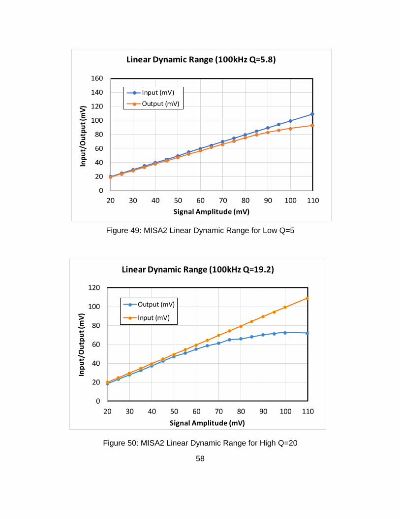
Linear Range ............................................................................................... 57 Matching Performance ................................................................................. 59
Chapter Five Conclusions ................................................................................... 70 Summary of Performance ............................................................................... 70 Discussion ....................................................................................................... 70
List of References ............................................................................................... 72
Vita ...................................................................................................................... 76
vii
LIST OF TABLES
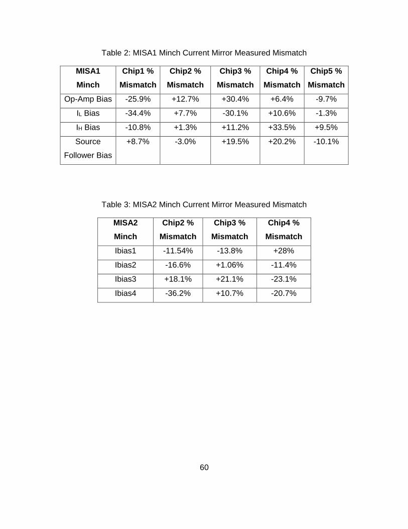
Table 1: Power Consumption of Biquad Filters across Frequency Spectrum ..... 54 Table 2: MISA1 Minch Current Mirror Measured Mismatch ................................ 60 Table 3: MISA2 Minch Current Mirror Measured Mismatch ................................ 60
viii
LIST OF FIGURES
Figure 1: Schematic and Transfer Function of the 2nd-Order OTA-C4 Filter (MISA1) ......................................................................................................... 4
Figure 2: MISA1 16th-Order Response at 6kHz and Multiple Harmonic Frequencies ................................................................................................... 6
Figure 3: MISA1 Demonstration System ............................................................... 6 Figure 4: LabVIEW GUI Screenshot for Running Demonstration ......................... 7 Figure 5: Maximum Theoretical Realized Q for Increasing Capacitance and Filter
Order ............................................................................................................. 9
Figure 6: Comparison of 2nd-, 4th-, 6th-, and 8th-Order Normalized Biquad Filter Responses for Various Q Values: Q=5 (Top Left), Q=10 (Top Right), Q=15 (Bottom Left) and Q=20 (Bottom Right) ....................................................... 10
Figure 7: Schematic of Ideal Biquad using Modeled Transconductors ............... 16
Figure 8: Swept Bias Current for Control of Filter Center Frequency .................. 16 Figure 9: Swept Bias Current for Control of Filter Q ............................................ 17 Figure 10: Schematic of Ideal Biquad with Modeled Output Resistance ............. 18
Figure 11: Filter Response with Decreasing Output Impedance ......................... 19 Figure 12: Schematic of Folded Cascode OTA ................................................... 23
Figure 13: OTA Closed-Loop Gain for 1nA Bias ................................................. 24 Figure 14: OTA Closed-Loop Gain for 100nA Bias ............................................. 24 Figure 15: OTA Open-Loop Gain and Phase for 1nA Bias ................................. 25
Figure 16: OTA Open-Loop Gain and Phase for 100nA Bias ............................. 25
Figure 17: Biquad Filter Topology and Transfer Function ................................... 28 Figure 18: Gm1 and Gm2 Current Bias Sweep Controlling Filter Center Frequency
Figure 19: Center Frequency Vs. Bias Current Relationship Trendlin................. 29 Figure 20: Gm3 Current Bias Sweep Controlling Filter Q ..................................... 30
Figure 21: Quality Factor Vs. Bias Current Relationship Trendline ..................... 30 Figure 22: Gm4 Current Bias Sweep Controlling Filter Gain ................................ 31
Figure 23: Gain Vs. Bias Current Relationship Trendline .................................... 31 Figure 24: Gm3 Bias Current Sweep Controlling Q and Phase Margin ................ 32 Figure 25: Minch Schematic ............................................................................... 33 Figure 26: Minch I-V Curve for Bias Currents of 1nA, 10nA, 100nA, and 1uA .... 34
Figure 27: Minch Current Gain Sweep ................................................................ 34 Figure 28: Op-Amp Schematic ............................................................................ 35 Figure 29: Op-Amp Closed-Loop Gain ................................................................ 36
Figure 30: OTA Open-Loop Gain and Phase ...................................................... 36 Figure 31: Schematic of Four Cascaded Biquad Filter Cells ............................... 37 Figure 32: Plot of Biquad Filter Bank with 2nd-, 4th-, 6th-, and 8th-Order Responses
..................................................................................................................... 38 Figure 33: Layout of MISA2 Chip ........................................................................ 40
ix
Figure 34: Monte Carlo Results of the Minch Current Mirror Mismatch Vs. Device Channel Length ........................................................................................... 41
Figure 40: Comparison of the Measured 2nd-, 4th-, 6th-, 8th-Order Biquad Filters and the MISA1 16th-Order Filter ................................................................... 49
Figure 41: Normal (Left) and Zoomed (Right) Views of the 8th-Order Biquad Filter and the MISA1 16th-Order Filter Measured Frequency Response ............... 49
Figure 47: MISA2 Measured THD Spectrum of Both 2nd- and 8th-Order Filters .. 56 Figure 48: THD Comparison between 2nd- and 8th-Order Response for Increasing
Figure 49: MISA2 Linear Dynamic Range for Low Q=5 ...................................... 58 Figure 50: MISA2 Linear Dynamic Range for High Q=20 ................................... 58
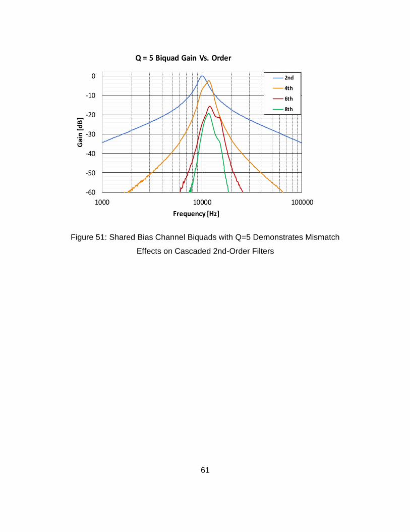
Figure 51: Shared Bias Channel Biquads with Q=5 Demonstrates Mismatch Effects on Cascaded 2nd-Order Filters ........................................................ 61
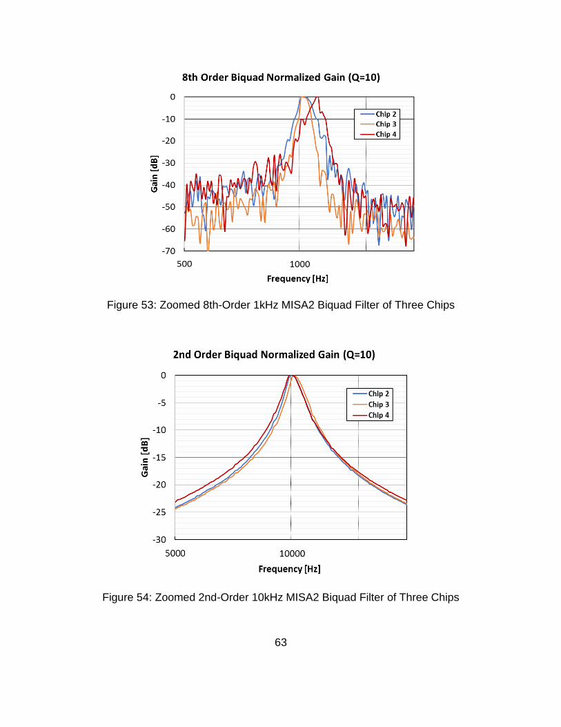
Figure 52: Zoomed 2nd-Order 1kHz MISA2 Biquad Filter of Three Chips .......... 62 Figure 53: Zoomed 8th-Order 1kHz MISA2 Biquad Filter of Three Chips ........... 63
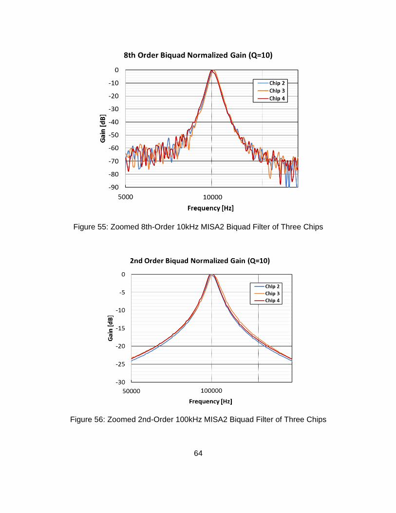
Figure 54: Zoomed 2nd-Order 10kHz MISA2 Biquad Filter of Three Chips ........ 63 Figure 55: Zoomed 8th-Order 10kHz MISA2 Biquad Filter of Three Chips ......... 64 Figure 56: Zoomed 2nd-Order 100kHz MISA2 Biquad Filter of Three Chips ...... 64
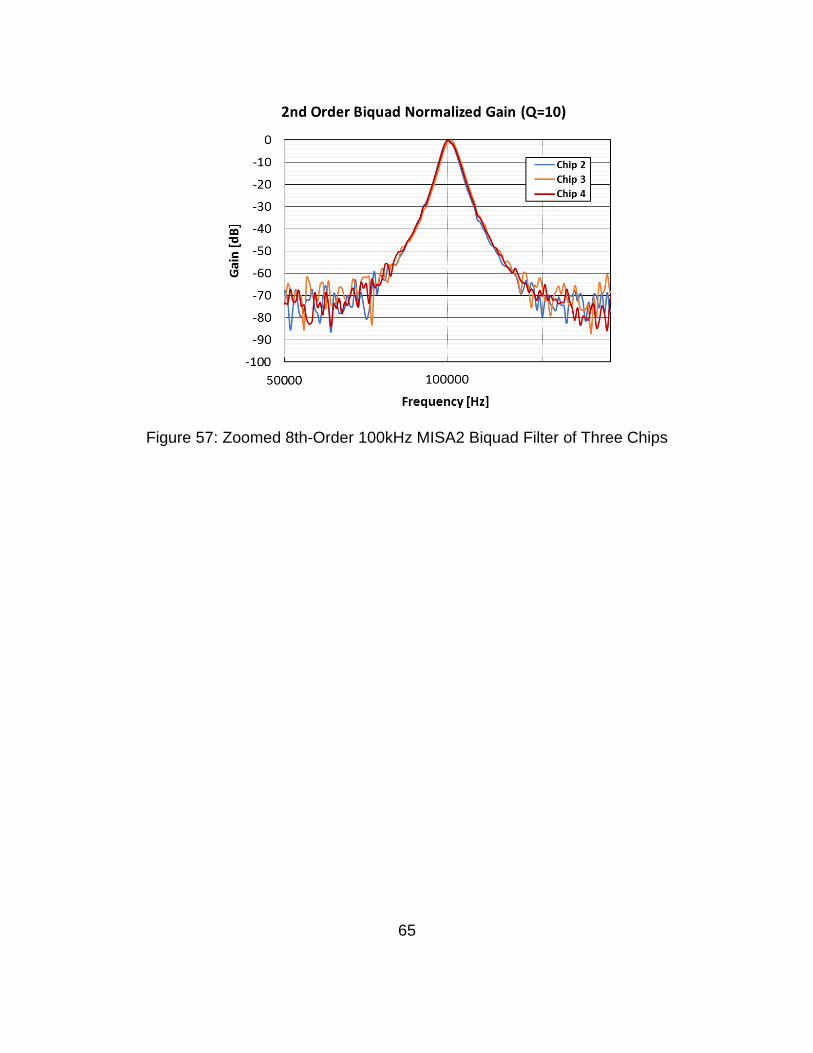
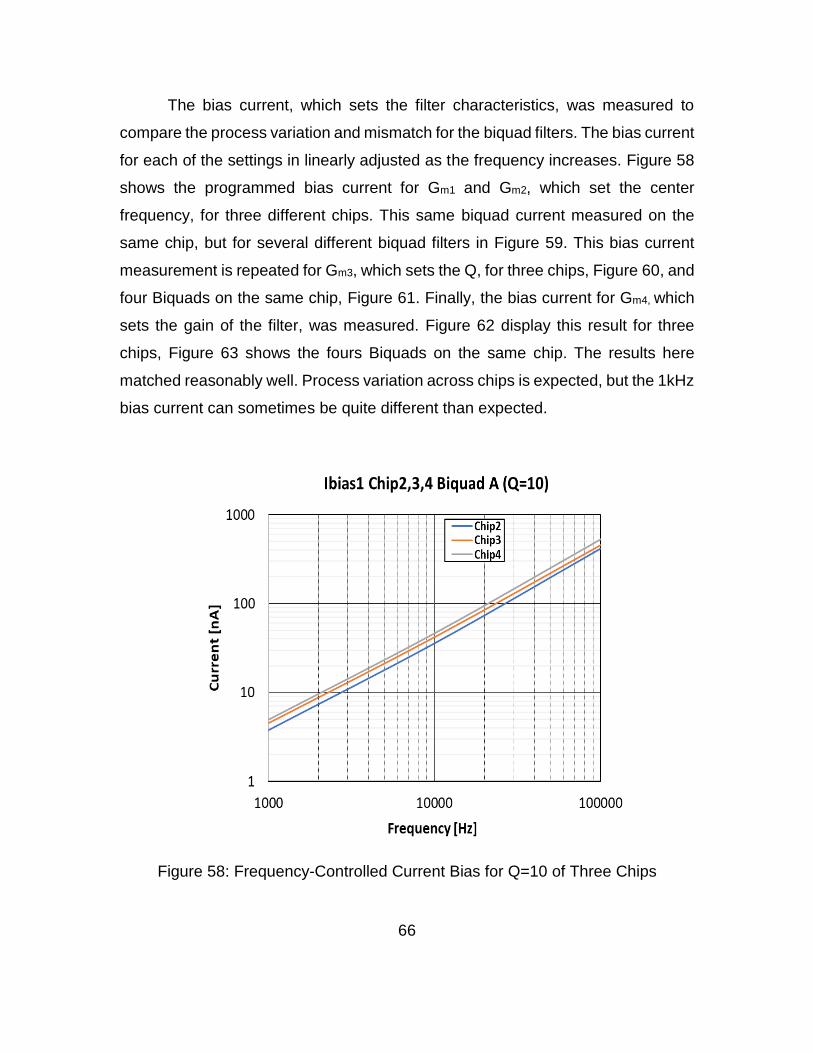
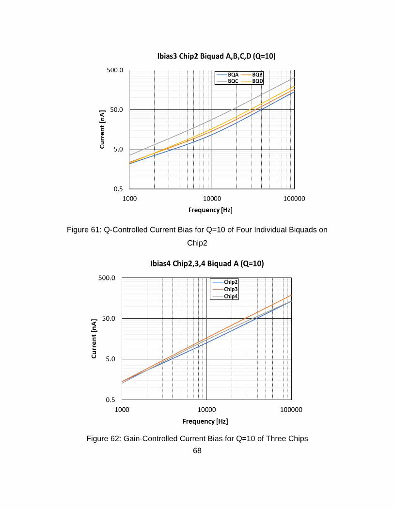
Figure 57: Zoomed 8th-Order 100kHz MISA2 Biquad Filter of Three Chips ....... 65 Figure 58: Frequency-Controlled Current Bias for Q=10 of Three Chips ............ 66
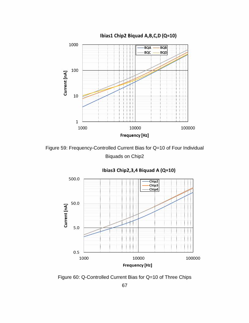
Figure 59: Frequency-Controlled Current Bias for Q=10 of Four Individual Biquads on Chip2 ........................................................................................ 67
Figure 60: Q-Controlled Current Bias for Q=10 of Three Chips .......................... 67 Figure 61: Q-Controlled Current Bias for Q=10 of Four Individual Biquads on
Figure 62: Gain-Controlled Current Bias for Q=10 of Three Chips ..................... 68
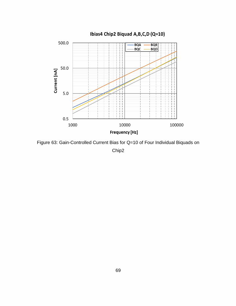
Figure 63: Gain-Controlled Current Bias for Q=10 of Four Individual Biquads on Chip2 ........................................................................................................... 69
1
CHAPTER ONE
INTRODUCTION
Motivation
Remote sensing networks is an evolving technology that has enabled the
realization of the Internet of Things (IoT), commonly defined as a network of
embedded, internet connected physical devices that interact and collect and
exchange data. There are numerous applications for the IoT across all technology
sectors including commercial, industrial, and government. Use in industrial
applications, such as the Smart Grid and power generation, may include platform
specialization to facilitate both system health monitoring and predictive
maintenance. Associated common methods include motor current and vibrational
analysis with an emphasis on identifying particular signal frequency components.
This work focuses on realizing a key hardware component for many of these
monitoring and/or control hardware platforms – a very low power, programmable
analog filter that will enable highly efficient signal signature analysis.
Objective
One of the challenges for a remote sensing platform is obtaining a balance
between very low power operation (enabling a long dwell time battery operated
sensor) and high-fidelity data processing (typically requiring large amounts of
power) for optimized signal detection. Digital Signal Processing (DSP) excels at
high performance data processing but can require excessive amounts of power, a
requirement not suitable for battery-powered remote sensing applications. Thus,
the primary objective of this research is to realize an Analog Signal Processing
2
(ASP) front-end that when coupled with a low-power microcontroller backend,
could provide sufficient performance to meet our platform goals: very low power
operation for extended dwell times, and sufficient sensitivity for limited signal
spectral analysis. For vibrational analysis, the ASP-based solution will need to
perform harmonic discrimination at multiple target frequencies. The ASP-based
programmable filter developed in this work will enable platforms capable of
performing very lower power, digitally controlled spectrum scanning and
discrimination.
3
CHAPTER TWO
BACKGROUND
Previous Work
The work presented in this thesis builds on the preceding research for a
similar project conducted by Ben Roehrs [1]. The purpose of this thesis is to
leverage the successes of the previous work, while improving the performance and
efficiency using a unique filter design. The prior research presented a Multi-
channel Integrated Spectrum Analyzer (MISA1) which utilized a monolithic, high-
order filter system with off-chip biasing and signal buffer circuits. The integrated
circuit consisted of two filter channels. Each channel was comprised of four
cascaded OTA-C4 [1] (Operational Transconductance Amplifier – Four
Capacitors) filters shown in Figure 1, with intermediate output buffers and Minch
current mirror biasing (not shown). Each OTA-C4 cell was designed to have a
fixed quality factor of ~2.1.
4
Figure 1: Schematic and Transfer Function of the 2nd-Order OTA-C4 Filter
(MISA1)
Results
The MISA1 chip can scan a spectral band of 2kHz [kilohertz] to >100kHz
with an ‘effective’ quality factor (Q) of 6, if configured as a 16th-order filter (eight
2nd-order C4-OTA cells in series). The measured transfer function for this MISA1
filter configuration is plotted in Figure 2 for six different center frequencies. A test
system was developed and built to demonstrate the functionality of the chip with
PC-based programmability of the filter functions for automated spectral analysis
(see Figure 3). This was completed using a custom printed circuit board (PCB)
incorporating an SPI (Serial Peripheral Interface) port for programming the DACs
(Digital-to-Analog Convertors), enabling digital control of the MISA1 filter center
frequency via bias current programming. A MISA1 control and spectral analysis
program displayed in Figure 4 was created using LabVIEW and an Agilent multi-
function data acquisition module (Agilent U2531A, 4 Channel, Simultaneous
5
Sampling, 14 Bits, 2MS/s) used to provide both digital control and signal
digitization. With the system complete, a full demonstration was conducted using
representative sensor signals and the analysis results indicated successful
classification of a signature of harmonic signals. The MISA1 tests demonstrated
the feasibility for very low power detection of the target signals and supported the
premise for a highly miniaturized, very low power signal signature analysis system
based on the MISA1 chip.
6
Figure 2: MISA1 16th-Order Response at 6kHz and Multiple Harmonic
Frequencies
Figure 3: MISA1 Demonstration System
7
Figure 4: LabVIEW GUI Screenshot for Running Demonstration
8
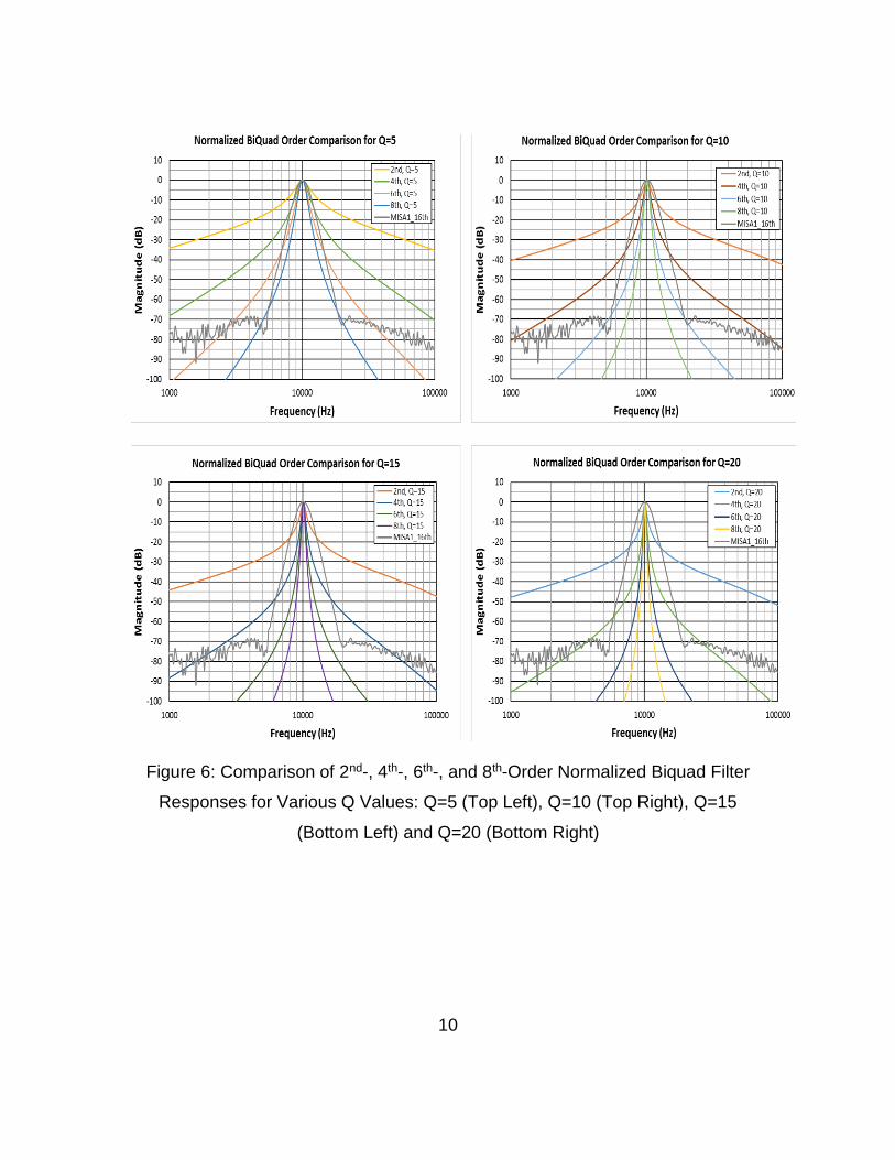
Improvements
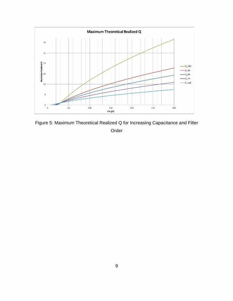
While the original MISA1 chip performed well, further improvements in
system operation through increased spectral selectivity are possible by increasing
the quality factor (Q) of the filter transfer function. Methods for improving the overall
filter Q were investigated beginning with a re-evaluation of the MISA filter topology
for maximizing Q. However, the MISA1 topology would require use of a very large
integrated capacitance and a very well matched high-order filter cascade to
accomplish this, as demonstrated in Figure 5 for the ideal circuit. The use of a
super heterodyne mixer and low-pass filter architecture was also investigated
since it is common in higher end spectrum analyzers. However, the requirement
for a tunable, low distortion reference signal and its associated power consumption
made this topology undesirable. In addition, other filter designs having much
increased Q were simulated in SPICE including topologies based on gyrator-C
active filters and biquadratic active filters with variable Q adjustment. This
investigation (see Figure 6) shows the theoretical range of filter performance
possible. Each plot illustrates the filter response for increasing filter order for a
fixed quality factor. From the top left plot to the bottom right plot the fixed Q is
increased to demonstrate the response differences from the filter order. These
plots are continually compared to the MISA1 measurements of the 16th-order
response to justify the needed improvements for the filter design.
9
Figure 5: Maximum Theoretical Realized Q for Increasing Capacitance and Filter
Order
10
Figure 6: Comparison of 2nd-, 4th-, 6th-, and 8th-Order Normalized Biquad Filter
Responses for Various Q Values: Q=5 (Top Left), Q=10 (Top Right), Q=15
(Bottom Left) and Q=20 (Bottom Right)
11
Literature Review
Initially, a wide array of books and publications were studied for background
information on analog filter design. This was carried out to refresh the basics of
circuit analysis for complex transfer functions, to develop a sense of practical
design from common techniques demonstrated in literature, and to review the
diversity of solutions available to direct efforts towards more promising filter
architectures. Thus, multiple techniques for highly selective filter were evaluated
including the following: analog active filter banks, active inductor or gyrator-C
topologies, biquadratic active filters, and Gm-C filters. Eventually, the final design
would implement several features of these different techniques in order to utilize
the advantages offered by each for constructing a robust filter design.
References on Filters
The Gm-C filter [2] can be the basis for many of these techniques, although
it is not always required. This topology consists of at least one transconductor and
one capacitor. In its simplest form a series combination produces a low-pass filter,
while a parallel combination produces a high-pass filter. What stands out is the
transconductor, which can be tuned to a specific value using a bias current, as
often utilized in an OTA (operational tranconductance amplifier). These Gm-C
filters are the building blocks for various filter responses and are implemented
readily from a desired transfer function. The simple derivation of a Gm-C filter is
also very appealing, because a desired transfer function can be used to rapidly
generate a filter topology.
The primary reference for the MISA1 filter was a low-power high-order
analog filter bank presented by Graham et al. in [3] and [4]. This technique took
advantage of cascaded filters to achieve a higher performance filter with minimal
power consumption of each cell. While it also included floating gate transistors for
a low-power bias network, this was not implemented in our previous work due the
12
complexity of programming floating gates. However, this approach is limited in the
spectral selectivity that is practically obtainable, since very large capacitors and/or
very high filter order would be necessary to achieve the desired response for our
application.
The active inductor, also known as the gyrator-C, is a filter topology that can
produce very high spectral selectivity using minimal stages, with a reasonable
capacitance spread. Using this architecture Sundarasrandula et el. [6]
demonstrated a 1-V, 6nW programmable 4th-order filter that achieved a quality
factor, Q, of up to 50. This technique was also implemented by Duan et al. [7] for
a high Q band-pass filter at 46MHz. However, this topology is susceptible to
stability issues as any high Q circuits would also encounter. Thus, this type of
design must consider precision and matching of circuit components to ensure
stability during operation.
Biquadratic filters offer a flexible architecture with independent control over
filter characteristics. A biquadratic topology can be generated from a desired
transfer function, which allows simple modifications to a circuit topology without
complex derivations for the new transfer functions. One example of this
architecture is given by Geiger et al. [5]. With the ability to tune circuit components
independently, the filter characteristics can be swept, remain constant, or act as a
function of another characteristic. For instance, the Q of a biquadratic filter can be
set to linearly increase with the center frequency. These advantages of the
biquadratic transfer function make it an appealing approach for tunable filter
designs.
13
CHAPTER THREE
DESIGN DEVELOPMENT
Specifications and Requirements
In order to begin the formal design process, a set of specifications and
requirements were necessary to narrow the design choices. The primary
specifications include the following: programming of the filter center frequency from
1kHz-100kHz, programming of the filter selectivity (or Q) with the minimum Q of
10, programming of the filter cell gain ( 3dB) to maintain an overall filter channel
gain of approximately 0dB, and minimal power consumption at or below the 155µW
measured for MISA1, while maintaining the above specifications. Secondary
requirements included the following: maximized linear dynamic range to maximize
the filter SNR with a fixed noise floor, the ability to cascade the 2nd order filter
sections to obtain higher order filter responses, and the ability to observe each
filter output signal.
Filter Characteristics
With the general specifications of the filter channel determined, the
characteristics of the band-pass filter cell could be derived. The ideal 2nd-order
transfer function, shown in Equation 1, could be examined for the primary
components that established the filter response. The center frequency, 𝑓𝑜, of the
band-pass response is determined by the term 𝜔𝑜 = 𝑓𝑜
2𝜋, and will be determined by
the two poles and the zero. The 3dB bandwidth of the filter, 𝜔𝑜
𝑄, sets the 3dB-width
of the passband of the band-pass filter. The center frequency divided by the 3dB
bandwidth gives the quality factor, Q, of the filter which is a unit-less term that can
be compared across the spectrum. Finally, the gain of the filter, 𝐻𝑜, is the output-
14
to-input signal gain at the peak of the passband function. These characteristics
can be equated to the requirements for the frequency range, 1kHz-100kHz, and
the quality factor, greater than or equal to 10.
𝐻(𝑠) = 𝐻𝑜
𝜔𝑜
𝑄 𝑠
𝑠2 +𝜔𝑜
𝑄 𝑠 + 𝜔𝑜2
𝐸𝑞. (1)
Design Methodology
System Architecture
Candidate system architectures were explored and compared in terms of
the functional advantages, disadvantages, and practicality of implementation. A
filter bank architecture has proven beneficial for increasing performance of a single
2nd-order filter cell, but without significant improvement over the MISA1 design
would require too many resources to obtain the desired spectral selectivity.
Consequently, significant improvement in the narrowband characteristics of the
base 2nd-order filter cell (higher Q) was targeted, which would enable much
improved spectral selectivity, using significantly fewer cascaded stages than
required using the MISA1 design. The combination of Gm-C high-pass and low-
pass filters has proven to obtain a limited quality factor. The active inductor or
gyrator-C circuit can acquire a very narrowband response for a 2nd-order system
but can lead to an unstable filter if not properly implemented. So, a method
enabling fine control of the Q, and therefore the stability of filter, was determined
essential. From the previous filter topology review, Gm-C based filters provide the
ability for fine Q control. Gm-C cells can easily be configured to implement a wide
range of transfer functions, but also allow a specific circuit component to be
modified with the bias current of the transconductor. Thus, the Gm-C network was
15
selected for implementing desired filter characteristics, including control of the filter
center frequency and quality factor.
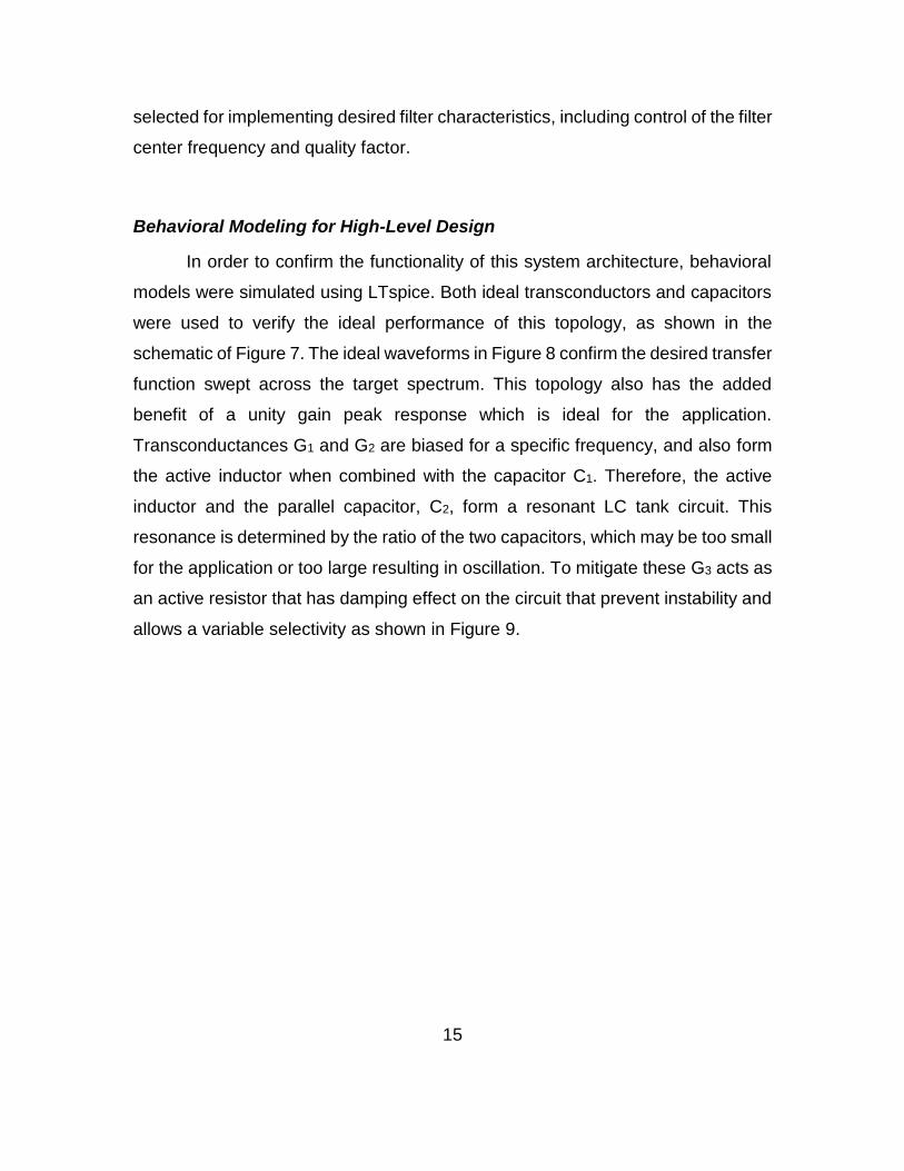
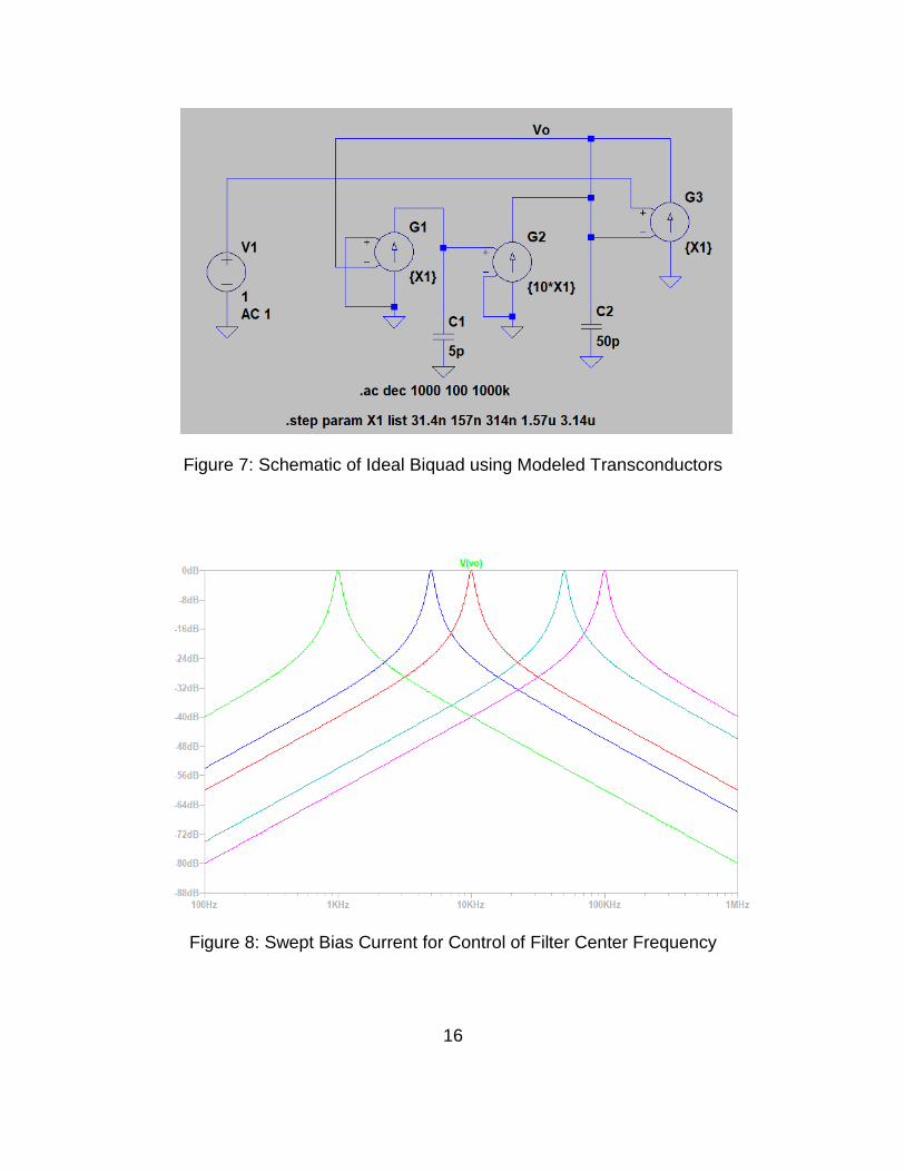
Behavioral Modeling for High-Level Design
In order to confirm the functionality of this system architecture, behavioral
models were simulated using LTspice. Both ideal transconductors and capacitors
were used to verify the ideal performance of this topology, as shown in the
schematic of Figure 7. The ideal waveforms in Figure 8 confirm the desired transfer
function swept across the target spectrum. This topology also has the added
benefit of a unity gain peak response which is ideal for the application.
Transconductances G1 and G2 are biased for a specific frequency, and also form
the active inductor when combined with the capacitor C1. Therefore, the active
inductor and the parallel capacitor, C2, form a resonant LC tank circuit. This
resonance is determined by the ratio of the two capacitors, which may be too small
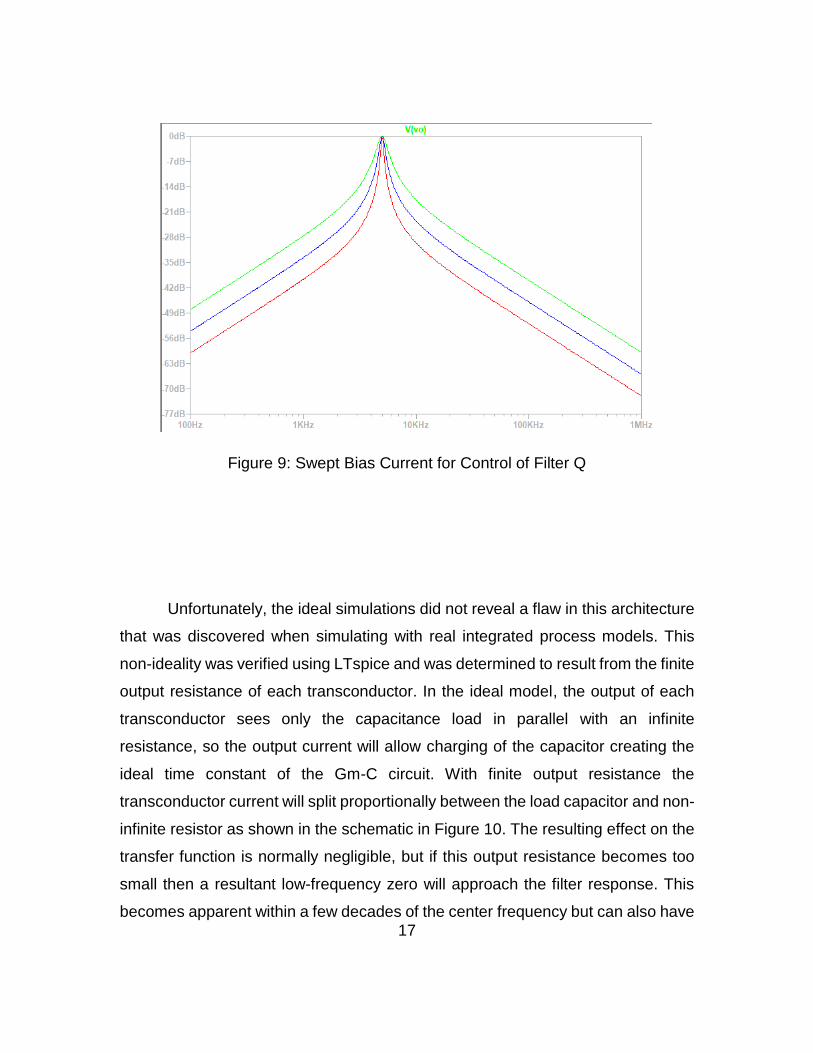
for the application or too large resulting in oscillation. To mitigate these G3 acts as
an active resistor that has damping effect on the circuit that prevent instability and
allows a variable selectivity as shown in Figure 9.
16
Figure 7: Schematic of Ideal Biquad using Modeled Transconductors
Figure 8: Swept Bias Current for Control of Filter Center Frequency
17
Figure 9: Swept Bias Current for Control of Filter Q
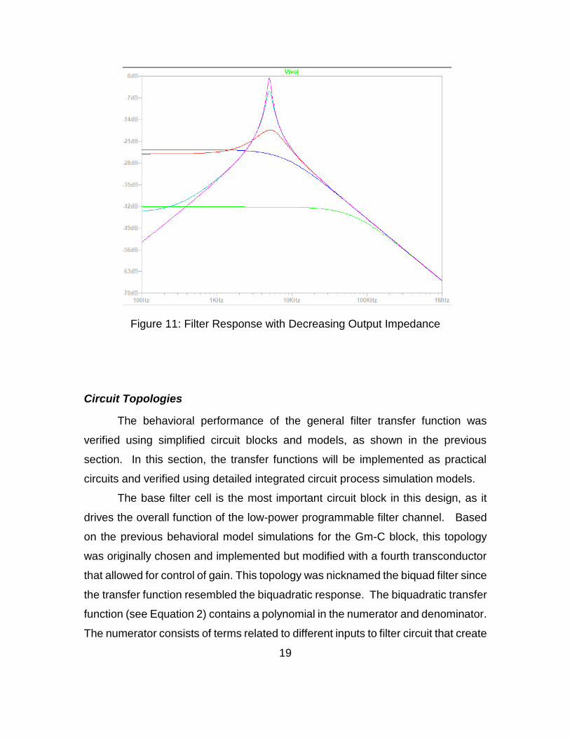
Unfortunately, the ideal simulations did not reveal a flaw in this architecture
that was discovered when simulating with real integrated process models. This
non-ideality was verified using LTspice and was determined to result from the finite
output resistance of each transconductor. In the ideal model, the output of each
transconductor sees only the capacitance load in parallel with an infinite
resistance, so the output current will allow charging of the capacitor creating the
ideal time constant of the Gm-C circuit. With finite output resistance the
transconductor current will split proportionally between the load capacitor and non-
infinite resistor as shown in the schematic in Figure 10. The resulting effect on the
transfer function is normally negligible, but if this output resistance becomes too
small then a resultant low-frequency zero will approach the filter response. This
becomes apparent within a few decades of the center frequency but can also have
18
a detrimental effect on the filter response if the output resistance becomes
comparable to transconductors as shown in Figure 11. This non-ideality will be
considered in the low-level design of the transconductors themselves. This effect
also contributes to non-ideal gain of the transfer function, which requires an extra
transconductor to maintain a unity gain response.
Figure 10: Schematic of Ideal Biquad with Modeled Output Resistance
19
Figure 11: Filter Response with Decreasing Output Impedance
Circuit Topologies
The behavioral performance of the general filter transfer function was
verified using simplified circuit blocks and models, as shown in the previous
section. In this section, the transfer functions will be implemented as practical
circuits and verified using detailed integrated circuit process simulation models.
The base filter cell is the most important circuit block in this design, as it
drives the overall function of the low-power programmable filter channel. Based
on the previous behavioral model simulations for the Gm-C block, this topology
was originally chosen and implemented but modified with a fourth transconductor
that allowed for control of gain. This topology was nicknamed the biquad filter since
the transfer function resembled the biquadratic response. The biquadratic transfer
function (see Equation 2) contains a polynomial in the numerator and denominator.
The numerator consists of terms related to different inputs to filter circuit that create
20
a high-pass, band-pass and low-pass functions: 𝑉𝐻𝑃𝑠2 + 𝑉𝐵𝑃𝑠 + 𝑉𝐿𝑃. In this case,
the high-pass and low-pass inputs are grounded and reduce to the equation to the
generic band-pass function as seen in Equation 1.
𝐻(𝑠) = 𝑉𝐻𝑃𝑠2 + 𝑉𝐵𝑃𝑠 + 𝑉𝐿𝑃
𝑠2 +𝜔𝑜
𝑄 𝑠 + 𝜔𝑜2
𝐸𝑞. (2)
As discussed in the previous section this topology required robust
transconductors to mitigate the effect of finite output impedance. Each
transconductor would also need to be variable to control each of the filter’s
characteristics. Therefore, an operational transconductance amplifier (OTA) was
chosen with a current biased differential pair and a folded cascode output stage
for much higher output impedance. The linearity of these transconductors was a
major concern since this would limit the input signal size allowed to maintain
linearity and small-signal assumptions. A bump differential pair was added for a
boost to the OTA linearity.
Along with the main biquad filter cell, two other circuits were needed: the
buffer located between cascaded filter cells, and the biasing scheme for the
variable OTA’s. The buffers were chosen to be robust operational amplifiers (Op-
Amps) in unity gain configuration using negative feedback. The Op-Amp topology
was designed as a current biased differential pair with Class AB output stage and
added compensation for adequate bandwidth and stability. The biasing scheme,
based on the circuit introduced by Minch [8], was designed as a high input and
output resistance current mirror that maintains saturation throughout a very wide
current range. Using these components, a filter bank channel will be constructed
composed of four biquad filter cells, an Op-Amp buffering between stage, and at
least five Minch current mirrors composed of the bias currents for the biquad filter
cell and Op-Amp buffer. In the final filter channel implementation, the current
21
mirrors will be digitally programmed off-chip for control of each filter cell’s gain,
quality factor, and center frequency.
Technology Current Extraction
The sizing of the transistors used in the OTA depends on three major points.
First, the required frequencies and capacitors implemented determine the
necessary transconductance for each filter’s characteristics. Second, the inversion
coefficient for each device sets the relationship between bias current and
transconductance. In the subthreshold region, or weak inversion,
transconductance is related linearly with bias current and is also the most power-
efficient mode of operation. Third, the length of each will be optimized using longer
channel lengths for best matching against short-channel effects and process
variation; while also reducing channel length for parasitic capacitance that reduce
bandwidth.
𝐼𝑛𝑣𝑒𝑟𝑠𝑖𝑜𝑛 𝐶𝑜𝑒𝑓𝑓𝑖𝑐𝑒𝑛𝑡 [𝐼𝐶] =𝐼𝐷
2𝑛𝜇𝐶𝑂𝑋′ 𝑈𝑇
2 𝑊𝐿
=𝐼𝐷
𝐼0𝑊𝐿
𝐸𝑞. (3)
𝑊𝑒𝑎𝑘 𝐼𝑛𝑣𝑒𝑟𝑠𝑖𝑜𝑛: 𝐼𝐶 ≤ 0.1
𝑀𝑜𝑑𝑒𝑟𝑎𝑡𝑒 𝐼𝑛𝑣𝑒𝑟𝑠𝑖𝑜𝑛: 0.1 < 𝐼𝐶 < 10
𝑆𝑡𝑟𝑜𝑛𝑔 𝐼𝑛𝑣𝑒𝑟𝑠𝑖𝑜𝑛: 𝐼𝐶 ≤ 10
The inversion coefficient describes the three biasing schemes of a saturated
transistor. Equation 3 shows the expression for the inversion coefficient and lists
the three different types of inversion modes: weak, moderate, and strong as
derived from Binkley [9]. Weak inversion is where the channel is barely inverted,
the gate-source voltage is below the threshold voltage of the device, and the
transconductance is linear with current. This regime generally has the lowest
values of transconductance and high power efficiency. Strong inversion where the
channel is fully inverted, the gate-source voltage is well above the threshold
22
voltage of the device, the transconductance is a square root function of current,
and generally has the highest values of transconductance with poor power
efficiency. Moderate inversion is the transitional period between them and is not
simply described with a single equation but produces a balance of
transconductance and power efficiency. The transistors were designed to operate
in the weak inversion region throughout the frequency range. Therefore, the
devices were sizes so that they would remain in weak inversion above 100kHz
with some margin for error. This was verified with a sized transistor and current
sweep simulation.
Simulation
Simulation of the chosen circuit topologies were conducted using
Cadence’s Virtuoso Analog Design Environment (ADE). All simulations were
performed using foundry provided process development kit (PDK) device models.
Note that the following simulation plots represent models from any generic
standard 1.8V core, 180nm process and do not represent any specific integrated
circuit fabrication process or foundry.
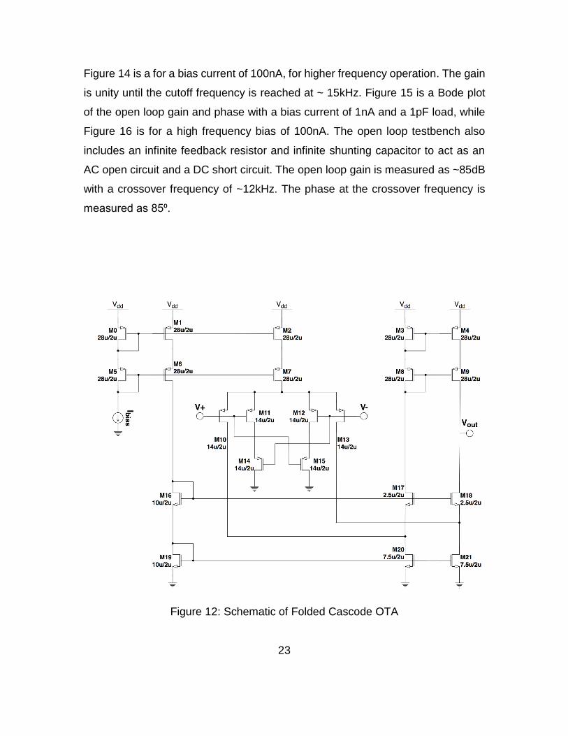
Operational Transconductance Amplifier
The topology implemented for the OTA is a current biased differential pair
with a bump degeneration and a folded cascode output stage. Figure 12 shows
the Cadence schematic for the OTA cell. The input bias current is mirrored with a
PMOS cascode to an output biasing branch and the source of the PMOS
differential input pair. The four transistor bump degeneration acts as cross-
coupled, source degeneration resistors. The output of the differential pair is fed to
the high impedance folded cascode output stage.
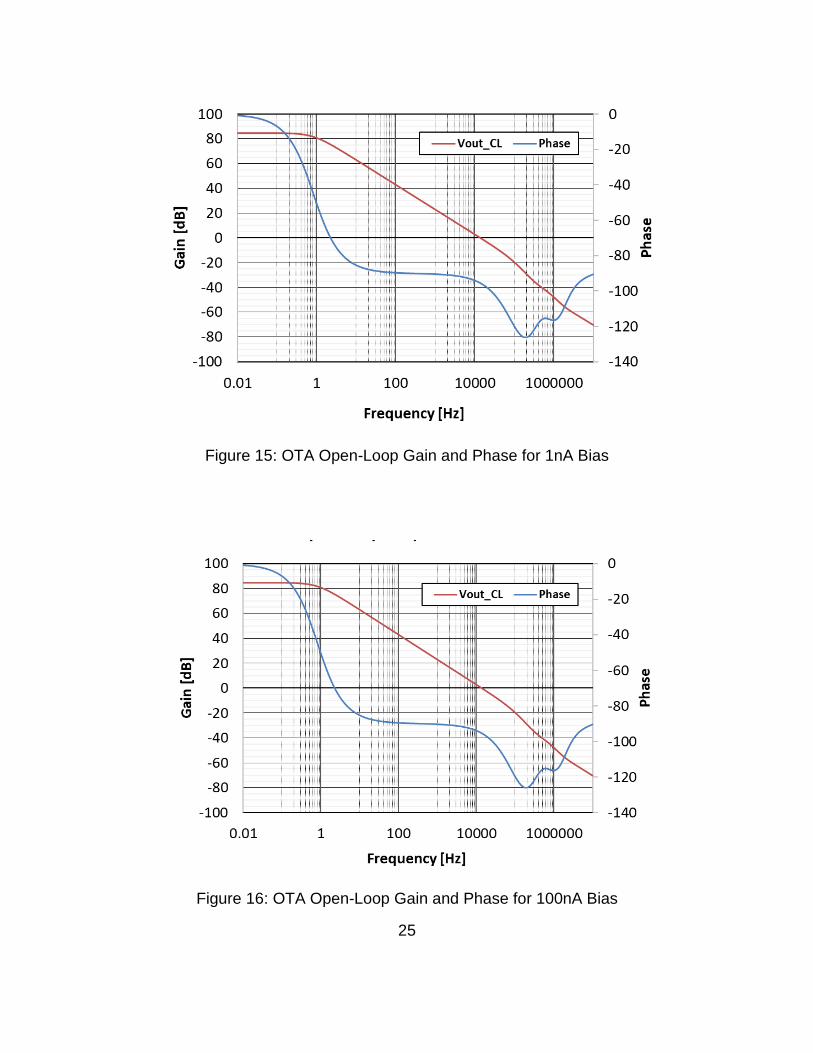
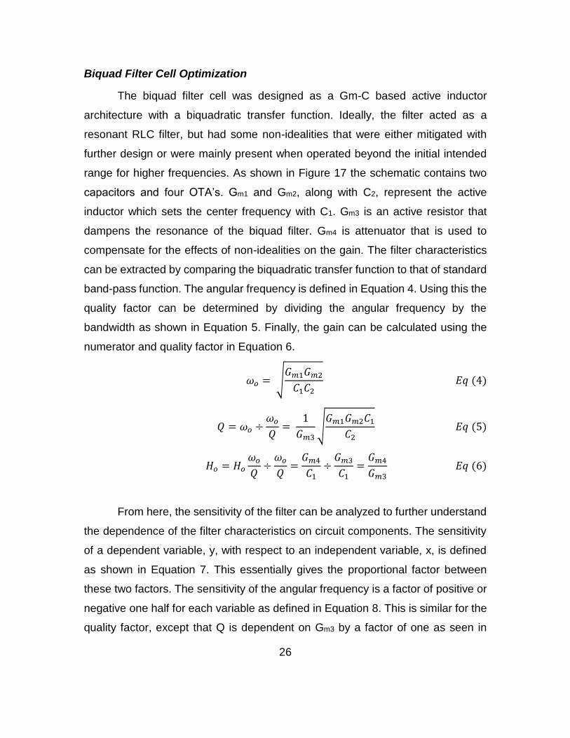
Simulations verified the expected performance of the OTA. Figure 13 shows a
Bode plot of the closed loop gain with a bias current of 1nA and a 1pF load, while
23
Figure 14 is a for a bias current of 100nA, for higher frequency operation. The gain
is unity until the cutoff frequency is reached at ~ 15kHz. Figure 15 is a Bode plot
of the open loop gain and phase with a bias current of 1nA and a 1pF load, while
Figure 16 is for a high frequency bias of 100nA. The open loop testbench also
includes an infinite feedback resistor and infinite shunting capacitor to act as an
AC open circuit and a DC short circuit. The open loop gain is measured as ~85dB
with a crossover frequency of ~12kHz. The phase at the crossover frequency is
measured as 85⁰.
Figure 12: Schematic of Folded Cascode OTA
24
Figure 13: OTA Closed-Loop Gain for 1nA Bias
Figure 14: OTA Closed-Loop Gain for 100nA Bias
25
Figure 15: OTA Open-Loop Gain and Phase for 1nA Bias
Figure 16: OTA Open-Loop Gain and Phase for 100nA Bias
26
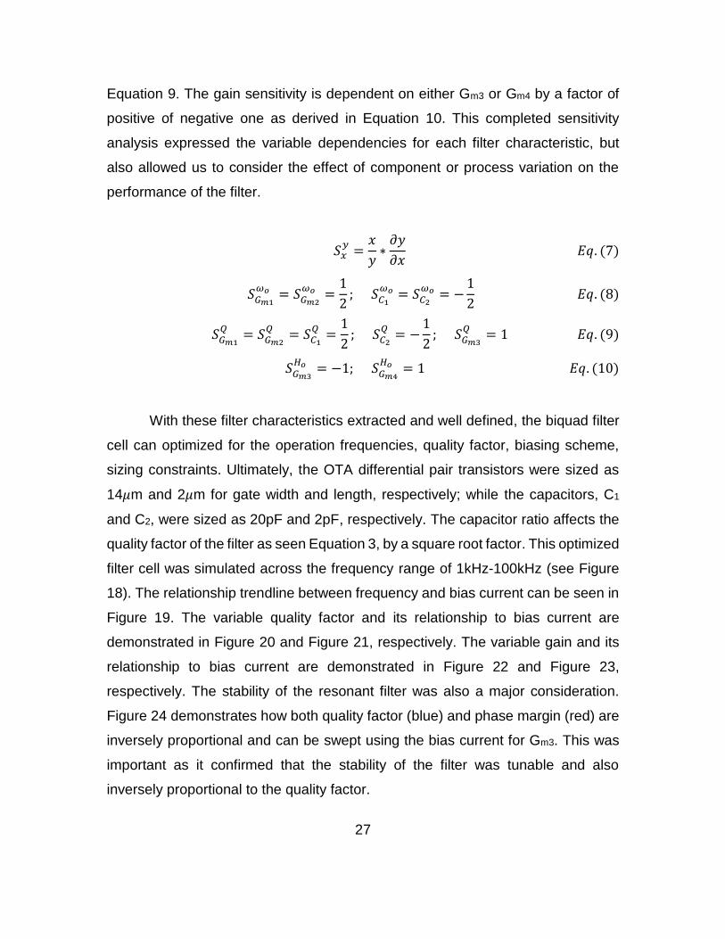
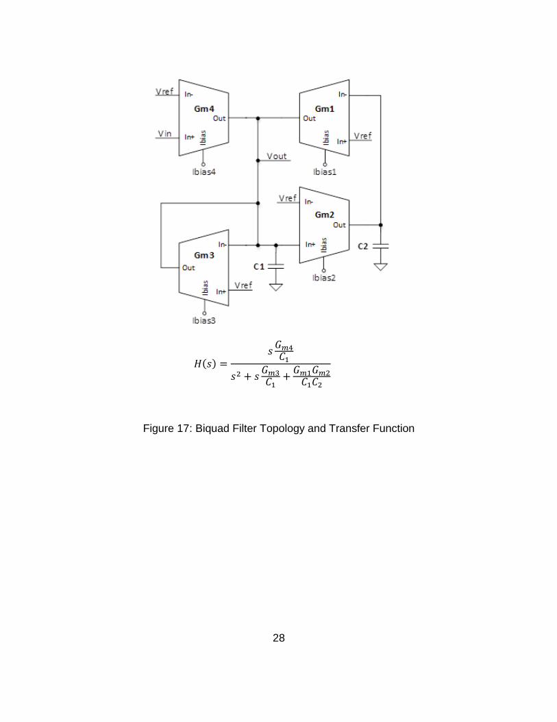
Biquad Filter Cell Optimization
The biquad filter cell was designed as a Gm-C based active inductor
architecture with a biquadratic transfer function. Ideally, the filter acted as a
resonant RLC filter, but had some non-idealities that were either mitigated with
further design or were mainly present when operated beyond the initial intended
range for higher frequencies. As shown in Figure 17 the schematic contains two
capacitors and four OTA’s. Gm1 and Gm2, along with C2, represent the active
inductor which sets the center frequency with C1. Gm3 is an active resistor that
dampens the resonance of the biquad filter. Gm4 is attenuator that is used to
compensate for the effects of non-idealities on the gain. The filter characteristics
can be extracted by comparing the biquadratic transfer function to that of standard
band-pass function. The angular frequency is defined in Equation 4. Using this the
quality factor can be determined by dividing the angular frequency by the
bandwidth as shown in Equation 5. Finally, the gain can be calculated using the
numerator and quality factor in Equation 6.
𝜔𝑜 = √𝐺𝑚1𝐺𝑚2
𝐶1𝐶2 𝐸𝑞 (4)
𝑄 = 𝜔𝑜 ÷𝜔𝑜
𝑄=
1
𝐺𝑚3
√𝐺𝑚1𝐺𝑚2𝐶1
𝐶2 𝐸𝑞 (5)
𝐻𝑜 = 𝐻𝑜
𝜔𝑜
𝑄÷
𝜔𝑜
𝑄=
𝐺𝑚4
𝐶1÷
𝐺𝑚3
𝐶1=
𝐺𝑚4
𝐺𝑚3 𝐸𝑞 (6)
From here, the sensitivity of the filter can be analyzed to further understand
the dependence of the filter characteristics on circuit components. The sensitivity
of a dependent variable, y, with respect to an independent variable, x, is defined
as shown in Equation 7. This essentially gives the proportional factor between
these two factors. The sensitivity of the angular frequency is a factor of positive or
negative one half for each variable as defined in Equation 8. This is similar for the
quality factor, except that Q is dependent on Gm3 by a factor of one as seen in
27
Equation 9. The gain sensitivity is dependent on either Gm3 or Gm4 by a factor of
positive of negative one as derived in Equation 10. This completed sensitivity
analysis expressed the variable dependencies for each filter characteristic, but
also allowed us to consider the effect of component or process variation on the
performance of the filter.
𝑆𝑥𝑦
=𝑥
𝑦∗
𝜕𝑦
𝜕𝑥 𝐸𝑞. (7)
𝑆𝐺𝑚1
𝜔𝑜 = 𝑆𝐺𝑚2
𝜔𝑜 =1
2; 𝑆𝐶1
𝜔𝑜 = 𝑆𝐶2
𝜔𝑜 = −1
2 𝐸𝑞. (8)
𝑆𝐺𝑚1
𝑄 = 𝑆𝐺𝑚2
𝑄 = 𝑆𝐶1
𝑄 =1
2; 𝑆𝐶2
𝑄 = −1
2; 𝑆𝐺𝑚3
𝑄 = 1 𝐸𝑞. (9)
𝑆𝐺𝑚3
𝐻𝑜 = −1; 𝑆𝐺𝑚4
𝐻𝑜 = 1 𝐸𝑞. (10)
With these filter characteristics extracted and well defined, the biquad filter
cell can optimized for the operation frequencies, quality factor, biasing scheme,
sizing constraints. Ultimately, the OTA differential pair transistors were sized as
14𝜇m and 2𝜇m for gate width and length, respectively; while the capacitors, C1
and C2, were sized as 20pF and 2pF, respectively. The capacitor ratio affects the
quality factor of the filter as seen Equation 3, by a square root factor. This optimized
filter cell was simulated across the frequency range of 1kHz-100kHz (see Figure
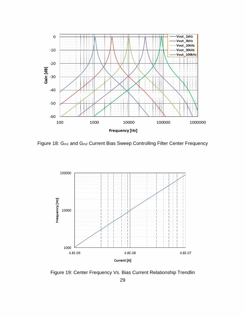
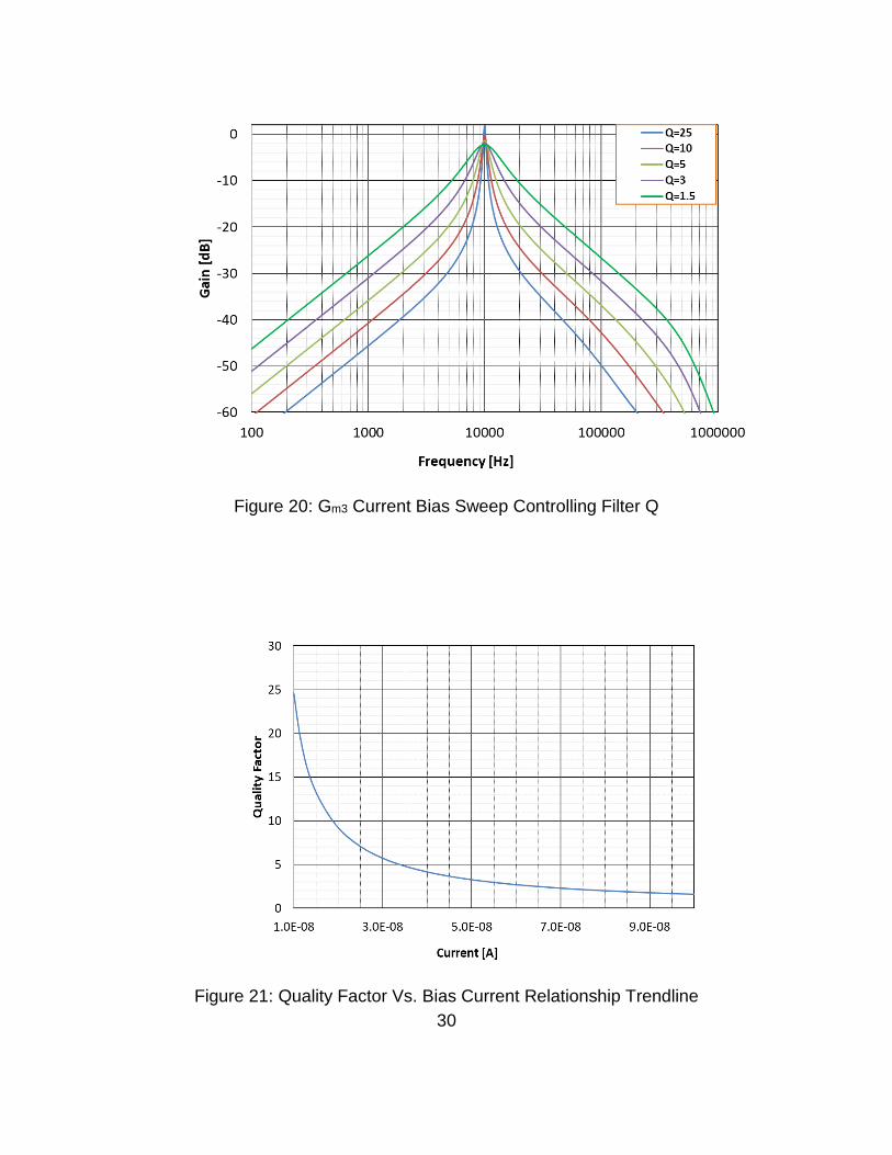
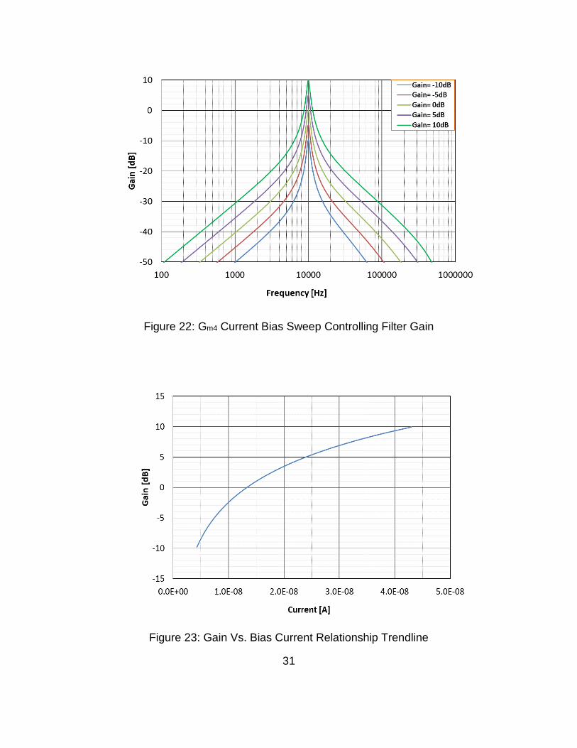
18). The relationship trendline between frequency and bias current can be seen in
Figure 19. The variable quality factor and its relationship to bias current are
demonstrated in Figure 20 and Figure 21, respectively. The variable gain and its
relationship to bias current are demonstrated in Figure 22 and Figure 23,
respectively. The stability of the resonant filter was also a major consideration.
Figure 24 demonstrates how both quality factor (blue) and phase margin (red) are
inversely proportional and can be swept using the bias current for Gm3. This was
important as it confirmed that the stability of the filter was tunable and also
inversely proportional to the quality factor.
28
Figure 17: Biquad Filter Topology and Transfer Function
𝐻(𝑠) =𝑠
𝐺𝑚4
𝐶1
𝑠2 + 𝑠𝐺𝑚3
𝐶1+
𝐺𝑚1𝐺𝑚2
𝐶1𝐶2
29
Figure 18: Gm1 and Gm2 Current Bias Sweep Controlling Filter Center Frequency
Figure 19: Center Frequency Vs. Bias Current Relationship Trendlin
30
Figure 20: Gm3 Current Bias Sweep Controlling Filter Q
Figure 21: Quality Factor Vs. Bias Current Relationship Trendline
31
Figure 22: Gm4 Current Bias Sweep Controlling Filter Gain
Figure 23: Gain Vs. Bias Current Relationship Trendline
32
Figure 24: Gm3 Bias Current Sweep Controlling Q and Phase Margin
Bias and Buffer Verification
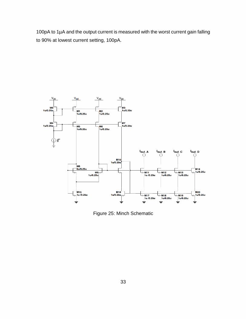
Both the Minch current mirror and the Op-Amp buffer were simulated and
verified for expected performance. The Minch current mirror schematic is
illustrated below in Figure 25. The Minch current mirror [10] was chosen because
of its optimal performance across a wide range of current levels including in the
subthreshold region. The input stage of the mirror is a simple PMOS cascode
current mirror that biases the rest of the circuit. Transistor M8 is sized much larger
than the unit transistors because it acts as current-controlled voltage source that
biases both M9 and M15 well above the saturation knee which is measured at
about 100mV. From here M10 and M16 act like a Sooch current mirror [11] that
replicate the saturation biasing to the output transistors. The current-voltage curve
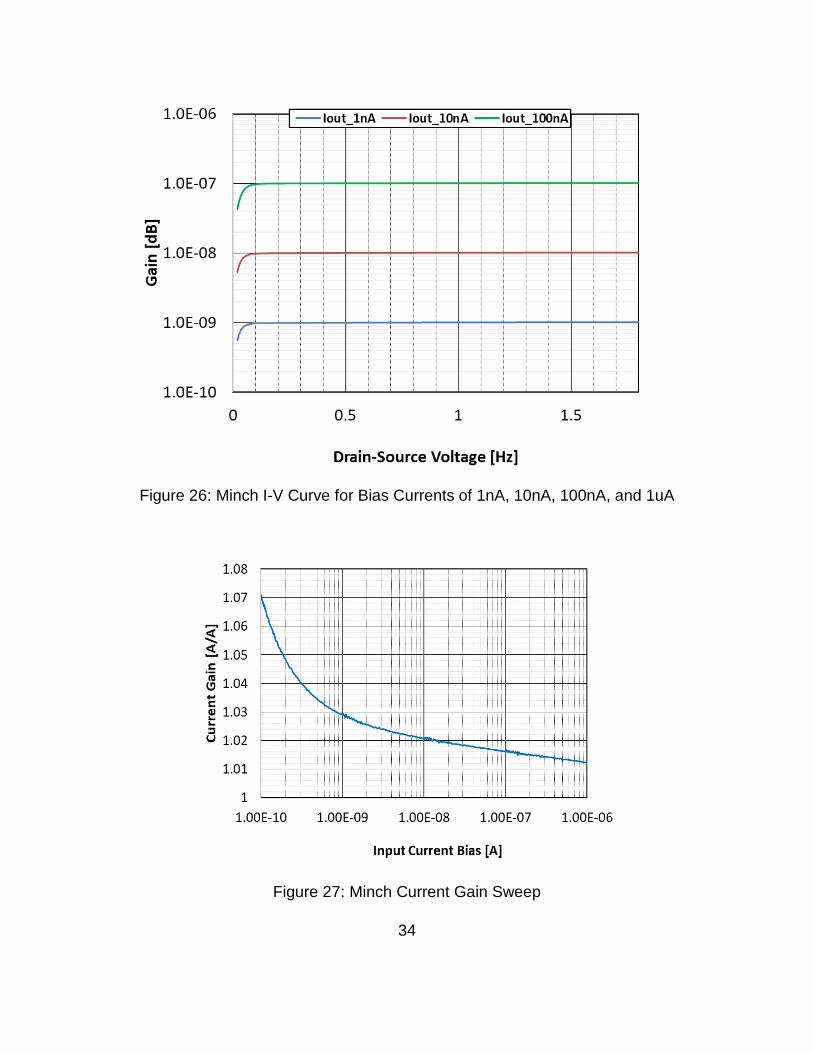
is plotted in Figure 26 with decreasing bias currents: 100nA, 10nA, and 1nA. The
current gain is also displayed in Figure 27 where the input current is swept from
33
100pA to 1µA and the output current is measured with the worst current gain falling
to 90% at lowest current setting, 100pA.
Figure 25: Minch Schematic
34
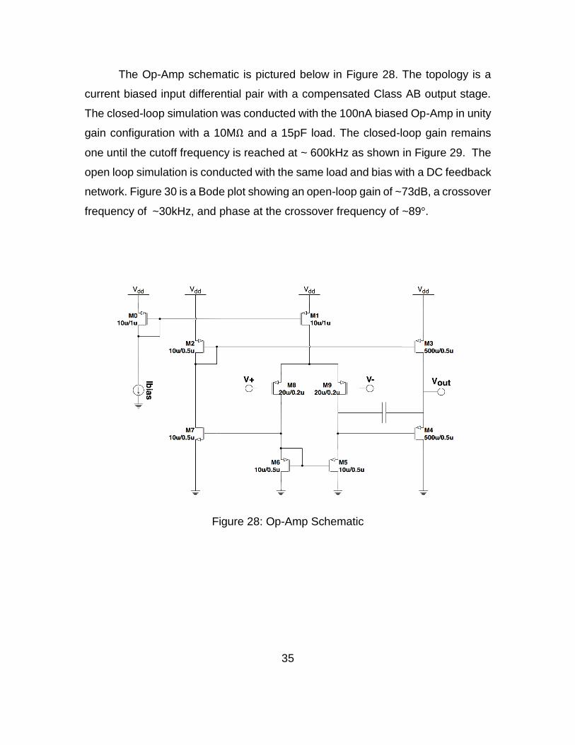
Figure 26: Minch I-V Curve for Bias Currents of 1nA, 10nA, 100nA, and 1uA
Figure 27: Minch Current Gain Sweep
35
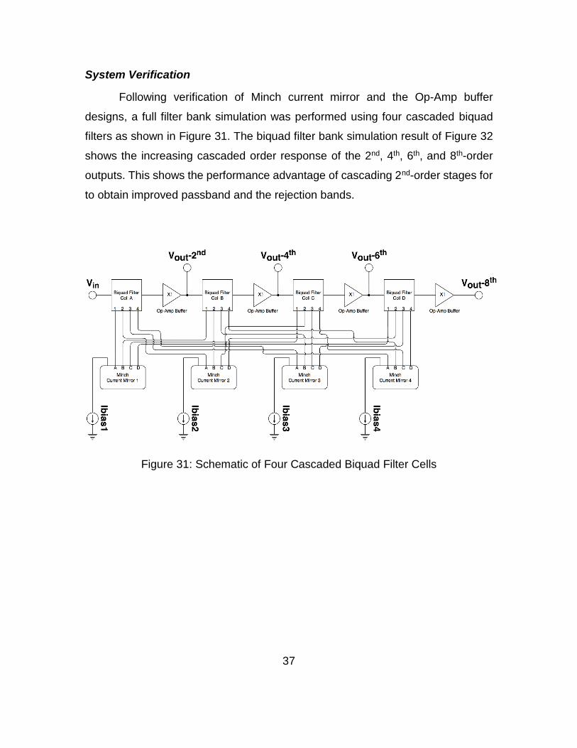
The Op-Amp schematic is pictured below in Figure 28. The topology is a
current biased input differential pair with a compensated Class AB output stage.
The closed-loop simulation was conducted with the 100nA biased Op-Amp in unity
gain configuration with a 10MΩ and a 15pF load. The closed-loop gain remains
one until the cutoff frequency is reached at ~ 600kHz as shown in Figure 29. The
open loop simulation is conducted with the same load and bias with a DC feedback
network. Figure 30 is a Bode plot showing an open-loop gain of ~73dB, a crossover
frequency of ~30kHz, and phase at the crossover frequency of ~89°.
Figure 28: Op-Amp Schematic
36
Figure 29: Op-Amp Closed-Loop Gain
Figure 30: OTA Open-Loop Gain and Phase
37
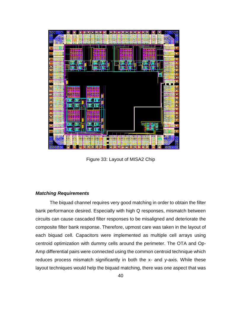
System Verification
Following verification of Minch current mirror and the Op-Amp buffer
designs, a full filter bank simulation was performed using four cascaded biquad
filters as shown in Figure 31. The biquad filter bank simulation result of Figure 32
shows the increasing cascaded order response of the 2nd, 4th, 6th, and 8th-order
outputs. This shows the performance advantage of cascading 2nd-order stages for
to obtain improved passband and the rejection bands.
Figure 31: Schematic of Four Cascaded Biquad Filter Cells
38
Figure 32: Plot of Biquad Filter Bank with 2nd-, 4th-, 6th-, and 8th-Order Responses
Physical Layout Design
Once all the circuit designs were verified using schematic level simulation,
the physical layout of each cell was performed using Cadence Virtuoso Layout
Suite XL. Each layout cell was verified using Mentor Graphics Calibre software and
PDK provided rule decks: Design Rule Check (DRC) and Layout VS Schematic
(LVS). Each hierarchy of designs was placed and routed until the top level was
completed, and then placed and routed into a padframe with ESD protected pads.
Fill materials were then added to the empty space and a seal ring was added to
meet the fabrication foundry requirements. The completed chip layout (MISA2)
was then submitted for fabrication.
39
Floorplan
Each integrated circuit must have a floorplan before tape-out to ensure all
systems and circuits on the chips have been placed and routed correctly and
efficiently. This planning ahead helps realize the full potential of the chip’s area
and pins. For the MISA2 tape-out, it was decided to floorplan the chip for 2 biquad
filter channels, test OTA, test Op-Amp, and an unrelated experimental circuit
design for another student in the bottom right side. The final layout can be viewed
in Figure 33. The top array of biquad filters will be individually programmed for bias
current and can optionally be externally cascaded. The biquad filter channel in the
bottom left corner was internally cascaded with intermediate outputs and utilize
programmed bias currents that are shared across the filter channel using the Minch
current mirror.
40
Figure 33: Layout of MISA2 Chip
Matching Requirements
The biquad channel requires very good matching in order to obtain the filter
bank performance desired. Especially with high Q responses, mismatch between
circuits can cause cascaded filter responses to be misaligned and deteriorate the
composite filter bank response. Therefore, upmost care was taken in the layout of
each biquad cell. Capacitors were implemented as multiple cell arrays using
centroid optimization with dummy cells around the perimeter. The OTA and Op-
Amp differential pairs were connected using the common centroid technique which
reduces process mismatch significantly in both the x- and y-axis. While these
layout techniques would help the biquad matching, there was one aspect that was
41
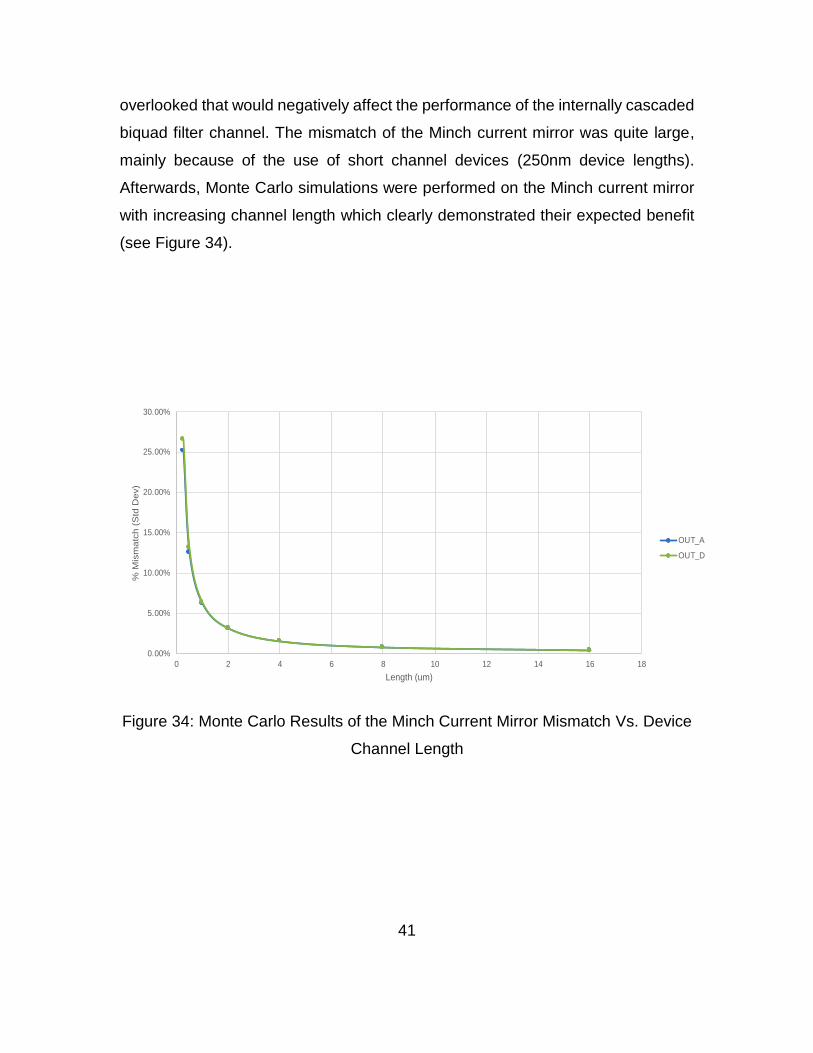
overlooked that would negatively affect the performance of the internally cascaded
biquad filter channel. The mismatch of the Minch current mirror was quite large,
mainly because of the use of short channel devices (250nm device lengths).
Afterwards, Monte Carlo simulations were performed on the Minch current mirror
with increasing channel length which clearly demonstrated their expected benefit
(see Figure 34).
Figure 34: Monte Carlo Results of the Minch Current Mirror Mismatch Vs. Device
Channel Length
0.00%
5.00%
10.00%
15.00%
20.00%
25.00%
30.00%
0 2 4 6 8 10 12 14 16 18
% M
ism
atc
h (
Std
De
v)
Length (um)
Comparison for L = 0.25um, 0.5um, 1um, 2um, 4um, 8um & 16um
OUT_A
OUT_D
42
CHAPTER FOUR
TEST RESULTS
Evaluation
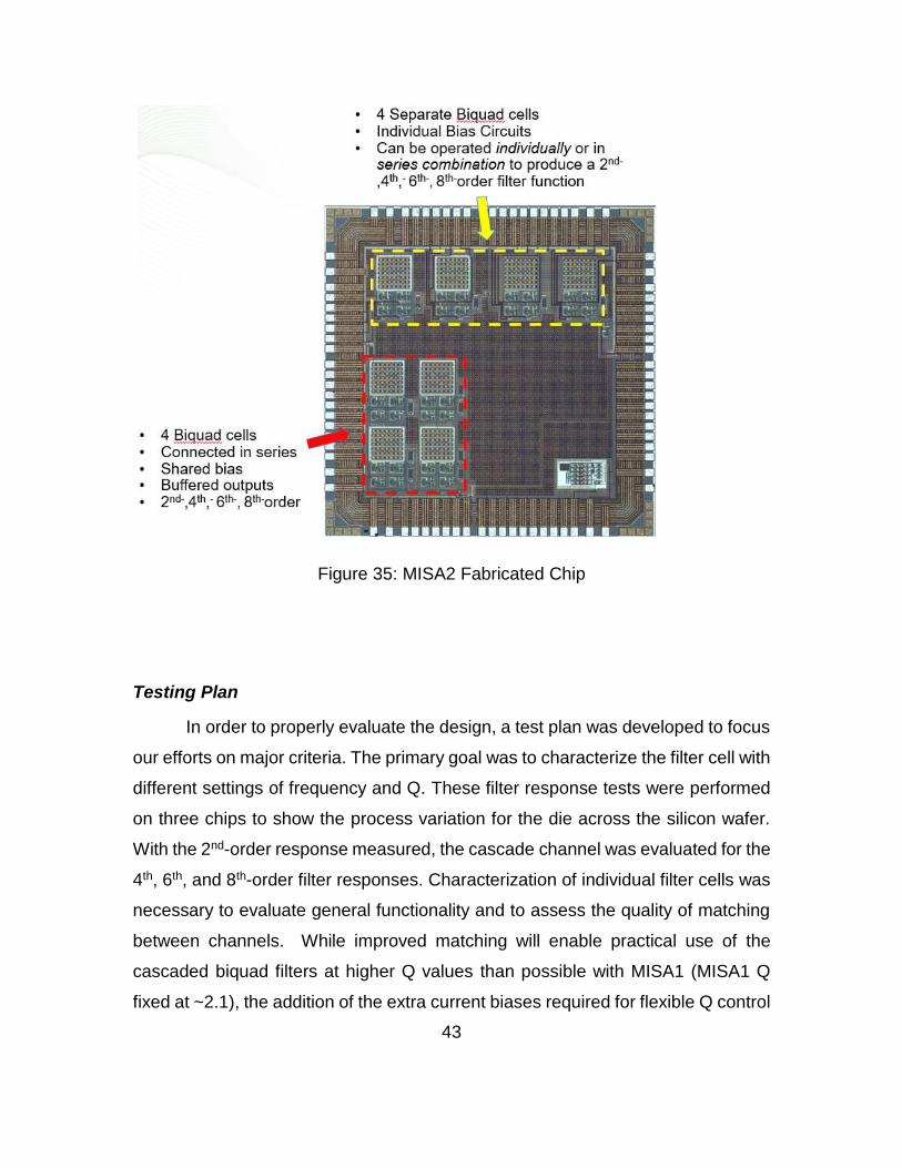
The MISA2 chip design was fabricated in a 180-nm, 1.8-V CMOS process
available through MOSIS. A microphotograph of the chip die, shown in Figure 35,
provides an overview of the two groups of four biquad filter cells. One group
(bottom left) was connected on-chip and shared a single set of bias currents,
replicated by a local Minch current mirror cell. A second grouping of four biquad
filters was also included on the chip (top grouping) with individual connectivity and
bias currents that could be connected for off-chip cascading. Together, these two
configurations allowed evaluation of the individual cells and externally connected
cascaded cells up to 8th order (with individual biasing), as well as evaluation of 2nd
to 8th order on-chip cascaded cells with shared biasing. These circuits enabled
evaluation of the primary enhancements of Biquad filter over the MISA1 design,
namely independent control of the Q and voltage gain. Other parameters of interest
also include the programmed frequency range, power consumption, and matching.
Other criteria evaluated include filter response shape, precision of digital
programming, maximum obtainable quality factor and frequency settings, and
noise levels.
43
Figure 35: MISA2 Fabricated Chip
Testing Plan
In order to properly evaluate the design, a test plan was developed to focus
our efforts on major criteria. The primary goal was to characterize the filter cell with
different settings of frequency and Q. These filter response tests were performed
on three chips to show the process variation for the die across the silicon wafer.
With the 2nd-order response measured, the cascade channel was evaluated for the
4th, 6th, and 8th-order filter responses. Characterization of individual filter cells was
necessary to evaluate general functionality and to assess the quality of matching
between channels. While improved matching will enable practical use of the
cascaded biquad filters at higher Q values than possible with MISA1 (MISA1 Q
fixed at ~2.1), the addition of the extra current biases required for flexible Q control
44
made MISA2 significantly more complicated to program than its MISA1
predecessor. With the 2nd-order response measured, the cascade channel was
measured for a 4th, 6th, and 8th-order filter responses. Figure 35 is a
microphotograph of the fabricated chip and details the differences between the
individual biquads at top and cascaded channel in the top left. Current bias
differences were recorded for the separate filter channels. The programmed bias
settings were given a quantifiable mismatch measurement between filter cells.
These channels will be operated differently and individual biquad channels can be
programmed to mitigate the effects of mismatch while the cascaded channel does
not have this option. The power consumption was measured at the expected
lowest and highest settings for an estimated nominal operation. Auxiliary
measurements conducted determine the linear dynamic range and Total Harmonic
Distortion (THD).
Printed Circuit Board
A test board was designed and fabricated to facilitate both full
characterization of the MISA2 chip and use of the chip in a demonstration system.
The PCB, pictured in Figure 36, facilitated testbed measurements for any individual
biquad filter cell and has headers that can be shorted to form two cascaded 8th-
order channels, or a single 16th-order system. Each main filter input or output is
buffered on board with band-limited Sallen-Key circuits. Additional testing outputs
will also utilize a simple Op-Amp buffer. Modification of the data acquisition
software used for the MISA1 test system was performed to accommodate the eight
current DACs required for the MISA2 filter chip biasing. Each DAC was
programmed to output a voltage across a biasing resistor to generate the desired
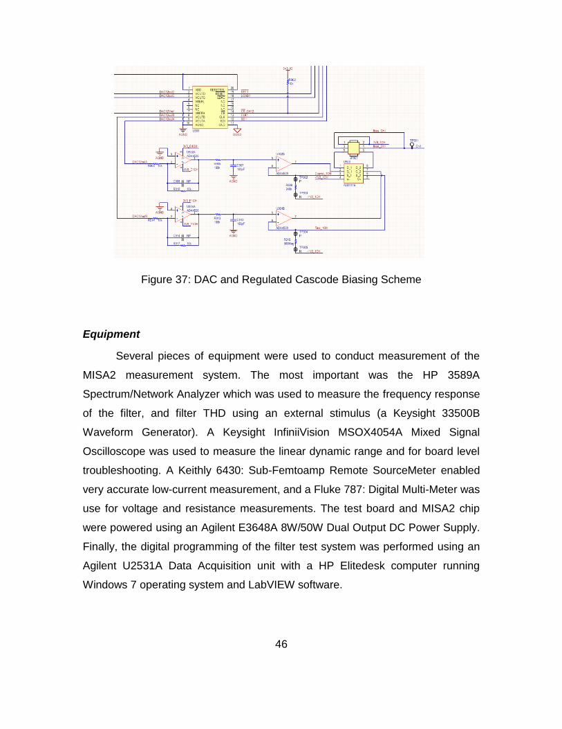
current using the regulated cascode stage (see Figure 37).
45
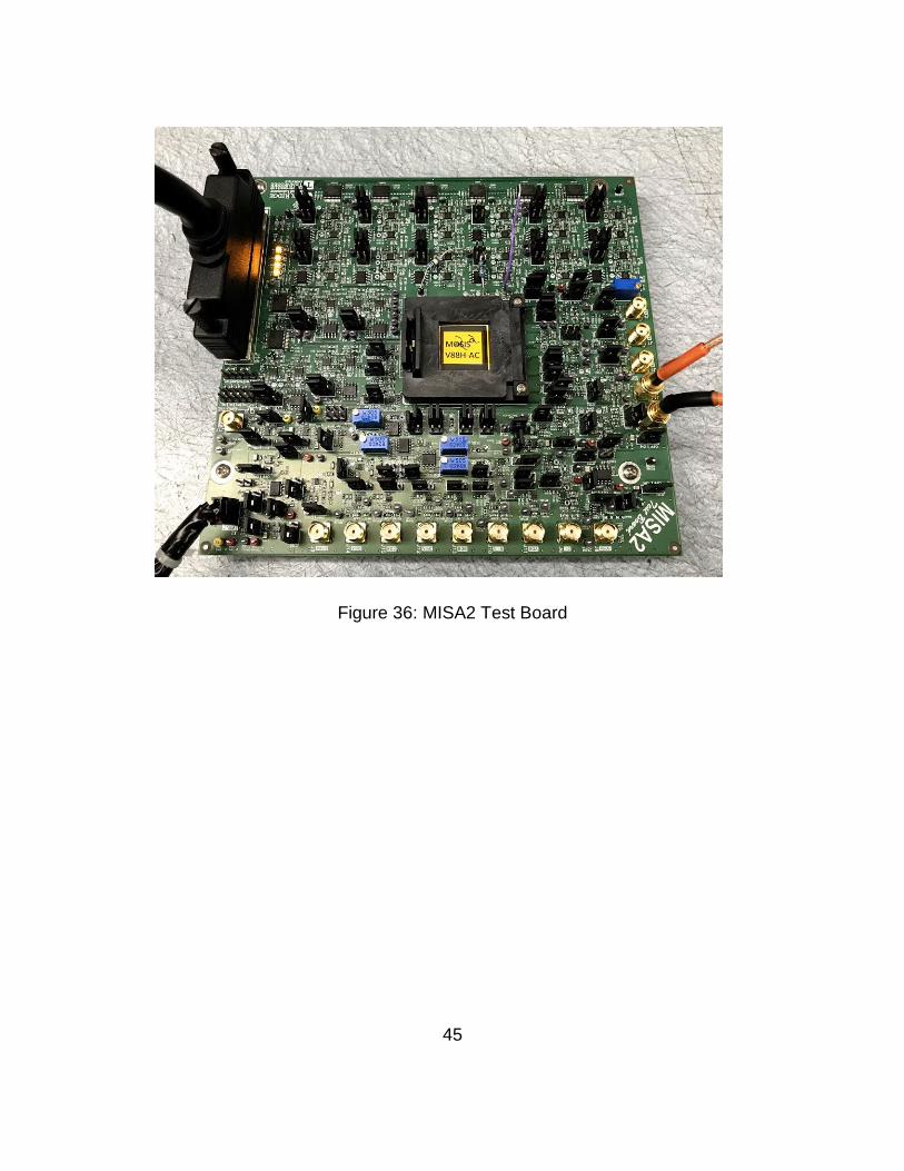
Figure 36: MISA2 Test Board
46
Figure 37: DAC and Regulated Cascode Biasing Scheme
Equipment
Several pieces of equipment were used to conduct measurement of the
MISA2 measurement system. The most important was the HP 3589A
Spectrum/Network Analyzer which was used to measure the frequency response
of the filter, and filter THD using an external stimulus (a Keysight 33500B
Waveform Generator). A Keysight InfiniiVision MSOX4054A Mixed Signal
Oscilloscope was used to measure the linear dynamic range and for board level
troubleshooting. A Keithly 6430: Sub-Femtoamp Remote SourceMeter enabled
very accurate low-current measurement, and a Fluke 787: Digital Multi-Meter was
use for voltage and resistance measurements. The test board and MISA2 chip
were powered using an Agilent E3648A 8W/50W Dual Output DC Power Supply.
Finally, the digital programming of the filter test system was performed using an
Agilent U2531A Data Acquisition unit with a HP Elitedesk computer running
Windows 7 operating system and LabVIEW software.
47
Measurements
Filter Response
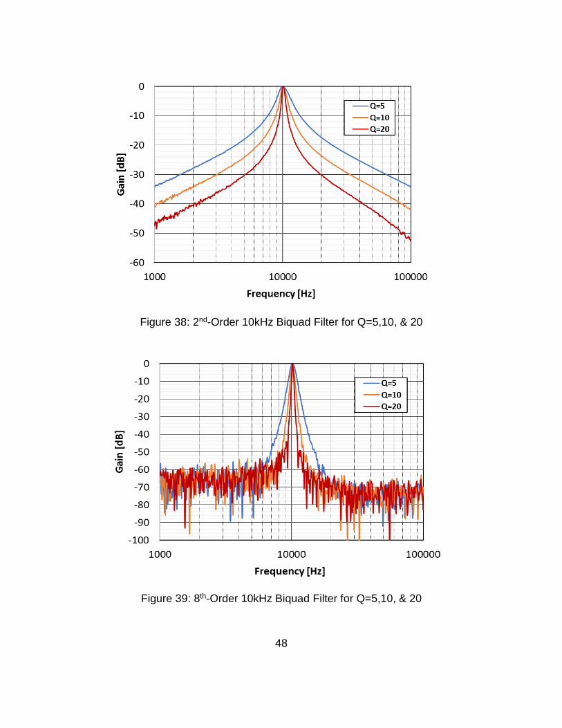
The first measurement conducted was the filter response of a 2nd-order
biquad filter cell programmed at 10kHz, which is the middle of the frequency range.
Figure 38 shows this filter response at low (5), normal (10), and high (20) quality
factor settings. The individual biquad channel was programmed such that each
individual filter cell center frequency aligned precisely producing an 8th-order,
cascaded filter response pictured in Figure 39, shown with increasing spectral
selectivity (Q=5, 10 and 20). These measurements verified the successful
operation of the high Q biquad filter cell and the cascaded filter bank system. The
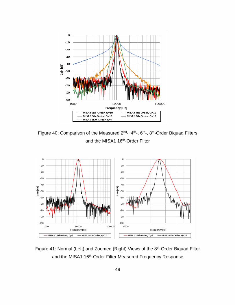
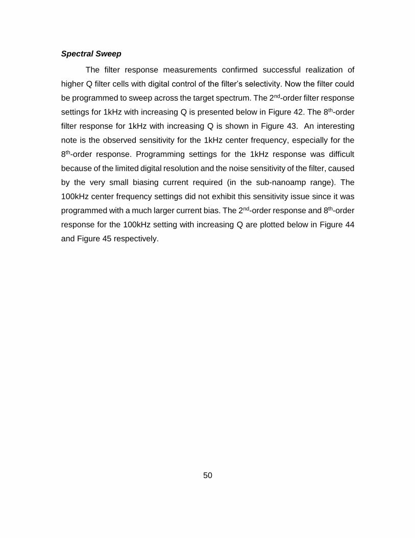
true test was the comparison of the MISA1 16th-order filter channel. In Figure 40,
the MISA2 intermediate outputs (2nd, 4th, 6th, and 8th order responses) were
programmed for a center frequency of 10kHz and Q=10, and are plotted with the
MISA1 16th-order filter for comparison. The 2nd-order biquad surpasses the
effective quality factor of MISA1, but the response sidebands are limited to -40dB
after a decade of frequency, whereas MISA2 response falls to the noise floor after
only an octave of frequency. However, the 6th-order biquad filter response
surpasses the MISA2 filter significantly in both cases. Figure 41 also presents a
comparison of the MISA2 8th-order and MISA1 16th-order and is accompanied with
a two-octave zoomed version. These tests verify the significant improvement in
frequency selectivity obtained by MISA2 over MISA1, at much reduced filter order.
48
Figure 38: 2nd-Order 10kHz Biquad Filter for Q=5,10, & 20
Figure 39: 8th-Order 10kHz Biquad Filter for Q=5,10, & 20
49
Figure 40: Comparison of the Measured 2nd-, 4th-, 6th-, 8th-Order Biquad Filters
and the MISA1 16th-Order Filter
Figure 41: Normal (Left) and Zoomed (Right) Views of the 8th-Order Biquad Filter
and the MISA1 16th-Order Filter Measured Frequency Response
50
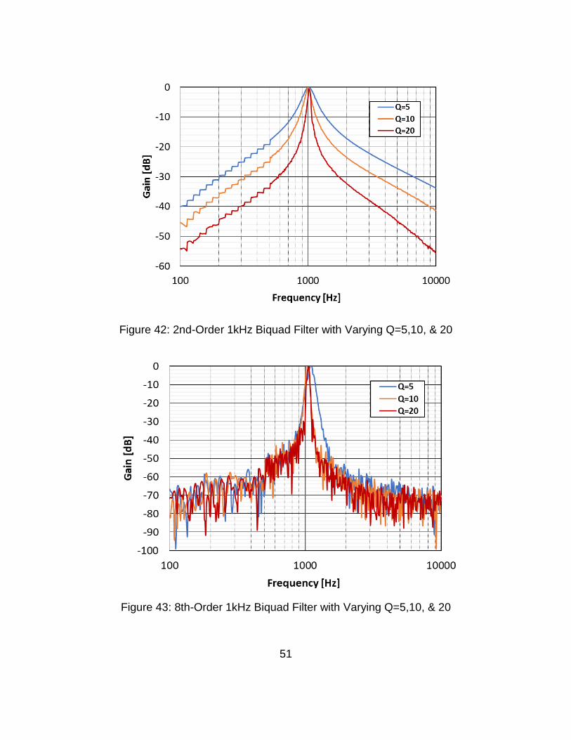
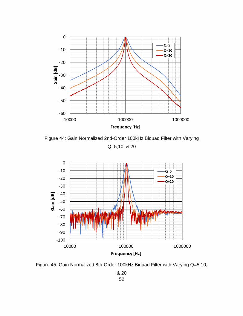
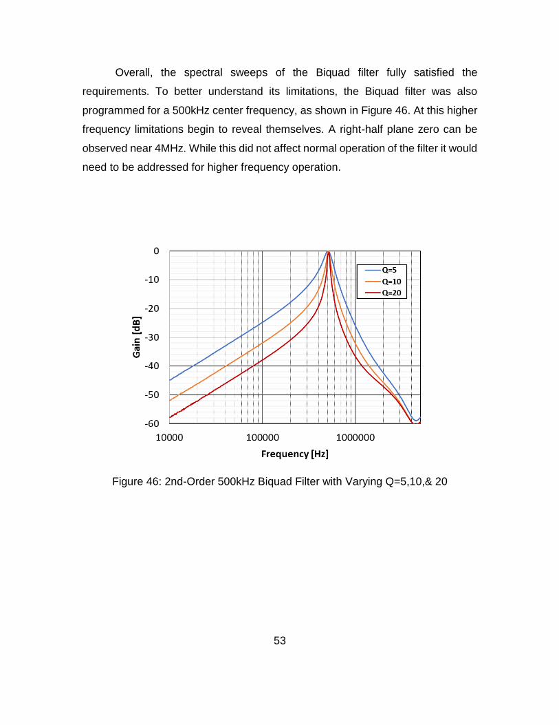
Spectral Sweep
The filter response measurements confirmed successful realization of
higher Q filter cells with digital control of the filter’s selectivity. Now the filter could
be programmed to sweep across the target spectrum. The 2nd-order filter response
settings for 1kHz with increasing Q is presented below in Figure 42. The 8th-order
filter response for 1kHz with increasing Q is shown in Figure 43. An interesting
note is the observed sensitivity for the 1kHz center frequency, especially for the
8th-order response. Programming settings for the 1kHz response was difficult
because of the limited digital resolution and the noise sensitivity of the filter, caused
by the very small biasing current required (in the sub-nanoamp range). The
100kHz center frequency settings did not exhibit this sensitivity issue since it was
programmed with a much larger current bias. The 2nd-order response and 8th-order
response for the 100kHz setting with increasing Q are plotted below in Figure 44