Radu Malureanu,1,3,∗ Maksim Zalkovskij,1,3 Zhengyong Song,2,3
Claudia Gritti,1 Andrei Andryieuski,1 Qiong He,2 Lei Zhou,2 PeterUhd Jepsen,1 and Andrei V. Lavrinenko1
1 Department of Photonics Engineering, Technical University of Denmark, Kgs. Lyngby 2800,Denmark
2 State Key Laboratory of Surface Physics, Key Laboratory of Micro and Nano PhotonicStructures (Ministry of Education), Fudan University, Shanghai 200433, China
Abstract: In this article, we propose a simple scheme to make a metallicfilm on a semi-infinite substrate optically transparent, thus obtaining acompletely transparent electrode in a desired frequency range. By placinga composite layer consisting of dielectric and metallic stripes on top ofthe metallic one, we found that the back-scattering from the metallic filmcan be almost perfectly canceled by the composite layer under certainconditions, leading to transparency of the whole structure. We performedproof-of-concept experiments in the terahertz domain to verify our theoreti-cal predictions, using carefully designed metamaterials to mimic plasmonicmetals in optical regime. Experiments are in excellent agreement withfull-wave simulations.
References and links1. D. S. Hecht, L. Hu, and G. Irvin, “Emerging transparent electrodes based on thin films of carbon nanotubes,
graphene, and metallic nanostructures,” Adv. Mater. 23, 1482–1513 (2011).2. M. Vosgueritchian, D. J. Lipomi, and Z. Bao, “Highly conductive and transparent PEDOT:PSS films with a
fluorosurfactant for stretchable and flexible transparent electrodes,” Adv. Func. Mater. 22, 421–428 (2012).3. R. B. H. Tahar, T. Ban, Y. Ohya, and Y. Takahashi, “Tin doped indium oxide thin films: electrical properties,” J.
App. Phys. 83, 2631–2645 (1998).4. D. R. Cairns, R. P. Witte, D. K. Sparacin, S. M. Sachsman, D. C. Paine, G. P. Crawford, and R. R. Newton,
“Strain-dependent electrical resistance of tin-doped indium oxide on polymer substrates,” App. Phys. Lett. 76,1425–1427 (2000).
5. T. W. Ebbesen, H. J. Lezec, H. F. Ghaemi, T. Thio, and P. A. Wolff, “Extraordinary optical transmission throughsub-wavelength hole arrays,” Nature 391, 667–669 (1998).
6. J. A. Porto, F. J. Garcia-Vidal, and J. B. Pendry, “Transmission resonances on metallic gratings with very narrowslits,” Phys. Rev. Lett. 83, 2845–2848 (1999).
7. H.-T. Chen, J. Zhou, J. F. OHara, F. Chen, A. K. Azad, and A. J. Taylor, “Antireflection coating using metamate-rials and identification of its mechanism,” Phys. Rev. Lett. 105, 073901 (2010).
8. L. Zhou, W. Wen, C. T. Chan, and P. Sheng, “Electromagnetic-wave tunneling through negative-permittivitymedia with high magnetic fields,” Phys. Rev. Lett. 94, 243905 (2005).
#172483 - $15.00 USD Received 12 Jul 2012; revised 11 Sep 2012; accepted 12 Sep 2012; published 20 Sep 2012(C) 2012 OSA 24 September 2012 / Vol. 20, No. 20 / OPTICS EXPRESS 22770
10. D. Bergman, “The dielectric constant of a composite material - a problem in classical physics,” Phys. Rep. 43,377–407 (1978).
11. K. Busch, C. T. Chan, and C. M. Soukoulis, in Photonic Band Gap Materials edited by C. M. Soukoulis (Kluwer,Dordrecht, 1996) 16, 267–269 (1999).
12. J. B. Pendry, A. J. Holden, W. J. Stewart, and I. Youngs, “Extremely low frequency plasmons in metallicmesostructures,” Phys. Rev. Lett. 76, 4773–4776 (1996).
13. M. Naftaly, and R. E. Miles, “Terahertz time-domain spectroscopy of silicate glasses and the relationship tomaterial properties,” J. Appl. Phys. 102, 043517 (2007).
properties of the metals Al, Co, Cu, Au, Fe, Pb, Ni, Pd, Pt, Ag, Ti, and W in the infrared and far infrared,” Appl.Opt., 22,1099–1119 (1983).
16. N. J. Cronin, ‘in Microwave and Optical Waveguides (Taylor & Francis, 1995).17. C. A. Balanis, in Advanced Electromagnetics Engineering (Prentice Hall, 1989).18. P. Yeh, in Optical Waves in Layered Media (Wiley Online library, 1988).
1. Introduction
For developing the new generation of electronic devices, varying from solar cells to electronicpaper, touch screens, and displays, there is a clear need for transparent contact electrodes(TCEs) [1]. We define such contacts by their possibility of allowing a certain portion of theelectromagnetic spectra of interest to pass through the contacts while, in the same time, main-taining the electrical connections intact. The research in this field is developed mainly towardstransparent conductive oxides, conjugated polymers, colloidal semiconductors, and carbon al-lotropes in order to obtain low-cost and large-scale compatible electrodes [2]. Nowadays, themost promising material for TCEs is Indium-Tin-Oxide (ITO) [3]. Although it shows clear ad-vantages with respect to its competitors, ITO comes with the inherent limitations. On one side,the scarcity and continuous increase in the price of indium, the main component of ITO is ofgreat concern for an eventual implementation in the everyday devices. On the other, ITO is verybrittle thus making devices like electronic paper or flexible screens difficult to achieve [4]. Adifferent approach consists in using noble metals (such as Au, Ag etc.) to make TCEs. How-ever, such materials are intrinsically opaque for light due to their high plasma frequency, andtherefore, one has to structure these metals in various shapes to make them transparent withina certain frequency window [5, 6]. However, structuring may decrease the mechanical stabilityand electric conductivity of a metallic contact layer, what is undesired in practical applications.In addition, most previous efforts have been devoted to making free-standing TCEs, but in manyreal applications such as solar cells, the TCEs should function being deposited on a substrate,generally silicon (Si). In this case, the substrate itself having a high refractive index may inducesubstantial reflections, which should be avoided in applications. Therefore, it is highly desiredto consider more realistic geometry when designing TCEs.
In [7], the authors suggest a new approach for fabricating anti-reflective coatings using Fabry-Perot resonances, where the cavity length is much smaller than the wavelength. Although ourresults in suppressing reflections are similar we are standing on other theoretical platform -scattering cancellation. The scattering cancellation method that we apply, can be, in principle,exploited to find the path to broadband functioning through the careful design of the top layer.We provide also an alternative route in designing of such structures based on the transmissionline approach. It shows connection to both scattering cancellation and the Fabry-Perot models.Moreover, it allows to identify the most critical parameters influencing the bandwidth and thetransparency window position.
In this work, we propose a simple scheme that can make a continuous and unstructuredplasmonic metal film on top of a semi-infinite substrate, optically transparent in certain fre-quency windows. We first introduce the scheme and discuss the underlying physics in Sec. 2.
#172483 - $15.00 USD Received 12 Jul 2012; revised 11 Sep 2012; accepted 12 Sep 2012; published 20 Sep 2012(C) 2012 OSA 24 September 2012 / Vol. 20, No. 20 / OPTICS EXPRESS 22771
Specifically, as a proof of concept, we then choose the terahertz (THz) domain to verify ourtheoretical predictions (Section 3). An alternative transmission line model is introduced in Sec.4. The model was validated in straight characterization. We describe the THz sample fabrica-tion procedures in Sec. 5, and present our experimental results in Sec. 6, comparing them withthe full wave simulation results. We conclude our paper in the last section.
2. Transparency by scattering cancellation - designing principle
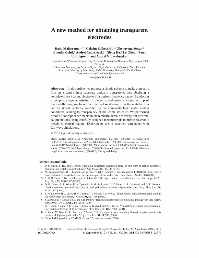
Our scheme is inspired by early work [8] showing that an optically opaque layer (with a negativepermittivity ε) can be perfectly transparent when sandwiched between two carefully designedmetamaterial (MTM) layers. The physics behind obtaining the transparency is the cancellationof the scattering from the target opaque layer by carefully choosing the material and geomet-rical parameters of those two MTM layers. In the present problem, considering a continuousmetal film C (with negative relative permittivity εC) on top of a semi-infinite substrate withrelative permittivity εsub, our aim is to transmit in the most effective way electromagnetic (EM)waves through the C layer inwards the semi-infinite substrate. To achieve this goal we purposelyplaced a composite layer consisting of alternate A and B stripes (denoted as AB layer) on topof the C layer, as shown in Fig. 1(a). The width of the strips A and B are respectively denotedby wA and wB, and the periodicity of layer AB is P = wA +wB. Meanwhile, the thicknesses oflayers AB and C are respectively dAB and dC.
To illustrate how the idea works, we performed full-wave numerical simulations based onthe finite-element-method [9] to investigate the EM wave transmittance as functions of εB andP/λ . The results are depicted in Fig. 1(b) with all other parameters fixed at the following values:εA = εsub = 12, εC =−40, wB = 0.1λ0, dAB = dC = 0.02λ0, where λ0 is the wavelength of inci-dent light in free space. In our calculations we fixed wB and vary wA to change P. According tothe phase diagram depicted in Fig. 1(b), we find that the entire system becomes perfectly trans-parent when the geometrical and material parameters satisfy certain conditions. This is quitesurprising at first glance, since the transmittance of a standing-alone C layer on the substrateis only ∼ 20%. However, with an additional AB layer put on its top, we can identify two mainEM bands with transmittance values close to 100%.
Ek
Fig. 1. (a) Schematic illustration of the proposed structure. (b) Transmittance (colorfulscale) as the function of εB and P/λ . All other parameters are fixed, as described in thetext.
We find that the discovered transparency phenomenon can be explained by the scatteringcancellation mechanism in the same spirit as in [8]. Since the transparency region is whereP << λ0, we homogenize the composite AB layer based on the effective medium theory [10].Such approximation greatly simplifies our considerations but helps capture the main physics.In the long wavelength limit, for the particular polarization E||y, the effective permittivity ofthe AB layer can be obtained by:
#172483 - $15.00 USD Received 12 Jul 2012; revised 11 Sep 2012; accepted 12 Sep 2012; published 20 Sep 2012(C) 2012 OSA 24 September 2012 / Vol. 20, No. 20 / OPTICS EXPRESS 22772
1εAB
=1εA
· wA
P+
1εB
wB
P. (1)
We can then employ the standard transfer-matrix-method (TMM) [11] to analytically cal-culate the transmittance/reflectance coefficients through the whole layered structure, e.g.air/AB/C/substrate.
(t0
)= Q ·
(1r
). (2)
where t = Q11 −Q12Q21/Q22 and r = −Q21/Q22 are respectively the transmittance and re-flectance coefficients, and Q is the 2× 2 scattering matrix of the system. In the ideal losslesscase perfect transparency corresponds to zero reflectance, i.e., Q21 = 0. Therefore, analysis offunction Q21 will give us some directions for achieving transparency. Through straightforwardbut tedious calculations, we found that:
Q21 =(
1− 1√εsub
)+ i ·
[(1√|εC|
+
√|εC |√εsub
)tanh
(√|εC|dC/λ0
)]+
+i ·[(
1√εAB−
√εAB√εsub
)tan(
√εABdAB/λ0)
]− (3)
−( √εAB√
|εC|+
√|εC|√εAB√εsub
)tan(
√εABdAB/λ0) tanh
(√|εC|dC/λ0
)
We note that all terms in Eq. (3) have clear physical interpretations. The first two terms rep-resent scattering from the semi-infinite substrate and the C layer, respectively. The third term isclearly contributed by the AB layer. Finally the forth term results from multiple scattering in alllayers. It is obvious from Eq. (3) that the presence of the AB layer can generate additional scat-tering terms (the last two ones) to cancel those contributed by the C layer and the semi-infinitesubstrate. However, different from [8], we find that function Q21 is complex having both realand imaginary parts. Therefore, satisfying condition Q21 = 0 by tuning only one parameter εAB
is not guaranteed. To understand the phase diagram presented in Fig. 1(b), we relax the perfecttransparency condition. Instead of solving equation Q21 = 0 accurately, we vary parameter wA,while keeping all other parameters fixed, to find the solutions that minimize quantity |Q21/Q22|.In this analysis we can omit Q22 since it is a smooth function of wA with very large values, sothe important parameter determining the reflectance is apparently Q21. The solutions obtainedby the minimization procedure are depicted in Fig. 1(b) with the open circles. We find the FEMsimulated transparency bands match quite well with the minimization model results, indicat-ing that the present discovered transparency is indeed governed by the scattering cancellationmechanism. Specifically, adjusting parameter wA can efficiently modulate the scattering fromthe AB layer so that the reflectance from the system is minimized (see (Eq.) 3)), leading to thesignificantly enhanced EM wave transmittance.
The discrepancies between the full-wave simulations and model results are found mainly forthe upper branch and in the right part of the graph. It is easily understandable since in theseregions the structure cannot be considered deeply sub-wavelength, so that the effective mediumdescription of the AB layer is not correct anymore. It is interesting to note that, while theeffective medium model considerations do not guarantee the existence of perfect transparency,the full-wave simulations on realistic structures show that the maximized transmittance in eachcase can indeed be almost 100%.
#172483 - $15.00 USD Received 12 Jul 2012; revised 11 Sep 2012; accepted 12 Sep 2012; published 20 Sep 2012(C) 2012 OSA 24 September 2012 / Vol. 20, No. 20 / OPTICS EXPRESS 22773
3. Transparent THz electrode
Although the illustrative example presented above is very particular, our approach can be ex-panded to any parameter set due to the generality of the involved formulae. Once the C layerproperties are known, the AB-layer parameters can be deduced. Also, the concept is applicableto any EM frequency domain as long as the required material parameters can be realized. Themost natural applications of our design are in the visible domain, where the permittivities ofplasmonic metals are in the desired region (see Fig. 1). Nevertheless, to verify the concept ex-perimentally we decided to apply it in the THz domain to avoid notorious fabrication challengesof nanophotonics.
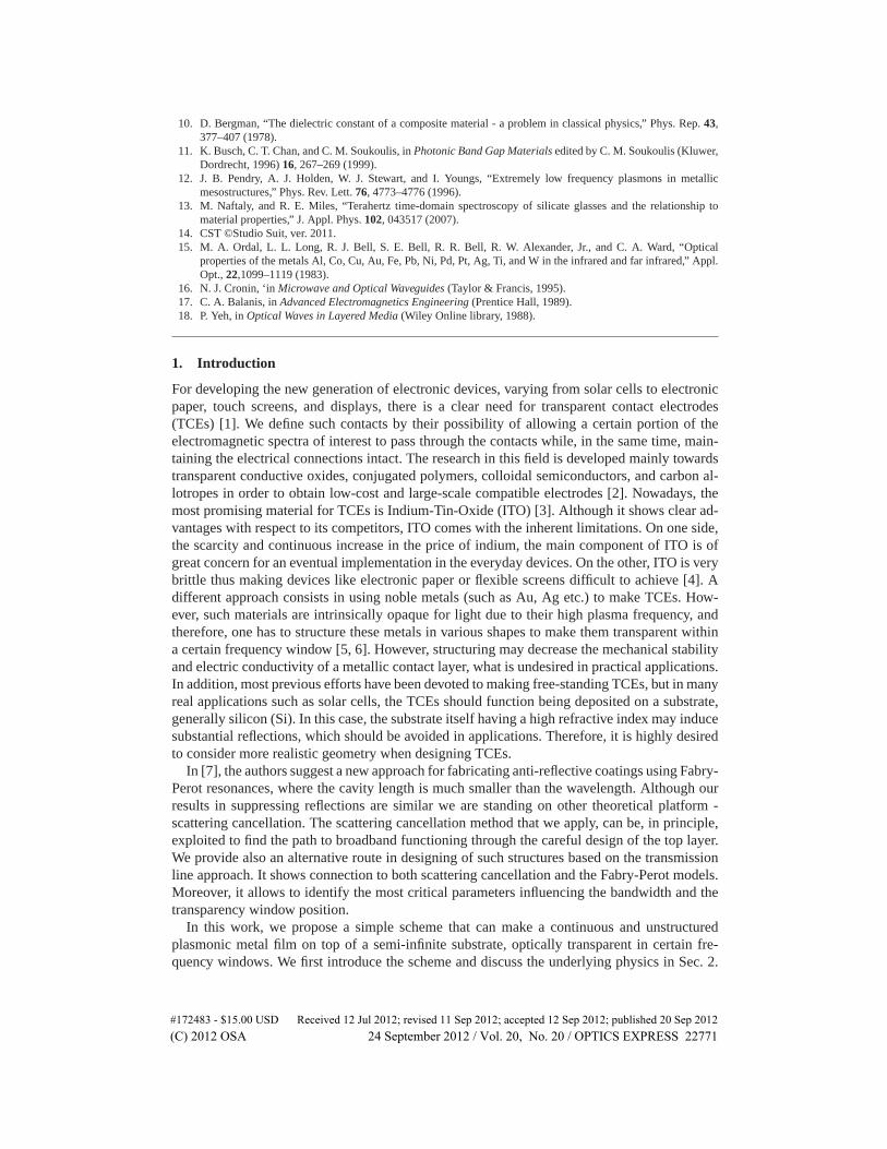
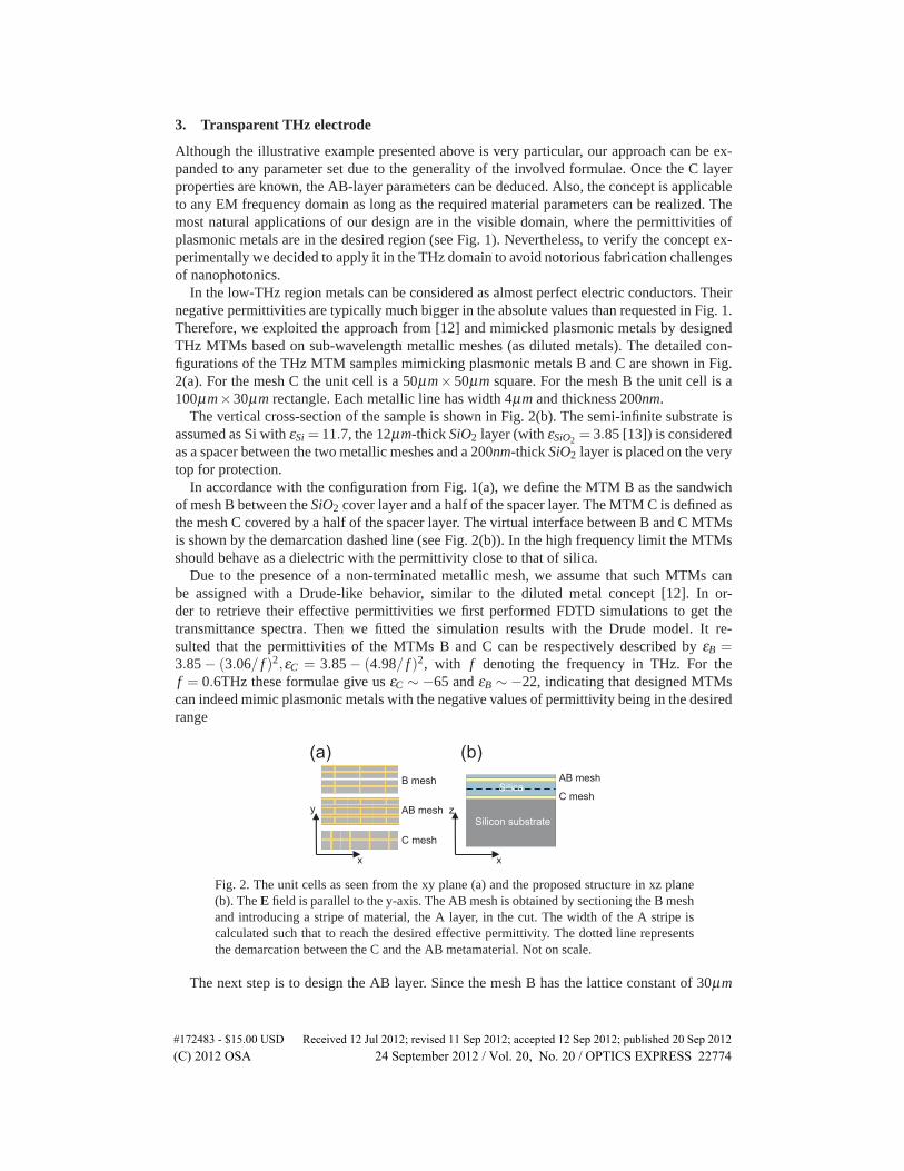
In the low-THz region metals can be considered as almost perfect electric conductors. Theirnegative permittivities are typically much bigger in the absolute values than requested in Fig. 1.Therefore, we exploited the approach from [12] and mimicked plasmonic metals by designedTHz MTMs based on sub-wavelength metallic meshes (as diluted metals). The detailed con-figurations of the THz MTM samples mimicking plasmonic metals B and C are shown in Fig.2(a). For the mesh C the unit cell is a 50μm× 50μm square. For the mesh B the unit cell is a100μm×30μm rectangle. Each metallic line has width 4μm and thickness 200nm.
The vertical cross-section of the sample is shown in Fig. 2(b). The semi-infinite substrate isassumed as Si with εSi = 11.7, the 12μm-thick SiO2 layer (with εSiO2 = 3.85 [13]) is consideredas a spacer between the two metallic meshes and a 200nm-thick SiO2 layer is placed on the verytop for protection.
In accordance with the configuration from Fig. 1(a), we define the MTM B as the sandwichof mesh B between the SiO2 cover layer and a half of the spacer layer. The MTM C is defined asthe mesh C covered by a half of the spacer layer. The virtual interface between B and C MTMsis shown by the demarcation dashed line (see Fig. 2(b)). In the high frequency limit the MTMsshould behave as a dielectric with the permittivity close to that of silica.
Due to the presence of a non-terminated metallic mesh, we assume that such MTMs canbe assigned with a Drude-like behavior, similar to the diluted metal concept [12]. In or-der to retrieve their effective permittivities we first performed FDTD simulations to get thetransmittance spectra. Then we fitted the simulation results with the Drude model. It re-sulted that the permittivities of the MTMs B and C can be respectively described by εB =3.85 − (3.06/ f )2,εC = 3.85 − (4.98/ f )2, with f denoting the frequency in THz. For thef = 0.6THz these formulae give us εC ∼ −65 and εB ∼ −22, indicating that designed MTMscan indeed mimic plasmonic metals with the negative values of permittivity being in the desiredrange
z
x
y
x
(a) (b)
AB mesh
C mesh
Silicon substrate
Silica
AB mesh
C mesh
B mesh
Fig. 2. The unit cells as seen from the xy plane (a) and the proposed structure in xz plane(b). The E field is parallel to the y-axis. The AB mesh is obtained by sectioning the B meshand introducing a stripe of material, the A layer, in the cut. The width of the A stripe iscalculated such that to reach the desired effective permittivity. The dotted line representsthe demarcation between the C and the AB metamaterial. Not on scale.
The next step is to design the AB layer. Since the mesh B has the lattice constant of 30μm
#172483 - $15.00 USD Received 12 Jul 2012; revised 11 Sep 2012; accepted 12 Sep 2012; published 20 Sep 2012(C) 2012 OSA 24 September 2012 / Vol. 20, No. 20 / OPTICS EXPRESS 22774
along the y-axis, we must take the width wB of stripe B as n× 30μm with n and integer whendesigning the AB layer. Otherwise the stripes B may not have the same properties as the originalB mesh. Taking material A as silica, we set the widths of stripes A and B as wA = 10μm andwB = 30μm (see Fig. 2(a)). The AB layer thus obtained is placed on top of the C layer andwe obtain the final design shown in Fig. 2(b). Through comparing the transmission spectracalculated with a homogenous effective-medium slab and full-wave simulations on the realisticAB structure, we found that the effective permittivity of the AB layer can be given by εAB =3.85+4.19/(0.742− f 2). The resonance behavior of εAB ensures that there must be a frequencywhere it exhibits the desired value to make the whole structure transparent.
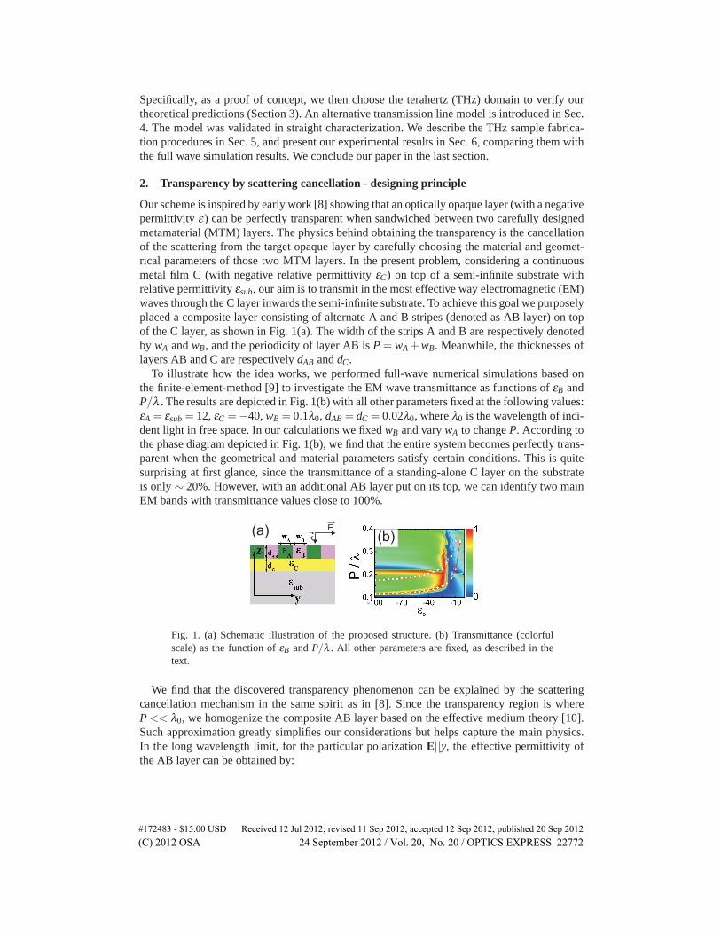
We performed FDTD simulations [14] based on realistic material parameters to study thetransmittance spectrum T = |S21|2 through the designed structure. In our calculations all ma-terials are assumed to be non-magnetic (μ = μ0), and the dielectric function of aluminum isdescribed using the Drude model with parameters from [15]. In the case of a bare Si substrateof 530μm thickness the calculated transmittance is ∼ 70%. As expected, the C layer greatlydiminishes the transmittance down to ∼ 30%. However, by putting the AB layer on top of theC layer we can reach almost 100% transmittance at 0.57THz (see Fig. 3(a)). It is worth notingthat the incident wavelength is roughly 40 times larger than the thickness (∼ 12.7μm) of theAB layer. Yet, by appropriately adjusting the material and geometric parameters of such thinAB layer, we can make its scattering strong enough to completely compensate the scatteringfrom the C layer, leading to nearly perfect transparency. The entire device thus combines highoptical transmittance with good in-plane electric conductivity, which is highly desired in manyoptoelectronic applications.
Fig. 3. (a) simulated transmittance (red) and reflectance (blue) spectra of the proposedconfiguration in Fig. 2 (solid line) as well as of the simple C-layer mesh (dash line). (b)the compared transmittance of ideal and randomized structure. (c) and (d) respectivelyrepresent the behavior of the structure when varying the incidence angle in the (x,z) planeand (y,z) plane. The incident field is polarized along the Y axis
We also simulated the imperfection tolerance of the design by introducing deviationsfrom the ideal structure parameters. In Fig. 3(b) the transmittance results are shown for or-dered and randomized structures. The randomness was introduced by varying the wA within10× (1±40%)μm while keeping the other parameters constant. Although there is a slight shiftof about 10GHz in the spectra, it is basically negligible from the practical point of view. Such
#172483 - $15.00 USD Received 12 Jul 2012; revised 11 Sep 2012; accepted 12 Sep 2012; published 20 Sep 2012(C) 2012 OSA 24 September 2012 / Vol. 20, No. 20 / OPTICS EXPRESS 22775
pronounced tolerance for parameters changes is extremely important for implementing the de-vice in real-life applications, where the fabrication imperfections and the in-situ variations canotherwise hinder its functionality.
The proposed transparency is rather insensitive to the incidence angle. The simulated trans-mittance as function of incidence angle and frequency f are shown in Figs. 3(c) and 3(d) for θx
and θy respectively. The transparency is stable within the extended range of incidence anglesθy ∼ 60◦ and θx ∼ 35◦.
4. Transmission line model
Another view on the the transparent electrodes performance can be given using the transmis-sion line analogy that is applicable in the long-wavelength regime. The transmission line (TL)approach is a common language in the microwave engineering. It provides important insight tohow the metamaterial surface should be modified in order to reach the desired functionality, forexample, to modify the resonant frequency, bandwidth or transmittance amplitude.
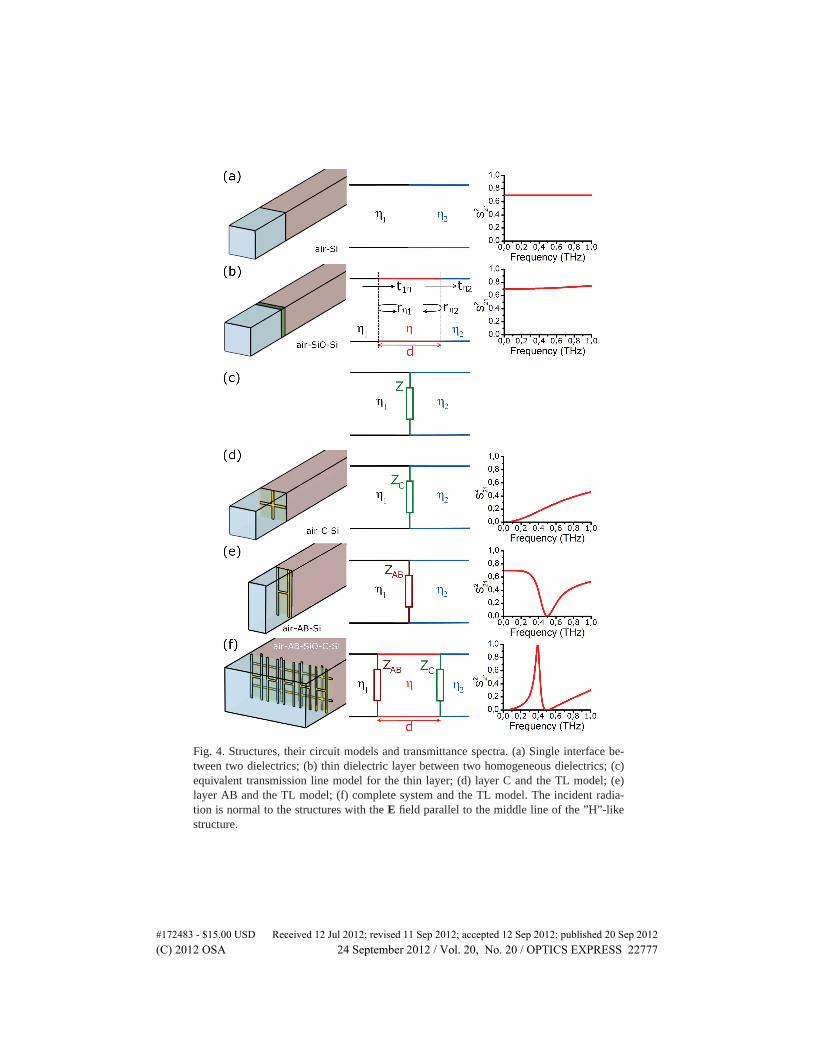
Propagation of a plane wave in a homogeneous dielectric may be considered as propagation(for example, along z-axis) of the fundamental mode in a dielectric filled rectangular waveguide(a× b) with the perfect electric (x-) and perfect magnetic (y-) boundaries [16, 17]. In suchhomogeneous transmission line the x-polarized electric field E is connected with the voltagethrough V = aE and y-polarized magnetic field H is linked with the current through I = bH.The relation between the electric and magnetic fields is described by the wave impedance η =
E/H =√
μμoεε0
, while the relation between the voltage and current is described through the
characteristic impedance ZC = VI = aE
bH = aη/b. The transmittance through a single interface(see Fig. 4(a)) between two dielectrics (η1 and η2) is equal to
T =4η1η2
(η1 +η2)2 (4)
For a bare silicon substrate (η2 = 0.29Z0) in air (η1 = Z0 = 120πΩ) the transmittance isT = 0.7.
A dielectric layer (with impedance η) of thickness d between two other semiinfinite di-electrics (η1 and η2) is analogous to a short transmission line section inserted between twoother transmission lines (see Fig. 4(b)). The transmittance through it can be calculated with theAiry formulas [18]
T =η1
η2
∣∣∣∣ t1η tη2
1− rη1rη2 exp(ikd)
∣∣∣∣2
(5)
The meaning of the amplitude transmittance and reflectance coefficients t1η , tη2,rη1,rη2 isclear from the central panel of Fig. 4(b). The exponential term accounts for the phase advanceupon propagation through the layer.
For our structure we used a very thin dielectric layer d = 12μm comparing to the wavelengthof electromagnetic radiation (λ ∼ 600μm), so the working frequency is far lower than the firstFabry-Perot resonance and the transmittance is almost the same as the one through the silicon-air interface.
Adding an electrically thin (thickness is much smaller than the wavelength) structured metal-lic layer (or metamaterial surface) to the interface between two dielectrics (see Fig. 4(c)) isequivalent to adding shunt impedance Z = aηeq/b, which is an impedance of the unit cell, atthe point where the transmission lines are connected. The amplitude transmittance t and re-flectance r coefficients are then:
#172483 - $15.00 USD Received 12 Jul 2012; revised 11 Sep 2012; accepted 12 Sep 2012; published 20 Sep 2012(C) 2012 OSA 24 September 2012 / Vol. 20, No. 20 / OPTICS EXPRESS 22776
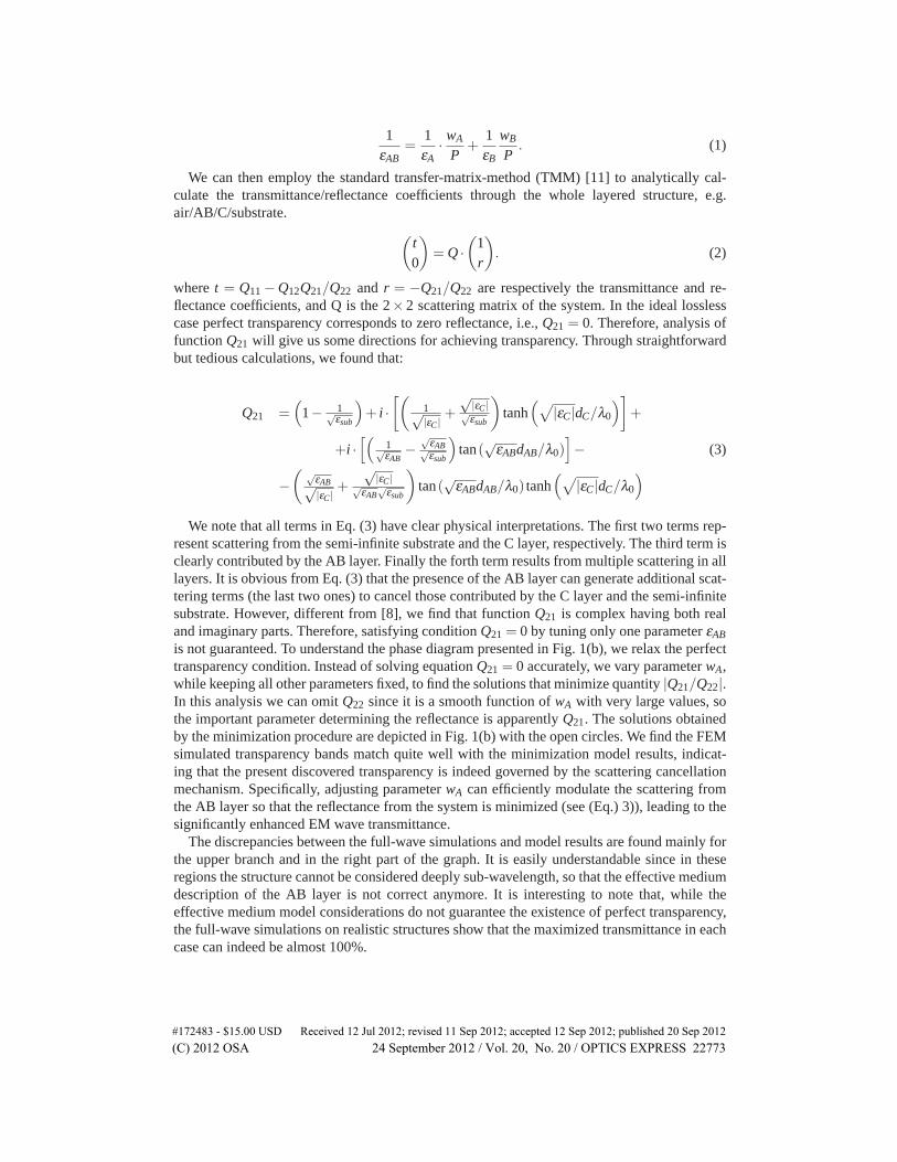
Fig. 4. Structures, their circuit models and transmittance spectra. (a) Single interface be-tween two dielectrics; (b) thin dielectric layer between two homogeneous dielectrics; (c)equivalent transmission line model for the thin layer; (d) layer C and the TL model; (e)layer AB and the TL model; (f) complete system and the TL model. The incident radia-tion is normal to the structures with the E field parallel to the middle line of the ”H”-likestructure.
#172483 - $15.00 USD Received 12 Jul 2012; revised 11 Sep 2012; accepted 12 Sep 2012; published 20 Sep 2012(C) 2012 OSA 24 September 2012 / Vol. 20, No. 20 / OPTICS EXPRESS 22777
t =
2η1
1η1
+ 1η2
+ 1ηeq
(6)
r =
1η1
− 1η2
− 1ηeq
1η1
+ 1η2
+ 1ηeq
, (7)
where the equivalent wave impedance ηeq = bZ/a. A highly conductive layer (Z = 0) makes ashort circuit, so the incoming wave is fully reflected back. A very high impedance (Z >> η)is equivalent to an open circuit and the wave is transmitted through the interface as there is noimpedance (no any thin layer) at all. In the case of a metamaterial surface its impedance can bequalitatively estimated by constructing an equivalent LRC-circuit. The simple modeling is thata wire along the electric field corresponds to an inductance and a resistance, and a dielectricgap gives a capacitance.
Let’s now consider our design parts C, AB and the whole structure ABC - by the TL ap-proach. To calculate the transmittance through two thin metamaterial layers separated with adielectric one, we should use Eq. (5) with the reflectance and transmittance coefficients modi-fied according to Eqs. (6) and (7). For the qualitative explanation we neglect the Ohmic losses.
The mesh C in our design consists of crossing wires (Fig. 4(d)). Assuming that we canneglect the capacity between the wires it’s impedance ZC = −iωLC is purely determined byinductance LC (we use the optical convention for the phase factor exp(−iωt)). Consequently,at low frequencies impedance ZC is low comparing to η1,2, and the layer C acts as a high-frequency filter (see the right panel of Fig.4(d).
The layer AB (Fig. 4(e)) consists of short vertical metal wires (inductance LAB) with a gapbetween horizontal wires (capacitance CAB). Its impedance ZAB = −i(ωLAB − 1
ωCAB) is high
at low frequencies (ω << 1√LABCAB
) and at high frequencies (ω >> 1√LABCAB
), but close to
zero near the resonance (ωAB = 1√LABCAB
). Thus the layer AB itself acts as a rejection filterprohibiting transmission in a narrow band near the resonance - the right panel of Fig. 4(e).
Together the ABC system corresponds to an equivalent transmission line shown in Fig. 4(f) ifwe assume, for simplicity, that the mutual inductance between the two layers can be neglected.We regard the AB and C layers as two impedances (see Fig. 1) connected in parallel and thushaving the total impedance:
Ztotal =Z1Z2
Z1 +Z2=−i
ωLC(ωLAB − 1ωCAB
)
ω(LC +LAB)− 1ωCAB
(8)
Impedance Ztotal is zero (so no transmission) at the AB resonance frequency ωAB = 1√LABCAB
.
In contrary it is very large at frequency ωABC = 1√(LAB+LC)CAB
< ωAB that leads to a very high
transmission close to 100%. We should emphasize that the ABC structure is not only able torecover the transmission from very low to the order of that at the silicon-air interface, but alsoto overcome this level and provide theoretically full transparency.
Another explanation of this peak (the Fabry-Perot picture) can be given if we account fora thin dielectric layer between the metallic AB and C meshes. As we mentioned before, thethickness of the dielectric (silica) between AB and C layers d = 12μm is much smaller thanthe wavelength of the used THz radiation (600μm), so the silica layer itself cannot give a hightransmission satisfying the first Fabry-Perot resonance condition: the total phase advance duringthe back and forth propagation in the resonator should be equal to 2π . However, the phase ofthe electromagnetic wave experiences large changes upon the reflection from the AB and C
#172483 - $15.00 USD Received 12 Jul 2012; revised 11 Sep 2012; accepted 12 Sep 2012; published 20 Sep 2012(C) 2012 OSA 24 September 2012 / Vol. 20, No. 20 / OPTICS EXPRESS 22778
meshes near frequency ωABC, so it becomes possible to satisfy the Fabry-Perot phase conditioneven with a very small dielectric layer. Consequently, we observe a high transmission peak [7].
The TL approach gives not only a simple explanation of the observed effects, but also a goodadvice on the structure modification in order to reach the desired functionality. For example,if one wishes to decrease the frequency of the high transmission peak, one has to increasecapacitance CAB by making, for example, the gap between the horizontal wires smaller.
SiliconAluminumPhotoresistSilica
1 3 42
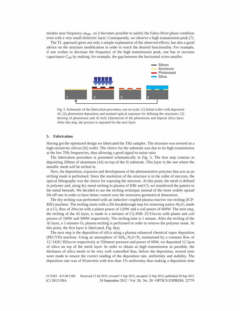
Fig. 5. Schematic of the fabrication procedure, not on scale. (1) Initial wafer with depositedAl; (2) photoresist deposition and masked optical exposure for defining the structures; (3)develop of photoresist and Al etch; (4)removal of the photoresist and deposit silica layer.After this step, the process is repeated for the next layer.
5. Fabrication
Having got the optimized design we fabricated the THz samples. The structure was erected on ahigh-resistivity silicon (Si) wafer. The choice for the substrate was due to its high transmissionat the low THz frequencies, thus allowing a good signal-to-noise ratio.
The fabrication procedure is presented schematically in Fig. 5. The first step consists indepositing 200nm of aluminum (Al) on top of the Si substrate. This layer is the one where themetallic mesh will be etched in.
Next, the deposition, exposure and development of the photosensitive polymer that acts as anetching mask is performed. Since the resolution of the structure is in the order of microns, theoptical lithography was the choice for exposing the structure. At this point, the mesh is definedin polymer and, using dry metal etching in plasma of HBr and Cl2 we transferred the pattern tothe metal beneath. We decided to use the etching technique instead of the more widely spreadlift-off one in order to have better control over the structures geometrical dimension.
The dry etching was performed with an inductive coupled plasma reactive ion etching (ICP-RIE) machine. The etching starts with a 20s breakthrough step for removing native Al2O3 madeat a Cl2 flow of 20sccm with a platen power of 120W and a coil power of 600W. The next step,the etching of the Al layer, is made in a mixture of Cl2/HBr 25/15sccm with platen and coilpowers of 100W and 500W respectively. The etching time is 1 minute. After the etching of theAl layer, a 5 minutes O2 plasma etching is performed in order to remove the polymer mask. Atthis point, the first layer is fabricated, Fig. 6(a).
The next step is the deposition of silica using a plasma enhanced chemical vapor deposition(PECVD) machine. Using an atmosphere of SiH4/N2O/N2 maintained by a constant flow of12/1420/392sccm respectively at 550mtorr pressure and power of 60W, we deposited 12.5μmof silica on top of the mesh layer. In order to obtain as high transmission as possible, thethickness of silica needs to be very well controlled thus, before the deposition, several testswere made to ensure the correct reading of the deposition rate, uniformity and stability. Thedeposition rate was of 81nm/min with less than 1% uniformity thus making a deposition time
#172483 - $15.00 USD Received 12 Jul 2012; revised 11 Sep 2012; accepted 12 Sep 2012; published 20 Sep 2012(C) 2012 OSA 24 September 2012 / Vol. 20, No. 20 / OPTICS EXPRESS 22779
of ca. 2h30min for the 12.5μm thick silica layer.
Fig. 6. Fabrication results. (a) Bottom layer; (b) top layer. The shadow of the bottom layercan be distinguished in the background.
Once the silica layer is deposited, the first steps are repeated with the only difference ofhaving to align the second exposure to the first one (see Fig. 6(b)). The last fabrication stepconsists in depositing a thin 200nm silica layer on top of the structure using the same recipe asfor the initial 12.5μm spacer.
6. Characterization
We characterized the fabricated samples using a T-Ray 4000 THz time-domain spectroscopysystem. For every sample 10.000 waveforms were recorded with the scan rate of 100 Hz andthe average of all the waveforms was then used for further investigation.
Fig. 7. Measured transmittance and reflectance intensity data. (a) Various pulse lengths and(b) their respective transmittance spectra showing the importance of correctly defining thecutting time-point; (c) transmittance (red) and reflectance (blue) for both the whole ABCdevice (solid lines) and C MTM layer (dashed). The averaged data for four devices and twomesh samples are presented.
Due to multiple reflections in the Si substrate the main pulse is closely followed by ripplesfrom multiple reflections in the thin silica layer, Fig. 7(a). The THz transient signals were cutafter careful analysis of the fourier transformed spectra. A too short pulse cut leads to significantloss of transmitted intensity, see points A, B, C in Fig. 7(a) and corresponding transmittancespectra in Fig. 7(b). On the other hand, in case of a too long pulse length (point D), the re-flected signal from the back of the substrate causes huge Fabry-Perot oscillations that make theinterpretation of the results difficult (see D line in Fig. 7(b)). Once the optimum cutting lengthwas obtained, the reference signal is cut accordingly. The transmittance measurements werenormalized to transmittance through the Si substrate with 12.5μm of silica characterized forreferencing. The reflected signal was normalized to the one of an Al mirror, considered to be aperfect reflector (|S11|2 � 100%) at THz wavelengths.
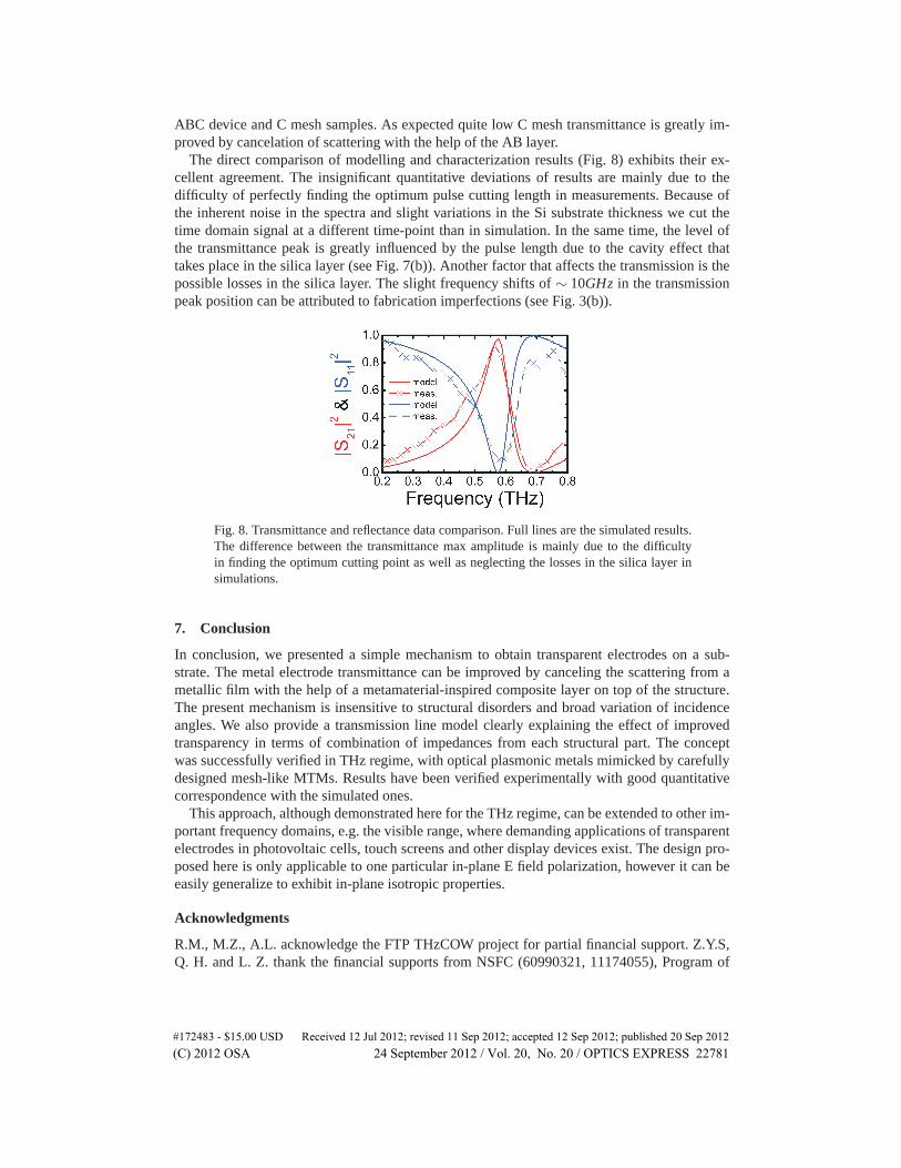
Figure 7(c) shows both normalized transmittance and reflectance spectra for the complete
#172483 - $15.00 USD Received 12 Jul 2012; revised 11 Sep 2012; accepted 12 Sep 2012; published 20 Sep 2012(C) 2012 OSA 24 September 2012 / Vol. 20, No. 20 / OPTICS EXPRESS 22780
ABC device and C mesh samples. As expected quite low C mesh transmittance is greatly im-proved by cancelation of scattering with the help of the AB layer.
The direct comparison of modelling and characterization results (Fig. 8) exhibits their ex-cellent agreement. The insignificant quantitative deviations of results are mainly due to thedifficulty of perfectly finding the optimum pulse cutting length in measurements. Because ofthe inherent noise in the spectra and slight variations in the Si substrate thickness we cut thetime domain signal at a different time-point than in simulation. In the same time, the level ofthe transmittance peak is greatly influenced by the pulse length due to the cavity effect thattakes place in the silica layer (see Fig. 7(b)). Another factor that affects the transmission is thepossible losses in the silica layer. The slight frequency shifts of ∼ 10GHz in the transmissionpeak position can be attributed to fabrication imperfections (see Fig. 3(b)).
Fig. 8. Transmittance and reflectance data comparison. Full lines are the simulated results.The difference between the transmittance max amplitude is mainly due to the difficultyin finding the optimum cutting point as well as neglecting the losses in the silica layer insimulations.
7. Conclusion
In conclusion, we presented a simple mechanism to obtain transparent electrodes on a sub-strate. The metal electrode transmittance can be improved by canceling the scattering from ametallic film with the help of a metamaterial-inspired composite layer on top of the structure.The present mechanism is insensitive to structural disorders and broad variation of incidenceangles. We also provide a transmission line model clearly explaining the effect of improvedtransparency in terms of combination of impedances from each structural part. The conceptwas successfully verified in THz regime, with optical plasmonic metals mimicked by carefullydesigned mesh-like MTMs. Results have been verified experimentally with good quantitativecorrespondence with the simulated ones.
This approach, although demonstrated here for the THz regime, can be extended to other im-portant frequency domains, e.g. the visible range, where demanding applications of transparentelectrodes in photovoltaic cells, touch screens and other display devices exist. The design pro-posed here is only applicable to one particular in-plane E field polarization, however it can beeasily generalize to exhibit in-plane isotropic properties.
Acknowledgments
R.M., M.Z., A.L. acknowledge the FTP THzCOW project for partial financial support. Z.Y.S,Q. H. and L. Z. thank the financial supports from NSFC (60990321, 11174055), Program of
#172483 - $15.00 USD Received 12 Jul 2012; revised 11 Sep 2012; accepted 12 Sep 2012; published 20 Sep 2012(C) 2012 OSA 24 September 2012 / Vol. 20, No. 20 / OPTICS EXPRESS 22781
Shanghai Subject Chief Scientist (12XD1400700) and MOE of China (B06011). A.A. acknowl-edges the FTP GraTer project for partial financial support.
#172483 - $15.00 USD Received 12 Jul 2012; revised 11 Sep 2012; accepted 12 Sep 2012; published 20 Sep 2012(C) 2012 OSA 24 September 2012 / Vol. 20, No. 20 / OPTICS EXPRESS 22782