A NEW TECHNIQUE FOR METAL OXIDE SURGE ARRESTERS FAILURE DIAGNOSTIC USING RETURN VOLTAGE MEASUREMENT ZULKURNAIN BIN ABDUL MALEK RESEARCH VOTE NO: 78228 FAKULTI KEJURUTERAAN ELEKTRIK UNIVERSITI TEKNOLOGI MALAYSIA 2009
Transcript
A NEW TECHNIQUE FOR METAL OXIDE SURGE ARRESTERS FAILURE
DIAGNOSTIC USING RETURN VOLTAGE MEASUREMENT
ZULKURNAIN BIN ABDUL MALEK
RESEARCH VOTE NO:
78228
FAKULTI KEJURUTERAAN ELEKTRIK
UNIVERSITI TEKNOLOGI MALAYSIA
2009
ii
ACKNOWLEDGEMENT
The author would like to acknowledge and thank Ministry of Higher Education for
providing the grant for this research.
iii
ABSTRACT
Due to their reliability and accuracy, many modern diagnostics based on
dielectric voltage response, such as polarization/depolarization current (PDC),
voltage decay (VD) and return voltage (RV) measurements, have been used in
monitoring ageing processes of metal oxide (MO) varistors, which is the main part of
a surge arrester. Among these diagnostics, recently, RV measurement (RVM) seems
to be an increasingly popular method as it has high sensitivity to the condition of
varistors and low sensitivity to disturbances in vicinity of the field measurements.
Nonetheless, the basic interpretation based on the RVM essential parameters – peak
RV, time-to-peak RV and initial slope of RV - provides insufficient information of
the MO varistors condition since they are inevitably dependent on the measuring
parameters such as the charging and discharging times as well as the test object
temperature. Hence, this project focuses on a new way in interpreting the RVM
parameters based on dielectric time constants analysis using an equivalent circuit of
varistor microstructure, namely the Maxwell-Model. In order to investigate the
ageing processes of MO varistors, two types of accelerated degradation techniques –
impulse and heat degradations – are systematically conducted on test samples.
Experimental results are presented and discussed in detail according to the
underlying physical mechanism. On the basis of this concept, a sensible ageing
parameter, p-factor, is used for better characterization of the ageing status of
varistors.
KEYWORDS: Metal oxide varistor, surge arrester, ageing, degradation, return
voltage measurement, dielectric time constant
iv
ABSTRAK
Disebabkan oleh keboleharapan dan ketepatannya, banyak diagnostik moden
berdasarkan pada respon voltan dalam dielektrik, seperti pengukuran
pengutuban/penyahkutuban arus (PDC), voltan penyusutan (VD) dan voltan balikan
(RV), telah digunakan dalam proses pemantauan penuaan varistor oksida logam
(MO) yang merupakan binaan utama penangkap pusuan. Di antara diagnostic-
diagnostik ini, kini, pengukuran RV (RVM) semakin meningkat digunakan kerana
mempunyai kepekaan yang tinggi terhadap keadaan varistor dan sensitiviti rendah
terhadap gangguan persekitaran proses pengukuran. Walaubagaimanapun,
penguraian asas berdasarkan pembolehubah penting RVM - puncak RV, masa-ke-
puncak RV dan kecerunan awal RV - tidak memberi maklumat yang cukup tentang
keadaan varistor MO kerana ia bergantung pada parameter pengukuran seperti
tempoh pengecasan and penyahcasan serta suhu objek. Oleh kerana itu, projek ini
fokus pada cara baru dalam mengurai pembolehubah RVM berdasarkan analisis
pemalar dielektrik masa dengan menggunakan litar yang sesuai untuk varistor
mikrostruktur - Maxwell-Model. Dalam proses untuk menyiasat penuaan varistor
MO, dua jenis teknik penuaan – secara aplikasi dedenyut dan pemanasan - dilakukan
secara sistematik pada sampel. Keputusan eksperimen tersebut dilaporkan dan
dibincangkan secara terperinci sesuai dengan mekanisma fizikal yang memdalam.
Atas dasar konsep ini, pembolehubah yang sesuai, p-faktor, digunakan untuk
menggambarkan dengan lebih baik status penuaan varistor.
v
TABLE OF CONTENTS
CHAPTER TITLE PAGE
ACKNOWLEDGEMENT iv
ABSTRACT v
ABSTRAK vi
TABLE OF CONTENTS vii
LIST OF TABLES x
LIST OF FIGURES xi
LIST OF SYMBOLS xiii
LIST OF ABBREVIATIONS xv
1 INTRODUCTION 1
1.1 Project Background 1
1.2 Problem Statement 2
1.3 Objective of Project 3
1.4 Scope of Project 3
1.5 Report Outline 3
2 LITERATURE STUDY 5
2.1 ZnO Varistor as Overvoltages Protective Device 5
2.1.1 Introduction 5
2.1.2 Microstructure and Common Equivalent
Circuit of ZnO Varistor 6
2.1.3 Electrical Characteristics of ZnO Varistor 7
2.1.4 Principle of Operation of ZnO Varistor 8
2.2 Degradation and Failure Mode of ZnO Varistor 9
vi
2.2.1 Electrical and Thermal Stresses 10
2.2.2 Failure Mode 11
2.3 ZnO Varistor Diagnostic Technique using Return
Voltage Measurements Method 11
2.3.1 Introduction 11
2.3.2 Return Voltage Measurements as a Reliable
Diagnostic Technique for ZnO-based
Protective Device 12
2.3.2.1 Basics of Return Voltage
Measurements Phenomenon 12
2.3.2.2 Previous Researches of Return
Voltage Measurements on Insulation
System 14
3 METHODOLOGY 16
3.1 Modeling ZnO Varistor based on Return Voltage
Measurements Phenomenon 16
3.1.1 Common Model of ZnO Varistor 16
3.1.2 Modeling ZnO Varistor based on Maxwell-
Model 17
3.1.3 Evaluation of Maxwell-Model Circuit 18
3.2 Laboratory Studies on ZnO Varistor Degradation 20
3.2.1 Test Sample Selection 20
3.2.2 Return Voltage Measurements 22
3.2.3 Total Leakage Current Measurements 24
3.2.3 1 mA Reference Voltage Measurements 26
3.2.4 Artificial Degradation of ZnO Varistor 27
3.2.4.1 Impulse Degradation 27
3.2.4.2 Heat Degradation 30
3.3 Interpretation of Return voltage Measurements 31
3.4 Project Flow Chart 32
4 DATA AND DISCUSSION 34
4.1 Introduction 34
vii
4.2 Results of Return Voltage Measurements 34
4.2.1 Sample A – Impulse Degradation 34
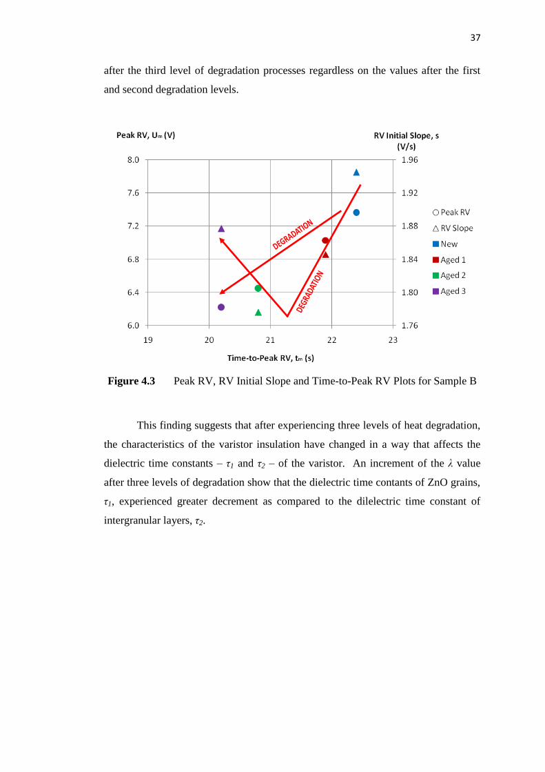
4.2.2 Sample B – Heat Degradation 36
4.2.3 Sample C – Impulse Degradation 38
4.2.4 Sample D – Heat Degradation 40
4.3 Results of Total Leakage Current Measurements 42
4.4 Results of 1 mA Reference Voltage Measurements 44
4.5 Results Comparison 45
5 CONCLUSION & SUGGESTION 48
5.1 Conclusion 48
5.2 Suggestion 49
REFERENCES 50
Appendices A - C 54
viii
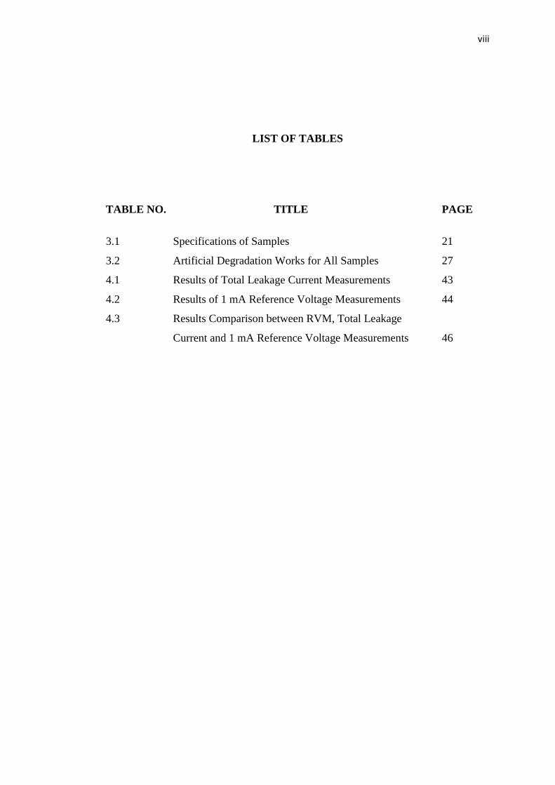
LIST OF TABLES
TABLE NO. TITLE PAGE
3.1 Specifications of Samples 21
3.2 Artificial Degradation Works for All Samples 27
4.1 Results of Total Leakage Current Measurements 43
4.2 Results of 1 mA Reference Voltage Measurements 44
4.3 Results Comparison between RVM, Total Leakage
Current and 1 mA Reference Voltage Measurements 46
ix
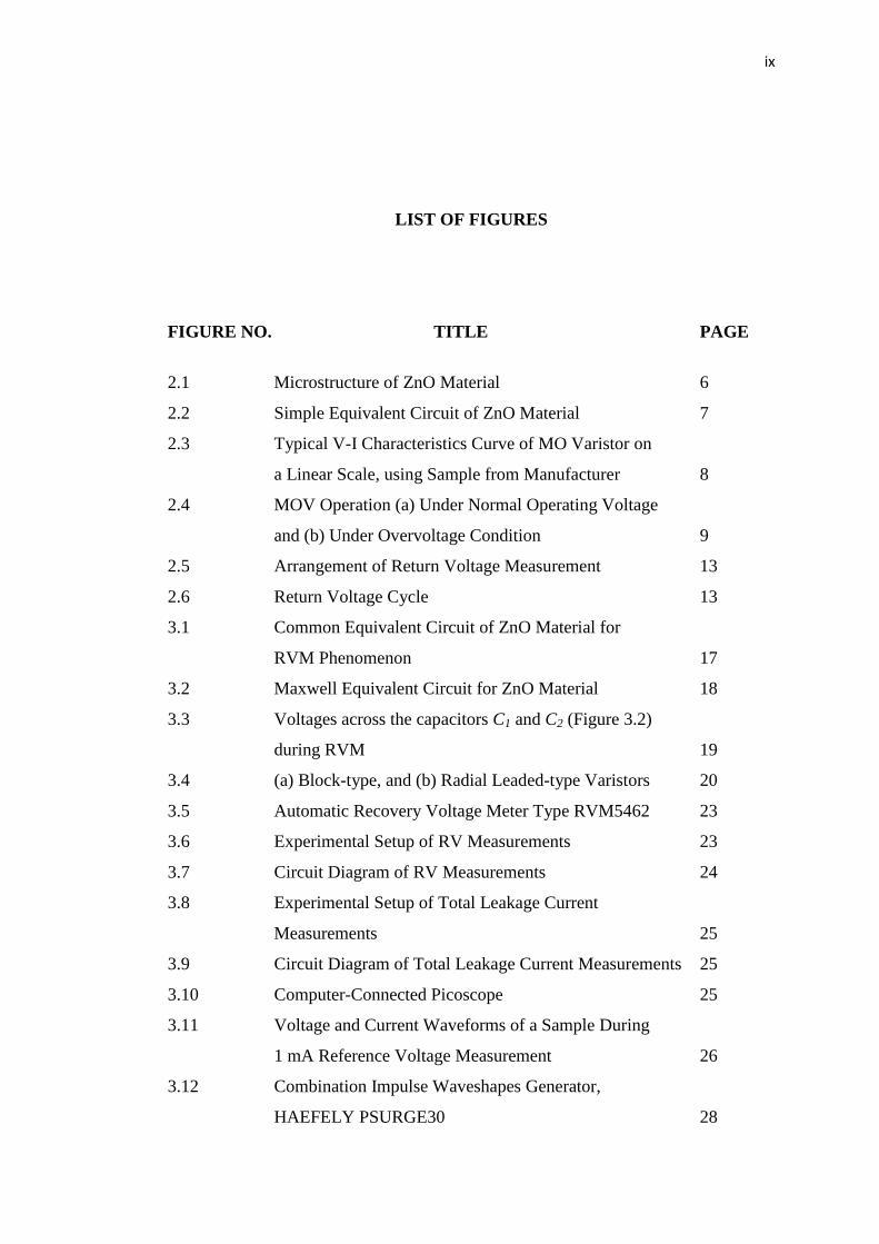
LIST OF FIGURES
FIGURE NO. TITLE PAGE
2.1 Microstructure of ZnO Material 6
2.2 Simple Equivalent Circuit of ZnO Material 7
2.3 Typical V-I Characteristics Curve of MO Varistor on
a Linear Scale, using Sample from Manufacturer 8
2.4 MOV Operation (a) Under Normal Operating Voltage
and (b) Under Overvoltage Condition 9
2.5 Arrangement of Return Voltage Measurement 13
2.6 Return Voltage Cycle 13
3.1 Common Equivalent Circuit of ZnO Material for
RVM Phenomenon 17
3.2 Maxwell Equivalent Circuit for ZnO Material 18
3.3 Voltages across the capacitors C1 and C2 (Figure 3.2)
during RVM 19
3.4 (a) Block-type, and (b) Radial Leaded-type Varistors 20
3.5 Automatic Recovery Voltage Meter Type RVM5462 23
3.6 Experimental Setup of RV Measurements 23
3.7 Circuit Diagram of RV Measurements 24
3.8 Experimental Setup of Total Leakage Current
Measurements 25
3.9 Circuit Diagram of Total Leakage Current Measurements 25
3.10 Computer-Connected Picoscope 25
3.11 Voltage and Current Waveforms of a Sample During
1 mA Reference Voltage Measurement 26
3.12 Combination Impulse Waveshapes Generator,
HAEFELY PSURGE30 28
x
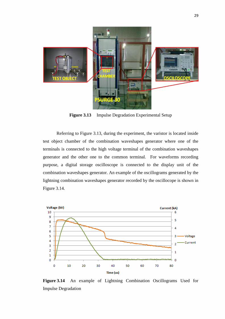
3.13 Impulse Degradation Experimental Setup 29
3.14 An example of Lightning Combination Oscillograms
Used for Impulse Degradation 29
3.15 Digimatic Drying Oven 30
3.16 Relationship Between p-factor and λ 32
3.17 Flow Chart of Project 33
4.1 Peak RV, RV Initial Slope and Time-to-Peak RV
Plots For Sample A 35
4.2 Relationship Between p-factor and λ=τ2/τ1 for
Sample A 36
4.3 Peak RV, RV Initial Slope and Time-to-Peak RV
Plots For Sample B 37
4.4 Relationship Between p-factor and λ=τ2/τ1 for
Sample B 38
4.5 Peak RV, RV Initial Slope and Time-to-Peak RV
Plots For Sample C 39
4.6 Relationship Between p-factor and λ=τ2/τ1 for
Sample C 40
4.7 Peak RV, RV Initial Slope and Time-to-Peak RV
Plots For Sample D 41
4.8 Relationship Between p-factor and λ=τ2/τ1 for
Sample D 41
4.9 Total Leakage Current Measurements for Sample D 42
4.10 Chart of Slope of Total Leakage Current Measurements
for All Samples 43
4.11 Chart of 1 mA Reference Voltage Measurements
for All Samples 45
4.12 Charts of Comparison for Each Technique for All
Samples 47
xi
LIST OF SYMBOLS
RIG - Resistance of intergranular layers
CIG - Capacitance of intergranular layers
RGRAIN - Resistance of grains
I - Current
K - Ceramic constant
V - Voltage
α - Non-linearity exponent
S1 - Switch 1
S2 - Switch 2
Up - Charging voltage
tc - Charging time
td - Discharging time
Um - Peak return voltage
tm - Time to reach return voltage
s - Initial slope of return voltage
Ro - Geometric resistance
Co - Geometric Capacitance
Rns - Resistance of n-th parallel branches
Cns - Capacitance of n-th parallel branches
εr - Relative permittivity
ρ - Specific resistance
τ1 - Dielectric time constant of material 1
τ2 - Dielectric time constant of material 2
C1 - Capacitance of material 1
C2 - Capacitance of material 2
ε1 - Permittivity of material 1
ε2 - Permittivity of material 2
xii
R1 - Resistance of material 1
R2 - Resistance of material 2
ρ1 - Specific resistance of material 1
ρ2 - Specific resistance of material 2
RL - Resistor of current limiter
VHV - Voltage on high voltage arm
VLV - Voltage on low voltage arm
oC - Degree Celsius
τ - Dielectric time constant
Ur - Return voltage
Us - Voltage after short circuit period
p-factor - New ageing parameter
xiii
LIST OF ABBREVIATIONS
UTM - Universiti Teknologi Malaysia
IVAT - Institute of High Voltage and High Current
ZnO - Zinc oxide
MOV - Metal oxide varistor
MO - Metal oxide
MOSA - Metal oxide surge arrester
VD - Voltage decay
PDC - Polarization/Depolarization current
RV - Return voltage
RVM - Return voltage measurement
V-I - Voltage-current
DC - Direct current
MCOV - Maximum continuous operating voltage
rms - Root mean square
Hz - Hertz
mm - Millimeter
kA - Kilo amperes
kV - Kilo volts
µs - Micro second
pF - Pico farad
J - Joule
xiv
LIST OF APPENDICES
APPENDIX TITLE PAGE
A Block-type Varistor Specifications 54
B Radial Leaded-type Varistor Specifications 55
C Printed Results from RVM 5462 56
1
CHAPTER 1
INTRODUCTION
1.1 Project Background
Surge protection devices are often used to protect power and electronic
equipment from the destructive transient overvoltage from lightning or other large-
magnitude surge. These devices are used to limit the overvoltage to a level which is
sufficiently safe for the equipment being protected by diverting the large current to
ground. The non-linearity characteristics of these devices depend on their material
composition. One type of non-linear devices is known as metal oxide varistor
(MOV). MOV is a ceramic device with highly non-linear electrical characteristics;
similar to those of a back-to-back diode, and has been used for low voltage
application (below 1 kV). For higher voltage application that is above 1 kV the
protection device is usually known as metal oxide surge arrester (MOSA) which may
consists of several MOV blocks. Due to its high nonlinear characteristics, these
devices have high energy absorption capability which is a good characteristic for an
overvoltage suppressor.
However, these nonlinear characteristics can be degraded by the effects of
electrical and thermal stresses as well as chemical reactions with the surrounding
material. Usually, the thermal stress is considered as effect due to the temperature
rise of the metal oxide materials subsequent to the discharge of high energy surges.
While, the electrical stress may be the effects of voltage stress by its own operating
2
voltage at ambient temperature or by high current stress due to overvoltages
occurrence.
In the past, many investigations of several non-destructive diagnostic
techniques have been conducted for reliable condition assessment of the ageing of
MOSA. These diagnostic techniques include the standard 1mA reference voltage,
lightning impulse discharge residual voltage, voltage decay (VD), polarization or
depolarization current (PDC) and Return Voltage (RV) measurements. The modern
diagnostic techniques based on dielectric response such as VD, PDC and RV
measurements, have also been used to evaluate insulating materials such as cables
and transformers [1-4].
Among these modern diagnostic techniques, recently, the return voltage
measurement (RVM) seems to be increasingly used as a reliable diagnostic method
in monitoring the ageing process of the metal oxide materials due to its high
sensitivity to smaller degrees of degradation [5]. In addition, RVM has low
sensitivity to disturbances by external noise, a situation that is auspicious for in-field
measurements [6].
1.2 Problem Statement
RVM method is a good approach to attain the information of insulating
components condition for devices such as ZnO varistor (under normal operating
mode). Due to less sensitive to disturbances, the measurements are reliable and also
reproducible, at least with regard to the collection of the data. Unfortunately, in the
past, not all RVM interpretation methods suggest correct insulation components
condition information because of unreliable diagnosis parameters and inaccurate
RVM data interpretation approach. Hence, this project focus on investigation of an
accurate and correct way to interpret RVM data of ZnO varistor in order to obtain
real physical condition of the ZnO insulation.
3
1.3 Objective of Project
There are two main objectives that have been achieved in this project:
To model the equivalent circuit of ZnO varistor according to RVM
phenomenon using Maxwell multilayer dielectric circuit.
To investigate reliable interpretation of ZnO degradation process using
RVM method.
1.4 Scope of Project
The main scope of this project is to study the diagnostic tecnique of ZnO
varistor based on RVM method which includes:
Study of behaviour and characteristics of metal oxide material;
Study of theory, principles and interpretation of RVM;
Evaluation of metal oxide material using multilayer dielectric approach –
Maxwell-Model;
Experimental works of ageing investigation on MOV using RVM
method; and
Results validation by comparison with total leakage current and 1 mA
reference voltage measurements.
1.5 Report Outline
This report is divided into five chapters. Generally, some basic principles,
theories, equations, previous researches’ references, experimental result and
discussions are discussed included in these chapters based on the contents
requirements of each chapter.
4
In chapter 1, the author has included the project overview and the main
objectives of conducting this project. Chapter 2 presents some background
information of the project, such as the description of ZnO varistor as overvoltage
protective device, and RVM as ZnO varistor diagnostic technique. This chapter
briefly explains the ZnO varistor structure, common equivalent circuit and electrical
characteristics as well as the importance of conducting a research on its diagnostic
technique. At the end of the chapter, the author summarizes the current research
works done by other researchers and of course their valuable recommendations.
Chapter 3 presents the methodologies of modeling ZnO varistor as well as the
experimental procedures of carrying out the RV measurements. These are presented
in a flow chart form together with a brief explanation. The RVM interpretation
methods are discussed at the end of this chapter. Then, data and discussion are
covered in Chapter 4.
Finally, Chapter 5 summarizes all the works and studies that had been
presented in the previous four chapters. Besides, some future works are suggested at
the end of the chapter.
5
CHAPTER 2
LITERATURE STUDY
2.1 ZnO Varistor as Overvoltage Protective Device
2.1.1 Introduction
ZnO varistor plays an important role in avoiding any electrical or electronic
equipment failure caused by dangerous, damaging transients or lightning surges.
ZnO varistors are permanently connected from line to ground near the equipment
being protected. Equipment failure can be minimized from better surge protection,
that is highly desirable in order to promise good overall system reliability. The
protection level of ZnO varistor depends on the withstand requirements such as high-
energy absorption capability, current withstand and voltage withstand levels. A
conventional varistor is an insulator or a very poor conductor at nominal operating
condition so that it can prevent power follow current flowing through it. At the
occurrence of a surge, it must be able to transform to a relatively good conductor
(with some equivalent resistance) and diverting safely thousands of amperes of
current to the ground. After the dissipation of surge current, a good varistor should
return back to the non-conducting mode with its original V-I characteristics restored.
6
2.1.2 Microstructure and Common Equivalent Circuit of ZnO Varistor
MOV has highly non-linear resistance which is primarily zinc oxide added
with other materials. Conductive zinc oxide grains separated by boundaries that
form semiconductor junctions, just like a semiconducting diode. A metal oxide
varistor microstructure is equivalent to combinations of millions series and parallel
semiconducting diodes. Figure 2.1 shows the conduction mechanism in a metal
oxide varistor. As shown in the figure, the electrical behaviour of the metal oxide
varistor results from the number of microvaristors connected in series or in parallel.
Energy absorbers are provided for each microvaristor in form of grains with
optimum thermal contact which allow high absorption of energy and thus
exceptionally high surge current capability [7]. The resistance is very high with low
voltage across the boundaries and vice versa.
Figure 2.1 Microstructure of ZnO material
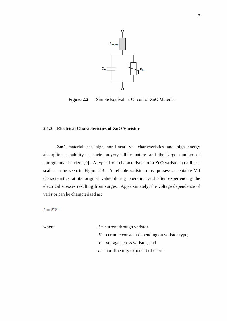
The simple equivalent model to describe the ZnO material in terms of
electrical components is an RIG-CIG parallel circuit in series with another resistor,
RGRAIN and an inductance. RIG is defined as a highly non-linear resistor with
increasing voltage. Similar to non-linear behaviour of intergranular layers of ZnO
material, we have the capacitance, CIG. RGRAIN is the resistance of conducting ZnO
grains. The capacitance of ZnO grains is very small and can be neglected and the
series inductance represents the inductance of the arrester body which is only
considered for the steep response currents. The resulting equivalent circuit modelled
is as shown in Figure 2.2 [8].
7
Figure 2.2 Simple Equivalent Circuit of ZnO Material
2.1.3 Electrical Characteristics of ZnO Varistor
ZnO material has high non-linear V-I characteristics and high energy
absorption capability as their polycrystalline nature and the large number of
intergranular barriers [9]. A typical V-I characteristics of a ZnO varistor on a linear
scale can be seen in Figure 2.3. A reliable varistor must possess acceptable V-I
characteristics at its original value during operation and after experiencing the
electrical stresses resulting from surges. Approximately, the voltage dependence of
varistor can be characterized as:
where, I = current through varistor,
K = ceramic constant depending on varistor type,
V = voltage across varistor, and
α = non-linearity exponent of curve.
8
Figure 2.3 Typical V-I Characteristics Curve of MO Varistor on a Linear Scale,
using Sample from a Manufacturer [7]
A V-I characteristic for a typical resistor is linear and has the value of α = 1.
Generally, as the value of α increased, the characteristics of the varistor are
approaching the ideal one. For a modern design of varistor, typical range of the α
value is between 30 and 100 [9].
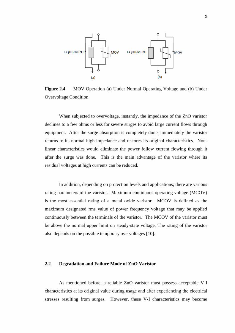
2.1.4 Principle of Operation of ZnO Varistor
MOVs protect any equipment revealable to permanent damage from rapid,
long term lightning strikes. They must be installed closely to the equipment being
protected. Figure 2.4 shows the operation of MOV under normal operating voltage
and under overvoltage condition. As shown in the figure, the MOV act as the
protection component of the equipment. Under normal operation, MOV has very
high impedance up to several mega ohms and it can be considered as open circuit.
Therefore, all of the current in circuit will flow through the equipment and bypassing
the MOV.
9
Figure 2.4 MOV Operation (a) Under Normal Operating Voltage and (b) Under
Overvoltage Condition
When subjected to overvoltage, instantly, the impedance of the ZnO varistor
declines to a few ohms or less for severe surges to avoid large current flows through
equipment. After the surge absorption is completely done, immediately the varistor
returns to its normal high impedance and restores its original characteristics. Non-
linear characteristics would eliminate the power follow current flowing through it
after the surge was done. This is the main advantage of the varistor where its
residual voltages at high currents can be reduced.
In addition, depending on protection levels and applications; there are various
rating parameters of the varistor. Maximum continuous operating voltage (MCOV)
is the most essential rating of a metal oxide varistor. MCOV is defined as the
maximum designated rms value of power frequency voltage that may be applied
continuously between the terminals of the varistor. The MCOV of the varistor must
be above the normal upper limit on steady-state voltage. The rating of the varistor
also depends on the possible temporary overvoltages [10].
2.2 Degradation and Failure Mode of ZnO Varistor
As mentioned before, a reliable ZnO varistor must possess acceptable V-I
characteristics at its original value during usage and after experiencing the electrical
stresses resulting from surges. However, these V-I characteristics may become
10
degraded due to various electrical stresses and environmental pollution.
Consequently, monitoring the varistor condition becomes more complicated while in
operation [10].
2.2.1 Electrical and Thermal Stresses
There are two factors that influence the degradation of MO varistor; thermal
and electrical stresses. Typically, the thermal stresses are considered as effects of the
solar radiation and pollution on the arrester housing and also due to the temperature
rise of the MO element subsequent to the discharge of high energy surges.
Meanwhile, the transient electrical stresses are accounted by the lightning, switching
and temporary overvoltages effects [11].
It is believed that ion migration found a strong basis of existence based on the
evidence of measurements of thermally stimulated currents of stressed MO varistors.
The potential barrier height at MO grain is modified by charge migration due to the
degradation of varistors. The charge migration is controlled by the varistor electric
field and temperature.
From previous studies, it is known that degradation mainly affects the pre-
breakdown region of the V-I curve and results in increased leakage currents. The
degradation is concluded to be a grain boundary related phenomenon since the pre-
breakdown region is grain boundary controlled. A stressed MO varistor also
believed to change its microstructure when it is preheated to certain temperatures
depending on its previous degree of degradation and resulting in the change in its
capacitive and resistive characteristics [10].
11
2.2.2 Failure mode
The performance of varistor could be affected by rapid higher overvoltages
activities throughout the time of their services. Damage on varistors can be seen as
cracks on the MOV surface or defect surfaces resulting from stresses.
Before installing varistors to a system, one of essential considerations besides
their rating, is the thermal effect, either due to environmental aspects or lightning
surges. The temperature of varistors is increased with the ambient temperature or
energy absorbed by them. This proliferation of temperature cause additional heat to
the varistors. A phenomenon called thermal runaway takes place when the
temperature exceeds the thermal capability of the metal oxide valve element.
Thermal runaway is a phenomenon that occurs whenever the MOV disc is
exposed to elevated temperature during operation and begins to conduct – allow
current flowing through it - at voltage below the rated clamping or switching voltage.
Eventually, this phenomenon leads to physical destruction of the MOV component.
Thus, some adequate laboratory tests on MOV performance are required to ensure
good reliability of the varistor in service [12].
2.3 ZnO Varistor Diagnostic Technique Using RVM Method
2.3.1 Introduction
Since the degradation of ZnO varistors results in thermal runaway and leads
to a short circuit, the condition evaluation of the ZnO insulation under normal
operating voltage becomes significant to ensure their reliability in service. Several
diagnostic techniques such as the standard 1mA reference voltage, lightning impulse
discharge residual voltage, voltage decay (VD), polarization or depolarization current
(PDC) and Return Voltage (RV) measurements, have been used to investigate the
12
insulation condition of ZnO varistors. Among these techniques, it has been proved
that RVM technique is the most sensitive technique to detect smaller changes in ZnO
insulation condition and furthermore it is insusceptible to field noises during the
measurements [5, 6].
2.3.2 RVM Method as Reliable Diagnostic Technique for ZnO-based
Protective Device
Since a few years back, RVM method is a favorable modern diagnostic
technique for MO-based material since it sensitively detects smaller degrees of
degradation. Due to its reproducibility, this method can also be used for on-site
measurements [5]. Better assessment on the insulation performance, condition and
degradation can be investigated and evaluated using this method.
2.3.2.1 Basics of RVM Phenomenon
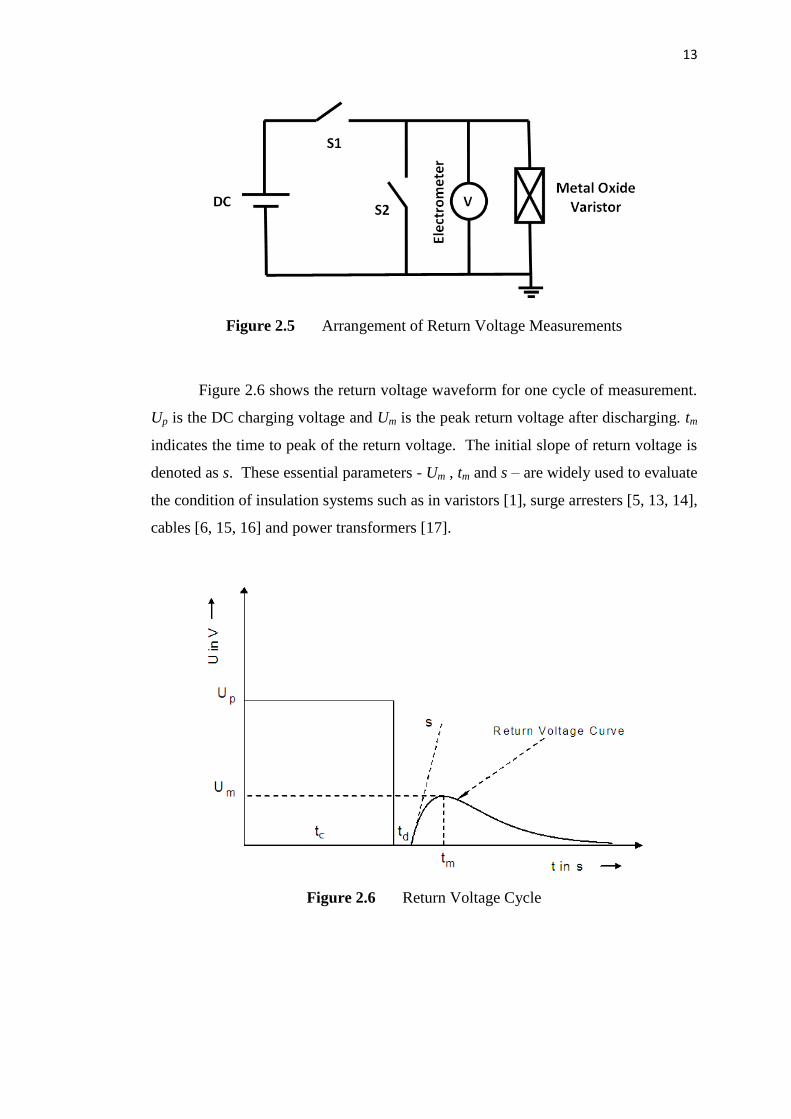
Arrangement of RVM is shown in Figure 2.5. Based on the figure, with only
switch S1 closed, RV measurement starts by charging a MO varistor with a DC
voltage, Up for a pre-selected time known as the charging time, tc. This DC voltage
must be much lower than the operating voltage of the varistor, so that the varistor is
acting like an insulator. Next step is discharging the varistor by short circuiting both
varistor’s terminals to the ground for a short time period called the discharging time,
td with switch S2 closed and switch S1 is opened. Finally, with switch S1 and S2
opened, the open circuit voltage that built up across the varistor is measured using an
electrometer which is a high impedance measuring system. This build up voltage –
the return voltage - is widely used to characterize the condition of the varistor being
measured.
13
Figure 2.5 Arrangement of Return Voltage Measurements
Figure 2.6 shows the return voltage waveform for one cycle of measurement.
Up is the DC charging voltage and Um is the peak return voltage after discharging. tm
indicates the time to peak of the return voltage. The initial slope of return voltage is
denoted as s. These essential parameters - Um , tm and s – are widely used to evaluate
the condition of insulation systems such as in varistors [1], surge arresters [5, 13, 14],
cables [6, 15, 16] and power transformers [17].
Figure 2.6 Return Voltage Cycle
14
2.3.2.2 Previous Researches of RVM on Insulation System
Previous findings [16, 18] found that the RVM method is a good tool to
assess the condition of oil-paper insulation systems as it can provide a strong
correlation between the progress of moisture content and ageing in the insulation and
the polarization spectra. The ageing processes in paper-oil insulated high voltage
cables and transformers can reliably be monitored by using this method due to its
capability in detecting the changes in dielectric properties of composite insulations.
A reliable interpretation of correlation between the slope of the return voltage
and period of ageing of the polymeric insulated cables, had also been proven [15].
As described in previous publications [5, 13, 14], the maximum Um and the
corresponding central time constant generally tend to decrease after a MO-based
device experiences several current impulses. The effect of multipulse lightning
current on MO material characteristics is claimed to be much more severe than single
lightning pulse. Furthermore, the decrease in the central time constant maybe due to
the increment of MO conductivity after undergoing ageing processes [14].
Since a ZnO varistor behaves almost like an insulator at normal operating
voltage which is below its rated voltage, the polarization and depolarization of
dipoles within the MO material as well as on the charging and discharging of grain
boundaries and space effects can be monitored by RVM [5]. Therefore, RVM may
be used as a good indicator for the ageing level of the MO. Yet, interpretation of the
RVM data and results based on these three basic ageing parameters – Um, tm ans s –
suggested inaccurate condition of ZnO material since those parameters are
influenced by DC charging voltage, Up, charging time, tc, discharging time, td and
test object temperature [19] during the measurements.
Recently, the interpretation of RVM data has been studied and proven [6, 16,
20] to be a good indicator to insulation ageing such as in power cables based on
dielectric time constant method using Maxwell dielectric quivalent circuit. This
method seems plausible in monitoring the condition of the insulation system in
15
power cable which is a multi-layer insulation system – paper and oil – since it is
independent from the Up, tc, td as well as surrounding temperature during the RV
measurements. Based on the RV phenomenon, a physically adequate equivalent
circuit of insulator has been developed to describe the insulation system and being
used to deliver the accurate data about the dielectric properties which is a good
indicator of ageing process. Since the ZnO structure consists of two different
dielectric materials which are zinc oxide grain and intergranular layer, and behave as
an insulator below its normal operating voltage, this interpretation method can be
applied in evaluating the condition of the varistor.
16
CHAPTER 3
METHODOLOGY
3.1 Modelling ZnO Varistor based on RVM Phenomenon
3.1.1 Common Model of ZnO Varistor
In the past, the insulation of MO material under normal operating condition is
commonly represented by an equivalent model consisting the insulation resistance,
Ro and geometric capacitance, Co with a number of additional R-C branches [21] as
shown in Figure 3.1. The individual polarization process is represented by these R-C
parallel branches with their time constant RnsCns and is treated independent to each
other. The representation of the polarization processes using R-C parallel branches
in line with the theory of distributed relaxation times to predict the response of the
insulation, which hardly follows ideal Debye behaviour [21]. The displacement
current in the insulation is determined by the geometric capacitance Co, internal
resistance Ro and the R-C pairs with the associated time constant and the conduction
current is only by the internal resistance Ro.
Based on the equivalent circuit, a numerical fit approach is often used in the
analysis of RV curves or polarization/depolarization currents over time. These
numerical values, Rns and Cns, are calculated according to exponential fitting of the
measured relaxation or depolarization current [21] and being used to characterize the
condition of the ZnO varistor. However, these ‘best fit’ numerical values are only a
purely formal description regardless of any physical meaning of ZnO insulation.
17
Figure 3.1 Common Equivalent Circuit of ZnO Material for RVM Phenomenon
3.1.2 Modelling ZnO Varistor Based On Maxwell-Model
As discussed in Section 2.1.2, the microstructure of ZnO varistor consists of
two different dielectric properties - ZnO grains and intergranular layers - that is
equivalent to combinations of millions series and parallel semiconducting diodes.
Hence, as these dielectrics have different compositions with different relative
permittivity, εr and specific resistance, ρ [8, 22], an adequate equivalent circuit for a
ZnO varistor - multilayer dielectric - is the Maxwell-Model with two R-C parallel
circuits in series as shown in Figure 3.2. The model is relevant to describe the
boundary polarization process in the ZnO materials and more appropriate since it
closely reproduces the real physical meaning of the condition of the ZnO material.
Consequently, instead of only considering the molecular polarization processes
during RV measurements, it also shows the phenomenon of boundary polarization
which is primarily involving volume conductive processes.
When a multilayer dielectric is subjected to a DC voltage, which leads to a
dielectric polarisation, capacitive voltage starts to distribute within both layers and
continuously changes into a resistive voltage distribution. Electric charges migrate
between layers and in part accumulate at interface boundaries, where local electric
fields are generated by the charges to necessarily obey the continuity equation for the
current density. After the charging voltage is removed, within the short circuit
period, depolarisation of the insulation starts where the charges at the external
18
electrodes are released according to the dielectric layers time constants, ε1ρ1 and ε2ρ2.
After this period, as the free charges have vanished, the dielectric depolarisation
continues and results in the previous bound charges to become free charges.
Consequently, a so-called ‘return voltage’ occurs across the multilayer dielectric due
to the built-up of the free charges [23, 24].
Figure 3.2 Maxwell Equivalent Circuit for ZnO Material
3.1.3 Evaluation of Maxwell-Model Circuit
Phenomenon of RV in a multilayer dielectric is analyzed on the basis of the
Maxwell-Model [23] as shown in Figure 3.3. Referring to the figure, at the presence
of DC voltage in multilayer dielectric during charging time, tc, a capacitive voltage
division of the DC charging voltage, Up occurs between voltages across capacitor C1,
U1, and capacitor C2, U2. Gradually, this capacitive voltage changes into an ohmic
division according to resistances of R1 and R2. Then, during short circuit period –
discharging time, td – intermigration of charges take place, where both of the
capacitors voltages decrease simultaneously with a time constant τ until these
voltages are identical. After the short circuit is released, the voltages across both of
the capacitors decrease independently depending on individual time constants, τ1 and
τ2, resulting in voltage build up, Ur across the dielectric.
19
Figure 3.3 Voltages across the capacitors C1 and C2 (Figure 3.2) during RVM
For an insulation material, the dielectric time constant, τ is proportional to the
product of relative permittivity, εr and the specific resistance, ρ, (εrρ) and it is
independent of the geometrical dimensions and the shape of the dielectric [25]. The
time constant is sensitively affected by any changes of ρ and εr [17]. Hence, for a
parallel R-C circuit, the corresponding dielectric time constant, τ equals to RC
(τ=RC) where it exclusively determines the dielectric properties of the insulation.
For the equivalent circuit shown in Figure 8, the return voltage, Ur equation
for a multilayer dielectric is given as,
The voltage across both of the capacitors after charging time, tc and
discharging time, td is as follows,
20
where τ is the time constant under short circuit of the dielectric system and λ is the
dielectric constants ratio, τ2/τ1. Obviously, return voltage equation, Ur (t) has a
complex dependence on Us factor of the dielectric.
Based on the equations above, dielectric constant τ2 is greater than τ1 due to
the dielectric properties of element R1-C1 is greater than element R2-C2. For zinc
oxide material, element R1-C1 represents the zinc oxide grains which are highly
conductive component and element R2-C2 represents the intergranular layers, the
non-conducting component.
3.2 Laboratory Studies on ZnO Varistor Degradation
3.2.1 Test Sample Selection
For experimental works in this project, two types of new ZnO varistor from
different manufacturers were used. Two varistors from each manufacturer were
chosen as project samples named as sample A, B, C and D. Sample A and B are
block-type varistors while sample C and D are radial leaded-type varistors. Figure
3.4 shows the block-type and radial leaded-type varistors used in the project and
details of these varistors are presented in Table 3.1. Full specifications of these
varistors can be referred to Appendices A and B.
(a) (b)
Figure 3.4 (a) Block-type, and (b) Radial Leaded-type Varistors
21
Table 3.1 Specifications of Samples
Varistor Type Block Radial Leaded
Specification
Diameter: 40mm
Height: 21mm
Voltage Rating, AC: 3kV
Current Rating: 10kA
Max Continuous Operating
Voltage: 2.55kV
Voltage at 1mA: 4kV
Lightning Impulse Residual
Voltage at:
5kA - 8.3kV
10kA – 8.8kV
20kA – 10.3kV
Diameter: 14mm
Voltage Rating, AC: 1000V
Voltage Rating, DC: 1200V
Peak Pulse Current at 8/20µs: 4.5
kA
Max Clamping Voltage at 8/20µs:
2700V
Max Transient Energy 10/1000µs:
220J
Capacitance: 130pF
Voltage at 1mA Max: 1800V
Voltage at 1mA Min: 1425V
In choosing the test samples, several characteristics of the devices must be
considered in order to satisfy the experimental work requirements. Some
characteristics of varistor are defined as follows:
Maximum Continuous Operating Voltage (MCOV) - Maximum AC
voltage applied continuously between the terminals of the varistor
1 mA Reference Voltage - Voltage required for 1 mA current flows
through varistor
Maximum Clamping Voltage – Maximum voltage across the varistor
terminals when a lightning current impulse is applied
Nominal Discharge Current – Peak value of lightning current impulse,
which is used as varistor classification
22
Energy Absorption Capability – Maximum level of energy subjected into
varistor at which it can still cool down back to its normal operating
temperature
3.2.2 Return Voltage Measurements
All the experimental works in this project were performed in the High
Voltage Laboratory of the Institute of High Voltage and High Current (IVAT) in
Universiti Teknologi Malaysia (UTM) Skudai. In this project, single cycle of RV
measurements were conducted on each sample before and after experiencing
degradation processes. Prior to any RV measurement, all test samples were firstly
short circuited to ground for at least 24 hours to eliminate any remaining charges
from previous tests. These previous effects normally influence the measurement
accuracy and reproducibility [1].
The measurements of the return voltage were carried out using a commercial
automatic recovery voltage meter, type RVM 5462 by TEXTEX Instruments, as
shown in Figure 3.5. As described in Section 2.3.2.1, all the RVM processes
including polarization (charging process), depolarization (discharging process),
relaxation process and return voltage measurement, are automatically carried out by
this portable microprocessor-controlled RVM meter. For each measurement, the
essential parameters of RVM - Um, tm and s – were printed out (refer Appendix C) by
its internal printer and the points of measured RV curves were recorded manually
(not printable).
The settings of the RVM meter for each measurement can be referred as
below:
Charging DC voltage: 500 V (Sample A and B)
200 V (Sample C and D)
Charging time, tc: 600 s
Discharging time, td: 60 s
tc/td ratio: 10
23
Figure 3.5 Automatic Recovery Voltage Meter Type RVM 5462
In this project, the charging and discharging time ratio, tc/td for RV
measurements was not the same as previous researches, typically, tc/td equal to 2 [1,
13, 14], 450 [19, 23] or 900 [20] due to the fact that the new essential RV curve
parameter, p-factor (presented in Section 3.3), which is to be obtained by these
procedures is independent from the tc/td ratio [20]. The experimental setup of RV
measurement is shown in Figure 3.6. Figure 3.7 shows the circuit diagram of the
measurement. Referring to Figure 3.6, during the RVM, one terminal of the varistor
is connected to the high voltage cable of the RVM meter (red crocodile clip) and
another terminal is grounded (black crocodile clip).
Figure 3.6 Experimental Setup of RV Measurements
24
Figure 3.7 Circuit Diagram of RV Measurements
3.2.2 Total Leakage Current Measurements
The total leakage current method was used as one of the reference methods
for RVM results justification. Comparison between these methods was discussed
detail in Chapter 4. The total leakage current measurements were performed for all
test samples before and after each of degradation levels. The experimental setup and
circuit diagram of the measurement can be respectively referred to in Figure 3.8 and
Figure 3.9. The circuit consists of a step-up transformer, a resistance current limiter
(RL = 10 MΩ), a capacitive divider (VHV/VLV = 5112), a measuring resistance of 10
kΩ (resistive shunt) and a computer-connected Picoscope (refer Figure 3.10).
With the use of a Picoscope, for each sample, the rms value of total leakage
current through the varistors was measured as the AC voltage source is increased
gradually. These rms values of supply voltage and total leakage current were
recorded and plotted. Detail discussions on the total leakage current measurements
were presented in Chapter 4.
25
Figure 3.8 Experimental Setup of Total Leakage Current Measurement
Figure 3.9 Circuit Diagram of Total Leakage Current Measurements
Figure 3.10 Computer-Connected Picoscope
26
3.2.3 1 mA Reference Voltage Measurements
The reference voltage is defined as the required voltage across varistor
terminals to pass a specific reference current through it [26, 27]. Typically the
reference current is in the range of 1 mA to 10 mA and rather close to the breakdown
point in the breakdown region of the V-I characteristics. At this point, the total
leakage current of the varistor consists of larger resistive component compared to the
capacitive component. The resistive leakage current component is claimed to give
significant changes in the change of the varistor characteristics due to ageing
processes [28].
In this project, 1 mA of current flowing through the samples is also used as
the reference current. Experimental setup for the 1 mA reference current
measurement is similar to that for the total leakage current measurement as shown in
Figure 3.8. However, the procedures on data collection were quite different. During
each measurement, the voltage across the varistor is increased slowly until the value
of total leakage current flowing through the varistor at the instant when the voltage is
at its peak value, is equal to 1 mA (refer to Figure 3.11). This rms value of voltage,
called as the reference voltage, is recorded. The effect of varistor degradation
processes on the reference voltage was investigated in this project and is discussed in
Chapter 4.
Figure 3.11 Voltage and Current Waveforms of a Sample during 1 mA Reference
Voltage Measurement
27
3.2.4 Artificial Degradation of ZnO Varistor
There are two types of artificial degradation works that have been conducted
on the samples in this project which are impulse and heat degradation techniques.
All the degradation works are summarized in Table 3.2.
Table 3.2 Artificial Degradation Works for All Samples
Degradation
Technique Sample
Degradation
Level Degradation Works for Each Level
Impulse
A
1st
10 times 8.5kV-5kA Lightning Combination
Wave at 1 min intervals 2
nd
3rd
C
1st
5 times 3.6kV-2.5kA Lightning
Combination Wave at 1 min intervals 2
nd
3rd
Heat
B
1st
120 hours / 5 days at 120˚C 2nd
3rd
D
1st
120 hours / 5 days at 120˚C 2nd
3rd
3.2.4.1 Impulse Degradation
A combination wave generator of 1.2/50µs and 8/20µs lightning waveshapes,
HAEFELY PSURGE30 (refer Figure 3.12), which is accessible in Institute of High
Voltage & High Current (IVAT), was used for the impulse degradation works.
Specifications of the combination waveshapes generator can be referred as below:
28
Model: HAEFELY Surge Generator PSURGE30
Maximum energy: 4.9 kJ
Open circuit output voltage: 3-30 kV ± 10 %
Voltage Front time: 1.2 μs ± 30 %
Voltage Time to half value: 50 μs ± 20 %
Short circuit output current: 1.5-15 kA ± 20 %
Current Front time: 8 μs ± 20 %
Current Time to half value: 20 μs ± 20 %
Dynamic impedance: 2 Ω ± 0.25Ω
Impulse capacitor: 9 μF ± 10 %
Impulse interval: min. 10 s
Sample A (block-type) and C (radial leaded-type) experienced three levels of
impulse degradation. For sample A, each level consists of ten lightning combination
impulses at 8.5 kV-5 kA with an interval of one minute. While, each degradation
level of sample C consists of five lightning combination impulses at 3.6 kV-2.5 kA
with one minute interval. The experimental setup of the impulse degradation is