A new vibrational technique for measurement of stress variations in thin films A thesis submitted by Sreten Askraba B.Sc.(Eiec. Eng.) for the degree of Doctor of Philosophy Optical Technology Research Laboratory School of Communications and Informatics Victoria University Melbourne May, 1999
Transcript
A new vibrational technique for measurement of stress variations in
thin films
A thesis submitted
by
Sreten Askraba B.Sc.(Eiec. Eng.)
for the degree of
Doctor of Philosophy
Optical Technology Research Laboratory School of Communications and Informatics
Victoria University Melbourne May, 1999
FTS THESIS 530.4275 ASK 30001005536844 Askraba, Sreten A new vibrational technique for measurement of stress variations in thin films
This PhD thesis is dedicated to my parents
1 1
Declaration
I, Sreten Askraba, declare that the thesis tided,
"A new vibrational technique for measurement of stress variations in thin films"
is my own work and has not been submitted previously, in whole or in part, in
respect of any other academic award.
Sreten Askraba
dated the 17* May, 1999
1 1 1
Acknowledgments
There are a number of people to whom I wish to thank for assistance
throughout my PhD study. Firstiy I would like to thank my PhD supervisor
Professor David Booth for giving me the opportunity and having confidence in my
ability, his guidance, invaluable advice and assistance given throughout my course
of study.
I am very grateful to Dr Tranxuan Danh from Department of Mechanical
Engineering, Victoria University, for helpful assistance in using ANSYS 5.3 Finite
Element Modeling software. I would like to thank my fellow post-graduate students
for their friendship and help when it was required.
Without the help of the technical staff my project would have not been a
success. Therefore I would like to thank Mr. Alex Shelamoff for his assistance with
the design of electronic detection circuit. From the mechanical workshop I would
like to thank Mr. Mark Kivienen, and Mr. Donald Ermel for their helpful
consultation, designing and construction of necessary parts for the vacuum system.
In addition I would like to thank all the other academic, technical and administrative
staff from the Department of Applied Physics, Victoria University.
I V
Abstract
A survey of thin films deposited by standard techniques (electro-
deposition, chemical deposition, sputtering, physical deposition, etc.) shows that
intemal stress is a common problem, particularly in industrial applications. The
presence of stress influences the properties of the film and when severe may cause
the film to buckle or crack. There is a significant technological and industrial
interest in measurements that determine the magnitude of the intemal stress. Stress
measurement represents a highly sensitive tool for the study of thin film stmcture in
a non-destructive manner.
Accurate measurements of the intemal stress in thin films is rather
difficult and a number of methods have been described in the literature. This thesis
describes a simple all-optical technique for measurement of intemal stress in thin
films deposited in a vacuum system. The technique is based on a measurement of
changes in the modal resonant vibrational frequencies of the substrate/film stmcture
which are caused by stress-induced changes in curvature. The modal vibrations are
induced by photothermoelastic bending produced using low-power modulated laser
diode light. The vibrational resonant frequency changes are monitored by a
sensitive fibre optic interferometer system. A feedback system can allow direct
readout of stress-related frequency variations with time as films are deposited or
V
modified by processes such as exposure to the atmosphere. The technique provides
very sensitive measurements of the substantial changes in resonant frequency with
fractional errors of one part in 10' possible with high-Q resonances and constant
temperatures. The technique was tested using chromium and magnesium fluoride
thin films deposited on glass substrates.
V I
Table of Contents
Page
DECLARATION iii
ACKNOWLEDGMENTS iv
ABSTRACT v
TABLE OF CONTENTS vii
CHAPTER 1. Introduction
1.1 Introduction 1-1
1.2 Scope of the thesis 1-4
1.3 Preview of the thesis 1-5
CHAPTER 2. General overview of the previous work on stress in thin
films
2.1 Introduction 2-1
2.2 The nucleation and growth of thin films 2-2
2.2.1 Thermodynamical consideration 2-2
2.2.2 The role of kinetic parameters on thin film growth ... 2-4
2.3 Structure and properties of thin films 2-5
2.4 Definition of residual stress 2-8
V I 1
2.5 Experimental methods for measuring the stress in thin films 2-13
2.5.1 Circular membranes and bending plate methods 2-14
2.5.2 Bending-beam methods 2-18
2.5.3 Electron-diffraction and X-ray method 2-20
2.5.4 Other techniques 2-20
2.6 Vibrations of thin plates and shells 2-22
2.6.1 Mechanical vibrations of circular plates 2-23
2.6.2 Vibrations of shallow spherical shells 2-24
2.7 Summary 2-26
CHAPTER 3. Theoretical basis of the technique for stress determination
in thin Alms
3.1 Introduction 3-1
3.2 The general solution for vibration of uniform thin flat plates 3-3
3.3 Symmetrical oscillations of a circular plate clamped at the center 3-5
3.4 3D plots of solution for circular plate clamped at the center 3-12
3.5 Calculated and measured resonant mechanical vibration of substrate used
for stress measurement in thin films 3-12
3.6 Mechanical vibrations of shallow spherical shells 3-19
3.7 Stress and strain relationships 3-24
3.7.1 Definition of stress and types of stress 3-24
3.7.2 Definition of strain 3-27
3.7.3 Elastic stress-strain relations 3-29
V l l l
3.8 Relationship between stress in thin films and substrate deflection 3-30
3.8.1 Determination of the stress in thin films 3-32
3.8.2 Relationship between the stress in a film and measured
resonant frequency of the curved substrate/film
combination 3-39
3.8.3 The effect of the coating material on resonant vibration frequencies of a
flat glass/film composite stmcture 3-40
3.9 Summary 3-43
CHAPTER 4. Experimental methods
4.1 Introduction 4-1
4.2 Coating thin films 4-2
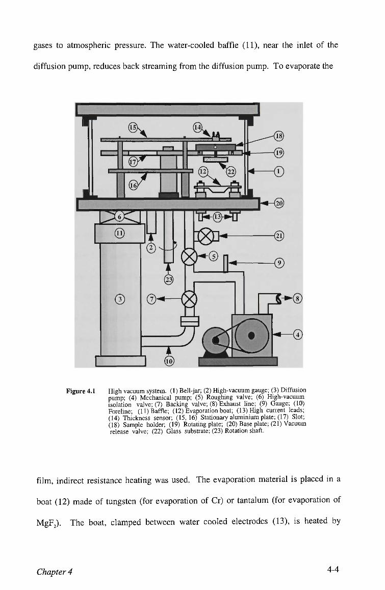
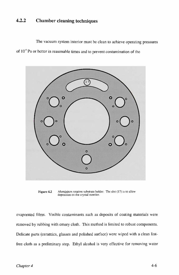
4.2.1 Description of vacuum system 4-3
4.2.2 Chamber cleaning techniques 4-6
4.3 Sample preparation 4-7
4.3.1 Cleaning of substrate surface 4-7
4.3.2 The evaporants 4-9
4.3.3 Actual coating procedure 4-10
4.4 Curvature measurement 4-11
4.5 Calibration of the film thickness monitor 4-13
4.6 Modal resonant vibrational frequency measurements of the substrate/film
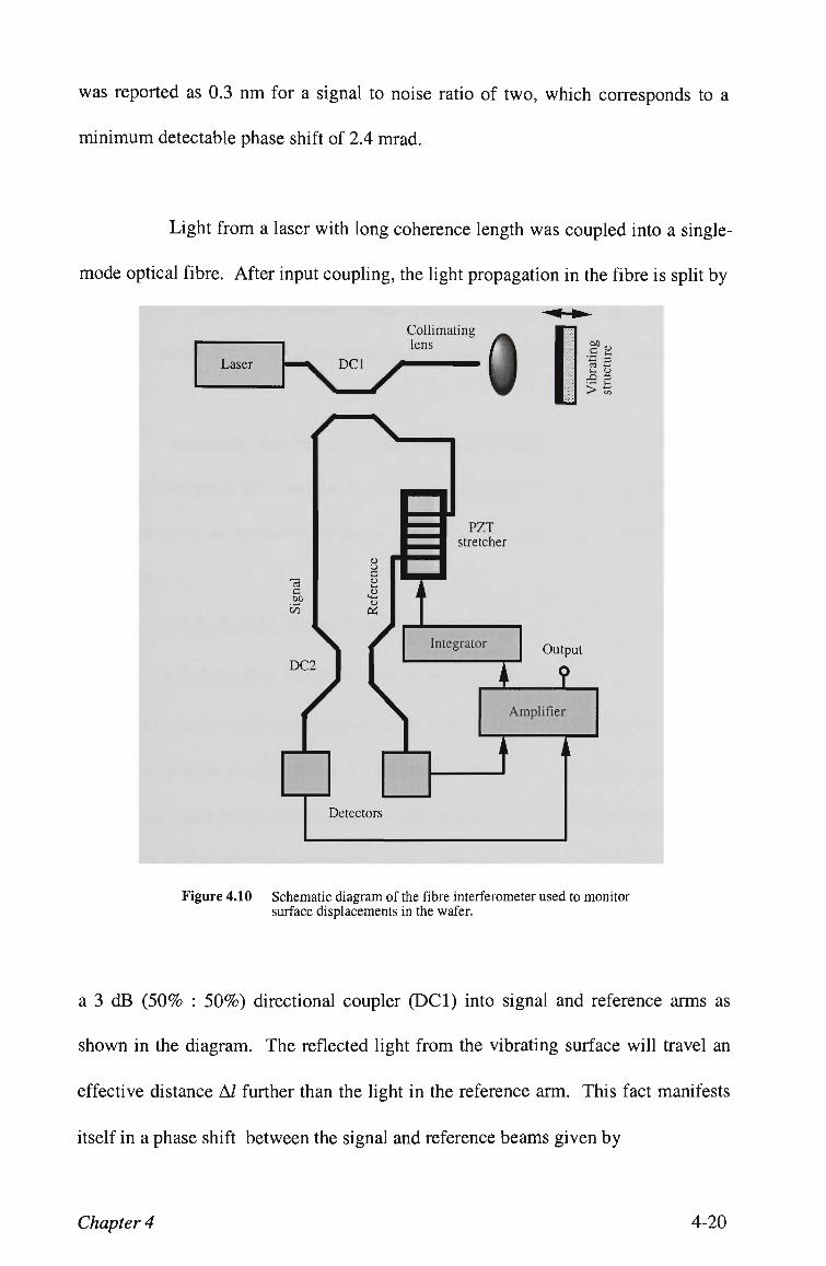
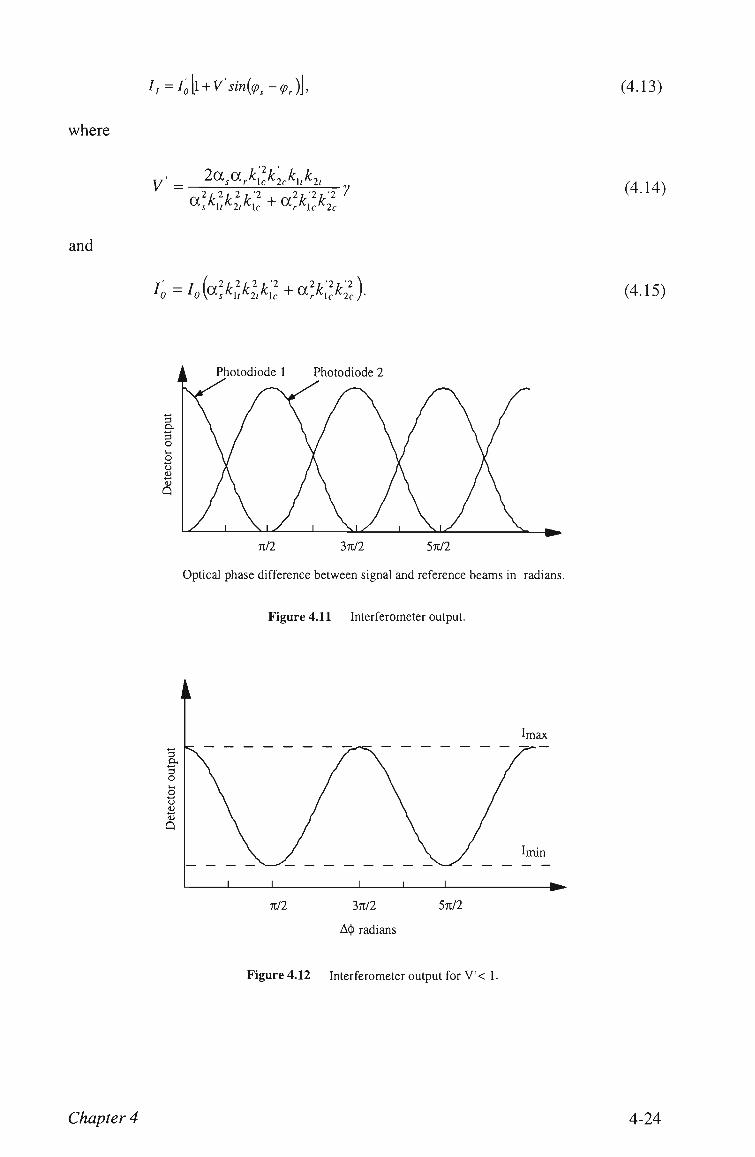
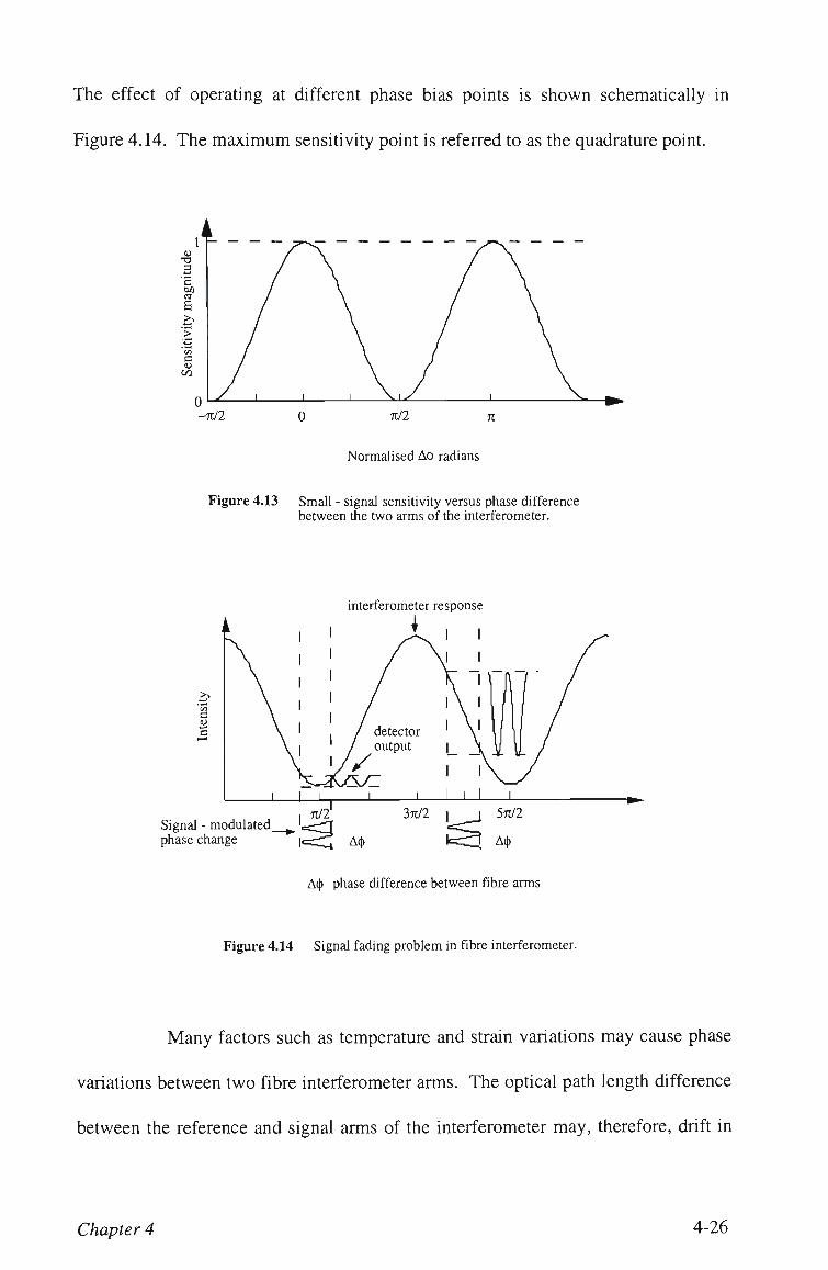
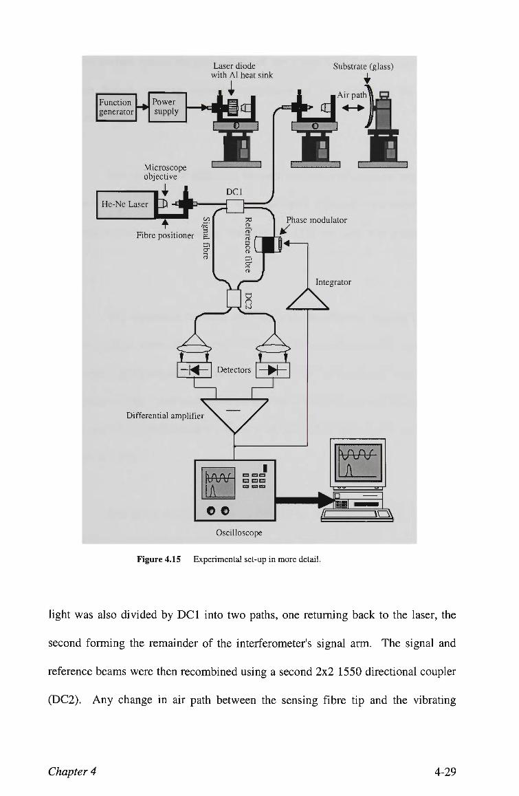
4.6.2 Practical description of the interferometric sensor 4-28
a) Optical layout 4-28
b).Detector and feedback circuitry 4-32
c) Calibration of the interferometer 4-33
4.7 Physical principle of the photothermal excitation mechanism 4-35
4.8 Description of modified vacuum system 4-37
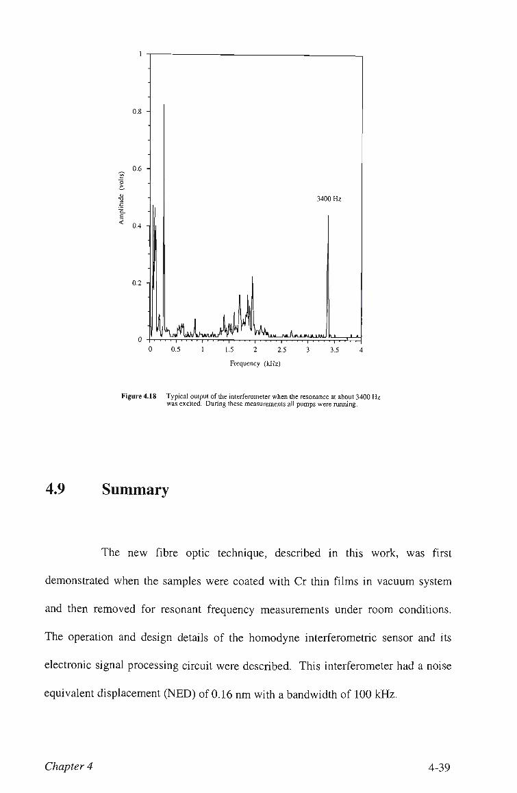
4.9 Summary 4-39
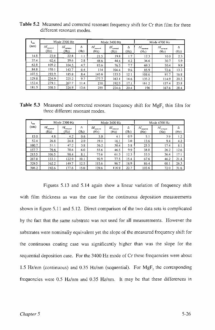
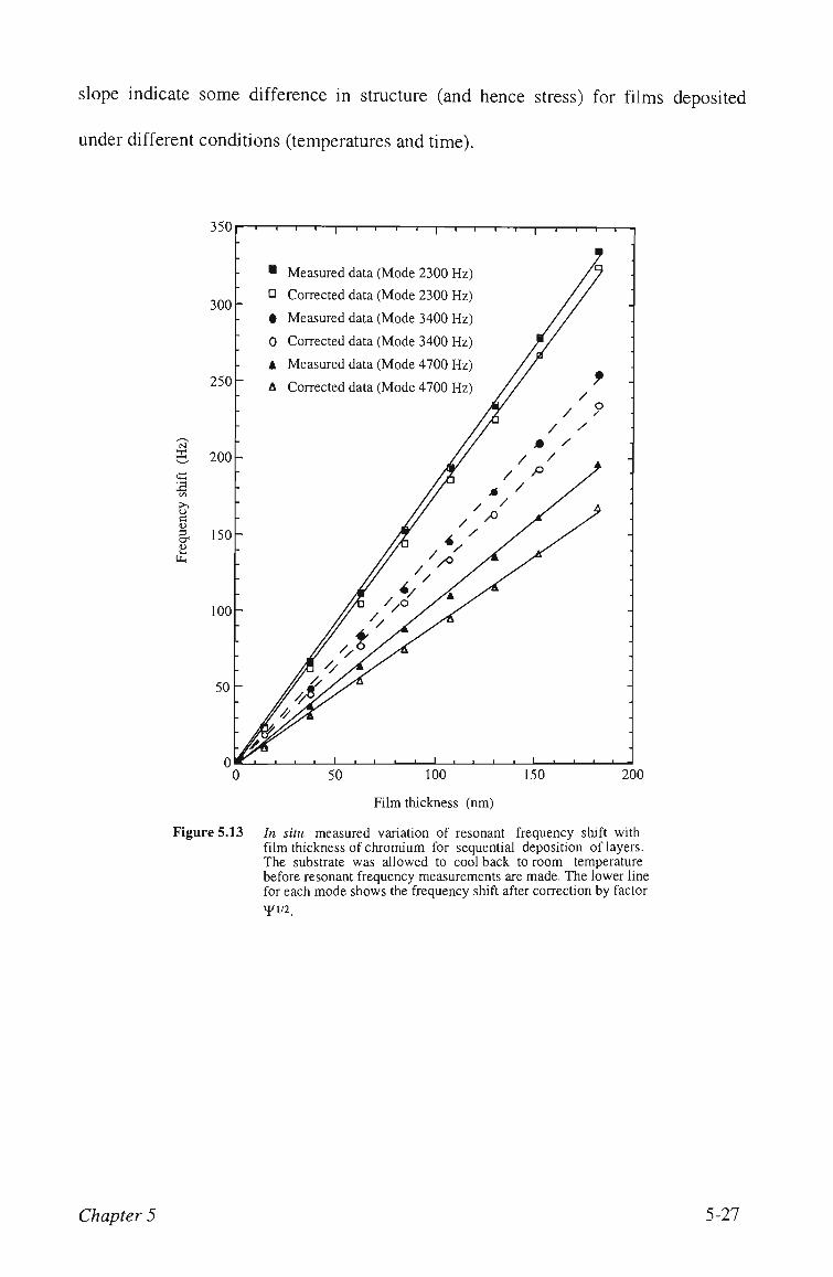
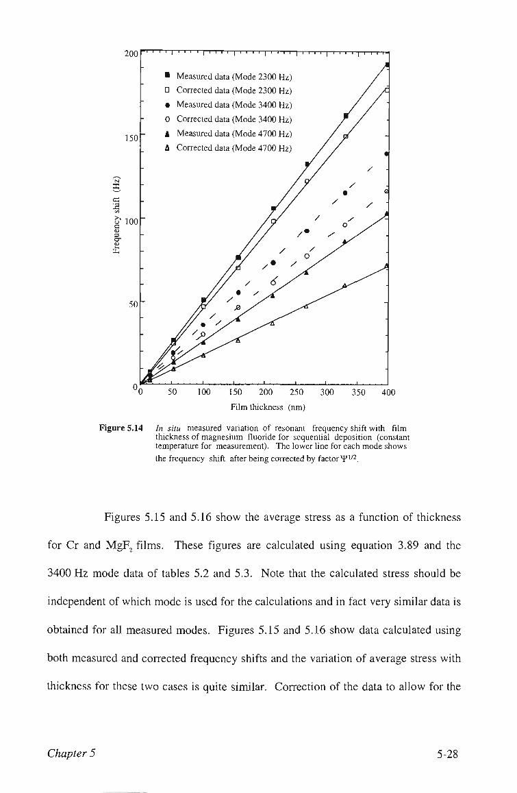
CHAPTER 5. Experimental results and discussion
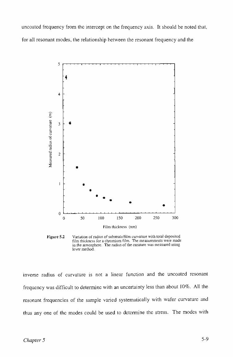
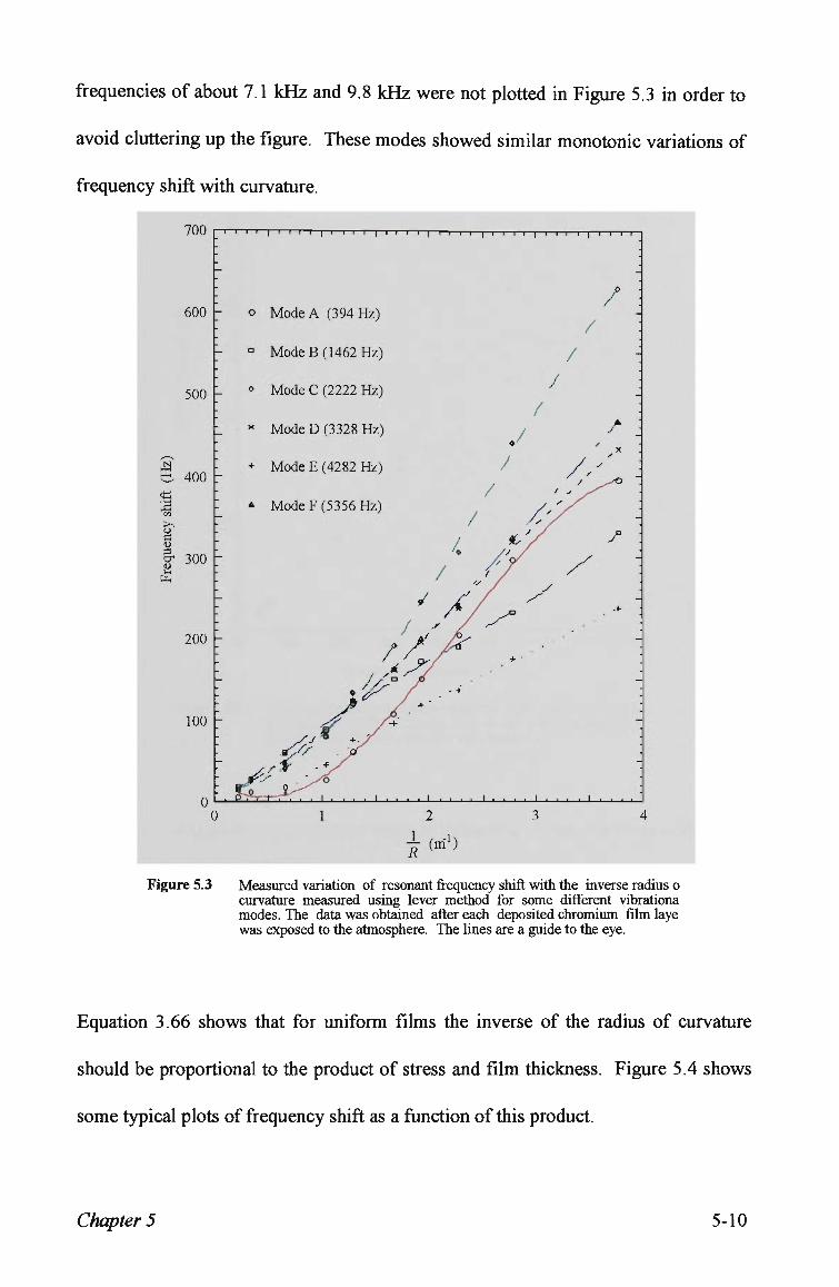
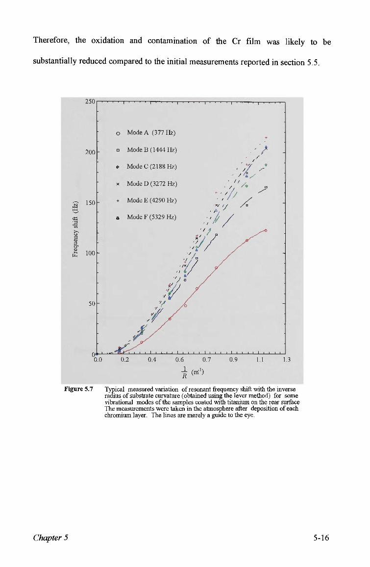
5.1 Introduction 5-1
5.2 Auger Nanoprobe Analysis and depth profiles 5-3
5.3 Initial results with chromium films (measured in air) 5-6
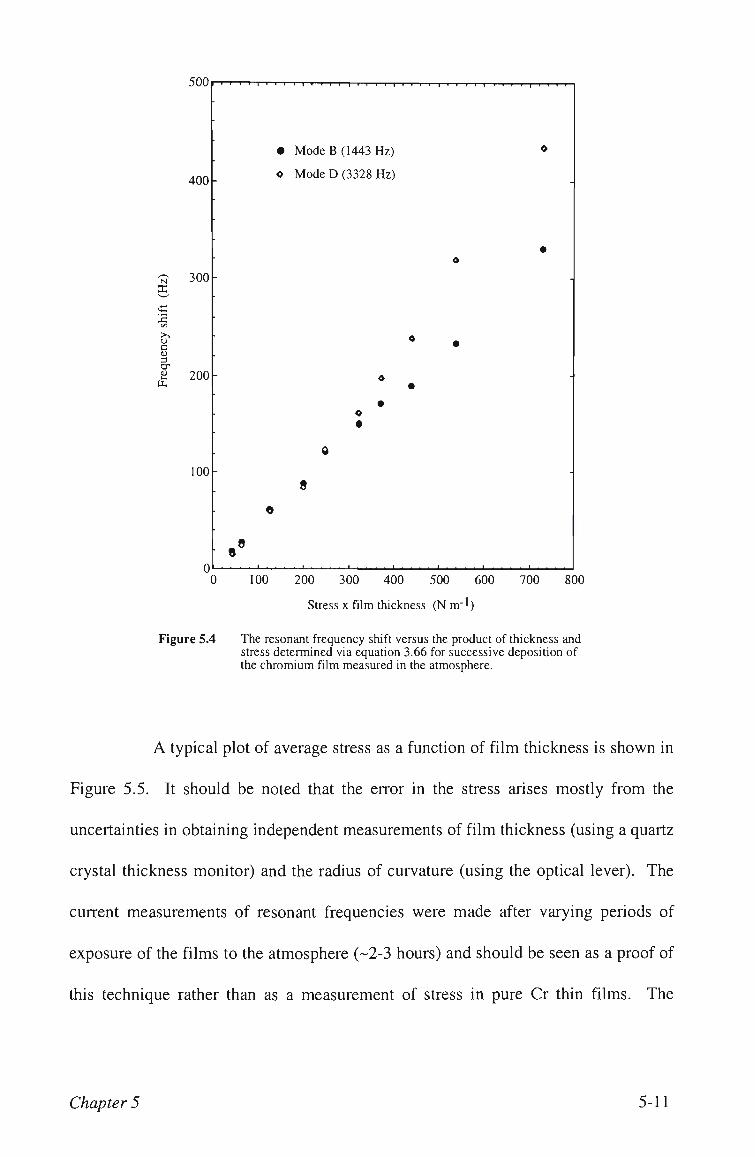
5.4 Measurements of stress when the rear surface of the sample was coated
with a thin titanium film 5-13
5.5 Experimental results for m 5rYM measurements 5-19
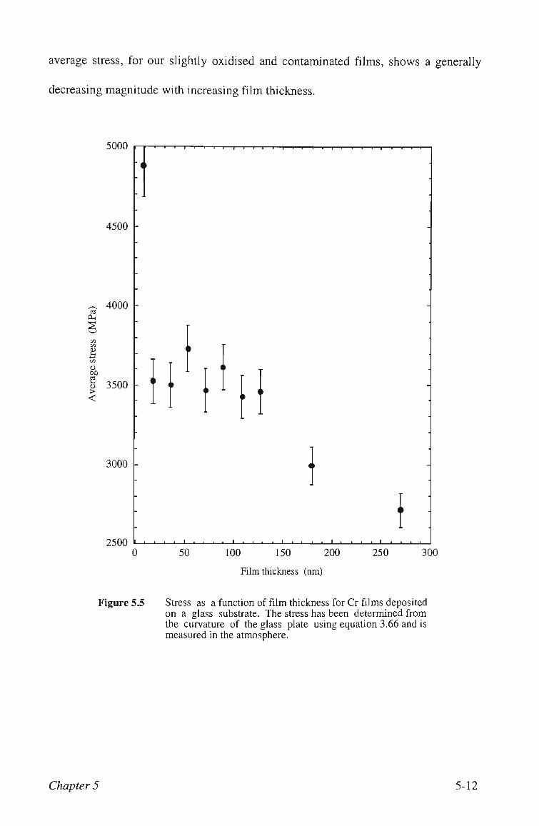
5.6 Summary 5-33
CHAPTER 6. Conclusion
6.1 Conclusion 6-1
6.2 Future work 6-4
REFERENCES
X
APPENDICES
A. 1 Technical data for the glass substrate used in experiments A-2
A.2 Spectrographic analysis of the evaporants according to the manufacturer
specification A-3
A.3 List of figures A-5
A.4 Listoftables A-10
A.5 List of symbols used in this thesis A-12
PUBLICATIONS
X I
Chapter 1
1.1 Introduction
Thin films of many different materials (metals, semiconductors,
inorganic and dielectric materials) are used in an extremely wide range of modem
technological applications. Such applications include dielectric and metallic coating
of components for laser and other optical systems, thin films of semiconductor and
other materials for the production of electronic components and VLSI chips and
decorative and protective coating on a wide range of items. These films frequently
have high intrinsic mechanical stress and the presence of this stress influences the
mechanical, optical, electro-transport, magnetic and superconductive properties of
thin films (Bromley et al, 1983; Leusink et al., 1992; Beck et al., 1998). In extreme
cases, such stress can even result in failure of the thin film by cracking or by
delamination from its substrate. This failure can be immediate or, more seriously,
delayed. Thus there is significant technological interest in measurements that
determine the magnitude of the intemal stress during or at the end of deposition
process. Stress measurements prove to be a highly sensitive tool for the study of
morphology and growth mode of thin films in a non-destmctive manner (Winau et
al, 1992; Malhotra et al, 1997). Such investigations may eventually lead to a better
understanding of the mechanical stress in the film and consequently increase the
reliability of thin film applications (Aberman, 1990; Kylner and Mattsson, 1997).
These investigations are interesting scientifically, since measurements of stress in
thin film should lead to information about which deposition parameters primarily
influence thin film properties. Accurate measurement of the stress in thin films is
rather difficult and a number of methods have been devised (Maissel and Glang,
1970; Vandrieenhuizen et al, 1993; Martin et al, 1998). The present work is
concerned with the development of a new sensitive technique for indirect
measurement of stress variations in thin films which involves the remote
measurement of modal vibrational frequencies when the sample is excited
thermoelastically.
When modulated laser light of appropriate power density illuminates the
sample, the absorbed energy is converted to heat through a non-ablative process
(Opsal and Rosencwaig 1982). Thermoelastic bending (the dmm effect) produced by
transient thermal expansion of the irradiated area causes mechanical vibrations of the
sample (Charpentier and Lepoutre 1982; Crosbie et al, 1986). This thermal bending
process can be produced using low-power modulated laser diode light. When
combined with remote fibre optic vibration sensing, an integrated optical system can
be produced for excitation and measurement of the changes in modal vibration
frequencies of the substrate/film stmcture. Such measurements can be easily
automated and used routinely in industrial laboratories for determination of stress
changes in thin films. This work reports the first use of an all-optical technique based
Chapter 1 1-2
on an optical fibre interferometer for such an application. The optical fibre
interferometer offers considerable advantages in ease of use and robustness compared
to existing methods for stress measurements in thin films. It uses light scattered from
the rear surface of the target stmcture (not necessary highly reflective) and coupled
back into the fibre to produce interference with the reference beam. In such an
arrangement there is no need for bulky and difficult-to-align mirror systems in the
interferometer as in the case in a conventional bulk optic device. However the use of
a fibre interferometer can offer challenging detection problems due to the reduced
signal-to-noise ratios which accompany the reduced light intensities in the interfering
beams. These reduced intensities are due to losses in coupling into and out of the
optical fibres both from the laser source and the beam scattered from the target. In
this work it is shown that with careful design of the fibre interferometer, excellent
signal-to-noise ratios can be obtained using the scattered light from a thin Ti film
applied to the rear surface of the target.
The indirect method for stress determination in thin films, described in
this thesis, relies on measuring the variation of transverse modal vibrational
frequencies of a thin circular substrate on which the thin film is deposited. These
frequencies are a very sensitive function of the curvature of the substrate which is a
function of the stress at the film/substrate boundary. The method was initially
developed using coated substrates which were removed from a vacuum deposition
system in order to perform measurements of vibration frequency and curvature. For
real-time measurements under controlled conditions inside the vacuum system the
previous technique was easily adapted as it only required two optical fibre
Chapter 1 1-3
feedthroughs into the vacuum chamber. A totally remote system for exciting the
vibrational resonances of the substrate/coating and for measuring the resonant
frequency was used. The excitation is via square-wave-modulated low power laser
diode light which is delivered to the substrate in the vacuum chamber via an optical
fibre. The vibration sensing system uses a fibre optic interferometer which requires
only one sensing fibre to be passed through a feedthrough into the coating region.
Using feedback from the interferometer to the laser diode drive electronics, one can
lock the system to track the resonance and obtain a direct readout of stress-related
resonant frequency variations with time as films are deposited or modified by
processes such as exposure to the atmosphere. The technique provides very sensitive
measurements of the substantial changes in resonant frequency with standard errors of
one part in 10 possible with high-Q resonances and constant temperatures.
1.2 Scope of the thesis
This thesis aims to describe the development and evaluation of a new
optical technique for accurate non-contact measurements of residual stress-dependent
modal frequency shifts in thin films coated onto thin glass substrates that could be
easily automated and used routinely in industrial laboratories. This involves:
(i) The design, constmction and characterisation of a laser-diode-based
system for producing thermoelastically-induced mechanical vibrations in
Chapter 1 1-4
substrates and a two beam fibre optic interferometer which can remotely
detect these vibrations.
(ii) Derivation of analytical expressions for the relationship between modal
resonant frequencies and curvature/stress which are appropriate to the
geometry chosen for the experimental measurements.
(iii) Modification and adaptation of a vacuum deposition system to allow it to
be used to test the stress measurement technique.
(iv) Assessment of the effectiveness of the new optically-excited vibrational
resonance technique for stress measurement using metallic and dielectric
films.
1.3 Preview of the thesis
Chapter 2 introduces the concept of stress in thin films and gives an
overview of previous methods for making measurements of residual stress. Since the
stress measurement method developed in this thesis relies on changes in mechanical
resonances of thin plates and shells, this chapter also introduces the essential features
of vibrations in these stmctures.
Chapter 1 1-5
Chapter 3 presents a detailed derivation of the modal resonant
frequencies of a uniform flat circular plate supported at the centre. This derivation is
included as no such treatment covering all modes with these boundary conditions is
to be found in the literature. The modal resonant frequencies predicted by these
expressions are then compared to those deduced from finite element analysis and
measurements made with experimental substrates which have been coated only with
very thin films on front and rear surfaces (just enough to be able to use the excitation
and measurement methods developed in this work). The theoretical results obtained
for a flat plate are then extended to cover the case of a thin spherical shell - the shape
assumed by a substrate which bends under the influence of stress. Chapter 3 also
includes a discussion of the stress and strain relationships as they apply to the
substrate/film stmctures which are studied in this thesis. Equations are derived for
curvature of the substrate as a function of film stress and these equations are
combined with equations for resonant frequency as a function of spherical shell
curvature to obtain expressions which relate both curvature and stress to resonant
frequency. These equations form the basis for analysis of the experimentally-
measured modal frequency shifts in terms of stress and curvature. The final section
of this chapter discusses the effect of the thickness variations and changes of other
physical properties as a result of coating (without any stress) on the resonant
frequencies of the stmcture.
Chapter 4 contains a description of the experimental arrangements and
equipment in sufficient detail for one to properly interpret the experimental results
presented in Chapter 5. Chapter 4 includes details of the vacuum evaporation system
Chapter 1 1-6
and techniques used for sample preparation and coating. It also includes a detailed
description of the optical equipment used for photothermoelastic excitation of the
samples and particularly the interferometer used for resonant frequency
measurement. The discussion of the interferometer includes sufficient theory to
understand its operation as well as techniques used for calibration, locking the
interferometer at the quadrature point and determination of noise limitations on
measurement sensitivity.
Chapter 5 presents results of measurement made using the new technique
with metallic (Cr) and dielectric (MgF2) films. These results clearly demonstrate that
the technique is effective and show that the stress-induced frequency shifts which
arise with these films are substantial. Experimental results are presented for
measurements made in the atmosphere after coatings have been applied in vacuum
and for in-situ measurements made inside the vacuum system including
measurements made while coating is in progress. The effect of temperature changes
during coating is also investigated as is the effect on film stress of exposure of
coatings to the atmosphere.
Chapter 6 is a conclusion chapter which summarises the major
achievements of the work described in this thesis and the advantages of the new
technique for indirect stress determination in thin films. This chapter also make
some brief observations about future extensions of this work and practical
applications.
Chapter 1 1-7
Chapter 2
General overview of the previous work on stress in
thin films
2.1 Introduction
In this chapter a brief description of stmcture and properties of thin films
will be presented and the intrinsic stress in a film will be defined. Then an overview
of previous methods of measuring the stress in thin films will be given. As the
technique for stress measurements in thin films described in this work is based on a
measurement of the modal resonant vibrational frequencies of thin plates and shells, a
brief introduction of dynamics of these stmctures will also be given.
2.2 The nucleation and growth of thin films
The growth of thin films has studied intensively in the past by employing
the entire spectmm of experimental tools ranging from transmission, scanning and
low -energy electron microscopy (Pashley and Stowell, 1966; Venables et al, 1980),
reflection high-, medium- and spot profile analysis low-energy electron diffraction
(Egelhoff and Jacob, 1989; Schneider et al, 1990), Auger electron spectroscopy
(Bauer and Popa, 1984), scanning tunnelling microscopy (Neddermeyer, 1990). In
addition, advanced theoretical film growth simulations were performed with high
speed supercomputer systems (Gilmore and Sprague, 1991; Luedtke and Landman,
1991). It appears, however, that despite these efforts the all processes involved are
not completely understood (Koch, 1994). In this section a short summary of the
present knowledge on nucleation and growth of thin films will be presented.
2.2.1 Thermodynamical consideration
A decisive period of film growth is the nucleation stage at the very beginning
of the film deposition. Thermodynamical theory is applicable only to macroscopic
systems and it may provide useful first insights of the film growth. For the initially
formed nuclei the ratio between the number of surface and/or interface atoms and the
atoms of the bulk is high and their equilibrium shape will depend on the magnitude of
Chapter 2 2-2
the respective free surface and interface energies. The size of equilibrium nuclei
(equilibrium polyhedron) can be calculated from the equation (Koch, 1994):
0, _ 0 -0B _0j^-p _An _kT P
' ~ ' ~ ' ~ 2^~ 2-Q ^~P~ (2.1)
MB MB
where O,. is free surface energy, A|X is chemical potential, k is Boltzmann's constant, T
is substrate temperature, v is the volume of a single film atom, P and Poo are the
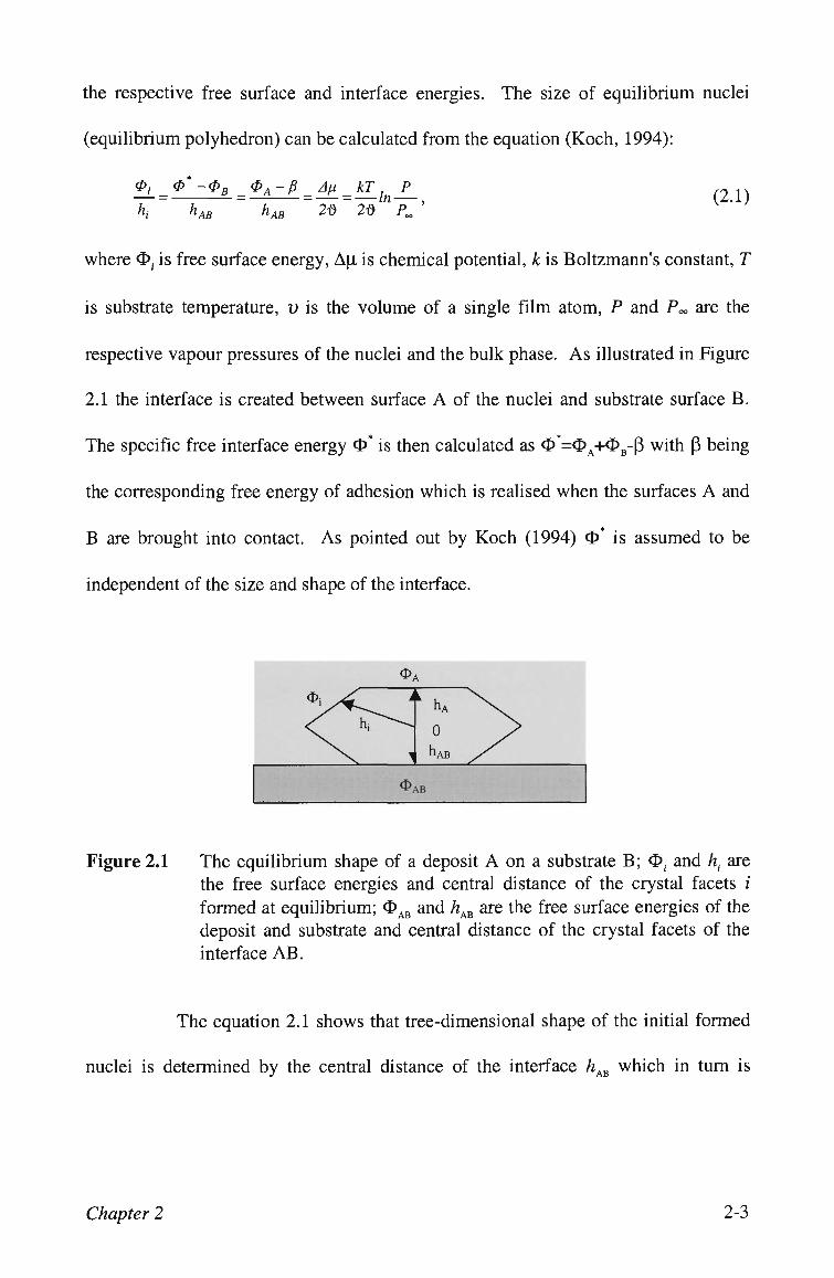
respective vapour pressures of the nuclei and the bulk phase. As illustrated in Figure
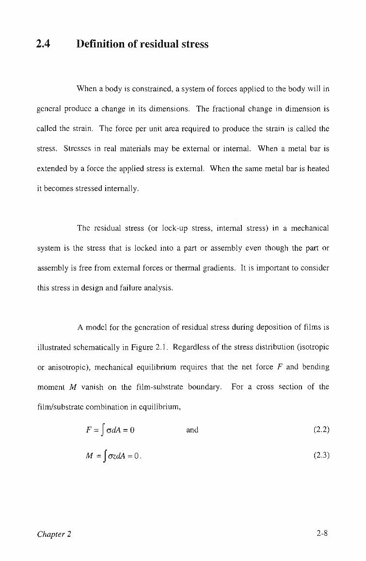
2.1 the interface is created between surface A of the nuclei and substrate surface B.
The specific free interface energy O* is then calculated as 0*=0^-I-OB-P with |3 being
the corresponding free energy of adhesion which is realised when the surfaces A and
B are brought into contact. As pointed out by Koch (1994) O* is assumed to be
independent of the size and shape of the interface.
\
o, . hi
OA
i
^
^ h . \
0 y> hAB y ^
<I>AB
Figure 2.1 The equilibrium shape of a deposit A on a substrate B; O and h. are the free surface energies and central distance of the crystal facets / formed at equilibrium; ^^^ and Ag are the free surface energies of the deposit and substrate and central distance of the crystal facets of the interface AB.
The equation 2.1 shows that tree-dimensional shape of the initial formed
nuclei is determined by the central distance of the interface h^^ which in turn is
Chapter 2 2-3
determined by the relative magnitude of the free energy of adhesion P with respect to
the free energy of the crystal nuclei O^ which forms the top of equilibrium nuclei.
Unfortunately two major obstacles are encountered upon applying
thermodynamical theory to real film/substrate systems:
a) There is a lack of experimental data on the free surface and
interface energies for the numerous possible combinations of thin
film and substrate surfaces so that the predictional value of
thermodynamics for the growth of thin films remains unsatisfied.
b) Usually film growth does not proceed in thermodynamical
equilibrium but it is controlled by kinetic parameters as well.
2.2.2 The role of kinetic parameters on thin film growth
The thermodynamical theory for thin film growth relies on the
assumption of a homogeneous substrate surface which is characterised by an uniform
O' over a large distance. In practice such a surface is hardly ever available. Real
substrate surfaces usually exhibit many different defects such as vacancies, ad-atoms,
stacking faults, dislocations and impurity atoms or molecules which have either
diffused out of the bulk or absorbed from the residual gas in vacuum chamber. As a
consequence of the inhomogeneous O', nuclei of various equilibrium shapes are
formed at the initial stages of film growth. The presence of defects on surfaces may
have substantial influence on the nucleation rate leading to a drastically increased
Chapter 2 2-4
density of nuclei (Shimaoka and Komoriya, 1970). In addition, defects usually affect
strongly diffusion controlled processes of the growing film.
The second parameter that counteracts the influence of defects on the
kinetics of film growth is the substrate temperature which determines the thermal
energy of the diffusing atoms. It was shown (Koch, 1994) that the influence of
certain type of defect is overcome when the substrate temperature is raised. The
influence of deposition parameters on stmcture and properties of thin films is
discussed in the following sections.
2.3 structure and properties of thin films
The properties and stmcture of thin films are strongly affected by its
composition and thickness. The behavior of the film is also affected by the substrate
type, deposition parameters, density of the film and any chemical reactions at the
substrate/film interface.
The substrate type influences the microstmcture of the thin film.
Amorphous substrates such as glasses often contain surface irregularities which can
lead to a non-uniform distribution and orientation of deposited crystallites. For a film
to adhere well it is important that the substrate surface is clean. Good adhesion to
glass substrates is obtained with chemically reactive metals such as chromium or
aluminum (Thun, 1964). Coatings involving atoms of noble metals are usually
Chapter 2 2-5
weakly bonded to a glass surface and hence thick films of such metal are relatively
easily stripped from the substrate.
Deposition parameters also affect the properties of thin films. The three
most important deposition parameters are vacuum pressure, deposition rate and
substrate temperature. The presence of residual gases in the vacuum chamber can
result in stmctural modifications to the film. Gas trapping tends to result in films
with a highly disordered microstmcture. Absorbed gas atoms lead to a decrease of
surface mobility and smaller grain size of the film. The deposition of a thin film with
a 'bulk' stmcture generally requires a vacuum better than 10^ Pa.
Atomic surface mobility is a function of surface temperature
(Neugebauer, 1964), therefore the substrate temperature has a strong influence on
adhesion and the stmcture of thin films. At low substrate temperatures, the resulting
film stmcture depends on the interatomic bond character of the film and substrate
material. With increasing substrate temperature the size of the crystallites increases
and the number of lattice dislocations decreases.
At very low rates of deposition the resulting thin films exhibit roughness
and relatively porous packing (Hoffman, 1966; Tanaka, et al, 1998 ). With higher
rates the film density increases and roughness decreases. The average crystal size
also decreases while the density of lattice faults in the crystallographic film stmcture
increases as there is less time available for atomic rearrangement during deposition.
For example, a 100 nm thick chromium films deposited on a substrate at a
Chapter 2 2-6
temperature of 340°C, had an average grain diameter of about 250 A at deposition
rates below 20 A/sec. With a deposition rate of 40 A/sec the average grain diameter
is about 150 A at the same substrate temperature (Neugebauer, 1959).
Thin films usually exhibit the same crystallographic stmcture as the bulk
material. However, deviations from the properties of the bulk materials can be
caused by small film thickness, large surface to volume ratios and high stmctural
disorder. Small film thickness affects the electric, magnetic and mechanical
properties. The high surface-to-volume ratio of a film increases the influence of gas
adsorption, diffusion and chemical reactions at the film surface or film-substrate
interface. High stmctural disorder of materials (for instance amorphous stmcture)
can lead to mechanical, electrical and magnetic properties which differ from those in
bulk crystals by orders of magnitude (Hoffman, 1966; Vinci and Vlassak, 1996).
Annealing has often been used to improve the stmcture and properties of thin films
(Sinha et al, 1978; Flinn, 1989; Scardi, etal, 1994).
Increasing interest in fundamental solid state physics and many areas of
technology including the semiconductor, optics, decorative and protective coating
industries require better understanding of the influence of the deposition parameters
on one hand and on the correlation between stmcture and physical film properties on
the other.
Chapter 2 2-7
2.4 Definition of residual stress
When a body is constrained, a system of forces applied to the body will in
general produce a change in its dimensions. The fractional change in dimension is
called the strain. The force per unit area required to produce the strain is called the
stress. Stresses in real materials may be external or intemal. When a metal bar is
extended by a force the applied stress is external. When the same metal bar is heated
it becomes stressed intemally.
The residual stress (or lock-up stress, intemal stress) in a mechanical
system is the stress that is locked into a part or assembly even though the part or
assembly is free from external forces or thermal gradients. It is important to consider
this stress in design and failure analysis.
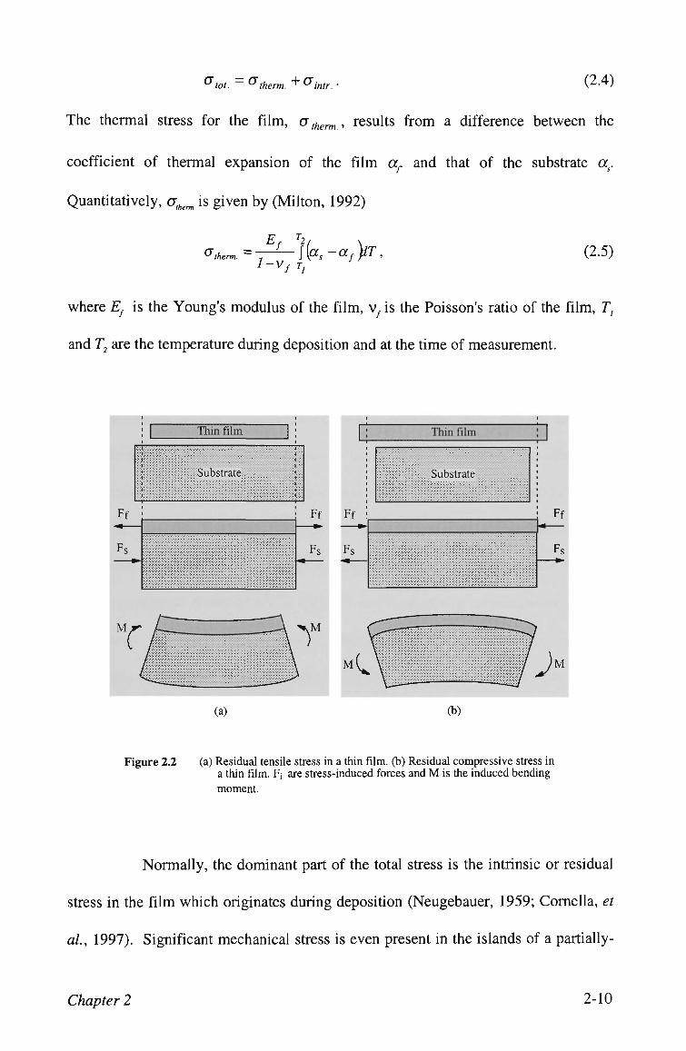
A model for the generation of residual stress during deposition of films is
illustrated schematically in Figure 2.1. Regardless of the stress distribution (isotropic
or anisotropic), mechanical equilibrium requires that the net force F and bending
moment M vanish on the film-substrate boundary. For a cross section of the
film/substrate combination in equilibrium,
F = Jad!A = 0 and (2.2)
M=^GzdA^Q. (2.3)
Chapter 2 2-8
Here o is residual stress, dA is the element of cross-sectional area and z is the distance
from the chosen neutral axis as shown in Figure 3.10(c). These basic equations will
be used in deriving the formula for stress in thin films (section 3.8).
In the first type of behaviour shown schematically in Figure 2.1(a), the
growing film initially shrinks relative to a substrate. Surface tension forces and misfit
of atomic spacing could be the reasons why this might happen. However, both the
film and substrate must have the same length and the film stretches while the
substrate contracts. Therefore, the tensile forces developed in the film are balanced
by the compressive forces in the substrate. The film/substrate system is still not in
mechanical equiUbrium because of the uncompensated end moments. If the substrate
is not rigidly held it will elastically deform to counteract the unbalanced moments.
Thus, thin films with tensile residual stresses bend the substrate concavely. In an
entirely similar fashion a film which develops residual compressive stresses will
contract relative to substrates, as shown in Figure 2.1(b). Therefore, residual
compressive film stresses bend the substrate convexly. By convention, the radius of
curvature, R, of the substrate/film stmcture is positive for concave curvature (tensile
stress) and negative for convex curvature (compressive stress).
Thermal effects provide significant contributions to film stress (Flinn,
1989). Films prepared at elevated temperatures and then cooled to room temperature
or films which are thermally cycled, will be thermally stressed due to differential
thermal effects. Therefore, the total mechanical stress o-f , has two components, the
thermal stress a^^^^ and the intrinsic stress cr , . Hence,
Chapter 2 2-9
^tot. ^therm. " ^intr. (2.4)
The thermal stress for the film, <7 therm. ^ results from a difference between the
coefficient of thermal expansion of the film a^ and that of the substrate a^.
Quantitatively, G^^^^^ is given by (Milton, 1992)
(^ therm. = ' 1 i « . 'CCfPT, 1-Vf Tj
(2.5)
where E^ is the Young's modulus of the film, v is the Poisson's ratio of the film, T^
and T^ are the temperature during deposition and at the time of measurement.
Figure 2.2 (a) Residual tensile stress in a thin film, (b) Residual compressive stress in a thin film. F; are stress-induced forces and M is the induced bending moment.
Normally, the dominant part of the total stress is the intrinsic or residual
stress in the film which originates during deposition (Neugebauer, 1959; Cornelia, et
al, 1997). Significant mechanical stress is even present in the islands of a partially-
Chapter 2 2-10
formed film produced during the initial stages of deposition on the substrate. During
the network stage of film growth, bridges between the islands are observed and
finally a continuous film is formed. Often the maximum stress is reached when the
first layer of the film is formed.
The residual stress strongly depends on lattice defects produced during
the condensation process. Even in single-crystal films, dislocation concentrations are
of the order of 10'° to lO'Vcm^ (Neugebauer et al, 1959). Such concentration of
dislocations in a metal would result in a heavily deformed stmcture (Kittel, 1976). At
film thicknesses of 100 nm and below, these dislocations extend through the entire
film thickness. High concentrations of lattice defects influence the other film
properties. Due to scattering of the charge carriers at the lattice defects, higher
electrical resistance has been observed in metal films compared to bulk material
(Horikoshi and Tamura, 1963; Vandamme and Vankemenade, 1997). There is also a
strong correlation between lattice disorder and magnetic or superconducting film
properties. The stress caused by lattice imperfections can be relieved by annealing
after film deposition or, more effectively, by heating of the substrate during
deposition. Since higher substrate temperatures can increase the thermal stress the
optimum deposition temperature must be found by experiment (Neugebauer et al,
1959; Koch, 1994; Honda, et al, 1997).
Intrinsic stress can also be generated by trapped gas and impurity atoms.
There has been no comprehensive study reported in the literature on the influence of
residual gas incorporation during deposition on thin film stress. The approach has
Chapter 2 2-11
been generally to improve the vacuum until the film is pure enough to show no
appreciable degradation. Nevertheless the effects of gas contamination can be
significant. Oxides or other chemically bonded surface layers can contribute to the
residual stress. Significant effects on the intrinsic stress were observed even at low
oxygen partial pressure (10' Pa) in metallic thin films (Winau, 1992). In another
study, it was observed that small amount of oxygen incorporated in thin aluminium
film can change the sign of the stress (Thumer and Aberman, 1990).
Water absorbed by dielectric optical thin films causes (in a multilayer
thin film stmcture) the central wavelength of narrow band optical filters to shift to a
longer wavelength (Macleod and Richmond, 1976). The stress reduction in a thin
film of MgF^ due to the water vapour absorption, when the film is exposed to the
atmosphere, is between 40% and 100% (Pulker, 1982; Martin, etal, 1998).
Thin film coatings are amongst the most problematic and easily damaged
components in any high power laser system due to the residual optical power
absorbed in the film. They can be considered the prime constraint to improved
system performance. The interaction process between laser beam and thin film is
very complex but often the laser beam energy is absorbed by defects in thin films
(Glass and Guenter, 1978). This produces breakdown heating in the film and when
the temperature rise exceeds some critical value, the induced thermal stress can cause
failure of the film. It is well established that the film's intemal stress is one of the
parameters that affect not only laser induced pulsed damage but also the durability of
thin films (Glass and Guenter, 1978). Coatings with minimum possible intemal
Chapter 2 2-12
stress are needed for high power laser applications and this is one of the motivations
for the development of the new stress measurement technique described in this thesis.
There is significant interest in measurement techniques which allow
accurate measurement of intemal stress at the end of deposition process and
variations of the stress which are produced under varied deposition conditions.
Accurate measurement of the stress in thin films is rather difficult and a number of
methods have been devised and described in the literature. These methods, and
previous work on stress measurement in thin films, are summarised in the next
section.
2.5 Experimental methods for measuring the stress in
thin films
A wide variety of techniques have been employed to measure intemal
stresses. Good critical accounts of them have been given by Campbell (1963) and
Hoffman (1966). Excellent reviews of the methods for thin film stress measurement
has also been given by Maissel and Glang (1970) and Vinci and Vlassak. (1996).
If the substrate is flexible and the film adheres strongly to the substrate,
intemal stresses will produce a change in shape in the film/substrate system which
can then be measured and used to determine the intrinsic stresses developed in the
Chapter 2 2-13
film during deposition. Two substrate/film configurations have been primarily used
to indirectly estimate, in situ, the stresses in thin films:
(a) Bending plate or membrane methods.
(b) Bending beam methods.
Other methods (e.g. electron or X-ray diffraction) may also be used but these are
generally not suitable for in situ measurement.
2.5.1 Circular membranes and bending plate methods
Circular membranes of thin film material have been used to determine the
residual stress by measuring the deformation (bulge height) versus pressure (Bromley,
et al, 1983). A clean 5.08 cm diameter silicon wafer was coated with l[im of silicon
nitride. A circular window pattern was opened on the wafer backside by conventional
photolithography and gas plasma etching. The silicon was than etched away using
appropriate chemical solution. The stress will bow the film membrane without
pressure applied and the deflection 6 can be related to the residual stress by
CT^ = . / ^ X , ( 2 . 6 ) 5 ( 7 - v , ) r '
where £^is the Young's modulus of the film, v^is Poisson's ratio and r is the radius of
the hole. A known pressure difference was applied on both sides of a membrane.
The deflection of the center of the membrane is measured by counting the number of
fringes of the reflected interference pattern between a flat mirror and the center of the
membrane as a function of pressure. Assuming that the deflection of the membrane is
Chapter 2 2-14
small compared to its radius, the equation connecting pressure and membrane
deflection was found to be
4t.5 2E.5^ G, +• f nf-i _^,,\^2 3{l-v)r
(2.7)
where t^is the film thickness. The resolution of stress measurement using this method
was found to be approximately 10 Pa.
A vibrational technique for stress measurement in films has been
developed by Maden et al (1994). The technique is based on the theory of
membranes. A 76 im thick copper sheet was mounted on a square glass plate. A
polyamic acid was spin-coated onto the copper substrate. Then, the plate was cured
for one hour in a nitrogen atmosphere. After curing, the polyamide film was 10±0.5
nm thick. The sample was removed from the glass plate and the back side of the
copper was coated with positive photoresist. A circular mask was used to expose the
photoresist. The resist was then developed and the exposed copper was etched away
in an appropriate chemical solution. After etching, the sample was rinsed with water
and dried.
The natural transverse vibrational frequencies, to , for a circular
membrane of radius a, for geometry described above, are given by
^,2 r/, ^ 2 mn ^ (2.8)
P V a J
where u, is the m-th root of / (x), the n-th order Bessel function of the first kind, a is r mn n^ ^'
stress and p is the density of the film. This technique does not require a knowledge of
Chapter 2 2-15
the elastic constants of the film and offers a direct stress measurement. The main
drawback of this technique is that buckling can occur in the film. The membranes are
also highly sensitive to air currents and audio noise. The resonant frequencies were
excited by a mechanical shaker which can cause some difficulties in interpretation of
data when the membrane's natural frequencies are close to the natural frequencies of
clamping stmcture.
A second type of 2D substrate configuration frequently employed for
stress measurements is the circular plate (Finegan and Hoffman, 1959; Kinbara,
1961; Glang, et al, 1965). The change in the radius of Newton's rings formed
between the substrate and an optical flat can be used to measure the deflection of the
plate produced by stress. This method also offers the possibility of observing stress
anisotropy. This is not an in situ method and hence is not suitable for stress
measurements during film deposition. A sensor head for in situ measurement of
stress anisotropy in thin films has been developed by Homauer, et al, 1990. The
method employs an array of capacitor probes and the shape of the deforming plate
was determined by monitoring the electrical signals and processing the data by
computer.
An optically levered laser technique schematically shown in Figure 4.6, to
measure wafer curvature has also been used (Sinha et al, 1978;Rosakis, et al, 1998;
Windischmann and Gray, 1995) for residual stress measurements. This technique has
so far provided one of the best combinations of accuracy, convenience and speed for
most applications (Flinn et al, 1989). A laser beam is reflected from the coated
Chapter 2 2-16
substrate onto a screen at a known distance from the substrate (section 4.4). From the
position of the reflected spot on the screen, the radius, R, of the curved film/substrate
composite is calculated using
Ax R = 2L . (2.9)
Ax + Ad
Here Ax and At/are the distances of the laser beam and its reflection from the
symmetry axis perpendicular to the curved film/substrate stmcture and L is the
distance of the measuring screen from the curved stmcture. The film stress can be
calculated using Et^
Gftf= '-^ . (2.10) ^^ 6R(l-vJ
Here E^ and v are the Young's modulus and Poisson's ratio for the glass substrate, t^
is the thickness of the substrate and tj, ( « t) is the film thickness. Equation 2.10
assumes that the substrate is flat before coating. If this is not the case and the initial
radius of curvature of the substrate is Kg before coating, then equation (2.10) becomes
(Sahu et a/., 1990; Leusink et al,1992)
Est; Gftf =
^^ 6(1-V)[R Rn (2.11)
5 / V •"• ^^0 J
It should be noted that the use of laser deflection measurements together with
equations 2.10 and 2.11 actually gives the product of stress and film thickness.
Independent knowledge of the film thickness (via an additional thickness
measurement) is necessary for separate determination of stress.
For measurement of stress changes in a coated sample during thermal
cycling, a technique for curvature measurement using a scanning laser method was
Chapter 2 2-17
developed (Flinn et al, 1987). A laser beam is reflected from the surface of the
substrate and the displacement of the beam is determined using a position sensitive
detector. The wafer was scanned by an oscillating mirror.
Heterodyne interferometry has also been used to measure the curvature of
a uniformly coated 1 \ivi\ thick silicon nitride film on a 200 im thick silicon substrate
(Nie, 1980). A gas laser having two orthogonally-polarised outputs which differ in
frequency by 1.8 MHz was used for this measurement. These beams were separated
in an interferometer and recombined at a detector in such a way that interference was
produced after one of the beams was reflected from the coated substrate and the other
from a reference retro-reflector. The phase of the output signal of the detector is
directly proportional to the bending displacement of the coated substrate at the point
where the reflection occurred. The curvature of the substrate was calculated by
means of a least-squares curve-fitting program which fitted a circular arc to the
measured deflection as the substrate/film combination was scanned across the
interferometer beam. This method has limited usefulness for stress measurements as
it requires a series of measurements for one sample and is not carried out in situ.
2.5.2 Bending - beam methods
In these methods a thin strip of glass or other substrate is rigidly clamped
at one end in a fixed mount to form a cantilever onto which the film is deposited.
Chapter 2 2-18
The deflection of the free end, as the strip becomes bent, is then measured by some
means. The principal methods used for deflection measurement are:
(1) Direct optical observation of the free end with a microscope
(Murbach and Wilman, 1953; Novice, 1962).
(2) Measurement of the electrical capacity formed between the flexible
strip and the fixed conducting plate held parallel and close to it
(Blackburn and Campbell, 1961).
(3) Electromechanical measurement of the deflection using a stylus
pick-up touching the free end of the cantilever (Campbell, 1963).
(4) Counting interference fringes formed in a laser interferometer
which uses one beam reflected from the free end of the cantiliver
(Ennos, 1966; Cardinale, et al, 1996).
The deflection of one side of the substrate is proportional to the bending
moment exerted on the substrate by the film. The bending moment is also
proportional to CT/tf, where / is the film thickness and CTf is the average stress in
the film. By substituting the radius of the curvature of the beam, R-P/ (2<5), in
equation 2.10, the film stress can be calculated using
a / V = 7 - ^ ^ 6 . (2.12) ^ ^ ( l - v j 3 / 2
In this equation / is the length of the cantilever beam, 8 is the beam deflection at the
end, t^ is the beam (substrate) thickness and E^ and v are the Young's modulus and
Poisson's ratio of the beam, respectively. The sense of the deflection is a direct
indication of the kind of stress in the film. For a film deposited on the underside of
Chapter 2 2-19
the substrate, an upward deflection indicates a compressive stress in the film and
tensile stress causes a downward deflection.
2.5.3 Electron-diffraction and X-ray method
Methods based on X-ray and electron diffraction have been used to
measure changes in lattice spacing and hence stresses in films. Halliday et al. (1954)
has published a detailed treatment of stress determination by electron diffraction.
The X-ray technique is preferable to electron diffraction because of the higher
sensitivity which exists for the larger Bragg angles available and a minimum strain of
10' has been achieved (Vreeland et al, 1989; Uchida, et al, 1999). The stress
(assumed isotropic) in the film plane is computed from the fractional change in the
lattice constant given by the relation
G , = ^ ' - ^ , (2.13) 1-^s «0
where ao and a are the lattice constant of the unstressed bulk material and the film,
respectively.
2.5.4 Other techniques
Any physical property of the film affected by stress can in principle be
used to measure the stress or sense changes in stress. Stress in ferromagnetic films
will produce an anisotropy in magnetisation as a result of magneto-elastic coupling.
Chapter 2 2-20
Since the ferromagnetic resonance frequency depends on the anisotropy as well as the
magnetisation, a shift in the resonance peak will occur (MacDonald, 1957).
A single mode optical fibre sensor has been used for the measurement of
stress in optical coatings (Shouyao and Jiu-Lin, 1992). Two fibres were attached
around a stress sensitive strip. Bending of the strip due to induced stress in its
deposited film strains the fibre causing a phase change in light passing through. By
counting the fringes the stress was deduced. The drawback with this technique is that
the film is also deposited on the fibre and the stress in the film causes the strain in the
fibre as well.
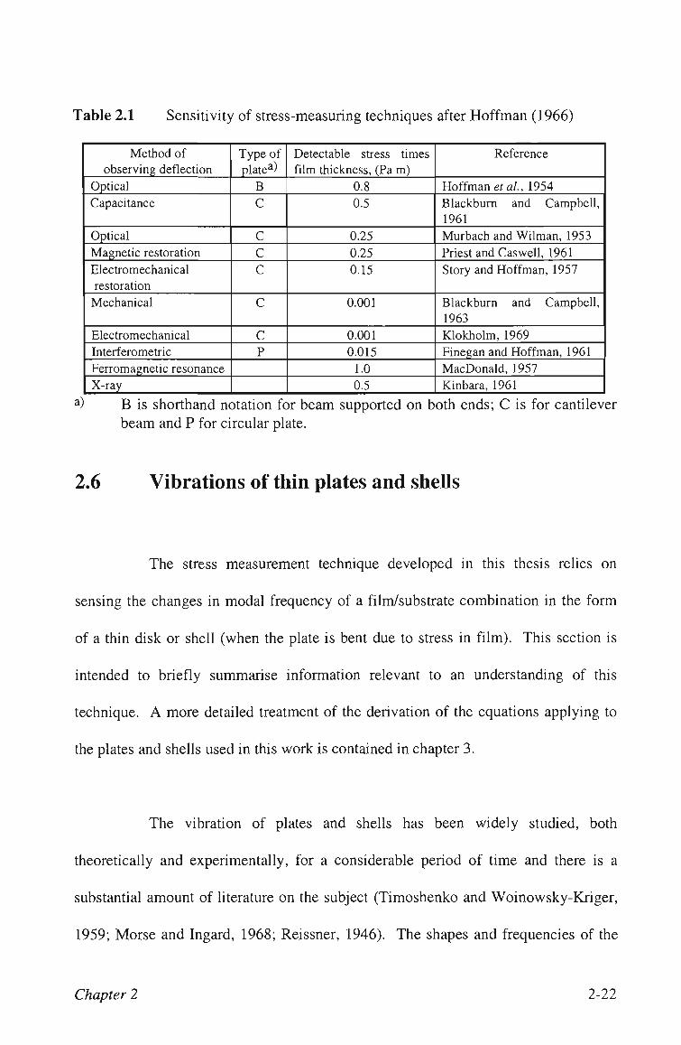
Table 2.1 summarises the measured performance obtained with a range of
techniques for measuring the deflection of the cantilever beam or plate caused by
developed stress in the deposited film. While this table is relatively old,
improvements have mostly been made in the quality of the films (due to better
vacuums) rather than the sensitivity of the techniques for stress measurement. Hence,
the data in Table 2-1 still gives a reasonable picture of the situation with regard to the
sensitivity of the techniques. Data is also included in the table for some non-
deflection methods for comparison purposes. For thicker films these methods are
sufficiently sensitive but, during initial film growth, where stress is small, the more
sensitive interferometric methods are needed. With all techniques involving bending
or deformation of the substrate, the effect of the stress caused by the film will be
larger if the thickness of the substrate is decreased. Hence it is generally possible to
improve sensitivity by appropriate choice of substrate.
Chapter 2 2-21
Table 2.1 Sensitivity of stress-measuring techniques after Hoffman (1966)
Method of observing deflection
Optical Capacitance
Optical Magnetic restoration Electromechanical restoration Mechanical
This equation determines the allowed values of the frequency, because b = ka and k
depends on frequency. For each value of m there will be an infinite number of solutions
of equation (3.37). Labelling the allowed values of the frequency f^ where m is the
number of diametrical nodal lines and n is the number of circular nodes the equations
(3.5) and (3.37) can be written as
12;rVi^(^-v^) Eh'
k' = -^^^ -, (3.38) mn 177^2 ' ^ •'
and
LK)-RK) = 0, (3.39)
where b„„ = k^ a. mn mn
Nine values for b^^ have been calculated by interpolation of equation (3.37) using
Mathematica software:
b,, = 1.92853 b,, = 4.55962 b„, = 7.780656
b,, = 2.49691 b,, = 5.817204 b„ = 9.021673
b,, = 3.75798 b,, = 7.239655 b,, = 10.4927049.
It should be mentioned that the equation 3.39 is sensitive to the number of decimal
places. The allowed values of the frequency are therefore
Chapter 3 3-9
f = J mn
h •{bmn) iTia'^"'"^ pp(l-v') '
(3.40)
and the fundamental frequency is
^"'="^4J -Another way of writing these results is
fn= 1-677^
f2t = 3.799/,
fo2= 5.593/,
/ . = 9.103/,
/ , = 14.099/,
4 = 16.225/,
/ , = 21.894/,
/ , = 29.617/,.
As can be seen, the non fundamental frequencies of vibration are not integral multiples
of/,, hence the allowed frequencies do not form a harmonic series. If r is very small
(the region around clamping point) the terms involving Inikr) in equations (3.16) and
(3.17) are dominant, then we can write equation (3.19) as
y] = B[zJkr)-Hjkr)]sm{m).
By substituting the equations 3.16 and 3.17 the equation 3.41 becomes
T] = B[jjkr) - ljkr)]ln{ki)sm{(0t),
(3.41)
(3.42)
or
t] = -2B ^ k V k'r'
2242^2 +... ln{kr)sm{o)t). (3.43)
Thus when r is small we can write
r]=-—Bk'r' In kr sin{cot) (3.44)
Chapter 3 3-10
By combining equations 3.39 and 3.3 the approximate value of the shear force when r is
small is given by
F = 1 EBk%' d
3 ( l - v ' ) dr \_d_
r dr
f d(r'lnkrf df~
(3.45)
F = -4 EBk'h' 1
3 1-n' r (3.46)
Equation 3.46 suggests an infinite shearing force at the centre of the plate.
Thus the conditions we have assumed in this derivation (specifically that the plate is
fixed at a point in the centre) cannot exist in practice. In reality the plate is held fixed
over a finite circular region. The results presented here should apply with fair accuracy
when the support is small compared to the radius of a plate. The dynamic analysis of a
flat glass plate, using Finite Element Modelling (FEM), has shown that a 7% increase of
the radius of the metal support rods will cause the frequency changes of 0.01 Hz. In
addition, the radius of circular glass plates used in experiments was 28 times larger than
the radius of the metal support rods, so equation 3.40 can be applied with confidence.
Chapter 3 3-11
3.4 3D plots of solution for circular plate clamped at the
center
Figures 3.1 to 3.3 shows instantaneous three-dimensional plots of the
vibrational amplitudes for nine of the vibrational modes of the flat plate. These modal
shapes are obtained by plotting equation 3.42.
3.5 Calculated and measured resonant mechanical
vibration of substrate used for stress measurement in
thin Alms
The substrates used to measure the stress in thin films were thin glass plates as
described in section 4.3.1. Substitution of appropriate constants for the glass plate [E^ =
7.2x10'° Pa, V = 0.25, (Malecki, 1969), p = 2.51x10' kg/m' (as shown in Appendix 1), a
= 21x10"' m and 2h = 110 im] in equation (3.40) gives
L„=63.55x(bl). (3.47)
The calculated values for natural resonant frequencies of the first nine vibration modes
are given in Table 3.1.
Chapter 3 3-12
o; = 1.92853 /o; = 236.3 Hz
bo2-4.55962 /02 =1320.7 Hz
bo3 ^ 7.780656 f^ = 3845.7 Hz
Figure 3.1 Representation of the first 3 natural modes of vibration of a circular plate clamped at the center. The frequencies of vibration do not form a harmonic series.
Chapter 3 3-13
b „ = 2.49691 / „ =396.0 Hz
b,2 = 5.817204 / i2 =2149.7 Hz
b,3 = 9.021673 / , 3 =5170.3 Hz
Figure 3.2 Representation of the 4*"", 5* and 6^ natural modes of vibration of a circular plate clamped at the center.
Chapter 3 3-14
b2, =3.75798 / 2 , =897.1 Hz
^22-7.239655 /22 = 3329.5 Hz
b23 = 10.4927049 /23 = 6993.9 Hz
Figure 3.3 Representation of the 7*, 8* and 9* natural modes of vibration of a circular plate clamped at the center.
Chapter 3 3-15
Table 3.1 Calculated value for natural resonant frequency for flat circular glass plate clamped in the center.
/ = 236.3 Hz •'oi
f = 1320.7 Hz •^02
f =3845.7 Hz
f = 396.0 Hz
f =2149.7 Hz •'12
f =5170.3 Hz
f = 897.1 Hz •'21
f =3329.5 Hz •'22
f =6993.9 Hz •'23
To preserve the flatness of the plate during optical measurements to check
these frequencies, a 10 nm thick chromium film was deposited on both side of glass
sample as shown in figure 3.4. The flatness of the sample was measured using an optical
lever technique as describe in section 4.5.1. These measurements confirmed that there
was negligible change in the flatness produced by gluing the metal support rod in the
centre of the sample. The sample was than placed in the vacuum system and the
frequency measurements were obtained in the air and under a vacuum of 10' Pa. The
measured values are presented in Table 3.2. The removal of the damping produced by
the air typically increases the resonance frequency of the sample, for modes with
resonant frequencies above 2 kHz by less than 1%. While these frequency changes are
Metal rod
1 glass
Chromium film
Chromium film
Figure 3.4 The sample used to measure the frequency of flat plate.
Chapter 3 3-16
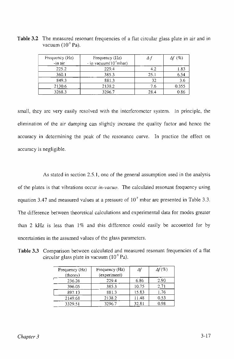
Table 3.2 The measured resonant frequencies of a flat circular glass plate in air and in vacuum (10"' Pa).
Frequency (Hz) -in air
225.2 360.1 849.3
2130.6 3268.3
Frequency (Hz) - in vacuum(lO'^mbar)
229.4 385.3 881.3
2138.2 3296.7
4 /
4.2 25.1
32 7.6
28.4
Af (%)
1.83 6.54
3.6 0.355
0.86
small, they are very easily resolved with the interferometer system. In principle, the
elimination of the air damping can slightly increase the quality factor and hence the
accuracy in determining the peak of the resonance curve. In practice the effect on
accuracy is negligible.
As stated in section 2.5.1, one of the general assumption used in the analysis
of the plates is that vibrations occur in-vacuo. The calculated resonant frequency using
equation 3.47 and measured values at a pressure of 10"' mbar are presented in Table 3.3.
The difference between theoretical calculations and experimental data for modes greater
than 2 kHz is less than 1% and this difference could easily be accounted for by
uncertainties in the assumed values of the glass parameters.
Table 3.3 Comparison between calculated and measured resonant frequencies of a flat circular glass plate in vacuum (10"' Pa).
Frequency (Hz) (theory) 236.26 396.05 897.13
2149.68 3329.51
Frequency (Hz) (experiment)
229.4 385.3 881.3
2138.2 3296.7
^f
6.86 10.75 15.83 11.48 32.81
Af{%)
2.90 2.71 1.76 0.53 0.98
Chapter 3 3-17
An alternative method of calculating modal resonant frequencies involves
numerical calculations using Finite Element Modeling (FEM). This method has the
advantage that it can also be used for plate geometries which are not as simple as the flat
plate above and which cannot be handled analytically. FEM was used to check all
analytical results for plates and shells derived in this chapter. The mode shapes and
resonant mechanical vibration frequencies of a uniform homogeneous circular glass plate
were studied using ANSYS5.3 software. This plate had the same dimensions and
physical properties as those used in the previous calculations and the thin films were
neglected. The number of mesh elements used was 360 and the minimum element
surface area (sector near the support) was 49 lm^ The area of the plate attached to the
metal rod was restrained to have zero amplitude of displacement. Tables 3.4 and 3.5.
compare the results of FEM with resonant frequencies calculated using equation 3.40
Table 3.4 Comparison of calculated resonant frequencies, using equation 3.40, for a flat glass plate and data obtained using FEM.
Frequency (Hz) - theory
236.26
396.05
897.13
2149.68
3329.51
F E M
240.12
384.02
872.26
2187.13
3343.04
Af
3.86
12.03
24.87
-37.45
-13.53
Af (%)
-1.63
3.04
2.77
-1.74
-0.4
and with measured values. While there are limitations to the accuracy of the calculations
as a result of the assumptions involved in the analytic and FEM methods, it is clear that
equation 3.40 and FEM gives result which agrees quite well with experiment. The FEM
calculations were also used to check the effect of the glue used to attach the central metal
Chapter 3 3-18
clamping rod. The glue increased the diameter of this attachment from 1.5 mm to 1.6
mm. The FEM calculations showed that this produced a change in resonant frequency of
only about 0.01 Hz.
Table 3.5 Comparison of experimental results of resonant frequencies for a flat glass, obtained in vacuum of 10"' mbar, for a flat glass plate and data obtained using FEM.
Frequency (Hz) - experiment
229.4 385.3 881.3
2138.2 3296.7
FEM
240.12 384.02 872.26
2187.13 3343.04
4 /
-10.72 1.28 9.04
-48.93 -46.34
Af (%)
-4.47 0.33 1.03 -2.24 -1.39
3.6 Mechanical vibrations of shallow spherical shells
With good adhesion of the film-substrate stmcture, strong deformation of the
thin substrate often takes place due to stress developed in the film. With the assumption
that the stress in a uniformly-deposited film is isotropic, this stressed stmcture can be
considered as a shallow spherical shell.
Analysis for the natural frequencies and mode shapes of shells is generally
much more complex than the analysis for plates. There is no general agreement
(Blevins, 1979; Gibson, 1980) in the literature on the best method of simplification and
Chapter 3 3-19
solution of the linear differential equations which describe the deformations of a shell.
A number of approaches have been used. Prominent among these are the approaches of
Timoshenko and Woinowsky-Krieger (1959) and Nowacki (1963). The vibration of
shells is described in terms of an eighth-order differential equation. Because of the
complexity of the shell equation only a few approximate solutions for the natural
frequencies and mode shapes of shells are available in the literature.
A simplified shell theory, called shallow shell theory, has been developed to
describe the vibrations of shallow curved shells (Reissner, 1946; Hoppmann, 1961).
This work has shown that even a small alteration in curvature of the shell strongly
affects its resonant vibrational frequencies. There is a close relation between the natural
frequencies and mode shapes of flat plates and those of similar shallow spherical shell
segments (Soedal, 1973). If a plate and segment of a shallow spherical shell have
the natural frequencies are related by (Soedal, 1973):
.2 E /mn(.)-^4„(;,) + 4^2p^2 (3.48)
where f , „ and f are the natural frequencies of the mn mode of the shell and plate
respectively, E is the Young's modulus, p is the material density and R is the radius of
curvature measured to the mid surface (neutral axis) of the shallow spherical segment.
For a flat plate, 1/R = 0. It should be noted that the general assumptions used in analysis
of flat plates, given in section 2.5.1, are, also, applicable in the analysis of thin shells.
Chapter 3 3-20
Because of the complexity of the shell equation, the normal mode shapes and
frequencies of the shallow spherical shell were also studied by the ANSYS 5.3 FEM
software. The FEM models of the flat plate and the shallow spherical shells all have the
same number of elements and number of nodes; similar mesh patterns and material
properties. It was assumed that the surface area at the neutral plane of the shell and the
flat plate are the same. The mesh geometry used is shown schematically in figure 3.5.
Figure 3.5. Isometric view of the mesh pattem used for FEM calculations with plates
and shells.
Over a frequency range of 100 Hz to 5000 Hz, the FEM modal analysis gives
a far greater number of normal modes of vibration than those which can be excited by
the modulated laser beam. The laser excitation method can excite only bending modes
but not modes which correspond to displacements in the plane of the plate or the shell.
Chapter 3 3-21
The resonant frequency shifts with different radii of curvature for several
modes are given in Table 3.6. This table compares calculated data using equation 3.48
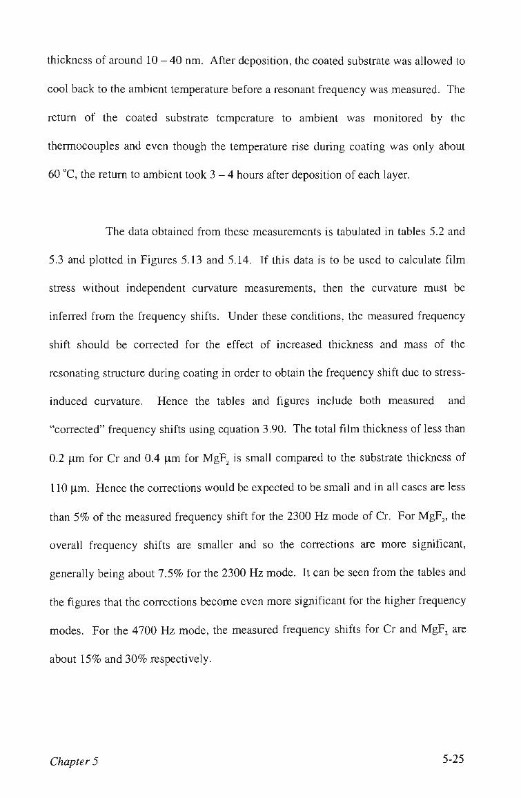
and data obtained from finite element modeling. These data are graphically represented
in figure 3.6. The differences between these sets of data is less than 1.3%. Therefore
Table 3.6 Comparison of calculated resonant frequencies, using equation 3.48 for a curved glass plate, clamped in the center, and data obtained using FEM. The frequency shifts shown are the differences in frequency between the curved and flat plates. The resonant frequency of flat glass was obtained using FEM method.
equation 3.48 has been used throughout this thesis in situations requiring an analytic
expression relating frequency shift to radius of curvature. Specifically it has been used
Chapter 3 3-22
to relate modal frequency shift to stress via a separate relationship between stress and
curvature (see section 3.8.2).
700
600
500
400
Freq
uenc
y sh
ift (
Hz)
o o
o o
100
0
1 r\r\ -100
1 k t I 1 I I 1 1 1 1 1 1
* FEM: Mode 2300
; • FEM: Mode 3400
* FEM: Mode 4700
^ Theoiy: Mode 2300
o Theory: Mode 3400
<!> Theoiy: Mode 4700
Z ^ -0
; \
d 0.5 1
i(m-
I 1 1 1 1 1 1
t
/ •
/ ' / ^ / <> / 9
1' / /
'/
1.5 2
1)
1 1 1 1
2300 Hz '
~
3400 Hz ;
4700 Hz '.
1 1 1 1
2.5
Figure 3.6 Variation of resonant frequencies for modes of about 2.3 kHz, 3.4 kHz and 4.7 kHz with inverse radius of curvature by EEM (open points) and theoretical calculations using equation 3.48 (solid points).
Chapter 3 3-23
3.7 Stress and strain relationships
This section discusses the concepts of stress and strain which are used to
characterise the elastic properties of the substrate-film stmcture. Stress and strain are
defined and these definitions are then used in section 3.8 to obtain the relationship
between stress and curvature for a shallow spherical shell.
3.7.1 Definition of stress and types of stress
A system of forces applied to the body produces a change in its dimensions.
The fractional change in dimension is called the strain in the body. The force per unit
area required to produce this strain is called the stress. If the surface of a solid is
subjected to external forces Pj, P^ and Pj as shown in figure 3.7, intemal forces, denoted
by F, will resist the deformation and maintain equilibrium. F will vary with position
throughout the body and the intensity of this force (force per unit area) at a point is the
stress at that point. Referring to figure 3.7, the resultant force on a small element of area
AA, cut perpendicular to the x axis, at point Q is represented by AF, and components of
AF along the x, y and z axes are AF , AF , AF . The stress components are defined as:
AF AF AF CT, = l im—f, T^ = l i m - f , T,, = l i m - f , (3.49)
^ M o AA ^ M o AA AAo AA
Chapters 3-24
where CT^ is the normal stress and x^ and \^ are the shear stresses. The normal stress is
the intensity of a force perpendicular to a cut while the shear stresses are parallel to the
plane of the element. By convention, normal stresses directed outward from the plane
on which they act (i.e. tension) are considered as positive stresses and normal stresses
directed towards the plane on which they act (i.e. compression) are considered to be
negative stresses.
Figure 3.7 Stress components in a solid.
In general, there are three normal stresses a , a , a , directed along the three
principal axes. There are also six shears stresses T , x . T, X , x„, x, where the first *• *• xy yx 2y yz zx xz
subscript denotes the axis perpendicular to the plane on which the stress acts and the
second provides the direction of the stress. In matrix form, the stress components appear
as stress tensor
r = cr. T xy xz
yx yz
vc zy
(3.50)
Chapter 3 3-25
Both the stress and intemal force components are used to describe the
intemal state in a solid. For a bar cut perpendicular to the x axis, as shown in figure 3.8,
the following relationships are valid (Pilkey, 1994):
F, = P = la,dA, (3.51)
Vy=hxydA, (3.52)
y-Vz-l^zdA, (3.53)
M.-T = \x^jdA-\x^zdA. (3.54)
M^My=\G^zdA, (3.55)
M,=-\^MA. A
(3.56)
Here cris normal axial stress (o;), Tis shear stress, P is axial force, Fis axial torque. Vis
vertical shear force {V) and M is bending moment.
Fx=P Mx > X
Figure 3.8 Intemal forces and stresses in a solid bar.
Chapter 3 3-26
3.7.2 Definition of strain
The application of external forces to an object can change the shape or size
(or both). The extent of this deformation determines its strain. Such strains can be
normal or shear. Normal strain is taken as positive when tensile forces elongates the
object and negative when the compressive forces contracts the object. When a force F is
applied along an object perpendicular to the cross section A as shown in figure 3.9(a),
intemal forces in the object resist the distortion. In this way the object attains an
equilibrium in which its length is increased by an amount AL from its initial value Lg.
The tensile strain in this case is defined as the ratio of the change in length, to the
original length
AL e, = — . (3.57)
When an object is subjected to a force F tangential to one of its surfaces
while the opposite surface is held fixed a shear stress is developed in the object. If the
object is a rectangular block, the shear stress results in a shape for which the cross-
section is a parallelogram as shown in figure 3.9(b). Under the action of shear stresses,
shear strains (y) are induced. Shear strain is defined by the tangent of the shear
distortion angle a in figure 3.9(b). In general, the dimensional changes at a point in a
body is determined by six strains, e 8 e , y^^, y , and y^^.
Chapter 3 3-27
(a)
^r-1^ q / %
i a
/w T:ZX
(b)
Figure 3.9 (a)Tensile force applied to a plate, (b) Distortion in a plate due to applied shear stress
For a bar of elastic material having the same mechanical properties in all
directions and under uniaxial loading, measurements indicate that the lateral
compressive strain is a fixed fraction of the longitudinal extensional strain. This fraction
is known as Poisson's ratio v and this relationship is expressed as
e, = -ve. (3.58)
Poisson's ratio is a material constant which can be determined experimentally. For
metals it is usually between 0.25 and 0.35.
Chapter 3 3-28
3.7.3 Elastic stress-strain relations
The stresses and strains are related to each other by properties of the
material. In the elastic regime, all strains are small and Hook's law dominates the
response of the system, so that for linear stresses
^x-Ez^, (3.59)
where E is Young's modulus. For a three-dimensional stress and strain. Hook's law for
an isotropic material can be expressed as
1
^ = F (3.60)
^.=iK-^K-^J]' (3.61)
e, = - [ a , - v ( a , - a J ] , (3.62)
T,y = GY,^ [i,j = x,y,z). (3.63)
Here G is the shear modulus. Volume changes are characterised by a bulk strain (change
in volume divided by original volume) and a corresponding bulk modulus, K.
Of the many different material constants (e.g., E, v, G, K) only two are
independent for an isotropic solid and the relations between these constants are (Kaye
andLaby, 1973):
E E EG
^ ^ 2 0 7 ^ ' ^ " 3 ( l - 2 v ) " 3 ( 3 G - F ) - ^^'^"^^
Chapter 3 3-29
In the sections which follow, some of the previous formulas will be used in obtaining
expressions relating stress in thin films to substrate deflection.
3.8 Relationship between stress in thin films and
substrate deflection
The formulae that have been used in almost all experimental determinations
to relate an average isotropic planar residual stress in a thin film to the resulting substrate
curvature are variants of an equation given originally by Stoney (1909) as
Ests
where / is the film thickness, R is radius of the substrate/film combination and E^ and t^
are the Young's modulus and the thickness of the substrate. This formula is applicable
providing that the film thickness is very much smaller than the substrate thickness.
However, in situations such as electrodeposition, the film thickness is often comparable
to the substrate thickness and any difference in Young's modulus of a film and a
substrate must be taken into account.
Brenner and Senderoff (1949) derived more general expressions which cover
most common experimental situations. As has been pointed out (Hoffman, 1966;
Davidenkov, 1961; Flinn, et al 1987; Ohring, 1992), these derivations neglect the effect
Chapter 3 3-30
of stress in two dimensions. When this is taken into account, the Young's modulus E^
needs to be replaced by the appropriate modulus for two dimensional deformation. The
correct formula is then
Ft' a , = -7 ^ T , (3.66)
where E^, t^, R, t^, are as defined previously and v the Poisson's ratio for the substrate.
The average stress Cyis defined by the relation (Klokholm, 1969)
' / 0
where afx) is the stress distribution through the film thickness t^ Experimentally, data is
usually obtained for the product o t^ as a function of film thickness t^ and the average
stress, cy, is then calculated from the slope of the line drawn from the origin to a point on
the curve representing a given film thickness. Hence, it is convenient to rewrite equation
3.66 as
F?^ Gftf = '' . (3.68)
If the radius of curvature of the wafer before deposition of the film was Rg than equation
(3.64) could be modified to (Sahu, et al, 1990 and Leusink, et al, 1992)
Ef ^/^/ = , (3.69)
R RJ 6(1-V J
where R is radius of curvature of the wafer after deposition of a thickness t, of thin film
Chapter 3 3-31
Equation 3.69 is sufficiently accurate for the most calculations of the stress
in thin films and it is valid under the following conditions:
(a) The substrate is linearly elastic, homogeneous and uniformly
thick.
(b) The bending displacement is small as compared with the thickness
of the substrate.
(c) The stress is uniform throughout the film thickness.
(d) No stress relief or changes in elastic constants take place as the
film is built up.
(e) The ratio t^ /1, must be < 10 With t^/1,> 10" and the ratio of
Young's modulus of film to that of the substrate > 1, the error in
equation 3.68 can be as large as 20% (Brenner and Senderoff,
1949).
In the following section the formulas for relationship between stress in the films and
substrate deflection for film/substrate system will be derived.
3.8.1 Determination of the stress in thin films
In deriving the equations for stress in the films, three cases will be
considered:
1. E=E=E t^«t^
Chapters 3-32
2. E=E=E r^-is thick (r^lju)
3. E^^E^ /'^-thick film
Case 1
It is assumed initially that the stress is anisotropic, F , = E^^^^^^= E^, t^«t^
and that the neutral axis lies in the middle of the substrate. Further, when the beam is
deformed the radius of curvature of the upper surface of the substrate/film system is
assumed to be the same as that of the lower surface (i.e. R»t^).
Consider the element of thickness dz at a distance z from the neutral axis as
shown in figure 3.10 (c). The strains 8 and 8 in the x and y directions are given by
e . - ^ and 8 , = ^ (3.70)
where R^ and R are radii of curvature of the substrate in x and y directions. The stress
and strain are related to each other by the properties of the material and for the case of an
elastic substrate equations 3.60 and 3.61 become:
B.=^K-va,), (3.71)
^.=^K-^^0' (3.72) i
where a and a are the stress components in x and y direction.
Solving equation 3.70, 3.71 and 3.72 for a, and a we obtain
Chapters 3-33
"' ^
tf
Fs ^ 4
t ts
i
Thin film ^^^
Ef
Es
Substrate
^ ^
Ff
-* ; Mf
- f) IVis
(a)
(b) (c)
Figure 3.10 Stress analysis of film-substrate structure: (a) composite structure; (b) elastic bending of structure under applied end moment, (c) an element of cross section of substrate/film structure.
ET (
\-v' 1 V,
— + — \K Ry J
and ^ ^ " l - V ^
f 1 V \
V ^> R^j (3.73)
Taking moments about the neutral axis, as shown in figure 3.10 (c), of film/substrate
stmcture (equation 3.55, M^= M) gives:
Chapter 3 3-34
2 <
| ^ = J -^fxdA= G^zdA , (3.74)
where o^ is the stress in the film in x direction. By substituting for G^ from equation 3.73
and using dA=dzdy, equation 3.74 becomes:
^+if
_ f E,z J -M5^dzdy=\ — 1 V, zdzdy . (3.75)
Hence
^fxhtf Et' s s 12(1-v;)
^ 1 ^
(3.76)
and
Gft^ EX
6(1-vj) K^x Ryj (3.71)
The y component of stress in the film, G is
^^^/ EX
6 ( l - v j ) (3.78)
If there is stress isotropic, a^ = a^ = a and R^=R^=R then equations 3.77 and 3.78
become
""''' 6 (1 -v j i ? (3.79)
Chapter 3 3-35
for a single film. If several films are present then the interaction of each film with
substrate can be treated separately. The total bending of the substrate is simply a linear
combination of the bending contributions of the films determined separately (Flin,
1989). To determine the stress in a particular film the inverse radius of curvature must
be determined with and without that film. This change in 1/R is then used in equation
3.73 to calculate the average stress in that film, therefore equation 3.69 should be used
for multilayer films.
Case!
Here it is assumed that F ,„=F „j , , =F and the film thickness, t^, is not
negligible in comparison with the thickness of the substrate, t^. The neutral axis will
now be at a distance (t^+t)l2 from the bottom of the substrate. Considering isotropic
stress, and taking moments as in Case 1:
ts+lf h-lf
J Gjzdz= JGzdz (3.80) t,-tf t,+tj
2 2
where G=G=G is the stress developed in the substrate.
Using the simplified form of equation 3.73 (for the case R=R=R), E,z
a = (3.81)
and integrating equation 3.80 we finally obtain
^ , f ^ i _ ^ . . (3.82) ^^ 6tXl-v)R
Chapter 3 3-36
This equation is identical to Brenner and Senderoff s equation (9), but differs from
Davidenkov's (1961) equation (2), which is
6R ^ftf= \ ^ • (3.83)
The origin of this difference hes in the simplified expression for bending moment used
in derivation of equation 3.82. Equation 3.82 reduces to equation 3.79 when t^ » t^
Case 3
When the substrate and the coating have different elastic moduli, Ej:^E^, and
the film thickness is not negligible in comparison with the thickness of the substrate, the
neutral axis no longer passes through (t^+t^/2. The position of the neutral axis must be
found by resolving forces. If it is assumed that the neutral axis is a distance Zg from the
bottom of the substrate. Then resolving forces, using equation 3.55, gives
Zn t,-Zo 's-^o+'f
\E,zdz- J E,zdz+ \E^zdz = 0, (3.84) 0 0 t,-Zo
where F = ' , and E,-
E2--
Es
1 - v /
Ef 1-v,
As before, v the Poisson's ratio and the subscripts s and/refer to substrate and film
respectively.
From equation 3.84 we get
Chapter 3 3-37
1+2E t +E r r r r r 1 + E t r r
(3.85)
where F^ = E^ /E, and t^ = tjt^. The assumption about the position of the neutral axis
made for case 1 and case 2 may now be verified by putting F^=l in equation 3.85. This
is identical to the result of Davidenkov (1961) who, also, derived the following
expression for stress in thin film:
G, =• E..t.
6(i-v.KJYT [\^2t^+EX)
(3.86)
AE^t^ + 6FX + AFt' + F;t^ 2 4 " ^ /
The integral in the denominator of this equation cannot be expressed analytically and
2^4 therefore numerical integration must be used for the final solution. If the term F^ t^ is
neglected in comparison with terms of lower order in t^ then the expression may be
integrated by expanding the dominator in the integral as a binomial. The result of this
integration is:
Gft^ = Et^
s s
6(l-vJ/? H - ( 1 - 2 F J , + Y ( 1 6 F , -Uy, - ( 4 F , -19F,^ + 1 6 F ; ) , ^
(3.87)
This formula reduces to equation (3.79) when tp'>t r^-f
The effect of the difference in elastic moduli is negligible when t>>t^, but
may be significant with thicker coatings (Brenner and Senderoff, 1949). The relations
given in equations (3.79) and (3.87) are only accurate for very small substrate
deflections, at least an order of magnitude less than the substrate thickness (Harper and
Chapter 3 3-38
Wu, 1990). Deflections of the order of the substrate thickness, or larger, provide
measurement advantages, but require higher-order analytical relations. A partially
nonlinear stress-curvature relation was developed for analysing the stress in an isotropic
thin film deposited on the substrate (rectangular) undergoing large deflections (Harper
and Wu, 1990; Masters and Salamon, 1993). It was shown that the nonlinear geometric
effect may be responsible for some of the discrepancies which have appeared in the
literature where different investigators have reported significantly different stress in the
same film material. Nevertheless, in the present work t^ » t^ (t^<2x 10^ for Cr films
and t^<4x 10" for MgF2 films) and equation (3.79) has been used to evaluate stresses in
thin films.
3.8.2 Relationship between stress in a film and measured resonant
frequency of the curved substrate/film combination
From equation 3.48 the inverse radius of curvature can be expressed as
I pf^^o^Zlkfl, (3.88)
Combining this equation with equation 3.79, the relationship between average stress,
thin film thickness and measured resonant frequency of the curved substrate/film
combination is given by
Chapters 3-39
O", = 3(1 ! t > ^^Af^n^s^-f^n^P^) • (3.89)
Thus it is clear that the average stress in a film can be determined by measuring the
change in resonant frequency which arises when a flat test substrate is curved by the
stress in the deposited film layer. This is the basis of the method for measuring stress in
thin films developed in the course of the work described in this thesis.
3.8.3 The effect of the coating material on resonant vibration
frequencies of a flat glass/film composite structure
Up to present, the equations for the frequency shifts associated with the
coating have all been derived with the implicit assumption that the thickness and mass of
coating are negligible in comparison with that of the substrate and the only effect is to
produce a curvature due to the stress. However, as can be seen from some of the
previous analytic expressions, the addition of a coating, even without any stress or
curvature change, will give rise to a small resonant frequency change due to the change
in total thickness.
In this section the effect of the thickness and Young's modulus of the thin
film on the resonant frequency of a flat substrate/film composite stmcture will be
considered. According to the equation 3.40 the allowed values of the resonant frequency
Chapter 3 3-40
of a flat plate depends on its thickness, density and Young's modulus. For a stmcture
comprising a substrate and coated film, a composite beam analysis needs to be employed
to determine the stiffness and resonant frequencies of the entire stmcture. To our
knowledge, no exact analytical expression has been obtained for the particular geometry
and mounting arrangement used in the work described in this thesis. However, an
expression has been obtained for the case of a simple cantilever and this may be used to
obtain approximate values of the frequency shifts caused by the coating in absence of
bending due to stress (Walsh and Culshaw, 1991). In this treatment, the resonant
frequency of the substrate/film combination, f ., is related to that of the uncoated
substrate,/„„(,, by
J mn{sf) _
J mn(i (.0 (3.90)
where "F is
¥ = •
4 + 6 ^ + - ^ ^ + 4 ts Eftf
ftA' EJt^'
\tsJ
+ •
K ^ s J
1+A^ \f
Eftfj 1+ Pfh
Psh )
(3.91)
Here the subscripts s and/refer to the substrate and film respectively and t, E and p are,
as before, the thickness. Young's modulus and density. The factor 'Ftakes into account
the extra mass and also the mechanical properties of the film on the resonant frequency of
the combined stmcture even if there is no stress at the film-substrate boundary. In order
to include the physical properties of the glass/film composite stmcture used in this work,
equation 3.48 could be re-written as
Chapter 3 3-41
J mn{s\ J mntpyr An^pR^
(3.92)
Table 3.7 shows the values of ^r^ for both Cr and MgF^ films calculated for
a range of film thicknesses typical of the experimental data. The used values for
Young's modulus are: E^,^=7.2xl0'° Pa, Ec=2.48xl0" Pa and E^^=l.llxlO'' Pa. The
data shows that in absence of stress, the coating has only a small effect on the resonant
frequency. However, when one is measuring frequency shifts, this effect can be a
significant fraction of the shift. This matter will be addressed further when the
experimental data is presented in chapter 5. In a situation where plate curvature cannot
be measured and stress must be inferred from frequency shift alone, this effect needs to
be considered. From Table 3.7, the variation in unstressed resonant frequency due to the
addition of a film should be less than 0.61% for Cr and 0.66% for MgF^.
Table 3.7 Calculated factor 'F (using equation 3.91) for film thicknesses up to 200 nm for chromium and 400 nm for magnesium fluoride.
film, indirect resistance heating was used. The evaporation material is placed in a
boat (12) made of tungsten (for evaporation of Cr) or tantalum (for evaporation of
MgF^). The boat, clamped between water cooled electrodes (13), is heated by
Chapter 4 4-4
electrical current flow and the material is evaporated on the substrate. The roughing
pressure (down to 10"' Pa) and total pressure were measured by means of Pirani and
Penning gauges, respectively. All depositions were carried out at about 10"'' Pa
residual gas pressure. The temperature of the substrates during coating was about
25°C.
Film thickness and the deposition rate during deposition were monitored
using a Maxtek TM-200 crystal thickness monitor. This monitor displays the film
o o
thickness in kA and the evaporation rate in A/s. A quartz crystal (oscillating at about
6 MHz) was placed in a holder (14) inside the vacuum chamber. The crystal was
gold plated on both sides to provide long lasting, non-corroding electrical contacts.
As deposition proceeds, the resonant oscillation frequency of this crystal changes
with respect to a reference oscillator. This frequency shift is proportional to the
thickness of the deposited film for thin films. The quartz crystal was mounted above
the boat adjacent to the substrate being coated.
The substrate holder can hold seven substrates during the coating process
as shown in Figure 4.2. The slot (16) for the quartz crystal on the substrate holder
was designed in a such a way as to compensate for the geometry-dependent
difference between deposition rate on the substrate and the rate on the thickness
monitor crystal. The speed of rotation of the substrate holder, during deposition, was
60 rpm. Substrate rotation was used for all measurements except those where
temperature and real-time deposition effects were being investigated. During these
measurements, the substrate was stationary.
Chapter 4 4-5
4.2.2 Chamber cleaning techniques
The vacuum system interior must be clean to achieve operating pressures
of 10""* Pa or better in reasonable times and to prevent contamination of the
Figure 4.2 Aluminium rotation substrate holder. The slot (17) is to allow deposition on the crystal monitor.
evaporated films. Visible contaminants such as deposits of coating materials were
removed by mbbing with emery cloth. This method is limited to robust components.
Delicate parts (ceramics, glasses and polished surface) were wiped with a clean lint-
free cloth as a preliminary step. Ethyl alcohol is very effective for removing water
Chapter 4 4-6
and trichloroethylene is used to remove oil and fingerprints from vacuum
components.
4.3 Sample preparation
The properties of a deposited film depend strongly on the adherence
between the substrate and the film. The quality of adhesion between a film and its
substrate depends to a large extent on the condition of the interfacial layer that is
formed between coating and substrate and this is influenced by a large number of
parameters. The interfacial bonding is strongly dependent on the choice of materials
for the coating and the substrate. Other factors affecting interfacial bonding are the
preparation of the substrate, the coating process and the handling of the
substrate/film combination after the coating process is completed.
4.3.1 Cleaning of substrate surface
The substrates used to test our technique were circular glass plates of
diameter 42 mm and thickness 0.11 mm as shown in Figure 4.3. Before a glass plate
can be coated with a thin film, all unwanted contamination must be removed from
the surface. If the substrate surface is not clean, then the film will not adhere well or
may not adhere at all. The adhesion properties of the deposited film depend strongly
Chapter 4 4-7
on the effectiveness of cleaning the substrates. The cleaning of the surface is
important but is also a very delicate operation with those very thin substrates.
Glass plate • Metal rod 1 support
-^ (p 42 mm
t 0.1 mm
Figure 4.3 The substrate used in experiments.
There are a number of cleaning techniques used in scientific and
industrial environments. Cleaning with solvents is a widespread procedure that is
always included whenever cleaning of a glass surface is needed. Our glass samples
were cleaned using the process developed by Kem and Poutinen (1970) for the
semiconductor industry. To remove organic contaminants the wafers were soaked in
hot trichlorethylene for 15 minutes. Two solutions are then used sequentially to
remove ionic and atomic contaminants:
1) The first solution was composed of a mixture of 5:1:1 by volume of
filtered deionised water, Kfl^ and anraionium hydroxide (NHpH). This
solution is used for 15-20 minutes at 75 - 85°C followed by a rinse in
deionised water.
2) The second solution contained a 6:1:1 by volume mixture of filtered
deionised water, H2O2 and HCl. This solution is used for 15-20 minutes
at a temperature of 75 - 85°C followed by a rinse in deionised water.
Chapter 4 4-8
The HjOj used was the unstabilized electronic grade. The wafers were
then dried in a vacuum furnace at a temperature of 90°C for 90 minutes. The clean
wafer was then placed in the aluminium holder as shown in Figure 4.4. A thin steel
rod of diameter 1.5 mm and length 25 mm was then glued in the centre of the rear
surface of the wafer.
Metal rod
Al lead J-
Counter-sink
Glass substrate
Figure 4.4 The jig used to glue the metal rod to the centre of the substrate.
4.3.2 The evaporants
Evaporation materials which were used included chromium, magnesium
fluoride and titanium. The chromium used for evaporation was supplied by CERAC
in 3-6 mm pieces and of 99.99% purity. Spectrographic analysis showed that it
contains less than 0.001 % of Ca, Mg and Si and less than of 0.0003 % of Fe. The
magnesium fluoride was supplied by SIGMA ALDRICH in 3-6 mm pieces and of
99.9% purity and titanium by PURE TECH as a plate of diameter 50.8 mm and
thickness 3.175 mm. The spectrographic analysis of these evaporants is shown in
Appendix A.2.
Chapter 4 4-9
4.3.3 Actual coating procedure
Usually, the curvature of a coated wafer is not completely uniform
because of the local variations of residual stress developed after deposition (Flinn,
1989). It is important for reproducible measurements that the same positions are
always used for LD excitation and curvature measurements. To ensure that this was
the case the sample was mounted in a holder which could be easily placed in a
reproducible position for coating or measurement. Once placed in this holder
(Figure 4.5), the sample was not removed until completion of all coating and
measurement steps.
The sample, mounted in its holder, was then placed in a diffusion
pumped vacuum chamber, the pressure was reduced to 2x10 ' Pa and the sample was
coated with first layer of about 10 nm chromium at a deposition rate of 10 A/sec.
The sample was then removed from the chamber and the curvature and resonant
mechanical vibrations were measured.
After measurement, the sample was replaced in the vacuum chamber and
additional layers of a thin film were deposited. Measurements were made on the
composite stmcture after each successive deposition until the glass plate had ten
layers of deposited material.
Chapter 4 4-10
Figure 4.5 The holder used to hold the sample during deposition of thin film and measurement.
4.4 Curvature measurement
The flat glass plate coated with a chromium thin film is transformed to a
concave spherical mirror due to the stress, as shown schematically in Figure 4.6. The
sample has a radius of curvature R and the center of the curvature is located at point
C. The principal axis connects the points C and S, where S is the centre of the
spherical segment. When a laser source is placed on the principal axis at point O and
the sample is translated by a distance Ax in the x direction than the resulting
translation of the reflected beam on the screen is A d. From simple geometry it is
readily shown that the radius of the concave sample is given to a good
approximation, by
R^2L-Ax
AK + Ad (4.1)
Chapter 4 4-11
Substrate (glass)
Figure 4.6 Schematic diagram of optical lever method used to measure the radius of the curved sample.
It should be noted that the average total sample thickness SE«L and has been
ignored. This approximation can introduce larger error in calculation of the radius of
the concave mirror when R and/or L are small while A x is large. The film stress was
calculated from the measured curvature using equation 3.66
^ / = Et^
s s 6{l-v)Rt,
For the curvature measurements, a low power (2.1 mW) He-Ne laser
light source (A = 633 nm) was used, although any suitable collimated light source
could be used. The test sample clamped to the aluminium holder was mounted on a
micrometer-controlled translation stage. The distance L from sample to screen was
4.23 m.
The accuracy in measuring the resulting translation of the reflected beam
on the screen (A <f) is limited by diffraction of the laser beam giving a diameter of
Chapter 4 4-12
the beam spot on the screen of approximately 6 mm (for the flat plate). The
translation of this spot (Ad) could be measured to within about 1 mm. Also, since
the wafer is generally not uniformly curved, the average radius of curvature is
obtained by making the measurement over a range of Ax values by translating the
mirror. The curvature and its standard error are then obtained by fitting equation 4.1
to the data. Using this method, the lever technique can give the average radius of
curvature with an uncertainty of approximately 2.5%.
4.5 Calibration of the film thickness monitor
The thickness of an individual film is an extremely important parameter
which figures in practically all equations used to characterise thin films. The
physical thickness is the step height between the substrate surface and the film
surface. Measurement of film thickness obviously cannot be accomplished in a
manner which does not affect the film using conventional methods for length
determination but requires special methods. A remarkable number of different, often
highly sophisticated, film thickness measuring methods have been developed and are
well reviewed in Maissel et al (1970). Two beam interferometry is appHcable to all
types of films and it has a high accuracy and also represents the most reliable
measuring method for the calibration of other techniques. This method, described by
Tolansky (1955) is based on measuring the distance between the interference fringes
formed by the multiple reflection of a beam of monochromatic light (often a sodium
Chapter 4 4-13
or mercury lamp) between a highly reflective film and a specially-coated Fizeau
plate which makes contact with the specimen at a slight angle and forms an air
wedge (Figure 4.7). The film must end with a sharp edge to achieve maximum
quality (sharp, high contrast, narrow) fringes. For such fringes, the film and
substrate must be coated with a highly reflective surface material.
The film thickness t^ is obtained by measuring the spacing AL and
displacement (L-AL) of the lines:
ALA t. = .
^ L 2
Our thickness monitor was calibrated using an Angstrometer (model
Nos. 980-4000 produced by VARIAN-Vacuum Division) using monochromatic light
from a sodium vapour lamp (A =589.6 nm). Suitable calibration samples were
formed on flat glass slides. The slides were prepared under similar conditions to the
thin film samples used in measuring the mechanical vibrations by the interferometric
technique. This means that the slides were cleaned using the procedure described in
section 4.3.1. Initially, all slides were coated with a 100 nm thick layer of chromium
to provide a flat and highly reflective surface. Then the slides were removed from
the vacuum chamber. A thin plate, made of brass shim, was then placed in contact
with the coated slide in a slide holder (Figure 4.4) in a such way as to mask half of
the slide. Then, all three slides were separately coated with different thicknesses of
chromium. The film thicknesses were measured using the Angstrometer and these
thicknesses were compared with the quartz thickness monitor readings. The stated
Chapter 4 4-14
resolution of the Angstrometer is better than ± 3 nm throughout the range of 30-2000
nm, so the calibration uncertainties were mostly due to random errors.
(a) Image plane
Mercury lamp
A
Beam-SpHtter
Reference plate
Interferometer —••
Partially transparent Ag film
Opaque Ag film
Film layer to Substrate be measured
(b)
Figure 4.7 a) Angstrometer - scope interferogram. AL is fringe spacing and L is fringe offset,
b) Schematic of optical apparatus for the measurement of the thickness of thin film fi-om multiple - beam Fizeau fringes. An opaque Ag film is deposited over a step in thin film.
Chapter 4 4-15
The slides were coated under similar conditions to the 110 p,m glass
substrates. Since the slides are more than 10 times thicker than the glass substrates
(1.5 mm), they do not bend appreciably as a result of the stress induced by the
coating. Even if some bending did occur, the Angstrometer results would not be
affected as it measures only the fringe change over a step with very small lateral
dimension. The resulting calibration curve for chromium thin films is shown in
Figure 4.8. The slope obtained from this graph has been determined to be
2.65±0.075.
4.6 Modal resonant vibrational frequency
measurements of the substrate/film system
The experimental arrangement which was used to excite and detect
mechanical vibrations of the glass sample, coated with a thin film is shown in
Figure 4.9.
For measurements in the atmosphere a 40 mW 830 nm Sharp LT015PD
laser diode was used to excite vibrations in the sample. This diode was placed at a
distance of approximately 250 mm from the sample. The output of the laser diode
was square wave modulated (50 % duty cycle) using a TTL driving signal from a
precision Hewlett Packard 33120A function generator. The output power of the
laser diode was controlled by a Sharp IR3C07 Laser Diode Driver integrated circuit.
Chapter 4 4-16
This circuit incorporated automatic control of the optical output power via feedback
from an intemal photodiode to control the laser drive current. The laser was
operated at an average power of 15 mW in order to keep it well below its damage
threshold. The laser diode was mounted on an aluminium heat sink to keep its
operating temperature well below its rated maximum of 50° C.
220
190 1) a. o o 4J
I 160 00
<
P
U 130
S c
c
2 100
70
- I f l i r t "• r —T—r—I—r—^~T-
20 4 0 ' • ' > • ' • i - _1-J I l_l L J I I I I I I L.
90
Film thickness (nm) measured by Thickness Monitor
Figure 4.8 Calibration curve for the quartz crystal thickness monitor.
Chapter 4 4-17
Function generator Laser diode
Cr film
Interferometer
Amplifier Drift compensator
Oscilloscope ^ Computer
Substrate (glass)
Metal rod support
Figure 4.9 Schematic diagram of the experimental set-up used to excite and detect vibrations in a glass wafer coated with a thin film.
For detection of resonance, the output of the interferometer was
monitored on the oscilloscope. Both the raw signal and the real-time EFT of this
signal were monitored on separate channels. The resonant frequency was
determined by adjusting the LD modulation frequency to maximise the amplitude of
the particular mode. Since the Q of the resonance was high, this method had no
difficulty in determining resonant frequencies to less 1 Hz. The resonant frequency
was temperature dependent through the temperature dependence of elastic moduli.
Thus fluctuations in ambient temperature were the limiting factor in resonant
frequency detection in a vibration free environment. In the vacuum system, pump-
generated vibration tends to limit the accuracy of resonant frequency determination
from the sampled vibration waveform but a figure of 1 Hz is a reasonable guide to
Chapter 4 4-18
the accuracy achieved. Variation of the modulation frequency by ± 0.5 Hz produced
easily detectable changes in the interferometer output signal. For resonant frequency
determination during a coating mn, the evaporation rate was kept low so that manual
changes could be made to the modulation frequency to confirm resonance at each
measured point.
For some measurements the resonance detection system was automated
by using a suitably filtered and amplified signal from the interferometer to modulate
the LD. Provided the filter has a sufficiently narrow bandwidth the resonant
vibration amplitude will grow from the initial vibration noise at the modal resonant
frequency. In this way the resonant frequency could be read using a frequency
light was also divided by DCl into two paths, one returning back to the laser, the
second forming the remainder of the interferometer's signal arm. The signal and
reference beams were then recombined using a second 2x2 1550 directional coupler
(DC2). Any change in air path between the sensing fibre tip and the vibrating
Chapter 4 4-29
reflective surface varied the path length of the signal branch with respect to the
reference branch, causing intensity modulation of the output of the InGaAs
photodetectors.
The optical path difference between the two arms must be less than the
coherence length of the light source. This was easily arranged in the interferometer
arrangement used as the coherence length of the 1523 nm laser was greater than 1
metre.
The separation between the fibre and the vibrating surface (open air
path) was typical about 20 cm. The two optical fibres (reference and signal arms)
were paired closely together and therefore were largely subjected to the same non-
signal perturbations. This tended to minimise the interferometer drift and reduce the
voltage needed on the piezoelectric phase modulator. The optical path length of the
each arm was 8 m.
The phase modulator was constmcted by winding 50 turns of single
mode fibre (standard Optix 1300/1550 nm communications fibre) around a piezo
electric cylinder (Tokin XOZ-138) of outside diameter 38 mm, inside diameter 36
mm and height 30 mm. This phase modulator was similar to that described by a
number of other workers (Kingsley, 1978; Jackson et al, 1980) and involved phase
change being induced into the reference fibre by a voltage-induced radial change in
the dimensions of the PZT which applied a longitudinal strain to the wound fibre.
The induced phase shift in these devices is given by (Digonnet and Kim, 1988)
Chapter 4 4-30
A(l)=^{lAn+nAl), (4.20) A
where An and Al are variations of the refractive index and the fibre length
respectively and X is the vacuum wavelength of laser beam. Martini (1987) gives a
detailed analysis of the phase modulation efficiency (milliradian V 'turn') which can
be obtained with PZT-type modulators. Kingsley (1978) and Jackson et al. (1980),
operating at frequencies well below the first mechanical resonance, obtained values
70 volt-tum and 100 volt-tum respectively for a 2n radian phase shift at 633 nm
using Vemitron PZT-5H ceramic piezoelectric transducers. These values are in
general agreement with what would be expected from the calculations of Martini.
In the arrangement described above using a Tokin PZT cylinder, the number of volt-
tums for a 2n radian phase shift can be approximately calculated. The voltage V
applied to the PZT, through the piezoelectric effect, causes the radius of the cylinder
to expand or contract an amount Ar^dp.^ where d^^^ is the piezoelectric coefficient
which is approximately 4.10x10"'° mV"' (Ohki, et al, 1992). The fibre attached to
the cylinder will be stretched by cylinder expansion and its increased length will
induce a phase shift in the propagating light. The fibre length extension is given by
AL=27iNAr where N is the number of turns. By neglecting variations of the
refractive index when the fibre is stretched (An=0) the equation 4.20 becomes
A^-^^^nNdp^jV. (4.21) A
For n=1.53 (for glass), N=50 and A=1523.2, we obtain
zi( = 0.792V (radian). (4.22)
Chapter 4 4-31
Hence, a phase change of 2Tt radians requires about 7.9 V. The piezoelectric
feedback used an 18 V power supply and this proved to be quite adequate for drift
compensation in a laboratory environment.
(b) Detector and feedback circuitry
The circuit diagram for the electronics used to detect the optical signal
from the interferometer and to drive the piezoelectric modulator is shown in Figure
4.16. The two output signals of the interferometer are in antiphase and subtraction
of these signals in a differential amplifier reduces the common mode noise and
improves the signal-to-noise ratio. Two InGaAs photo detectors (LYTEL 0981)
were followed by NE 5532 (Al and A2) low noise operational amplifiers used in a
transimpendance configuration. Further amplification was provided by LM347 low
noise amplifiers (A3 and A4) before the signal has subtracted in a further LM347
(A5). The electrical bandwidth of the detectors and associated amplifiers was DC to
100 kHz.
The output of A5 was integrated using another LM347 (A6) and the
output of this stage was used to drive the piezoelectric modulator. Provided the
output voltage swing from A6 is large enough, this signal can maintain the
interferometer at the quadrature point. The detector/feedback circuit was powered
using two 18V batteries. For noise isolation, the circuit and batteries were mounted
in a grounded metal box.
Chapter 4 4-32
5k6 10k 5k6
Lytel_ 0981
Lytel 0981;
to PZT
100k y \~^ 47k ^ 10k
Figure 4.16 Electronic circuit to detect optical signal from interferometer and to drive PZT.
(C) Calibration of the interferometer
The interferometer was tested and calibrated by using the Lutz-
Pickelmann piezoelectric mirror shaker (PZMS) type MB-ST-500/3. The PZMS
was biased at -(-250V and was modulated by an 300 Vp_p ac voltage at a frequency of
410 Hz. The detector output, V, is related to the displacement, Vj, by the relation
(Scmby and Drain, 1990)
^ = ^ D c + ^ o S i n (' Anr\^
A (4.23)
\ A J
where A is the wavelength, V is the amplitude of the interference signal and V^^ is
the DC bias signal. The proportionality constant between the output of the
interferometer and displacement depends on the optical signal levels and amplifier
Chapter 4 4-33
gains. Calibration under operating conditions is necessary for absolute measurement
of displacement. This was accomplished by switching off the PZT feedback and
using sufficient vibration amplitude on the PZMS to take the interferometer output
through a number of fringes. The peak interferometer signal voltage is then the
parameter V, in equation 4.23. When the feedback is restored and the vibration
amplitude of the PZMS is restricted so that the amplitude of the AC component of
the interferometer output is less than V^, it can be simply shown ( Scmby and Drain
1990) that the displacement rj is related to the output V by
A /V^ A V ri = — s m
4;r V 471 V, if V«Vg. (4.24)
The noise equivalent displacement, r]^, which is the displacement corresponding to
the RMS noise level, is given by (Scmby and Drain, 1990)
^ - = = 7 ^ ^ ' (4.25)
An Vo
where (V^) is the mean square noise at the output of the detector. The noise
equivalent displacement (NED) was found to be 0.16 nm with an electrical
bandwidth of 100 kHz.
A summary of characteristics and performance of the active homodyne
interferometer is given in Table 4.1. This interferometer is amphfier noise limited
and an appropriate performance figure of merit is the NED divided by the square
root of the bandwidth. The NED can be reduced by limiting the electrical bandwidth
of the detector electronics. This could have been done easily in the present work as
the signal frequencies of interest were generally less than 10 kHz. However, since
Chapter 4 4-34
the signal-to-noise ratio was more than adequate with the lOOkHz circuitry, no
attempt was made to limit the bandwidth. It should be noted that all calibration
measurements have been made using the PZMS with a fully reflecting mirror
mounted in the mirror shaker. This gives a high Vg for a given laser power and
hence a low NED for a given noise level. If a less reflecting surface is used, a lower
value of V would be obtained which would increase NED figure. The reflecting
surface from the samples used in this work was titanium film of 20 nm thickness.
This is a very good reflector and therefore during the experimental measurements
the NED figure was very close to value as stated in Table 4.1.
Table 4.1 A summary of characteristics and performance of the active homodyne interferometer used to measure the changes of resonant frequencies which are related to the changes in the stress developed in thin films.
Wavelength Detector Laser Total optical path length Air path length Bandwidth RMS noise Total NED NED/VHZ
1523.2 nm LYTEL 0981 (InGaAs) Melles Griot 05 SIP 871 (1.2 mW) 853 cm 20 cm X 2 100 kHz 5.7 mV 0.16 nm 5.06x10" m/VHz
4.7 Physical principle of the photothermal excitation
mechanism
The physical principles involved in the generation of mechanical
vibration using modulated laser beam are best understood by considering processes
Chapter 4 4-35
occurring in metals. When a modulated laser beam illuminates a small region of a
target, part of energy is absorbed by interaction of electromagnetic radiation with
the surface. This process depends upon the electrical and magnetic properties of the
material and the frequency of radiation. The remaining energy of the laser beam is
reflected or scattered from the surface. The absorbed electromagnetic energy is
converted to thermal energy resulting in a rapid rise in temperature. This
temperature rise in tum gives rise to transient thermoelastic stress and strain in a
very thin surface layer as the metal tries to expand. With heat diffusion, a time
dependence temperature profile develops in the sample (Opsal and Rosencwaig,
1982). This time-dependent variation of temperature between the illuminated and
rear (unilluminated) surface produces a modulated bending moment and thus the
sample flexes and begins to vibrate at the modulation frequency. If the modulation
frequency corresponds to a resonant vibration mode of stmcture, the amplitude of
vibration is significant.
Since the glass or substrates used in the work described in this thesis are
not strongly absorbing materials, the photothermal excitation can be greatly
increased by coating one surface of the substrate with a thin coating of metal which
is strongly absorbing at the laser wavelength used. This was generally achieved by
sputtering a thickness of about 20 nm of titanium onto the rear surface of the
substrate before deposition, on front substrate surface, of the film to be studied. The
heat generated in this rear surface film is transferred to the glass substrate causing it
to bend.
Chapter 4 4-36
4.8 Description of modified vacuum system
As described in previous sections, the all-optical technique developed
during this work allows indirect measurement of stress in coated substrates which
were removed from a vacuum deposition system. This technique was modified to
allow real-time measurements under controlled conditions inside a vacuum system.
This has permitted much more accurate and reliable measurements and is very easy
to implement as it only requires two optical fibre feedthroughs into the vacuum
system. For this purpose the vacuum system described in section 4.2.1 was
modified. Figure 4.17 shows a schematic representation of the vacuum coating
chamber and excitation/sensing systems for in situ monitoring the modal resonant
vibrational frequencies of the substrate/film system. The focussed and modulated
laser diode light, for photothermoelastic excitation of the sample, was delivered to
the substrate in the vacuum chamber via an optical fibre of core diameter 100 p,m
placed about 60 mm from its rear surface. The optical power incident on the sample
was 13 mW. Only the one sensing fibre of the interferometer was passed through a
feedthrough into the vacuum chamber (about 50 mm from the rear surface of the
substrate being measured). Vibration from the mechanical pump was minimized by
mounting it away from the coating plant. Figure 4.18 shows a typical FFT (Fast
Fourier Transform) trace of the output of the interferometer when the resonance at
about 3400 Hz was excited. This trace shows that most of the environmental noise
is at low frequency and the signal-to-noise is quite high for frequencies greater than
2 kHz. The mechanical and diffusion pumps were operating during these
measurements.
Chapter 4 4-37
Function generator
T Laser diode
Optical Fibres
im X XXM
Drift compensator
Interferometer
I Amplifier
Figure 4.17 Schematic diagram of evaporation plant with experimental setup for in situ measurement of stress in thin films: (1) Glass substrate; (2) Head of film thickness sensor; (3) Shutter.
Chapter 4 4-38
0.8
0.6
cu S < 0.4 -
0.2 -
3400 Hz
^iju__n«Aiftj_iftUiLiJuu. h_i _i_jL • • • I • • • • 1 • • • I • • • • 1 • • • 1 • • ' ' I ' ' ' ' I ' ' '
0 0.5 1 1.5 2 2.5 3 3.5 4
Frequency (kHz)
Figure 4.18 Typical output of the interferometer when the resonance at about 3400 Hz was excited. During these measurements all pumps were nmning.
4.9 Summary
The new fibre optic technique, described in this work, was first
demonstrated when the samples were coated with Cr thin films in vacuum system
and then removed for resonant frequency measurements under room conditions.
The operation and design details of the homodyne interferometric sensor and its
electronic signal processing circuit were described. This interferometer had a noise
equivalent displacement (NED) of 0.16 nm with a bandwidth of 100 kHz.
Chapter 4 4-39
For in situ measurements under controlled conditions the existing
vacuum system was modified to accommodate the fibres of the interferometric
sensor and photothermoelastic excitation systems. This modification requires only
two feedthroughs into the vacuum system. Vibration from the mechanical pump
was minimized by mounting it away from the frame of coating plant. The FFT trace
of the interferometer output showed that an excellent signal-to-noise ratio was
achievable during vacuum system operation for modes with resonant frequencies
above 2 kHz. The equipment described in this chapter was used to make
measurements with Cr and MgF^ films and the data obtained is presented and
discussed in the following chapter.
Chapter 4 4-40
Chapter 5
Experimental results and discussion
5.1 Introduction
The experimental techniques and corresponding stress equations,
described in the preceding chapters are, in principle, simple. However, the stress may
display variations as a function of deposition variables, the nature of the film-
substrate interface and film thickness. Important deposition variables include
substrate temperature relative to the melting point of metal, deposition rate, vacuum
residual gas composition and pressure and also angle of incidence of the vapour
beam. Data published by different investigators employing different measurement
techniques for stress determination are frequently inconsistent. The following trends
can be discerned from published results for stress in metallic and non-metallic thin
films:
(a) In metals coated on glass substrates, the film stress is tensile
with a magnitude ranging from 10 MPa to 2000 MPa.
(b) The magnitude of the stress in non-metallic thin films is
frequentiy small. It should be noted that while the most
metallic thin films are under tension, dielectric and
semiconductor films are generally in state of compression.
Metals with high melting points generally tend to exhibit
higher residual stress than more easily melted metals.
The experimental technique for indirect measurements of stress in coated
substrates, described in the preceding chapters, was initially tested using chromium as
the evaporation material. This chapter presents results for both chromium and
magnesium fluoride thin films. In the early work on chromium films, the samples
were coated in the vacuum chamber and then removed for resonant frequency
measurement in the atmosphere. This was followed by re-insertion into the vacuum
chamber and the cycle was repeated until a set of measurements had been made for
various film thicknesses. Since the surface of each layer was exposed to air, the
layers contain gaseous contaminants. To try to measure the extent of this problem, an
Auger Nanoprobe was used to determine concentration of principal species as a
function of depth. One further problem with these early measurements was that it
was not possible to measure the resonant frequency of the substrate before coating
commenced. This is due to the lack of any layer to act as an absorber for the
excitation laser beam before the first coating layer was applied. These early
measurements used the chromium layers themselves to absorb the laser modulation
and reflect the interferometer beam.
For subsequent measurements using both Cr and MgF^ films two
improvements were made:
Chapter 5 5-2
(a) A thin layer of titanium was applied to the rear surface of the substrate to
act as an absorber/reflector. This is a low stress layer, which does not
contribute significantiy to the overall stress/curvature of the samples.
(b) The measurements were made in situ in the vacuum system and so
atmospheric contamination between successive layers was not a problem.
The use of both atmospheric and in-situ measurement allows some quantification of
the effect of the atmosphere on the coatings.
5.2 Auger Nanoprobe Analysis and depth profiles
The radius of curvature and the resonant frequencies of the glass plates
were measured after depositing each successive layer of Cr and the stress of the
composite calculated using Equation 3.66. It should be noted that Equation 3.66
assumes a uniform homogeneous film and the removal of the test sample from the
vacuum chamber may produce a non-homogenous stmcture. Since chromium is a
reactive material, some surface oxidation is to be expected. In addition, gas
molecules incorporated into the lattice of Cr during deposition of the film may affect
the stress. While the bulk of the contamination should arise from the atmosphere,
organic molecules within the vacuum chamber originating from a diffusion pump oil,
vacuum grease, gasket materials and adsorbed gases can be also incorporated in the
lattice stmcture of the Cr during thin film growth as the base pressure of the vacuum
system was only about 10" mbar. To check the homogeneity of the films, the samples
were subjected to Auger Nanoprobe analysis.
Chapter 5 5-3
The Auger Nanoprobe detects and measures the Auger electron signals
from a sample (Ferguson, 1989). Auger electrons arise when an atom in the sample is
stmck by a fast-moving particle such as an electron and an inner shell is ionised. The
vacancy can be filled by another electron in the atom making either a radiative (X-
ray) or non-radiative (Auger) transition. The latter case can result in the emission of
an electron with kinetic energy which is uniquely defined by the energies of the levels
and which is thus characteristic of the ionised atom. Analysis of these Auger
electrons permits quantitative analysis of the composition of the surface of a material.
The Auger process is more probable than X-ray emission for energies less than about
3 keV and is strongest for lower atomic number elements
The energy of Auger electrons varies between about 10 eV and 2300 eV
(Ferguson, 1989) with a mean free path of about 0.4 - 4 nm, in metals. To achieve a
meaningful Auger analysis, in particular for low mean free path electrons, the
equipment must be capable of maintaining a vacuum of better than 10' Pa if the
surface is to be kept clean long enough for the analysis to be carried out. It is
generally necessary to clean the surface before Auger analysis is possible. This is
usually done by means of an ion etching device (ion gun) mounted in the apparatus.
The ion gun is also used to expose successively deeper layers for Auger analysis.
A depth profile of a wafer coated with eight layers of Cr was made using
the Auger Nanoprobe. During production of this film, the surface of each layer was
Chapter 5 5-4
s
ao c o
:=; w
1.1 w -a •a 2
3 2 C , - s
C ' " ^ • W _; ??
^ 2 - c O 6fi 3
S ^ s •a w c o
X
o
Ji-3 1=
^ D. O
I w ,
^ c o «.«'a X> o Pi
IS I O
c ao^ a 3 - X < 3 2 (D c« ™
I i S
(%) UOIJBXIU90U03 OIUIOJV
Chapter 5 5-5
exposed to air for several hours before further coating with additional layers. The
measured variation of atomic concentration with depth is shown in Figure 5.1. The
depth is given in terms of etching time (at a constant ion dose rate) and the measured
thickness of the deposited layers. This profile shows that some oxygen and carbon
are present near the surface of each deposited layer, as expected. The innermost
layers of Cr (near the glass surface) show the highest fractional oxygen content.
Although, only a few percent contamination is present at the film interface, the non-
uniformity of the film, which is evident in Figure 5.1, raises some doubts about any
interpretation of the stress as being characteristic of Cr films for the particular
samples used in these measurements (Abermann, 1990). Since the contamination
appears mainly at the film interface, in order to accurately measure Cr stress as a
function of film thickness, the sample would have to remain in a vacuum chamber at
all times to prevent oxidation.
5.3 Initial results with chromium films (measured in
air)
Before presenting data on stress measurements it is useful to clarify the
way in which the data is presented and the meaning of the stresses which are plotted
in the figures. Data on stress in films is normally presented in terms of force on the
thin film layer per unit width of the film. This is equivalent to the average stress in
the film times the film thickness since
Chapter 5 5-6
^f=- • (5.1)
Here, G^, F^ t^ and w^ are the average film stress, total force parallel to the substrate
surface, thickness and unit width of the film respectively. In the equation above the
symbols have exactly the same meaning as they did in chapter 3 where the various
relationships between stress and measurable parameters, such as radius of curvature
or frequency shift, were derived. In this chapter, figures will be presented as average
stress times film thickness or as average stress. For a constant film width, the force
divided by width (or average stress times thickness) is the parameter which best
represents the force exerted by the film on the substrate or vice-versa. For constant
force at the substrate - film boundary, the average stress decreases in proportion to
the film thickness.
The radius of curvature and the resonant frequencies of the glass
substrate/thin film combination were independently measured in the atmosphere after
depositing each successive layer of Cr and the stress of the composite stmcture
calculated using equation 3.66. The results of this calculation are presented in the
Table 5.1. Figure 5.2 shows the variation of radius of curvature as a function of total
film thickness. The curvature increases as the Cr thickness increases, showing that
the total force exerted by the film on the substrate is increasing with film thickness.
The relationship between radius of curvature and thickness is clearly non-linear.
Chapter 5 5-7
Table 5.1 Measured resonant frequencies of the first 8 vibration modes (fj as a function of film thickness (t ). The frequency shifts from the uncoated values (Af J are also given as are the measured radius of curvature (lever method) and the calculated average stress (a). This data was obtained by removing the sample from the vacuum chamber after each coating layer and making the measurements in air.
Figure 5.3 shows the relationship between change in resonant frequency
(as measured by the fibre interferometer) and inverse radius of curvature for a
selection of measured frequencies. In order to plot this data using a common axis,
the frequency shift is plotted rather than the actual frequency. No measurements
were made of the resonant frequency of the uncoated flat substrates so the frequency
shifts were roughly obtained by simply extrapolating the data and estimating the
Chapter 5 5-8
uncoated frequency from the intercept on the frequency axis. It should be noted that,
for all resonant modes, the relationship between the resonant frequency and the
a, 4J
I 3
u O
3
2 • a
I I I I I—I I I I 1 I I I 1 1 — I I I I f i l l
..J • • I L.
50 100 150 200
Film thickness (run)
250 300
Figure 5.2 Variafion of radius of substrate/film curvature with total deposited film thickness for a chromium film. The measurements were made in the atmosphere. The radius of the curature was measiued using lever method.
inverse radius of curvature is not a linear function and the uncoated resonant
frequency was difficult to determine with an uncertainty less than about 10%. All the
resonant frequencies of the sample varied systematically with wafer curvature and
thus any one of the modes could be used to determine the stress. The modes with
Chapter 5 5-9
frequencies of about 7.1 kHz and 9.8 kHz were not plotted in Figure 5.3 in order to
avoid cluttering up the figure. These modes showed similar monotonic variations of
i (--') Figure 5.3 Measured variation of resonant frequency shift with the inverse radius o
curvature measured using lever method for some different vibrationa modes. The data was obtained after each deposited chromium film laye was exposed to the atmosphere. The lines are a guide to the eye.
Equation 3.66 shows that for uniform films the inverse of the radius of curvature
should be proportional to the product of stress and film thickness. Figure 5.4 shows
some tjfpical plots of frequency shift as a function of this product.
Chapter 5 5-10
fc
500 I I I I I I — I — I — I — I —
400
-;3~ 300
o a u
(D 200
100
0
I I I I I — 1 - — 1 — r — I — I — I — I r I I I
• Mode B (1443 Hz)
o Mode D (3328 Hz)
9
0 100 200 300 400 500 600
Stress X film thickness (Nm"l)
700 800
Figure 5.4 The resonant frequency shift versus the product of thickness and stress determined via equation 3.66 for successive deposition of the chromium film measured in the atmosphere.
A typical plot of average stress as a function of film thickness is shown in
Figure 5.5. It should be noted that the error in the stress arises mostly from the
uncertainties in obtaining independent measurements of film thickness (using a quartz
crystal thickness monitor) and the radius of curvature (using the optical lever). The
current measurements of resonant frequencies were made after varying periods of
exposure of the films to the atmosphere (-2-3 hours) and should be seen as a proof of
this technique rather than as a measurement of stress in pure Cr thin films. The
Chapter 5 5-11
average stress, for our slightiy oxidised and contaminated films, shows a generally
decreasing magnitude with increasing film thickness.
5000
4500
4000
ao B 3500 >
3000 -
2500 L
I I I I I r i l l I r ' ' 1 t 1 r •• T- r—T "• 1 t I 1—r—
I J- T "* T
1 1 f ' f "
{ J u. J i_ J 1 1 i_
0 50 100 150 200
Film thickness (nm)
250 300
Figure 5.5 Stress as a function of film thickness for Cr films deposited on a glass substrate. The stress has been determined from the curvature of the glass plate using equation 3.66 and is measured in the atmosphere.
Chapter 5 5-12
5.4 Measurements of stress when the rear surface of the
sample was coated with a thin titanium film
The previous measurements suffered from two main problems:
(i) It was very difficult to obtain frequency shifts since the
resonant frequency of uncoated samples (starting
frequency) could not be obtained reliably by extrapolating
curves of unknown functional form,
(ii) The removal of the specimens from the vacuum system to
make measurements in the atmosphere led to
contamination of the film.
In the following measurements, changes were made to try to overcome the first of
these problems (later in this chapter, problem (ii) is also addressed). Glass substrates,
with the same dimensions as in previous experiments, were cleaned using the
cleaning process described in section 4.3.1. The rear surface of the plate was then
coated with 20 nm of titanium film by sputtering from a magnetron source. Then, a
metal rod was glued to the centre of the rear surface of the substrate using the jig
shown in Figure 4.4. The sample was then placed in an aluminium holder (shown in
Figure 4.5) and the curvature and resonant frequencies were measured using the
optical lever (section 4.3) and the inteferometric technique (section 4.6.3),
respectively. With careful attention to the process of coating of the titanium film and
gluing the metal road on the rear surface, an almost flat sample can be produced. No
significant movement of the reflected spot could be detected when the radius was
Chapters 5-13
measured by translation of the mirror (Figure 4.6) and application of equation 4.1. In
practical terms this means the radius was greater than about 120 m. The sample,
supported by the metal rod in an aluminium holder, was placed in the vacuum system
and the first layer of Cr was than deposited.
Again, the radius of curvature and the resonant frequencies of the sample
were measured in the atmosphere after deposition of each successive layer of Cr.
This process was repeated until the sample had been coated with eight layers of Cr.
During the process of coating the substrate, measurement of the radius of curvature
and resonant frequencies, the sample was not removed from the aluminium holder
Figure 4.5) but it was removed from the vacuum chamber after each layer was coated.
Figure 5.6 shows the variation of radius as a function of film thickness
and the shape of the curve is very similar to the curve shown in Figure 5.4. Figure 5.7
shows a typical relationship between change in resonant frequency as measured by
the fibre interferometer and inverse radius of curvature for a selection of measured
frequencies. The resonant frequency of the titanium-coated flat substrates was
measured, so the frequency shifts were obtained by simply subtracting this data from
the data when the samples were subsequently coated by Cr. All the resonant
frequencies varied systematically with wafer curvature. The data shows a monotonic
increase in resonant frequency with inverse radius of curvature.
Chapters 5-14
t 3 O
(4-1
o S 3
1
1 ' ' • 1 ' ' ' 1 » -
0 l__l I L—J I I I l_ ' • • •
20 40 60 80 100 120 140
Cr film thickness (run)
Figure 5.6 Variation of radius of substrate curvature, measured using the lever method, with Cr film thickness. The measurements were made by removing the sample from the vacuum system after each successive layer of Cr was deposited. Samples were coated with an initial 20 run layer of Ti in order to measure the resonant frequency before Cr deposition.
Figure 5.7 shows a plot of frequency shift as a function of substrate
curvature. A typical plot of average stress as a function of film thickness is shown in
figure 5.8. The stress for our partially oxidised films shows a much smother,
monotonically decreasing, curve with increasing film thickness than was the case
with the initial results (Figure 5.5). One likely reason for such behavior is that the
samples were exposed to air for no more than 40 minutes before further coatings.
Chapter 5 5-15
Therefore, the oxidation and contamination of the Cr film was likely to be
substantially reduced compared to the initial measurements reported in section 5.5.
250
Figure 5.7 Typical measured variation of resonant frequency shift with the inverse radius of substrate curvature (obtained using the lever method) for some vibrational modes of the samples coated with titanium on the rear surface The measurements were taken in the atmo^here after deposition of each chromium layer. The lines are merely a guide to the eye.
Chapter 5 5-16
7000
p 4000 -
> <:
40 60 80 100
Film thickess (nm)
120 140
Figure 5.8 Stress as a function of film thickness for Cr films coated on a glass substrate with titanium film on the rear surface. The measurements were made in the atmosphere.
Figure 5.9 shows some typical plots of change of frequency as a function
of the product of stress and film thickness. Again, frequency shift is used so that the
data for the two chosen modes may be displayed using the same axis.
Chapter 5 5-17
250
200
N 150 X
o c <L> 3
100
50
1 1
•
•
-
~
-
-
-
-
_
•
a
I • • • 1 1 f 1 — 1 1 —
• Mode E (2188 Hz)
A Mode F (5229 Hz)
t
i
I
A t
1 . . . . 1 . . . .
— 1 — 1 — 1 —
A
•
T 1 1 r
A
•
1
A -
•
•
-
-
50 100 150 200
Stress X film thickness (Nm'i)
250
Figure 5.9 Resonant frequency shift versus the product of thickness and stress determined via Equation 3.66 for a sample coated with titanium on the rear surface. The measurement were made for chromium films in the atmosphere.
The second set of atmospheric measurements is clearly superior to the
first in that the resonant frequency was determined before Cr coatings were applied
and also the exposure time to the atmospheric contaminants was reduced. However,
the two sets of results which are shown in Figures 5.2 - 5.5 and 5.6 - 5.9 are broadly
similar. These curves show generally monotonic variations when one parameter is
plotted against another but since there is obviously significant atmospheric
contamination (Figure 5.1) it is difficult to make quantitative conclusions about the
Chapter 5 5-18
nature of the stress in these Cr films. To obtain meaningful data would require
measurements made within the vacuum system so that atmospheric contamination is
not a factor. Such measurements are presented in the next section. The disadvantage
of making measurements inside a vacuum system is that it is not possible to make
meaningful independent measurements of radius (R) using the lever method for
comparison with the frequency shifts determined by the interferometer. These
atmospheric measurements certainly demonstrate that the frequency shifts
accompanying deposition of thin film coatings can certainly be measured and these
shifts represent another parameter which can be used to indicate changes in stress for
thin film coatings.
5.5 Experimental results for in situ measurements
In this section experimental results are presented for real-time
measurements on Cr and MgF2 films under controlled conditions inside a vacuum
chamber. However, under real deposition conditions, frequency shifts are also
produced by differential heating and non-uniform temperature distribution in the
sample.
Before coating the sample with a thin film, the effect of thermal cycling
was investigated for a number of glass/Ti substrates. For these measurements, the
substrate was placed in the vacuum system and exposed to radiant heat from an empty
evaporation boat which had previously been outgassed. The sample was placed 15cm
Chapters 5-19
above the evaporation boat. This distance was limited by the size of the bell jar of the
vacuum system. To obtain an indication of the surface temperatures of the substrate
during an evaporation cycle without affecting the resonant frequency, thermocouples
were placed about 1mm from the front and real surfaces. While these thermocouples
did not accurately record the surface temperature, they do show similar trends during
radiant heating and can be used to indicate when the surface has returned to its
original temperature following a heating/cooling cycle. It was found that the resonant
frequency of the substrate decreased when the temperature of the sample increased.
A typical plot of resonant frequency shift as a function of temperature for the front
surface (as indicated by front surface thermocouple) is shown in Figure 5.10. A
similar graph was obtained for the rear surface except that the temperature was lower
than the temperature of front surface by about a factor of two. The resonant
frequency shift is very sensitive to the temperature variations, mainly due to
temperature dependence of Young's modulus of the glass substrate (Kaye and Laby,
1973)
E^(T) = E,[\-a,{T-T,)]. (5.2)
Here F„ and a,, are the Young's modulus and its temperature coefficient at the ambient
temperature T,. The variation in Young's modulus with temperature produces a
negative modal frequency shift as the temperature rises. Using values of Eg and a,, at
room temperature for glass (Kaye and Laby, 1973) the approximate magnitude of the
changes observed agrees reasonably well with the shift shown in Figure 5.10. The
positive resonant frequency shift evident in the latter stages of the cooling cycle may
be due to the thermal stress resulting from the difference between the thermal
Chapters 5-20
expansion coefficients of the titanium film and substrate. The substrate will be bent
with a slight concave curvature due to small difference in temperature coefficients of
titanium film (0^^=8.6x10^ K"'; Ohring, 1992) and substrate (a^,^,„,^=1 AxlO'^ K"', see
Appendix I). The different paths followed by the heating and cooling phases of
Figure 5.10 are probably due to the very different timescales associated with the
heating and cooling temperature changes.
fe
50
- #
£ -50
I ^ -100
-150
-200
I I I I I T 1 I I—r—T—r- ' I ' ' ' '
Mode B (3400 Hz)
Heating
J-L.
Cooling
• • t • • . • I • • . . I . . 1 1
20 30 40 50 60 70 80 90
Temperature ^C)
Figure 5.10 In situ measured variation of resonant frequency shift of the glass sample coated with titanium on rear surface, versus temperature.
The temperature measurements were made using a thermocouple near the front substrate surface.
The thermal cycling, previously described, was repeated three times on
each sample for a number of glass/Ti substrates. Similar graphs to that shown in
Chapter 5 5-21
figure 5.10 were obtained on each occasion. From this figure, it is clear that the
frequency shift always returns to the initial point after the process of heating and
cooling a glass/Ti substrate. This indicates that the thermal cycling process of the
samples is reversible and it does not change permanently the resonant frequency of a
substrate. Therefore, one can conclude that temperature rises accompanying the
deposition of the thin film do not affect the final measured resonant frequency shift of
the substrate/thin film stmcture provided the stmcture is allowed to first retum to
ambient temperature. When all measurements are made at the same uniform
temperature, frequency shifts are due only to changes of the curvature of the substrate
caused by the stress in the deposited thin film. If frequency shift measurements are
made during a continuous deposition, then some thermal changes will be present and
hence a component of the observed frequency shift will be thermal in origin.
Figures 5.11 and 5.12 show the measured variation of resonant frequency
of the 3400 Hz mode as a function of film thickness for chromium and magnesium
fluoride films respectively. These measurements were made in real time during the
continuous film deposition and hence will contain some thermal effects. For these
measurements, no shutter was used and the evaporation current was slowly raised
while the substrate was exposed to the radiant heat. Hence the resonant frequency
initially decreased due to the temperature rise before any coating occurred. Once the
coating commenced, positive (stress-induced) frequency shifts occurred. The shift as
a function of film thickness for one continuous coating mn is shown in the figures.
For this data, the deposition rate for chromium was about 10 A/sec and for
magnesium fluoride about 40 A/sec. It is estimated from the frequency shift before
Chapter S 5-22
coating commences that the temperature of the front and rear surfaces during coating
was between 90-120 °C and 40-80°C respectively. During film deposition, the
resonant frequency of the film/substrate composite will increase mainly due to the
changes in the curvature caused by the residual stress developed in thin film. Figures
5.11 and 5.12 show a fairly linear variation of frequency shift during coating with
film thickness. The fact that the slope is constant during deposition is a good
indication that the thermal stress and substrate temperature did not vary significantly
during the coating. This was confirmed by the thermocouple monitors.
0 1 I • I I • I • I • i • I • • • I ' ' ' I ' ' ' I ' ' ' I
-50
(Hz
<tt 2 c/l
>. U a aj 3
-100
-150 fe
-200
-250
Mode B (3400 Hz)
I I I I - ' • • • I • i_ i_ f ' I I i_i ' • '
0 20 40 60 80 100 120 140 160
Film thickness (nm)
Figure 5.11 Measured variation of resonant frequency shift with film thickness during the deposition of chromium. Under these conditions temperature changes also occur.
Detailed interpretation of the previous set of results is complicated by the existence of
stresses produced by both thermal and thin film effects. In order to avoid this
Chapter S 5-23
problem, further sets of measurements were conducted for which all frequency
measurements were made at the same ambient temperature and hence thermal effects
50
0
-50
"S -100 o
tI-(
Mode (3400 Hz)
•150
-200
-250 • • • ' X
0 100 A. _J
200 300 400
Film thickness (nm)
500 600
Figure 5.12 In situ measured variation of resonant frequency shift during the deposition of MgF2. Under these conditions temperature changes also occur.
should not be present. For these measurements a shutter was used to control coating
and shield the substrate from radiant heat when coating was not in progress. The
measurement technique involved sequential deposition of eight layers, each with a
Chapter 5 5-24
thickness of around 10 -40 nm. After deposition, the coated substrate was allowed to
cool back to the ambient temperature before a resonant frequency was measured. The
retum of the coated substrate temperature to ambient was monitored by the
thermocouples and even though the temperature rise during coating was only about
60 °C, the retum to ambient took 3 - 4 hours after deposition of each layer.
The data obtained from these measurements is tabulated in tables 5.2 and
5.3 and plotted in Figures 5.13 and 5.14. If this data is to be used to calculate film
stress without independent curvature measurements, then the curvature must be
inferred from the frequency shifts. Under these conditions, the measured frequency
shift should be corrected for the effect of increased thickness and mass of the
resonating stmcture during coating in order to obtain the frequency shift due to stress-
induced curvature. Hence the tables and figures include both measured and
"corrected" frequency shifts using equation 3.90. The total film thickness of less than
0.2 |Lim for Cr and 0.4 |xm for MgF^ is small compared to the substrate thickness of
110 |j-m. Hence the corrections would be expected to be small and in all cases are less
than 5% of the measured frequency shift for the 2300 Hz mode of Cr. For MgF^, the
overall frequency shifts are smaller and so the corrections are more significant,
generally being about 7.5% for the 2300 Hz mode. It can be seen from the tables and
the figures that the corrections become even more significant for the higher frequency
modes. For the 4700 Hz mode, the measured frequency shifts for Cr and MgF^ are
about 15% and 30% respectively.
Chapters 5-25
Table 5.2 Measured and corrected resonant frequency shift for Cr thin film for three different resonant modes.
(nm)
14.8 37.4 62.8 84.8
107.5 129.8 152.4 181.9
Mode 2300 Hz
iDcasarcd
(Hz)
23.9 62.4
109.2 150.1 193.9 234.9 279.1 338.5
coTTEcteil
(Hz)
22.8 59.6
104.5 143.7 185.8 225.2 267.7 324.9
A (Hz)
1.1 2.8 4.7 6.4 8.4 9.7
11.4 13.6
Mode 3400 Hz
mwDrEd
(Hz)
21.5 48.6 83.6 114
145.6 177.7
210 255
Af , (Hz)
19.8 44.4 76.5
104.4 133.5 163.1 192.9 234.6
A (Hz)
1.7 4.2 7.7 9.6
12.1 14.6 17.1 20.4
Mode 4700 Hz
meaxaiEd
(Hz)
12.3 36.6 60.3 85.9
108.6 135.2 161.2
196
comcted
(Hz)
10.0 30.7 50.4 72.6 91.7
114.9 137.4 167.6
A (Hz)
2.3 5.9 9.9
13.3 16.8 20.3 23.8 28.4
Table 5.3 Measured and corrected resonant frequency shift for MgF^ thin film for three different resonant modes.
Vilm
(nm)
15.0 52.4
100.7 157.7 213.5 267.8 329.5 396.2
Mode 2300 Hz
measored
(Hz)
4.8 26.8 51.1 76.6
106.5 133.1 162.2 192.6
corrected
(Hz)
4.2 24.8 47.2 70.6 98.4
122.9 149.7 177.6
A (Hz)
0.6 2.0 3.8 6.0 8.1
10.1 12.5 15.0
Mode 3400 Hz
measured
(Hz)
5.0 19.1 36.2 55.6 73.6 92.9
115.6 139.6
Af ^ (Hz)
4.1 16.1 30.4 46.5 61.3 77.5 96.7
116.9
A (Hz)
0.9 3.0 5.8 9.9
12.3 15.4 18.9 22.7
Mode 4700 Hz
measured
(Hz)
5.1 13.6 25.5 38.8 53.5 67.6 86.4
103.6
COIRClcd
(Hz)
3.9 9.4
17.4 26.2 36.4 46.2 60.1 72.0
A (Hz)
1.2 4.2 8.1
12.6 17.1 21.4 26.3 31.6
Figures 5.13 and 5.14 again show a linear variation of frequency shift
with film thickness as was the case for the continuous deposition measurements
shown in figure 5.11 and 5.12. Direct comparison of the two data sets is complicated
by the fact that the same substrate was not used for all measurements. However the
substrates were nominally equivalent yet the slope of the measured frequency shift for
the continuous coating case was significantly higher than was the slope for the
sequential deposition case. For the 3400 Hz mode of Cr these frequencies were about
1.5 Hz/nm (continuous) and 0.35 Hz/nm (sequential). For MgF^ the corresponding
frequencies were 0.5 Hz/nm and 0.35 Hz/nm. It may be that these differences in
Chapter S 5-26
slope indicate some difference in stmcture (and hence stress) for films deposited
under different conditions (temperatures and time).
N
3
u a u
350
300-
2 5 0 -
200-
150-
100-
50
r >
•
•
•
-
--•
------
--_
•
. -
•
• M
r
1
D
•
0
A
A
u
1 1 1 1 1 1 1 1 1 1 1 —
Measured data (Mode 2300 Hz)
Corrected data (Mode 2300 Hz)
Measured data (Mode 3400 Hz)
Corrected data (Mode 3400 Hz)
Measured data (Mode 4700 Hz)
Corrected data (Mode 4700 Hz) /
/2 / / / ^
// / ^ / / / ^
/% ^/ y /'7A // . / y y M .^' Ay^ /^ / / ° / / / ^^ yy^
/'^^/y /p ^^yy /Ay yz _ u 1 1 • • 1 — 1 — 1 1 1 1
1 1 1 1 , , -
/ /
/ / -/ /
m /
/ / 9
/ / * /
/ / p y
/ y
y^ yy^
, .
•
. -
•
1 1 1 1 1 1 .
50 100
Film thickness (run)
150 200
Figure 5.13 In situ measured variation of resonant frequency shift with film thickness of chromium for sequential deposition of layers. The substrate was allowed to cool back to room temperature before resonant frequency measurements are made. The lower line for each mode shows the frequency shift after correction by factor *Pi/2.
Figure 5.14 In situ measured variation of resonant frequency shift with film thickness of magnesium fluoride for sequential deposition (constant temperature for measurement). The lower line for each mode shows the frequency shift after being corrected by factor ¥^'2
Figures 5.15 and 5.16 show the average stress as a function of thickness
for Cr and MgF^ films. These figures are calculated using equation 3.89 and the
3400 Hz mode data of tables 5.2 and 5.3. Note that the calculated stress should be
independent of which mode is used for the calculations and in fact very similar data is
obtained for all measured modes. Figures 5.15 and 5.16 show data calculated using
both measured and corrected frequency shifts and the variation of average stress with
thickness for these two cases is quite similar. Correction of the data to allow for the
Chapter S 5-28
thickness and mass of the coating results in a decrease of the calculated stress by less
than 10% for both Cr and MgF^ films.
Figure 5.17 shows another plot of average stress against film thickness
for Cr and MgF^ films. Here the data is plotted on a log-log plot and the results are
excellent straight Hues with slopes and standard errors of -0.497±0.009 for Cr and
-0.496±0.003 for MgF^. Thus for this thickness range of these films, which are
deposited within the vacuum system without atmospheric contamination, the average
stress varies as JtJ. Although no independent measurements were made of the
curvature as a function of film thickness, this stress variation, together with equation
3.66, suggests that the curvature varies as JtJ. This result is consistent with the
linear variations of resonant frequency with film thickness (Figures 5.13 and 5.14).
A log-log plot of the radius data for sequential layers measured in the atmosphere
(Figure 5.17) appears to confirm this result with the slope of -0.489 ±0.0187.
Appropriate re-plotting of data presented by Klokholm and Berry (1968) for Cr films
of thickness up to about 150 nm on glass substrates shows a slope very close to - 0.5.
A similar result is obtained using the data of Pulker (1984) for Cr films of thickness
up to 100 nm, again on a glass substrate. It should be noted that this .JtJ variation
does not apply to all types of films, with much more complicated variations being
observed with other films and thickness ranges (Klokholm and Berry, 1968). The
Chapters 5-29
6000 r
5000
jg 4000
S O
> <
3000
2000
1000
"1 1 1—1 1 1—I—I r "I 1 1—I—I 1 — r
Corrected Mode B (3400 Hz) Mode B (3400 Hz)
A
• • • •
A
' ' ' • • ' • • ' • ' • ' ' '
50 100 150
Film thickness (nm)
200
Figure 5.15 Stress as a function of film thickness for sequential deposition of a Cr film at room temperature in the vacuum system. The lower
points (full circles) have been corrected using the \\i^''^ factor.
magnitudes of the stresses measured in this work are somewhat higher than those
reported by these other workers. Pulker (1984) gives a value for stress in Cr/glass
films which ranges from 2300 MPa to about 1300 MPa at 100 nm. Klokholm and
Berry (1968) give figures varying from about 1600 MPa down to 850 MPa at 100
nm. The figures obtained in this work are about 2000 MPa for a 100 nm Cr/glass
film. These differences are probably a result of the deposition parameters, which are
different for all three studies.
Chapter S 5-30
3000 " I ' ' I I ' ' ' ' I ' ' ' ' I ' ' ' ' I ' ' ' ' I ' ' ' ' I ' ' ' ' I ' '
2500 (M
Pa)
stre
ss
rage
>
2000
1500
1000 -
500
A • Corrected Mode B (3400 Hz)
A Mode B (3400 Hz)
A
A
50 100 150 200 250 300 350 400
Film thickness (nm)
Figure 5.16 Stress as a function of film thickness for sequential deposition of an MgF2 film at room temperature in the vacuum system. The lower points (full circles) have been corrected using vj/i/2 factor.
Figure 5.18 shows the variation in stress in an MgF^ film when exposed to
the atmosphere while still inside the vacuum system. These measurements show a
very rapid reduction in stress by about 40% in a few minutes followed by a slow
approach to an equilibrium value over a period of 2 - 3 hours. This is in agreement
with the data obtained by Pulker (1982) who observed that the stress in thin MgF^
film is reduced between 40% and 100% due to water vapor absorption.
Chapter S 5-31
9.6
9.4
9.2
o
9.0
8.8
I I I I I I I I
Cr-film
CT/~t/
n = - 0.497 ± 0.009
MgF2 film
a/~t/ n = -0.496 ± 0.003
g ^ ^ I 1 1 • • I • • 1 • I • • • • ' •
-7.6 -7.4 -7.1 -6.9
log(t/)
-6.7 -6.4 -6.2
Figure 5.17 Variations of average stress with film thicknes for sequential deposition of chromium and magnesium fluoride films in the vacuum system. The resonant frequency was corrected by factor \|/l/2.
Also shown in figure 5.18 is a similar curve obtained after heating the previous film
in vacuum for one hour at 150°C, then cooling back to ambient, followed by re-
exposure to the atmosphere. Clearly non-reversible changes have occurred as a result
of the initial heating and exposure to the atmosphere. Subsequently the film was re
heated in vacuum and exposed to the atmosphere a third time. On this third occasion
the variation of stress with exposure time closely followed the previous curve (second
Chapter S 5-32
exposure). Hence it appears that the stmcture of the film is not further affected by
subsequent heating/cooling/exposure cycles after the first.
> <
500
450
400
350
300
250
A.
%.
A A
I
• • • •
200' ' • ' ' _i L _l I I l _ _ l I I L.
0 2000 4000 Time (s)
6000 8000
Figure 5.18 Stress variation produced by exposure of a 518 nm thick MgR film to the atmosphere:* -on exposure of anew film to the atmosphere; * - on re-exposure of the previous film to the atmosphere after heating in vacuum at 150 C for 60 min.
5.6 Summary
In summary, a change in stress in a film deposited on a substrate gives
rise to a change in curvature of the substrate. By using a thin glass test substrate, this
curvature can be made relatively large and easy to measure. Curvature of the
Chapter S 5-33
substrate changes the characteristic resonant modal vibration frequencies. These
modes can be excited thermoelastically using a low power laser diode and the modal
frequencies measured remotely using a fibre optic interferometer. This method was
initially tested using a chromium film consisting of a series of layers with the coated
sample removed from the vacuum chamber for measurement after each layer. The
chromium film in these atmosphere measurements was uniform over the substrate but
non-homogeneous because of the presence of oxidation/contamination at the interface
of intermediate layers. By deposition of an appropriate thickness of titanium film on
the rear surface of the sample it was possible to measure the resonant frequency of the
flat glass plate before coating the chromium film on the front side. Hence, the change
in resonant frequency was determined more accurately than was possible by using the
cmde extrapolation to zero thickness used in the initial measurements. Finally, this
technique was adapted for in situ measurements and experimental results for the
chromium and magnesium fluoride films were presented. The effect of film thickness
on resonant frequency changes was also considered and it was shown that this effect
could be significant particularly for higher frequency resonant modes.
The results of this chapter have demonstrated that the combination of
photo-thermoelastic vibration excitation and measurement of the modal frequency
changes using a fibre interferometer, does represent a viable new technique which can
be used for the measurement of stress in thin films. This measurement technique is
broadly similar in difficulty of incorporation into a vacuum system to the current
common technique of measurement of film thickness using a quartz crystal thickness
Chapter S 5-34
monitor. Hence it should be capable of finding significant applications when properly
engineered instmments are commercially available.
Chapter S 5-35
Chapter 6
Conclusion
6.1 Conclusion
The aim of this project was to develop an interferometric optical fibre
sensing system which could measure the resonant vibrational frequencies of
substrates coated with thin film materials and assess whether such modal frequency
measurements could be used for the determination of stress in the films. The method
developed used substrates in the form of thin circular disks which were supported by
a rod fixed to the centre. Stress effects due to atomic mismatch between substrate
and coating resulted in a curvature of the substrate/film stmcture which produced
changes in the modal resonant frequencies. In order not to have the modal resonant
frequencies affected by the excitation and measurement system, it was necessary to
ensure that there was no mechanical contact between these systems and the vibrating
stmcture. This was achieved by coupling the remote interferometric vibration
detection system with remote photothermal excitation of the stmcture using a low
power laser diode.
An actively-stabilised homodyne optical fibre interferometer was
developed for this work. The interferometer was based on a 1523 nm He-Ne laser
and used a cylindrical PZT fibre stretcher in the reference arm for quadrature
locking. Despite the losses associated with injection of the laser light into single
mode fibre and the incorporation of an air path to the target surface, this
interferometer achieved a NED of 0.16 nm in a 100 kHz bandwidth. When coupled
with the photothermal excitation, this inteferometer allowed vibration frequency
measurements to be made with excellent signal to noise ratios.
The differential equations for a flat uniform circular disk supported at its
center were solved to obtain analytical expressions for the modal resonant
frequencies. These solution were then extended to cover the case of a thin spherical
shell - the shape of the stmcture after it begins to curve under stress. Finite element
analysis was used to confirm the predictions of the analytical expressions.
Expressions were also derived which related average film stress to the physical
dimensions, elastic properties, and resonant frequencies of the flat and curved
stmctures. To the knowledge of the author, these expressions are new and have not
previously been reported in the literature.
Measurements were initially made using metallic (Cr) films. The
variation of stress with thickness was determined by evaporating a series of Cr layers
in a vacuum system and removing the stmcture after each deposited layer so that
modal frequencies and curvature could be determined by measurements made in the
atmosphere. These measurements suffered from difficulties associated with
contamination of the layers while removed from the vacuum system. A further
problem was encountered with the difficulty of determining the modal frequency
before deposition when there was no coating to absorb the modulated LD excitation
beam used to photothermally excite the vibrations. These problems were overcome
by applying a very thin low-stress Ti layer to the rear surface of the substrate and by
Chapter 6 6-2
modifying the system so that measurements could be made in situ during
evaporation. Using this arrangement stress measurements were demonstrated for
both metallic (Cr) and dielectric (MgF^) films.
Substrate temperature rises during evaporation were shown to produce
significant resonant frequency shifts, due principally to the temperature dependence
of the elastic constants of the materials. These temperature effects represent a
significant limitation to stress determination unless the temperature of the substrate
remains constant during evaporation of else the substrate is allowed to cool back to
ambient before modal frequency measurements are made. Measurements made in
the vacuum system for both Cr and MgF2 films showed that over the thickness
ranges used, the average stress (and hence curvature) vary as the inverse square root
of the film thickness. Changes in film stress on exposure to the atmosphere for
MgF^ films were demonstrated by admitting air to the vacuum system after
deposition.
This work has added a new technique to ranges of techniques available
for stress measurements in thin films. The experimental systems required for its
implementation are reasonably simple and easily incorporated into a vacuum coating
system. With feedback from interferometer to LD excitation, it was demonstrated
that the system can be locked to resonance and the resonant frequency read directly
from a frequency counter. While very accurate measurements of resonant
frequencies are possible with the interferometer, in practice the accuracy of
determination of stress changes are limited by the temperature variations of the
stmcture during measurements. Absolute stress measurements are less accurate than
measurements of changes in stress due principally to the difficulty in determination
Chapter 6 6-3
of the resonant frequency of the flat glass plate prior to coating and the effect of
dimensional-related frequency changes during coating.
6.2 Future work
The new stress measurement technique described in this thesis has been
tested only with one metallic and one dielectric thin film deposited using resistive
evaporation under vacuum conditions. For these films the thickness range covered
was up to 400 nm. There is scope for further testing with a wider variety of single
and multilayer films, deposition techniques and film thicknesses. For maximum
benefit, such tests should be carried out under conditions where the optical technique
can be compared to other established techniques such as curvature determination via
interferometric displacement measurement.
In addition to basic studies such as those described above, it is a
relatively simple matter to properly engineer an instmment which utilises feedback
from interferometer to LD excitation to provide direct frequency readout. Such an
instmment could be used in practical situations where existing techniques are
proving difficult to apply or where their performance is less than fully satisfactory.
One such situation would involve applications to the semiconductor industry to
monitor stress during epitaxial growth or during metallisation coating applied to
silicon or other substrates. For example, one large semiconductor company uses a
process involving the deposition of Cr, Ni-V and Ag layers on thin silicon wafers for
metallic contacts. Currently there is significant wastage during dicing and separation
of these substrates as a result of stress-dependent curvature developed during
Chapter 6 6-4
coating. The optical technique would be more compact, accurate and simple to
apply than the existing optical lever stress monitor used in this process.
Chapter 6
References
Aberman, R. 1990, Measurements of the intrinsic stress in thin metal films. Vacuum,
vol 41, no. 4-6, ppl279-1282.
Bauer E and Popa H., 1984, Thin Solid Films, vol. 121, pp. 151.
Beck U., Smith DT., Reiners G and Dapkunas SJ., 1998, Mechanical properties of
variation, e.g. this guaranties microatome sections are evenly covered.
MENZEL cover slips are resistant to water (hydraulic class 1) and fulfill
all known standard requirements, particularly German Industrial Standard 12111.
Spacemens covered with MENZEL glass can be stored for long time periods for
examinations or documentation.
MENZEL cover slips contain neither lead, cadmium or thallium
compounds nor arsenic-oxide. If stimulated within the near UV-range, i.e. SitX = 365
nm (Hg) as in fluorescant microscopy, MENZEL cover glass does not show any
fluorescence.
The average coefficients of thermal-expansion are: (73-74)xl0"^ K' in the
temperature range of (20 - 300)°C.
The refractive indices are: n = 1.5249 for ?i = 546.1 nm
Density: (2.51 ± 0.1) kg/dm'
Softening point: 732°C or 736°C.
Appendices A-2
A.2 Spectrographic analysis of the evaporants according to the
manufacturer specification.
Chromium metal, pieces 3-6 mm, 99.99 % pure
Manufacturer: CERAC Incorporated
Element
Ca Fe Mg Si
Concentration (ppm) <10 <3
<10 <10
Magnesium fluoride, pieces 3-6 mm, 99.9 % pure
Manufacturer: SIGMA ALDRICH PTY. LTD.
Element
Ca Na Mn Fe K Sr S Si Al Cr P
Cu All others
Concentration (ppm) 1500 50 11 10 6 5 4 4 3 2 2 1
<1
Appendices A-3
Titanium metal
Manufacturer: PURE TECH Inc.
Element
Ca Na Fe K
Mo S Si Al Cr P
Cu
Concentration (ppm)
28 3
390 1 5
150 10.5 141 78 1 5
Titanium plate with diameter of 50 mm, thickness of 3 mm and purity of 99.99 % was
used for magnetron spattering system.
Appendices A-4
A.3 List of figures
Chapter 2
Figure 2.1 (a) Residual tensile stress in a thin film, (b) Residual compressive stress a in thin film. F. are stress-induced forces and M is induced bending moment 2-10
Chapter 3
Figure 3.1 Representation of the first 3 natural modes of vibration of a circular plate clamped at the center. The frequencies of vibration do not form a harmonic series 3-13
Figure 3.2 Representation of the 4*, 5* and 6* natural modes of vibration of a circular plate clamped at the center 3-14
Figure 3.3 Representation of the 7*, 8* and 9* natural modes of vibration
of a circular plate clamped at the center 3-15
Figure 3.4 The sample used to measure the frequency of flat plate 3-16
Figure 3.5 Isometric view of the FEM meshing of the plate and shells 3-21
Figure 3.6 Variation of resonant frequencies for modes of about 2.3 kHz, 3.4 kHz and 4.7 kHz with inverse radius of curvature by FEM (open points) and theoretical calculations using equation 3.48 (solid points) 3-23
Figure 3.7 Stress components in a solid 3-25
Figure 3.8 Intemal forces and stresses in a solid 3-26
Figure 3.9 (a) Tensile force applied to a plate, (b) Distortion in a plate due to applied shear stress 3-28
Figure 3.10 Stress analysis of film-substrate stmcture: (a) composite stmcture; (b) elastic bending of stmcture under applied end moment; (c) an element of cross section of substrate/film stmcture 3-34
Figure 4.2. Aluminium rotation substrate holder. The slot (17) is to allow
deposition on the crystal monitor 4-6
Figure 4.3. The substrate used in experiments 4-8
Figure 4.4. The jig used to glue the metal rod to the centre of the substrate. 4-9
Figure 4.5. The holder used to hold the sample during deposition of thin film and measurement 4-11
Figure 4.6. Schematic diagram of optical lever method used to measure the radius of the curved sample 4-12
Figure 4.7. a) Angstrometer-scope interferogram. AL is fringe spacing and L is fringe offset. b) Schematic of optical apparatus for the measurement of the thickness of thin film from multiple-beam Fizeau fringes. An opaque Ag film is deposited over a step in thin film 4-15
Figure 4.8. Calibration curve for the quartz crystal thickness monitor 4-17
Figure 4.9. Schematic diagram of the experimental set-up used to excite and detect vibration in glass wafer coated with a thin film 4-18
Figure 4.10. Schematic diagram of the fibre interferometer used to monitor surface displacements in the wafer 4-20
Figure 4.11. Interferometer output 4-24
Figure 4.12. Interferometer output for V<1 4-24
Figure 4.13. Small - signal sensitivity versus phase difference between the two arms of the interferometer 4-26
Appendices A-6
Figure 4.14. Signal fading problem in fibre interferometer 4-26
Figure 4.15. Experimental set-up in more details 4-29
Figure 4.16. Electronics circuit to detect optical signal from interferometer and to drive PZT 4-33
Figure 4.17. Schematic diagram of evaporation plant with experimental setup for in situ measurement of stress in thin films; (1) Glass substrate. (2) Head of film thickness sensor; (3) Shutter 4-38
Figure 4.18. Typical output of the interferometer when the resonance at about 3400 Hz was excited. During these measurements all pumps were mnning 4-39
Chapter 5
Figure 5.1 The Auger nanoprobe depth-profiles for chromium, oxygen and carbon. The independently measure film thickness is displayed on the diagram, (a) Atomic concentration of Cr, (b) atomic concentration of carbon and oxygen impurities 5-5
Figure 5.2 Variation of radius of substrate/film curvature with total deposited film thickness for a chromium film. The measurements were made in the atmosphere. The radius of the curvature was measured using lever method 5-9
Figure 5.3 Measured variation of resonant frequency shift with the inverse radius of curvature measured using lever method for some different vibrational modes. The data was obtained after each deposited chromium film layer was exposed to the atmosphere. The lines are a guide to the eye 5-10
Figure 5.4 The resonant frequency shift versus the product of thickness and stress determined via equation 3.66 for successive deposition of the chromium film measured in the atmosphere 5-11
Figure 5.5 Stress as a function of film thickness for Cr films deposited on a glass substrate. The stress has been determined from the curvature of the glass plate using equation 3.66 and is measured in the atmosphere 5-12
Figure 5.6 Variation of radius of substrate curvature, measured using lever method, with Cr film thickness. The measurements were made
Appendices A-7
by removing the sample from the vacuum system after each successive layer of Cr was deposited. Samples were coated with an initial 20 nm layer of Ti in order to measure the resonant frequency before Cr deposition 5-15
Figure 5.7 Typical measured variation of resonant frequency shift with the inverse radius of substrate curvature (obtained using the lever method) for some vibrational modes of the samples coated with titanium on the rear surface. The measurements were taken in the atmosphere after deposition of each chromium layer. The lines are merely a guide to the eye 5-16
Figure 5.8 Stress as a function of film thickness for Cr films coated on a glass substrate with titanium film on the rear surface. The measurements were made in the atmosphere 5-17
Figure 5.9 Resonant frequency shift versus the product of thickness and stress determined via Equation 3.66 for a sample coated with titanium on the rear surface. The measurements were made for chromium films in the atmosphere 5-18
Figure 5.10 In situ measured variation of resonant frequency shift of the glass sample coated with titanium on rear surface versus temperature. The temperature measurements were made using a thermocouple near front substrate surface 5-21
Figure 5.11 Measured variation of resonant frequency shift with film thickness during the deposition of chromium. Under these conditions temperature changes also occur 5-23
Figure 5.12 In situ measured variation of resonant frequency shift during the deposition of MgF^. Under these conditions temperature changes also occur 5-24
Figure 5.13 In situ measured variation of resonant frequency shift with film thickness of chromium for sequential deposition of layers. The substrate was allowed to cool back to room temperature before resonant frequency measurements are made. The lower line for each mode shows the frequency shift after correction by factor V^ 5-27
Figure 5.14 In situ measured variation of resonant frequency shift with film thickness of magnesium fluoride for sequential deposition (constant temperature for measurement The lower line for each mode shows the frequency shift after being correction by factor V ^ 5-28
Appendices A-8
Figure 5.15 Stress as a function of film thickness for sequential deposition of Cr film at room temperature in the vacuum system. The lower points (full circles) have been corrected using the factor V 5-30
Figure 5.16 Stress as a function of film thickness for sequential deposition of MgF2 film at room temperature in the vacuum system. The lower points (full circles) have been corrected using \)/' factor. 5-31
Figure 5.17 Variations of average stress with film thickness for sequential deposition of chromium and magnesium fluoride films in the vacuum system. The resonant frequency was corrected by factor V 5-32
Figure 5.18 Stress variation produced by exposure of 518 nm thick MgF^ film to the atmosphere: • - on exposure a new film to the atmosphere; A - on re-exposure of the previous film to the atmosphere after heating in vacuum at 150 °C for 60 min
Appendices A-9
A.4 List of Tables
Chapter 2
Table 2.1 Sensitivity of stress-measuring techniques after Hoffman (1966) 2.22 and Koch (1994)..
Chapter 3
Table 3.1 Calculated value for natural resonant frequency for flat circular glass plate clamped in the center 3-16
Table 3.2 The measured resonant frequencies of a flat circular glass plate in air and in vacuum (10' Pa) 3-17
Table 3.3 Comparison between calculated and measured resonant frequencies of a flat circular glass plate in vacuum (10" Pa)) 3-17
Table 3.4 Comparison of calculated resonant frequencies, using equation 3.40, for a flat glass plate and data obtained using FEM 3-18
Table 3.5 Comparison of experimental results of resonant frequencies for a flat glass, obtained in vacuum of 10' pa, for a flat glass plate and data obtained using FEM 3-19
Table 3.6 Comparison of calculated resonant frequencies, using equation 3.48 for a curved glass plate, clamped in the center, and data obtained using FEM. The frequency shifts shown are the differences in frequency between the curved and flat plates. The resonant frequency of flat glass was obtained using FEM method. 3-22
Table 3.7 Calculated factor 'Fusing equation 3.91 for film thicknesses up to 200 nm for chromium and 400 nm for magnesium fluoride 3-42
Appendices A-10
Chapter 4
Table 4.1 A summary of characteristics and performance of the active homodyne interferometer used to measure the changes of resonant frequencies which are related to the changes in the stress developed in thin films 4-35
Chapter 5
Table 5.1 Measured resonant frequencies of the first 8 vibration modes (f J as a function of film thickness (t ). The frequency shifts from the uncoated values (AfJ are also given as are the measured radius of curvature (lever method) and the calculated average stress (a). This data was obtained by removing the sample from the vacuum chamber after each coating layer and making the measurements in air 5-8
Table 5.2 Measured and corrected resonant frequency shift for Cr thin film for three different resonant modes 5-26
Table 5.3 Measured and corrected resonant frequency shift for MgF^ thin film for three different resonant modes 5-26
Appendices A-11
A.5 List of symbols used in this Thesis
Chapter 2
^, free surface energy
A|i chemical potential
k Boltzmann's constant
T substrate temperature
V the volume of a single film atom
P vapour pressures of the nuclei
Poo vapour pressures of the bulk phase
O specific free interface energy
P free energy of adhesion
F stress-induced force
M stress-induced bending moment
a , total stress tol
^therm. thcrmal stress
G.^^^ intrinsic (residual) stress
Tj, T^ temperature before and after deposition of a film
E^ E^ Young's modulus of elasticity for the thin film and substrate
v V Poisson's ratio for the thin film and substrate
a^, a^ coefficient of thermal expansion of the film and the substrate
Appendices A-12
G^ Stress in the thin film
5 deflection of the cantilever beam substrate
/ length of the cantilever beam
a radius of the membrane and the plate
t^, tf thickness of the substrate and the film
JJx) Bessel function of order m
Ai„„ n-th root of yjx)
R radius of the substrate/film composite
L distance travelled by reflected beam; fibre length
Ax distance from the point where the beam hits the sample to the centre of
the sample
Ad resulting translation of the reflected beam on the screen
Rg radius of the substrate before deposition of the film
R radius of the substrate after deposition of the film
ao^ a lattice constant of the unstressed bulk material and the film
fmn(shfmn(p) natural frequencies of the mn mode of the shell and the plate
p density of the material
Chapter 3
r] normal surface displacement
M,, Mj bending moments
F shear force per unit length
Appendices A-13
h half-thickness of the plate
a radius of flat plate
r radial distance from center of plate
/„ Bessel function of order m
f^ frequency of vibration
mn frequency mode (m-number of diametrical nodal lines; n-number of
circular nodes)
r(m+1) gamma function of (m+1)
Z Neumann's form of the m th order Bessel function of the second kind m
Y Euler's constant
AA area element
G ,G ,G normal stress x ^ V' z
T , T , r , T , T , T shear stresses. xy' yx' zy' >?' zx' xz
V, V^ shear forces
e^, e^, e^ strains
Y , Y , Y shear strains tyx^ * xz^ *yz
G shear modulus (change of shape)
K bulk modulus
7 distance from the neutral axis
Appendices A-14
Chapter 4
L distance from sample to screen
A0 differential phase shift
(p^, (p^ the phase retardance of the signal and reference arms
E ampl i tude of the optical field in signal arm of the interferometer
E^ ampli tude of the optical field in the reference arm of the interferometer
Eg ampl i tude of the optical source field
KtoTc) coupler amplitude coefficient for i* directional coupler (subscript t
denotes the transmitted beam in the coupler and c is the coupled beam)
a , a losses in signal and reference arms of the interferometer s' r o
T , T propagation times from the source to the detectors via the signal and
reference arms
Ij,l2 intensity of the complementary outputs of the interferometer
/ optical source intensity
<...> time average
Y degree of coherence of the laser
s(t) output signal from the interferometer
A(t) phase shift induced by the piezoelectric phase shifter
(f)^^, (j)^^ noise generated phase shifts in reference and signal arm
n refractive index
An variations of the refractive index
A/ variations of the fibre length
A, wavelength of laser beam in the vacuum
Appendices A-15
dpzr piezoelectric coefficient
V applied voltage
A number of turns of the fibre
An variation of refractive index when the fibre is stretched
V amplitude of the interference
V^c DC bias of PZMS
r] displacement
?7^ noise equivalent displacement
(V^) mean square noise at the output of the detector
Appendices A-16
Publications
Askraba, S., Tran, D and Booth, D.J., 1998, Study of vibration of thin shallow
spherical shells by laser pulse excitation and interferometry, IMAC, Santa
Barbara, CA, USA.
Askraba, S., 1997, In situ measurements of stress variations in thin films. Proceeding
VSA '97, The 4TH Vacuum Society of Australia pp. P2.1.
Askraba, S. Cussen, L.D and Szajman J. 1996, A novel Technique to Measure Stress
in thin metallic films. Journal of Measurement Science and Technology,
vol. 7, pp. 939-943.
Askraba, S., Cussen, L.D and Szajman J. 1995, A new Technique for Measurement of
stress in thin films, Proceeding VSA '9S, The 3RD Vacuum Society of