Purdue University Purdue e-Pubs ECE Technical Reports Electrical and Computer Engineering 1-1-1995 A NITRIDED-OXIDE DIELECTRIC FOR EPITAXIAL LATEL OVERGROWTH APPLICATIONS William W. Fultz Purdue University School of Electrical Engineering Gerold W. Neudeck Purdue University School of Electrical Engineering Follow this and additional works at: hp://docs.lib.purdue.edu/ecetr is document has been made available through Purdue e-Pubs, a service of the Purdue University Libraries. Please contact [email protected] for additional information. Fultz, William W. and Neudeck, Gerold W., "A NITRIDED-OXIDE DIELECTRIC FOR EPITAXIAL LATEL OVERGROWTH APPLICATIONS" (1995). ECE Technical Reports. Paper 111. hp://docs.lib.purdue.edu/ecetr/111
Transcript
Purdue UniversityPurdue e-Pubs
ECE Technical Reports Electrical and Computer Engineering
1-1-1995
A NITRIDED-OXIDE DIELECTRIC FOREPITAXIAL LATERAL OVERGROWTHAPPLICATIONSWilliam W. FultzPurdue University School of Electrical Engineering
Gerold W. NeudeckPurdue University School of Electrical Engineering
Follow this and additional works at: http://docs.lib.purdue.edu/ecetr
This document has been made available through Purdue e-Pubs, a service of the Purdue University Libraries. Please contact [email protected] foradditional information.
Fultz, William W. and Neudeck, Gerold W., "A NITRIDED-OXIDE DIELECTRIC FOR EPITAXIAL LATERAL OVERGROWTHAPPLICATIONS" (1995). ECE Technical Reports. Paper 111.http://docs.lib.purdue.edu/ecetr/111
3.1.2 MetaVpolyoxide/polysilicon-silicon test structures .............................. 43 3.1.3 MetaVoxide/silicon test structures .................................................. 46
3.2 Ammonia Nitridation Process ............................................................. 48 3.2.1 Nitridation process and analysis tools ............................................. 48
3.2.2 Comparison of nitridation characteristics between thermal silicon dioxide and polyoxide dielectrics ............................... 49
CHAPTER 4 E L 0 GROWTH AMBIENT STRESS RESULTS .................................... 63
.................................................................... 4.1 Overview and Purpose -63 .......................................... 4.2 Initial Material and Electrical Characterization 64
4.1 ESCA results of the nitrogen distribution achieved as a function of RTN time and temperature .................................................................... .66
ESCA results of the nitrogen distribution achieved as a function of furnace time, temperature ....................................................................... -67
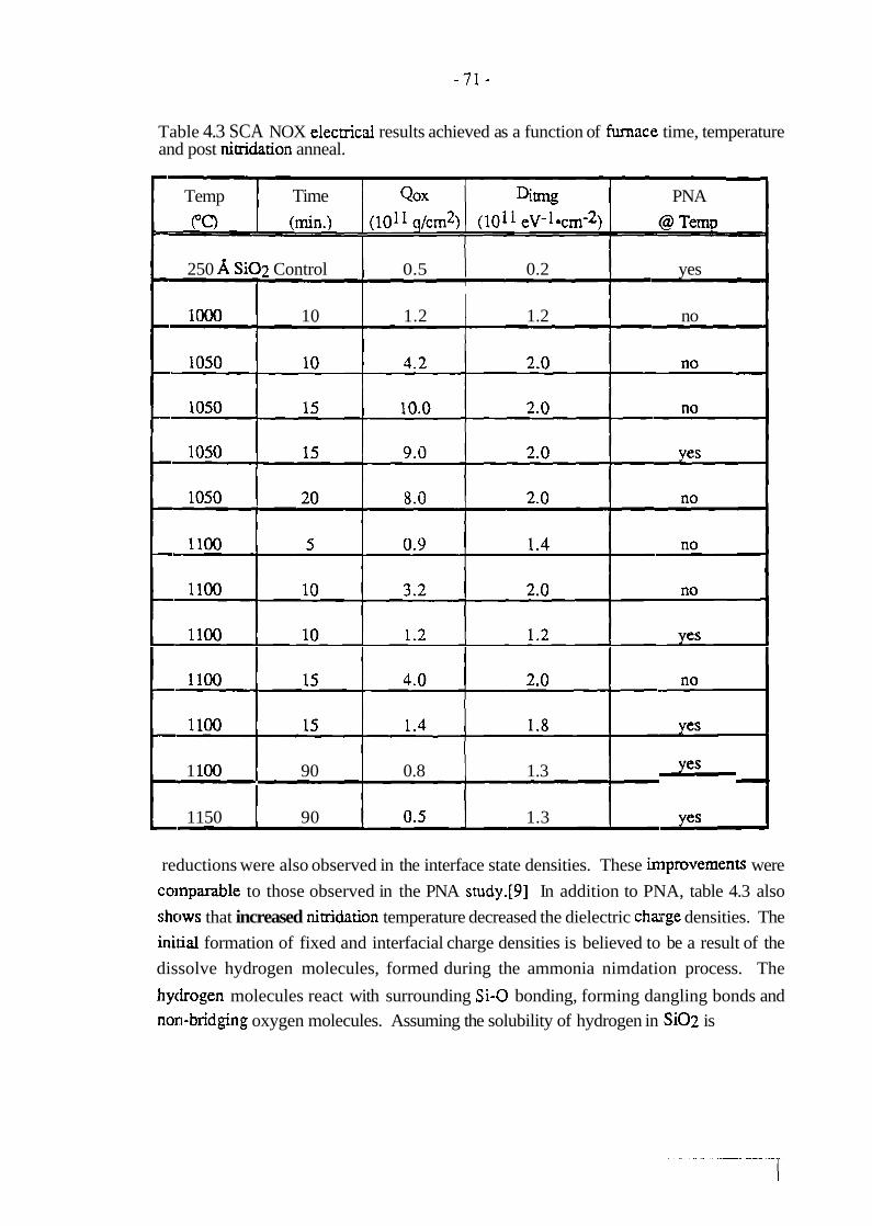
SCA NOX electrical results achieved as a function of furnace time, ............................................... temperature and post nitridation anneal .7 1
Effects of nitridation time and temperature on the index of refraction of ......................................................................... NOX dielectrics .74
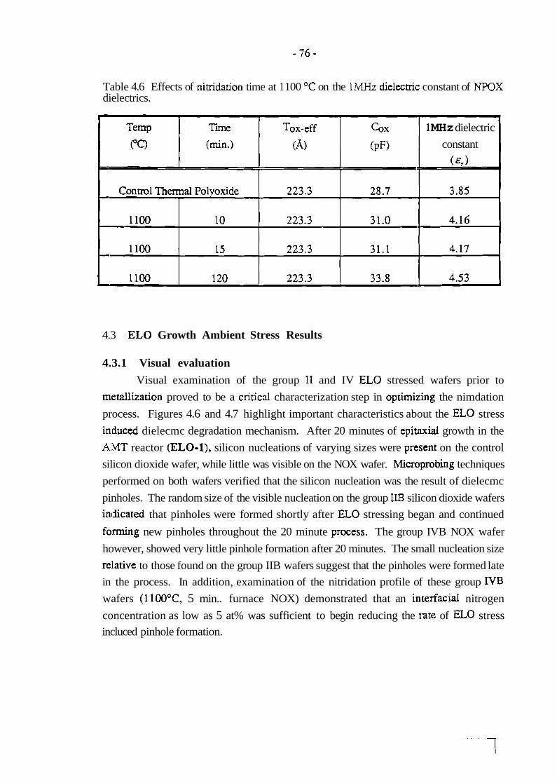
Effects of nitridation time at 1100 "C on the lMHz dielectric constant of ......................................................................... NOX dielectrics -74
Effects of nitridation time at 1100 "C on the lMHz dielectric constant of NPOX dielectrics ......................................................................... 76
Electrical breakdown results observed after 40 min. of ELO-2 growth ....................................................................... ambient stressing -8 1
Electrical tunneling results observed after 40 min. of ELO-2 growth ambient stressing .................................................................................. .8 1
Electrical breakdown results comparing ELO-1 process to ELO-2 ................. 83
.................. Electrical tunneling results comparing ELO- 1 process to ELO-2 .83
Electrical breakdown results comparing 10 min. and 60 min. 1100°C NPOX dielectrics after 40 min. EL0 stress ................................................... .88
Electrical tunneling results comparing 10 min. and 60 min. 1100°C NPOX dielectrics after 40 min. EL0 stress ................................................... .88
................. CV measurement results for NOX dielectrics nitrided at 1 100 "C .89
vii
LIST OF FIGURES
Figure Page
1.1 Comparison of die current vs . chip complexity for NMOS and CMOS .............................................................................. technologies -2
....................................................... 1 . 2 Scaling of MOSFET dimensions 3
...................................... 1.3 Cross-sectional view of a 3-D BiCMOS device 4
...................................................... 2.1 Three dimensional CMOS device 8
................................. 2.10 FIB photograph of a typical epitaxial nucleation site 15
........................... 2.1 1 FIB cross-section of the nucleation site from figure 2.10 15
2.12 SEM photograph highlighting crystal growth planes of typical nucleation ....................................................................................... sites -17
.................... 2.13 SEM photograph of thermal silicon dioxide dielectric pinholes 17
2.14 SEM photograph of a thermal silicon dioxide dielectric pinhole with the .................................................................. residual silicon nodule -18
...................................... 2.15 FIB cross-section of an epitaxial nucleation site 18
viii
2.16 Thickness of thermally grown nitride on (100) Si vs . nitridation time and temperature ............................................................................... -23
2.17 Change in free energy for several nitridation reactions .............................. 26
. .......................... 2.18 Typical nitrogen accumulation profile vs nitridation time 26
. ......................... 2.19 Typical hydrogen accumulation profile vs nitridation time 27
. 2.20 Typical nitrogen accumulation profile vs reoxidation time ......................... 27
2.2 1 Nitrogen concentration near the Si-Si02 interface vs . nitridation time and temperature ............................................................................... -30
.................. 2.22 Hydrogen concentration versus nitridation time and temperature 30
2.23 (a) AVm and (b) ADitm induced by 0.1 ~ l c r n 2 electron injection versus nitridation time and temperature ........................................................ 31
................. 2.24 Hydrogen concentration versus reoxidation time and temperature 33
2.25 Nitrogen Auger depth profiles for the initial oxynitride and the resulting ...................................................... effects of reoxidation temperature 33
2.26 (a) ADitm and (b) AVm induced by 0.1 ~ l c m 2 electron injection vs . ....................................................... reoxidation time and temperature 34
............. 2.27 Electron and hole mobility as a function of the effective electric field 35
.................................................................. 3.1 Polyoxide test structure 44
............... 3.2 PH3 doped amorphous silicon after 250 8, oxidation was removed 45
3.3 Phosphorus implanted amorphous silicon after 250 8, oxidation was ................................................................................... removed 45
............................................................ 3.4 Silicon dioxide test structure 47
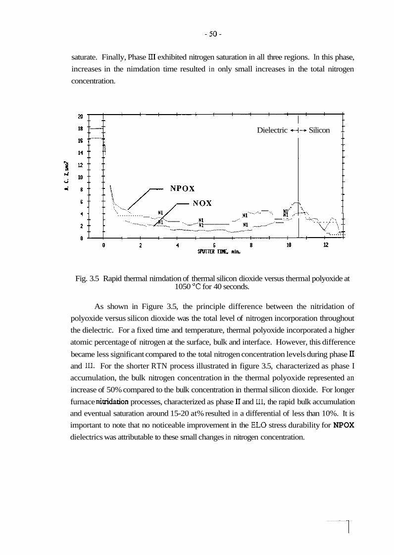
3.5 Rapid thermal nitridation of thermal silicon dioxide versus thermal polyoxide at 1050 "C for 40 seconds .................................................. 50
................. 3.6 Rapid thermal nitridation of polyoxide at 1050 "C for 40 seconds 51
. ...... 3.7 1100 "C furnace nitridation of silicon dioxide at 5. 10 and 15 min intervals 53
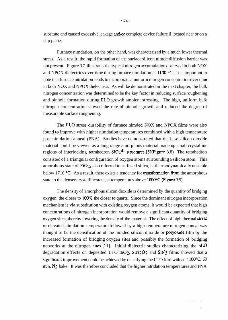
3.8 Model depicting the typical amorphous fused silica bonding structure ............ 53
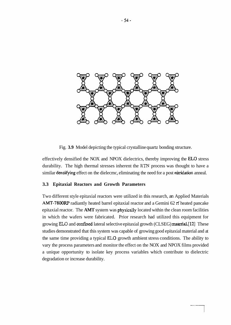
3.9 Model depicting the typical crystalline quartz bonding structure .................... 54
3.10 The effect of reoxidation on the nitrogen concentration in a 250 A NOX .................................................................................. dielectric -57
3.12 Example of sporadic surface nucleation on a 250 A NPOX dielectric . . . . . . . . . . . . .59
3.13 250 A NPOX dielectric after 0 2 plasma reoxidation ................................. 59
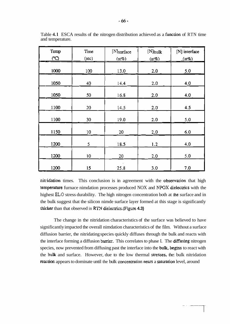
4.1 Average nitrogen content as a function of nitridation time for various thicknesses of thermal silicon dioxide. Ammonia nitridation conducted at 1150°C ..................................................................................... 64
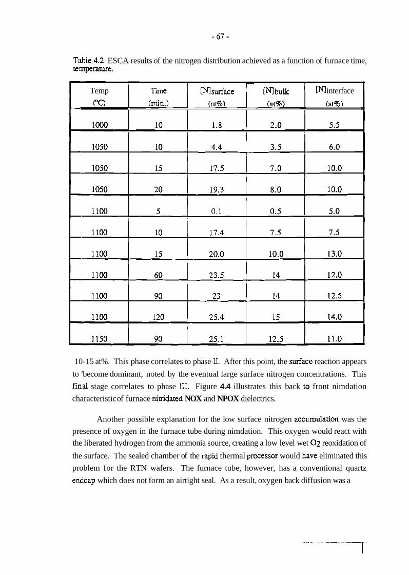
4.2 Example of the high surface nitrogen concentration observed in RTN NOX and NPOX dielectrics. The line indicates the dielectric/silicon interface . . . . . . . . . .68
4.3 Example of the high surface and bulk nitrogen concentration observed in high temperature furnace NOX and NPOX dielectrics. The line indicates the dielectric/silicon interface . . . . . . . . . . . . . . . . . . . . . . . . . . . . . . . . . . . . . . . . . . . . . . . . . . . . . . . . . . .68
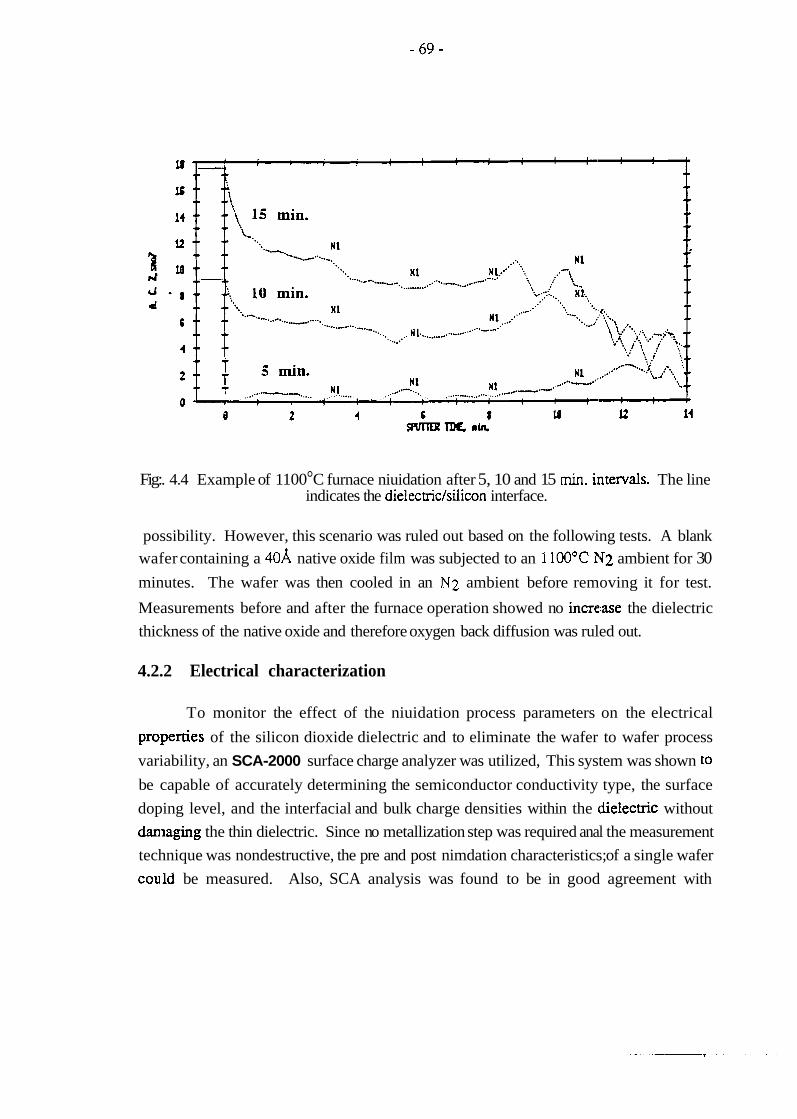
4.4 Example of 1100°C furnace nitridation after 5, 10 and 15 min. intervals. The line indicates the dielectric/silicon interface . . . . . . . . . . . . . . . . . . . . . . . . . . . . . . . . . . . . . .69
4.5 Effect of a 1000 "C N2 post nitridation anneal on the surface, bulk and interfacial nitrogen concentration with increasing nitridation time .. ................ 72
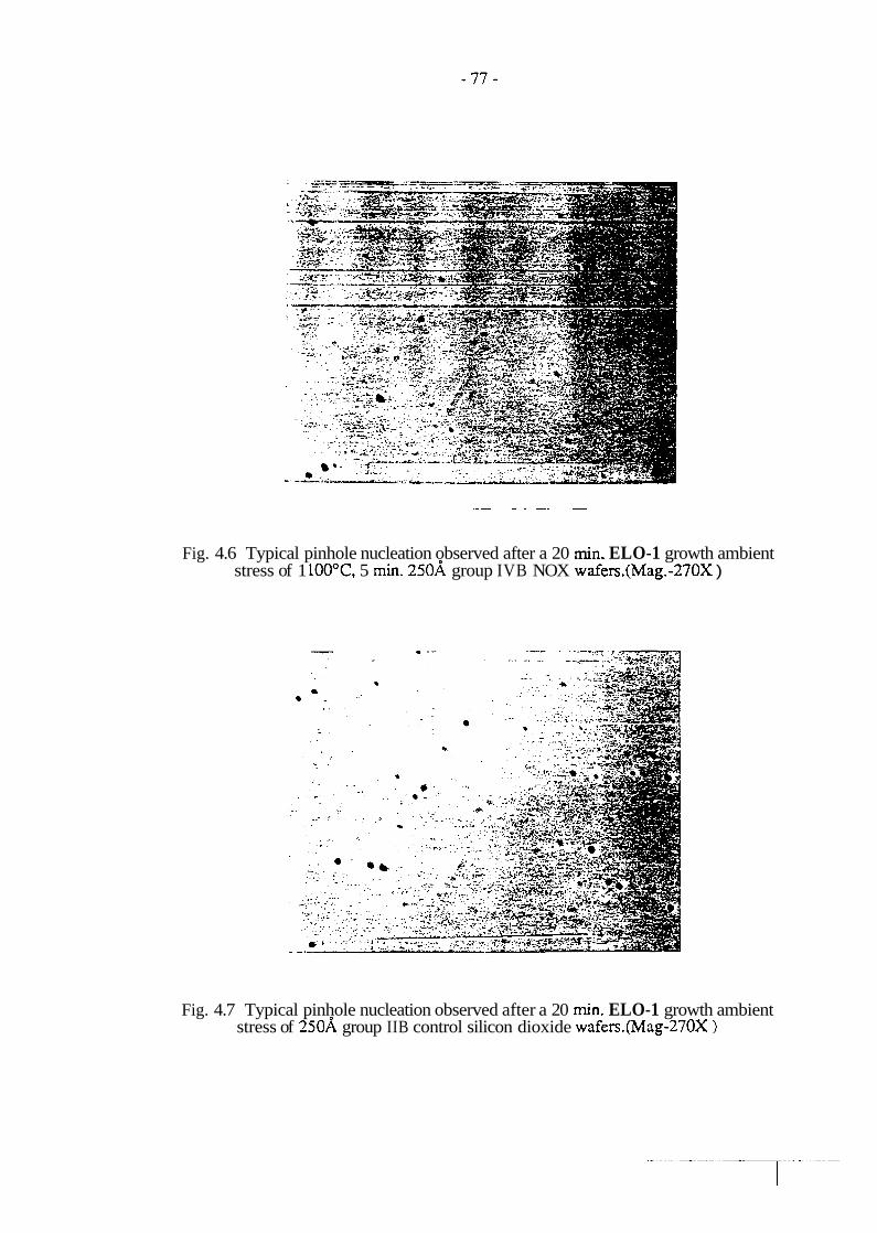
4.6 Typical pinhole nucleation ob2erved after a 20 min. ELO-1 growth ambient stress of 1 100°C, 5 min. 250A group IVB NOX wafers.(Mag.-270X ) . . . . . . . . . .77
4.7 Typical pinhqle nucleation observed after a 20 min. ELO-1 growth ambient stress of 250A group IIl3 control silicon dioxide wafers.(Mag-270X ) . . . . . . . . . . .77
4.8 Typical pinhole nucleation observed after a 40 min. ELO-1 growth ambient stress of 1 100°C, 5 min. group IVB NOX wafers.(Mag-270X ) . . . . . . . . . . . . . . . . .78
4.9 Typical pinhole nucleation observed after a 40 min. ELO-1 growth ambient stress of group IIl3 control silicon dioxide wafers.(Mag-270X ) . . . . . . . . . . . . . . . . . .78
4.10 Distribution of thermal polyoxide and NPOX dielectric breakdown fields before and after 40 minutes of EL0 stressing . . . . . . . . . . . . . . . . . . . . . . . . . . . . . . . . . . . . . . . .8 1
4.11 Distribution of NPOX dielectric breakdown fields after 40 min. EL0 ambient stressing in the AMT (ELO- 1) and Gemini (ELO-2) systems . . . . . . . . . . . .83
4.12 Change in electric field characteristics in an 1 100°C, 10 min. NPOX dielectric before and after stressing . . . . . . . . . . . . . . . . . . . . . . . . . . . . . . . . . . . . . . . . . . . . . . . . . . . .84
4.15 Current density versus electric field for 1100 "C, 10 min. NPOX control after 40 min. EL0 stress. (positive sweep) .......................................... .86
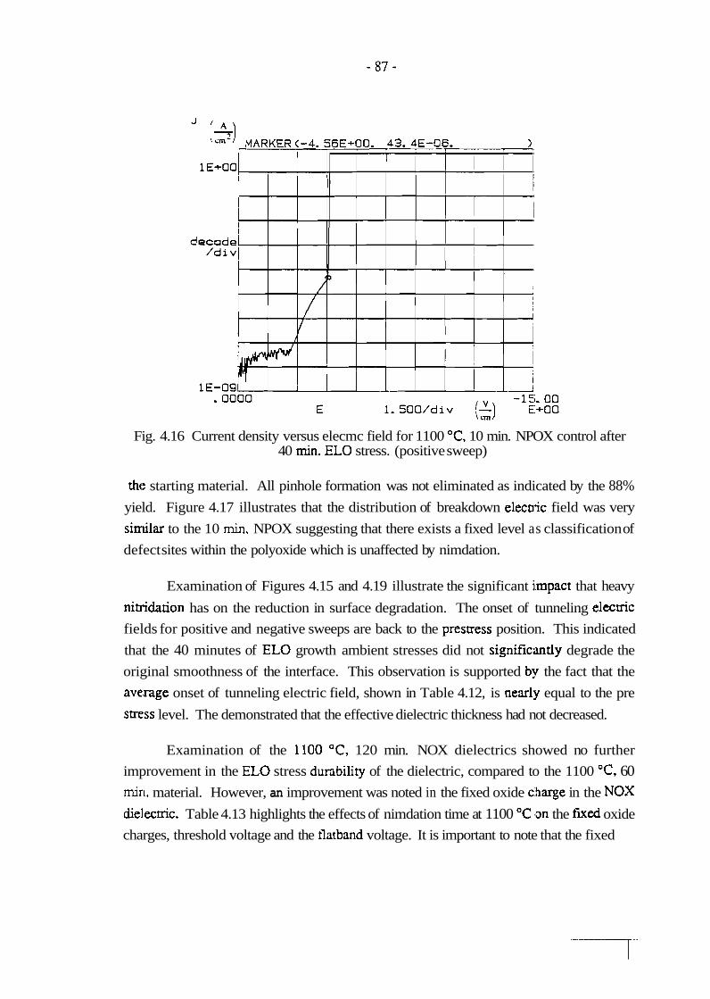
4.16 Current density versus electric field for 1100 "C, 10 min. NPOX control .......................................... after 40 rnin. EL0 stress. (positive sweep) .87
4.17 Distribution of 10 min. and 60 rnin. NPOX dielectric breakdown fields after ........................................................ 40 rnin. of EL0 ambient stress .88
4.18 Current density versus electric field for 1100 "C, 60 rnin. NPOX control .......................................... after 40 min. EL0 stress. (positive sweep) .9 1
4.19 Current density versus electric field for 1 100 "C, 60 min. NPOX control after 40 min. E L 0 stress. (negative sweep) ........................................... 91
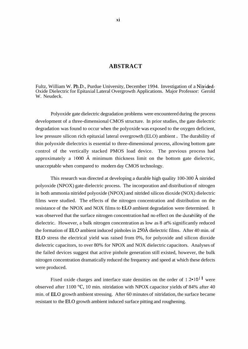
ABSTRACT
Fultz, William W. Ph.D., Purdue University, December 1994. Investigation of a Nitrided- Oxide Dielectric for Epitaxial Lateral Overgrowth Applications. Major Professor: Gerold W. Neudeck.
Polyoxide gate dielectric degradation problems were encountered during the process
development of a three-dimensional CMOS structure. In prior studies, the gate dielectric
degradation was found to occur when the polyoxide was exposed to the oxygen deficient,
low pressure silicon rich epitaxial lateral overgrowth (ELO) ambient . The durability of
thin polyoxide dielectrics is essential to three-dimensional process, allowing bottom gate
control of the vertically stacked PMOS load device. The previous process had
approximately a 1000 A minimum thickness limit on the bottom gate dielectric,
unacceptable when compared to modern day CMOS technology.
This research was directed at developing a durable high quality 100-300 A nitrided
polyoxide (NPOX) gate dielectric process. The incorporation and distribution of nitrogen
in both ammonia nitrided polyoxide (NPOX) and nitrided silicon dioxide (NOX) dielectric
films were studied. The effects of the nitrogen concentration and distribution on the
resistance of the NPOX and NOX films to EL0 ambient degradation were tletermined. It
was observed that the surface nitrogen concentration had no effect on the durability of the
dielectric. However, a bulk nitrogen concentration as low as 8 at% significantly reduced
the formation of EL0 ambient induced pinholes in 250A dielectric films. After 40 min. of
EL0 stress the electrical yield was raised from 0%, for polyoxide and silicon dioxide
dielectric capacitors, to over 80% for NPOX and NOX dielectric capacitors. Analyses of
the failed devices suggest that active pinhole generation still existed, however, the bulk
nitrogen concentration dramatically reduced the frequency and speed at which these defects
were produced.
Fixed oxide charges and interface state densities on the order of 1 .2*101 1 were
observed after 1100 "C, 10 min. nitridation with NPOX capacitor yields of' 84% after 40
min. of EL0 growth ambient stressing. After 60 minutes of nitridation, the surface became
resistant to the EL0 growth ambient induced surface pitting and roughening.
CHAPTER 1: INTRODUCTION
1.1 Background
The theory of the surface field effect transistor was first proposed by Lilienfeld in
the late 1920's followed by Heil in the early 1930's. However, it took until the late 1940's
before the theory was first demonstrated by Schockley and Pearson. These field effect
devices used thin sheets (approx. 20 pm thick) of mylar or mica as the dielectric spacer
between the metal gate electrode and the semiconductor.
In 1960, Kahng and Atalla fabricated the first planar MOSFET structures utilizing
silicon dioxide grown in high pressure steam. In 1963, the Grove, Deal and Snow refined
this structure and the fabrication process, developing the first commercially usable planar
MOSFET process. The critical factor in making this process commercially viable, was the
development of an electrically stable silicon dioxide dielectric. In that same year, Wanlass
and Sah proposed the pairing of p-channel (PMOS) and nchannel (NMOS) transistors and
patented the first complementary metal oxide semiconductor (CMOS) structure.
The first CMOS integrated circuits were fabricated in 1966. Due to the relatively
slow speed, the significantly higher fabrication cost, the increased susceptibility to latch-
up, and the lower packing densities of CMOS compared to PMOS and later to NMOS,
CMOS ICs were limited to specialized applications requiring low power applications.
However, with the power dissipation and density limitations presented by silicon and the
packaging technology, combined with circuit integration which was quadrupling every
three years, it became apparent that NMOS circuits would not be able to meet future needs.
Figure 1.1 shows the dramatic difference in power consumption versus chip complexity
between CMOS and NMOS. By the late 1970's, technology and process advancements
Fig. 1.1 Comparison of die current vs. chip complexity for NMOS and CMOS technologies. [l]
had made CMOS comparable to NMOS in speed and by 1980, CMOS had become the
dominant technology for large scale integrated circuits.
Since the early 1960's. the average rate of scaling has been approximately 13% per
year.(Figure 1.2) By 1989 CMOS integration had exceeded 1 million transistors a die in
non-repetitive circuit designs such as microprocessors. At this rate 0.2 pm geometries will
be realized in the year 2000, allowing circuit integration which incorporates hundreds of
millions of transistors. However, according to simulations of conventional planar
technology devices, the physical geometric limit was estimated at 0.25 pm In addition, the
speed enhancement associated with the scaling of conventional planar technology devices
below 1 pm have experienced diminished returns. At these geometries, the inmnsic
parasitic capacitances inherent in the planar technology become the limiting factor in device performance.
To overcome these problems, a great deal of developmental research has been directed at new process technologies and new device structures. The development of
silicon on insulator (SOI) devices and three dimensional strucrures are products of this
research. The resent development of a selective epitaxial growth (SEG) silicon bipolar
A
200 - NMOS
A
s -
100 2 00 300
Chip complexily (%I
Fig. 1.2 Scaling of MOSFET dimensions. [2]
technology has pushed silicon technology into applications which were once attainable only
with gallium arsenide devices. Due to increased speed, latch-up immunity and radiation
hardness observed with SO1 CMOS devices, similar expectations exist for advanced
CMOS applications.
The goal of this research was to assist in the overall development of a three
dimensional BiCMOS process.(Figure 1.3) The structure incorporates many novel
concepts which suggest performance advantages unattainable by convention planar
BiCMOS processes. One of these concepts was the development of a vemcally stacked,
dual gated, fully depleted PMOS load device. The dual gate feature produces twice the
channel conductance of a conventional PMOS device, thereby allowing the device geometry
to be reduced by a factor of two for higher levels of integration. In addition, the use of
epitaxial lateral overgrowth (ELO) allowed the PMOS load characteristics to be optimized
independent of the NMOS driver, and the NPN bipolar junction transistor characteristics to
be optimized independent of the CMOS. The vertical stacking has also shown to eliminate
the latch-up paths which have plagued the planar CMOS process since it's inception.
Dual Gate I Poly Emitter
Collector Contact
I p substrate I
Oxide Poly Metal
Fig. 1.3 Cross-sectional view of a 3-D BiCMOS device. [3]
Although conceptually developed, several key processing problems still remain to
be solved. This research addressed the specific problem of silicon dioxide degradation
resulting from exposure to the low pressure, high temperature ambient during EL0 growth.
This degradation resulted in a process limit of about 1000 A on the thickness of the bottom
gate dielecmc of the PMOS load device, a limit which threatens the future viability of the
structure; or at least the efficiency of the bottom channel of the PMOS load.
1.2 References
[I.] High-Speed Semiconducror Devices, edited by S.M. Sze, Wiey-Interscience Publication, John Wiley & Sons, Inc., 1990.
[2] S. Wolf, Silicon Processing For The VLTI Era, Volume 2: Process Integrarion, Lattice Press, 1990.
[3] R. Bashi., S. Venkatensan, G.W. Neudeck, and J.P. Denton, "A Polysilicon Contacted Subcollector BJT for a Three-Dimensional BiCMOS Process," IEEE Eiecnon Device Lerrers, vol. 13, no. 8, pp. 392-395, August 1992.
CHAPTER 2: LITERATURE REVIEW
2.1 Problem Statement
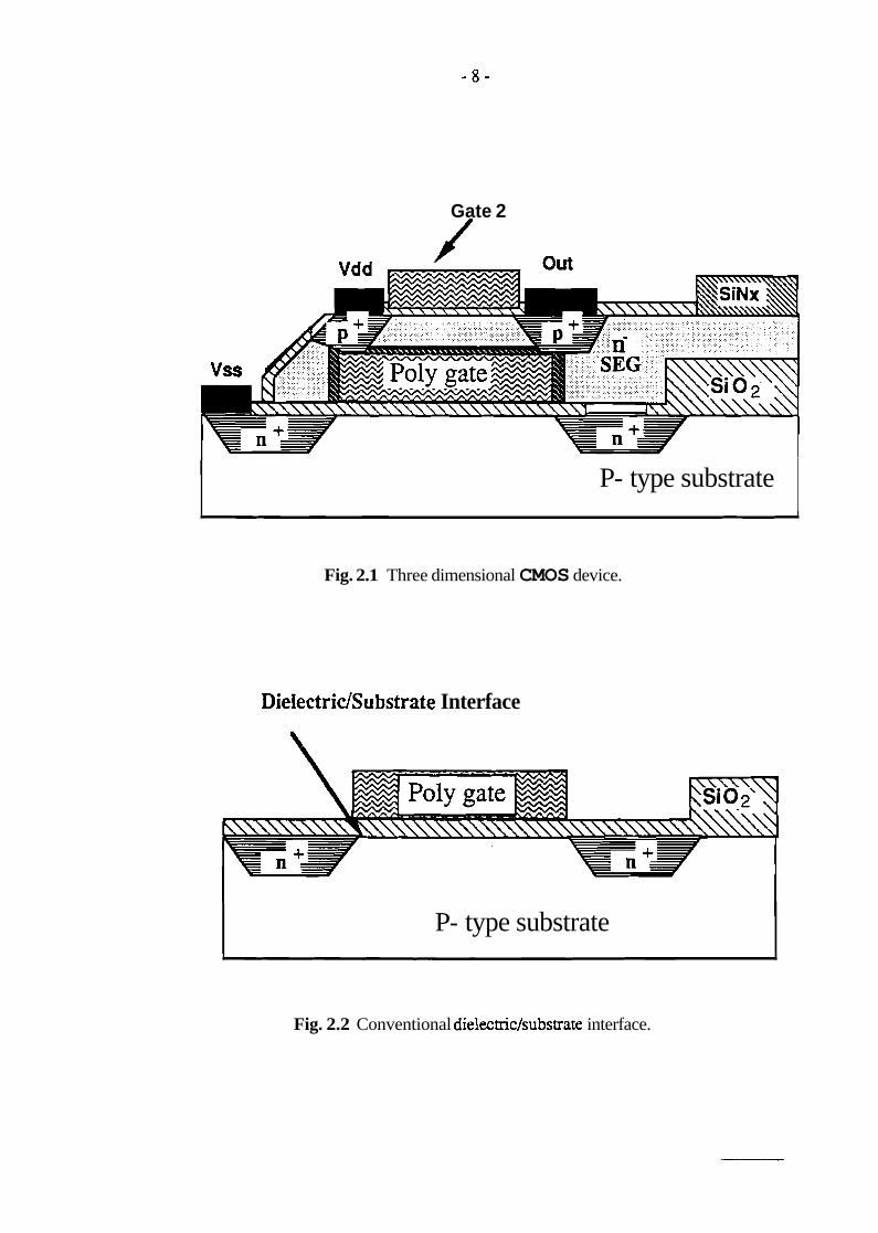
The original three-dimensional CMOS inverter structure, first developed in 1989 [I], utilized epitaxial lateral overgrowth (ELO) to vertically stack a PMOS load device over
a standard substrate NMOS dnver.(Figure 2.1) A novel component of' this structure was
the utilization of a shared gate. This was implemented by oxidizing the polysilicon gate
conductor of the NMOS driver prior to EL0 growth.(Figure 2.3) This polyoxide became
the gate dielectric for the PMOS load. Later refinements of the 3-D structure resulted in the
addition of a second topside polysilicon gate on the PMOS load device. Typically p-
channel transconductance is about half that of an n-channel device, for a given geometry.
This arrangement made the total PMOS msconductance of the dual gated load comparable
to that of the NMOS driver, thereby allowing the total footprint of the CMOS inverter to be
controlled by the NMOS driver.
It is important to note that the bottom gate/dielectric/substrate structure of the PMOS
load device was constructed in reverse order, compared to conventional MOS processes.
With conventional MOS devices, the growth of the gate dielectric from the substrate
concurrently forms the dielecmc/substrate interface. Therefore, the electrical properties of
the interface are dominated by the dielectric growth kinetics.(Figure 2.2) To date, dielectric
research has concentrated on process development targeted at optimizing the electrical
characteristics of this interface. With the novel PMOS structure, the gate dielectric was
grown from the polysilicon gate material. However, the dielecmc/substrate interface
occurs at the surface of this grown dielecmc and is formed during epitaxial lateral
overgrowth.(Figure 2.4) Therefore, the electrical properties of the bottom gate
Fig. 2.3 Gate oxide formation for the bottom gate of the PMOS load device.
DielectricISubstrate Interface
P- type substrate
Fig. 2.4 Dielectric/substrate interface for stacked PMOS load device.
dielectric/ELO substrate interface are controlled by the epitaxial growth kinetics and the
material characteristics of the top surface of the gate dielecmc. The novel device structure
combined with the unique dielecmcfmterface formation has created an opportunity for new
and innovative gate dielecmc research
Early in the development of the 3-D CMOS strucrure it was discovered that thin
silicon dioxide films, such as the bottom gate dielectric of the PMOS load, were severely
degxaded in the low pressure ambient during EL0 growth.[2] This degradation placed a
process limit of about 1000 A on all oxide dielectrics exposed to the EL0 ambient. With
conventional CMOS technology utilizing gate dielecmc thicknesses less than 200 A, the
degradation problem jeopardized the enhance performance of the structure.
Initial investigation of the problem highlighted several critical factors controlling the degradation of silicon dioxide in the EL0 ambient. In Si-SiO2 systems, degradation can
occur through the dispropomonation reaction
given sufficiently low partial pressures of 0 2 or H20 at the reaction site. This reaction is a
strong function of pressure, temperature, silicon concentration, and mobility of the volatile
species. In several studies conducted by Hofmann er a1.[3,4], it was found that several of
conditions were achieved during post-oxidation annealing (POA) of thermally grown
silicon dioxide films. The low partial pressure of oxygen or water in conjunction with the
enhanced diffusion of Si and SiO at defect sites in the 500 A silicon dioxide films created
pinholes in the dielectrics. These same conditions and worse exist in the epitaxial reactor
with the addition of a large Si source, as well as low pressure.
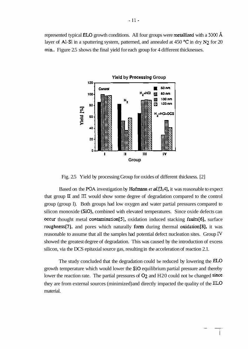
To quantify the amount of degradation, four groups of test wafers containing MOS
capacitor structures were prepared.[2] The thermally grown silicon dioxide dielectric
thickness ranged from 600 to 1200 A. Group I was the control group experiencing no epitaxial reactor stress. Group I1 was subjected to a 5 minute H2 bake at 900 OC at
atmospheric pressure followed by 20 minutes at 950 OC at 150 Tom. Group III was
identical to the second group, with the exception that HCL was introduced in addition to H2 during the 20 min. bake. The HCL partial pressure was 3 Torr. Group IV was the
same as the third group, with the exception that H2, HCL and SiC12H2 (DCS), each with a
partial pressure of 1 Torr, were introduced during the 20 min. bake. The fourth group
represented typical EL0 growth conditions. All four groups were metallized with a 3000 A layer of A1-Si in a sputtering system, patterned, and annealed at 450 OC in dry N2 for 20
min.. Figure 2.5 shows the final yield for each group for 4 different thicknesses.
Yield by Processfng Group
- I I I 111 I V
Group
Fig. 2.5 Yield by processing Group for oxides of different thickness. [2]
Based on the POA investigation by Hofmann er aI.[3,4], it was reasonable to expect that group I1 and III would show some degree of degradation compared to the control
group (group I). Both groups had low oxygen and water partial pressures compared to
silicon monoxide (SiO), combined with elevated temperatures. Since oxide defects can
occur thought metal contamination[5], oxidation induced stacking faults[6], surface
roughness[7], and pores which naturally form during thermal oxidation[8], it was
reasonable to assume that all the samples had potential defect nucleation sites. Group TV showed the greatest degree of degradation. This was caused by the introduction of excess
silicon, via the DCS epitaxial source gas, resulting in the acceleration of reaction 2.1.
The study concluded that the degradation could be reduced by lowering the EL0 growth temperature which would lower the SiO equilibrium partial pressure and thereby lower the reaction rate. The partial pressures of 0 2 and H20 could not be changed since
they are from external sources (minimized) and directly impacted the quality of the EL0
material.
Another option not addressed in the original study was the use of nitrogen to
change the chemical composition of the silicon dioxide material by increasing the material
bond strength[9] and lowering the defect density[lO]. The increase in bond strength would
increase the activation energy required to form volatile SiO species. Lowering the defect
density would limit the number of potential reaction sites for dielecmc degradation. In
addition, the resistance of nimdes and oxynimde to diffusing material would further reduce
the mobility of the SiO species that does form. The net result should be a more resilient
dielecmc material to the epitaxial growth ambient
In a later study, LPCVD silicon nitride/thermal silicon dioxide stacks (group Il and
an oxynimde composition (group II) were compared against thermal silicon dioxide (group
and thermal polyoxide (group IV). Again capacitor structures were utilized to evaluate
the degree of dielecmc degradation. The dielectric thicknesses ranged from about 225 A to 1425 A, except for the LPCVD Si3N&.hermal Si02 stacks which were 100 A thicker due
to the nimde deposition. Each dielecmc material type and thickness were divided into a
control group and a selective epitaxial growth (SEG) ambient stress group. All stress groups were subjected to a 5 minute bake in H2 at 970 OC at 150 Torr, 30 seconds in H2
and HCL at the same temperature and pressure, followed by a 10 minute exposure H2,
HCL and DCS at the same temperature but at a reduce pressure of 40 Torr.[11]
The study results correlated with the original findings, the severity of dielectric
degradation in group I11 and group IV increased dramatically as the dielectric thickness
decreased below 1000 A. However, the group I and group II nimde dielectrics exhibited
significantly less degradation with group I exhibiting the least.(Figures 2.6-2.9)
Failure analysis was performed on a large sample of the shorted silicon dioxide
dielectrics from group 111. Using mechanical microprobing techniques, specific areas of
the dielecmc were verified as shorted and marked for further analysis. Many of these
designated-sites were covered by silicon nodules with growth planes along the [100],
['I 101, and ['I1 11 direction. Figure 2.10 shows a typical example of the observed silicon
nodule. This particular nodule was located under a metal capacitor pad with the center of
the nodule protruding from under the metal. The mangular facets forming the crest of the
nodule are (1 11) growth planes. Figure 2.1 1 shows the vertical cross-section, performed by Focused Ion Beam (FIB) milling, of the nodule shown in Figure 2.10. From this
vertical prospective, the (100) and (110) growth planes become visible. The crystal
orientation of the growth planes was a clear indication that the silicon nodule was a result of
Fig. 2.10 FIB photograph of a typical epitaxial nucleation site.
Fig. 2.1 1 FIB cross-section of the nucleation site from figure 2.10.
selective epitaxial growth (SEG) from (100) silicon. The seed window to the underlying
(100) silicon was speculated to be the result of silicon dioxide deterioration at an oxide
defect site.
Once the defect sites were verified and marked, the wafers were subdivided into
two groups. The first group was selectively etched using a combination of Sirtl etch (400ml H20 : 400x111 HF : 200gm CrO3) and Silicon etch (50:3: 1 HN03:CH3COOH:HF').
The crystal etch selectivity of the Sirtl etch was used to cleave the nodules into smaller particles. The high Si:Si02 etch selectivity was used to then dissolve these smaller
particles leaving the underlying oxide intact. Field Emission Microscopy (FEM) examination of the partially etched silicon nodules provided further evidence of the crystal
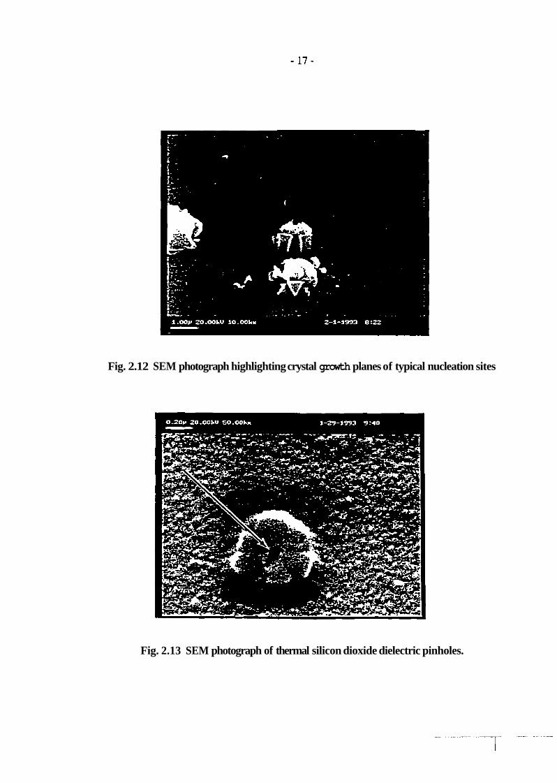
oriented growth planes of the silicon nodules.(Figure 2.12) FEM examination of
completely etched silicon nodules revealed pinholes in the silicon dioxide dielectric, located
at the center of the nucleation sites.(Figures 2.13 and 2.14) The pinhole diameters on the
order of 200 A were measured using a particle measurement system, a feature of the FE
microscope. It is believed that all of the nucleation sites resulted from dielectric pinholes
induced by the epitaxial growth ambient However, some pinholes were believed to be too
small to be resolved at 200,000 times magnification. Although higher magnification was
possible using the FE microscope, the electron beam became so concentrated that it
liquefied the silicon dioxide and filled in the pinhole.
The second group was cross-sectioned and visually examined, using FIB milling
and microscopy techniques, in order to evaluate the uniformity and extent of degradation of
the underlying silicon dioxide dielectric. Attempts were also made to cross-section and
visually examine the dielecmc pinhole, but proved to be beyond h e capability of the
machine. Figure 2.15 indicates a typical example of a FIB cross-section. No noticeable
roughening or thinning of the silicon dioxide dielectric was observed along the entire span
of the nodule. This observation combined with the FE microscopy analysis added
considerable support to the theory that silicon dioxide defects were the focal point of the
dielectric degradation. These photographs represent the first conclusive visual evidence
that the epitaxial ambient induced dielectric degradation does not roughen and thin the
overall dielecmc but rather is highly site specific. This highly localized silicon dioxide
deterioration agreed with the POA studies by Hoffman er d..[3,4]
Fig. 2.12 SEM photograph highlighting crystal growth planes of typical nucleation sites
Fig. 2.13 SEM photograph of thermal silicon dioxide dielectric pinholes.
Fig. 2.14 SEM photograph of a thermal silicon dioxide dielectric pinhole with the residual silicon nodule.
?
Si Nodul
S i Sub
Fig. 2.15 FIE3 cross-section of an epitaxial nucleation site.
Although the group I and group I1 nitrided dielectrics look promising, several
questions still remained to be answered. To date, only epitaxial lateral growth over thermal
silicon dioxide has proven to form a high quality MOS interface, exhibiting both low
trapped charge and surface state densities. The exact chemical bonding mechanism which
occurs, between the growing EL0 front and the gate dielectric, is not currently understood.
Therefore, it cannot be predicted what effect the silicon nitride or oxynitride surface will
have on the quality of the MOS interface.
Assuming that a conventional interface forms between the oxynimded dielectric and
the ELO, the question remains whether nimded dielectrics are reliable and stable enough to
be utilized as a gate dielecmc. It is immediately apparent that the group I material would be
unsuitable for conventional MOS applications. However, nimde/oxide stack dielecmc has
been used in electrically erasable programmable read only memories (EEPROM) because of
its excellent charge trapping and storage characteristics at the nitride-oxide interface and in
the nitride bulk.[12,13,14] This charge trapping characteristic however, is catastrophic for
conventional MOS applications. This leaves the group II material, the oxynimde or some
form of nimded oxide, as the most plausible solution.
2.2 Gate Dielectric Review
2.2.1 Introduction
Since the late 1980's, the drive to "up integrate" more feanues and functions onto a
single die has pushed circuit integration from very large integrated circuit (VLSI) to ultra
larger integrated circuit (ULSI) processing. This up integration is accomplished by scaling
device geomemes into the sub micron region. Scaling rules mandate that MOS device
geometries of a micron or less require gate dielecmc thickness of 200 A or less. At this
thickness problems such as, high field dielecmc breakdown and hot carrier stress induced
dielecmc degradation, become critical.[l5] For larger geometries these were considered
negligible second order effects. These problems and the drive to develop ULSI processing
have sparked renewed interest in gate dielectric research. New dielecmc materials are being
developed and evaluated such as nitrides, oxynimdes, fluorinated silicon dioxides[l6,171
and CVD oxide/thermal oxide stacks.[l8,19] In addition, new information about thermal
silicon dioxide is being discovered. The remainder of this chapter will be devoted to
reviewing the current research on thermal silicon dioxide dielecmcs, followed by a detailed
review of oxynimde dielecmcs.
2.2.2 Silicon dioxide update
In developing an 80 A silicon dioxide gate dielectric for ULS:I applications, S.L.
Wu et al. [20] developed a process which embodies a significant portion of the current
knowledge of silicon dioxide growth and defect formation. Silicon dioxide dielecmcs
prepared by this process showed very high dielecmc breakdown fields in excess of 16
MVIcm, very low interface state densities of 3 109 lev-cm2 at midgap and 30 times
smaller dielecmc leakage currents than conventional thermal silicon dioxides, translating
into an order of magnitude longer predicted lifetime. Because of the superior results, the
process flow was utilized as an outline for introducing the state-of-the-art in silicon dioxide
processing.
The process began with a RCA clean. This two stage cleaning process consisted of
a hot water-diluted hydrogen peroxide and ammonium hydroxide bath to remove organics
and particulates, followed by a hot water-diluted hydrogen peroxide and hydrochloric acid
bath to remove Al, Fe, Mg, and other metallic contaminants.[21] Effective chemical wafer
cleaning has been shown to improve the quality of thermal silicon dioxide dielecmcs by
reducing the formation of oxidation induced stacking faults [22], by increasing the inmnsic
dielectric breakdown characteristics through the reduction in surface-microroughness,[7]
and by reducing the defect density related to oxidized metal contarnination incorporated into
the silicon dioxide structure.[5] In addition to the dielectric degradation, the microroughness of the Si02/Si surface also has a degrading effect on carrier mobility.
MOSFET transconductance, and carrier transfer efficiency.[20,23,24] ,Although the RCA
cleaning process has become an industry standard, refinements are continually being made
to reduce the amount of surface microroughening. In addition, surfactants are being
incorporated to enhance the removal of particulate contamination.
The second step of the oxide process incorporated an aqueous solution of HF to
remove the native oxide. This step was also designed to passivate the silicon surface
inhibiting native oxide regrowth. T. Ohmi et al. [25] demonstrated that significant
improvements in silicon dioxide reliability were achieved by removing that native oxide and
subsequently passivating the surface with hydrogen and fluorine.[7,25,26,27] The
demonstrated that the combination of oxygen and water (or moisture), at room temperature,
was all that was required to grow a native oxide several angstroms thick. E.T. Paul et al.
[28] stated that a thin 5-30 %i layer of native oxide seriously degrades the quality of the
thermally grown silicon dioxide.
It was also demonstrated by M. Hirose er al. [26] that the addition of a small
amount of Si-F bonds within a hydrogen passivated silicon surface creates a synergistic
relationship. The charge transfer in the vicinity of the fluorine atom enhanced the strength
of the chemical bonds between Si and H atoms. This condition hindered the regrowth of
the native oxide prior to oxidation. In addition, the bonding structure created atomic layer-
by-layer oxidation growth planes parallel to the surface, promoting better dielectric
uniformity.[25,26] Silicon dioxide dielectrics grown from HF passivated surfaces
exhibited lower dielectric leakage and improved projected lifetirnes.[27]
The next step in the process involved a 600 OC nitrogen preoxidation anneal. The
study reported that the nimded silicon surface exhibited many advantageous characteristics.
The Si-N bonding resulted in a reduced stress interface after oxidation. In addition, the
nitrogen banier slowed down the diffusion of the oxidizing species creating longer, more
controllable oxidation schedules. However, unlike the oxynimdes discussed in the next
section, x-ray photoemission spectroscopy (XPS) analysis did not detect any nitrogen in
the silicon dioxide at the end of the process flow.
The HF surface strip and passivation combined with the preoxidation nitrogen
anneal were concluded to be the key steps in producing the crystalline-like oxide layer at the Si02/Si interface. This crystalline-like interface resulted in a significant reduction in
surface microroughness and also produced a low stress interface, compared to conventional
silicon dioxides.
The final steps, dry 0 2 oxidation and post oxidation anneal (POA) in N2 concluded
the silicon dioxide dielectric process. Although this process produced excellent results
compared with conventional silicon dioxide processes, studies have shown that POA can
have detrimental effects on the electrical stability of the dielectric. Post oxidation anneals
can produce volatile SiO species, as noted in section 2.1. This instability has been shown to increase the intrinsic hot carrier traps and the surface state density at the SiOgSi
interface. This instability, however, can be easily removed by a subsequent 1 minute 0 2
anneal. [29,30]
Although the original process was designed for a 80 A film, it was felt that the
process could be expanded to 100-300 %, silicon dioxide dielectrics while retaining the
superior eIecmcal properties compared to conventional silicon dioxides. This process
provided the framework for developing the thermal silicon dioxide and polyoxide processes utilized in the research.
2.2.3 Oxynitride overview
Silicon nitrides have long been an attractive alternative for silicon dioxide dielectrics
in MOS applications. P. Fahey er al. [3 I.] showed that thermal silicon, nitride retards the
diffusion of boron and phosphorus impurities. This was attributed to the depletion of
interstitial during direct nitridation of the silicon. S. Mizuo er al. [32] and Y. Hayafuji er al. [33] demonstrated, in separate studies, that thermally grown silicon nitride inhibited the
formation of new stacking faults and reduced the quantity of existing faults. Both of these
characteristics are extremely beneficial for large scale integration.
Thermally grown silicon nitrides however, have many drawbacks which have
hindered their widespread application. As shown in Figure 2.16, nimdation growth
kinetics are extremely self limiting.[9] The high temperature and long growth times
overwhelm the thermal budgets of most VLSI processes. Although chemical vapor
deposition (CVD) helped overcome this thermal restriction, the electrical quality of the films are typically degraded.
Another key problem with silicon nimde is the high stress which forms at the Si3NdSi interface. This stress results in high interface trap and fixed charge densities.
The interface traps are typically donor-like and resuIt in a gate potential dependent variable
charge. The interface charge combined with the fixed charge create coulombic scattering
centers which severally degrade carrier mobility and MOS transconductance. In addition,
research has shown that normal operating conditions can result in the additional formation
of surface states by hot carrier injection.[9]
In the late seventies, T. Ito er al. 1351 and M . Nairnan er al. [36] first conceived that
idea of incorporating the beneficial qualities of silicon nimde with those of silicon dioxide.
They independently developed an atmospheric nimdation process utilizing an ammonia
source. The resulting nimded silicon dioxide, today referred to as oxynimde, was resistant
to interface state genexation under electrical stress, insensitive to xadiation, and provided a
NITRIDATION KINETICS I
Fig. 2.16 Thickness of thermally grown nitride on (100) Si vs. nimdation time and temperature. [9]
barrier to various dopants and contaminants. In addition, the frnal dielecmc thiclcness was
controlled by the initial silicon dioxide. These factors, combined with the moderate thermal
budget of the nitridation process, created a dielecmc process compatible with most VLSI
processes. However, the nitridation process introduced a large number of electron mps
both at the interface, in the form of surface states, and in the bulk, in the form of deep level
traps. In addition, the dielectric exhibited the characteristically high fixed positive charge
densities of silicon nitride.
Since its inception, extensive research has been directed at analyzing the nimdation
process variables and their impact on the quality of the final dielectric. The remainder of
this chapter will be devoted to defining those process variables and their effect on the
quality of the oxynitride dielecmc.
2.2.3.1 Kinetic model of oxynitride formation
B. Liu er a1.[36] postulated that four principle chemical reactions control the formation of silicon oxynitride (Si2N20). The possible reactions for the nimdation of
silicon dioxide using an ammonia source were:
To aid in the discussions on the kinetic reactions of nitridation, a multilayer model was developed. The oxynitride dielectric was divided into three regions, the surface, the bulk, and the interface. The principle reasoning behind this division was that each region consisted of a unique set of boundary conditions which caused one or more of the possible
reactions to dominate.
In the surface region, the lack of excess silicon, the direct contact with the nitriding
ambient, and easy removal of the by-products favor reaction 2.2. Reactions in this region
are reaction rate limited.
Moving from the surface into the bulk dielectric, two key changes occur. First, excess silicon becomes available in the form of interstitial and disrupted Si-0 bonds. During ammonia nimdation, hydrogen species in the form of HxO and Hx (where 1a<3) ,
diffuse into the silicon dioxide film. These species disrupt the Si-0 bonds throughout the bulk of the film, especially near the Si02/Si interface where these bonds are strained. This
excess silicon source allows reactions 2.3 and 2.4 to a become a contributing factor in the
nimdation process. The second change occurs because of the concomitant nitridation of the
surface. As the surface becomes more heavily nimded, it becomes a greater barrier to the
diffusion of incoming nitrogen and outgoing reaction by-products. Therefore, the reduced rate of nitrogen incorporation at the surface reduces the rate of reaction in the bulk. A
larger portion of the nitrogen, which penetrates the surface, continues to diffuse through
the bulk to the interface before reacting. In addition, the hydrogen by-product cannot =sib
escape and accumulates throughout the nimdation cycle. The reactions in this region are
diffusion limited
In the dielectric/silicon interface region, the reaction becomes more complicated. If
the nitridating species can reach the interface, then thermodynamically reaction 2.5 is
preferred according to Figure 2.17. This reaction can also occur in the silicon substrate
although the self limiting growth of thermal silicon nitride will limit the overall thickness to
a few tens of angstroms. Reactions in this region are initially rate limited but quickly
become diffusion limited, a consequence of the silicon nitride barrier at the interface and the
surface. Consequently, during the initial rate limited growth phase a large concentration of
nitrogen accumulates at the interface (3-5 at 9%). After a short period, the growth phase
becomes diffusion limited and requiring long nimdation times and high temperatures to
significantly increase the interfacial nitrogen concentration.
The kinetic model agreed well with experimental results. The model predicted that
initial nitrogen accumulation will be heaviest at the surface and the interface. As time
progressed, the oxynimde layer at the surface and the nimde layer at the interface inhibited
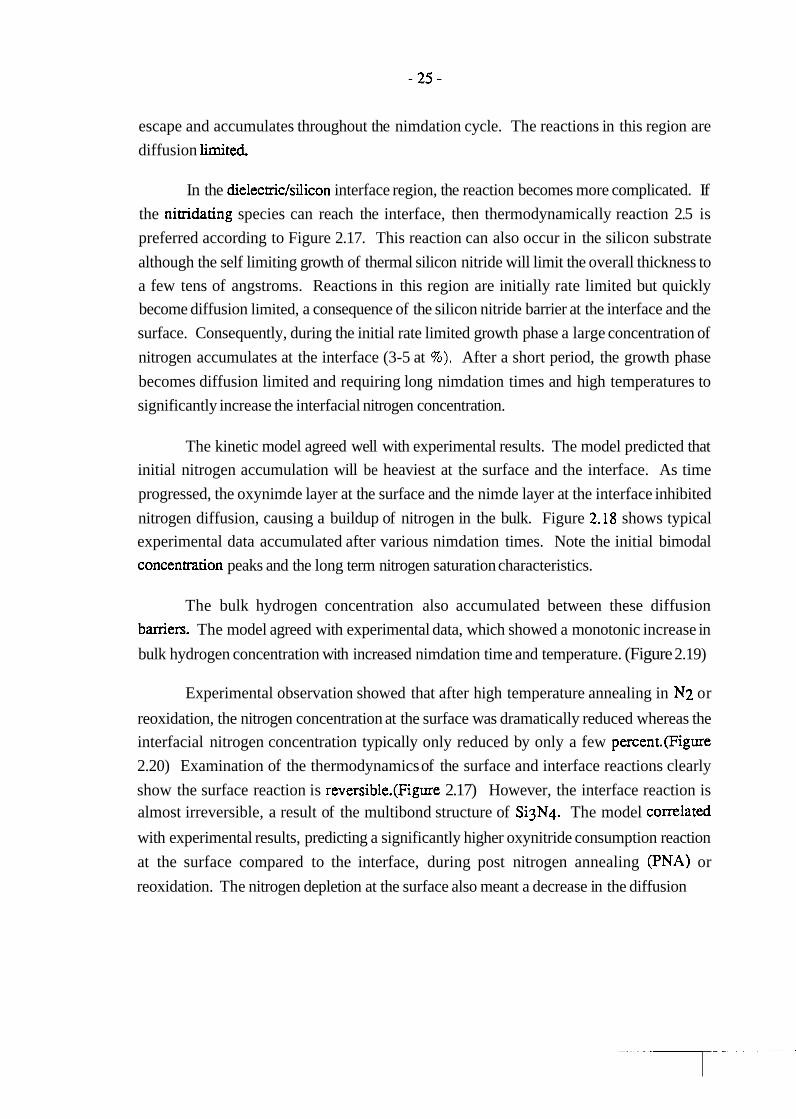
nitrogen diffusion, causing a buildup of nitrogen in the bulk. Figure 2..18 shows typical
experimental data accumulated after various nimdation times. Note the initial bimodal
concentration peaks and the long term nitrogen saturation characteristics.
The bulk hydrogen concentration also accumulated between these diffusion
baniers. The model agreed with experimental data, which showed a monotonic increase in
bulk hydrogen concentration with increased nimdation time and temperature. (Figure 2.19)
Experimental observation showed that after high temperature annealing in N2 or
reoxidation, the nitrogen concentration at the surface was dramatically reduced whereas the
interfacial nitrogen concentration typically only reduced by only a few percent.(Figure
2.20) Examination of the thermodynamics of the surface and interface reactions clearly
show the surface reaction is reversible.(Figure 2.17) However, the interface reaction is almost irreversible, a result of the multibond structure of Si3Nq. The model conelated
with experimental results, predicting a significantly higher oxynitride consumption reaction
at the surface compared to the interface, during post nitrogen annealing (PNA) or
reoxidation. The nitrogen depletion at the surface also meant a decrease in the diffusion
roo l I
I I I 1000 1500
Temperature I 'C I
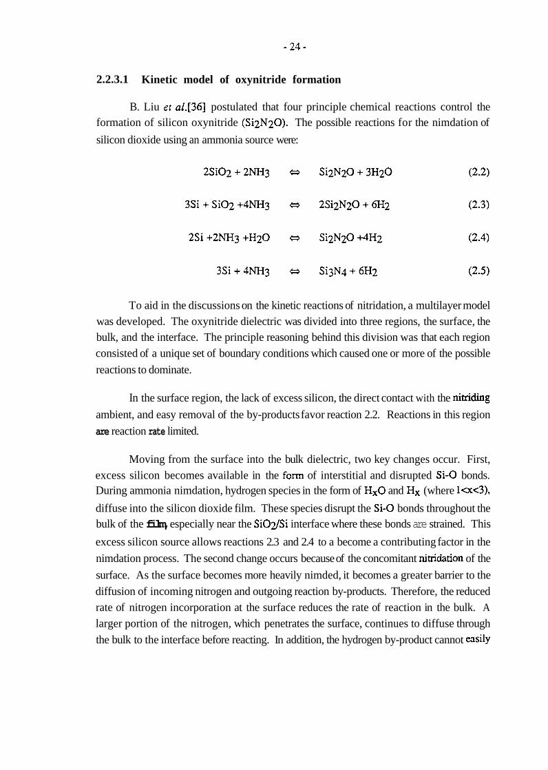
Fig. 2.17 Change in free energy for several nitridation reactions. [36]
Nitridation Temp. 11SO'C dox = 8nm
'O 20 Y
Sputtering Time ( min. )
Fig. 2.18 Typical nitrogen accumulation profile vs. nitridation time. [42]
Oepth (nm)
Fig. 2.19 Typical hydrogen accumulation profile vs. nimdation time. [42]
Depth (nm)
Fig. 2.20 Typical nitrogen accumulation profile vs. reoxidation time. [41]
barrier to the bulk hydrogen. The model agreed with experimental data, which showed that
the PNA or reoxidation was an effective process for significantly reducing the bulk
hydrogen concentration.
The model also adumbrates the consequences of varying the initial thickness of the
silicon dioxide layer. For layers less than 100 A these three regions are not segregated and
therefore the oxynitride elecmcal characteristics should be uniform. As the initial layer
becomes thicker the regions become more segregated, resulting in elecmcal characteristics
of a nitride/oxide/nitride stack typicalIy used in EEPROM applications.
2.2.3.2 Correlation between electrical and physical oxynitride properties
Considerable research has been devoted to the development of an optimal silicon
oxynitride process which exhibits elecmcal and material characteristics superior to silicon
dioxide. These characteristics consist of increased resistance to doparit penetration[37],
improved dielectric reliability[38], higher resistance to hot-carrier induced
degradation[38,39,40], reduced electron trapping[34,37], and improved resistance to
radiation damage [39].
Considerable confusion exists when initially attempting to compare the research
data. In most cases a silicon oxynimde process was optimized for a unique set of
parameters. C. Sodini er al. [13,37] developed a low pressure, low temperature oxynitride
process, T. Hori et al. [41,42] developed a rapid thermal nimdation process, and D.
Kwong et al. [43,44] developed an oxynimde process utilizing nitrous oxide as the
nimdation source. In each case the initial oxide thickness were different, the nitridation and
reoxidation times and temperatures were differ en^ and along with several other key process
parameters. T. Hori et al. [45] developed two very important empirical models relating the
hydrogen and nitrogen concentration of the silicon oxynitride to key eIectrical properties of
the dielecmc, allowing meaningful comparison between silicon oxynitride processes
regardless of the process parameters.
The first model related the hydrogen concentration to the change in flatband voltage
where K was an empirically derive constant and m:] was the hydrogen concentration. The
change in flatband voltage after a fixed dielectric suess is a typical monitor for the level of
electron trapping in the bulk dielectric. The higher the level of electron tapping the greater
the change in flatband voltage. Lowering the level of trapping is critical in increasing the
breakdown elecmc f i e l d ( E ~ ~ ) , decreasing the level of dielectric leakage, and increasing the
overall level of dielecmc reliability.
The second model related both the hydrogen and nitrogen concentrations to the
change in midgap interface state generation
D i t m = (Fox [H:ln)/(l + KN Windm) (2.7)
where KN was an empirical constant, Fox was the Dim at [Nint] = 0 for silicon dioxide
at a given m.], [NintJ was the nitrogen concentration at the oxyniaide/silicon interface, [HI was the hydrogen concentration in the bulk dielectric, and m and n were scaling factors
typically ranging from 2 to 2.5. This model demonstrated that increasing the interfacial nitrogen concentration can result in mirm levels below that of silicon dioxide. In addition,
both models gave a great deal of insight into the effects of the nimdation time and
temperature, the nimdation source, and the reoxidation or PNA.
Using an ammonia nitridation source, the longer the nimdation time and/or the
higher the nimdation temperature, the greater the incorporation of interfacial nitride (Figure
2.21) and bulk hydrogen-(Figure 2.22) The model predicts an initial increase in stress
induced interface state generation due to the early incorporation of hydrogen. However, as
the interfacial nitrogen concentration increases the interface state generation would peak and
then parabolically decrease with time and temperam.(Figure 2.23)
The model also predicts the dramatic reduction in interface state generation
experimentally observed by reoxidation or PNA. Experimental results demonstrated that
the post anneal operations significantly reduced the bulk hydrogen concentration (Figure
2.24) while having relatively little effect on the interfacial nitrogen concentration.(Figure 2.25) With n=2 the model predicts the parabolic reduction observed in ADitm with
increased annealing times.(Figure 2.26)
Nitridation Time ($1
Fig. 2.21 Nitrogen concentration near the Si-Si02 interface vs. nitridation time and temperature. [45]
f 1 1 1 100 200 300 Nitridation Time (d
Fig. 2.22 Hydrogen concentration versus nitridation time and temperature. (451
I f f I 100 100 300 Nitridation Time (I)
(a)
~ I ~ S O X Nitridation Temp.
Nitridation Time (r)
(b)
Fig. 2-23 (a) AVFB and (b) mirm induced by 0.1 C/cm2 electron injection versus nitridadon time and temperature. [45]
The model also predicted a decrease in m i t m with the use of a hydrogen free
nitridation source such as nitrous oxide (N20). In several studies by 2. Liu er al. [46,47]
and D. Kwong er al. [43,44], each showed that thermal nimdation of thermal Si02 in an
N20 ambient resulted in a monotonic decrease in m i t m and AVFB with increased
nimdation time and temperature without requiring reoxidation or PNA.
2.2.3.3 Optimal oxynitride characteristics
After the development of a model correlating process parameters to oxynitride
material characteristics and a model correlating material characteristics to electrical
properties, the fundamental tools have been developed to compare the myriad of oxynimde
processes.
The oxynitride research can be divided into two main groups, those processes which used an ammonia (NH3) nimdation source and those which utilized nitrous oxide
(N20). Within these groups the bulk of the research was divided between conventional
furnace and rapid thermal processing techniques. Rapid thermal processing was developed
to reduce the total thermal budget of conventional furnace processes to fit within the bounds
of modem ULSI processing. Therefore, no significant difference in the final oxynimde
dielectric was anticipated, between the two process techniques.
Examination of the research performed by 2. Liu et al. [48,49] using conventional
furnace techniques and T. Hori er al. [41,42,45,50,51,52] using rapid thermal processing,
highlighted many similarities in the material composition of the final silicon oxynitride
dielectric. In each study, optimal electrical properties were achieved when the interfacial
nitrogen concentration was between 5-15 at % and high temperature reoxidation or nitrogen
annealing was performed. The typical prestressed fixed charge densities and interface state
densities were comparable to silicon dioxide (< 5 1010). In addition, the high-field
endurance was greatly enhanced compared to silicon dioxide. The charge to breakdown (QW) was at least three times larger, high field breakdown voltages were almost double,
and stress induced electron trapping and interface state generation were reduce by 2 orders
of magnitude compared to those of the silicon dioxide control samples.
10SO'C . am
Reoxidation Time (s)
Fig. 2.24 Hydrogen concennation versus reoxidation time and temperature. [41]
1 Nitrogen - NO d m Re-oxidation Temp.
6 - 950'C
Sputtering Time (min.)
Fig. 2.25 Nitrogen Auger depth profiles for the initial oxynimde and the resulting effects of reoxidation temperature. [52]
Resxidation Time (s)
-0.2 I T f SO 100 150 200 Resxidation Time (s)
Fig. 2.26 (a) Dim and (b) AVFB induced by 0.1 ~ c m 2 electron injection vs. reoxidation time and temperature. [52]
-4 I50.C Nitridatloo -050.C NItridatloa
0 .2 .4 .6 -8 1 1.2
Fig. 2.27 Electron and hole mobility as a function of the effective electric field [54]
Earlier studies had reported up to 50% degradation in the electron and hole
mobilities due to coulombic scattering from the high fixed charge densities and electron
trapping.[53] However, closer examination of the oxynitride process showed that no
reoxidation or PNA had been performed to reduce this degradation. In later studies by A.
Wu et d.[54] and S. Lee et a1.[55] the effects of carrier mobility degradation in reoxidized
oxynitride dielecmcs were examined. It was reported that the hole mobility was degraded
13-16% for low electric fields and as much as 24-48% at high fields, compared to silicon
dioxide. Electron mobility exhibited 14-22% degradation at low electric fields but a 17-
24% improvement at high fields.(Figure 2.27) Under normal 5 volts operation, both
mobilities are operating in the low field region, resulting in an overall performance
degradation in MOS applications.
No universally accepted model exists which correlates fixed charge densities to
process parameters. Contrary to the existing theory that fixed charge accumulation in the
oxynitride was the dominant factor in mobility degradation, A. Wu et al., proposed that
mobility degradation was due to nitrogen accumulation in the bulk silicon creating donor-
like traps. This theory gives some insight into why shorter nimdation times, particularly
for rapid thermal processing, typically produce lower fixed charge densities and improved
mobilities.
Research utilizing N20 nimded oxynitrides have reported improved mobility and
device performance compared to ammonia nimded oxynitrides.[46,47,56,57] The
improved PMOS performance has been atmbuted to reduced hole trapping. Reduced hole
trapping effectively increases the hole mobility and reduces the stress induced surface state
generation for PMOS devices. The improved electron mobility is not as well understood. However, N20 nimded oxynimdes typically have low interfacial nitrogen concentrations.
Therefore the nitrogen incorporation into the silicon bulk must also be low, resulting in Si-
N trap formation. Nitrous oxide, however, has several drawbacks. It has been reported
that nitridation of thick silicon dioxide layers is difficult. Interface nitrogen concentrations
for 100 A dielecmcs are typically .l-1 at %. This level was an order of magnitude lower
than that reported as optimal for superior dielectric performance. However, recent experiments using NH3 nimdation of N20 nimded oxynimdes demonstrated that nitrogen
concentration of 10 at % were attainable, while maintaining the advantage of minimal
hydrogen incorporation.[58] However, the impact on the electrical performance of the
dielectric is still pending.
In addition to the total nitrogen concentration, the nitrogen profile within the
oxynitride dielecmc has been shown to be critical in dielecmc performance. An inherent characteristic of nitride incorporation using N20 is a lack of nitrogen accumulation at the
surface. For NH3, similar surface depletion occurred after reoxidation and to some degree
after PNA. A. Wu er a1.[59] showed that low surface nitrogen concentrations increased
charge trapping at the polysilicon gate/oxynimde interface. The end result was a decrease
in the dielectric reliability. For epitaxial lateral overgrowth structures, this surface depletion
presents additional problems. The oxynitride surface eventually becomes the
dielectric/substrate interface after EL0 growth. Therefore, surface depletion would not
only decrease the electrical performance of the interface, but could also reduce the
dielectrics resistance to EL0 ambient degradation.
After review of the plethora of the various oxyniuide processes, several key
processing objectives became apparent:
1. The bu Winterfacial nitrogen concentration should be targeted for 10 at %.
2. Process timehemp should be adjusted to minimize the concentration of hydrogen
in the silicon bulk.
3. With an ammonia nimdation source, a high temperature reoxidation or PNA
process may be required. Care should be taken not to deplete the buW111terfacial
nitrogen concentration below 8 at %.
4. High quality silicon dioxide is a basis for high quality oxynitride
Regardless of the processing technique used, fulfilling these objectives produced a
high quality dielectric.
2.3 References
[I] R.P Zingg, I.A. Friedrich, G.W. Neudeck, and B. Hoeffiger, "Three dimensional stacked CMOS transistors by localized silicon epitaxial overgrowth," IEEE Trans. Elecrron Devices, vol. 37, no. 6, pp. 1452- 1461, June 1990.
[2] J.A. Friedrich and G. W. Neudeck, "Oxide degradation during selective epitaxial growth of silicon," J. Appl. Phys., 64, (7). pp. 3538-3541, 1 October 1988.
[3] K. Hofmann, G.W. Ruboff, and R.A. McCorkle, "Defect formation in thermal Si02 by high-temperature annealing," Appl. Phys. Lett., 49, (22). pp. 1525-1527, 1 December 1986.
[4] K. Hofmann, G.W. Ruboff, and D.R. Young, "Role of oxygen in defect-related breakdown in thin Si02 films on Si (loo)," J. Appl. Phys., 61, (9), pp. 4584-4588, 1 May 1987.
[5] T. Shimono and M. Tsuji, "A New Cleaning Solution for Metallic Impurities on the Silicon Wafer Surface," IEICE Trans. Electron., vol. E75-C, no. 7, pp. 812-815, July 1992.
[6] VLSI Technology, second ed., edited by S.M. Sze, McGraw-Hill Book Co., 1988.
[7] T. Ohmi, M. Miyashita, M. Itano, T. Imaoka, and I. Kawanabe, "Dependence of thin- oxide fdms quality on surface microroughness," IEEE Trans. Elecrron Devices, vol. 39, no. 3, pp. 537-545, March 1992.
[8] I.M. Gibson and D.W. Dong, "Direct evidence for 1 nm pores in 'dry' thermal SiO2 from high resolution transmission electron microscopy," J. Elecnochem. Soc.: Solid-State Science and Technology, vol. 127, no. 12, pp. 2722-2728, December 1980.
[9] M.M. Moslehi and K.C. Saraswat, "Thermal nitridation of Si and Si@ for VLSI," IEEE Trans. Electron Devices,, vol. ED-32, no. 2, pp. 106-123, February 1985.
[lo] T. Kaga and T. Hagiwara, "Short- and long-term reliability of nitrided oxide MISFETs," IEEE Trans. Electron Devices,, vol. 35, no. 7, pp. 929-934, July 1988.
[ l l ] R. Bashir, PhD Thesis, School of Electrical Engineering, Purdue University, December 1992
1121 S. Mori, E. Sakagarni, Y. Kaneko, Y. Ohshima, N. Arai and K. Yoshikawa, "Bottom-oxide scaling for thin nimde/oxide interpoly dielectric in stacked-gate nonvolatile memory cells," IEEE Trans. Electron Devices,, vol. 39, no. 2, pp. 283-291, February 1992.
[13] W. Yang, R. Hayaraman and C.G. Sodini, "Optimization of low-pressure nitridation/reoxidation of Si@ for scaled MOS devices," IEEE Trans. Elecnon Devices,, vol. 35, no. 7, pp. 935-944, July 1988.
[14] E. Suzdci and Y. Hayashi, "On oxide-nitride interface traps by thermal oxidation of thin nitride in metal-oxide-nitride-oxide-semiconductor memory structures," IEEE Tram. Electron Devices,, vol. ED-33, no. 2, pp. 214-217, February 1986.
[15] K.L. Chen, S.A. Saller, I.A. Groves and D.B.Scott, "Reliability effects on MOS transistors due to hot-carrier injection," IEEE J. Solid-state Circuits, vol. SC-20, no. 1, pp. 306-3 13, February 1985.
[16] P.J. Wright and K.C. Saraswat, "The effect of fluorine in silicon dioxide gate dielectrics," IEEE Trans. Electron Devices,, vol. 36, no. 5, pp. 879-889, May 1989.
[17] N. Kasai, P.J. Wright adn K.C. Saraswat, "Hotcanier-degradation characteristics fro fluorine incorporated nMOSFETs," IEEE Trans. Elecrron Devices,, vol. 37, no. 6, pp. 1426-1431, June 1990.
[ 181 P.K. Roy and A.K. Sinha, "Synthesis of high-quality ultra-thin gate oxides for ULSI applications," AT&T Tech. J., pp. 155-174, November/December 1988.
[19] H.H. Tseng and P.J. Tobin, "A robust gate dielecmc for submicron technology," Semiconducror Inrernarional, pp. 68-74, July 1992.
[20] S.L. Wu, C.L. Lee and T.F. Lei, "Characterization of ultrathin oxide prepared by low-temperature wafer loading and nitrogen preannealing before oxidation," J . Appl. Phys., 72, (4), pp. 1378-1385, 15 August 1992.
[21] P. H. Singer, "Trends in wafer cleaning," Semiconductor International, pp. 36-39, December 1992.
[22] L.N. Lie, R.R. Razouk and B.E. Deal, "High pressure oxidation of silicon in dry oxygen," J. Electrochem. Soc., vol. 129, no. 12, pp. 2828-2834, December 1982.
[23] R.F. Pierret, Field Eflect Devices, 2nd ed., Modular Series on Solid State Devices: Volume IV, Addison-Wesley Publishing Co., 1990.
[24] D.K. Schroder, Advanced MOS Devices, Modular Series on Solid State Devices: Volume VII, Addison-Wesley Publishing Co., 1987.
[25] T. Ohmi, M. Morita, A. Teramoto, K. Makihara and K.S. Tseng, "Very thin oxide film on a silicon surface by ultraclean oxidation," Appl. Phys. LRtt., 60, (17), pp. 2126- 2128,27 April 1992.
[26] M. Hirose, T. Yasaka, M. Takakura and S. Miyazaki, "Initial oxidation of chemically cleaned silicon surfaces," Solid Stare Techn., pp. 43-48, December 199 1.
[27] M. Wong, D.K.Y. Liu, M.M. Moslehi and D.W. Reed, "Preoxidation treatment using HCL,/HF vapor," IEEE Electron Device Lett., vol. 12, no. 8, pp. 425-426, August 199 1.
[28] E.T.P. Benny and J. Majhi, "Effect of pre-oxidation HF treatment on the tunnel oxide (SOx) grown at high pressure," Thin Solid Film, 205, pp. 227-232, 1991.
[29] S.S Cohen, "Elecbical propemes of post-annealed thin Si02 films," J . Electrochem Soc., vol. 130, no. 4, pp. 929-932, April 1983.
[30] R. Singh, "Growth of thin thermal silicon dioxide films with low defect density," Microelectronics J., 23, pp. 273-28 1, 1992.
[31] P. Fahey, R.W. Dutton and M.M. Moslehi, "Effect of thermal nitridation processes on boron and phosphorus diffusion in (100) silicon," Appl. Phys. Lett., 43, (7). p.683- , 1983.
[32] Y. Hayafuji, K. Kajiwara and S. Usui, "Shrinkage and growth of oxidation stacking faults during thermal nitridation of silicon and oxidized silicon," J. Appl. Phys., 53, (12), pp. 8639-8646, December 1982.
[33] S. Mizuo, T. Kusaka, A. Shintani, M. Nanba and H. Higuchi, "Effect of Si and SiO;! thennal nitridation on impurity and oxidation induced stacking fault size in Si," J. Appl. Phys., 54, (7) pp. 3860-3866, July 1983.
[34] T. Ito, H. Arakawa, T. Nozaki and H. Ishikawa, "Retardation of destructive breakdown of Si02 films annealed in ammonia gas," J. Electrochem. Soc., vol. 127, no. 10 pp. 2248-2251, October 1980.
[35] M.L. Naiman, F.L. Terry, J.A. Burns, J.I. Raffel and R. Auxoin, "Propemes of thin oxynimde gate dielecmcs produced by thermal nitridation of silicon dioxide," IEDM Tech. Dig., pp. 562-564, 1980.
[36] B.Y. Liu, Y.C. Cheng and Z.H. Liu, "The influence of processes on composition of thermally nimded SiO2 film," J. Electrochem. Soc.: Solid-State Science and Techn., vol. 135, no. 12, pp. 3081-3086, December 1988.
[37] S.S. Wong, C.G. Sodini, T.W. Ekstedt, H.R. Grinolds, K.H. Jackson and S.H. Kwan, "Low pressure nimded-oxide as a thin gate dielecmc fro MOSFETs," J. Elecrrochem. Soc., vol. 130, no. 5, pp. 1139-1 143, May 1983.
[381 T. Ito, T. No& and H. Ishikawa, "Direct thermal nitridation of silicon dioxide films in anhydrous ammonia gas," J. Electrochem. Soc., vol. 127, no. 9, pp. 2053-2057 , September 1980.
[39] F.L. Terry, Jr., R.J. Aucoin, M.L. Naiman and S.D. Senturia, "Radiation effects in nitrided oxides," IEEE Electron Device Lett., vol. EDL-4, no. 6, pp. 191-193, June 1983.
[40] D.J. DiMaria, "The properties of elecmn and hole traps in t h d silicon dioxide layers grown on silicon," The Physics of Si02 and Its Interface, Proceedings of the International Topical Conference, Pergarnon Press, pp. 160- 178, New York 1978.
[41] T. Hori, H. Iwasaki and K. Tsuji, "Electrical and physical properties of ultrathin reoxidized nitrided oxides prepared by rapid thermal processing," IEEE Tram. Elecrron Devices, vol. 36, no. 2, pp. 340-349, February 1989.
[42] T. Hori, H. Iwasaki, Y. Naito and H. Esaki, "Elecmcal and physical characteristics of thin nimded oxides prepared by rapid thermal nitridation," IEEE Tram. Elecrron Devices, vol. ED-34, no. 11, pp. 2238-2245, November 1987.
[43] J. Ahn, W. Ting, T. Chu, S. Lin and D.L. Kwong, "High quality thin gate oxide prepared by annealing low-pressure chemical vapor deposited Si02 in W20," Appl. Phys. Lett., 59, (3), pp. 283-285, 15 July 1991.
[44] J. Ahn, W. Ting, T. and D.L. Kwong, "Furnace nimdation of thermal SiO2 in pure N20 ambient for ULSI MOS applications," IEEE Electron Device Lett., vol. 13, no. 2, pp. 117-1 19, February 1992.
[45] T. Hori, H. Iwasaki and K. Tsuji, "Charge-trapping properties of ultrathin nimded oxides prepared by rapid thermal annealing," IEEE Trans. Electron Devices, vol. 35, no. 7, pp. 904-910, July 1988.
[46] Z. Liu, H.J. Wann, P.K. KO, C. Hu and Y.C. Cheng, "Effects of N20 anneal and reoxidation on thermal oxide characteristics," IEEE Electron Device Lett., vol. 13, no. 8, pp. 402-404, August 1992.
[47] Z. Liu, H.J. Wann, P.K. KO, C. Hu and Y.C. Cheng, "Improvement of charge trapping characteristics of N20-annealed and reoxidized N20-annealed thin oxides," IEEE Electron Device Lett., vol. 13, no. 10, pp. 5 19-521, October 1992.
[48] Z.H. Liu, P.T. Lai and Y.C. Cheng, "Characterization of charge trapping and high- field endurance for 15-nm thermally nimded oxides," IEEE Trans. Electron Devices, vol. 38, no. 2, pp. 344-354, February 1991.
[49] Z.H. Liu and Y.C. Cheng, "Properties of very thin thermally nimded-Si02/Si interface based on conductance and hot-electron injection techniques," IEEE Trans. Electron Devices, vol. 36, no. 9, pp. 1629-1633, September 1989.
[50] T. Hori and H, Iwasaki, "Improved transconductance under high normal field in MOSFETs with ultrathin nitrided oxides," IEEE Electron Device Lett., vol. 10, no. 5, pp. 195-197, May 1989.
[5 11 T. Hori and H. Iwasaki, "The impact of ultrathin nimded oxide gatedielectrics on MOS device performance improve men^" IEDM, pp. 459-462, 1989.
[52] T. Hori and H. Iwasaki, "Ultra-thin re-oxidized nitridedaxides prepared by rapid thermal processing," IEDM, pp. 570-573, 1987.
[53] M.A. Schmidt, F.L. Teny, Jr., B.P. Mathur and S.D. Senturia, "Inversion layer mobility of MOSFETs with nimded oxide gate dielecmcs," IEEE Trans. Electron Devices, vol. 35, no. 10, pp. 1627-1632, October 1988.
[54] A.T. Wu, T.Y. Chan, V. Murali, S.W. Lee, J. Nulman and M. Garner, "Nimdation induced surface donor layer in silicon and it's impact on the characeristics of n- and p- channel MOSFETs," IEDM, pp. 271-274,1989.
[55] S.W. Lee, T.Y. Chan and A.T. Wu, "Circuit performance of CMOS technologies with silicon dioxide and reoxidized nimded oxide gate dielectrics," IEEE Electron Device Lett., vol. 11, no. 7, pp. 294-296, July 1990.
[56] A. Uchiyama, H. Fukuda, T. Hayashi, T. Iwabuchi and S. Ohno, "High performance dual-gate subhalfmicron CMOSFETs with 6 nrn-thick nimded SiO2 films in an N20 ambient," IEDM, pp. 425-428, 1990.
[57] H. Hwang, W. Ting, D.L. Kwong and J. Lee, "High quality ultrathin oxynimded gate dielecmc prepared by rapid thermal processing in N20," Int. Con$ Solid State Devices and Materials, pp. 1155- 1 156, 1990.
[58] G.W. Yoon, A.B. Joshi, J. Kim and D.L. Kwong, "MOS characteristics of NH3- nimded N2O-grown oxides," IEEE Electron Device Lett., vol. 14, no. 4, pp. 179-181, April 1993.
[59] A.T. Wu, V. Murali, J. Nulman, B. Triplett, D.B. Fraser and M. Garner, "Gate bias polarity dependence of charge trapping and time-dependent dielecmc breakdown in nimded and reoxidized nitrided oxides," IEEE Electron Device Lett., vol. 10, no. 10, pp. 443-445, October 1989.
CHAPTER 3: PROCESS DEVELOPMENT
3.1 Device Fabrication
3.1.1 Overview and purpose
Two basic test structures, metal/polyoxide/polysilicon parallel plate capacitors and
conventional PMOS capacitors, were constructed to test the effects of ammonia nimdation
on the EL0 growth ambient durability of the oxide dielectrics. The use of conventional
PMOS capacitor suuctures allowed direct comparison of the nitridation characteristics of
silicon dioxide with published results. However, prior to this study, no material or
electrical properties of nimded polyoxide dielectrics had been reported. In addition, neither
nimded dielectric materials, NOX or NPOX, had been evaluated under EL0 growth
ambient stress conditions.
For both device structures, the fabrication process was optimized to produce the
highest quality control dielectric possible. The computer automation combined with the
Class 100 clean room facilities, resulted in tightly controllable process parameters. The
yields on the control devices were nearly 100% and the process variation was minimized.
As a result, the improvements observed in the EL0 growth ambient stress durability of the
nimded oxide and nimded polyoxide dielectrics were more easily attributable to changes in
the nitridation process.
3.1.2 Metal/polyoxide/polysilicon-silicon test structures
MetaVpolyoxide/N+ polysilicon-silicon parallel plate capacitors (137 137 pm2) were built on .02 f2-cm, As-doped n-type, <loo> oriented silicon wafers. (Figure 3.1) A
highiy doped substrate was chosen to insure a low resistance contact to the bottom plate of
the capacitor structure. In addition, no bottom side diffusion or metal contact was required
to insure good ohmic contact for electrical testing.
Metal
250A Polyoxide
N+ <loo> Sub N+ Polysilicon
Fig. 3.1. Polyoxide test structure
The N+ substrate received an A-clean consisting of a 5 min. heated H2S04:H202
soak, a 5 min. aqueous H a soak, followed by a 10 min. aqueous HCL:H202 soak. To
remove the native oxide formed during the clean operation and insure a good physical
contact between the two layers, the wafers received a 50:l HF dip prior to deposition of
3500 A of amorphous siIicon. Amorphous silicon was chosen over conventional
polysilicon due to the smoother surface topography compared to deposited polysilicon. Surface roughness has been shown to be a key factor in determining the elecmcal
properties of the resulting oxide.[ 1]
To maintain the smooth surface, the wafers wen doped with a 4* 10 ions/cm2, 40 KeV phosphorus implant. Conventional gas phase doping techniques using P O U 3 and
PH3 sources created a phosphorus saturation condition at the surface of the polysilicon.
Removal of this layer prior to oxidation results in increased surface roughness. However,
oxidation through the saturation layer produced a phosphorus saturated polyoxide. Both
conditions resulted in polyoxides with low breakdown fields, high leakage currents and
highly nonuniform polyoxide dielectric thicknesses. Figures 3.2 and 3.3 highlight the
resulting post oxidation differences in surface smoothness produced by the implant and gas
phase doping sources. In both samples the polyoxide was removed prior to FE microscope
examination. The distended grain structures are the result of differences in oxidation rates
due to differences in crystal orientation. Studies have shown that polyoxide uniformity
replicates the surface topology of the polysilicon.[2]
Fig. 3.2 PH3 doped amorphous silicon after 250 A oxidation was removed.
Fig. 3.3 Phosphorus implanted amorphous silicon after 250 A oxidation was removed.
The implanted amorphous silicon was annealed and converted to 30 R/sq
polysilicon during thermal oxidation. Two key process steps were incorporated in the
oxidation process to enhance to the surface smoothness of the resulting polysilicon and the
uniformity in polyoxide thickness. First, a low level oxygen flow was maintained during
thermal rampup, creating a thin oxide layer. Studies have shown that this layer freezes the
silicon atoms at the surface while still in the amorphous state. As a result, the amorphous
surface smoothness was maintained during the polysilicon transition.[3] Secondly, the
oxidation temperature was chosen to be 1000 "C to encourage viscous flow of the
polyoxide dielectric and place the oxidation reaction in the diffusion controlled regime.
Studies have shown that transition from amorphous to polysilicon results in grains
predominantly oriented < 1 1 1 > and < 1 lo>. The difference in oxidation rates between these
crystal orientations can cause surface roughening of the polysilicon. However, maintaining
the oxidation in the diffusion controlled regime, narrows the difference in oxidation rates
between the two crystal orientations and thereby minimizes the surface roughening. Grain
boundary enhanced oxygen diffusion has also shown to cause a 25% reduction in
polyoxide thickness along grain boundaries. Viscous flow of the polyoxide enhances the
uniformity across the grain boundaries. [4]
After oxidation, the polyoxide wafers were divided into four groups. Group IA
wafers were submitted for 1 0 ~ metal deposition, photolithography, and 400 OC metal
anneal. Group I represented the polyoxide control group.
Group IIIA-IVA wafers were nitridated for various times and temperatures in
anhydrous ammonia followed by a post nimdation anneal (PNA) at nimdation temperature.
Following nitridation Group IIIA wafers were metallized, patterned and annealed. Group
IIIA represented the nimded polyoxide (NPOX) control group.
Group IIA and IVA wafers received an EL0 growth cycle conducted both in an inductively heated, pancake-type and lamp heated, barrel-type epitaxial reactors. Although
the growth parameters varied between reactors, similar growth rates were maintained.
Group IIA represented the EL0 stressed polyoxide group, while Group IVA wafers
represented the EL0 stressed NPOX group.
3.1.3 Metal/oxide/silicon test structures
The conventional Metal/Oxide/Semiconductor capacitors ( 137 x 137 pm2) were
The subsuates received an A-clean and a 50: 1 HF dip prior to oxidation. Oxidation
consisted of a low temperature load under nitrogen. During thennal ramp, a low oxygen
flow was present to form a high quality thin oxide layer. This protected the silicon surface from HCL pitting, during the 1000 OC 02/HCL oxidation cycle. Studies have shown that
the addition of HCL during oxidation is a key factor in reducing mobile, fixed and interface
charge densities, in addition to reducing the number of oxide defects.[4,5] The goal was to
optimize the dielectric breakdown strength of the base oxide, making the effects of
nitridation and EL0 stress more discernible.
Prior to metdlization the wafers were again divided into four groups. Group IB wafers were submitted for 10 K%, metal deposition, photolithography, and 400 OC anneal.
Group IB represent the silicon dioxide control group.
Group IIIB-IVB wafers were nitridated for various times and temperatures in
anhydrous ammonia followed by a PN.4 at temperature. Following nitridation Group mB
wafers were metallized, patterned and annealed. Group IIIB represented the nitrided
silicon dioxide (NOX) control group.
Group IIB and IVB wafers received an EL0 growth cycle conducted both in an
inductively heated, pancake-type and barrel-type epitaxial reactors. Although the growth
parameters varied between reactors, similar growth rates were maintained. Group W
represented the EL0 stressed silicon dioxide group, while Group IVB wafers represented
the EL0 stressed NOX group.
P <100> Sub
Metal
250A Silicon dioxide
Fig. 3.4. Silicon dioxide test structure
3.2 Ammonia Nitridation Process
3.2.1 Nitridation process and analysis tools
The effect of nitridation time and temperature on the silicon, nitrogen, and oxygen
profiles throughout the polyoxide and silicon dioxide dielecmcs were evaluated using a
Phi-550 Electron Spectroscopy for Chemical Analysis (ESCA) system. Several samples
were taken h m each wafer to check for nimdation uniformity across the wafer. A 5 pm x
5 p raster area was used to insure a uniform depth profile and the elemental composition
of the sputtered dielecmc was analyzed every 6A providing a very detailed picture of the
NOX and NPOX dielectric composition.
Two primary nimdation techniques were utilized in this study. For short duration
nimdation, 5-120 seconds, a Peak Alp-6000 rapid thermal processor was required.
Several features of this system assisted in minimizing the process uniformity and variability
inherent in single wafer rapid thermal processors. First, the system utilized an an: lamp
heat source with a spectral output located in the band to band absorption spectra for silicon,
as apposed to the inmnsic free canier absorption spectra. The resulting heating
characteristics of the RTP system were less dependent on the level of doping or defects in
the silicon wafers, reducing the wafer to wafer variability. Radiation diffuser were also
incorporated to enhance the uniformity of the heat source.
Superior temperature control was maintained by a three stage closed loop feedback
system. Preload backside reflectance measurements were performed prior to each run, and
the changes in ernissivity for various process conditions were adjusted based on extensive
calibration files. Temperature control during processing was maintained using a
pyrometer. The stainless steel chamber eliminated pyrometer signal contamination
normally produced by conventional quartz walled chambers. The cold-walled chamber
design also prevented coating during processing, thereby reducing the contamination
particles and the chamber "memory" effects from previous runs. ESCA analysis verified
that the rapid thermal nimdation process was very uniform across the wafer and highly
repeatable from run to run.
High thermal ramps cycles on the order of 20 OC/sec were utilized when ammonia
nitridating the thermal silicon dioxide and polyoxide test dielecmcs. The high thermal
stress produced by this process enhance the substitutional nitrogen incorporation in the
oxides causing significant bulk nitrogen accumulation in short periods of' time. In addition,
the thermal stress appeared to densify the nitrided material dramatically increasing the EL0
stress durability of the material at relatively low levels of nitrogen incorporation. However,
the thermal stress was also observed to create slip planes in the silicon substrate along the
edge of the wafer. As a result, there was a tradeoff between the amount of nitrogen
incorporation and the amount of wafer area lost to slip damage.
For longer nimdation times a conventional atmospheric, resistively heated, hot
walled quartz diffusion furnace was used. The maximum thermal ramp rate on the order of
6 "C/min. The decrease in thermal stress enhanced nitrogen incorporation meant that higher
nimdation temperatures and longer process times were required to incorporated the same
level of nitrogen as that observed in seconds on the RTP system. However, nitridation
times in excess of 2 hrs produced no slip damage. In both cases, the nimding source gas
was ammonia (NH3). Several recent nimdation studies have used nitrous oxide (N20) as
the nitridation source gas.[6,7] However, the high oxide dielecmc nitrogen concentrations required for good EL0 stress durability made N 2 0 unfeasible for this study.
3.2.2 Comparison of nitridation characteristics between thermal silicon dioxide and polyoxide dielectrics
The ammonia nimdation characteristics of thermal polyoxide films were very
similar in many respects to those of thennal silicon dioxide. The incorporation of nitrogen
in both dielectrics with respect to time was characterized by three distinct phases.[8]
During Phase I, the initial nitrogen accumulation occurred at the surface and interface with
little accumulation in the bulk. For NOX dielectrics this interfacial nimdation region was
primarily located in the oxide film. This was attributed to the formation of a silicon nimde
barrier which slowed further penetration of the nimdating species into the substrate.
However, NPOX dielecmcs exhibited a broadened interfacial nimdation region with a
significant accumulation forming in the polysilicon region. Studies have demonstrated that
the presence of grain boundaries enhanced the diffusion of oxygen species into the
polysilicon resulting in an increase in the polyoxide/polysilicon interface region.[9] For
phosphorus implanted amorphous silicon, the interface region was shown to be
approximately 60% wider than single crystal oxide interfaces. The broadened interfacial
nimdation region was therefore attributed to a broadened interfacial transition region.
As the nimdation time increased, Phase I1 was characterized by the rapid increase in
the bulk nitrogen concentration while the surface and interface concentration began to
saturate. Finally, Phase III exhibited nitrogen saturation in all three regions. In this phase,
increases in the nimdation time resulted in only small increases in the total nitrogen
Fig. 3.5 Rapid thermal nimdation of thermal silicon dioxide versus thermal polyoxide at 1050 O C for 40 seconds.
As shown in Figure 3.5, the principle difference between the nitridation of
polyoxide versus silicon dioxide was the total level of nitrogen incorporation throughout
the dielectric. For a fixed time and temperature, thermal polyoxide incorporated a higher
atomic percentage of nitrogen at the surface, bulk and interface. However, this difference
became less significant compared to the total nitrogen concentration levels during phase I1
and III. For the shorter RTN process illustrated in figure 3.5, characterized as phase I
accumulation, the bulk nitrogen concentration in the thermal polyoxide represented an
increase of 50% compared to the bulk concentration in thermal silicon dioxide. For longer
furnace nitridation processes, characterized as phase I1 and III, the rapid bulk accumulation
and eventual saturation around 15-20 at% resulted in a differential of less than 10%. It is
important to note that no noticeable improvement in the EL0 stress durability for NPOX dielectrics was attributable to these small changes in nitrogen concentration.
It was observed, however, that the differences in the two nitridation process
techniques produced noticeable differences in the profile and performance of the NPOX
and NOX dielectrics. The rapid thermaI nimdation (RTN) process was found to produced
a nitrogen rich surface layer in both NOX and NPOX dielectric materials almost
immediately. The equivalent of a 20A silicon nimde layer was formed on the surface of the
NOX and NPOX dielectrics, as demonstrate in a similar study by Moslehi, er al., using
comparable RTN process parameters on 100 A thin thermal silicon dioxide.[lO] The rapid
formation of this diffusion barrier effectively slowed that rate of bulk and interfacial
nitrogen accumulation by inhibiting the diffusion of the nitriding species. For nimdation
temperatures ranging from 1000 OC to 1200 "C over periods from 5 sec to 120 sec, the
maximum bulk nitrogen incorporation attainable was 3-3.5 at%.(Figure 3.6) Despite these
low concentrations, rapid thermal nitridation produced dieIectrics with a higher EL0 stress
durability than furnace nimdation, at comparable bulk nitrogen levels.
Fig. 3.6 Rapid thermal nitridation of polyoxide at 1050 "C for 40 seconds.
Although longer RTN nimdation times produced higher nitrogen concentrations
within the dielectric, the added thermal stress began to produce silicon slip planes along the
edges of the wafer. These slip planes were the result of stress relief within the silicon
substrate and caused excessive leakage and/or complete device failure if located near or on a
slip plane.
Furnace nimdation, on the other hand, was characterized by a much lower thermal
stress. As a result, the rapid formation of the surface silicon nimde diffusion barrier was
not present. Figure 3.7 illustrates the typical nitrogen accumulation observed in both NOX
and NPOX dielectrics over time during furnace nimdation at 1100 OC. It is important to
note that furnace nitridation tends to incorporate a uniform nitrogen concentration over time
in both NOX and NPOX dielectrics. As will be demonstrated in the next chapter, the bulk
nitrogen concentration was determined to be the key factor in reducing surface roughening
and pinhole formation during EL0 growth ambient stressing. The high, uniform bulk
nitrogen concentration slowed the rate of pinhole growth and reduced the degree of
measurable surface roughening.
The EL0 stress durability of furnace nimded NOX and NPOX films were also
found to improve with higher nimdation temperatures combined with a high temperature
post nimdation anneal (PNA). Studies have demonstrated that the base silicon dioxide
material could be viewed as a long range amorphous material made up small crystalline regions of interlocking tetrahedron sio44- structures.[5](Figure 3.8) The tetrahedron
consisted of a triangular configuration of oxygen atoms surrounding a silicon atom. This
amorphous state of Si02, also referred to as fused silica, is thermodynamically unstable
below 1710 OC. As a result, there exists a tendency for transformation from the amorphous
state to the denser crystalline state, at temperatures above 1000°C.(Figure 3.9)
The density of amorphous silicon dioxide is determined by the quantity of bridging
oxygen, the closer to 100% the closer to quartz. Since the dominant nitrogen incorporation
mechanism is via substitution with existing oxygen atoms, it would be expected that high
concentrations of nitrogen incorporation would remove a significant quantity of bridging
oxygen sites, thereby lowering the density of the material. The effect of high thermal stress
or elevated nimdation temperature followed by a high temperature nitrogen anneal was
thought to be the densification of the nimded silicon dioxide or poIyoxide film by the
increased formation of bridging oxygen sites and possibly the formation of bridging
networks at the nitrogen sites.[ll]. Initial dielectric studies characterizing the EL0
degradation effects on deposited LTO Si02, SiN202 and SiN3 films showed that a
significant improvement could be achieved by densifying the LTO film with an 1 lW°C, 60 rnin. N2 bake. It was therefore concluded that the higher nitridation temperatures and PNA
Fig. 3.7 1100 OC furnace nimdation of silicon dioxide at 5-10 and 15 rnin. intervals.
Bridging oxygen
Nonbr~dging oxygen
Silicon
Network modifier
Hydroxyl group
Network former
Fig. 3.8 Model depicting the typical amorphous fused silica bonding structure.
Fig. 3.9 Model depicting the typical crystalline quartz bonding structure.
effectively densified the NOX and NPOX dielectrics, thereby improving the EL0 stress
durability. The high thermal stresses inherent the RTN process was thought to have a
similar densifying effect on the dielecmc, eliminating the need for a post nimdation anneal.
3.3 Epitaxial Reactors and Growth Parameters
Two different style epitaxial reactors were utilized in this research, an Applied Materials
AMT-7800RP radiantly heated barrel epitaxial reactor and a Gemini 62 rf heated pancake epitaxial reactor. The AMT system was physically located within the clean room facilities
in which the wafers were fabricated. Prior research had utilized this equipment for
growing EL0 and confmed lateral selective epitaxial growth (CLSEG) material.[l2] These
studies demonstrated that this system was capable of growing good epitaxial material and at
the same time providing a typical EL0 growth ambient stress conditions. The ability to
vary the process parameters and monitor the effect on the NOX and NPOX films provided
a unique opportunity to isolate key process variables which contribute to dielectric
degradation or increase durability.
The principle operaring conditions utilized on the AMT reactor were as follows:
ELO-1: System temperature, pressure: 975 OC, 50 Torr 1. 3.0 min. H2 bake
2. 40180 min. H2, HCL, SiH2C12 (DCS) deposition
The main process variable evaluated was the effect of the HCL to DCS ratio on the
nimded silicon dioxide and polyoxide dielecmcs.
The Gemini system, physically located at Purdue University, was utilized as a
control reactor. Extensive studies had been conducted evaluating the epitaxial material
quality, modeling the process parameters and their effect on the growth conditions, and
modeling the gas flow and thermal distribution within this reactor. The development of the
3-D CMOS structure and the subsequent studies evaluating the EL0 ambient inducted
degradation of oxides, were conducted in this reactor.
The principle operaring conditions utilized on the Gemini reactor were as follows:
ELO-2: System temperature, pressure: 970 OC, 40 Torr 1. 5 min. H2 bake
2. 30 sec HCL etch
3. 40180 min. H2, HCL, SiH2C12 (DCS) deposition
Although the final product was the same, the differences in reactor design, gas flow
dynamics, temperature and operating pressure between the two reactors resulted in
significant differences in the performance and durability of nitrided oxides. ?he AMT
system tended to be more destructive to the dielectrics, possibly due to the higher volume
of reactant gases. However, at 50 Torr, good growth selectivity was maintained down to
an HCL to DCS ratio of 2.0. The Gemini, on the other hand, operating at a lower chamber
pressure, a slightly lower operating temperature, and under dramatically different gas flow
characteristics, experienced extreme growth selectivity problems up to an HCL to DCS
ratio of 3.5-4.0. The loss of growth selectivity resulted in excessive sporadic surface
nucleation on the thin NOX and NPOX dielectric films inhibiting the ability to electrically
test the capacitor structures. However, at the lower operating pressure, small changes in
the HCL to DCS ratio produced major changes in the growth selectivity and the pinhole
formation characteristics of the system.
3.4 Reoxidation Techniques
Based on the literature review conducted in chapter 2, it was concluded that a
reoxidation process would have to be developed to optimize the elecmcal performance of
the NOX and NPOX dielectrics. In addition, a reoxidation process proposed as a possible
solution to the selectivity problem experienced on the Gemini system. It was theorized that
the sporadic surface nucleation would be eliminated if the surface layer were convened
back to silicon dioxide. Experiments with varying surface nitrogen concentrations
concluded that a final surface nitrogen concentration at or below 0.5 at% was required to
eliminated the selectivity problem for both the NOX and NPOX dielectrics. In the process
of developing a reoxidation process, the following techniques were evaluated.
3.4.1 Conventional furnace reoxidation
Conventional furnace reoxidation techniques, documented in various studies, were
examined fmt.[13,14] The nitridation process was modified to include a post nitridation
reoxidation step at the nitridation temperature. During the reoxidation step, oxygen
diffused through the nitrided oxide replacing existing nitrogen atoms, gradually converting
the material back to an oxide. Figure 3.10 shows the effects of the furnace reoxidation
process on the bulk nitrogen concentration. It is important to note that a significant
concentration of bulk nitrogen was lost during the process. It was observed in this study
that a key parameter in improving EL0 stress durability of both NOX and NPOX
dielectrics was maintaining a bulk nitrogen concentration of 8 at% or greater. Utilization of
conventional reoxidation techniques therefore required that the initial nitridation time had be
dramatically increased to compensate for the decrease in bulk nitrogen.
3.4.2 0 2 plasma reoxidation
In an attempt to reduce the loss of bulk nitrogen concentration, a novel plasma
reoxidation technique was evaluated. Due to the radiation hardening inherent in nitrided
oxide dielectrics, it was concluded that the NOX and NPOX dielectrics could be subjected to moderate levels of rf activated 0 2 plasma without degrading the elecmcal properties of
the film.[l5] Utilizing a conventional rf barrel plasma etch system, the nimded oxides were subjected to 300-1000 watts of 0 2 plasma for 30 minutes. Figure 3.1 1 shows the
typical results achieved using the technique on low level nimded dielectrics, primarily the
RTN wafers.
NOX Dielectric ++ Silicon .,
... \. '-. H1 ...........
. .W l -.. -/..-- ...., .- ........ .-A
Reox NOX
.... - w / - -
i.. . . r
Fig. 3.10 The effect of reoxidation on the nitrogen concentration in a 250 A NOX dielecmc
1
Dielectric + I-+ Silicon ::
Fig. 3.1 1 The effect of 0 2 plasma reoxidation on the nitrogen concentration in a 250 A NPOX dielecmc
As can be seen, the oxygen plasma only effected approximately the first 25 A of the
dielecmc surface. The resulting reduction in sporadic surface nucleation can be seen in
Figures 3.12 and 3.13. ESCA results showed that in addition to desired oxygen for
nitrogen replacement, plasma reoxidation also resulted in the formation of nitrogen-oxygen
bonds. These bonds resulted in an increased resistance to nitrogen depletion with increased
reoxidation time. A process limit on the amount of nitrogen reduction possible with this
technique was soon established. In general, the surface nitrogen concentration could not be
reduced below 50% of the bulk concentration. However, even at these levels, the amount
of sporadic surface nucleation generated on the NOX and NPOX dielecmcs in the Gemini
epitaxial reactor was significantly reduced.
3.4.3 Discussion and future reoxidation considerations
A reoxidation technique for future reoxidation studies of NOX and NPOX
dielectrics is proposed. Observations made during the characterization of the rapid thermal
nitridation revealed that 1200 OC ammonia nimdation for 5 seconds results in primarily a
surface limited reaction. The nitrogen incorporation in the bulk and interface was found to
be minimal. It was concluded that the high temperature ambient produced nitrided the
surface so fast and thorough that it produced a surface diffusion barrier which could not be
penetrated in the short processing time. It is theorized that a similar reaction will occur in a
high temperature oxidizing ambient. A 1200 OC, 5 sec. rapid thermal oxidation cycle
should create an oxidizing species so reactive as to deplete itself within the first 25 A from
the surface. This should greatly minimize the loss of bulk nitrogen. In addition, the high
temperature process combined with the minimal oxygen that will inevitably diffuse into
bulk should be beneficial in reducing the demmental bulk hydrogen concer.rratian.[16,171
Fig. 3.12 Example of sporadic surface nucleation on a 250 A NPOX dielecmc.
Fig. 3.13 250 A NPOX dielecmc after 0 2 plasma reoxidation.
3.5 References
[I] T. Ohmi, M. Miyashita, M. Itano, T. Imaoka, and I. Kawanabe, "Dependence of thin- oxide fdms quality on surface rnicroroughness," IEEE Trans. Electron Devices, vol. 39, no. 3, pp. 537-545, March 1992.
[2] E.A. Irene, E. Tierney, and D.W. Dong, "Silicon oxidation studies: morphological aspects of the oxidation of polycrystalline silicon," J. Electrochem. Soc., vol. 127, no. 3, pp. 705-713, March 1980.
[3] Effiong Ibok, Shyam Garg, "A characterization of the effect of deposition temperature on polysilicon properties," J. Electrochem. Soc., vol. 140, no. 10, pp. 2927-2937, October 1993.
[41 VLSI Technology, second ed., edited by S.M. Sze, McGraw-Hill Book Co., 1988.
[5] Silicon Processing for the VLSI Era Volume I : Process Technology, edited by S. Wolf and R.N. Tauber, Lattice Press, 1986.
[6] H.G. Pomp, A.E.T. Kuiper, H. Lifka, A.H. Monuee, P.H. Woerlee, "Lightly nimded gate oxides for 0.25 pm CMOS," Microelectronic Engineering, vol. 22, pp. 85- 88, 1993.
[7] J. Ahn, W. Ting, D. L. Kwong, "Furnace nimdation of thermal Si02 in pure N20 ambient for ULSI MOS applications," IEEE Electron Device Leners, vol. 13, no. 2, pp. 117-1 19, February 1992.
[8] B.Y. Liu, Y.C. Cheng and Z.H. Liu, "The influence of processes on composition of thermally nimded Si02 film," J. Electrochem. Soc.: Solid-State Science and Techn., vol. 135, no. 12, pp. 3081-3086, December 1988.
[9] G. Queirolo, G. Ghidini, L. Meda, and C. Signorini, "Polycrystalline silicon oxidation kinetics and Si/SiO2 interface width," J. Electrochem. Soc.: Solid-State Science and Techn., vol. 133, no. 11, pp. 2381-2385, November 1986.
[lo] M.M. Moslehi, K.C. Saraswat and S.C. Shatas, "Rapid thermal nimdation of SiO2 for nitroxide thin dielectrics," Appl. Phys. Lett., 47, 10, p.1113-1115, 15 November 1985.
[ l 11 I.A. Chaiyasena, P.M. Lenahan, and G.J. Dunn, "Identification of a paramagnetic nitrogen dangling bond defect in nimded silicon dioxide films on silicon," Appl. Phys. Lett., 58, 19, p. 2141, 1991.
[12] P.J. Schubert, PhD Thesis, School of Elecmcal Engineering, Purdue University, May 1990
[13] W. Yang, R. Hayaraman and C.G. Sodini, "Optimization of low-pressure nimdationheoxidation of Si@ for scaled MOS devices," IEEE Trans. Electron Devices,, vol. 35, no. 7, pp. 935-944, July 1988.
[14] A.T. Wu, V. Murali, J. Nuiman, B. Tripiett, D.B. Fraser and M. Garner, "Gate bias polarity dependence of charge trapping and time-dependent dielectric breakdown in nimded and reoxidized nimded oxides," IEEE Elecrron Device Lert., vol. 10, no. 10, pp. 443-445, October 1989.
[15] F.L. Terry, Jr., R.J. Aucoin, M.L. Naiman and S.D. Senturia, "Radiation effects in nimded oxides," IEEE Elecaon Device Lert., voi. EDL-4, no. 6 , pp. 191-193, June 1983.
[16] A. Kuiper, et al., "Hydrogenation during thermal nitridation of silicon dioxide," J. Appl. Phys., 59 (8), pp. 2765-2772, 15 April 1986.
[17] E. Cartier, D. Buchanan, G. Dunn, "Atomic h ydrogen-induced interface degradation of reoxidized-nimded silicon dioxide on silicon," J. Appl. Phys. Lett., 64 (7), pp. 901- 903, 14 February 1994.
CHAPTER 4: E L 0 GROWTH AMBIENT STRESS RESULTS
4.1 Overview and Purpose
The primary goal of this research was to evaluate the effects of ammonia nimdation
of on the EL0 ambient durability of thin thermal silicon dioxide and polyoxide dielectrics.
Prior EL0 stress studies have demonstrated that the dielectric thickmess significantly
im.pacted the durability of these films.[l] It was observed that the thi.cker the dielectric
material, the higher the electrical yield for a given stress duration. IVitridation studies
involving thermal silicon dioxide films have also shown that dielectric tlhickness was a key
prcxess parameter in establishing the nimdation characteristics of the dielectric.[2,3]
Figure 4.1 illustrates that at 1 150°C, the thicker the silicon dioxide die1e:cmc the lower the
average nitrogen concentration in the silicon dioxide film In an attempt ito limit the number
of process variables allowing for better correlation between nitrogen incorporation and EL0 smss durability, the dielectric thickness was fixed at 250A.
The first half of this chapter is devoted to the material evaluation and electrical
chiuacterization of NOX dielectrics in full awareness of the quantity of existing published
research on this subject. The reasoning was two fold. First, since the dielectric thickness
is ii critical component in the nitridation process and therefore significantly impacts the
resulting electrical characteristics of the film, a detailed material and eIecmcal
characterization of a 250A NOX dielectric adds to the general body of knowledge. In
addition, since the early 1980's very little nimdation research has been conducted using
corlventional quartz diffusion furnaces.
Secondly, several studies conducted at Purdue University have demonstrated that
the electrical characteristics of polysilicon/polyoxide/ELO MOS smctures are comparable
to ]:hose of conventional substrate MOS structures.[4,5] In particular, the fixed oxide
charge and interface state densities were comparable to those of thermal silicon dioxide. It
was therefore concluded that the detailed electrical characteristics of 25081 ~ t r ided thermal
silicon dioxide dielectrics would provide considerable insight into the expected electrical
chi~terist ics of nitrided polyoxide in a similar application.
0 0 S 0 100 150 200 250
Nitridation Time (mn)
0 22 nrn a40 nm 0 7 8 nm A131 nm
Fig. 4.1 Average nitrogen content as a function of nimdation time for various thicknesses of thermal silicon dioxide. Ammonia nimdation conducted at 1 150°C.
4.2 Initial Material and Electrical Characterization
4.2.1 Nitridation characterization
It is important before preceding to emphasize some key observations made during
the material and EL0 stress durability evaluation of nimded thermal silicon dioxide and
polysilicon dioxide dielectrics. First, the key parameters determining the durability of the
NClX and NPOX dielectrics were the bulk nitrogen concentration and its uniformity.
Secondly, comparisons of bulk nitrogen concentrations in NOX and NIWX films over a
wide range of process times and temperatures, showed that the bulk concentration in
NP3X was always higher than that of NOX. However, the measured difference between
the bulk nitrogen concentrations of the two dielectric materials never exceeded a range of
1.0-1.5 at% These profiles, although different in absolute concentration, exhibited
idelltical profiles throughout the both dielectrics. Finally, no measurable improvement in
the EL0 stress durability could be attributed to this difference in nitrogen concentration.
As a result of these observations, i t was decided that detailed ESCA analysis would
b: primarily conducted on the NOX dielecmcs, with only periodic che:cks being made on
NPOX frlms. This would allow direct comparison of the ESCA res~llts with published
results while still maintaining an accurate indicator of the nitridation characteristics of
NPOX.
Table 4.1 highlights the effect of rapid thermal nimdation time .and temperature on
the nitrogen dismbution of 25081 NOX dielectrics. The trend in concentration from surface
to interface assumes the "U" shape characteristic of rapid thermal nitridation. The 6-10
tirnes increase in surface nitrogen concentration versus the bulk concentration has been
attributed to the formadon of a thin silicon nimde layer approximately :ZOA thick.[6] This
layer acts a diffusion barrier inhibiting the diffusion of the nimdating species into the bulk
of the dielectric. The formation of this nimde banier at the surface is believed to be the key
reason rapid thermal nitrided NOX and NPOX dielectrics exhibit such, high resistance to
According to the kinetic model for the nitridation of silicon dioxide, discussed in
chapter 2, the most favorable reaction involves silicon nimde formation at the silicon
dioxide/ silicon interface, compared to the bulk.[7] Therefore, of the nimdation species
which eventually diffuse past the surface nitride layer, a significant portion is expected to
cointinue diffusing through the bulk to the interface before reacting. For a given nimdation
temperature, one can see this effect in the gradual increase in the interfacial nitrogen
concentration with little or no increase in the bulk concentration..
Table 4.2 highlights the effect of furnace nitridation time and t~emperature on the
nitrogen dismbution of 25081 NOX dielecmcs. Immediately apparent is the significant
increase in the bulk and interfacial nitrogen concentrations compared to the surface
concentration. The furnace nitridation process, characterized by a much lower thermal
rmnp rate compared to rapid thermal processing, appears to produce a less reactive surface.
This observation is in agreement with the kinetic model for nimdation which showed that
the surface reaction was not an inherently spontaneous reaction, as indlicated by the low
positive Gibb's free energy for all nimdation temperatures examined.[7] In that study, Liu,
er d., hypothesized that the thermal stresses inherent in the nimdarion prccess enhanced the
spontaneity of the reaction. Based on the surface nitrogen concentration, it appears that the
surface nimde layer does not form except at high nimdation temperatures or after extended
Table 4.1 ESCA results of the nitrogen distribution achieved as a function of RTN time and temperature.
nibidation times. This conclusion is in agreement with the observation that high
teniperame furnace nimdation processes produced NOX and NPOX dielectrics with the
highest EL0 stress durability. The high nitrogen concentration both at ,the surface and in
the bulk suggest that the silicon nimde surface layer formed at this stage is significantly
thicker than that observed in RTN dielecmcs.(Figure 4.3)
The change in the nitridation characteristics of the surface was believed to have
significantly impacted the overall nimdation characteristics of the film. Without a surface
diffusion barrier, the nitridating species quickly diffuses through the bulk and reacts with
the interface forming a diffusion barrier. This correlates to phase I. The diffusing nitrogen
species, now prevented from diffusing past the interface into the buk, to react with
the bulk and surface. However, due to the low thermal stresses, the: bulk nitridation
reaction appears to dominate until the bulk concentration nears a saturatiori level, around
Table 4.2 ESCA results of the nitrogen distribution achieved as a function of furnace time, temperature.
Temp N interface
- - P3 (at%)
10-15 at%. This phase correlates to phase II. After this point, the surfac:e reaction appears
to 'become dominant, noted by the eventual large surface nitrogen concentrations. This
final stage correlates to phase 111. Figure 4.4 illustrates this back to front nimdation
characteristic of furnace niaidated NOX and NPOX dielectrics.
Another possible explanation for the low surface nitrogen accu:mulation was the
presence of oxygen in the furnace tube during nimdation. This oxygen would react with
the liberated hydrogen from the ammonia source, creating a low level wet 0 2 reoxidation of
the surface. The sealed chamber of the rapid thermal processor would ha.ve eliminated this
problem for the RTN wafers. The furnace tube, however, has a conventional quartz
endcap which does not form an airtight seal. As a result, oxygen back diffusion was a
0 I + 0 2 4 6 8
S?UllER TIIQ. nin.
Fig. 4.2 Example of the high surface nitrogen concentration observed hl RTN NOX and NPOX dielectrics. The line indicates the dielectriJsilicon inttzface.
14 16 0 2 4 6 8 10 l2 18 20 SPIJlER TIE. nin.
Fig. 4.3 Example of the high surface and bulk nitrogen concentration observed in high temperature furnace NOX and NPOX dielecmcs. The line indicates the dielectric/silicon
interface.
Fig:. 4.4 Example of 1 100°C furnace niuidation after 5, 10 and 15 rnin. imtervals. The line indicates the dielectric/silicon interface.
possibility. However, this scenario was ruled out based on the following tests. A blank
wafer containing a 40A native oxide film was subjected to an 1100OC 142 ambient for 30
minutes. The wafer was then cooled in an N2 ambient before removing it for test.
Measurements before and after the furnace operation showed no increase the dielectric
thickness of the native oxide and therefore oxygen back diffusion was ruled out.
4.2.2 Electrical characterization
To monitor the effect of the niuidation process parameters on the electrical
properties of the silicon dioxide dielectric and to eliminate the wafer to wafer process
variability, an SCA-2000 surface charge analyzer was utilized, This system was shown to
be capable of accurately determining the semiconductor conductivity type, the surface
doping level, and the interfacial and bulk charge densities within the tiielecmc without
damaging the thin dielectric. Since no metallization step was required anal the measurement
technique was nondestructive, the pre and post nimdation characteristics; of a single wafer
cou.ld be measured. Also, SCA analysis was found to be in good agreement with
conventional CV analysis. Post EL0 stress results however, were not possible due to the
in.terference between the mylar probe and the silicon surface nucleation.
The SCA eiectrical characteristics of the NOX dielectrics over the matrix of RTN
process parameters shown in table 4.1 produced very similar results. The fixed oxide charge density (Qox) was found to be between 3.0-7.0 1011q/cm2 while the interface
state density at midgap (Ditmg) was around 2.0 10llcm-2eV-1. These values
represented about an order of magnitude increase compared to the starring thermal silicon dioxide film, which exhibited Qox of 0.5 1011q/cm2 and Dimg of 0.2 l0llcm-2eV-l.
Tlie similarity in electrical characteristics between the different nimdatio~n processes was not
unexpected. Comparison of the bulk nitrogen concentrations, a key indicator of the fixed
oxide charge level, revealed that all process times and temperatures ex.amined produced a
concentration of approximately 2-3 at%. A similar observation was made for the interfacial
nilridation of thin silicon dioxide dielecmcs have shown that the rate of change in fixed
charge and interface state densities was a function of both ninidation time and
telnperature.[8] The higher the temperature the higher the rate of increase in these
parameters. Similarly, the lower the process temperature the loweir the rate. It was
therefore concluded that the combination of higher nimdation temperzitures with shorter
times compared to lower temperatures with longer times, inadvertenrly produced RTN NOX dielecmcs with comparable elecmcal properties.
Table 4.3 highlights the electrical properties observed with the furnace NOX die:lecmcs. As can be observed, a wider range of Qox and Ditmg charge densities were
measured. The high level of fixed dielectric charge and interface state densities observed
wi1.h the 1050 and 1100 "C nitridation processes were a concern since these NOX
dielecmcs exhibited the best EL0 stress durability. In an attempt to reduce these charges a
post nimdation anneal in nitrogen was investigated. A similar study evaluated using a fixed 1000 "C, 30 min. N2 PNA showed that the best charge density reduction was achieved on
NOX dielectrics nimded for 30 min. or less.[9] Figure 4.5 illustrates the: effect of 1000 "C N2 annealing on the atomic percent nitrogen concentration at the surface, bulk and
inte:rface.[7]
As shown in Table 4.3, the fixed oxide charge densities exhibited the greatest
change, decreasing by almost a factor of 2 in some processes. Although !less dramatic,
Table 4.3 SCA NOX electrical results achieved as a function of furnace time, temperature and post nitridation anneal.
Temp Time Qox Ditmg PNA
- -
I 250 A SiO2 Control 0.5 0.2 yes
lo00 10 1.2 1.2 no
- 1 100 1 90 0.8 1.3 yes
- 1150 90 0.5 1.3 yes
reductions were also observed in the interface state densities. These inlprovernents were
colnparable to those observed in the PNA study.[9] In addition to PNA, table 4.3 also
shc~ws that increased nitridation temperature decreased the dielectric charge densities. The
initial formation of fixed and interfacial charge densities is believed to be a result of the
dissolve hydrogen molecules, formed during the ammonia nimdation process. The
hycirogen molecules react with surrounding Si-0 bonding, forming dangling bonds and non-bridging oxygen molecules. Assuming the solubility of hydrogen in Si02 is
SUMACE BULK INTERFACE
ANNEALING TIME (minl
Fig. 4.5 Effect of a 1000 OC N2 post nimdation anneal on the surface, bulk and interfacial nitrogen concentration with increasing nimdation time.
comparable to its solubility in aqueous solution, the hydrogen solubility should decrease as tht: temperature is increased. As a result, elevated nimdation temperatunes should have less
reactive hydrogen absorption. In addition, the bonding rearrangement can take place,
reducing dangling bonds and increasing the quantity of bridging oxygen molecules. As a
result, the oxide charge densities are reduced and the dielectric film is densified,
respectively.[ 101
To assist in the characterization of furnace nimded NOX and NPOX dielecmcs
without the use of ESCA profiling, the nitridation effects on measurable ]parameters such as the dielectric constant and the refractive index were analyzed. Prior studies have shown
that both the dielecmc constant and the index of refraction vary accordi.ng to the nitrogen
concentration in the dielectric. However, the saturation level of these parameters which
correlate with the saturation level of the dielectric are highly dependent upon the initial
die lecmc thickness.[l l]
Assuming that the nitridation process did not significantly change the thickness of
the starting silicon dioxide material, an ellipsometer was utilized to determine the nimdation
effects on the index of refractive (Nf). Starting with the refractive index of Si02 at 1.46, a
5-point pattern was measured on the oxidized wafer to establish the initial oxide thickness.
After nitridation, this same pattern was scanned adjusting the refractive index for each
measurement point until the thickness measurement was equal to the initial value. The final
result was a refractive index value based on the average of these five measured points.
Table 4.4 highlights the effect of nimdation time and temperarure on the refractive index.
The refractive index increased to 1.53 within the first 5 minutes of nimclation, independent
of' the nimdation temperatures examined. Nimdation times in excess of an hour were
required to approach the observed saturation value of 1.6. Based on the furnace nimdation
ch.aracteristics shown in table 4.2, the initial increase from 1.46 to 1.53 can be attributed to
th'e rapid formation of the interfacial silicon nimde layer. Subsequent increases are
assumed to be an indication of the saturation level of the bulk dielecmc.
The dielecmc constant was measured using a similar averaging technique. Five
capacitor structures were randomly selected on a silicon dioxide contrail wafer (Group IB) and a NOX control wafer (Group IIIB). The capacitors were biased into accumulation
mode and measured at 1MHz. The capacitance values were measured and averaged
together. Process monitoring using a line width measurement system vefled that the
capacitor plate areas were 1.88*10-4 cm2. Again, assuming that the niajidation process did
not effect the original dielectric thickness, an average lMHz die1ec:tric constant was
c&lculated. Table 4.5 shows the effect of nimdation time at 1100 OC on the dielectric
coinstant. Starting at 3.85 for the control oxide, the dielecmc constant rose to 4.36 within
thr: first 10 min. of nimdation. Further nitridation showed a definitr: saturation trend,
inclicating that the maximum dielectric consrant was around 4.65. The same rational used
for the change in refractive index can be applied. The rapid increase to 4..36 is the result of
the, interfacial silicon nitride formation. Subsequent increases are the result of bulk nitrogen
saturation.
The index of refraction and lMHz dielecmc constant values and trends were in
g a d agreement with publishes results.[l l] In this study, l0OA and 500A thermal silicon
dioxide dielectrics were evaluated. The lMHz dielectric constant fior the l00A film
increased during the first 60 minutes of nimdation reaching a near saturation point of
around 5.1. The 500A film showed the same increase but saturated at approximately 4.5.
The reported index of refraction was also shown to increase and saturated at 1.6.
In addition, this study also showed that niaidation tempemtures between 1000-1200 OC had
no effect on the saturation level of either h e refractive index or the die1e:cmc constant This
temperature independence is also shown in Table 4.4. The reasonable correlation between
the changes in the refractive index and in the dielectric constant cornpard with
Table 4.4 Effects of nimdation time and temperature on the index of refraction of NOX dilelecmcs.
Temperature b T i e Refhctive Index
(min.)
Table 4.5 Effects of nimdation time at 1100 "C on the l M H z dielecmc: constant of NOX die:lecmcs.
Temperature
PO Time
(min.)
3.85
4.36
4.42
4.5 1
4.62
Control Thermal Silicon Dioxide
1 MHz dielecmc constant
1 1 0 0
1 1 0 0
1 1 0 0
1 1 0 0
10
1 5
60
120
nimdation characteristics observed using ESCA indicate that these parameters can be used
as nitridation process monitors for future studies.
The ellipsometer could not be used to measure the refractive index of the NPOX
dielecizics due to the poor reflective surface at the polyoxide/po.lysilicon interface.
However, capacitance measurements of the parallel plate thermal polyoxide capacitor
simctures from group IA and IIIA were made using the same 5 measurement averaging
tcxhnique utilized with the NOX structures. Since no reliable optical nleasurement system
uras capable of measuring the polyoxide dielecmcs, the polyoxide thickness was calculated
using CV techniques. The dielecmc constant for thermal polyoxide was assumed to be
identical to thermal silicon dioxide. Measurement of the control polyoxide capacitor
structures (group LA) produced a post processing effective polyoxitie thickness. This
effective dielectric thickness was assumed to be constant, similar to the NOX structures,
and then used to calculate the thermal polyoxide lMHz dielecmc constant. Table 4.6
i1:lustrates the effect of nitridation time on the polyoxide lMHz dielectric constant at
1 :LO°C. As noted with the nimded thermal silicon dioxide, the lMHz, dielecmc constant
increased with increased nitrogen incorporation.
Comparison of the Table 4.6 values with those listed in Table 4.5 reveal some
interesting differences. The NOX dielecmcs exhibit a higher dielectric constant than the
NPOX dielectrics for a given process time and temperature, even though ESCA results
show that NPOX contains a slightly higher overall nitrogen concentraticm. Examination of
the EL0 stress results, presented in the next section, revealed that the: dielectrics with a
higher dielecmc constant outperformed dielectrics with lower dielectlric constants. The
N(3X dielectrics were found to be more durable than NPOX dielectric:^ , both processed
using the same nitridation conditions. In addition, high dielecmc: constant NPOX
dic:lectrics performed better than NOX dielecmcs with lower dielecmc c:onstant. Based on
these preliminary findings, it was believed that the lMHz dielectric constant is a fair indicator of the density or bond strength of the SiNxOy film. Used as a process monitor,
the dielectric constant again appears to be an good predictor of the quality of the resulting
nitrided dielectric.
Table 4.6 Effects of nitridation time at 1 100 OC on the lMI-Iz dielecmlc constant of NPOX dielectrics.
1 MHz dielectric
constant
4.3 E L 0 Growth Ambient Stress Results
4.3.1 Visual evaluation
Visual examination of the group I1 and IV EL0 stressed wafers prior to
metallization proved to be a critical characterization step in optimi2:ing the nimdation
process. Figures 4.6 and 4.7 highlight important characteristics about the EL0 stress
inlduced dielecmc degradation mechanism. After 20 minutes of epitaxial growth in the
AMT reactor (ELO-I), silicon nucleations of varying sizes were present on the control
silicon dioxide wafer, while little was visible on the NOX wafer. Microprobing techniques
performed on both wafers verified that the silicon nucleation was the result of dielecmc
pinholes. The random size of the visible nucleation on the group IIB silicon dioxide wafers
incscated that pinholes were formed shortly after EL0 stressing began and continued
fo:rming new pinholes throughout the 20 minute process. The group IVB NOX wafer
however, showed very little pinhole formation after 20 minutes. The small nucleation size
relative to those found on the group IIB wafers suggest that the pinholes were formed late
in the process. In addition, examination of the nitridation profile of these group W B wafers (llOO°C, 5 min.. furnace NOX) demonstrated that an interfacial nitrogen
concentration as low as 5 at% was sufficient to begin reducing the rate of EL0 stress
incluced pinhole formation.
Fig. 4.6 Typical pinhole nucleation observed after a 20 min. ELO-1 growth ambient stress of 1 100°C, 5 rnin. 250A group IVB NOX wafers.(Mag.-270X )
Fig. 4.7 Typical pinhole nucleation observed after a 20 rnin. ELO-1 growth ambient stress of 250A group IIB control silicon dioxide wafers.(Mag-270X )
Fig. 4.8 Typical pinhole nucleation observed after a 40 min. ELO-1 growth ambient stress of 1 100°C, 5 min. group IVB NOX wafers.(Mag-270X )
Fig. 4.9 Typical pinhole nucleation observed after a 40 min. ELO-1 growth ambient stress of group ILB control silicon dioxide wafers.(Mag-270X )
Figures 4.8 and 4.9 show the same wafers after a total of 40 minutes of EL0
stress. As expected, the group IIB wafers exhibited an increased nuc:leation density and
nodule size. In addition, the group IVB wafers exhibited a significant increase in the
nucleation density. These photographs demonstrate the significant impact that low leveb of
nitrogen incorporation have on the reduction in the rate of pinhole formation in thermal
s:ilicon dioxides. Similar results were observed for nitrided thermal polyoxide dielectrics.
At a magnification of 270x, a die area of 9.52010-4 cm2 was visible in the
photographs shown in figure 4.6-4.9. With test capacitor gate areas of 137 x 137 pm2, the
photographed area represented approximately four test structures. This is an important
consideration when examining and evaluating the electrical yield results presented in this
next section . Assuming a typical MOS device size of 10 x 10 CLm2 with 10 pm spacing, a
device yield of less than 98% would result in a test capacitor yield of ze1-o.
4.,3.2 Electrical characterization
The primary focus of this research was the development of a nitrided thermal
polyoxide dielectric. Therefore the following discussion and elecmcal characterization will
be directed towards NPOX dielectrics. NOX results will be included only to aid in
discussion. However, it is important to note that in all cases th~e NOX dielectric
o~~tperformed the NPOX dielectric in the suppression of EL0 stress induced pinhole formation.
An HP4145B semiconductor analyzer was utilized to measure the effects of EL0
growth ambient stress on the current density versus applied elecmc field characteristics of
the NOX and NPOX dielectrics. The dielectric durability was evaluated by comparing the
average breakdown field FBR and the defect density D between the EL0 stress group and
it':; control group. The change in the average onset of tunneling (Ear) electric field was
also monitored to determine the effect of the dielecmc degradation 011 the normal MOS region of operation. The average electric field values and defect density were defined by
tht: following expressions:
where E is the eIectric field at which catastrophic breakdown occurs, A is the capacitor area
and Y is the fraction of capacitors tested with breakdown fields greater than or equal to 6
hfV/cm.[l2] The elecmc field is calculated by dividing the voltage by the average dielecmc
thickness. No compensation was made in the calculation of the electric field to correct for
the increase in dielecnic constant resulting from nitridation.
To eliminate the substrate depletion mode effects, the PMOS NOX capacitor
structures were characterized in the accumulation mode. However, the IWOX parallel plate
capacitor structures allowed characterization of the NPOX dielectric using both positive and
negative electric fields. This is important because the interface under examination is
dt:tennined by the polarity of the applied electric field. For positive sweeps the E-J curve
evaluates the quality of the dielectric material and the polysilicon/polyc~xide interface. For
nt:gative sweeps the metaUpolyoxide interface is the dominate interface. Therefore by
cchmparing the two aaces the EL0 stress degradation effects on the bulk dielectric and each
interface can be isolated and examined.
It has been observed at Purdue University that, in addition to pinhole formation,
extended exposure of thermal silicon dioxide and polyoxide dielectrics to an EL0 growth
ambient caused severe pitting and roughening of the dielectric surface. This surface
de.gradation presents as significant a problem to the development of advance 3-D MOS
ShUCtureS, since the dielectric surface eventually becomes the dielectric,/substrate interface
afi:er EL0 growth. Studies have shown that increased interfacial rougfrness increased the
int:erface state and fixed charge densities, in addition to lowering the effective mobility of
the carriers. These studies also demonstrated that changes in interfacial microroughness
could be detected and evaluated by monitoring the change in the dic:ectric breakdown field
distribution.[13,14] The effect of the nitridation process parameters on the durability of the
NI'OX dielecmc surface was therefore included in the o v e d dielecmc evaluation.
Tables 4.7 and 4.8 highlight the NPOX durability results after a 40 rnin. EL0
growth using the Gemini-I epitaxial reactor at Purdue (ELO-2). The NPOX dielecmcs
were nimdated at 1100 OC for 10 minutes and all four groups were run at the same time to
eliminate any influence of run to run variation. As predicted, the nitrid,ation of polyoxide
significantly improved the dielecmc durability of the dielectric. Figure 4.10 shows the
Table 4.7. Electrical breakdown resuits observed after 40 min. of ELC)-2 growth ambient stressing.
- - - - - b. Polyoxide Stress 1) - 0 - d a 0.0 1 PA. NWX Control 10.05 .21 I - 0 1 100 1
II I
A NPOX S a s s 1 7.69 2.42 927 84
Ta.ble 4.8. Elecmcal tunneling results observed after 40 rnin. of ELO-2 growth ambient stressing.
k. Polyoxide Control 11 5.33 .04 83.3 9.2 I ki. Polyoxide Stress 11 - 0 - n/a - 0 - 1 n/a 1
Breakdown Electric Field
IILA. NPOX Control
N A . NPOX Stress t
1 2 3 4 5 6 7 8 9 1 0 1 1
Electric Field
w Control Polyoxide [7 Convol NPOX EL0 Stressed U.0 Stressed
NPOX Polyoxide
5.06
4.42
Figure 4.10. Distribution of thermal polyoxide and NPOX dieiecmc brceakdown fields before and after 40 minutes of EL0 stressing.
.04
1.5 112.8 1 ,ll:: 1 121.1
distribution of breakdown elecmc fields of the 25 devices measured. As can be observed,
the zero yield measured on the control polyoxide wafer was the result of shorted devices.
A similar srudy was performed on the AMT epitaxial reactor @LO-1) to verify that
the two reactors, operating at different pressures and temperatures, would produce
comparable results. Tables 4.9 and 4.10 illustrate the effects each reactor had on the
dielecmc breakdown field dismbutions of 1100 "C, 10 min. NPOX dielectrics. The
cc)mparison highlighted a key difference. The AMT reactor was apparently more
de:sauctive to the NPOX dielecmc than the Gemini. This was evident b:y the lower average
breakdown field in conjunction with the significant increase in the current density at the
onset of tunneling. Figure 4.11 illustrates the effect of the different processes on the
distribution of breakdown fields. Although more stressful than the Gemini reactor, EL0
ambient stressing using the AMT sys:em was still felt to be a good test of the durability of
NPOX and NOX dielecmcs.
Figure 4.12 illustrates a typical J-E trace comparing the change in elecmc field
characteristics in the 1 100°C, 10 min. NPOX dielecmc before and after stressing. It was
noted that the decrease in the dielecmc breakdown field appeared to be the result of a
lowering in the onset of tunneling electric field. CV analysis of the stressed and control
dic:lecmcs showed no shift in the CV curves resulting from the EL0 stressing. Therefore,
tht: lowering of the elecmc field characteristics was not atmbutable to EL0 stress induced
oxide charge formation. Based on visual examination techniques described earlier, it was
concluded that the observed decrease in electric field characteristics was due to dielectric
thinning in conjunction with an overall roughening of the surface region.
To evaluate the extent of EL0 stress induced dielectric degradation, the effects of
applied electric field polarity on the dielectric current density were compared between
MLOX control and EL0 stressed devices, group IIIA and IVA respectively. Figures 4.13
and 4.14 show the characteristic E-J curves of two separate NOX control capacitor
smctures biased up through the onset of tunneling and into catastrophic breakdown, the
f ~ ; t with a negative elecmc field and the second with a positive field. .4s noted earlier, a
po!iitive electric field evaluates the quality of the NPOX/polysilicon interface, while a
negative elecmc field evaluates the metal/NOX interface. The similarity in the current
densities prior to onset of tunneling is believed to be an indicator of tlle bulk dielecmc,
independent of the injecting interface. The difference in the injecting interface is evident in
the difference in the onset of tunneling elecmc fields. For the NOX control devices, the
- 83 -
Table 4.9. Electrical breakdown results comparing ELO-1 process to Em-2.
- k;roup 1) R*1V/cm) 1 ~ B R R*1V/cm) ( D (cm-2) ( Yield (%) I ~ V A . ELO-1 Stress 6.08 I 1.24 4016 47
~ V A . ELO-2 Stress 7.69 2.42 927 1 84 1
Table 4.10. Electrical tunneling results comparing ELO- 1 process to EID-2.
Electric Field Distribution
Electric Field
ELO-1 Stressed ELO-2 Stressed I Fig. 4.1 1. Distribution of NPOX dielectric breakdown fields after 40 rmin. EL0 ambient
stressing in the AMT (ELO- 1) and Gemini @LO-2) systems.
Fig. 4.12 Change in electric field chmcteristics in an 1 100°C, 10 rnin. llJPOX dielectric before and after stressing.
:Fig. 4.13 Current density versus electric field for 1100 OC, 10 min. NPOX control. (positive sweep)
Fig. 4.14 Current density versus elecmc field for 1100 "C, 10 min. NPOX control. (negative sweep)
pc~lyoxide/polysilicon interface contain the largest surface asperity. As a, result, the onset of
tunneling elecmc field is lower for the positive elecmc field bias, Figure: 4.13, compared to
the negative bias, Figure 4.14.
Figures 4.15 and 4.16 are similar curves to 4.13 and 4.14, respectively These
curves however represent NPOX dielecmcs after 40 rnin. of EL0 stress. Comparison of
these figures with thosz of the control NPOX revealed that the low fie1.d current densities
were comparable indicating that E L 0 stress does not significantly alter the bulk dielectric
properties. Comparison of the onset of tunneling elecmc fieIds showed that EL0 stressing
reduces the magnitude of these field values compared to the control group. This was
believed to be an indication of partial pinhole formation, which resulted i n a reduction in the
efiective dielecmc thickness and in turn, increased the effective electric field. This resulted
in a negative shift of the J-E curve, as observed. Finally, comparison between the negative
and positive bias curves reveal that the onset of tunneling elecmc field values had reversed.
The metal/NPOX interface now exhibited the Iower tunneling field, indicating that the
surface was now rougher than the poIyoxide/poIysilicon interface.
This observed increase in surface roughness in NPOX dielectrics presented a
second challenge which needed to be addressed. As noted earlier, in advanced 3-D MOS
s~ucrures, the surface smoothness is critical for good carrier mobility and low interface and
fixed charge densities. Aware of the impact on the overall thermal budget of the nitridation
process, 1100 OC, 60 and 120 min. NOX and NPOX dielectrics were fa.bricated. At these
nilridation times, the dielectric nitrogen concentrations were at their saturation level, 15-20
at<%. The dielectric densification, which was believed to occur during lorig nitridation times
and post nitridation anneals, was also believed to be maximized. In addition, it was
hypothesized the silicon nitride surface barrier, believed to be formed during rapid thermal
nirridation but was not apparent in furnace nitridation, would form during these longer
nitridation times.
Table 4.1 1 and 4.12 demonstrate the effect of 40 min. EL0 ambilent stressing of the
1 10O0C, 60 min. NPOX dieieccics. Immediately apparent was the increase in both the
onset of tunneling and dielectric breakdown electric field values, c:omparable to the
unstressed 1 100°C, 10 min. NPOX control. In addition, the average cuITent density in the
die:lecmc was reduced. These increases in E values were attributed to a ckamatic reduction
in ,the rate of pinhole formation resulting in an effective dielectric thickness comparable to
1 E+00
decade / d i v
1 E-09 .oooo 1s. 00
E 1. 500/d i v (2) E+-00
Fig. 4.15 Current density versus elecmc field for 1100 OC, 10 min. NPOX control after 40 min. EL0 stress. (positive sweep)
Fig. 4.16 Current density versus elecmc field for 1100 "C, 10 min. NPOX control after 40 min. EL0 stress. (positive sweep)
tht: starting material. All pinhole formation was not eliminated as indicated by the 88%
yield. Figure 4.17 illustrates that the distribution of breakdown ekcbic field was very
sinular to the 10 min. NPOX suggesting that there exists a fixed level as classification of
defect sites within the polyoxide which is unaffected by nimdation.
Examination of Figures 4.15 and 4.19 illustrate the significant impact that heavy
nibidation has on the reduction in surface degradation. The onset of tunneling elecmc
fields for positive and negative sweeps are back to the presaess position. This indicated
that the 40 minutes of EL0 growth ambient stresses did not significimtly degrade the
original smoothness of the interface. This observation is supported by the fact that the
ave'rage onset of tunneling electric field, shown in Table 4.12, is nearlly equal to the pre
stress level. The demonstrated that the effective dielectric thickness had not decreased.
Examination of the 1100 "C, 120 min. NOX dielectrics showed no further
improvement in the EL0 stress durability of the dielectric, compared to the 1100 "C, 60 min. material. However, an improvement was noted in the fixed oxide ciharge in the NOX
dielecmc. Table 4.13 highlights the effects of nimdation time at 1100 "C Ion the fixed oxide
charges, threshold voltage and the flatband voltage. It is important to note that the fixed
Ta.ble 4.11. Elecmcal breakdown results comparing 10 min. and 60 min. 1100°C NPOX dielectrics after 40 min. EL0 stress.
Ta.ble 4.12. Electrical tunneling results comparing 10 min. and 60 min. 1100°C NPOX dic:Iectrics after 40 min. EL0 stress.
- Group ='-~
IIIA. NPOX Conwol - It'A. 10 min. NPOX - It'A. 60 min. NPOX -
Breakdown Field Distibution~
- EM N V I C ~ )
10.05
7.69
7.69
- Group = IIIA. NFOX Control - IV'A. 10 min. NPOX - IV'A. 60 min. NPOX
Electric Field
60 min. NPOX 10 min. NPOX
oBR w l c m )
.2 1
2.42
1.95
Fig. 4.17 Distribution of 10 min. and 60 rnin. NPOX dielectric breakdown fields after 40 min. of EL0 ambient stress.
D (cm-2)
-0
927
680
(nA/cm2)
112.8
121.1 30.2
9 1.2 24.3
- Em (MVIcm)
5.06
4.42
4.81
~ ~ ( M V l c m )
.04
1.5
1.3
oxide charges are comparable to those of the conaol oxide. This pheriomenon has been
reported prior studies.[l5] Examination of the change in threshold voltage compared to the
change in flatband voltage indicated that the two CV curves were relatively paralleL High
interface state densities have been shown to cause "smearing" of the CV curve through the
depletion transition.(16] Therefore, the heavily nitrided silicon dioxide structure did not
show excess interface state formation. However, an irregularity in the depletion region
transition of the quasi static CV curve did suggest the presence of deep level "slow" trapping states.
It is important to note that preliminary studies evaluating the effect of changes in the
EL0 growth ambient suggest that the heavier the nitridation levels exhibit greater
degradation sensitivity to the HCL:DCS ratio. For 1100 OC NOX and NPOX wafers
nitrided for less than 30 min., the best yield results at 40 and 50 Ton we1.e obtained using a
ration of 3.5 or greater. However, exposure of two wafers, nimded at 1100 "C for 120
rnin., to different HCL:DCS ratios in the AMT reactor produced significantly different
results. Exposure of one wafer to a ratio of 5.25 for 40 min. of EL0 growth ambient
smzssing produced 100% shorted test structures. Exposure of the secorid wafer to a ratio
of 3 for 40 min. of EL0 stress resulted in test structure yields of 64%. These tests were
based on a sample of 25 randomly selected test structures for each wafer.
Table 4.13 CV measurement results for NOX dielectrics nitrided at 1100 OC
IVitridation T i e
i
The problem was frrst observed during attempts to improve the selectivity of the
Eldo-2 process on the Gemini reactor. At 40 Torr and HCL:DCS ratio of 3, increased
lei/els of nitridation were observed to cause excessive sporadic surface nucleation to fonn
The density of nucleation appeared to be related to the excess surface nitrogen
concentration. Reoxidation techniques, describe in chapter 3, were attempted to reduce the
nucleation. However, the resulting loss of bulk nitrogen concentration was attributed to the
decrease in durability to EL0 stress compared to the non reoxidzed wafers examined in the
AIdT reactor. Increased HCL levels were evaluated and observed to solve the sporadic
nucleation problem, improving the selectivity of the epitaxy growth to that of the control
oxides. It is important to note that at 50 Torr, the AMT reactor experienced no eptiaxy
gn~wth selectivity problems down to an HCL:DCS ratio of 2.
....
1 E+OO
decade /div
1 E-09 . 0000 15.00 E 1. S O O / ~ I i v (2) E+OO
Fig. 4.18 Current density versus electric field for 1 100 OC, 60 min. NPOX control after 40 min. E L 0 stress. (positive sweep)
Fig. 4.19 Current density versus electric field for 1100 OC, 60 min. NPOX control after 40 min. E L 0 stress. (negative sweep)
4,,4 References
[I.] Rashid Bashir, PhD Thesis, School of Electrical Engineering, .Purdue University, December 1992
[;!I R. Koba and R.E. Tressler, "Thermal nitridation of Si02 thin films on Si at 1150 OC," J. Elecrrochem. Soc., vol. 135, no. 1, pp. 6996-7002, January 1988.
[:I] F. Habraken, A. Kulper, Y. Tarnminga and J. Theeten, "Thermal nitridation of silicon dioxide films," J. Appl. Phys., 53 (lo), pp. 2765-2772, October 1992..
[4,] R.P. Zingg, J.A. Friedrich, G.W. Neudeck and B. Hofflinger, "Three-dimensional stacked MOS transistors by localized silicon epitaxial overgrowth," IE.EE Trans. Elecrron Devices, vol. 17, no. 6, pp. 1452-1461, June 1990.
[5] Rashid Bashir, PhD Thesis, School of Electrical Engineering, IPurdue University, December 1992****
[6] M.M. Moslehi, K.C. Saraswat and S.C. Shatas, "Rapid thermal nitridation of Si02 for nitroxide thin dielectrics," Appl. Phys. Lerr., 47, 10, pp. 11 13- 11 15, November 1995.
[7] B.Y.Liu, Y.C. Cheng and Z.H. Liu, "The influence of processes on composition of thermally nimded Si02 film," J. Elecrrochem. Soc., vol. 135, no. 1.2, pp. 3081-3086, December 1988.
[8] T. Hori, H. Iwasaki, Y. Naito and H. Esaki, "Electrical and physical characteristics of thin nitrided oxides prepared by rapid thermal nitridation," IEEE Trans. Electron Devices, vcd. 34, no. 11, pp. 2238-2245, November 1987.
[9] C. Chen, F. Tseng, C. Chang and M. Lee, "Study of electrical characteristics on thermally nimded Si02 (niuoxide) films," J. Electrochem. Soc., vol. 131, no. 4, pp. 875-
[lo] Silicon Processing for rhe VLSI Era Volume I: Process Technc~logy, edited by S. Wolf and R.N. Tauber, Lattice Press, 1986.
[ l l ] T. Ito, T. Nozaki and H. Ishikawa, "Direct thermal nitridation of silicon dioxide films in anhydrous ammonia gas," J. Elecrrochem. Soc., vol. 127, no. '9, pp. 2053-2057, September 1980.
[1:2] J.A. Friedrich and G. W. Neudeck, "Oxide degradation during selective epitaxial growth of silicon," J. Appl. Phys., 64 (7), pp. 3538-3541, October 1988.
[1:3] T. Ohmi, M. Miyashita, M. Itano, T. Imaoka and I. Kawanabe, "Dependence of thin- oxide films quality on surface microroughness," IEEE Trans. Elecrrorq Devices, vol. 39, no. 3, pp. 537-545, March 1992.
[14] P.0 Hahn and M. Henzier, "The Si-Si@ interface: correlation of acomic structure and elecmcal properties," J. Vac. Sci. Technol. A, vol. 2, no. 2, pp. 5'74-582, Apr.-June 1984.
CHAPTER 5: CONCLUSIONS
5.1 Summary
During the development of this project, conventional furnace and rapid thermal
plaocessing techniques were utilized to develop an ammonia nimdation process for 250A thermal polyoxide and silicon dioxide dielecmc materials. Using E1ecm)n Spectroscopy for
Chemical Analysis (ESCA) the characteristics of nitrogen incorporation into thermal
polyoxide and silicon dioxide films were examined. The similarities and differences
between each process technique were evaluated and characterized as to their potential effect
on the resulting electrical properties and EL0 growth ambient durability of the nitride
thermal polyoxide and silicon dioxide dielectrics. In addition, th,e similarities and
differences between the nitridation characteristic of thermal polyoxitde versus thermal
silicon dioxide were identified and characterized.
Using conventional process monitoring equipment, such as a Surface Charge
A.nalyzer (SCA) and an ellipsometer, the nitridation process varial~les such as time,
teinperam and post nimdation nirrogen anneal were characterized according to their effect
on interface state densities, fixed oxide charge and change in dielectric constant. G o d
carrelation between the nitrided thermal silicon dioxides and publitshed results were
o tltained.
Using a radiantly heated barrel epitaxial reactor and an RF heated pancake epitaxial
reactor, extensive characterization of the effects of ammonia nimdation on the reduction of
epitaxial growth ambient induced pinhole formation was conducted. Utilizing two different
style reactor with different gas flow rates, pressures and temperatures, effects changes in
process parameters on the durability of the NOX and NPOX dielectrics were better
understood. In particular differences in HCL:DCS ratios in conjunction with system
pressure were found to dramatically effect the selectivity of the epitaxial growth
characteristics on NOX and NPOX films. In addition, initial indication are that high HCL
cclncentrations attack the nitrided dielectrics at a rate proportio~lal to the atomic
ccacentration of nimgen in the film.
Using conventional MOS capacitor structures to evaluate the NOX dielectrics and
m~ztal/polyoxide/polysilicon-substrate parallel plate capacitor structures to evaluate the
NIWX dielectrics, the effects of nimdation process parameters on the dielectric constant of
the film were characterized. Again, good correlation with published results was obtained
fo:r the NOX dielectrics.
Using an HP4145B, the effects of epitaxial growth ambient stress degradation of
the NOX and NPOX dielectrics were evaluated by examining the electric field versus
current density characteristics. It was observed that bulk nitrogen levels of 8 at% or greater
were required to reduce the rate pinhole formation under EL0 stress. Capacitor yields on
the order of 80% or higher were achieved at this level of nimdation. However,
characterization techniques using positive and negative electric field biasing demonsnated
that the NPOX dielectric surface was being etched and pitted. This was a concern since the
polyoxide surface eventually becomes the dielectric/subsnate surface in advance 3-D MOS
applications. This micro roughening of the surface has been shown to degrade carrier
mobility, in addition to increasing surface state and fixed charge densities.
To address the surface degradation problem, 1100 OC furnace nimdation
experiments for 60 to 120 minutes were processed. With these process parameters, the
bulk nitrogen concentration were observed using ESCA, to be near the :saturation level for
both NOX and NPOX fiIms. These high concentration were demonstrated to reduce the
surface pitting effects of long exposures to the EL0 growth ambient However, it was also
demonstrated that these high levels of nimdation significantly reduced range of usable
ratios of HCL:DCS, thus narrowing the EL0 process window.
5 Conclusions
Based on this research study the following key observation were made:
1. Ammonia furnace nitridation of thermal silicon dioxide and thermal polyoxide
significantly improved the dielecnic durability to EL0 growth ambierit induced pinhole
folmation. The key component effecting the dielectric durability was the bulk niuogen
concentration. This concenmtion effects the rate and frequency of pinholle formation.
2. For processes with low thermal budget requirements nimdation at 1100 OC for 10 min. followed by a 30 min. N2 anneal is recommended. Of the nimdation plocesses examined,
h . s process produced the best level of fixed oxide charges of 1.2.10~ cl/cm2 and interface
state densities of 1.2.1011 ev-1-cm-2 along with a test structure yield of 84% after 40 min.
of EL0 growth ambient stress.
3. For process which allow a higher thermal budget, furnace nimdation at 1100 OC for 60-
120 minutes followed by a 30 minute anneal is preferred. At 60 minutes the EL0 stress
durability appeared to have peaked. A capacitor test structure yield of 88% was observed
to be the maximum attained between 60 to 120 minutes. However, it was also observed
thiit after 60 minutes the magnitude of surface pitting and roughen measured after 40
minutes of EL0 stressing was significantly reduced. This is critical for being able to form
a MOS quality interface between the surface and the EL0 which exhibits good surface
mobilities and low charge densities
4. Of the two nimdation processes examined, rapid thermal nimdation appears to exhibit
tht: greatest potential for future studies. At bulk nitrogen level of 2-3 at% the pinhole
nucleation density was observed to decrease by a factor of 2. This improvement is believed
to be the result of the formation of a 20A silicon nimde layer at the surface.
5.:5 Future Research
The concept of using ammonia nimdation to harden thermal silicon dioxide and
polyoxide dielectric against the degrading effects of an epitaxial growth ambient was
proven and the electrical results were shown to be comparable to conventional thermal
silicon dioxide. However, the following problems still need to be addressed:
1. It still has yet to be determined if the EL0 growth over the nimded thermal polyoxide
will form a MOS quality interface. To finalize this study, a vertical MOS transistor needs
to be constructed to evaluated the interface. The pinhole defect densilty observed at this
level would provide a more detailed picture of the yield improvement capable though
nitridation of thermal polyoxide dielectrics.
2. Currently the thermal budget for the nitridation process is excessive. However, to attain
the: high bulk nitrogen level required may be exceed the capabilities of rapid thermal
processing. As an alternative, a combination of the two processes could be attempted.
Since the furnace nimdation appears ta "fill" the dielectric from interface to surface, the
bulk could be furnace nimdated and then rapid thermal nimdated to seal 'the surface.
3. To use NPOX dielectrics in the Gemini reactor, process parameters are going to have to
be altered to solve the sporadic surface nucleation problem. The diffe1:ences in the AMT
and the Gemini suggest that increasing the Gemini system process to 50 Tom may solve the
seiectivity problem.
Another way to attain an oxyniuide film is to oxidize silicon nimde. Initial
evaluation with reoxidized silicon nitride films demonstrated that films as low as 200 A pnduced nearly 90% yield after EL0 stress. The yield loss was speculated to be due to the
pinhole density inherent in the deposition of thin films. The reoxidation was shown to
convert the surface to silicon dioxide. As a result, the Gemini process has no selectivity
problems. In addition, the reoxidation was shown to lower the high fixed charge level of
thr: deposited film.
Possible nimded thermal polyoxide/reoxidized silicon nitride star:k structures would
be effective. The nimded oxide should reduce the charge trapping characteristics of
conventional oxide/niuide stacks. In addition, the reoxidation would ;achieve two goals.
First, the dielectric selectivity would be the same as silicon dioxide. In addition, the
int.erface formation with the growing EL0 surface should be the same as silicon dioxide.
Secondly, the small fixed charge level in the thin silicon nimde film would be reduced by
reoxidation and possible anneal out some of the deposited pinhole defects.
APPENDIX
Appendix A Nimded Polyoxide Capacitor Process Flow
Process Flow Nimded Polyoxide Dielectric Characterization
Loe # Wafer # Starting Date -
Starting Material: N+ <loo> .008 -.02 Wcm As doped
1. .A-Clean Ratio
H2S04:H202 5 rnin H20:HCL 5 min HCL:H202 10 min
2. :Native Oxide Smp Ratio - Time
H20:HF 50: 1 30 sec
3. :DI Rinse/ N2 Spin Dry
4. :3500A Amorphous Silicon Deposition
6. High Current Implant (Prog. "Spruce": 4E15,40 KeV, Phos.) Results in 30 Wsq polysilicon after oxidation/anneal
7. Sulfuric Dip: (removes residue left on back side of wafer from ion implanter)
1000°C oxidation for smooth oxide. Low 02 flow during thermal ramp to "freeze" top silicon layer. Produces smoother interfacial layer during amorphous to poly transition.
Po1,yoxide Control Wafers Group IA- go to step 10
9a. Ammonia Nimdation (Op E3 15 - A1 800°C N2 push, ramp to 1 lo()OC under N2 ambient, ammonia nimdate using 5 SLPM flow rate, change to N2 ambient for 30 min. PNA, ramp to 800°C and pull)
NPOX Control Wafers Group IIIA- go to step 10
9b. EL0 Growth Ambient Stress
NI'OX E L 0 Stress Wafers Group IVA- go to step 10
10. A-Clean
11. Metal 1 ( 1 0 . 0 a No Q-etch)
12. Measure metal thickness:
13. Spin/Bake positive resist
14. Cap Mask (150 pm x 150 p)
15. DevelopBake
16. Inspect
17. 120°C Bake
18. Wet Metal Etch (45OC R-72 Agitate) NO plasma metal etch. Removes all polyoxide and polysilicon antd pomon of substrate. Note: Actual capacitor gate area now 137 pm x 137 pm: 1.88E-4 cm2