A Novel Design and Evaluation of a Low Power Eィcient Fault-Tolerant Reversible ALU Using QCA: Applications of Nanoelectronics Mary Swarna Latha Gade ( [email protected]) Koneru Lakshmaiah Education Foundation https://orcid.org/0000-0001-6036-7670 Rooban S Koneru Lakshmaiah Education Foundation Original Research Keywords: Quantum-dot cellular automata (QCA), reversible logic, fault tolerance, ALU. Posted Date: February 11th, 2021 DOI: https://doi.org/10.21203/rs.3.rs-182881/v1 License: This work is licensed under a Creative Commons Attribution 4.0 International License. Read Full License
Transcript
A Novel Design and Evaluation of a Low PowerE�cient Fault-Tolerant Reversible ALU Using QCA:Applications of NanoelectronicsMary Swarna Latha Gade ( [email protected] )
Koneru Lakshmaiah Education Foundation https://orcid.org/0000-0001-6036-7670Rooban S
Following Moore's law, CMOS technology has reached the size of tens of nanometers. The scaling of transistor
size results in short-channel effects, leakage power, high power dissipation, low package density, physical and
economic challenges. Researchers have proposed quantum-dot cellular automata (QCA) as a substitute for the
CMOS VLSI technology. The potential advantages of this technology are ultra-low-power dissipation, less area,
high packaging density, fast computing, and high operating frequency when compared to the CMOS
technology. In the conventional technologies, the data is carried by passing electric current whereas in QCA by
polarization states. According to Landauer, an irreversible operation dissipates the energy of KTln2 Joules due
to a transition from input to output where temperature T is measured in Kelvin and K represents Boltzmann's
constant [1]. For avoiding energy loss during the signal transition, Benett had introduced reversible circuits
made up of reversible gates [2]. The energy dissipation in reversible logic gates avoided by mapping each n bit
input to an n bit output. The main factors to be considered while designing circuits using reversible logic gates
are quantum cost, the number of garbage outputs, constant inputs, and the number of gates is to be minimum.
Researchers have introduced reversible logic gates like Fredkin, FG, F2G, Toffoli, RUG, KMD, PG, MKG, IG,
HNG, RM [6-12] to design a reversible logic circuit. But a few gates addressed as in above have fault tolerance
property. ALU (Arithmetic Logic Unit) is the base of most quantum computers. Reliability in reversible
computation is a big concern .A fault-tolerant system can keep its properties correct in the case of failure also.
The purpose of this paper is to integrate fault tolerance with the property in the architecture of ALU using parity
preservation gates of reversible logic. It's not only going to minimize hardware overhead, but it also prohibits
additional design efforts for designing of a fault-tolerant ALU using parity conservative logic gates. The design
2
of ALUs suggested so far has to be improved in terms of the performance metrics like quantum cost, number of
gates, number of garbage inputs, constant inputs, complexity, area, and number of operations. So, we
recommend a high-performance reversible fault tolerant ALU in QCA with more number of functions and less
number of gates in this paper. The essential contributions from this work indicated as follows:
Proposes a cost-effective reversible 2X1 MUX circuit in QCA with a parity preserving gate.
Addresses a novel reversible fault tolerant full adder circuit in QCA for optimization in designing the
ALU circuit.
Designs a single bit ALU with the suggested QCA full adder and the 2X1 MUX with the improved
number of operations, number of gates, garbage inputs, and constant inputs.
Compares the proposed ALU work with the related existing works.
The remaining of the article is structured as follows. The review of QCA technology and reversible logic is
discussed in section 2. The related works are presented in section 3. Section 4 introduces a novel QCA based on
a reversible 2:1multiplexer and single-bit full adder circuits. The proposed reversible QCA based ALU is
presented in section 5. The simulation results and comparison with similar works are analyzed in section 6. The
observations are concluded in section 7.
2. Preliminaries
Basics of QCA technology and reversible logic are discussed in this section.
2.1. QCA basics
The basic cell used in designing QCA circuits is a QCA cell which consists of four quantum dots in a square-
shaped nanostructure as can be seen in Figure 1. In a QCA cell, a polarization P is formulated as
P = (1)
Where ei denotes the electronic charge on dot i. The QCA cell with polarization -1 represents logic '0' and
polarization 1 for logic '1'. When a QCA cell is positioned near a carrier cell that has a fixed polarisation, the
cell would match its polarisation with its carrier cells. Hence the data interaction between the neighboring QCA
cells can be transmitted across a series of cells as shown in Figure 2.
Insert Fig. 1
Insert Fig. 2
The basic logic gates used in QCA are a majority gate and an inverter and their examples are displayed in
Figure 3. The basic function of a 3-input majority gate with inputs p,q,r, and output Y is given by
Y=M(p,q,r)= pq + qr +rp (2)
Insert Fig. 3
3
An AND gate is constructed by using the majority gate by keeping one of the inputs as logic 0. The expression
for an AND gate with two inputs p,q and on output Y is given by
Y=M(p,q,0)=pq (3)
In the same way, an OR gate is constructed by keeping one of the inputs as logic 1. The 2-input OR gate is
given by equation 4.
Y=M(p,q,1)=p+q (4)
The two-wire crossings available in QCA technology are co-planner and multilayer crossings. Both standard
and rotated cells are used by a coplanar crossover. The two kinds of cells do not interfere with one another if
they are correctly positioned. Multilayer crossovers are implemented by using more number of layers. It is more
reliable compared to the co-planner crossover. QCA circuits operate accurately if they are clocked properly. In
QCA, clocking not just to regulates the flow of data, but also acts as the source of electricity. There are four
types of clocking available in QCA.They are clocking zone 0,clocking zone 1,clocking zone 2 and clocking
zone 3. A typical clocking scheme used in QCA is as shown in Figure 4.
Insert Fig. 4
2.2 Reversible logic
Computers available now are smaller, quicker, and more complicated. All the logical operations in these
computers are considered irreversible. Some data erased each time the logic operation has performed in
irreversible logic. Due to this, the power consumption has increased. Thus, the implementation of reversible
logic circuits that does not delete information is one promising future computing technology to reduce power
consumption. A reversible system must be able to work in a reverse direction. That is, the outputs recovered
from their inputs. The measurable parameters of reversible circuits are:
Garbage outputs
Garbage outputs are required to make a function reversible. They are not the actual outputs of the system.
Constant inputs
Constant inputs are the inputs with a fixed value that are required to make a function reversible.
Logical calculations
Logical calculations of a reversible circuit give the total number of NOT, AND, and XOR operations needed for
realizing a function.
Quantum Cost
The Quantum Cost (QC) of a circuit with reversible logic is the complete number of 2x2 size quantum
primitives to frame a proportionate quantum circuit.
The fault-tolerant reversible gates utilized in synthesizing the proposed circuits are described as follows:
1.RUG
4
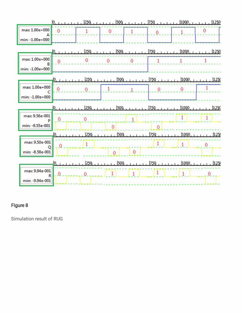
RUG is a 3X3 fault tolerant reversible gate. The three inputs (A, B, C) mapped to the three outputs (P, Q, R).
The block diagram of the RUG is displayed in Figure 5 and its schematic diagram in Figure 6. The QCA
realization of the RUG is as seen in Figure 7. Figure 8 depicts its simulation result.
Insert Fig. 5
Insert Fig. 6
Insert Fig. 7
Insert Fig.8
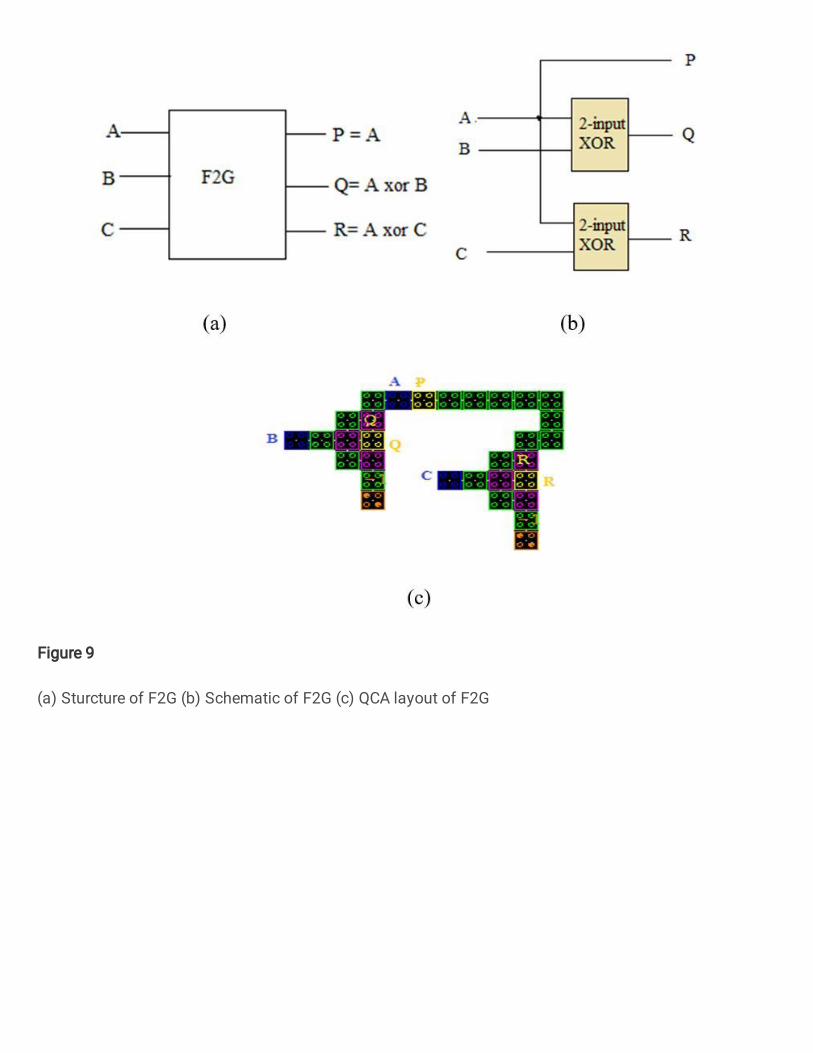
2.F2G
Double Feynman gate(F2G) is a 3X3 fault tolerant reversible gate. The block diagram of the F2G and its
corresponding schematic diagram is as depicted in Figure 9.a & b. The QCA realization of the F2G is as
displayed in Figure 9..c. Figure 10 shows the simulation result of the F2G gate.
Insert Fig. 9
Insert Fig.10
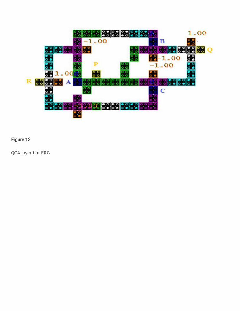
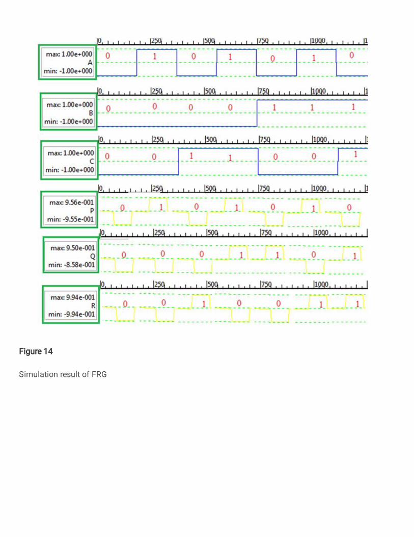
3.FRG
Fredkin gate(FRG) is a 3X3 fault tolerant reversible gate. The block diagram of the FRG is as seen in Figure 11
and its corresponding schematic diagram in Figure 12. The QCA realization of the FRG is as presented in
Figure 13 and its simulation output in Figure 14.
Insert Fig. 11
Insert Fig. 12
Insert Fig. 13
Insert Fig.14
4.FG
Feynman gate(FG) is a 2X2 reversible gate. The block diagram of the FG and its corresponding schematic
diagram is as seen in Figure 15. The QCA realization and simulation result of the FG are displayed in Figures
16 and 17.
Insert Fig. 15
Insert Fig. 16
Insert Fig.17
5.UPPG
Universal parity preserving gate(UPPG) is a 4X4 reversible gate. The structure of the UPPG is as seen in Figure
18 and its corresponding schematic diagram in Figure 19. The QCA realization and simulation result of the
UPPG is as presented in Figure 20 and 21 respectively.
5
Insert Fig. 18
Insert Fig. 19
Insert Fig. 20
Insert Fig.21
3.Related work
Different approaches have been implemented in recent years to enhance the performance of elements of the ALU.
There are, however, only a few architectures suggested for designing QCA ALU. The authors have suggested a 4-bit
QCA ALU in [3]. This approach uses three layers, 420 QCA cells, latency in three clock zones, and an area of 0.85
μm2. This layout is not using the fault-tolerant reversible gates as well as it is using more number of QCA cells to
implement. The authors suggested a method to implement QCA ALU capable of performing 12 logic and arithmetic
operations[4]. But, this approach uses 485 QCA cells, an area of 0.79 μm2, and latency of five clock zones. There are many drawbacks to this process, as the absence of reversibility, exclusion of fault tolerance, high consumption of
cells, and also high latency. Trailokya Nath Sasamal et al.[5] designed a reversible ALU in QCA using the coplanar
crossing. But the proposed design uses more number of QCA cells and performs only 20 ALU operations only. In
[13], the authors constructed a reversible QCA ALU using a reversible MUX. However, the design is able to
perform only 16 operations with more number of constant inputs and garbage outputs. Sasamal et al.[14] propose a
QCA ALU using reversible logic. They considered a 3X3 RUG fault tolerant reversible gate as a fundamental
element in synthesizing reversible ALU design. But it can perform only 16 ALU operations only. The authors [15]
propose an integrated fault-tolerant QCA ALU using KMD reversible gates. The suggested design can be able to
perform only 18 operations with an increased number of constant inputs, gates, and garbage outputs.
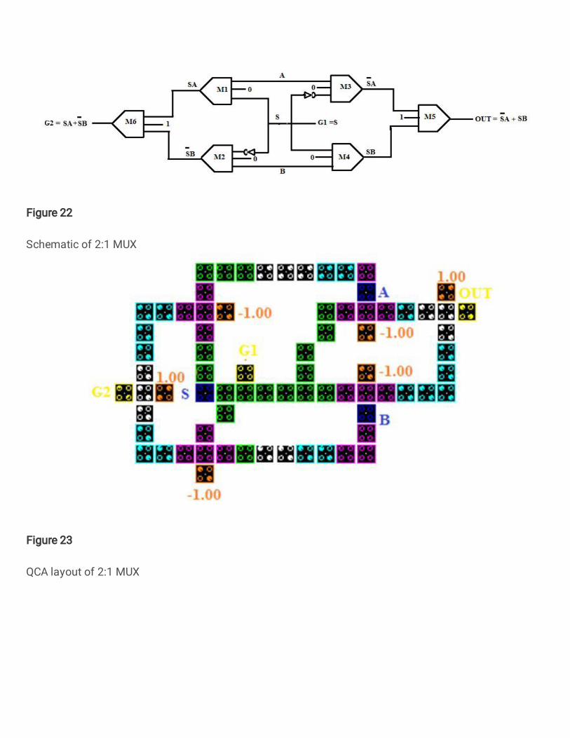
4. Reversible MUX and full adder
4.1 Reversible MUX
Using Fredkin's reversible logic gate, a novel 2:1 MUX has been constructed in QCA technology. All the potential
benefits with this proposed new multiplexer seem to be reversible logic that is not present in the traditional MUX.
One of the crucial characteristics in designing the logic circuit using reversible gates is to reduce the count of
reversible gates and garbage outputs. The schematic diagram of the proposed MUX is as shown in Figure 22 and its
QCA layout in Figure 23. The designed circuit utilizes only 75 QCA cells, only one gate, and an area of 0.08µm2.
Figure 24 depicts the simulation result of the suggested 2:1 MUX.
Insert Fig. 22
Insert Fig. 23
Insert Fig.24
4.2 Full adder
The proposed reversible fault tolerant full adder circuit is designed using RUG and F2G gates. The schematic
diagram and QCA layout of the suggested circuit is as shown in Figure 25 and 26 respectively. It utilizes a very less
cell count of 107 QCA cells compared to its earlier designs. The circuit is said to be fault-tolerant and less are
utilization as it is implemented with the parity preserving reversible gates RUG and F2G. The simulation result of
the suggested full adder is depicted in figure 27.
6
Insert Fig. 25
Insert Fig. 26
Insert Fig.27
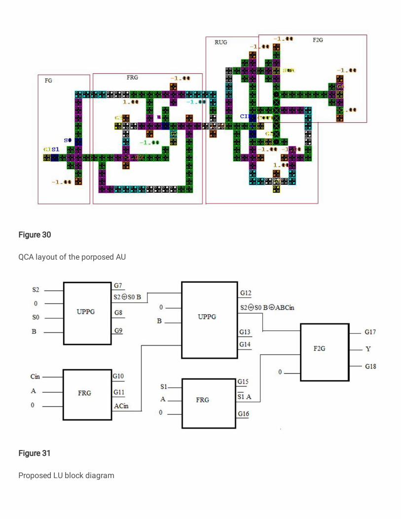
5. Proposed fault tolerant reversible ALU
An arithmetic and logic unit is an essential part of several computing systems. With minimal hardware cost, the
desired requirement of an ALU should execute the maximum allowable operations. The suggested fault tolerant
reversible ALU unit has separated into two sub-components: (1) a reversible arithmetic unit (AU)(2) a logic
unit(LU), which is shown in Figure 28. The signals used for this ALU are A, B & Cin(three inputs), constant inputs,
and selection lines (S0, S1 & S2). A 2X1 MUX is used to choose an output from any of the two components.
Insert Fig. 28
5.1 Arithmetic Unit
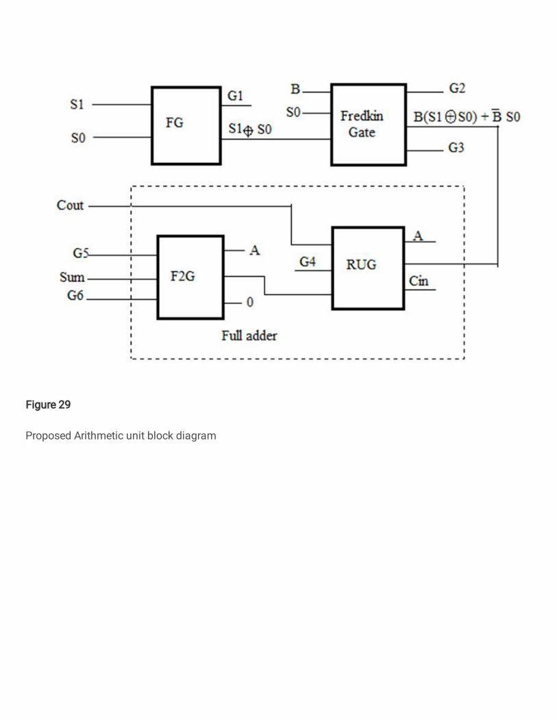
The reversible fault tolerant arithmetic unit (RAU) using the suggested full adder is seen in Figure 29. It
incorporates one gate of FG, Fredkin, RUG, and F2G. It performs eight arithmetic operations like transfer,
increment, decrement, copy, addition without carrying input, addition with carrying input, and addition with
complement as depicted in Table 1. The reversible arithmetic module has five inputs (A, B, Cin, S0 & S1), two
actual outputs(sum & Cout), and six garbage outputs (G1, G2, G3, G4, G5 & G6). The expressions for the two
outputs sum and Cout are given by the following equations 5 & 6. The synthesized QCA layout of the suggested


![A novel transmission line relaying scheme for fault ... · of fault in [12].In[13] phase space based fault detection scheme for distance relaying is proposed. Fault classification](https://static.documents.pub/doc/80x56/6049f3c4320dff2310093181/a-novel-transmission-line-relaying-scheme-for-fault-of-fault-in-12in13.jpg)


