Page 1
European Scientific Journal May 2017 edition Vol.13, No.15 ISSN: 1857 – 7881 (Print) e - ISSN 1857- 7431
254
A Novel Design and Implementation of 8-3 Encoder
Using Quantum-dot Cellular Automata (QCA)
Technology
Md. Sofeoul-Al-Mamun
Mohammad Badrul Alam Miah
Fuyad Al Masud Department of Information and Communication Technology (ICT), Mawlana
Bhashani Science and Technology University, Tangail, Bangladesh
doi: 10.19044/esj.2017.v13n15p254 URL:http://dx.doi.org/10.19044/esj.2017.v13n15p254
Abstract In recent years Quantum-dot Cellular Automata (QCA) has been
considered one of the emerging nano-technology for future generation digital
circuits and systems. QCA technology is a promising alternative to
Complementary Metal Oxide Semiconductor (CMOS) technology. Thus,
QCA offers a novel electronics paradigm for information processing and
communication system. It has attractive features such as faster speed, higher
scale integration, higher switching frequency, smaller size and low power
consumption compared to the transistor based technology. It is projected as a
promising nanotechnology for future Integrated Circuits (ICs). A quantum
dot cellular automaton complex gate is composed from simple 3-input
majority gate. In this paper, a 8-3 encoder circuit is proposed based on QCA
logic gates: the 4-input Majority Voter (MV) OR gate. This 7-input gate can
be configured into many useful gate structures such as a 4-input AND gate, a
4-input OR gate, 2-input AND and 2-input OR gates, 2-input complex gates,
multi-input complex gates. The proposed circuit has a promising future in the
area of nano-computing information processing system and can be
stimulated with higher digital applications in QCA.
Keywords: Quantum-dot Cellular Automata (QCA), Majority Voter (MV)
Gate, QCA Logic Gates, QCA Designer, 8-3 Encoder Circuit
Introduction
Application of quantum technology in various fields is increasing day
by day (Lent et al. 1993). In course of such a trend quantum-dot cellular
automata are getting projected as a promising nanotechnology for future ICs
(Lent, C. S., 1997). Recently, reversible (Bahar, et al., 2013; Sarker, et al.,
Page 2
European Scientific Journal May 2017 edition Vol.13, No.15 ISSN: 1857 – 7881 (Print) e - ISSN 1857- 7431
255
2014; Islam, et al. 2014 ; Shafi, et al. 2015; Islam, et al. 2016 ; Al-Shafi, et
al. 2016) and ( Abdullah-Al-Shafi, M., 2016) circuits have been implemented
in QCA by the researchers successfully. A QCA is an array of structures
known as quantum-dots. Computing with QCA is achieved by the tunneling
of individual electrons among the quantum-dots inside a cell and the
classical coulombic interaction among them. A quantum cell can be viewed
as a set of four charge containers or dots positioned at the corners of a
square, as shown in Fig. 1. It contains two extra mobile electrons. The
electrons can quantum mechanically tunnel between dots but cannot come
out from the cell and are forced to settle at the corner positions due to
coulomb interaction. Thus, there exist two equivalent energetically minimal
arrangements for the electrons in a QCA cell.
In Fig. 1, a QCA cell and its binary logic are shown. The
energetically position of the diagonal electrons identify the binary logic 0 or
1. This phenomenon is useful in nanotechnology which affects high
resolution fast electronic circuits.
Fig.1. A QCA cell and its binary logic, (a) Structure of a QCA cell, (b) Representing a
binary digit with the help of 2 different polarizations of the localized electron
QCA Wires
The QCA cells themselves comprise the interconnecting wires (Lent
et al. 1993). QCA cells are described in (Niemier, M. T., A. F. Rodrigues and
P. M. Kogge., 2002) . An example of a QCA wire is shown in Figure 2. In
this example, a value of 1 is transmitted along the wire. Only a slight
polarization in a cell is required to fully polarize its neighbor. The direction
for the flow of information through a gate or a wire is controlled by a four
stage clocking system which raises and lowers barriers between the cells
(Lent, C. S., et al 1997).
Page 3
European Scientific Journal May 2017 edition Vol.13, No.15 ISSN: 1857 – 7881 (Print) e - ISSN 1857- 7431
256
Fig. 2. QCA wire
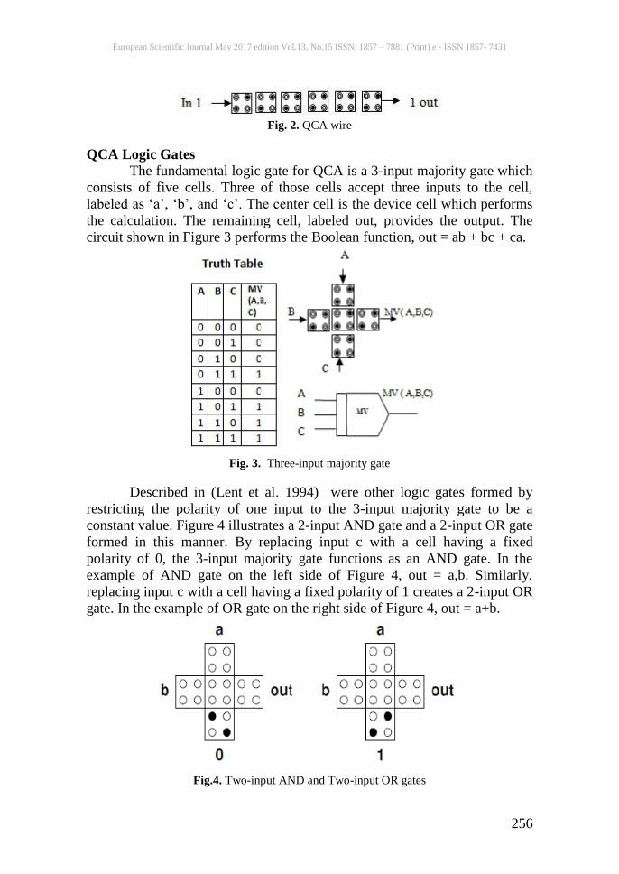
QCA Logic Gates The fundamental logic gate for QCA is a 3-input majority gate which
consists of five cells. Three of those cells accept three inputs to the cell,
labeled as ‘a’, ‘b’, and ‘c’. The center cell is the device cell which performs
the calculation. The remaining cell, labeled out, provides the output. The
circuit shown in Figure 3 performs the Boolean function, out = ab + bc + ca.
Fig. 3. Three-input majority gate
Described in (Lent et al. 1994) were other logic gates formed by
restricting the polarity of one input to the 3-input majority gate to be a
constant value. Figure 4 illustrates a 2-input AND gate and a 2-input OR gate
formed in this manner. By replacing input c with a cell having a fixed
polarity of 0, the 3-input majority gate functions as an AND gate. In the
example of AND gate on the left side of Figure 4, out = a,b. Similarly,
replacing input c with a cell having a fixed polarity of 1 creates a 2-input OR
gate. In the example of OR gate on the right side of Figure 4, out = a+b.
Fig.4. Two-input AND and Two-input OR gates
Page 4
European Scientific Journal May 2017 edition Vol.13, No.15 ISSN: 1857 – 7881 (Print) e - ISSN 1857- 7431
257
Input Complex Gates
Despite that the fundamental logic structure of QCA is the 3-input
majority gate, many of the attempts to implement functional circuitry using
these majority gates begin by restricting them to a subset of their full
information content potential. Previous complex gates, requiring more than
one device cell are described in the literature; however these complex gates
are still restricted to implementing 2- input functions. In (Niemier, M. T., A.
F. Rodrigues and P. M. Kogge., 2002) a complex gate is used to implement a
2-input XOR function (Bahar, et al. 2017). In (Bahniman et al. 2013) a 3-
input majority gate restricted to an AND gate configuration (similar to that
shown in Figure 4) followed by an inverter was used to form 2-input NAND
building blocks for an FPGA implementation. An alternative to this approach
however, is to use the 3-input majority gate as a building block to build even
larger and more complex gate components containing multiple control and
information inputs.
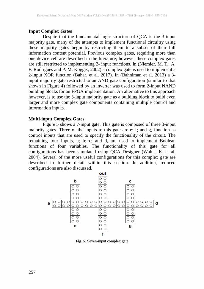
Multi-input Complex Gates
Figure 5 shows a 7-input gate. This gate is composed of three 3-input
majority gates. Three of the inputs to this gate are e; f; and g, function as
control inputs that are used to specify the functionality of the circuit. The
remaining four Inputs, a; b; c; and d, are used to implement Boolean
functions of four variables. The functionality of this gate for all
configurations has been simulated using QCA Designer (Walus, K. et al.
2004). Several of the more useful configurations for this complex gate are
described in further detail within this section. In addition, reduced
configurations are also discussed.
Fig. 5. Seven-input complex gate
Page 5
European Scientific Journal May 2017 edition Vol.13, No.15 ISSN: 1857 – 7881 (Print) e - ISSN 1857- 7431
258
Four-Input AND Gates
The 7-input gate of Figure 5 can be used to form a 4- input AND gate
as shown in Figure 6 by restricting inputs 'e', 'f' and 'g' to have a fixed
polarity that is equal to 0. Although the selection of 'f' is unique, either 'a' or
'b' can be restricted rather than 'e' and similarly 'c' or 'd' can be selected for
restriction rather than 'g'. For the example of circuit as shown in Figure 6, the
function represented is out = a,b,c,d.
Fig. 6. Four-input AND gate
Four-Input OR Gates
Similarly, the 7-input gate of Figure 5 can also be used to form a 4-
input OR gate. For this configuration the inputs 'e', 'f' and 'g' are restricted to
have a fixed polarity that is equal to 1. As for the AND gate, the selection of
'f' is unique. For the remaining two fixed polarity cells, the same symmetry is
presented in the OR gate as in previously described AND gate, either 'a' or 'b'
can be restricted rather than 'e' and likewise 'c' or 'd' can be selected for
restriction rather than g. The function represented is out = a + b + c + d.
Proposed 8-3 Encoder
In Traditional 8-3 encoder logic diagram is presented in Fig. 7.
Fig. 7. Traditional 8-3 encoder logic diagram
Page 6
European Scientific Journal May 2017 edition Vol.13, No.15 ISSN: 1857 – 7881 (Print) e - ISSN 1857- 7431
259
The block diagram of QCA is the 8-3 encoder shown in Figure 8.
Fig. 8. Block Diagram of QCA is the 8-3 encoder.
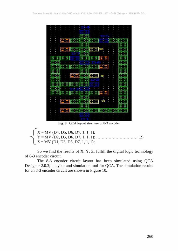
The fundamental logic gate for QCA is the 8-3 encoder shown in
Figure 9 that is composed of Seventy Nine (79) cells. In general, an 8-3
encoder has an output expression as is shown in Eq. (1) where D1, D2, D3, D4,
D5, D6, and D7 are the seven inputs.
X= D4, D5, D6, D7;
Y= D2, D3, D6, D7; ………………………………… (1)
Z= D1, D3, D5, D7;
In Fig. 9, when the binary signals (0 and 1) are inputted into the 8-3
encoder circuit, the input digits (D1 , D2, D3, D4, D5, D6, D7) are decoded to the
decimal digits(X, Y, Z). According to the logic computation in Fig. 9, we can
represent this logic expressions based on the majority gates as shown in Eq.
(2).
Page 7
European Scientific Journal May 2017 edition Vol.13, No.15 ISSN: 1857 – 7881 (Print) e - ISSN 1857- 7431
260
Fig. 9 QCA layout structure of 8-3 encoder
X = MV (D4, D5, D6, D7, 1, 1, 1);
Y = MV (D2, D3, D6, D7, 1, 1, 1); ………………………… (2)
Z = MV (D1, D3, D5, D7, 1, 1, 1);
So we find the results of X, Y, Z, fulfill the digital logic technology
of 8-3 encoder circuit.
The 8-3 encoder circuit layout has been simulated using QCA
Designer 2.0.3; a layout and simulation tool for QCA. The simulation results
for an 8-3 encoder circuit are shown in Figure 10.
Page 8
European Scientific Journal May 2017 edition Vol.13, No.15 ISSN: 1857 – 7881 (Print) e - ISSN 1857- 7431
261
Fig.10 Simulated waveforms for 8-3 encoder circuit
In this Simulation we used the coherence vector computational
engine and the following parameters: 10nm × 10nm cell size, 2.5nm cell-to-
cell distance, and 2.5 dot size and 40nm radius of influence. Table 1 Comparison of proposed designs
Design Number of cells Area (in μm2) Delay
8-3 bit simple encoder
Bahar, A. N. 281 0.22 × 0.30 = 0.06 2.25
Proposed 8-3 bit simple
encoder 79 0.32 × 0.42 = 0.13 1.25
Page 9
European Scientific Journal May 2017 edition Vol.13, No.15 ISSN: 1857 – 7881 (Print) e - ISSN 1857- 7431
262
Conclusions
This paper presents an 8-3 encoder that consists of 7-input majority
gate. Three of these inputs typically function as control inputs to determine
the Boolean function formed by the four other inputs to the circuit. This 7-
input gate can be configured as a 4-input OR gate, a product of sums
representation, a sum of products representation, and other variations. This
QCA circuit design provides a new functional paradigm for information
encoding. In addition, QCA binary logic functions and the associated new
nano-technology will provide high-speed computing, high-density
applications. It is believed that QCA will become a more practical way to
create a faster and denser circuit. All designs are carefully clocked and
functionally verified using QCAdesigner. Finally, in Table 1, designs are
compared in terms of number of cells, area and delay.
References: 1. Lent, C. S. and P. D Tougaw (1993). Lines of interacting quantum-
dot cells: A binary wire, Journal of Applied Physics, 74(10): 6227-
6233.
2. Lent, C. S., P. D. Tougaw and W. Porod (1993). Bistable saturation
in coup- led quantum dots for quantum cellular automata, Applied
Physics Letters, 62 (7): 714-716.
3. Lent, C. S., P. D. Tougaw and W. Prod (1994). Quantum Cellular
Automata: The physics of computing with quantum dot molecules,
Physics and Comput-ation, pp. 5–13.
4. Lent, C. and P. Tougaw (1997). A device architecture for computing
with quantum dots, Proceedings of the IEEE, 85: 541 – 557.
5. Niemier, M. T., A. F. Rodrigues and P. M. Kogge (2002), .A
potentially impl-ementable FPGA for quantum dot cellular automata,.
in 1st Workshop on Non-Silicon Computation, Cambridge, MA,
February 3, pp.38-45.
6. Walus, K., Dysart, T. J., Jullien, G. A., & Budiman, R. A. (2004).
QCADesigner: a rapid design and Simulation tool for quantum-dot
cellular automata. IEEE Transactions on Nanotechnology, 3(1), 26–
31. https://doi.org/10.1109/TNANO.2003.82081
7. Liu, Y. (2008). Modified Quantum Genetic Algorithm Apply for
Flow Shop SchedulingProblem, JCIS, 4: 183 – 188.
8. Li, H., S. Li (2011). A Quantum Immune Evolutionary Algorithm
and Its Application, Journal of Computational Information Systems,
7: 2972 – 2979.
9. Bahar, A. N., Waheed, S., Uddin, M. A., & Habib, M. A. (2013).
Double Fey-nman gate (F2G) in Quantum- dot Cellular Automata
Page 10
European Scientific Journal May 2017 edition Vol.13, No.15 ISSN: 1857 – 7881 (Print) e - ISSN 1857- 7431
263
(QCA). International Journal of Computer Science Engineering,
2(6), 351–355.
10. Bahar, A. N., Habib, M. A., & Biswas, N. K. (2013). A Novel
Presentation of Toffoli Gate in Quantum-dot Cellular Automata
(QCA). International Journal of Computer Applications, 82(10), 1–4.
11. Bahniman Ghosh and Shoubhik Gupta (2013). Novel design of
combinationa-l and sequential logical structures in quantum dot
cellular automata, Journal of Nanostructure in Chemistry (Springer
Open), 3:15 doi:10.1186/2193-886 5-3-15.
12. Sarker, A., Bahar, A. N., Biswas, P. K., & Morshed, M. (2014). A
novel pres-entation of Peres gate (PG) in quantum-dot cellular
automata (QCA). Euro -pean Scientific Journal, 10(21), 101–106.
13. Rahman, A., Habib, M. A., Bahar, A. N., & Rahman, Z. (2014).
Novel desig-n of BCD to Excess-3 code converter in Quantum Dots
Cellular Automata (QCA). Global Journal of Research In
Engineering, 14(4), 7–12.
14. Bahar, A. N., Waheed, S., & Habib, M. A. (2014). A novel
presentation of reversible logic gate in Quantum-dot Cellular
Automata (QCA). In 2014 Inte- rnational Conference on Electrical
Engineering and Information Communi-cation Technology
(ICEEICT) (pp. 1–6).
15. Islam, S. S., Farzana, S., & Bahar, A. N. (2014). Area efficient layout
design of Multiply Complements Logic (MCL) gate using QCA
technology. Global Journal of Research In Engineering, 14(4).
16. Bahar, A. N., Waheed, S., & Habib, M. A. (2015). An efficient layout
design of fredkin gate in quantum-dot cellular automata (QCA).
Düzce Üniversitesi Bilim ve Teknoloji Dergisi, 3(1), 219–225.
17. Bahar, A. N., Waheed, S., & Hossain, N. (2015). A new approach of
present-ng reversible logic gate in nanoscale. SpringerPlus, 4(1).
18. Abdullah-Al-Shafi, M., Islam, M. S., & Bahar, A. N. (2015). A
review on reversible logic gates and its QCA implementation.
International Journal of Computer Applications, 128(2), 27–34.
19. Shafi, A. A., Bahar, A. N., & Islam, M. S. (2015). A quantitative
approach of reversible logic gates in QCA. Journal of
Communications Technology, Electronics and Computer Science,
3(0), 22–26.
20. Islam, M. S., Shafi, M. A.-A., & Bahar, A. N. (2015).
Implementation of binary to gray code converters in Quantum Dot
Cellular Automata. Journal of Today’s Ideas– Tomorrow’s
Technologies, 3(2), 145–160.
https://doi.org/10.15415/jotitt.2015.32010
Page 11
European Scientific Journal May 2017 edition Vol.13, No.15 ISSN: 1857 – 7881 (Print) e - ISSN 1857- 7431
264
21. Abdullah-Al-Shafi, M., & Bahar, A. N. (2016). QCA: An effective
approach to implement logic circuit in nanoscale. In 2016 5th
International Conferenc-e on Informatics, Electronics and Vision
(ICIEV) (pp. 620–624). https://doi.org/10.1109/ICIEV.2016.7760076
22. Bahar, A. N., & Waheed, S. (2016). Design and implementation of an
efficie-nt single layer five input majority voter gate in quantum-dot
cellular automa -ta. SpringerPlus, 5(1).
https://doi.org/10.1186/s40064-016-2220-7
23. Al-Shafi, A., & Bahar, A. N. (2016). Novel binary to gray code
converters in QCA with power dissipation analysis. International
Journal of Multimedia and Ubiquitous Engineering, 11(8), 379–396.
https://doi.org/10.14257/ijmue.2016.11.8.38
24. Abdullah-Al-Shafi, M., & Bahar, A. N. (2016). Optimized design and
perfor-mance analysis of novel comparator and full adder in
nanoscale. Cogent En-gineering, 3(1).
https://doi.org/10.1080/23311916.2016.1237864
25. Islam, M. S., Abdullah-Al-Shafi, M., & Bahar, A. N.(2016). A new
approach of presenting Universal Reversible Gate in nanoscale.
International Journal of Computer Applications, 134(7), 1–4.
26. Bahar, A.N., Rahman, M. M., Nahid, N.M., & Hassan, M. K. (2017).
Energy dissipation dataset for reversible logic gates in quantum dot-
cellular automat-a. Data in Brief, 10, 557–560.
https://doi.org/10.1016/j.dib.2016.12.050