A NOVEL DSP-BASED SWITCH MODE POWER SUPPLY REDUCES OVERALL PARTS COUNT WHEN COMPARED TO AN ANALOG IC BASED APPROACH. Abstract Digital Signal Processors (DSP’s) have come to dominate designs that previously used analog solutions. Power electronics remains a bastion for Analog IC’s, largely because of the simple “1 bit” A/D process offered by peak current control. This simple control concept combined with control system bandwidth extending to hundreds of kilohertz has kept the digital genie bottled. But with Moore’s law heaping additional millions of transistors on the pile each year at ever lower prices; the digital solution will ultimately prevail. Cost remains the near-term bottleneck but bandwidth can easily handle the problem for switching rates in the hundreds of kilohertz range. As a rule of thumb, execution of 100 or 200 instructions per sample is the threshold for a DSP solution. The DSP sample rate can be as fast as the Pulse Width Modulator (PWM) switching frequency; so that 30 Million Instructions Per Second (MIPS) is adequate for a 100kHz, Switch Mode Power Supply (SMPS). Coincidently, an idle process can be added to solve the myriad of problems peculiar to a specific design. The designer is no longer limited to the fixed algorithms incorporated in SMPS Integrated Circuits (IC’s). The technique presented here will actually minimize the total parts count of a hypothetical DSP design. Summary First, the tools needed to apply power supply control system design techniques to DSP technology will be reviewed. These basic concepts include stability analysis and predicting transient behavior using SPICE simulation. Then a novel design concept will be introduced that can take advantage of using a DSP. While using a DSP isn’t necessary to this solution, the complexity of an analog solution wouldn’t otherwise be competitive with state of the art peak current control IC’s. A plant model, similar to that used for Kalman filters exposes current as a “hidden” parameter, thus eliminating the need for sensing current. The concept will be shown as viable using a SPICE simulation. Then the s-plane operations in SPICE will be converted into a z-transform solution. Finally the DSP difference equations will be derived, and a DSP reference design will be completed and tested for a simple buck regulator. Z Transform Basics Design and analysis of control systems are usually performed in the frequency domain; whereby the time domain process of convolution is replaced by a simple process of multiplication of complex polynomials in the frequency domain. Sampled data systems use a similar concept using a unit delay as the basic building block. The analog s-plane maps into the sampled data z-plane by substitution of variables where z=e sT or more importantly by z -1 =e -sT The later representation is seen to be identical to a delay line, with z -n representing a delay of nT seconds. Transfer functions, including impedance and admittance functions are described as polynomial ratios of the form G=N/D, where N=a 0 + a 1 z -1 + … a n z -n and D = 1 + b 1 z -1 + … + b n z -n are the numerator and denominator polynomials respectively. Notice that b 0 = 1. Then rearranging the following equation with D’ = D-1 Vo/Vi = N/D Vo(1+D’) = ViN Vo = ViN-VoD’ This is the “Direct” programming method that is more rigorously derived in [1] pp
Transcript
A NOVEL DSP-BASED SWITCH MODE POWER SUPPLY REDUCES OVERALL PARTS COUNT WHEN COMPARED TO AN ANALOG IC BASED APPROACH. Abstract Digital Signal Processors (DSP’s) have come to dominate designs that previously used analog solutions. Power electronics remains a bastion for Analog IC’s, largely because of the simple “1 bit” A/D process offered by peak current control. This simple control concept combined with control system bandwidth extending to hundreds of kilohertz has kept the digital genie bottled. But with Moore’s law heaping additional millions of transistors on the pile each year at ever lower prices; the digital solution will ultimately prevail. Cost remains the near-term bottleneck but bandwidth can easily handle the problem for switching rates in the hundreds of kilohertz range. As a rule of thumb, execution of 100 or 200 instructions per sample is the threshold for a DSP solution. The DSP sample rate can be as fast as the Pulse Width Modulator (PWM) switching frequency; so that 30 Million Instructions Per Second (MIPS) is adequate for a 100kHz, Switch Mode Power Supply (SMPS). Coincidently, an idle process can be added to solve the myriad of problems peculiar to a specific design. The designer is no longer limited to the fixed algorithms incorporated in SMPS Integrated Circuits (IC’s). The technique presented here will actually minimize the total parts count of a hypothetical DSP design. Summary First, the tools needed to apply power supply control system design techniques to DSP technology will be reviewed. These basic concepts include stability analysis and predicting transient behavior using SPICE simulation. Then a novel design concept will be introduced that can take advantage of using a DSP. While using a DSP isn’t necessary to this solution, the complexity of an analog solution wouldn’t otherwise be competitive with state of the art peak current control IC’s. A plant model, similar to that used for Kalman filters exposes current as a “hidden” parameter, thus eliminating the need for sensing current. The concept will be shown as viable using a SPICE simulation. Then the s-plane operations in SPICE will be converted into a z-transform solution. Finally the DSP difference equations will be derived, and a DSP reference design will be completed and tested for a simple buck regulator. Z Transform Basics Design and analysis of control systems are usually performed in the frequency domain; whereby the time domain process of convolution is replaced by a simple process of multiplication of complex polynomials in the frequency domain. Sampled data systems use a similar concept using a unit delay as the basic building block. The analog s-plane maps into the sampled data z-plane by substitution of variables where z=esT or more importantly by
z-1=e-sT
The later representation is seen to be identical to a delay line, with z-n representing a delay of nT seconds. Transfer functions, including impedance and admittance functions are described as polynomial ratios of the form G=N/D, where N=a0 + a1z-1 + … anz-n and D = 1 + b1z-1 + … + bnz-n are the numerator and denominator polynomials respectively. Notice that b0 = 1. Then rearranging the following equation with D’ = D-1 Vo/Vi = N/D Vo(1+D’) = ViN Vo = ViN-VoD’ This is the “Direct” programming method that is more rigorously derived in [1] pp
475,477. This equation can also be implemented in the s-plane using the following block diagram with the unit time delay (UTD) replaced by a SPICE transmission line. This implementation allows for SPICE analysis of the time domain difference equations, including both transient and ac analysis, and of course Bode plots.
SUM2
K1
K2
2
18
4
K1 = a1K2 = a0
UTD
X3UTD
X1UTD
UTD3
SUM2
K1
K2
K1 = a2K2 = 1
7
X5UTD
z^-1 z^-2 z^-nz^-3UTD
5
SUM2
K1
K2
K1 = anK2 = 1
8
6
1
. . .
. . .
UTD109
X8UTD
UTD12
X9UTD
SUM2
K1
K2
K1 = b2K2 = 1
11
13
UTD14
X11UTD
z^-1z^-2z^-n z^-3
SUM2
K1
K2
K1 = bnK2 = 1
15
16
19
. . .
. . .
SUM2
K1
K2
K1 = 1K2 = -1
Vi
Numerator
Denominator
Vo
GAIN
K = b1
Figure z1, Direct Programming Method Bilinear Transform Solving for s as a function of z yields
)ln(1 zT
s =
The ln(z) function can be broken down into 3 common approximations. Lets first do this by using the first term of the series expansion
where 112)ln(
+−
=zzz
Then for ,/1 Tw << zz 21≈+ to further simplify to
zzz 1)ln( −
= so that
or as w approaches infinity, z approaches zero and ln(z) = z-1 Then, the 3 approximations are:
( )11−= z
Ts
⎟⎠⎞
⎜⎝⎛ −
=z
zT
s 11
⎟⎠⎞
⎜⎝⎛
+−
=11
21
zz
Ts
The second representation is the one commonly used [1] pg 471 in the z-transform tables. Mathematically it is common to let T = 1 and omit it from the tables, leaving it to the user to scale the result for other sample frequencies. If you fail to account for T, then you will get the wrong answer! Restating the above equations to represent integration and delays yields:
⎟⎟⎠
⎞⎜⎜⎝
⎛−
= −
−
1
1
11
zzT
s Rectangular, backward Euler, integration eq 1
⎟⎟⎠
⎞⎜⎜⎝
⎛−
= −1111z
Ts
Rectangular, forward Euler, integration eq 2
(z Transform)
⎟⎟⎠
⎞⎜⎜⎝
⎛−+
= −
−
1
1
11
21
zzT
s Trapezoidal integration eq 3
(Bilinear transform) There are 3 interpretations to these equations in terms of integration method, although they were derived here from a series expansion; they could have also been derived in time domain using rectangular and trapezoidal integration methods. These representations have several interesting properties. First, eq 1, has a step response of z-1, which is interpreted as the dead-beat response, that is, the error to a step response will be reduced to zero in one sample time. That’s the holy grail of digital control system design, so the loop compensation should be designed to replicate that behavior. Unfortunately, adding 6dB of gain makes it unstable. The second equation gives really good results for control system compensation as shown if figure z2, the phase is leading near the nyquist frequency, providing added margin. Finally, eq 3 inserts a term that averages the previous sample with the current sample.
The average of 2 samples at ½ the nyquist frequency is exactly zero for any signal, at Fs/2, regardless of its phase. Figure z3 shows this result and also shows that phase stays at 90 degrees up to Fs/2. Both figures represent current through 100uHy at Fs=100kHz.
1 ph_is 2 db_is 3 ph_iz 4 db_iz
10k 20k 50k 100kfrequency in hertz
-50.0
50.0
150
250
3501324
db_i
z, d
b_is
in d
B
-80.0
-40.0
0
40.0
80.0
ph_i
z, p
h_is
in d
egre
esP
lot1
s-plane phase
z-plane phase
s plane magnitude
z-plane magnitude
Figure z2, Z Transform of an integrator compared with continuous time integration
1 ph_is 2 db_is 3 ph_izb 4 db_izb
10k 20k 50k 100kfrequency in hertz
-24.0
0
24.0
48.0
72.01324s-plane phase z-plane phase
db_i
zb, d
b_is
in d
B
-120
-60.0
0
60.0
120ph
_izb
, ph_
is in
deg
rees
Plo
t1
s-plane magnitude
z-plane magnitude
Figure z3, Bilinear transform of integrator compared with continuous time integration As frequency increases past ½ the sampling frequency, aliasing causes the results to repeat as shown in figure z4.
Frequency into a switched network
Freq
uenc
y ou
t of a
sw
itche
d ne
twor
k
1/(2T) 1/T
1/(2
T)-1
/(2T)
2/T
Switching Frequency
Figure z4, Time domain frequency out vs. frequency in for sample data systems. While the information bandwidth doesn’t exceed ½ the switching frequency, there is indeed information contained above the sampling frequency. Z-transforms can be used to described heterodyned signal detection by placing an analog bandpass filter about the center frequency of interest followed by a digital lowpass filter. Moreover, the samples can be separated by 90 deg (in time), with the in phase component representing real numbers and the 90 degree delayed sample data being imaginary numbers. A Fourier transform converts the complex time data to the frequency domain where it can be filtered. Then an inverse fourier transform recovers the filtered time dependant data. If certain rules are followed, there will be no imaginary data in the time domain when the inverse transform is taken. Z-Plane Frequency Warping As shown previously in Figures z2 and z3, s-plane poles and zeros ranging to infinity are warped into the z plane. Mathematically, the warping is described by evaluating the s-plane frequency for s = jw and the z-plane frequency = jwz. For the bilinear transform of eq 3:
jw=(2/T)*(e^(jwz*T-1)/( e^(jwz*T+1) Multiplying numerator and denominator by 1/2*e^(-jwz*T/2) gives
w=2/T*sin(wz*T/2)/cos(wz*T/2) w= c *tan(wz*T/2) or wz=2/T*atan(w/c), c=2/T Now, the z-plane argument is phase going from –pi/2 to pi/2 as s-plane frequency goes from – infinity to + infinity.
Figure z5 illustrates this warping. Importantly the warping maps each s-plane frequency to a unique z-plane frequency. Filters such as Chebyshev, Butterworth and Elliptical can be mapped into the z-plane such that filter cutoff frequencies are the same by adjusting c. The filter will then have a somewhat sharper cutoff than its corresponding s-plane filter because frequencies approaching infinity are compressed to ws/2.
1 fz
0 500k 1.00Megf
5.00k
15.0k
25.0k
35.0k
45.0k
fzP
lot1
1
T=10uc=2/Tf = 1k*(1m+vector(1000))fz=2/T*atan(2*pi*f/c)*pi/180/2/piplot fz f
Figure z5, Bilinear transform maps s-plane frequency, f to sampled frequency fz for c=2/T. The script shown in figure z5 was used to plot the graph in the IntuScope waveform viewing tool. Notice that angles are in degrees, while the pi/180 corrects this and frequency is converted from 1/sec to Hertz by scaling w = 2*pi*f. A similar sine based warping occurs using the z-transform method. One additional piece of information is needed in evaluating the two transform options. Sample and Hold Model The digital control system gets its input from an A/D converter that is basically a sample and hold device. Similarly its output is a D/A which is also represented by a sample and hold process. In both cases these are modeled as zero order holds. Consider an input to an A/D with a steady state signal at exactly the sample frequency. It’s obvious that there is no output at the sample frequency because
each sample occurs at exactly the same point on the waveform. Zero order holds are modeled by the transfer function [1] p 56 Gzoh= 1/T*(1-z^-1)/s The transfer function is shown in Figure z6 for a 100kHz sampler.
1 db_v5 2 ph_v5
1k 10k 100k 1Megfrequency in hertz
-48.0
-24.0
0
24.0
48.0
db_v
5 in
db(
volts
)
-420
-300
-180
-60.0
60.0
ph_v
5 in
deg
rees
plot
1
2
1
Figure z6 Zero order hold nulls signals at harmonics of the sampling frequency There is a substantial penalty in the phase lag. Suppose the S&H were followed by a z-transform integrator, G=1/(1-z^-1). Then the net result would be a transfer function of 1/s which is exactly right. So at least when you do your digital computations using the z- transform there isn’t much difference between z and s plane. Moreover, the z-transform is more computationally efficient than the bilinear transform. To Recap; When doing a bilinear transform from continuous to sampled systems, the poles or zeros at infinity move to the nyquist frequency (1/2 the sampling frequency) in the z-plane. For low-pass filters, there are zeros at infinity so that the signals near the nyquist frequency go to zero. The frequency warping between z-plane and s-plane is approximately linear for low frequencies; but s-plane frequencies get compressed near the nyquist frequency and show different behavior depending on the approximation used
for ln(z).The constant c that relates sampled frequency to continuous time frequency can be adjusted to make fz = f at a single frequency. Analog filters are needed to select the appropriate frequency range and are usually low pass, rejecting signals > 1/(2*T). Control systems favor the z transform while filters work better using bilinear transforms. Modeling the Z transform difference equations in the z-domain requires the insertion of zero order holds at the A/D and D/A interface. These analog to digital interface models are part of the controller model and are not included in the DSP equations. Z-transform feedback: Its common to encounter z-transform models with feedback. When we go on to develop the plant model for the R-L-C filter network, the load voltage will be used to calculate the voltage across the inductor, which in turn will be used to compute the load voltage. If eq 2 or eq 3 is used to represent the capacitor impedance and inductor admittance, then this problem occurs and it’s necessary to solve for 2 equations with 2 unknown quantities (capacitor voltage and inductor current). But if one of the equations uses backward Euler integration, eq 1, there is no need to make a matrix solution. Eq 1 adds a time delay to the solution, reducing bandwidth. But without appropriate computer aided design tools, the odds of getting the matrix solution and the DSP coding correct become varnishing small. Problem: Peak current control using the fast 1 bit a/d converter is a good theoretical concept but in practice it’s plagued by noise. The noise is mainly Electro Magnetic Interference (EMI). The EMI is caused by the rapid voltage and current switching of the PWM that excites parasitc ringing at the current sense point.
EMI Sidebar EMI is generally thought of as being capacitively coupled from the PWM switch to the sense resistor. That is the classical electric field coupling. But there is also a magnetic component created by the current loop from the switched current and the input filter capacitor. This field can induce voltages in wiring “loops”; for example a ground loop formed in the so called ground plane. High frequency signals will be forced toward the outside of the ground plane such that the unwanted signals can be picked up by circuits the have their grounds along the circumference of the ground plane. In any event, the ringing at the peak current sense point alters the transfer function, potentially causing control system instabilities that resemble noise.
This EMI at best is chaotic but clearly it is not Gausian. An often-used DSP favorite, the Kalman filter, is a tempting approach; but the poor statistical match may doom its applicability. The Kalman filter uses a plant model to predict the observable state variables and then combines them with the noisy observation to get a “best” estimate. The noise is continuously monitored so the filter adapts to its environment. A common practice in control system design using Kalman filters is to extract “hidden” state variable from the plant model. Assuming the PWM inductor current is a hidden variable; then is it possible to adjust the plant model in a manner that allows extraction of the inductor current? The following approach is postulated:
Apply the measured input voltage and computed duty ratio to the plant model. Add an extra control loop to the plant model, integrating the error difference between plant and measured outputs; and then apply the result to adjust the plant model load current. A block diagram is shown in Figure 1.
Of course, the observed input and output voltage can be filtered using the Kalman technique; but the trick here is to avoid measuring the noisiest variable altogether. That saves a sense resistor and the signal conditioning circuits surrounding the current measurement. Moreover, the analog compensation components are no longer needed; they are folded into the DSP software. But a simple resistor divider signal-conditioning network must be added for each of the 2 voltage measurements. These networks bring the signal range down to the A/D converter measurement range. The relatively heavy signal filtering in the PWM input and output filter act as the DSP anti-aliasing filter so that further analog “noise” filters are unnecessary. The controller itself can use average current or peak current control, borrowing from the SPICE models used to make “average” model PWM controllers. Peak current control requires a division while average control does not. Peak control will have slightly higher bandwidth since it predicts the duty ratio needed to switch the PWM off. Observe that the DC component of current is based on the plant series resistance being the same as the actual sum of inductor resistance and switch resistance; while the high frequency component depends on accurate modeling of the filter inductance. The effect of errors in modeling on stability margins must be considered.
Input Filter Output Filter
z TransformCompensation& Control Law
VoutVin
Duty Ratio
Average PWMOutput Model Output Filter
Model
VoutModel
Load
+
-
DSPLoad Model
Iavg
Block Diagram
Figure 1, Block Diagram Target Design A simplified reference design was chosen. The target problem is for a Buck regulator operating in Continuous Conduction Mode (CCM) with common input and output grounds. This might represent an auxiliary 5 Volt regulator where an off-line SMPS provides the12 Volt source. The principles discussed here should be extensible to
other topologies and to the DCM mode; but issues of measuring input and output voltage when there is a time varying potential between grounds need not be addressed. The DSP output controls Duty ratio directly. The duty ratio is computed based on voltage measurements made near the beginning of a PWM cycle, the average current from the plant model and the estimated charging current. This calculation is a routine part of the many variations of average SPICE models [2], pp153-158. SPICE is capable of modeling continuous time functions by using a variable time step. That capability will be used to make a continuous time analog model. Then the continuous time model will be transformed to a z-transform based model. Finally, the z transform equations are re-arranged into the familiar Infinite Impulse Response (IIR) DSP equations. See intusoft.com/DSP/ControlSidebar.doc For a comparison of pid and current feedback control methods. Performance Investigation: It’s not altogether obvious that the approach outlined if Figure 1 will work. The following objections need to be considered:
1. Is the accuracy of the Iavg model good enough to calculate cycle-by-cycle peak current?
2. What happens if the model and hardware parameter values differ? 3. Is the voltage matching loop stable?
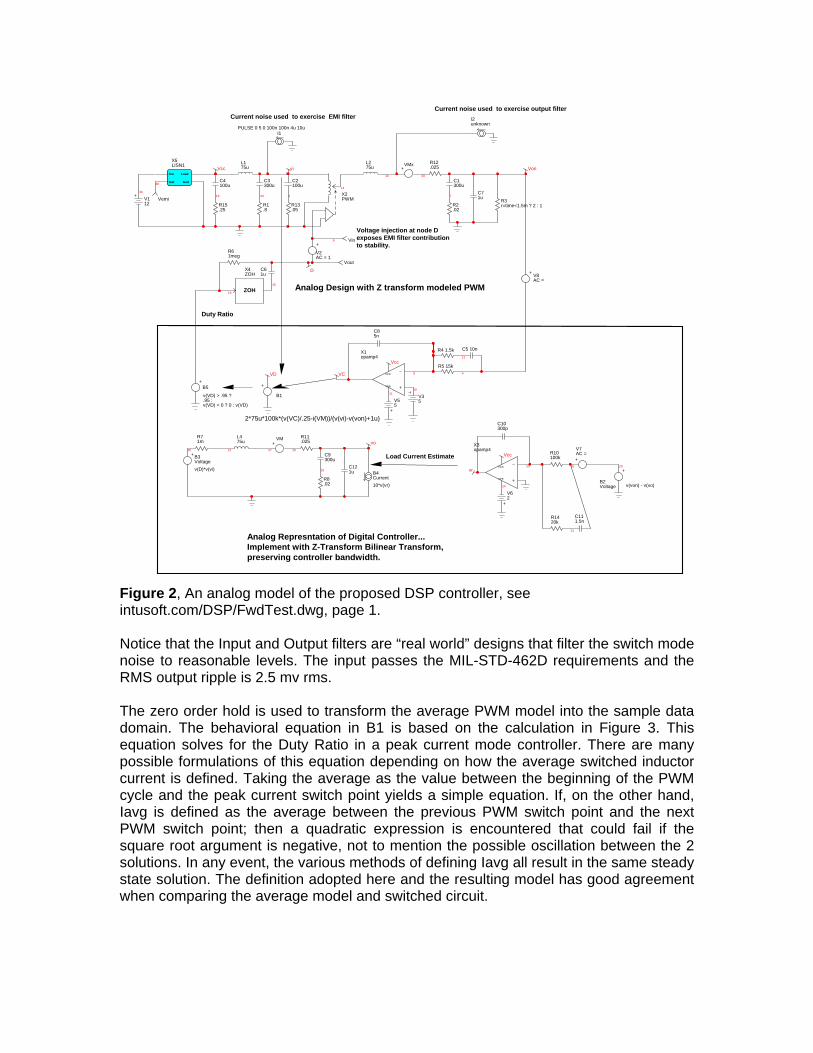
The design shown in Figure 2 was used to investigate theses objections. For this investigation the plant model is in the analog domain.
3
C2100u
36
V112
7
C1300u
R2.02
R3r=time<1.5m ? 2 : 1
VCC
VEE
8
1011
Vcc
X1opamp4
Vcc
9 Vin
Vout
4
R5 15k
V35V5
5
12
R4 1.5k C5 10n
14
X2PWM
16
L275u
B1
2*75u*100k*(v(VC)/.25-i(VM))/(v(vi)-v(von)+1u)
27 25
VM
20
C9300u
R8.02
21
L475u
vi
vo
28
VMx
D
VCC
VEE
23
24
X3opamp4
Vcc
V62
C10300p
26
R10100k
29
B2Voltage
Von
v(von) - v(vo)
vr
R11.025
R12.025
B4Current10*v(vr)
V7AC =
30
B3Voltagev(D)*v(vi)
R71m
31
R1420k
C111.5n
Load Current Estimate
L175u
VC
C85n
34
C3300u
R1.8
R13.05
18
C4100u
R15.25
line
test Gnd
Load
X5LISN1
38
Vemi
V2AC = 1
Current noise used to exercise EMI filter
Voltage injection at node Dexposes EMI filter contributionto stability.
Analog Design with Z transform modeled PWM
Current noise used to exercise output filterI2unknown
PULSE 0 5 0 100n 100n 4u 10u
19
R61meg
35
C61u
ZOH
X4ZOH
B5
v(VD) > .95 ?.95 :v(VD) < 0 ? 0 : v(VD)
VD
I1
Analog Represntation of Digital Controller... Implement with Z-Transform Bilinear Transform,preserving controller bandwidth.
Duty Ratio
C121u
C71u
V8AC =
Figure 2, An analog model of the proposed DSP controller, see intusoft.com/DSP/FwdTest.dwg, page 1. Notice that the Input and Output filters are “real world” designs that filter the switch mode noise to reasonable levels. The input passes the MIL-STD-462D requirements and the RMS output ripple is 2.5 mv rms. The zero order hold is used to transform the average PWM model into the sample data domain. The behavioral equation in B1 is based on the calculation in Figure 3. This equation solves for the Duty Ratio in a peak current mode controller. There are many possible formulations of this equation depending on how the average switched inductor current is defined. Taking the average as the value between the beginning of the PWM cycle and the peak current switch point yields a simple equation. If, on the other hand, Iavg is defined as the average between the previous PWM switch point and the next PWM switch point; then a quadratic expression is encountered that could fail if the square root argument is negative, not to mention the possible oscillation between the 2 solutions. In any event, the various methods of defining Iavg all result in the same steady state solution. The definition adopted here and the resulting model has good agreement when comparing the average model and switched circuit.
Where Vc = Control Voltage Rb = Burden (Sense) Resistor D=Duty Ratio L= Inductance of the switched inductor F=Switching Frequency Figure 3, Plot of current vs. time used to derive peak current control equations Answer to objection 1: A transient simulation was run with the same plant and circuit parameters; the RMS error in estimating Iavg over the entire simulation was 2.6% with the EMI noise injection turned off. Answer to objection 2: Bode Plots for the three control loop cut points taken at V1, V7 and V8 show the typical stability margins in Figure 4,5 and 6. These margins remain acceptable if the circuit inductor is varied from 25uHy to 125uHy with the plant model inductor reaming at 75uHy. The loop cut taken at V1 is not available in hardware because it’s part of the mathematical reconstruction of the current mode control system. This is the inner most loop and it is a powerful tool that can be used to design a stable input filter.
Figure 5, Outer control loop cut at V8 Similarly, other component parameters can be mismatched and the results shown to be stable.
1 phase 2 gain
10 100 1k 10k 100kfrequency in hertz
-24.0
-12.0
0
12.0
24.0
gain
in d
b(vo
lts)
-120
-60.0
0
60.0
120ph
ase
in d
egre
esP
lot1
1
2
L=75uphasemargin = 43.1249 degrees
Figure 6, Plant matching loop cut at V7 Answer to objection 3: Figure 6 shows stability in the voltage matching loop. Scaling; Today’s most cost effective DSP’s use fixed point 16 bit processors. Eventually floating point processors will be available at a low enough cost, however, there will still be scaling issues that can borrow from the fixed point technology. From the microprocessor unit (MPU) point of view, digital filters consist of taking sums of products. If the binary point is placed to the left side of the digital word, the result is interpreted as a fraction. Multiplication of 16 bit fractions produce a 32 bit result, but the lower 16 bits can be rounded into the upper 16 bit word and discarded. There will be no numerical overflow resulting from multiplication to consider if fractional scaling is used. The summation can overflow, but if the problem is scaled to prevent overflow of the result, then intermediate overflows will wash out. Consider the two’s compliment world if real numbers are to be mapped onto a circle with positive numbers starting from 0 rotating counterclockwise thru hexadecimal (hex) 7FFF and negative numbers going clockwise thru hex 8001. A Special number, 8000, acts as infinity. Only hex 0000 and hex 8000 2’s compliment back to themselves! When an intermediate overflow occurs, the result continues in the same (CW or CCW) direction. Subsequent summations will unwrap the result back into the original numerical space. However, the z-transform integrator 1/(1-z^-1) could continue on to infinity if its output is not limited
But the plot thickens when the DSP accumulator has extra high order bits with saturation logic. That allows for intermediate overflow because of the extra precision. Then it become convenient to scale the problem to an x.y space, where x are integer bits and y are fraction bits (x+y=16). Then after each multiply accumulate operation is finished, the result must be shifted into either the upper accumulator (a<<x) or lower accumulator (a>>y). And remember that a=k1*w +k2 is really k1*2^x* w + k2*2^x, where 2^x scales as one. Two scales are used here, 8.8 for the controller and 2.14 for sine/cosine generators. Putting it all together, the last remaining part of the model is the computational delay. The simplest thing to do is to start the PWM cycle after making the duty ratio calculation and insert a delay line in the model to represent the computational delay time. But, for steady state operation, the duty cycle may exceed the time required to make the calculation. To get around this, the A/D can be sampled before starting the PWM. That also removes switching noise from the A/D input. Applying the PWM commands immediately is best if the digital comparator use greater than or equal to logic. Figure z7 in intusoft.com/DSP/figurez7.doc shows the complete model.
1 phase 2 gain 3 gain#1 4 phase#1
1k 2k 5k 10k 20k 50k 100kfrequency in hertz
-24.0
-12.0
0
12.0
24.0ga
in#1
in d
b(vo
lts
-120
-60.0
0
60.0
120
phas
e in
deg
rees
Plo
t1
0 1
4213
Voltage Control Loop Cutdigital controllerphasemargin = 50 degreesgainmargin = 19 db(volts)linear controllerphasemargin = 62 degreesgainmargin = 16 db(volts)
Linear Controller Phase Digital Controller Phase
Digital Controller Gain
Linear Controller Gain
Figure z8 Comparison of a linear controller and its z transform mapped digital controller Performance is roughly equivalent with increased gain margin but reduced phase margin for the digital system.
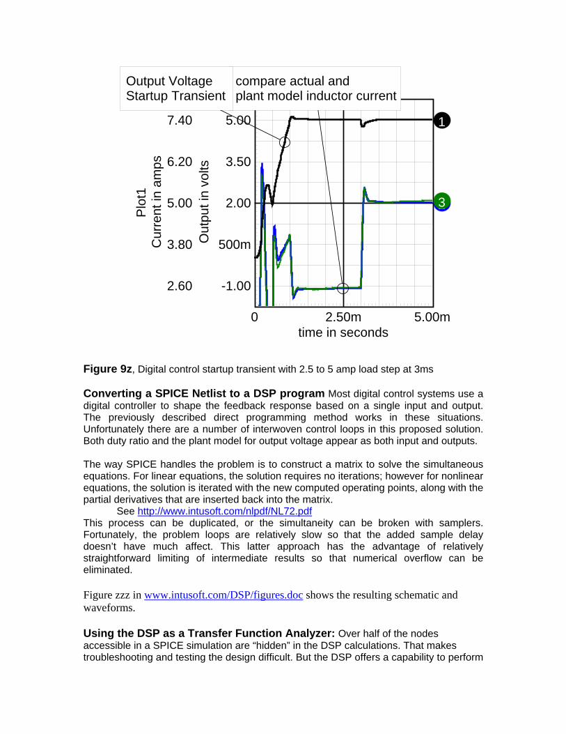
1 v(2) 2 i(vmxx) 3 v(iavgp)
0 2.50m 5.00mtime in seconds
-1.00
500m
2.00
3.50
5.00
Out
put i
n vo
lts
2.60
3.80
5.00
6.20
7.40
Cur
rent
in a
mps
Plo
t1
23
1
compare actual and plant model inductor current
Output Voltage Startup Transient
Figure 9z, Digital control startup transient with 2.5 to 5 amp load step at 3ms Converting a SPICE Netlist to a DSP program Most digital control systems use a digital controller to shape the feedback response based on a single input and output. The previously described direct programming method works in these situations. Unfortunately there are a number of interwoven control loops in this proposed solution. Both duty ratio and the plant model for output voltage appear as both input and outputs. The way SPICE handles the problem is to construct a matrix to solve the simultaneous equations. For linear equations, the solution requires no iterations; however for nonlinear equations, the solution is iterated with the new computed operating points, along with the partial derivatives that are inserted back into the matrix.
See http://www.intusoft.com/nlpdf/NL72.pdf This process can be duplicated, or the simultaneity can be broken with samplers. Fortunately, the problem loops are relatively slow so that the added sample delay doesn’t have much affect. This latter approach has the advantage of relatively straightforward limiting of intermediate results so that numerical overflow can be eliminated. Figure zzz in www.intusoft.com/DSP/figures.doc shows the resulting schematic and waveforms. Using the DSP as a Transfer Function Analyzer: Over half of the nodes accessible in a SPICE simulation are “hidden” in the DSP calculations. That makes troubleshooting and testing the design difficult. But the DSP offers a capability to perform
self-tests that have no analog counterparts. www.intusoft.com\DSP\TFA.doc illustrates how a transfer function analyzer can be built-in to the DSP firmware.
Test Results A Microchip SMPS Buck Development board with a DSPIC30F2020_SDIP300 DSP [5] was used to validate this design concept. First, the filter capacitor was changed from a conventional Aluminum electrolytic capacitor to an Aluminum-polymer capacitor to reduce ESR. The filter inductor was replaced with a higher current carrying part. Changes made after publishing this paper added a schottky diode across the upper switch and placed a ferrite bead in series with the upper and lower switches and added an input noise filter. Results are available in www.intusoft.com/DSP/DSP.zip Three different algorithms were coded. First a Proportional-Integral-Derivative, PID controller was implemented. That’s what the board started with, but the aluminum-polymer filter capacitor changed the problem. See “www.intusoft.com/DSP/Pid calculations.doc” for derivation of the new PID coefficients. Then the current sense built into the board was used to make a dual loop controller, current inner loop and PI outer loop control. That’s more inline with current SMPS technology. Next a new algorithm was coded using a plant model to extract current as a hidden variable without needing to measure current. As part of the hardware testing, the sine-cosine generator and transfer function analyzer were coded to make gain and phase measurements. A 5 Ohm pulsed load is built into the evaluation board. Several interesting properties of the board and micro controller include:
1. Independent PWM frequency and A/D Interrupt frequency 2. A/D Trigger control anywhere in the PWM cycle 3. Synchronous Buck topology makes active loading possible
The independent power conversion and data sample frequency allows optimization of power handling without being compromised by computational time requirements. There’s no real cliff to drop off of as the computational delay grows; the control performance degrades gradually. The analog controller performance is locked to the switching frequency and will consistently provide higher bandwidth than a DSP solution. A/D triggers can be used to sample the output voltage when switching noise is minimum. Synchronous power conversions results in negative current, which can’t be detected using the built-in high side sense circuit. That makes the current control using the plant model hidden variable even more attractive. Control system designers are averse to using derivative feedback because the noise is amplified, reducing the controllers dynamic range. In the worst case, the noise reduces gain so severely that low frequency large-scale oscillations occur. Designers usually use a derivative measuring device such as a tachometer or rate gyro in mechanical systems. The analog of that is the inductor current in an SMPS. Inner-loop current control also reduces input variation sensitivity. The Microchip Dualbuck evaluation board can be run in a synchronous switching mode. In that mode, inductor current is continuous and the converter can also operate in Boost mode to deliver power back into the load, using the same control loop dynamics. One of the converters can be used to load the other in order to simulate a load. An active load was made using a resistor connected between the 2 converters. Then one of the analog
inputs was used to control the voltage difference between the source and load. The sense resistor was selected to be 1 ohm, a bit larger than needed in order to reduce the interaction of the 2 control loops. Controlling the difference between the 2 “outputs” results in a constant current load while controlling the voltage of the second converter result in a resistive load simulation.
The test data in Figure pid shows how the 2 control loops respond to a 1 amp load step
1 vpid 2 vcur
4.00m 4.50m 5.00m 5.50m 6.00mtime in seconds
4.80
4.90
5.00
5.10
5.20
vpid
, vcu
r in
volts
Plo
t1 21
50mv/div250usec/div
Figure pid. Test results show the PID waveform ringing at the L-C resonant frequency. Both have the same initial peak disturbance, but the control loop using current feedback damps the ringing. Pk-Pk Duty ratio noise is 7% and 9% for the PID and current loop
respectively. The pid loop was run at Fs=100kHz and the Current loop Fs was 78kHz to accommodate the longer computational time. The plant model added about 3usec to the computational time. Noise is basically caused by errors in measuring the output voltage. These errors can be the result of various random noise sources, systematic interference from switching signals and A/D quantizing effects. Quantizing error dominates this application. Quantizing error causes the measured output to jump between levels (by a least significant bit, LSB) to achieve the average of the commanded signal. It looks like a mini SMPS within the main switching loop. The pk-pk error is amplified by the system gain from output to the duty ratio. Being aggressive with compensation (maximizing bandwidth) causes the gain to peak when the phase crosses zero. For the PID case, the gain is about 9, resulting in noise that’s 9*LSB=90m or 9% Duty ratio noise (measured 7%)). It’s about the same using current feedback. But combining the measured value of output voltage with the predicted value in the plant model reduces noise. For the example, the loop bandwidth was increased with respect to the switching frequency to achieve similar peak switching response. So the noise gain from the “Kalman” technique offsets the lower sampling frequency. The PID solution is an optimal controller for 2nd order systems when response to commanded change is desired. However, the SMPS problem is not concerned with response to reference voltage change. Instead, the power supply should be impervious to line and load changes. The current mode settling time and line sensitivity are much better than for a PID design. Since the system exceeds 2nd order, a slightly more complex control loop compensation would provide a bit higher bandwidth. Conclusion In summary, the plant model offers advantages in noise reduction and eliminates the current sense components used in a conventional SMPS. The complexity of the implementation requires a digital solution. Once the algorithm is designed, the only cost is the extra time for its solution. That cost drives toward zero over time as DSP price/performance ratios fall. With today’s technology, digital control performance is about the same as analog for switching frequencies below about 100kHz. For frequencies above 100kHz, the analog controller reduces output errors in proportion to switching period. In the future, the DSP needs to be faster and the A/D converter needs more bits in order to control quantizing noise as bandwidth is increased. The price/performance ratio is currently greater than required to use a DSP in low cost solutions such as wall adapters or compact fluorescent lamp controllers. Future DSP’s need to have reduced pin count as well as price. Coding DSP ‘s is very error prone, even passing through coding errors that appear to work. The design complexity level makes the decision to use these devices in new designs very difficult. The engineering effort is higher than for a comparable analog design. That leads to increased risk that must be mitigated by increased testing and analysis. Some of these shortcomings can be mitigated with improved software tools.
The very thing that makes DSP’s attractive, that is, the ease of adding features, results in a higher risk of introducing design flaws. Exposing the DSP design to increased scrutiny through testing and simulation is necessary. Footnote: Links to www.intusoft.com/DSP/… have more complete information. Files with .dwg and .grf extensions must be opened with Intusoft tools. These tools can be downloaded for free by going to www.intusoft.com/demos.htm. References: [1] BENJAMIN C. KUO, DIGITAL CONTROL SYSTEMS, 2nd EDITION, OXFORD UNIVERSITY PRESS, 1992 [2] CHRISTOPHE p. BASSO, SWITCH-MODE POWER SUPPLIES, MCGRAW HILL, 2008 [3] DR. DAVID MIDDLEBROOK, GENERAL FEEDBACK THEORM, GFT, INTUSOFT NEWSLETTER #70, MAY 2003 [4] ALAN V. OPPENHEIM,RONALD W. SHAFER , JOHN R. BUCK, DISCRETE-TIME SIGNAL PROCESSING, 2ND EDITION, PRENTICE HALL, 1998 [5] ANON, DSPICDEM™ SMPS BUCK DEVELOPMENT BOARD USERS GUIDE , , 2006