U.S. Government work not protected by U.S. copyright 1 A Novel Reconfigurable GaN Based Fully Solid-State Microwave Power Module for Communications/Radar Applications Rainee N. Simons, Life Fellow, IEEE NASA Glenn Research Center 21000 Brookpark Road Cleveland, OH 44135 216-433-3462 [email protected]Edwin G. Wintucky (Retired) NASA Glenn Research Center 21000 Brookpark Road Cleveland, OH 44135 Seth W. Waldstein NASA Glenn Research Center 21000 Brookpark Road Cleveland, OH 44135 216-433-5812 [email protected]Abstract—The paper presents as a proof-of-concept (POC) the design, integration, and performance of a novel reconfigurable S-/X-band, GaN based, fully solid-state microwave power module (SSMPM) to enable miniaturization of the overall RF system. The SSMPM includes diplexers, pre-amplifiers, a multistage medium power amplifier, SPDT switches, and CW/Pulsed high-power amplifiers. These components are synergistically integrated such that a single SSMPM is capable of being dynamically reconfigured to function as a CW S-/X- band amplifier for TT&C/science date downlink and as a pulsed X-band amplifier for remote sensing radar onboard a planetary exploration spacecraft. The POC SSMPM is capable of delivering Psat of 39 dBm (8 W CW) at S-band, Psat of 46 dBm (40 W CW) at X-band, and Psat of >50 dBm (>100 W Pulsed) at X-band. TABLE OF CONTENTS 1. INTRODUCTION ....................................................... 1 2. SOLID-STATE MICROWAVE POWER MODULE ..... 2 3. MEASURED RESULTS.............................................. 3 4. PROOF-OF-CONCEPT (POC) RECONFIGURABLE SSMPM AND TEST RESULTS ..................................... 5 5. CONCLUSION AND DISCUSSIONS............................ 6 REFERENCES............................................................... 6 BIOGRAPHY ................................................................ 7 1. INTRODUCTION Historically, the term microwave power module (MPM) is associated with a small fully integrated self-contained RF amplifier that combines both solid-state and microwave vacuum electronics technologies (Fig. 1) [1]. In this paper, we present the research and development of a novel fully solid-state microwave power module (SSMPM), which is distinctly different from the above MPMs [2]. The SSMPM advances the state-of-the-art in spacecraft transmitters. Our effort leverages from the recent advances in RF wide bandgap semiconductor (WBGS) crystal growth, wafer preparation, device/circuit fabrication technologies and reliability studies that have resulted from the investment that DARPA has made with the U.S. industry [3]. As a result of DARPA Figure 1. Schematic of a conventional microwave power module (MPM) based on both solid-state and microwave vacuum electronics technologies. investments, the past few years have witnessed significant progress in the development of GaN high electron mobility transistor (HEMT) on silicon carbide (SiC) substrate based monolithic microwave integrated circuits (MMICs) for RF power applications. The main advantages of GaN HEMT on SiC substrate is that it has power density as high as 12.2 watts/mm at X-band [4]. Thus, for a desired output power a GaN MMIC is smaller in size compared to a GaAs MMIC. In addition, SiC substrate has 8 to 10 times higher thermal conductivity than a GaAs substrate [5], which allows operating at higher junction temperature and also enhances thermal reliability by more efficiently conducting waste heat away from the junction. A typical payload on an Earth and planetary exploration spacecraft includes S-band system for telemetry, tracking, and command (TT&C) and a X-band or higher frequency telecommunication system for down linking data from science instruments. The role of the TT&C system is receiving commands and downlinking spacecraft house- keeping data. Typical science instruments are scatterometers, radiometers, and radar for synthetic aperture imagers. The role of the telecommunication system is to down-link science data acquired by these instruments. The current state of practice uses two separate S-band and X-band amplifiers in each of the above systems. However, due to the push for developing small satellites with enhanced system
Transcript
U.S. Government work not protected by U.S. copyright 1
A Novel Reconfigurable GaN Based Fully Solid-State Microwave Power Module for
Communications/Radar Applications Rainee N. Simons, Life Fellow, IEEE
NASA Glenn Research Center 21000 Brookpark Road Cleveland, OH 44135
Abstract—The paper presents as a proof-of-concept (POC) the design, integration, and performance of a novel reconfigurable S-/X-band, GaN based, fully solid-state microwave power module (SSMPM) to enable miniaturization of the overall RF system. The SSMPM includes diplexers, pre-amplifiers, a multistage medium power amplifier, SPDT switches, and CW/Pulsed high-power amplifiers. These components are synergistically integrated such that a single SSMPM is capable of being dynamically reconfigured to function as a CW S-/X-band amplifier for TT&C/science date downlink and as a pulsed X-band amplifier for remote sensing radar onboard a planetary exploration spacecraft. The POC SSMPM is capable of delivering Psat of 39 dBm (8 W CW) at S-band, Psat of 46 dBm (40 W CW) at X-band, and Psat of >50 dBm (>100 W Pulsed) at X-band.
TABLE OF CONTENTS
1. INTRODUCTION ....................................................... 1 2. SOLID-STATE MICROWAVE POWER MODULE ..... 2 3. MEASURED RESULTS .............................................. 3 4. PROOF-OF-CONCEPT (POC) RECONFIGURABLE SSMPM AND TEST RESULTS ..................................... 5 5. CONCLUSION AND DISCUSSIONS ............................ 6 REFERENCES............................................................... 6 BIOGRAPHY ................................................................ 7
1. INTRODUCTION
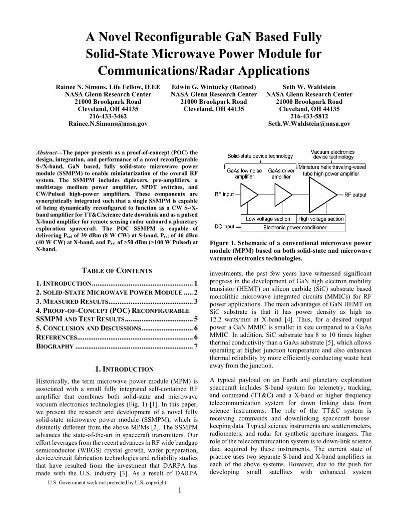
Historically, the term microwave power module (MPM) is associated with a small fully integrated self-contained RF amplifier that combines both solid-state and microwave vacuum electronics technologies (Fig. 1) [1]. In this paper, we present the research and development of a novel fully solid-state microwave power module (SSMPM), which is distinctly different from the above MPMs [2]. The SSMPM advances the state-of-the-art in spacecraft transmitters. Our effort leverages from the recent advances in RF wide bandgap semiconductor (WBGS) crystal growth, wafer preparation, device/circuit fabrication technologies and reliability studies that have resulted from the investment that DARPA has made with the U.S. industry [3]. As a result of DARPA
Figure 1. Schematic of a conventional microwave power module (MPM) based on both solid-state and microwave vacuum electronics technologies. investments, the past few years have witnessed significant progress in the development of GaN high electron mobility transistor (HEMT) on silicon carbide (SiC) substrate based monolithic microwave integrated circuits (MMICs) for RF power applications. The main advantages of GaN HEMT on SiC substrate is that it has power density as high as 12.2 watts/mm at X-band [4]. Thus, for a desired output power a GaN MMIC is smaller in size compared to a GaAs MMIC. In addition, SiC substrate has 8 to 10 times higher thermal conductivity than a GaAs substrate [5], which allows operating at higher junction temperature and also enhances thermal reliability by more efficiently conducting waste heat away from the junction.
A typical payload on an Earth and planetary exploration spacecraft includes S-band system for telemetry, tracking, and command (TT&C) and a X-band or higher frequency telecommunication system for down linking data from science instruments. The role of the TT&C system is receiving commands and downlinking spacecraft house-keeping data. Typical science instruments are scatterometers, radiometers, and radar for synthetic aperture imagers. The role of the telecommunication system is to down-link science data acquired by these instruments. The current state of practice uses two separate S-band and X-band amplifiers in each of the above systems. However, due to the push for developing small satellites with enhanced system
2
capabilities/performance at lower cost, it is advantageous to develop a single wideband, reconfigurable high-power, high-efficiency SSMPM that can operate at multiple frequency bands depending on the need at any given time. Additionally, a single dynamically reconfigurable amplifier enables miniaturization of the overall RF system. Innovations in compound semiconductor materials, devices, and circuits to increase the functionality and reconfigureability of RF systems are reported in [6], [7].
In this paper, we present as a proof-of-concept (POC) the design, integration, and performance of a novel reconfigurable S-/X-band GaN based fully solid-state MPM with a view to miniaturize the overall RF system. The module synergistically integrates diplexers, pre-amplifiers, multistage medium power amplifiers (MPAs), SPDT switches, and CW/Pulsed high power amplifiers (HPAs) with a voltage sequencer, a DC blanking controller, and a low voltage electronic power conditioner. The POC SSMPM operates at both S-band and X-band to serve multiple roles. The SSMPM can be reconfigured to deliver Psat of 39 dBm (8 W CW) at S-band, Psat of 46 dBm (40 W CW) at X-band, and Psat of >50 dBm (>100 W Pulsed) at X-band.
2. SOLID-STATE MICROWAVE POWER MODULE
Module Design and Mode of Operation
The SSMPM layout is schematically illustrated in Fig. 2. The typical frequencies at S-band and X-band for TT&C and telecommunications are 2.2 GHz and 8.4 GHz, respectively. At the input, a diplexer (D) selects either the S-band or the X- band signal to be processed. The two pre-amplifier stages
are GaAs based MMIC amplifiers that amplify the S-band and the X-band output signals from the diplexer respectively, to a level appropriate to drive the common multistage MPA. The switch is a non-reflective silicon single-pole, double throw (SPDT) device. The multistage MPA is high efficiency GaN HEMT PAs with output power (Pout) sufficient to drive the HPA stage. The HPAs are also high-efficiency GaN HEMT PAs that provide CW or pulsed power. As opposed to conventional amplifiers with external input/output matching networks, which take up relatively large area of dielectric substrate for microwave circuitry, the MPA and the HPA are designed with internally matched transistors that enables miniaturizing the overall SSMPM [8].
An electronic power conditioner (EPC) provides the gate and drain voltages and currents for the above amplifier stages. The EPC is a DC-to-DC power convertor that transforms the spacecraft bus voltage typically in the range of +21 V and +35 V into regulated voltages required by the amplifier stages. In addition, a DC power management circuit is included to manage the correct power-up and power-down sequence. That is to ensure that the negative gate voltages are applied before the positive drain voltages are applied to turn the amplifiers ON. Furthermore, a DC blanking control is also provided to quickly turn the amplifiers OFF if a fault condition arises. Moreover, a RF output monitor such as a temperature sensor or a detector/reference diode pair is located near or on the high-power GaN die, in the output stage, to monitor for an over temperature condition. The detector/reference diode pair also monitors the RF output power level. The packaged SSMPM unit will be conduction cooled.
Figure 2. Schematic of a fully solid-state microwave power module (SSMPM) based on high power GaN MMIC Power Amplifiers.
3
3. MEASURED RESULTS In this section, the measured performance of the diplexer, pre-amplifiers, SPDT switch, MPA, and HPA under CW and pulsed operating conditions are presented. The MPA and the HPA were maintained at 25 °C base plate temperature during characterization by attaching them to Peltier-thermoelectric cold plate coolers.
Diplexer
The diplexer is Marki Microwave Model DPX-4 and is housed in a miniature connectorized package. The measured insertion loss from the input to the output low-pass (LP) (S-band) and the high-pass (HP) (X-band) coaxial ports are on the order of 0.8 dB and 1.0 dB at the S-band and X-band respectively. The passband return loss and the common port return loss are better than 10 dB. The isolation is better than 25 dB. These results are presented in Fig. 3.
Pre-Amplifiers
The two Avantek pre-amplifiers, model AWT-6035 operating from 2-6 GHz and model AMT-12436 operating from 7-12.4 GHz, each provides a gain of about 50 dB with output power and gain presented as a function of frequency in Fig. 4.
SPDT Switch
The switch is an Analog Devices Model HMC1118 and is a nonreflective single-pole, double-throw (SPDT) type that operates over a wideband (9 kHz-13 GHz), which allows reconfiguring the SSMPM to function at either S- or X-band. In addition, the switch is internally matched to 50 ohms at the RF input port and the RF output ports and hence requires no external matching components. The HMC1118 is housed inside a 3 x 3 mm surface mount package. The measured insertion loss of the switch when the two inputs are sequentially turned ON is on the order of 0.6 and 1.4 dB at S-band and X-band, respectively. The measured isolation between the two output ports of the switch is greater than 50 dB and 40 dB at S-band and X-band, respectively.
Wideband GaN Multistage Medium Power Amplifier (MPA)
The first stage of the wideband MPA is built with a Qorvo Model TGA2214-CP MMIC, which has 0.15 µm gate transistors fabricated on GaN-on-SiC substrate and operates from 2-18 GHz. The input and output RF ports of the MMIC have integrated DC blocking capacitors and are fully matched to 50 ohms. Furthermore, the MMIC package has pure copper base offering superior thermal management. The second stage of the MPA is built with Analog Devices Model HMC1087F10 GaN MMIC that operates from 2-20 GHz. The MMIC input and output ports are internally matched to 50 ohms. Moreover, the MMIC package body material is copper tungsten (15Cu85W). The measured Pout and gain of each stage at S-band (2.15 GHz) and X-band (8.475 GHz) as a function of input power are presented in Fig. 5(a). The corresponding measured PAEs are presented in Fig. 5(b). The
Figure 3. Measured diplexer insertion loss at the low-pass (S-band) and high-pass (X-band) coaxial ports.
Figure 4. Measured output power and gain as a function of the input drive at S-band (2.15 GHz) for Avantek AWT-6035 with VD = 12 V, IDQ = 310 mA and at X-Band (8.475 GHz) for Avantek AMT-12436 with VD = 12 V, IDQ = 350 mA.
Psat of the first stage is 37 dBm, the corresponding gain is 20 dB, and the PAE is 25%. The Psat of the second stage is 39.5 dBm, the corresponding gain is 8.8 dB, and the PAE is 27%.
GaN CW High-Power Amplifier (HPA)
The CW HPA stage is configured either as a single Sumitomo Model SGK77850-30A GaN high electron mobility transistor (HEMT) based MMIC amplifier or as two SGK77850-30A amplifiers in a balanced configuration. The MMIC amplifier is internally matched to 50 ohms. The balanced amplifier, with topology shown in Fig. 6 employs hybrid couplers (Narda Model 4356B, 2-18 GHz) at the input and output to divide and combine the power, respectively. The measured results are presented in Fig. 7. The Psat of the single HPA is 43.5 dBm, the corresponding gain is 7.9 dB, and the PAE is 36.7%. The Psat of the balanced HPA is 46.7 dBm, the corresponding gain is 6.8 dB, and the PAE is 34%.
4
(a) (b)
Figure 5. (a) Measured output power and gain as a function of the input drive, and (b) Measured PAE as a function of the input power, for the MPA 1st stage with TGA2214-CP: VD = 22 V, VG = -2.3 V, IDQ = 600 mA and 2nd stage with HMC1087F10: VD = 28 V, VG = -2.3 V, IDQ = 850 mA.
Figure 6. Balanced amplifier configuration consisting of two Sumitomo SGK77850-30A HPA and Narda Model 4356B hybrid couplers.
(a) (b)
Figure 7. (a) Measured output power as a function of the input drive, and (b) Measured PAE as a function of the input drive at X-band (8.475 GHz), for a single Sumitomo SGK77850-30A with VD = 24 V, VG = -2.2 V, IDQ = 1750 mA and balanced amplifier with VD = 24 V, VG = -2.2 V, IDQ = 3500 mA.
5
(a) (b)
Figure 8. (a) Measured peak output power and gain as a function of the input drive, and (b) Measured peak PAE as a function of the input drive at X-band (8.475 GHz), for Cree CGHV96100F2 under pulsed conditions, duty cycle = 10%, pulse width = 100 µsec, VD = 40 V, VG = -2.2 V, IDQ = 1000 mA.
Figure 9. A POC bread board version of the fully assembled reconfigurable SSMPM as a pre-cursor to a compact SSMPM. (1) Marki Microwaves DPX-4, (2) Avantek AMT-12436, (3) Avantek AWT-6035, (4) Analog Devices HMC1118 SPDT, (5) Qorvo TGA2214-CP, (6) Analog Devices HMC1087F10, (7) Ducommun 2SM001, (8) Narda 4356B Hybrid Coupler, (9) Sumitomo SGK77850-30A, (10) Thermocouple, (11) Cree CGHV96100F2.
GaN Pulsed High-Power Amplifier (HPA)
The pulsed HPA is realized with a Cree Model CGHV96100F2 MMIC, which has GaN HEMT on SiC substrate that are internally matched to 50 ohms. The MMIC is housed inside a metal/ceramic flanged package for optimal thermal performance. The measured characteristics under pulsed operating conditions is presented in Fig. 8. The Psat of the pulsed HPA is 50.86 dBm, the corresponding gain is 9.86 dB, and the PAE is 34.5%.
4. PROOF-OF-CONCEPT (POC) RECONFIGURABLE SSMPM AND
TEST RESULTS A POC bread board version of the fully assembled reconfigurable SSMPM with the diplexer, pre-amplifers, SPDT switch, MPA, and HPA presented earlier is shown in Fig. 9. The measured output power of the end-to-end S-band, X-band (CW), and X-band (Pulsed) chains are presented in Fig. 10. The signal pathways are shown in the inset in
6
Figure 10. Measured output power as a function of the input drive for the S-band (CW), X-band (CW), and X-band (Pulsed) signal pathways that are shown in the inset.
Fig. 10. The results indicate that the S-band CW chain of the SSMPM delivers Psat of 39 dBm (8 W) for TT&C, the X-band CW chain delivers Psat of 46 dBm (40 W) for telecommunications, and the X-band pulsed chain without the pre-amplifiers delivers Psat of >50 dBm (>100 W) for radar applications.
5. CONCLUSION AND DISCUSSIONS The paper presents as a proof-of-concept the design, integration, and performance of a novel reconfigurable, S-/X-band GaN MMIC based, fully solid-state microwave power module (SSMPM) with a view to miniaturize the overall RF system. The characterization of the individual components as well as the end-to-end performance of each of the S-band and X-band chains of the SSMPM are presented. These results indicate that the S-band CW chain can deliver Psat of 39 dBm (8 W) for TT&C, the X-band CW chain can deliver Psat of 46 dBm (40 W) for telecommunications, and the X-band pulsed chain without the pre-amplifiers can deliver Psat of >50 dBm (>100 W) for radar applications.
Our link budget calculations indicate that the SSMPM with Psat = 40 W when coupled to a 10 cm X-band transmit antenna on a low Earth orbiting (900 km) satellite can close a 1 Gbps (QPSK) data downlink to a 1 m receive antenna on ground with 3 dB margin.
Leveraging upon compound semiconductor devices and novel materials [7] will enable the monolithic heterogeneous integration of GaN plus CMOS for realization of a compact SSMPM. The above results indicate that a single SSMPM is capable of being dynamically reconfigured to serve multiple roles such as an amplifier for TT&C, telecommunications, and radar onboard future Earth and planetary exploration spacecrafts.
As a final note, GaN HEMT based X-band power amplifiers when tested under conditions in low Earth orbit during a five-year mission, have shown to be tolerant to a total ionizing dose of 20k rads when placed inside a 2 mm thick aluminum shielding enclosure [9].
REFERENCES [1] J.X. Qiu, B. Levush, J. Pasour, A. Katz, C.M. Armstrong,
D.R. Whaley, J. Tucek, K. Kreischer, and D. Gallagher, “Vacuum Tube Amplifiers,” IEEE Microwave Magazine, Vol. 10, No. 7, pp. 38-51, Dec 2009.
[2] R.N. Simons and E.G. Wintucky, U.S. Patent No. 9,041,469 B1, “High-Efficiency Power Module,” May 26, 2015.
[3] M.J. Rosker, J.D. Albrecht, E. Cohen, J. Hodiak, T.-H. Chang, “DARPA’s GaN Technology Thrust,” 2010 IEEE MTT-S International Microwave Symposium Digest, pp. 1214-1217, Anaheim, CA, May 23-28, 2010.
[4] R. Chu, L. Shen, N. Fichtenbaum, D. Brown, Z. Chen, S. Keller, S.P. DenBaars, and U.K. Mishra, “V-Gate GaN HEMTs for X-band Power Applications,” IEEE Electron Device Letters, vol. 29, no. 9, pp. 974-976, Sept 2008.
[5] R.T. Kemerley, H.B. Wallace, and M.N. Yoder, “Impact of Wide Bandgap Microwave Devices on DoD Systems,” Proc. IEEE, Vol. 90, No. 6, pp. 1059-1064, June 2002.
[6] S. Hary, T. Barton, and J. Ebel, “Reconfigurable RF Components for Multifunction RF Systems,” 2016 IEEE Compound Semiconductor Integrated Circuit Symposium (CSICS) Technical Digest, pp. 20-23, Austin, TX, Oct 23-26, 2016.
7
[7] D.S. Green, C.L. Dohrman, A.S. Kane, and T.-H. Chang, “Materials and Integration Strategies for Modern RF Integrated Circuits,” 2014 IEEE Compound Semiconductor Integrated Circuit Symposium (CSICS), pp. 1-4, La Jolla, CA, Oct 19-22, 2014.
[8] R.S. Pengelly, J. Arnold, J. Cockrill, and M.G. Stubbs, “Prematched and Monolithic Amplifiers Covering 8-18 GHz,” 9th European Microwave Conference Proceedings, pp. 293-297, Brighton, UK, Sept 17-20, 1979.
[9] H. Watanabe, O. Ceylan, H. Saito, A. Tomiki, H. Nunomura, O. Shigeta, N. Iwakire, T. Shinke, and T. Fukami, “High-Efficiency X Band GaN Power Amplifier for Small Satellite Downlink System,” 2013 IEEE MTT-S International Microwave Symposium (IMS) Digest, Seattle, WA, June 2-7, 2013.
BIOGRAPHY Rainee N. Simons received the B.S. degree in electronics and communica-tions engineering (E&CE) from the Mysore University, India, in 1972, and the M.Tech. degree in E&CE from the Indian Institute of Technology (IIT), Kharagpur, India, in 1974 and the Ph.D. degree in
electrical engineering from the IIT, New Delhi, India in 1983. He was a Senior Scientific Officer with the IIT, New Delhi, from 1979-1985. Dr. Simons was a National Research Council Post Doctoral Research Associate at NASA Glenn from 1985-1987. Since 1987 he is with the NASA Glenn Communications Technology Division. At NASA Glenn he served as the Chief of the Electron Device Technology Branch and as a Senior Microwave and Antenna Systems Engineer. Since November 2017, he is serving as the Program Officer for the Maturation of Instruments for Solar System Exploration (MatISSE) in the Planetary Science Division, NASA Headquarters, Washington, DC. Dr. Simons has authored two books and five book chapters. Furthermore, he has authored or co-authored over 180 publications in refereed journals and international symposium proceedings and 75 NASA Technical Memorandums. Moreover, he has been awarded eleven U.S. patents. Dr. Simons is a recipient of the Distinguished Alumni Award from his alma mater. In addition, he has received over 30 NASA Certificates of Recognitions/Tech Brief Awards, five NASA Space Act Awards, four NASA Group Achievement Honor Awards, NASA Public Service Medal, NASA Outstanding Leadership Medal, and the NASA Exceptional Technology Achievement Medal. Furthermore, he has received two R&D100 Awards for the development of K-band and Ka-band space TWTAs, respectively. Moreover, he received the status of runner-up in the wireless category from the Wall Street Journal’s 2009 Technology Innovation Award program and the 2010
NorTech Innovation Award form Crain’s Cleveland Business for the development a BioMEMS sensor.
Dr. Simons has organized workshops, chaired sessions, and served on the Technical Program Committees of several IEEE International Symposiums. He has served as an Associate Editor of the IEEE Transactions on Antennas and Propagation. Dr. Simons is a Life Fellow of the IEEE.
Edwin G. Wintucky received a B.Sc. degree from the Ohio State University and an M.S. degree from Kent State University, both in Physics. He has been with NASA since 1964 and has worked on a variety of programs that includes electric propulsion and space communications. Until recently, his
work in space communications was focused on cathode technology research and development, where he served as NASA’s representative in that area. More recently he has been involved with the development of communications and remote sensing applications for high power Ka-band traveling wave tubes that includes high power combining and dual frequency Doppler radar. Recently, Mr. Wintucky retired with over 50 years of service to NASA and the United States Federal Government.
Seth W. Waldstein received the B.F.A. in Music Performance from the New School University in New York City in 2009 and the B.S. in Electrical Engineering from the University of Cincinnati in 2017. He is currently a PhD candidate in Electrical
Engineering Department at the University of Cincinnati in Cincinnati, OH along with being a Pathways Intern in the Advanced High Frequency Branch at the NASA Glenn Research Center in Cleveland, Ohio.


![Ours w/o GAN Ours w/ GAN arXiv:1804.02900v2 [cs.CV] 10 …A Fully Progressive Approach to Single-Image Super-Resolution Yifan Wang 1,2 Federico Perazzi 2 Brian McWilliams 2 Alexander](https://static.documents.pub/doc/80x56/5ecaa6edf28e6d221c178609/ours-wo-gan-ours-w-gan-arxiv180402900v2-cscv-10-a-fully-progressive-approach.jpg)


