A NOVEL ROM COMPRESSION TECHNIQUE AND A HIGH SPEED SIGMA- DELTA MODULATOR DESIGN FOR DIRECT DIGITAL SYNTHESIZER Except where reference is made to the work of others, the work described in this thesis is my own or was done in collaboration with my advisory committee. This thesis does not include proprietary or classified information. Malinky Ghosh Certificate of Approval: Richard C. Jaeger Distinguished University Professor Electrical and Computer Engineering Guofu Niu Professor Electrical and Computer Engineering Fa Foster Dai, Chair Associate Professor Electrical and Computer Engineering Stephen L. McFarland Acting Dean Graduate School
Transcript
A NOVEL ROM COMPRESSION TECHNIQUE AND A HIGH SPEED SIGMA-
DELTA MODULATOR DESIGN FOR DIRECT DIGITAL SYNTHESIZER
Except where reference is made to the work of others, the work described in this thesis is my own or was done in collaboration with my advisory committee. This thesis does not
include proprietary or classified information.
Malinky Ghosh
Certificate of Approval: Richard C. Jaeger Distinguished University Professor Electrical and Computer Engineering
Guofu Niu Professor Electrical and Computer Engineering
Fa Foster Dai, Chair Associate Professor Electrical and Computer Engineering Stephen L. McFarland Acting Dean Graduate School
A NOVEL ROM COMPRESSION TECHNIQUE AND A HIGH SPEED SIGMA-
DELTA MODULATOR DESIGN FOR DIRECT DIGITAL SYNTHESIZER
Malinky Ghosh
A Thesis
Submitted to
the Graduate Faculty of
Auburn University
in Partial Fulfillment of the
Requirements for the
Degree of
Master of Science
Auburn, Alabama May 11, 2006
iii
A NOVEL ROM COMPRESSION TECHNIQUE AND A HIGH SPEED SIGMA-
DELTA MODULATOR DESIGN FOR DIRECT DIGITAL SYNTHESIZER
Malinky Ghosh
Permission is granted to Auburn University to make copies of this thesis at its discretion, upon request of individuals or institutions and at their expense. The author reserves all
publication rights.
________________________________ Signature of Author
________________________________ Date of Graduation
iv
THESIS ABSTRACT
A NOVEL ROM COMPRESSION TECHNIQUE AND A HIGH SPEED SIGMA-
DELTA MODULATOR DESIGN FOR DIRECT DIGITAL SYNTHESIZER
Malinky Ghosh
Master of Science, May 11, 2006 (B.E., Nagpur University, 2002)
92 Typed Pages
Directed by Foster Dai
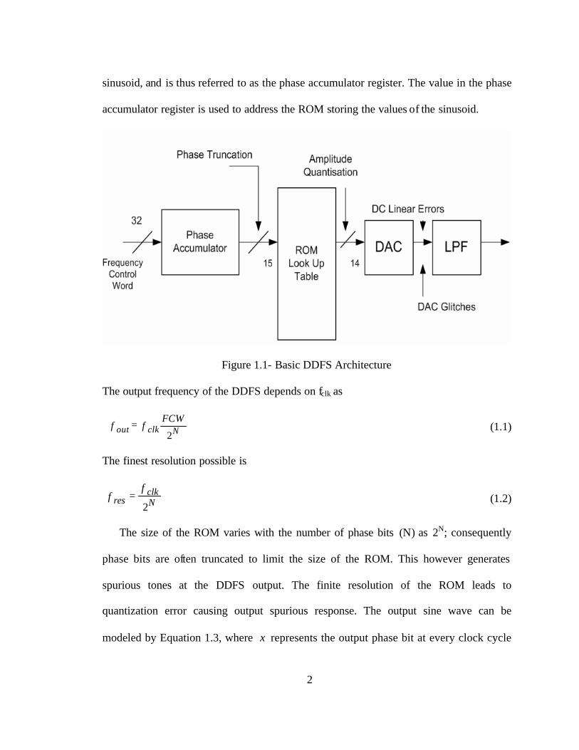
Traditional designs of high bandwidth frequency synthesizers employ phase locked
loops (PLLs). A direct digital frequency synthesizer (DDFS) provides multiple
advantages over the frequency synthesizers that use PLLs. A DDFS has fast settling time,
high frequency resolution, continuous phase switching response and low phase noise.
Traditionally, DDFSs were mainly used in producing narrow bands of closely spaced
frequencies. However, recent advancements in integrated circuit (IC) technologies have
provided a vast scope for progress in this area.
The use of DDFS is still in developmental stages. However, its major bottleneck is
the presence of a phase to sine converter ROM look-up-table which restricts speed,
occupies large area and has high power consumption.
v
This thesis presents a novel DDFS ROM compression technique that provides high
compression ratio without performance degradation. To validate the proposed DDFS
ROM compression algorithm, architectures are implemented in a Xilinx Spartan II FPGA
and their spurious performances are compared. A theoretical analysis in the first part of
the thesis gives an overview of the functionality of DDFSs and sigma-delta modulators
with respect to noise and spurs. Other popularly used ROM compression techniques are
discussed and compared to the proposed technique. The later part of the thesis deals with
the design and implementation of a sigma-delta modulator used to reduce the phase noise
at the output of a ROM less DDFS architecture.
vi
ACKNOWLEDGMENTS
It is a pleasure to thank all the people who made this thesis possible. I am deeply
indebted to my advisor Prof. Dr. Foster Dai whose help and encouragement motivated me
during the course of this research. I am grateful to Dr. Richard Jaeger and Dr. Guofu Niu
for their suggestions. Lastly and most importantly, I thank my parents and Debjit for their
support during the course of this work.
vii
Style Manual or Journal used: GUIDE TO PREPARATION AND SUBMISSION OF THESIS AND DISSERTATION 2005
Computer Software used: MS - Word
viii
TABLE OF CONTENTS
LIST OF FIGURES ix LIST OF TABLES xii
1 INTRODUCTION 1
1.1 Basic Direct Digital Frequency Synthesizer 1 1.2 Overview of Work 4
2 A NOVEL ROM COMPRESSION TECHNIQUE FOR DDFS 6
2.1 Background of Compression Techniques 6 2.1.1 Sine Quadrature Symmetry Algorithm 11 2.1.2 Sine Phase Difference Algorithm 12
2.2 Proposed Architecture 13 2.2.1 Architecture with Linear Addressing 17 2.2.2 Architecture with Non Linear Addressing 21
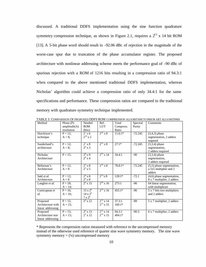
212 x 8 78.8:1* -72.245 (5,5) phase segmentation, a 5x5 multiplier and 2 adders
Said et al. Architecture
P = 12; A = 8
24 x 8 24 x 8
212 x 8 128:1* -72.1 (4,6) phase segmentation, 8 x 7 multiplier, 2 adders
Langlois et al. P = 18; A = 14;
26 x 15 214 x 16 273:1 -96 64 linear segmentation, with multiplexer
Curticapean et al.
P = 16; A = 16;
15 x 26
14 x 26
7 x 26
216 x 16 455:1* -96 5 x 7 bits two multipliers and 2 adders
Proposed Architecture with linear addressing
P = 15; A = 15;
28 x 12 213 x 14 215 x 15
37.3:1 160:1*
-89 5 x 7 multiplier, 2 adders
Proposed Architecture non linear addressing
P = 15; A = 15;
26 x 13 25 x 12
213 x 14 215 x 15
94.3:1 404:1*
-90.3 6 x 7 multiplier, 2 adders
* Represents the compression ration measured with reference to the uncompressed memory instead of the otherwise used reference of quarter sine wave symmetry memory. The sine wave symmetry memory = (¼) uncompressed memory
11
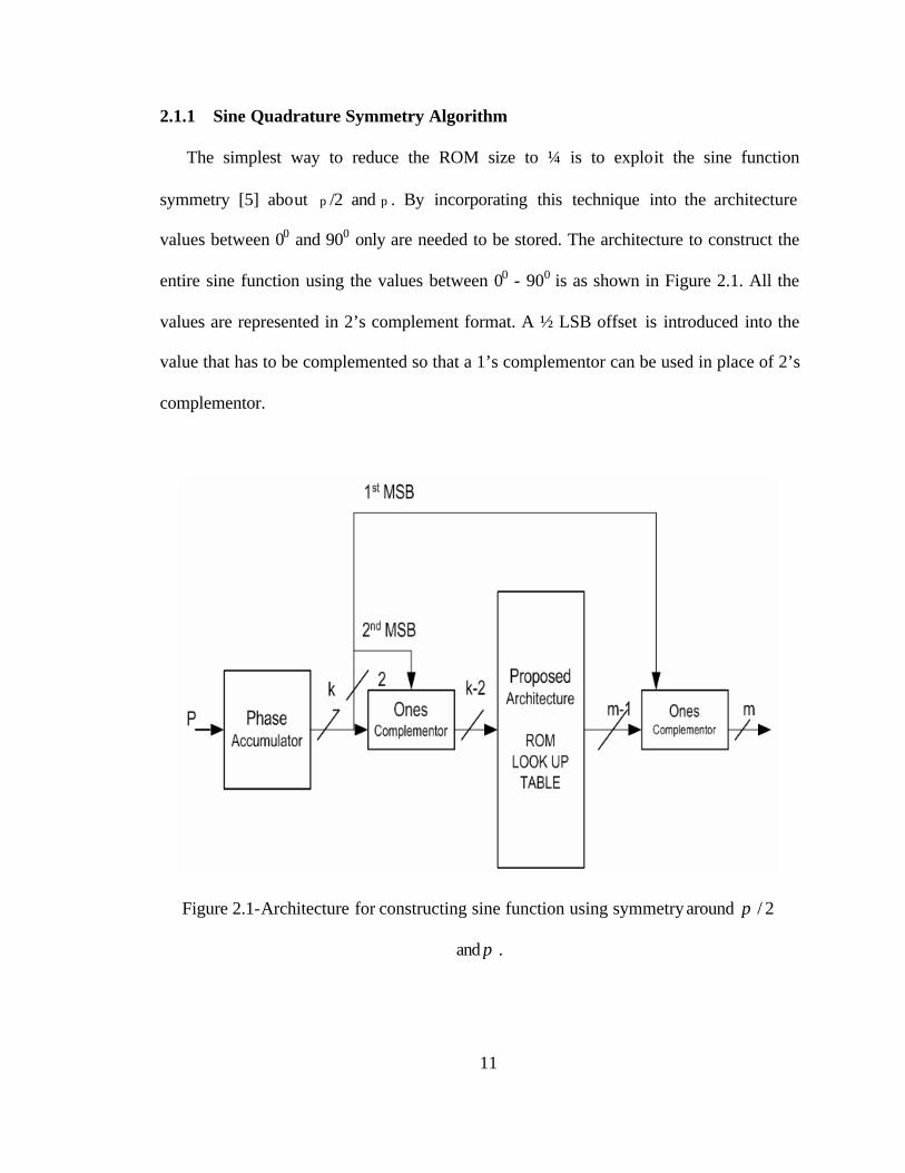
2.1.1 Sine Quadrature Symmetry Algorithm
The simplest way to reduce the ROM size to ¼ is to exploit the sine function
symmetry [5] about p /2 and p . By incorporating this technique into the architecture
values between 00 and 900 only are needed to be stored. The architecture to construct the
entire sine function using the values between 00 - 900 is as shown in Figure 2.1. All the
values are represented in 2’s complement format. A ½ LSB offset is introduced into the
value that has to be complemented so that a 1’s complementor can be used in place of 2’s
complementor.
Figure 2.1-Architecture for constructing sine function using symmetry around 2/π
and π .
12
2.1.2 Sine Phase Difference Algorithm
Sine phase difference algorithm [5] is one of the popular techniques of compression
used in almost all the compression algorithms proposed. In this algorithm, the
compression of ROM required for quarter wave sine function is obtained from the
function
xx
xf −
=2
sin)(π
(2.2)
Instead of sin ( π x/2); function f(x) is stored instead of sin (π x/2). Two bits of amplitude
are saved in the ROM by incorporating this algorithm without degradation in the spurious
response. But this algorithm requires an additional adder at the output of the ROM to
calculate the function
xxf +)( (2.3)
In the proposed architecture this algorithm is used to reduce the ROM size from 1408
bits to 1216 bits.
2.2 Proposed Architecture
In DDFS architectures that use ROM compression techniques, certain samples of the
sinusoid are stored in the ROM, and the entire sinusoid is created by calculating the
interpolation values using these stored values. In our architecture, the two most popular
13
techniques of storage reduction (i) sine function quadrature symmetry and (ii) sine phase
difference algorithm have been used. The sine phase difference algorithm technique
stores the value of sin(x) – x instead of the value of the corresponding sine sample. An
adder is used later to add the phase word to the value stored in the ROM. This technique
helps to reduce the width of the word that is stored in the ROM by 2 bits. Incorporating
this technique in our architecture requires 2 additional adders.
At any clock cycle the value in the phase register indicates the phase of the sine
function. As not all the samples of the sinusoid are stored, only the first m bits of the N-
bit phase word are used for addressing the ROM. The remaining d bits (d = N-m) are
used calculate the value and position of the interpolation point. The first order linear
interpolation formula is presented where sin (A) and sin(C) are the successive stored
sinusoid samples.
xACAB ∆×−+= ))sin()(sin()sin()sin( (2.4)
sin(B) is the sample to be interpolated and is calculated using the above equation. sin(A)
is the sine value addressed by the phase bits in the present clock cycle and sin (C) is the
next ROM sample. The value of ?x is obtained using the d least significant bits of the
phase word. There can be a maximum of 2d interpolation points between the successive
stored values of the ROM. Maximum number of samples are interpolated when the input
frequency control word (FCW) is 1. The value in the phase registers at any instant reads
R as given in the following equation.
14
)1( −×= iFCWR (2.5)
Here i denotes the number of clock cycles. R[(N-1):0] represents an N-bit word with
bit (N-1) as its MSB and bit 0 as its LSB. The notation is used in Verilog hardware
description language. The phase angle of every sinusoid sample to be interpolated is
calculated by Equation (2.6) and the interpolated value is given by Equation (2.7).
[ ]
−
== N
tt
NRBX2
0:12π
(2.6)
( )]0:1[)2(
)sin(sin)sin()sin( −×
−+= dR
ACAB d (2.7)
In other words, the d least significant bits of the phase register output R indicate the
relative position of the interpolated sample from the preceding stored sample.
Consequently it also represents the number of clock cycles required for the value in the
phase register to change from A to B. The output of the ROM has a word length and
hence amplitude resolution of k-bits. In the proposed architecture, the sine function is
assumed to be piecewise linear. In order to avoid the division in Equation (2.7) which
involves hardware, the formula has been modified to equation (2.8)
The subscripts 2 and 1 indicate that the values under discussion are from ROM2 and
ROM1 respectively. d2 is one bit greater than d1(d1 = d = N-m). If the widths of both
ROM1 and ROM2 are taken as k bits, as in the linear addressing scheme, shifting the
)sin( 2A value by d2 as given in Equation 2.9 will make the output word length as k + d +
1 bits. In order to have uniform output, the width of ROM2 is made k-1 instead of k. The
memory requirements for this architecture are 2m-1 x k + 2m-2 x (k-1) bits.
17
2.2.1. Architecture with Linear Addressing
Without losing generality, a phase precision of 15 bits and a ROM of 28 bits with
amplitude resolution of 14 bits are used to simulate the proposed architecture as shown in
Figure 3. The width of ROM is reduced from 14 bits to 12 bits due to incorporation of the
sine-phase difference algorithm. The block marked as the sine phase difference algorithm
a DDFS the value of phase angle (A) back to the output of the ROM (sin A - A) such that
at the output of this block is sin A value with 14- bit resolution. Thus the actual ROM size
is 28 x 12 bits.
As a ROM of length 28 has been used, 256 sinusoid samples for phase angles of 00 - 900
are stored in the ROM. For a phase accumulator of length 15 bit, phase accumulator
output word is represented as R[14:0] where bit 14 is MSB and bit 0 is LSB. The first 2
bits out of the 15 bits of the phase accumulator register indicate the quadrant of the sine
wave.
The remaining 13 bits are therefore used to address the sine wave between 00-900. As the
ROM has 256 values, the 8 MSB bits of output phase word R[12:5], i.e. 12th bit to 5th
bit of the phase word R, are used for addressing the ROM. From Equation 2.8, we require
the value stored at the present location (sin A) as well as the value stored in the
successive location (sin C) for the interpolation technique. Figure 3 shows the control
circuitry which accomplishes this goal. Value of sin A, pointed by R[12:5], is obtained in
the present cycle. The control circuit a DDFS a 1 to R[12:5] to point to the successive
ROM location such that the value of sin C is obtained in the next cycle. EN is double the
clock frequency, such that as EN = 1, output of the control circuit points to location of sin
A and EN = 0, it points to location of sin C. As the truncated bits are 2d = 2 (13-8) = 32, the
18
phase register points to a particular ROM value for 32 clock cycles for FCW = 1.
For FCW = 1, d is given by LSB 5 bits of R, thus the sample values obtained from the
ROM are shifted left by 5 positions, which is the same as multiplying it by 32, and later
truncated according to the size of the DAC. As in Figure 3 this is implemented using a 5-
bit shift register. The shifted ROM value is added to the output of the multiplier that
realizes the first part of Equation 2.9. From Figure 3, the inputs to the multiplier are: sin
(C) – sin (A), obtained from the subtractor and the LSB bits of output phase word denoted
by R[d-1:0].
The sine phase difference algorithm is introduced in the architecture to reduce the width
of the ROM by 2 bits. The values stored in the ROM thus change to (sin (x) – x) where x
is the phase angle of the sinusoid. The inputs to the sine phase difference adder are the
phase given by W (R[m-1:0]) and the output of the ROM as shown in Figure 2.3.
Therefore the bit length of the output of the block is 14 bits.
The overall sine value is represented with a precision of 14 + 5 = 19 bits. This value is
truncated to 14 bits before being sent to the DAC. The -90 dBc SFDR is obtained for
output amplitude resolution of 15-bits. Truncation to 14 bits gives the best spurious
response when compared to truncation to either 15 or 13 bits, because in this case the
output becomes 15-bits with the MSB sign bit. In order to achieve about the same
quantization noise floor due to phase truncation and finite amplitude bits, the number of
phase bits is required to be larger than or equal to the number of amplitude bits. So
truncation to 14 bits is considered to be optimal. This technique of shifting the ROM
value and adding the multiplier value to it to obtain the sine output increases the precision
of the output and reduces the complexity of calculations required to obtain the sine values
19
that have to be interpolated.
Figure 2.2 - Sine wave divided in to 22 parts when ROM is 22x 4 bit.
Figure 2.3 - Phase to Sine conversion architecture with accumulator and counter.
20
Figure 2.4 - Phase to Sine conversion architecture with linear addressing using Multiplier.
Figure 2.5 - Phase to Sine conversion architecture with non-linear addressing
21
2.2.2. Architecture with Non-linear Addressing
For the architecture with two ROMs, the sinusoid is partitioned in two parts; 00-450
and 450-900 as shown in Figure 4. The sine values for phase between 00-450 are stored in
ROM1, and 450-900 in ROM2. The phase accumulator is taken to be 15 bits long. The
width of the ROMs are taken to be 14 bits and 13 bits, but due to the architecture having
sine phase difference algorithm incorporated in it, the ROM sizes are given by ROM1
equal to 26 x 12 bits and ROM2 equal to 25 x 11 bits. The explanation of ROM2 width
being lesser than ROM1 width is given in section II A. The mentioned ROM sizes require
the number of samples interpolated between successive stored values to be 64 between
00-450 and 128 in between 450-900 if FCW = 1. The address lines required to address
ROM1 are 7 given by R[12:6] and those required for ROM2 are denoted by 6-bits,
R[12:7]. The sine phase difference algorithm is incorporated using a single adder. The
inputs to the adder is obtained from the phase bits addressing ROM1 or ROM2 at any
clock cycle and ROM output that is any one of sin(A1)-A1, sin(A2)-A2, sin(C1)-C1 or
sin(C2)-C2 at any clock cycle. The phase bits addressing ROM1 or ROM2 are selected
using a multiplexer enabled by the (N-2)th -bit denoted as R[12].
The output of the subtractor is given by sin(C1,2) - sin(A1,2). In accordance with
Equation 2.9 and 2.10, the values of ROM1 are shifted left by d1 = 6 bits and the values
of ROM2 are shifted by d2 = 7 bits before being added to the multiplier output to obtain
the sinusoid sample. The multiplier input is given by R[d1-1:0] = R[5:0] or R[d2-1:0] =
R[6:0] for ROM1 and ROM2 respectively and the corresponding values of sin (C1,2)-sin
(A1,2).
The whole sine value is represented with a precision of 15 + 6 = 21 bits. This value is
22
truncated to 14 bits before sending to the DAC.
The proposed technique requires additional hardware of a 7 x 8 bit multiplier, shift
registers and subtractor. Thus the increase in the hardware overhead is the trade off for
the great reduction in the memory requirement.
The sinusoid can further be partitioned to 00-300, 300-600, 600-900 instead of 00-450 and
450-900, to obtain further reduction in the memory requirement, but for this paper we
have tried only the double partitioning case i.e. 00-450 and 450- 900. The values stored in
the ROM are optimized to minimize the mean square error by computer simulations.
Worst-case spur amplitude of about -88 dBc is achieved with this method. But the
simulation results show that a ROM of 26 x 13 + 25 x 12 bits provides a spurious rejection
of -90.3 dB, which provides the best compression ratio.
2.3 Quantization Noise Analysis
The number of bits in each word of the ROM will determine the amplitude
quantization error. The finite amplitude quantization in the sine ROM values leads to
impairments in the output spectrum. So the quantization noise is discussed in detail in
this section. Without phase truncation, the output of DDFS is given by equation 2.11.
)(2
)(2sin nE
nPAN −
π (2.11)
Here P (n) is the N-bit value in the phase accumulator register at the nth clock cycle and
EA(n) is the quantization error due to finite ROM values at the nth clock cycle. The
23
amplitude quantization errors with an uncompressed ROM can be assumed to be
uniformly distributed and uncorrelated [15][16] within each quantization step if the step
size is small,
22
∆≤≤∆− AA
A E (2.12)
where the quantization step size is as shown below by equation 2.13.
2
1kA =∆ (2.13)
where k is word length of values stored in the ROM.
The signal power of sinusoid is given by equation 2.14
2
2APA = (2.14)
The error power is shown below by equation 2.15
{ }12
1 22
2
22 ∆=∫∆
=∆
∆−dEEEE AA
AA
A
A (2.15)
Assuming that the amplitude quantization error gets its maximum absolute value ?
A/2 at every sampling instance and all the energy in one spur, the carrier to spur ratio is
dBckPSC A )02.601.3(4log10
210 +−=
∆
= (2.16)
24
However, in the worst case the sum of the discrete spurs is approximately equal to
{ } dBckEE
PSC
A
A )02.676.1(log10210 +=
= (2.17)
We have used the above formula to analyze the error due to finite amplitude quantization
in the proposed architecture. E {E2A} is the mean of the variance of the error given by
equation 2.18, where j represents at the j th clock cycle.
{ } ∑=
==
Nj
jjA eE N
E1
22 1 (2.18)
N is the total number of clock cycles to construct one period of sine function and e j is
calj BBe )sin()sin( −= at the j th clock cycle (2.19)
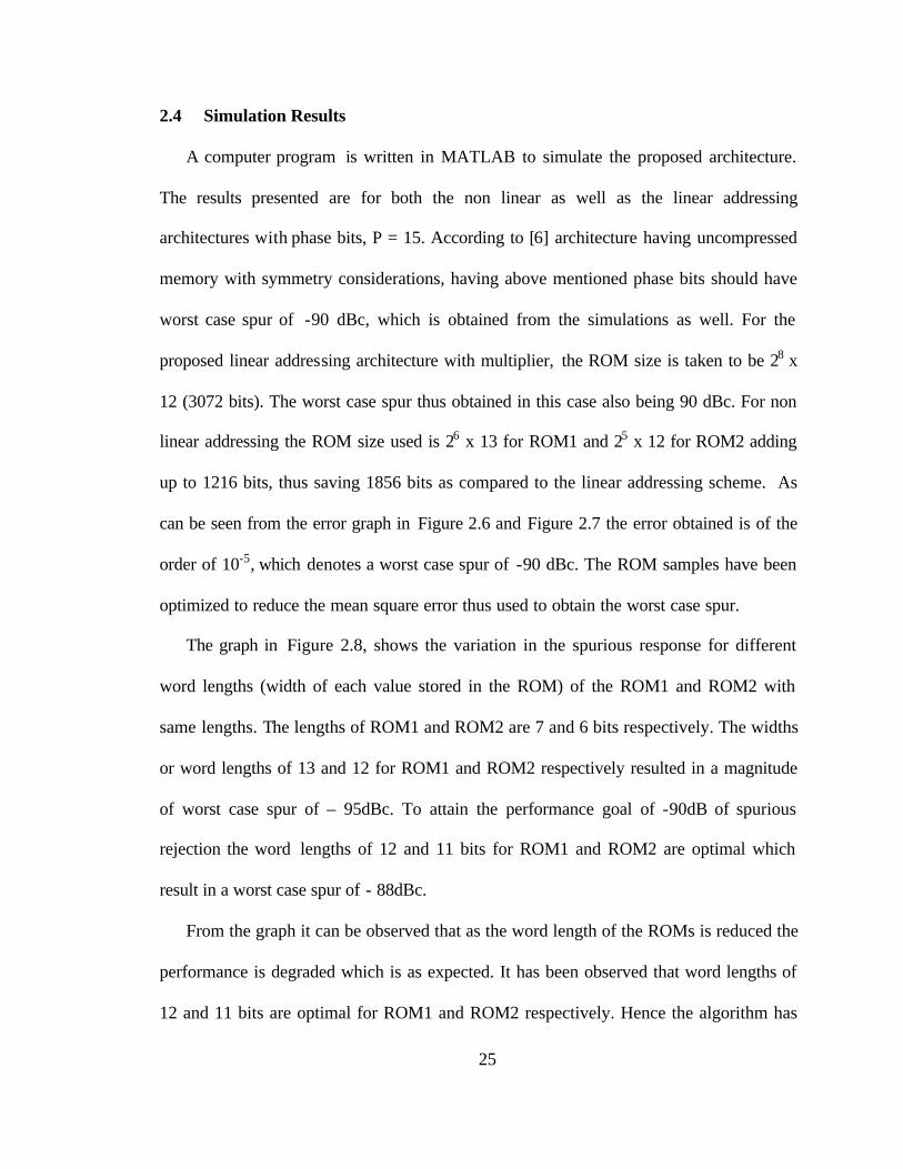
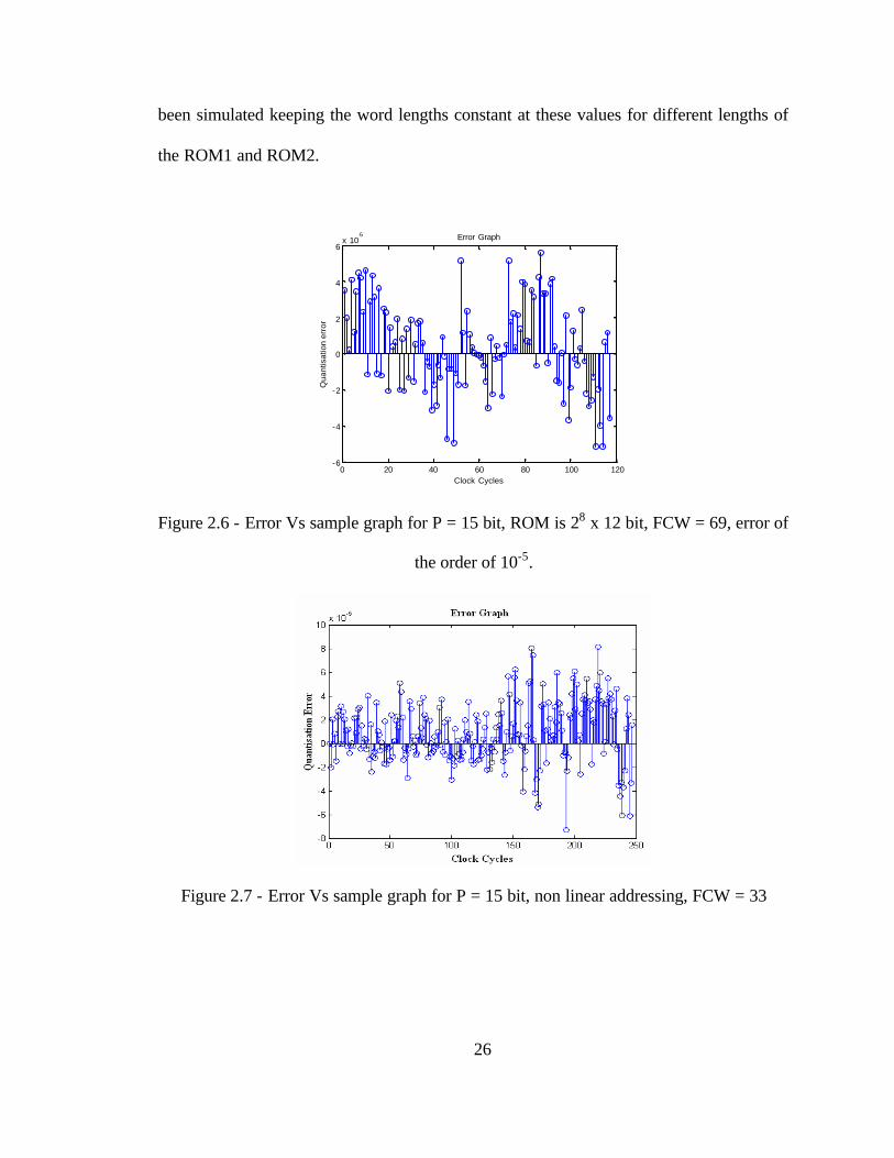
Figure 2.6 and Figure 2.7 show je , which is the error between actual sinusoid
function and that obtained from the proposed architecture for linear and nonlinear
addressing respectively, at each clock cycle. The values of error shown in the graph are
used for calculating the mean of the variance of the error.
25
2.4 Simulation Results
A computer program is written in MATLAB to simulate the proposed architecture.
The results presented are for both the non linear as well as the linear addressing
architectures with phase bits, P = 15. According to [6] architecture having uncompressed
memory with symmetry considerations, having above mentioned phase bits should have
worst case spur of -90 dBc, which is obtained from the simulations as well. For the
proposed linear addressing architecture with multiplier, the ROM size is taken to be 28 x
12 (3072 bits). The worst case spur thus obtained in this case also being 90 dBc. For non
linear addressing the ROM size used is 26 x 13 for ROM1 and 25 x 12 for ROM2 adding
up to 1216 bits, thus saving 1856 bits as compared to the linear addressing scheme. As
can be seen from the error graph in Figure 2.6 and Figure 2.7 the error obtained is of the
order of 10-5, which denotes a worst case spur of -90 dBc. The ROM samples have been
optimized to reduce the mean square error thus used to obtain the worst case spur.
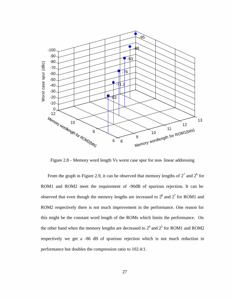
The graph in Figure 2.8, shows the variation in the spurious response for different
word lengths (width of each value stored in the ROM) of the ROM1 and ROM2 with
same lengths. The lengths of ROM1 and ROM2 are 7 and 6 bits respectively. The widths
or word lengths of 13 and 12 for ROM1 and ROM2 respectively resulted in a magnitude
of worst case spur of – 95dBc. To attain the performance goal of -90dB of spurious
rejection the word lengths of 12 and 11 bits for ROM1 and ROM2 are optimal which
result in a worst case spur of - 88dBc.
From the graph it can be observed that as the word length of the ROMs is reduced the
performance is degraded which is as expected. It has been observed that word lengths of
12 and 11 bits are optimal for ROM1 and ROM2 respectively. Hence the algorithm has
26
been simulated keeping the word lengths constant at these values for different lengths of
the ROM1 and ROM2.
0 20 40 60 80 100 120-6
-4
-2
0
2
4
6x 10
-5 Error Graph
Clock Cycles
Qua
ntis
atio
n er
ror
Figure 2.6 - Error Vs sample graph for P = 15 bit, ROM is 28 x 12 bit, FCW = 69, error of
the order of 10-5.
Figure 2.7 - Error Vs sample graph for P = 15 bit, non linear addressing, FCW = 33
27
89
1011
1213
6
8
10
120
-10-20-30-40-50-60-70-80-90
-100
Memory wordlength for ROM1(bits)
Memory wordlength for ROM2(bits)
Wor
st c
ase
spur
(dB
c)-95
-88
-83
-76
-71.2
-63
Figure 2.8 - Memory word length Vs worst case spur for non- linear addressing
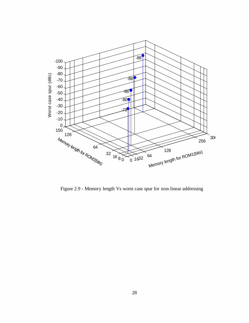
From the graph in Figure 2.9, it can be observed that memory lengths of 27 and 26 for
ROM1 and ROM2 meet the requirement of -90dB of spurious rejection. It can be
observed that even though the memory lengths are increased to 28 and 27 for ROM1 and
ROM2 respectively there is not much improvement in the performance. One reason for
this might be the constant word length of the ROMs which limits the performance. On
the other hand when the memory lengths are decreased to 26 and 25 for ROM1 and ROM2
respectively we get a -86 dB of spurious rejection which is not much reduction in
performance but doubles the compression ratio to 102.4:1.
28
0 1632 64128
256300
081632
64
128150
0-10-20
-30-40-50-60-70-80-90
-100
Memory length for ROM1(bits)
Memory length for ROM2(bits)
Wor
st c
ase
spur
(dB
c)
-88
-88
-86
-80
-71
Figure 2.9 - Memory length Vs worst case spur for non- linear addressing
29
10111213141516
-90
-80
-70
-60
-50
-40
-30
-20
-10
0
Wordlength of ROM in bits
Wor
st c
ase
spur
(dB
c)
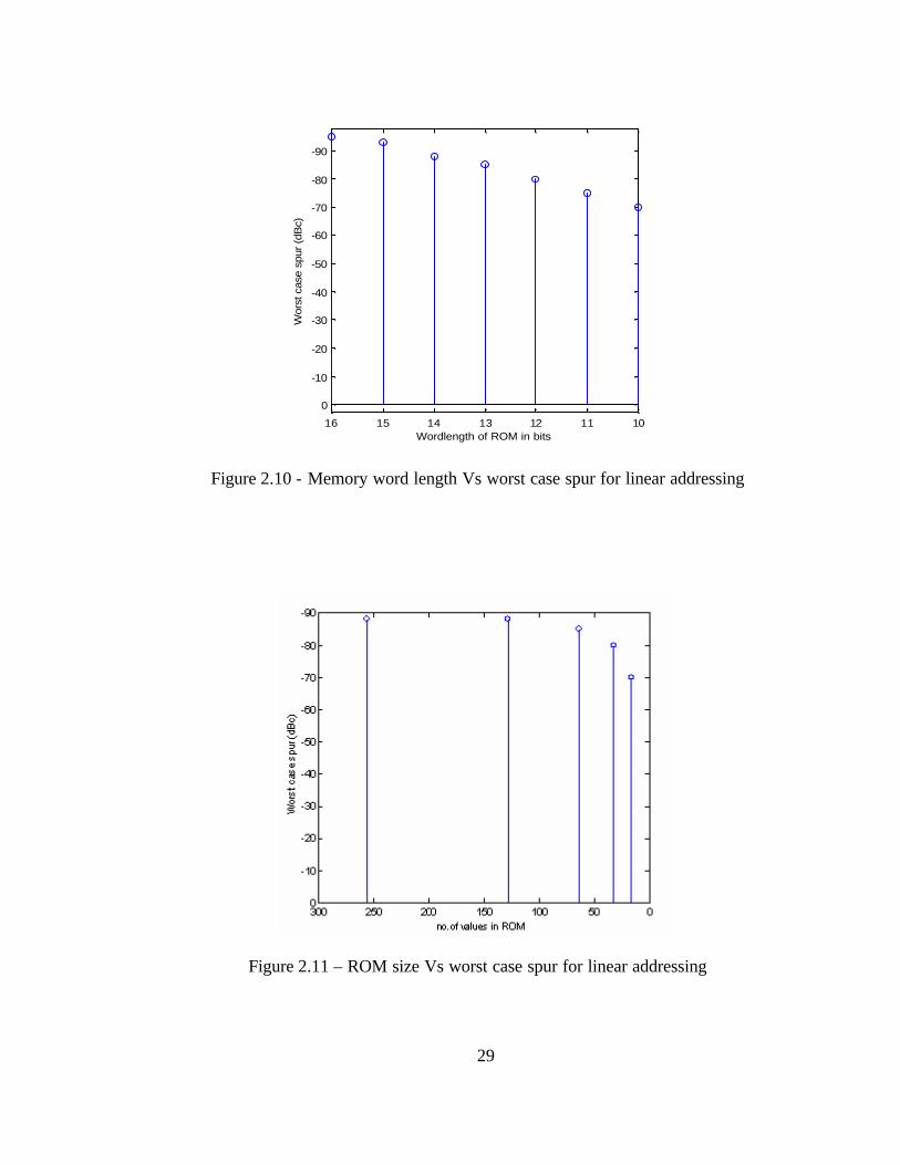
Figure 2.10 - Memory word length Vs worst case spur for linear addressing
Figure 2.11 – ROM size Vs worst case spur for linear addressing
30
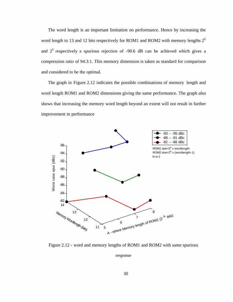
The word length is an important limitation on performance. Hence by increasing the
word length to 13 and 12 bits respectively for ROM1 and ROM2 with memory lengths 26
and 25 respectively a spurious rejection of -90.6 dB can be achieved which gives a
compression ratio of 94.3:1. This memory dimension is taken as standard for comparison
and considered to be the optimal.
The graph in Figure 2.12 indicates the possible combinations of memory length and
word length ROM1 and ROM2 dimensions giving the same performance. The graph also
shows that increasing the memory word length beyond an extent will not result in further
improvement in performance
56
7
8
11
12
13
14-82
-84
-86
-88
-90
-92
-94
-96
A - where Memory length of ROM1 (2A bits)
Wor
st c
ase
spur
(dB
c)
-93 -- -95 dBc-88 -- -91 dBc-82 -- -86 dBc
Memory Wordlength (bits)
ROM1 size=2a x wordlength ROM2 size=2b x (wordlength-1) b=a-1
Figure 2.12 - word and memory lengths of ROM1 and ROM2 with same spurious
response
31
2.5 Conclusion
A novel architecture which exploits the slope of the sine function, for compression of
storage requirement has been proposed. The architecture has been compared with the
existing architectures and the simulation results demonstrated that the same performance
can be achieved with a much better compression ratio. The architectures have also been
implemented using FPGA as described in the following chapter and the results verify the
simulation results.
32
CHAPTER 3
DIRECT DIGITAL SYNTHESIZER - FPGA IMPLEMENTATION
In this chapter the implementation of the novel Direct Digital Frequency Synthesizer
architectures is discussed. Firstly, the design flow in a FPGA is discussed. Further, the
verification of the ROM compression algorithm described in chapter 2 is done by
implementing the architectures using Field Programmable Gate Arrays. The traditional
DDFS architecture with uncompressed ROM, linear architecture and non linear
architecture are coded in Verilog, synthesized using Xilinx Navigator and implemented
on Xilinx Spartan II FPGA.
The output waveform is observed using an oscilloscope and the frequency response is
observed using a spectrum analyzer. The effect of changing the input frequency control
word on the output spectrum is also discussed in detail.
33
3.1 FPGA Design Flow
Field programmable gate arrays were introduced in 1984 as an alternative to
programmable logic devices and application specific ICs. The FPGAs are significantly
programmable and unlike PLDs can be programmed again and again giving the designer
opportunities to fine-tune their circuits. But the downside of FPGA is due to their
availability in only fixed sizes, which matters when avoiding unused silicon area.
FPGAs consist of an array of logic blocks that are configured using software and
programmable I/O blocks surround these logic blocks. Both are connected by
programmable interconnects. The programming technology in an FPGA determines the
type of basic logic cell and the interconnect scheme. In turn the logic cell scheme
determines the design of the input and output circuits.
In the past years the FPGAs have often cost more and could be operated at 40 MHz
maximum but today they cost as less as $10, operate at 300 MHz and also offer
integrated functions like processors and memory.
FPGAs offer all of the features needed to implement most complex designs. Clock
management is facilitated by on-chip PLL (phase locked loop) or DLL (Delay locked
loop) circuitry. Dedicated memory blocks can be configured by blocks like RAMs,
ROMs, FIFOs or CAMs. The ability to link the FPGA with backplanes, high-speed
buses, and memories is afforded by support of various single ended and differential I/O
standards.
Design implementation is done in various steps like design entry or capture, synthesis
and place and route. Design entry is done using the hardware descriptions language
(HDLs). Sometimes it’s also done using schematic based capture tools. In our work we
34
have used the Verilog HDL. HDL is well suited for highly complex designs and basically
depends on the structuring of logic but often it isolates the designer from the hardware
implementation unlike the schematic based entry which gives more visibility into
hardware. We have started our design from a higher level of abstraction than the HDLs,
which is the algorithmic design using MATLAB.
After the design entry the design is simulated at the register-transfer level (RTL). This
is the first step of simulation as the design moves down the simulation hierarchy towards
the physical implementation using FPGA. RTL simulation has the highest speed. At this
stage the variables and signals are observed and consist of well defined functions,
procedures and breakpoints. But at this stage the properties such as the timing and
resource usage are still unknown.
Following RTL simulation a bit stream file is produced using a bit stream converter
which converts the Verilog code into a device netlist format. This file is further converted
to hexadecimal format bit stream file. Lastly this file is loaded into the physical FPGA. A
constraint file is intermediately produced to optimize the netlist. This can be done
globally or to specific portions of the design. This file is given as the input to the
synthesis process as well. Following synthesis the design is placed and routed using
commercial tools. Design rule checking and optimization is performed and the design is
partitioned onto the available logic resources.
Functional simulation follows after synthesis and before implementation for
functional verification.
35
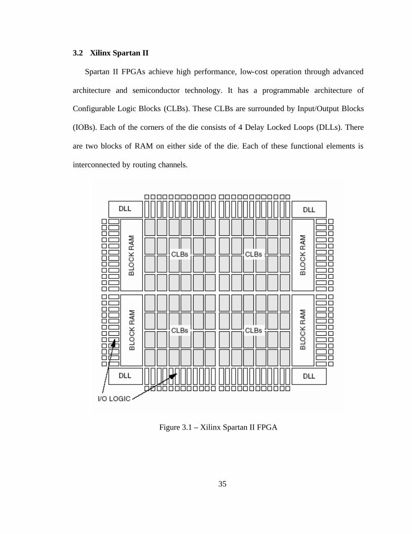
3.2 Xilinx Spartan II
Spartan II FPGAs achieve high performance, low-cost operation through advanced
architecture and semiconductor technology. It has a programmable architecture of
Configurable Logic Blocks (CLBs). These CLBs are surrounded by Input/Output Blocks
(IOBs). Each of the corners of the die consists of 4 Delay Locked Loops (DLLs). There
are two blocks of RAM on either side of the die. Each of these functional elements is
interconnected by routing channels.
Figure 3.1 – Xilinx Spartan II FPGA
36
3.3 Implementation of Proposed Design
We coded the Linear, Nonlinear, and Traditional DDFS architectures using Verilog
RTL and then implemented them in Xilinx Spartan II FPGA. The waveform is observed
using an oscilloscope and the spectrum is observed using a spectrum analyzer. The worst
case spurious response and the carrier-to-noise response are recorded. The results show
similar measurements for the three architectures which verify the conclusion that though
the ROM is compressed in our design the spurious response is not affected. Thus our
architecture for ROM compression produces a high compression ratio with no
degradation in performance.
Due to the PCB board noise at about 30dB, we can only use an 8 bit DAC for our
implementation and therefore have modified the architecture. The accumulator chosen is
of 15 bits. The 15 bit phase word produced is truncated to 9 bits and the remaining 6 bits
are thrown. To optimize the use of the available DAC we have limited the ROM width to
be 8 bits. The 8 bit DAC has about 5~6 effective number of bits that result in about
30~36 dB quantization noise floor as we observed in the test. Thus the worst case
spurious response is 30~36 dBc instead of the expected 48 dBc.
The applied clock frequency is 25 MHz. For frequency control word (FCW) = 1, the
characteristic equation for DDFS gives the output frequency as
HzMf
MHzf
out
clk
93.762)1(2
25
25
15=×=
= (3.1)
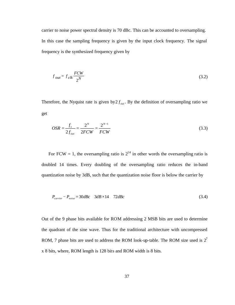
From the spectrum shown, we see the worst case spurious response to be 30 dBc. The
37
carrier to noise power spectral density is 70 dBc. This can be accounted to oversampling.
In this case the sampling frequency is given by the input clock frequency. The signal
frequency is the synthesized frequency given by
2Nclkout
FCWff = (3.2)
Therefore, the Nyquist rate is given by outf2 . By the definition of oversampling ratio we
get
FCWFCWf
fOSR
NN
out
s12
22
2
−
=== (3.3)
For FCW = 1, the oversampling ratio is 214 in other words the oversampling ratio is
doubled 14 times. Every doubling of the oversampling ratio reduces the in-band
quantization noise by 3dB, such that the quantization noise floor is below the carrier by
dBcdBdBcPP noisecarrier 7214330 ≅×+=− (3.4)
Out of the 9 phase bits available for ROM addressing 2 MSB bits are used to determine
the quadrant of the sine wave. Thus for the traditional architecture with uncompressed
ROM, 7 phase bits are used to address the ROM look-up-table. The ROM size used is 27
x 8 bits, where, ROM length is 128 bits and ROM width is 8 bits.
38
Figure 3.2 - Spectrum of the DDFS with a traditional ROM showing the carrier signal and worst case spur for FCW = 1, phase accumulator = 15 bits, DAC resolution = 8 bits,
clock freq. = 25MHz.
39
Figure 3.3 - Spectrum of the DDFS with a traditional ROM showing the carrier signal and quantization noise floor for FCW=1, phase accumulator = 15 bits, DAC resolution =
8 bits, clock freq. = 25MHz.
40
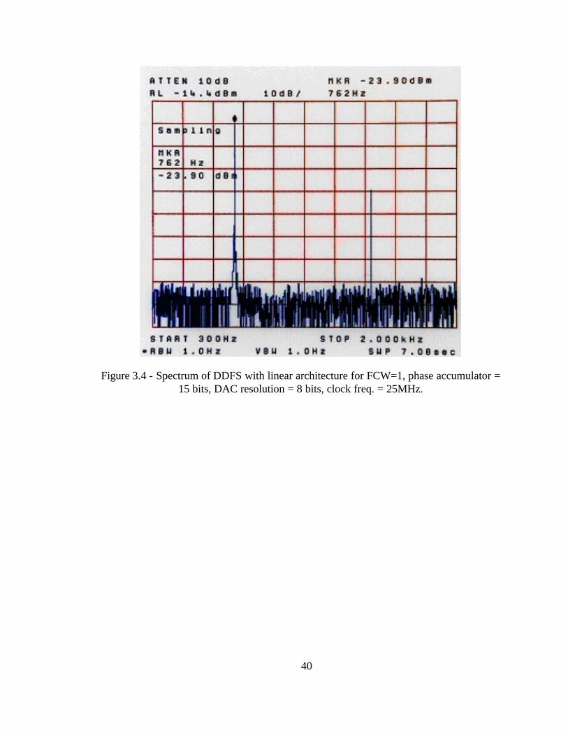
Figure 3.4 - Spectrum of DDFS with linear architecture for FCW=1, phase accumulator =
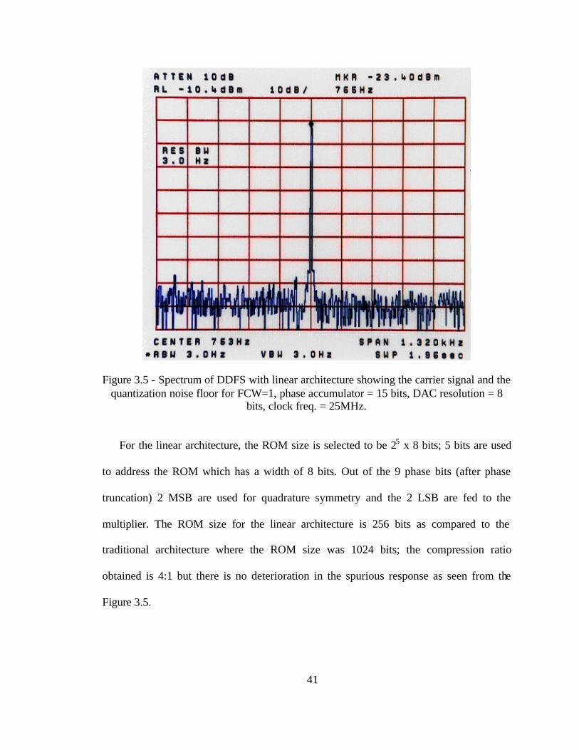
For the linear architecture, the ROM size is selected to be 25 x 8 bits; 5 bits are used
to address the ROM which has a width of 8 bits. Out of the 9 phase bits (after phase
truncation) 2 MSB are used for quadrature symmetry and the 2 LSB are fed to the
multiplier. The ROM size for the linear architecture is 256 bits as compared to the
traditional architecture where the ROM size was 1024 bits; the compression ratio
obtained is 4:1 but there is no deterioration in the spurious response as seen from the
Figure 3.5.
42
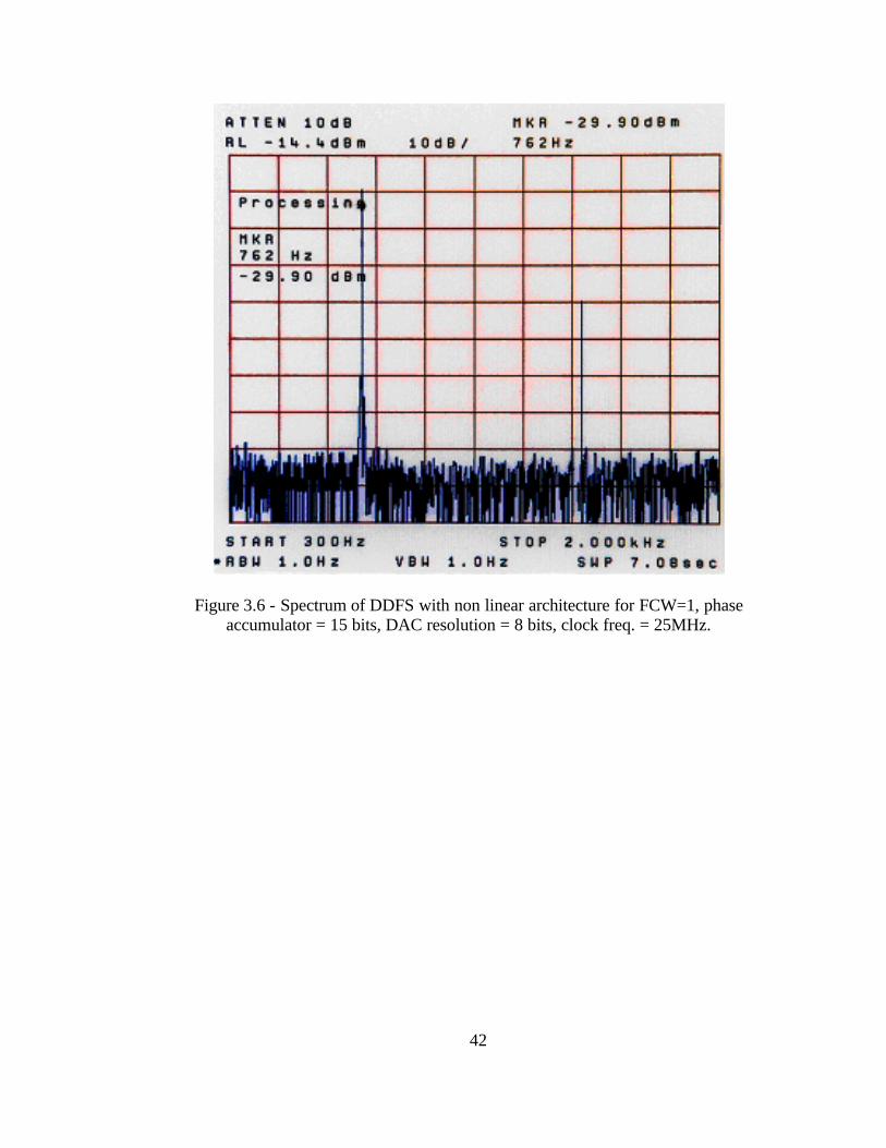
Figure 3.6 - Spectrum of DDFS with non linear architecture for FCW=1, phase accumulator = 15 bits, DAC resolution = 8 bits, clock freq. = 25MHz.
43
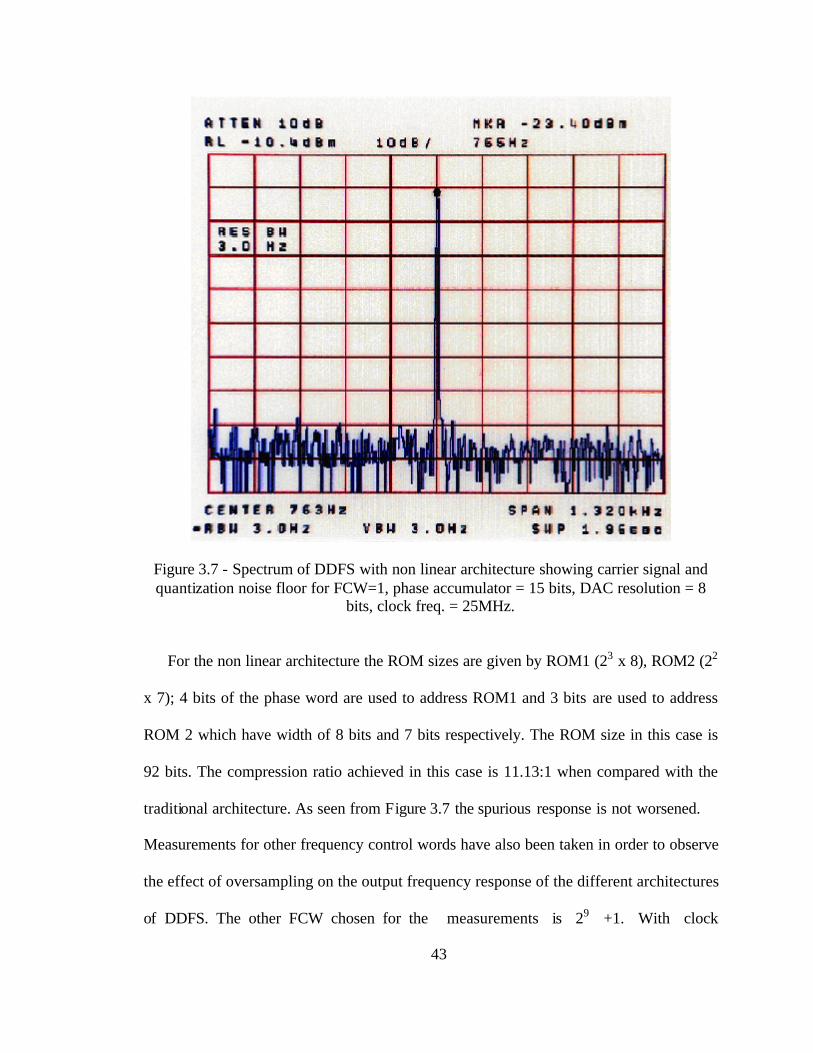
Figure 3.7 - Spectrum of DDFS with non linear architecture showing carrier signal and quantization noise floor for FCW=1, phase accumulator = 15 bits, DAC resolution = 8
bits, clock freq. = 25MHz.
For the non linear architecture the ROM sizes are given by ROM1 (23 x 8), ROM2 (22
x 7); 4 bits of the phase word are used to address ROM1 and 3 bits are used to address
ROM 2 which have width of 8 bits and 7 bits respectively. The ROM size in this case is
92 bits. The compression ratio achieved in this case is 11.13:1 when compared with the
traditional architecture. As seen from Figure 3.7 the spurious response is not worsened.
Measurements for other frequency control words have also been taken in order to observe
the effect of oversampling on the output frequency response of the different architectures
of DDFS. The other FCW chosen for the measurements is 29 +1. With clock
44
frequency of 25 MHz we have the synthesized output frequency of the DDFS given by
KHz
Mf
MHzf
out
clk
38.391)12(2
25
25
915 =+×=
= (3.5)
The oversampling ratio is given by
59
14
222
2=≈=
out
s
ff
OSR (3.6)
Therefore by definition of oversampling the carrier-to-noise ratio is given by
dBcdBdBcPP noisecarrier 455330 ≅×+=− (3.7)
As seen from the following figures, the carrier to noise ratio is 45~50 dBc. However
the worst case spurious response remains 30 dBc and does not depend on the frequency
control word. The following Figures show the frequency response of all the three DDFS
architectures when FCW is chosen to be 29 +1. The frequency response of the DDFS
output shows that the quantization noise floor gets raised by about 25 dB, such that it
almost covers the harmonic tones.
45
Figure 3.8 - Spectrum of DDFS with a traditional ROM for FCW = 29 +1, phase accumulator = 15 bits, DAC resolution = 8 bits, clock freq. = 25MHz
Figure 3.9 - Spectrum of DDFS with linear architecture for FCW = 29 +1, phase accumulator = 15 bits, DAC resolution = 8 bits, clock freq. = 25MHz
46
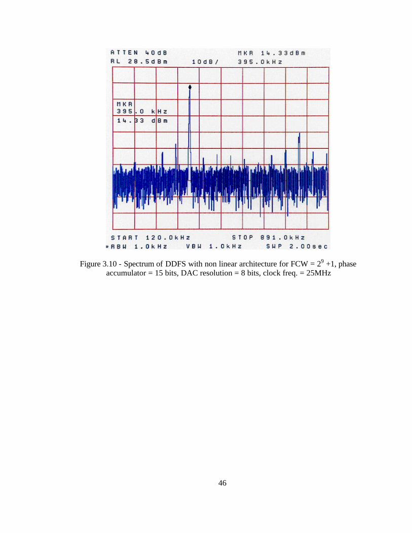
Figure 3.10 - Spectrum of DDFS with non linear architecture for FCW = 29 +1, phase accumulator = 15 bits, DAC resolution = 8 bits, clock freq. = 25MHz
47
3.4 Conclusion
Due to the presence of board noise only an 8 bit DAC is used for the DDFS
implementation. The truncation of the phase output of the accumulator is done in order to
effectively size the ROM to optimize the use of the available DAC. The observed
reduction of the compression ratio for linear and non linear architectures is due to the
small ROM look up table size selected due to implementation constraints. From the
measurements obtained, we see same spurious performance achieved in the linear and
non linear DDFS architectures with significant ROM compression when compared to the
traditional uncompressed ROM, DDFS architecture. We have also taken measurements
for different frequency control words like FCW = 29 + 1, and have analyzed the effect of
oversampling on the frequency response
48
CHAPTER 4
SIGMA DELTA MODULATOR FOR HIGH SPEED ROMLESS DDFS
Tierney et al. [1] originally introduce the architecture of a conventional DDFS. As
shown in chapter 2, Figure 2.1 the basic building blocks consist of a phase accumulator, a
phase-to-sine amplitude ROM look-up-table and a linear DAC. The phase accumulator
addresses the ROM look-up-table, which converts the phase information into the values
of sine wave. The linear DAC [18] is used to convert the quantized sine wave into analog
voltage. Large ROM and high resolution DAC are usually required to improve the
spectral purity of a sine wave output. However, a larger ROM means higher power
consumption, slower access time and large die area [19][20]. We made an effort in this
work to present a DDFS architecture using a non- linear DAC in place of the ROM look-
up-table and linear DAC. Most Direct Digital Frequency Synthesizers utilize an
overflowing accumulation to generate desired frequencies. In our design a conventional
phase accumulator generates instantaneous phase values, and the sine weighted DAC
maps the phase values to the corresponding sine amplitudes. Realizing this architecture in
circuitry causes spurious noise. To maintain reasonable hardware complexity of the
DAC, bit truncation of phase output is done. This reduces the DAC size but produces
truncation errors. The output of a conventional phase accumulator is a ramp function with
periodic overflow. Due to this nature of phase accumulators and the nature of DDFS
49
mechanism the truncation error thus produced becomes periodic, causing undesired
harmonic tones in the output spectrum. These spurious harmonic tones are known as the
spurs. There are two major causes of spurs in DDFS output spectrum:
1) Phase truncation and
2) Amplitude quantization.
In this chapter we are basically dealing with the phase truncation effect. The spectral
purity of the output signal can be improved significantly if the periodicity of the truncated
bits can be removed and thus the power of the spurs can be reduced. In the past to
eliminate data pattern periodicity techniques like dithering have been used. These random
jittering techniques produce an additional f/1 noise. We have chosen the sigma delta
modulation as the spur reduction technique as it randomizes the signal just like the
jittering techniques but is devoid of the f/1 noise. The results show that sigma delta
reduces the spurs arising from the phase truncation.
50
4.1 Analysis of DDFS Output
In traditional DDFS as mentioned above an overflowing accumulation of the
Frequency Control Word (FCW) is done to produce phase values. Increasing the number
of bits in the phase accumulator thus provides more accurate frequency control and
higher frequency resolution. In the equation shown below ]1[ +nφ gives the phase output
obtained at sample ]1[ +n . M represents the length of the accumulator in bits.
MFCWnn 2mod)][(]1[ +=+ φφ (4.1)
The major trade off to these advantages is the added circuit complexity and increased
hardware. Thus phase bit truncation becomes indispensable. But this further leads to
phase truncation noise which restricts the SFDR determined by 6.02 x L dB, where L
determines the number of bit being fed into the phase to sine converter and thus (M-L)
represents the truncated bits. Equation 4.2 gives the truncation error that can be obtained
as
LMRnn −+=+ 2mod)][(]1[ ϕϕ (4.2)
R here represents the value of the thrown away, least significant bits of the frequency
control word and is given by
LMLM
FCWFCWR −
− ×
−= 2
2 (4.3)
51
Therefore, an error feedback technique involving the second order sigma delta
modulator is proposed [23][24] such that the extra bits that are being thrown away can be
utilized to improve the SFDR.
In this work a second order Σ∆ modulator which realizes the transfer function of
2-1z2 −−⋅ z which provides a noise shaping of 40dB/decade. The results verify that the
Sigma Delta modulator as used in the architecture increases the out of band quantization
noise and reduces the in band spurs arising from phase truncation by its noise shaping
property and thus enhances the spectral purity [25][26]. In this work we verify the noise
shaping action of the chosen architecture of sigma- delta modulator using Simulink /
MATLAB and then go on to implement in CADENCE. The time sequence simulations
from MATLAB have been bit-by-bit compared with the CADENCE time sequence
simulations and thus the Σ∆ architecture implementation has been verified.
4.2 Introduction to Sigma-Delta Theory
In 1954, a patent was filed by Cutler, of a feedback system with a low-resolution
quantizer in the forward path. The quantization error of a quantizer was fed back and
subtracted from the input signal. The principle of improving the resolution of a coarse
quantizer by use of feedback is the basic concept of a delta-sigma converter. In 1962,
Inose came up with the idea of adding a filter in the forward path of the well-known delta
modulator in front of the quantizer. This system was called a delta – sigma modulator
where delta refers to the delta–modulator and sigma refers to summation by the
integrator.
52
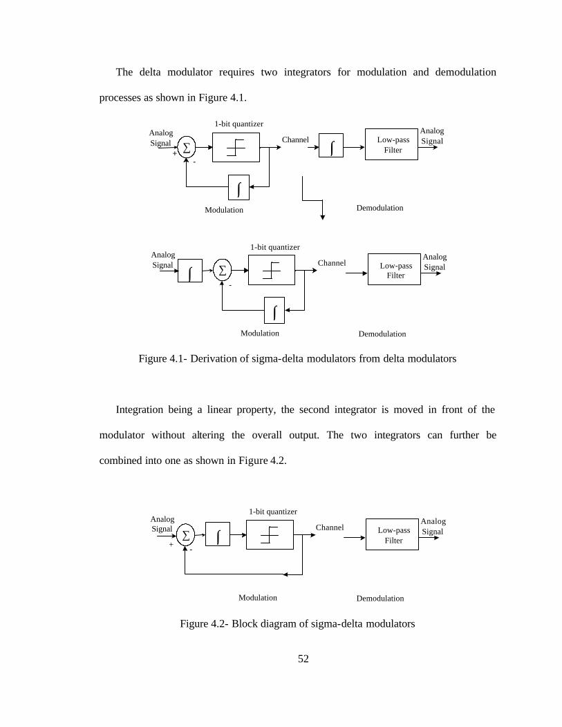
The delta modulator requires two integrators for modulation and demodulation
processes as shown in Figure 4.1.
+
1-bit quantizerAnalogSignal
-
∫
∑ ∫Low-pass
Filter
AnalogSignalChannel
Modulation Demodulation
1-bit quantizerAnalogSignal
-
∫
∑Channel
Modulation
∫Low-pass
Filter
AnalogSignal
Demodulation
Figure 4.1- Derivation of sigma-delta modulators from delta modulators
Integration being a linear property, the second integrator is moved in front of the
modulator without altering the overall output. The two integrators can further be
combined into one as shown in Figure 4.2.
1-bit quantizerAnalogSignal
-
∑Channel
Modulation
∫ Low-passFilter
AnalogSignal
Demodulation
+
Figure 4.2- Block diagram of sigma-delta modulators
53
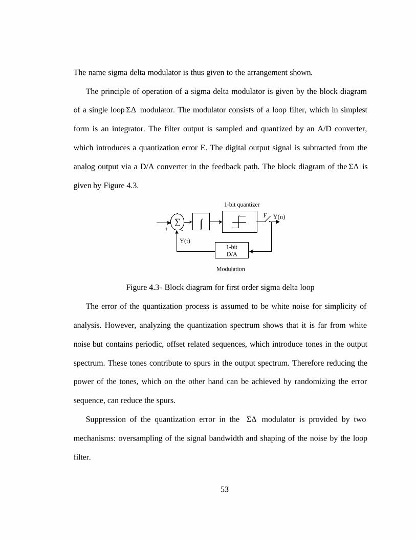
The name sigma delta modulator is thus given to the arrangement shown.
The principle of operation of a sigma delta modulator is given by the block diagram
of a single loop Σ∆ modulator. The modulator consists of a loop filter, which in simplest
form is an integrator. The filter output is sampled and quantized by an A/D converter,
which introduces a quantization error E. The digital output signal is subtracted from the
analog output via a D/A converter in the feedback path. The block diagram of the Σ∆ is
given by Figure 4.3.
Y(n)
1-bit quantizer
-∑
Modulation
∫+
1-bitD/A
Y(t)
F
Figure 4.3- Block diagram for first order sigma delta loop
The error of the quantization process is assumed to be white noise for simplicity of
analysis. However, analyzing the quantization spectrum shows that it is far from white
noise but contains periodic, offset related sequences, which introduce tones in the output
spectrum. These tones contribute to spurs in the output spectrum. Therefore reducing the
power of the tones, which on the other hand can be achieved by randomizing the error
sequence, can reduce the spurs.
Suppression of the quantization error in the Σ∆ modulator is provided by two
mechanisms: oversampling of the signal bandwidth and shaping of the noise by the loop
filter.
54
4.2.1 Oversampling
A one bit quantizer generates a bitstream pattern with output levels 2/q± , where q is
the quantization step size. The bitstream spectrum contains information about the input
signal and a quantization error, which is introduced by the quantizer [27].
Assuming the quantizer to have a white noise spectrum and the total power of the
quantization error signals equals
12/22 qerms = (4.4)
The power spectral density of the sampled quantization error signal is
2/0,6/)( 2
ss fffqfE ≤≤= (4.5)
where sf is the sampling frequency. This equation shows the relation between the
quantization noise power and sampling frequency. It shows higher the sampling
frequency, the lower the noise power density. This is the principle of oversampling. The
integrated noise power within a fixed signal bandwidth decreases if the sampling rate is
increased. The total in-band quantization noise power equals
me
dffEN rmf
q
b 2
0
)( == ∫ (4.6)
where bf is the signal bandwidth. The oversampling ratio m is the ratio between the
sampling frequency and the Nyquist bandwidth (twice the signal bandwidth)
55
b
s
ff
m2
= (4.7)
4.2.2 Noise-shaping
For low frequency signals, the DAC in the feedback path has a gain of approximately
1. The Figure shows a highly linear model of a basic Σ∆ modulator. Using this model,
the output Y(s) of the Σ∆ modulator is determined to be
)(.)(1
1)(.
)(1)(
)( sNsH
sXsH
sHsY
++
+= (4.8)
where X(s) is the analog input signal and H(s) is the loop filter transfer function. The first
term of the right is the signal transfer function (STF) and the second term is the noise
transfer function (NTF).
Considering the loop filter to be a simple integrator; the loop filter transfer function
H(s) becomes equal tos1
. Therefore the signal transfer function (STF) is given by
ssXsY
sXs
sX
s
ssY
+=
+=
+=
11
)()(
)(1
1)(
11
1
)(
(4.9)
The above signal transfer function resembles that of a low pass filter. Thus if H(s) has a
low pass filter characteristics with high DC gain, then for low-frequencies the signal
transfer function is close to 1, while the quantization error tends toward zero(NTF
56
is 0).
For frequencies close to half the sampling frequency, the input signal is filtered and
the quantization error becomes large. Considering X(s) = 0, this can be mathematically
denoted as
111
1)()(
)(1
)()(
+=
+=
+−=
ss
ssNsY
sNs
sYsY
(4.10)
Thus the noise transfer function resembles that of a high pass filter. This shows that
the quantization noise density function is not constant over frequency, but has a shaped
frequency spectrum. As the loop integrates the error between the sampled signal and the
input signal, it low pass filters the signal and high-pass filters the noise. In other words,
the signal is left unchanged as long as its frequency content doesn’t exceed the filters
cutoff frequency, but the Σ∆ loop pushes the noise into a higher frequency band.
Oversampling the input causes the quantization noise to spread over a wide bandwidth
and the noise density in the bandwidth of interest to significantly decrease. This is the
principle of noise shaping.
4.2.3 Analysis of Delta Sigma Modulator in z Domain
The z domain transfer function of the integrator can be denoted as I (z) such that for
an ideal integrator
57
11
1)(
−−=
zzI (4.11)
The standard discrete time signal analysis yields
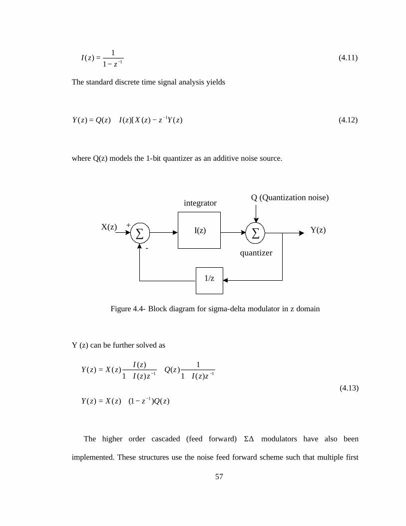
)()()[()()( 1 zYzzXzIzQzY −−+= (4.12)
where Q(z) models the 1-bit quantizer as an additive noise source.
Q (Quantization noise)
Y(z)
quantizer
integrator
1/z
X(z) +
-
I(z)∑ ∑
Figure 4.4- Block diagram for sigma-delta modulator in z domain
Y (z) can be further solved as
)()1()()(
)(11
)()(1)(
)()(
1
11
zQzzXzY
zzIzQ
zzIzI
zXzY
−
−−
−+=
++
+=
(4.13)
The higher order cascaded (feed forward) Σ∆ modulators have also been
implemented. These structures use the noise feed forward scheme such that multiple first
58
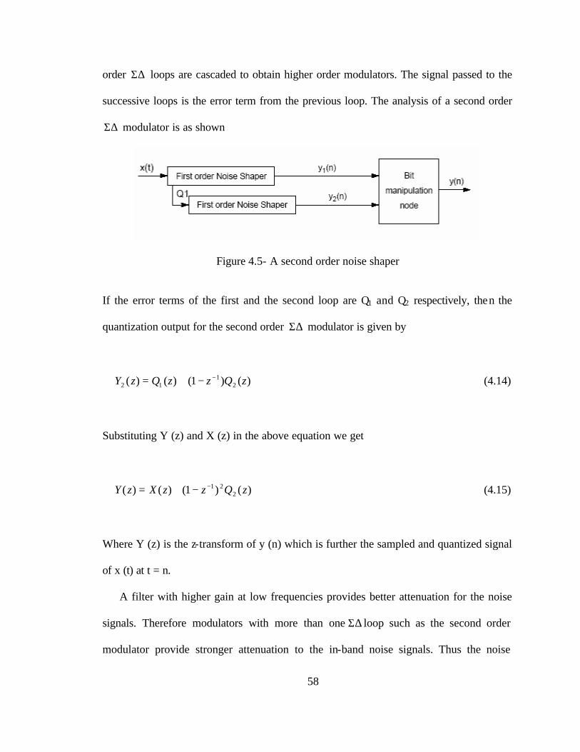
order Σ∆ loops are cascaded to obtain higher order modulators. The signal passed to the
successive loops is the error term from the previous loop. The analysis of a second order
Σ∆ modulator is as shown
Figure 4.5- A second order noise shaper If the error terms of the first and the second loop are Q1 and Q2 respectively, then the
quantization output for the second order Σ∆ modulator is given by
)()1()()( 21
12 zQzzQzY −−+= (4.14)
Substituting Y (z) and X (z) in the above equation we get
)()1()()( 221 zQzzXzY −−+= (4.15)
Where Y (z) is the z-transform of y (n) which is further the sampled and quantized signal
of x (t) at t = n.
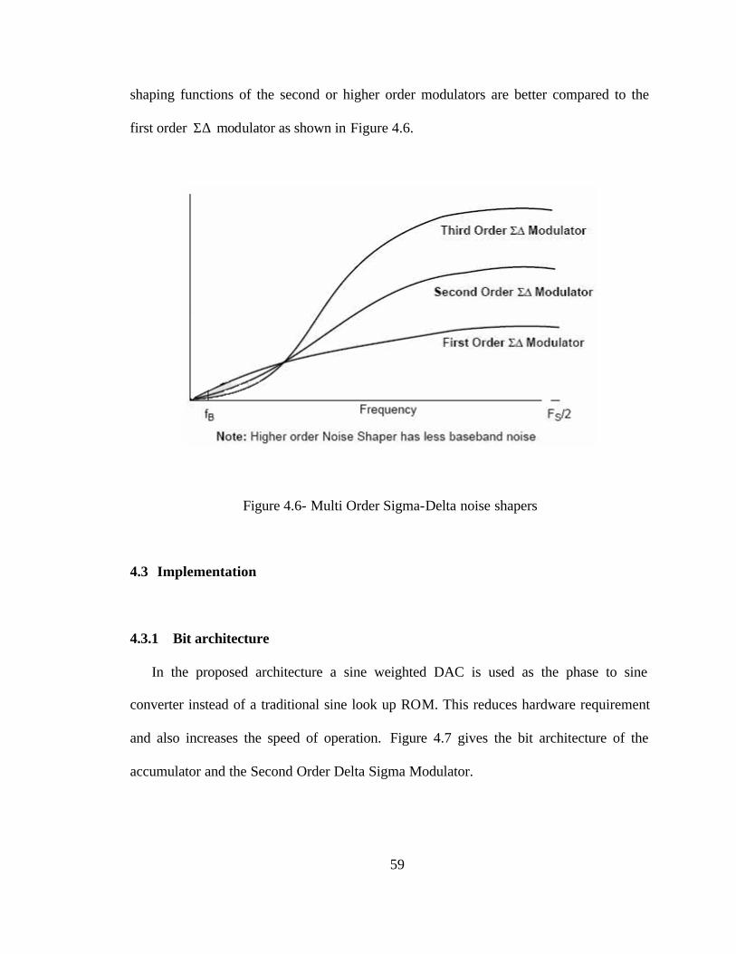
A filter with higher gain at low frequencies provides better attenuation for the noise
signals. Therefore modulators with more than one Σ∆ loop such as the second order
modulator provide stronger attenuation to the in-band noise signals. Thus the noise
59
shaping functions of the second or higher order modulators are better compared to the
first order Σ∆ modulator as shown in Figure 4.6.
Figure 4.6- Multi Order Sigma-Delta noise shapers
4.3 Implementation
4.3.1 Bit architecture
In the proposed architecture a sine weighted DAC is used as the phase to sine
converter instead of a traditional sine look up ROM. This reduces hardware requirement
and also increases the speed of operation. Figure 4.7 gives the bit architecture of the
accumulator and the Second Order Delta Sigma Modulator.
60
Figure 4.7- Block diagram showing bit architecture of the implemented Σ∆ modulator
The proposed architecture utilizes an 8-bit accumulator thus producing 8-bit phase
word. The output of the modulator is also 8 bit. This when combined with the phase word
produces 9 bit output where the carry bit is neglected and the MSB 6 bits are fed to the
sine weighted DAC and LSB 2 bits are given as input to the Σ∆ modulator.
4.3.2 MATLAB Simulation and Verification
Simulink is used to generate a Σ∆ modulator realizing the equation 2-12 −− zz as
shown in the figure. Here unit delay is represented by the z1
block. The user defined
function blocks take care of the bit truncations required. The input given to the blocks is
of 8 bits which when passed through the truncation 2 block introduces the LSB 2 bits to
the Σ∆ modulator. Similarly, the 8 bits when passed through the truncation 6 bits block
introduces MSB 6 bits to the successive block, which is a sine weighted DAC in the
implementation but here is a scope to observe the action of Σ∆ modulator. A
61
sinusoidal input is introduced in the modulator to understand its noise shaping behavior.
This is because the spectrum of a sinusoid is an impulse at the sine input frequency and
can be better observed as opposed to the spectrum of the staircase function (output of
conventional phase accumulator) whose exact nature is difficult to analyze. The sine
input frequency here is specified to be 1 Hz and can be clearly observed in the noise
shaping simulation output.
Once the noise shaping behavior is observed and Σ∆ modulation is verified, an
accumulator is attached to the Σ∆ modulator block. This has been done in both structural
and behavioral method to further verify the simulation results. In the behavioral
simulation, the modulator block is given by a discrete transfer function block, which
specifies the desired equation; whereas in the structural model the equation has been
realized using different constituting blocks. Both the models give the same simulation
results. The user defined function block f(u) in the phase accumulator of the model takes
care of the overflow of the accumulator and starts from 0 once the accumulator reaches
28-1 i.e. 255
62
Figure 4.8- Second order sigma delta modulator with sinusoidal input
Figure 4.9- Spectrum obtained for sinusoidal input to second order Sigma Delta modulator. The graph shows 40dB noise shaping.
63
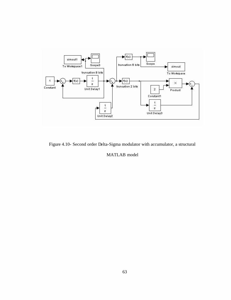
Figure 4.10- Second order Delta-Sigma modulator with accumulator, a structural
MATLAB model
64
4.3.3 CADENCE Simulation
Top-level design
The top- level design consists of an 8-bit accumulator block, which is designed
behaviorally using Verilog A. The design has been implemented in differential output
form. The output of the accumulator is given to the sigma-delta modulator block. The
design is biased at 3 V and refV is chosen to be 1.1V. EEV and substrate is grounded. The
clock given to the module is biased at 2.8V. The MSB 6 bits of the Σ∆ modulator output
are further fed to the next module which is the DAC (not shown in the top level). The
differential output of the delta-sigma modulator block is fed to the 6 parallel Master-
Slave flip-flops to remove any glitches, which might be present in the output signal for
the ease of analysis and verification. The differential output thus obtained from the flip-
flops is further converted into single mode binary output using the behavioral
comparators, designed in Verilog A. The comparators are referenced at 0 and the output
is obtained in terms of 1’s or 0’s.
Accumulator
The accumulator has been designed behaviorally using the functional library of the
CADENCE tool. The specifications of the design are given in Verilog A. The 8-bit phase
accumulator is designed with a concept that the frequency of the MSB is 2÷ of that of
the 2nd MSB; whose frequency again is 2÷ of that of the 3rd MSB such that the LSB has
the highest frequency. But the frequency of the LSB is maintained to be 2÷ of the clock
frequency.
65
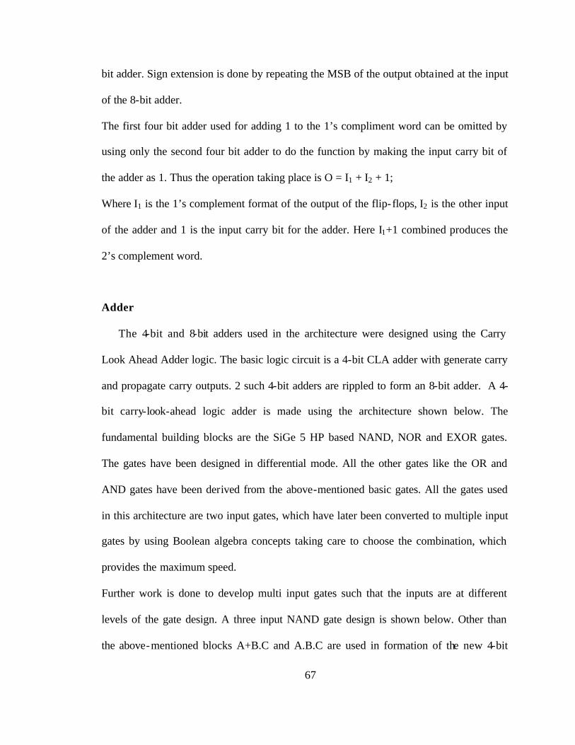
This is implemented using the behavioral D flip-flops, which bring about the
frequency division-by-2. Thus the output signal of every D flip-flop has a frequency of
half of its input signal. The output Q gives the positive terminal for the output bit and Q-
is fed to the clock input of the next D flip-flop and also gives the negative terminal of the
output bit as shown. Q-output of every D flip-flop is also fed back as the D input of the
flip-flop to implement the divided-by-2 circuit. LSB is given by the first D flip-flop
output whose frequency is half of the clock frequency; MSB is given by the output of the
8th flip-flop from the left and has a frequency of 256÷ of that of the clock frequency.
When these bits were added after converting the differential output to single mode binary
output using comparators we could observe the characteristic staircase output of the
phase accumulator.
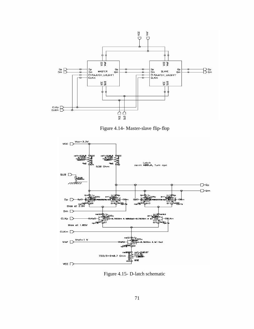
D flip-flop (Master-slave flip-flop)
The D flip-flop is designed by combining two D latch modules in master-slave
configuration such that the clock is given directly to the master D latch and is inverted
and given to the slave D latch. The D latch is designed using the differential CML logic
with tail current of approximately 400µA. The clock and the D inputs are biased at 1.9V
and 2.9V respectively. The D flip-flops designed for this architecture are rising edge
triggered and have no reset.
66
Delta-sigma Modulator
The first block of the Σ∆ modulator is the 8-bit adder. The input of the adder consists
of the phase bits produced by the accumulator and the bits fed back by the Σ∆
modulator. The output carry bit of the adder is neglected and the input carry bit is
maintained to be 0. The MSB 6 bits are fed as input to the DAC and the LSB two bits are
given as input to the Σ∆ modulator. Σ∆ Modulator consists of the master-slave flip-flops
connected in parallel- in-parallel-out configuration to implement 1−z . As mentioned above
the Σ∆ modulator architecture used has a transfer function given by 2-1z2 −−⋅ z .
The 12 −z or 2× is realized using left shift-by-1 concept, such that a 0 is placed at the
LSB bit when the other bits are shifted to the left by one bit. Subtraction is done using 2’s
complement method; such that the 1’s complement is produced by inverting the
differential inputs to the adder and then adding 1 to it. The first four bit adder is used to
obtain the 2’s compliment of the output of the flip-flops; thus producing 1−− Az , where A
is the input to the modulator given by the 2 LSBs. This is then is further added to A2 by
the second 4 bit adder. Since the 2 bit input to the Σ∆ modulator becomes three bit after
the left shift operation and also because the other input to the adder is in 2’s compliment
format which requires sign expansion we are using a 4 bit adder instead of a 3 bit adder.
The carry of the adder is always neglected by the rule of 2’s compliment binary
operations. The transfer function at this point is given by Az )2( 1−− . This one passing
through another set of parallel flip- flops produces the desired transfer function 212 −− − zz .
The output thus produced from the Σ∆ modulator is 4 bit and in 2’s compliment format.
Therefore to pack the bits correctly we do sign extension of the output MSB such that the
four-bit output is sign extended to 8-bit output. This is fed back as input to the 8-
67
bit adder. Sign extension is done by repeating the MSB of the output obtained at the input
of the 8-bit adder.
The first four bit adder used for adding 1 to the 1’s compliment word can be omitted by
using only the second four bit adder to do the function by making the input carry bit of
the adder as 1. Thus the operation taking place is O = I1 + I2 + 1;
Where I1 is the 1’s complement format of the output of the flip-flops, I2 is the other input
of the adder and 1 is the input carry bit for the adder. Here I1+1 combined produces the
2’s complement word.
Adder
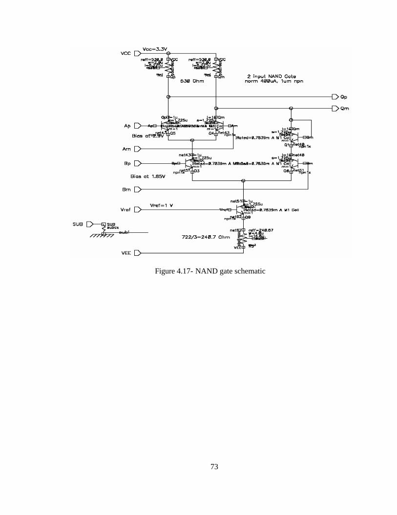
The 4-bit and 8-bit adders used in the architecture were designed using the Carry
Look Ahead Adder logic. The basic logic circuit is a 4-bit CLA adder with generate carry
and propagate carry outputs. 2 such 4-bit adders are rippled to form an 8-bit adder. A 4-
bit carry-look-ahead logic adder is made using the architecture shown below. The
fundamental building blocks are the SiGe 5 HP based NAND, NOR and EXOR gates.
The gates have been designed in differential mode. All the other gates like the OR and
AND gates have been derived from the above-mentioned basic gates. All the gates used
in this architecture are two input gates, which have later been converted to multiple input
gates by using Boolean algebra concepts taking care to choose the combination, which
provides the maximum speed.
Further work is done to develop multi input gates such that the inputs are at different
levels of the gate design. A three input NAND gate design is shown below. Other than
the above-mentioned blocks A+B.C and A.B.C are used in formation of the new 4-bit
68
adder. Here A, B, C represent the three input signals. The generation of the CLA can be
given by the following equations.
])()[()}](){()[(4
)}](){()[(3
)()(2
1
001230123123233
001012122
001011
000
cppppgpppgppgpgc
cppgppgpgc
cppgpgc
cpgc
⋅⋅⋅⋅+⋅⋅⋅+⋅⋅+⋅+=
⋅⋅+⋅⋅+⋅+=
⋅⋅++=
+=
For this architecture two level shifters, shifting voltage levels from 3.3V to 2.2 V and 2.2
V to 1.3V are required. Overall the number of level shifters is reduced when the multiple
input gates are used. This architecture also reduces the delay period for the 4-bit adder.
69
Figure 4.11- Top level of the implemented design with 8 bit behavioral accumulator, delta-sigma modulator block, 6 bit output passing through parallel master-slave flip flips
and comparators to obtain bitwise output.
70
Figure 4.12- Behavioral accumulator used in the design
Figure 4.13- Delta-sigma modulator block
71
Figure 4.14- Master-slave flip-flop
Figure 4.15- D-latch schematic
72
Figure 4.16- 4-bit adder realization using gates
73
Figure 4.17- NAND gate schematic
74
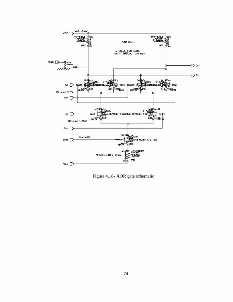
Figure 4.18- XOR gate schematic
75
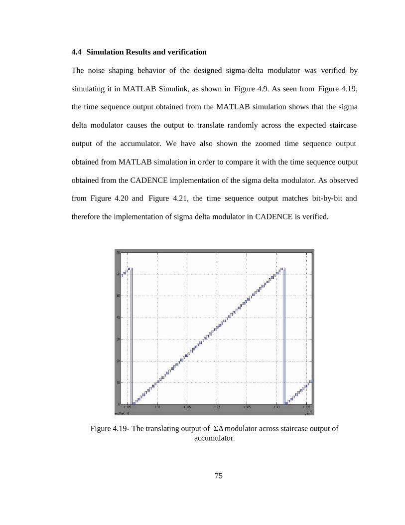
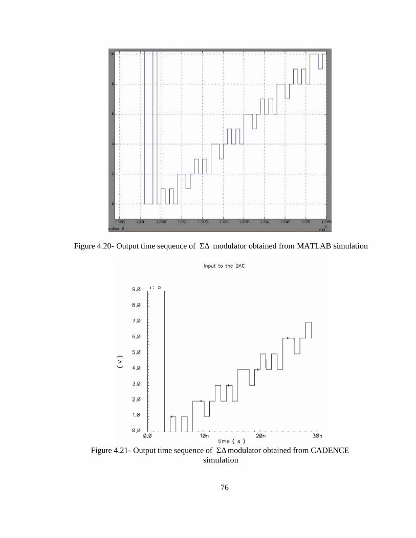
4.4 Simulation Results and verification
The noise shaping behavior of the designed sigma-delta modulator was verified by
simulating it in MATLAB Simulink, as shown in Figure 4.9. As seen from Figure 4.19,
the time sequence output obtained from the MATLAB simulation shows that the sigma
delta modulator causes the output to translate randomly across the expected staircase
output of the accumulator. We have also shown the zoomed time sequence output
obtained from MATLAB simulation in order to compare it with the time sequence output
obtained from the CADENCE implementation of the sigma delta modulator. As observed
from Figure 4.20 and Figure 4.21, the time sequence output matches bit-by-bit and
therefore the implementation of sigma delta modulator in CADENCE is verified.
Figure 4.19- The translating output of Σ∆ modulator across staircase output of accumulator.
76
Figure 4.20- Output time sequence of Σ∆ modulator obtained from MATLAB simulation
Figure 4.21- Output time sequence of Σ∆ modulator obtained from CADENCE
simulation
77
4.5 Conclusion
The speed of the Σ∆ modulator though is limited by the speed of the adder, which is
found to be of 6GHz. Since in the Σ∆ module has the longest delay path contains 2
adders; 8 bit adder and 4 bit adder the speed obtained is 3Ghz approximately. The rest of
the block are connected in pipeline and thus do not affect the speed. The current and
power consumption of the sigma delta block was calculated to be 139.5 mA and 460.35
mW respectively. The following is the gates count description and the estimated layout
”CMOS/SOS frequency synthesizer LSI circuit for spread spectrum communications“, IEEE J Solid-State Circuits, vol. 19 Issue 4 , pp 497 -506, Aug 1984.
[5] H. T. Nicholas, et al., “The optimization of direct digital frequency synthesizer
performance in the presence of finite word length effects,” Proc. 42nd Annual Frequency Control Symp. USERACOMM (Ft. Monmouth, NJ), May 1988, pp. 357-363
[6] H.T. Nicholas III and H.Samueli,“A 150 MHz direct digital frequency synthesizer
in 1.25 um CMOS with -90dBc Spurious Performance,” IEEE J. Solid-State Circuits, vol. 26, pp. 1959-1969, Dec. 1991.
[7] F. Curticapean and J. Niittylahti, “Low-power direct digital frequency
synthesizer,” proc. IEEE 43rd Midwest symposium on Circuits and Systems, 2000, on CD-ROM.
[8] A. Bellaouar, M. Obrecht, A. Fahim, and M.I. Elmasry, “A low-power direct
digital frequency synthesizer architecture for wireless communications,” IEEE J. Solid-State Circuits, vol. 35, pp 385-390, March 2000.
[9] M.M. El Said, M.I. Elmasry, “An improved ROM compression technique for
direct digital frequency synthesizers”, Proc. of IEEE Symp. On Circuits and Systems, vol.5, pp.437-440, May 2002.
79
[10] J. M. P. Langlois, D. Al Khalili, “A Novel approach to the design of direct digital frequency synthesizers based on linear interpolation”, IEEE Trans on Circuit and System II: Analog and Digital Signal Processing, vol.50, n.9, pp.567-578, Sept. 2003.
[11] J.M.P. Langlois and D. El-Khalili, “Hardware optimized direct digital frequency synthesizer architecture with 60 dBc spectral purity”, Proc. IEEE Int’l Symp. Circ. Syst., vol. 5, pp. 361-364, 2002.
[12] S.-I. Liu, T.-B. Yu and H.-W. Tsao, “Pipeline direct digital frequency synthesiser
using decomposition method,” IEEE Proceedings on Circuits, Devices and Systems, vol. 148, no. 3, June 2001, pp. 141-144.
[13] Malinky Ghosh, Lakshmi S. J. Chimakurthy, F. Foster Dai, and Richard C.
Jaeger, “A Novel DDFS Architecture Using Nonlinear ROM Addressing with Improved Compression Ratio and Quantization Noise”, IEEE International Symposium on Circuits and Systems (ISCAS), pp.705-708, Vancouver, Canada, May 2004
[14] Lakshmi S. J. Chimakurthy, Malinky Ghosh, F. Foster Dai, and Richard C.
Jaeger, “A Novel DDFS Architecture Using Nonlinear ROM Addressing with Improved Compression Ratio and Quantization Noise”, (Accepted for Publication) IEEE Transactions on Ultrasonics, Ferroelectrics, and Frequency Control
[15] J. Vanakka et al, “Direct Digital Synthesizers-Theory, Design and Applications,”
Kluwer academic Publishers, 2001. [16] K. A. Essenwanger, V. A. Reinhardt, “Sine output DDFSs. A survey of the state
of the art,” Frequency Control Symposium, pp 370 -378, May 1998
[17] A. M. Sodagar, G. R. Lahiji, “A pipelined ROM-less architecture for sine-output direct digital frequency synthesizers using the second-order parabolic approximation,” Circuits and Systems II: Analog and Digital Signal Processing, IEEE Transactions on , Vol. 48 Issue 9 , pp 850-857, Sept. 2001
[18] J. Vankka et al.,“A direct digital synthesizer with an on chip D/A converter,”
IEEE J. Solid-State Circuits, vol. 33, no.2 February 1998, pp.218-227. [19] J.E. Creekmore, S.R. Porter, J.W. Bruce, and B.J. Blalock, “Direct digital
frequency synthesis using nonlinear digital- to-analog conversion,” Proc. IEEE Midwest Symp. Circ. Syst., pp. 897-900, August 2001.
80
[20] S. Mortezapour and E.K.F. Lee, “Design of low power ROM – less direct digital frequency synthesizer using nonlinear digital to analog converter,” IEEE J. Solid-State Circ., vol. 34, no. 10, pp. 1350-1359, Oct. 1999.
[21] J. Nieznanski, “An alternative approach to the ROM-less direct digital synthesis,”
IEEE J. Solid-State Circ., vol. 33, no. 1, pp. 169-170, Jan 1998. [22] V.S. Reinhardt, “Spur reduction techniques in direct digital synthesizers,” Proc.
44th Annual Freq. Contr. Symp., June 1993, pp. 230-241. [23] D. C. Larson, “High speed direct digital synthesis techniques and applications”,
IEEE 1998. [24] T. Nakagawa and H. Nosaka, “A direct digital synthesizer with interpolation
circuits.” IEEE J. Solid-State Circ., vol. 32, no. 5, pp. 766-770, May 1997. [25] Y. Song and B. Kim, “A 14-b direct digital frequency synthesizer with sigma-
delta noise shaping”, IEEE Journal of Solid-State Circuits, vol. 39, no. 5, May 2004.
[26] Y. Song and B. Kim,”A 250 MHz direct digital frequency synthesizer with
Σ∆ modulator,” in IEEE Int. Solid-State Circuit Conf. dig. Tech. Papers, Feb. 2003, pp. 472-473.
[27] J.C. Candy and G.C. Temes, “Overampling delta-sigma data converters”, Eds.
New York: IEEE Press, 1991. [28] H.T. Nicholas III, H. Samueli, “an analysis of the output spectrum of direct digital
frequency synthesizer in the presence of phase accumulator truncation,” Proc. 41st Annual Freq. Contr. Symp., May 1987, pp. 495-502.
[29] P.M. Aziz et al., “An overview of sigma-delta converters”, IEEE Signal
Processing Magazine, pp. 61-84, Jan. 1996 [30] R. Schreier, ”An empirical study of higher order single bit delta sigma
modulation”, IEEE Trans. Circuits Syst., vol. CAS-40, no. 8, pp. 461-466, Aug. 1993.
[31] Augusto Gutierrez et al., “Ultrahigh-speed direct digital synthesizer using InP
DHBT Technology”, IEEE Journal of Solid State Circuits, vol. 37, no. 9, Sep 2002.
[32] C.H. Leong and G.W. Roberts, “An effective implementation of high-order
bandpass sigma-delta modulator for high speed D/A applications,” ISCAS, IEEE 1997.