ISSN(Online): 2319-8753 ISSN (Print): 2347-6710 International Journal of Innovative Research in Science, Engineering and Technology (A High Impact Factor, Monthly Peer Reviewed Journal) Vol. 5, Issue 1, January 2016 Copyright to IJIRSET DOI:10.15680/IJIRSET.2015.0501031 241 A Novel Topology for Dual Unified Power Quality Conditioner N.Manjunath Naidu 1 , S.Zabiullah 2 , P.G. Student, Department of Electrical and Electronics Engineering, KEC, Kuppam, A.P, India 1 Assistant Professor, Department of Electrical and Electronics Engineering, KEC, Kuppam, A.P, India 2 ABSTRACT: This project presents a Novel topology for a dual unified power quality conditioner—iUPQC. The iUPQC is consists of two active filters, a series active filter and a shunt active filter (parallel active filter), used to eradicate harmonics and unbalances. Unlike from a conventional UPQC, the iUPQC has the series filter controlled as a sinusoidal current source and the shunt filter controlled as a sinusoidal voltage source. Hence, the pulse width modulation (PWM) controls of the iUPQC deal with a renowned frequency spectrum. This frequency spectrum is controlled using voltage and current sinusoidal references, unlike from the conventional UPQC that is controlled using nonsinusoidal references. In this project, the recommended design control, power flow analysis, and experimental results of the advanced prototype are presented. KEYWORDS: Active filters, power line conditioning, control design, unified power quality conditioner. I. INTRODUCTION The practice of power quality conditioners in the distribution system network has enlarged during the past years due to the steady increase of nonlinear loads connected to the electrical grid. The current exhausted by nonlinear loads has a great harmonic content, varying the voltage at the utility gridand subsequently affecting the operation of critical loads. Through using a unified power quality conditioner (UPQC), it is probable to ensure a controlled voltage for the loads, balanced and with low harmonic distortion and at the same time draining undistorted currents from the utility grid, even if the grid voltage and the load current have harmonic substances.TheUPQC contains of two active filters, the Series Active Filter (SAF) and the Shunt or Parallel Active Filter (PAF) [1], [2]. The Shunt filter is generally controlled as a non-sinusoidal current source, which is liable for compensating the harmonic current of the load;however the SAF is controlled as a non-sinusoidal voltage source, which is responsible for compensatingthe grid voltage. Both filters have a control reference with harmonic contents, and usually, these references might be attained through complex methods [4], [5], [14], [17], [21],[23]. Various works show a control technique to both PAF and SAFs which uses sinusoidal references without the necessity of harmonic extraction, in order to decrease the complexity of the reference generation of the UPQC. An exciting alternative for power quality conditioners was proposed and it was called line voltage regulator/conditioner. This voltage regulatorinvolves of two single-phase current source inverters where the PAF is controlled by a voltage loop and the SAF is controlled by a current loop. In this way, both grid current and load voltage are sinusoidal, and therefore, their references are also sinusoidal. Some authors have applied this concept, using voltage source inverters in uninterruptable power supplies and in UPQC [10], [25]. In [10], this concept is called ―dualtopology of unified power quality conditioner‖ (iUPQC), and the control schemes use the p-q theory, requiring determination in real time of the positive sequence components of the voltages and the currents. The aim of this paper is to suggest a simplified control technique for a dual three-phase topology of a unified power quality conditioner (iUPQC) to be used in the utility grid connection. The suggested control scheme is developed in
Transcript
ISSN(Online): 2319-8753
ISSN (Print): 2347-6710
International Journal of Innovative Research in Science,
Engineering and Technology
(A High Impact Factor, Monthly Peer Reviewed Journal)
Vol. 5, Issue 1, January 2016
Copyright to IJIRSET DOI:10.15680/IJIRSET.2015.0501031 241
A Novel Topology for Dual Unified Power
Quality Conditioner
N.Manjunath Naidu1, S.Zabiullah
2,
P.G. Student, Department of Electrical and Electronics Engineering, KEC, Kuppam, A.P, India1
Assistant Professor, Department of Electrical and Electronics Engineering, KEC, Kuppam, A.P, India2
ABSTRACT: This project presents a Novel topology for a dual unified power quality conditioner—iUPQC. The iUPQC is
consists of two active filters, a series active filter and a shunt active filter (parallel active filter), used to eradicate harmonics
and unbalances. Unlike from a conventional UPQC, the iUPQC has the series filter controlled as a sinusoidal current source
and the shunt filter controlled as a sinusoidal voltage source. Hence, the pulse width modulation (PWM) controls of the
iUPQC deal with a renowned frequency spectrum. This frequency spectrum is controlled using voltage and current
sinusoidal references, unlike from the conventional UPQC that is controlled using nonsinusoidal references. In this project,
the recommended design control, power flow analysis, and experimental results of the advanced prototype are presented.
KEYWORDS: Active filters, power line conditioning, control design, unified power quality conditioner.
I. INTRODUCTION
The practice of power quality conditioners in the distribution system network has enlarged during the past years due to
the steady increase of nonlinear loads connected to the electrical grid. The current exhausted by nonlinear loads has a great
harmonic content, varying the voltage at the utility gridand subsequently affecting the operation of critical loads.
Through using a unified power quality conditioner (UPQC), it is probable to ensure a controlled voltage for the loads,
balanced and with low harmonic distortion and at the same time draining undistorted currents from the utility grid, even if
the grid voltage and the load current have harmonic substances.TheUPQC contains of two active filters, the Series Active
Filter (SAF) and the Shunt or Parallel Active Filter (PAF) [1], [2].
The Shunt filter is generally controlled as a non-sinusoidal current source, which is liable for compensating the
harmonic current of the load;however the SAF is controlled as a non-sinusoidal voltage source, which is responsible for
compensatingthe grid voltage. Both filters have a control reference with harmonic contents, and usually, these references
might be attained through complex methods [4], [5], [14], [17], [21],[23].
Various works show a control technique to both PAF and SAFs which uses sinusoidal references without the necessity
of harmonic extraction, in order to decrease the complexity of the reference generation of the UPQC.
An exciting alternative for power quality conditioners was proposed and it was called line voltage
regulator/conditioner. This voltage regulatorinvolves of two single-phase current source inverters where the PAF is
controlled by a voltage loop and the SAF is controlled by a current loop. In this way, both grid current and load voltage are
sinusoidal, and therefore, their references are also sinusoidal.
Some authors have applied this concept, using voltage source inverters in uninterruptable power supplies and in
UPQC [10], [25]. In [10], this concept is called ―dualtopology of unified power quality conditioner‖ (iUPQC), and the
control schemes use the p-q theory, requiring determination in real time of the positive sequence components of the
voltages and the currents.
The aim of this paper is to suggest a simplified control technique for a dual three-phase topology of a unified power
quality conditioner (iUPQC) to be used in the utility grid connection. The suggested control scheme is developed in
ISSN(Online): 2319-8753
ISSN (Print): 2347-6710
International Journal of Innovative Research in Science,
Engineering and Technology
(A High Impact Factor, Monthly Peer Reviewed Journal)
Vol. 5, Issue 1, January 2016
Copyright to IJIRSET DOI:10.15680/IJIRSET.2015.0501031 242
ABCReference frame and allows the use of classical control theory without the requirement for coordinate transformers and
digital control implementation. The references to both Series and PAFs are sinusoidal, dispensing the harmonic extraction
of the grid current and load voltage.
II. DUAL UPQC
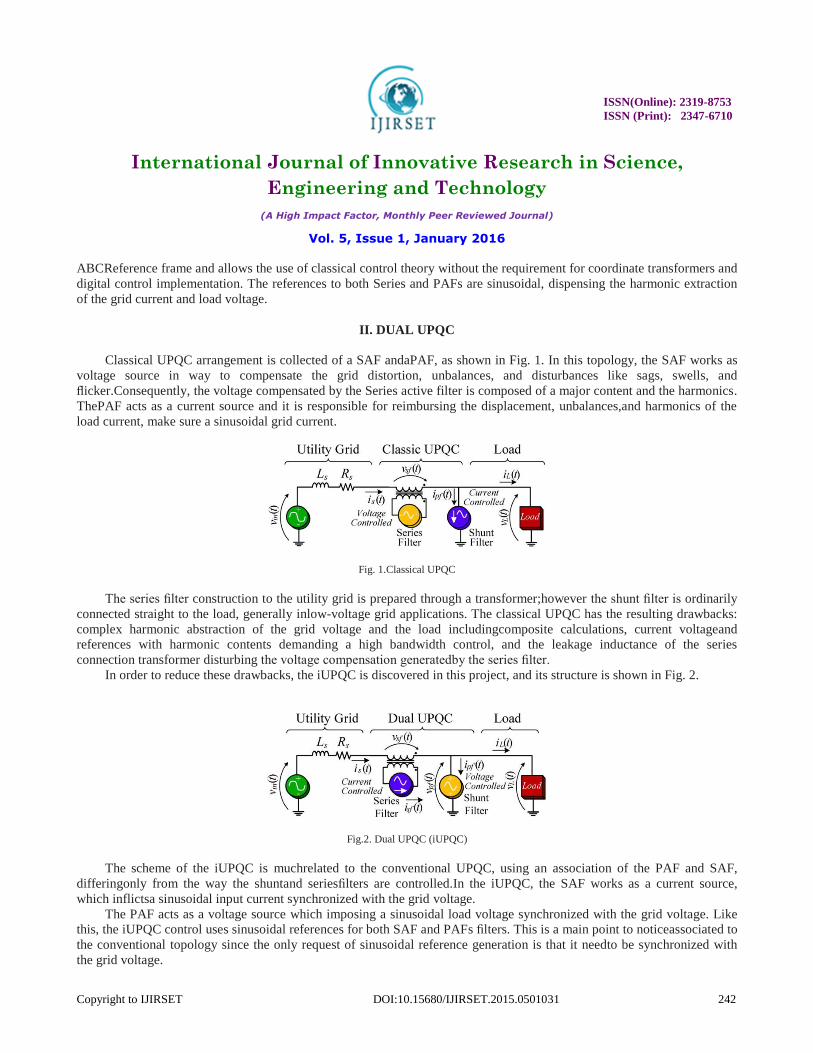
Classical UPQC arrangement is collected of a SAF andaPAF, as shown in Fig. 1. In this topology, the SAF works as
voltage source in way to compensate the grid distortion, unbalances, and disturbances like sags, swells, and
flicker.Consequently, the voltage compensated by the Series active filter is composed of a major content and the harmonics.
ThePAF acts as a current source and it is responsible for reimbursing the displacement, unbalances,and harmonics of the
load current, make sure a sinusoidal grid current.
Fig. 1.Classical UPQC
The series filter construction to the utility grid is prepared through a transformer;however the shunt filter is ordinarily
connected straight to the load, generally inlow-voltage grid applications. The classical UPQC has the resulting drawbacks:
complex harmonic abstraction of the grid voltage and the load includingcomposite calculations, current voltageand
references with harmonic contents demanding a high bandwidth control, and the leakage inductance of the series
connection transformer disturbing the voltage compensation generatedby the series filter.
In order to reduce these drawbacks, the iUPQC is discovered in this project, and its structure is shown in Fig. 2.
Fig.2. Dual UPQC (iUPQC)
The scheme of the iUPQC is muchrelated to the conventional UPQC, using an association of the PAF and SAF,
differingonly from the way the shuntand seriesfilters are controlled.In the iUPQC, the SAF works as a current source,
which inflictsa sinusoidal input current synchronized with the grid voltage.
The PAF acts as a voltage source which imposing a sinusoidal load voltage synchronized with the grid voltage. Like
this, the iUPQC control uses sinusoidal references for both SAF and PAFs filters. This is a main point to noticeassociated to
the conventional topology since the only request of sinusoidal reference generation is that it needto be synchronized with
the grid voltage.
ISSN(Online): 2319-8753
ISSN (Print): 2347-6710
International Journal of Innovative Research in Science,
Engineering and Technology
(A High Impact Factor, Monthly Peer Reviewed Journal)
Vol. 5, Issue 1, January 2016
Copyright to IJIRSET DOI:10.15680/IJIRSET.2015.0501031 243
The series active filter (SAF)worksas high impedance for the current harmonics and secondarilyrecompenses the
harmonics, unbalances, and disturbances of the grid voltage meanwhile the connection transformer voltages are identical to
the variance between the grid voltage and the loadvoltage. Correspondingly, the shunt active filter (PAF) secondarily
compensates the unbalances, displacement, and harmonics of the grid current, providing a low-impedance lane for the
harmonic load current.
III. POWER CIRCUIT
The power circuit of the existing iUPQC is fabricated with pair offour-wire three-phase converters coupled back to back
and their particular output filters, as shown in Fig. 3. The three single-phase transformers are used to connect the SAFto the
utility grid, whereas the PAF is joined directly to the load. Table I displays the specification of the iUPQC. The passive
components are shown in Table II.
Fig.3. Power circuit of iUPQC
TABLE I
DESIGN SPECIFICATIONS OF THE iUPQC
Input line to line voltage Vin= 220V
Output nomial Power Po= 2500VA
DC link voltage Vb= 400V
Utility grid frequency fgrid= 60Hz
Switching frequency of series and PAFs fs = 20kHz
Transformer ratio n = 1
ISSN(Online): 2319-8753
ISSN (Print): 2347-6710
International Journal of Innovative Research in Science,
Engineering and Technology
(A High Impact Factor, Monthly Peer Reviewed Journal)
Vol. 5, Issue 1, January 2016
Copyright to IJIRSET DOI:10.15680/IJIRSET.2015.0501031 244
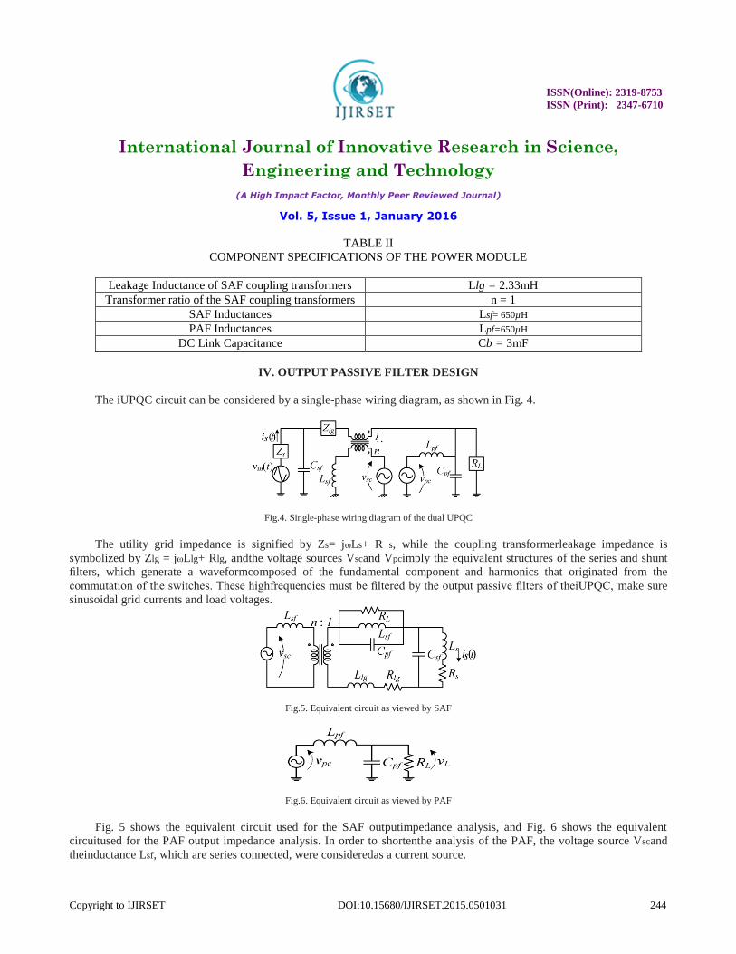
TABLE II
COMPONENT SPECIFICATIONS OF THE POWER MODULE
Leakage Inductance of SAF coupling transformers Llg = 2.33mH
Transformer ratio of the SAF coupling transformers n = 1
SAF Inductances Lsf= 650µH
PAF Inductances Lpf=650µH
DC Link Capacitance Cb = 3mF
IV. OUTPUT PASSIVE FILTER DESIGN
The iUPQC circuit can be considered by a single-phase wiring diagram, as shown in Fig. 4.
Fig.4. Single-phase wiring diagram of the dual UPQC
The utility grid impedance is signified by Zs= jωLs+ R s, while the coupling transformerleakage impedance is
symbolized by Zlg = jωLlg+ Rlg, andthe voltage sources Vscand Vpcimply the equivalent structures of the series and shunt
filters, which generate a waveformcomposed of the fundamental component and harmonics that originated from the
commutation of the switches. These highfrequencies must be filtered by the output passive filters of theiUPQC, make sure
sinusoidal grid currents and load voltages.
Fig.5. Equivalent circuit as viewed by SAF
Fig.6. Equivalent circuit as viewed by PAF
Fig. 5 shows the equivalent circuit used for the SAF outputimpedance analysis, and Fig. 6 shows the equivalent
circuitused for the PAF output impedance analysis. In order to shortenthe analysis of the PAF, the voltage source Vscand
theinductance Lsf, which are series connected, were consideredas a current source.
ISSN(Online): 2319-8753
ISSN (Print): 2347-6710
International Journal of Innovative Research in Science,
Engineering and Technology
(A High Impact Factor, Monthly Peer Reviewed Journal)
Vol. 5, Issue 1, January 2016
Copyright to IJIRSET DOI:10.15680/IJIRSET.2015.0501031 245
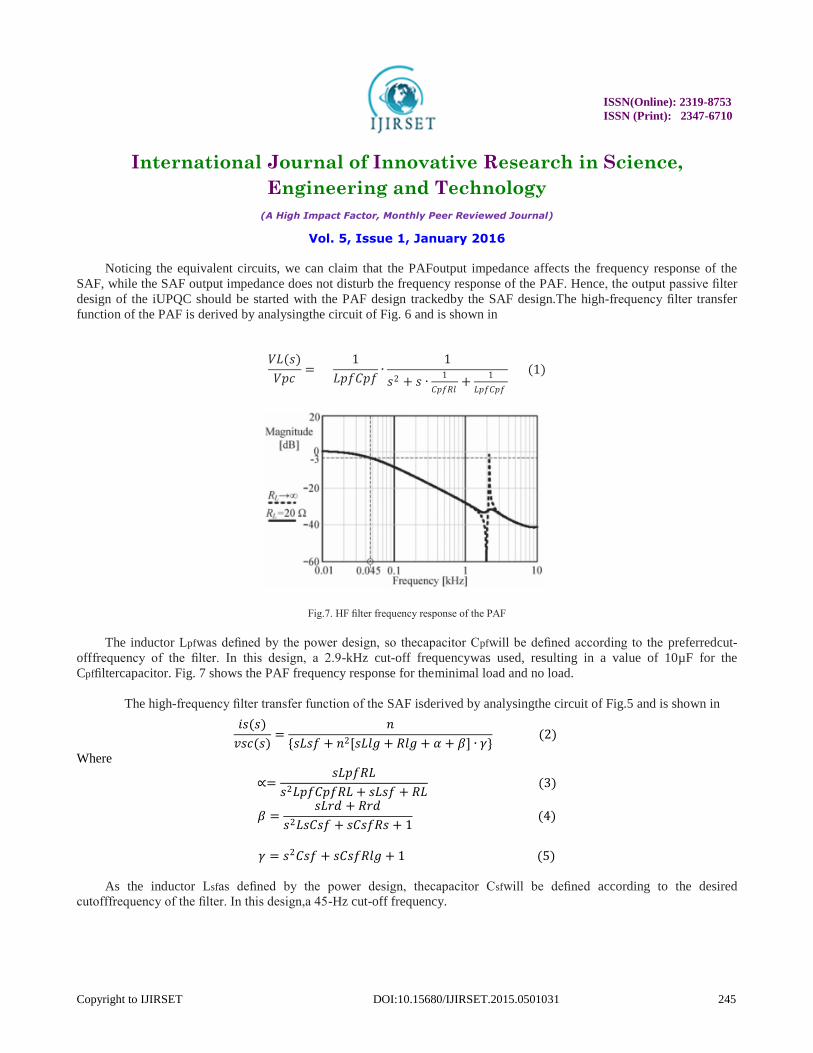
Noticing the equivalent circuits, we can claim that the PAFoutput impedance affects the frequency response of the
SAF, while the SAF output impedance does not disturb the frequency response of the PAF. Hence, the output passive filter
design of the iUPQC should be started with the PAF design trackedby the SAF design.The high-frequency filter transfer
function of the PAF is derived by analysingthe circuit of Fig. 6 and is shown in
𝑉𝐿(𝑠)
𝑉𝑝𝑐=
1
𝐿𝑝𝑓𝐶𝑝𝑓∙
1
𝑠2 + 𝑠 ∙1
𝐶𝑝𝑓𝑅𝑙+
1
𝐿𝑝𝑓𝐶𝑝𝑓
(1)
Fig.7. HF filter frequency response of the PAF
The inductor Lpfwas defined by the power design, so thecapacitor Cpfwill be defined according to the preferredcut-
offfrequency of the filter. In this design, a 2.9-kHz cut-off frequencywas used, resulting in a value of 10µF for the
Cpffiltercapacitor. Fig. 7 shows the PAF frequency response for theminimal load and no load.
The high-frequency filter transfer function of the SAF isderived by analysingthe circuit of Fig.5 and is shown in
𝑖𝑠(𝑠)
𝑣𝑠𝑐(𝑠)=
𝑛
{𝑠𝐿𝑠𝑓 + 𝑛2[𝑠𝐿𝑙𝑔 + 𝑅𝑙𝑔 + 𝛼 + 𝛽] ∙ 𝛾} (2)
Where
∝=𝑠𝐿𝑝𝑓𝑅𝐿
𝑠2𝐿𝑝𝑓𝐶𝑝𝑓𝑅𝐿 + 𝑠𝐿𝑠𝑓 + 𝑅𝐿 (3)
𝛽 =𝑠𝐿𝑟𝑑 + 𝑅𝑟𝑑
𝑠2𝐿𝑠𝐶𝑠𝑓 + 𝑠𝐶𝑠𝑓𝑅𝑠 + 1 (4)
𝛾 = 𝑠2𝐶𝑠𝑓 + 𝑠𝐶𝑠𝑓𝑅𝑙𝑔 + 1 (5)
As the inductor Lsfas defined by the power design, thecapacitor Csfwill be defined according to the desired
cutofffrequency of the filter. In this design,a 45-Hz cut-off frequency.
ISSN(Online): 2319-8753
ISSN (Print): 2347-6710
International Journal of Innovative Research in Science,
Engineering and Technology
(A High Impact Factor, Monthly Peer Reviewed Journal)
Vol. 5, Issue 1, January 2016
Copyright to IJIRSET DOI:10.15680/IJIRSET.2015.0501031 246
Fig.8. HF filter frequency response of the SAF
Fig.8shows the SAF frequency response for nominal load and nowas used, resulting in a value of 1µF for the Csf.As
the inductor Lsfwas defined by the power design, thecapacitor Csfwill be defined according to the preferred cut-
offfrequency of the filter. In this design a 45-Hz cut-off frequency. Fig.8 shows the SAF frequency response for nominal
load and noload. It can be prominent that the filter response has a small cutofffrequency that can moderate the bandwidth of
the SAF, decreasing its efficiency under operation with harmonic contents on thegrid voltage.
This characteristic of low-frequency attenuationis adverse and intrinsic to the structure due to the leakageimpedance
of the coupling transformers.
V. PROPOSED CONTROL SCHEME
The proposed iUPQC control arrangement is an ABC reference structure based control, where the SAF and PAF are
controlled in an independent way.
In the suggested control scheme, the power calculation andharmonic abstraction are not required since the harmonics,
unbalances,disturbances, and displacement would be compensated.
The SAF has a current loop in order to make sure a sinusoidal grid current synchronized with the grid voltage. The
PAF has a voltage loop to ensure a balanced controlled load voltage with small harmonic distortion. The SAF and PAF
control loops areindependent from each other meanwhile they act independently in each active filter. The dc link voltage
control is prepared in the SAF, where the voltage loop describes the amplitude reference for the current loop, in the same
manner of the power factor converter control schemes. The sinusoidal references for both filter controls are generated by a
digital signal processor (DSP),which make sure the grid voltage synchronism using a phase protected loop.
A.SAF Control
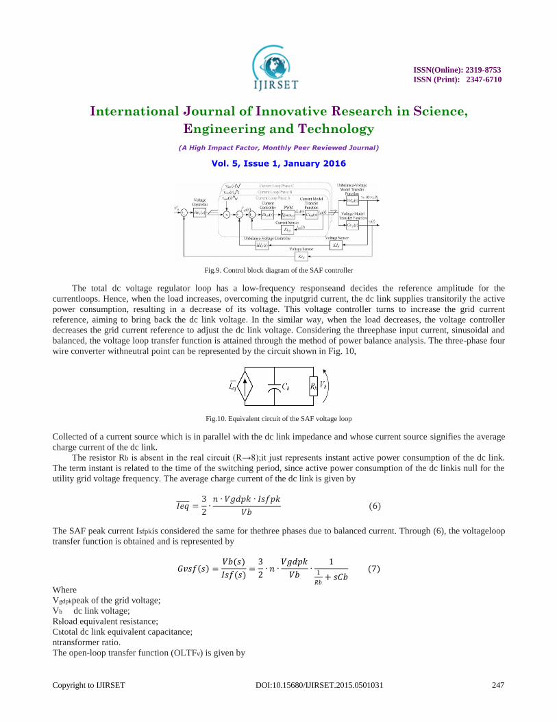
Fig. 9 shows the control block diagrams for the Series active filter (SAF). TheSAF control structure contains of two
voltage loops and three identical grid currentloops. One voltage loop isliable for regulating the total dc link voltage, and the
other is responsible for avoiding the unbalances between the dc link capacitors.The current loops are responsiblefor tracing
the reference of each grid input phase in order tocontrol the grid currents individually.
ISSN(Online): 2319-8753
ISSN (Print): 2347-6710
International Journal of Innovative Research in Science,
Engineering and Technology
(A High Impact Factor, Monthly Peer Reviewed Journal)
Vol. 5, Issue 1, January 2016
Copyright to IJIRSET DOI:10.15680/IJIRSET.2015.0501031 247
Fig.9. Control block diagram of the SAF controller
The total dc voltage regulator loop has a low-frequency responseand decides the reference amplitude for the
currentloops. Hence, when the load increases, overcoming the inputgrid current, the dc link supplies transitorily the active
power consumption, resulting in a decrease of its voltage. This voltage controller turns to increase the grid current
reference, aiming to bring back the dc link voltage. In the similar way, when the load decreases, the voltage controller
decreases the grid current reference to adjust the dc link voltage. Considering the threephase input current, sinusoidal and
balanced, the voltage loop transfer function is attained through the method of power balance analysis. The three-phase four
wire converter withneutral point can be represented by the circuit shown in Fig. 10,
Fig.10. Equivalent circuit of the SAF voltage loop
Collected of a current source which is in parallel with the dc link impedance and whose current source signifies the average
charge current of the dc link.
The resistor Rb is absent in the real circuit (R→8);it just represents instant active power consumption of the dc link.
The term instant is related to the time of the switching period, since active power consumption of the dc linkis null for the
utility grid voltage frequency. The average charge current of the dc link is given by
𝐼𝑒𝑞 =3
2∙𝑛 ∙ 𝑉𝑔𝑑𝑝𝑘 ∙ 𝐼𝑠𝑓𝑝𝑘
𝑉𝑏 (6)
The SAF peak current Isfpkis considered the same for thethree phases due to balanced current. Through (6), the voltageloop
transfer function is obtained and is represented by
𝐺𝑣𝑠𝑓 𝑠 =𝑉𝑏(𝑠)
𝐼𝑠𝑓(𝑠)=
3
2∙ 𝑛 ∙
𝑉𝑔𝑑𝑝𝑘
𝑉𝑏∙
11
𝑅𝑏+ 𝑠𝐶𝑏
(7)
Where
Vgdpkpeak of the grid voltage;
Vb dc link voltage; Rbload equivalent resistance; Cbtotal dc link equivalent capacitance; ntransformer ratio. The open-loop transfer function (OLTFv) is given by
ISSN(Online): 2319-8753
ISSN (Print): 2347-6710
International Journal of Innovative Research in Science,
Engineering and Technology
(A High Impact Factor, Monthly Peer Reviewed Journal)
Vol. 5, Issue 1, January 2016
Copyright to IJIRSET DOI:10.15680/IJIRSET.2015.0501031 248
𝑂𝐿𝑇𝐹𝑣 𝑠 = 𝐺𝑣𝑠𝑓 𝑠 ∙𝐾𝑣𝑠𝑓
𝐾𝑖𝑠𝑓∙ 𝐾𝑚𝑠𝑓 (8)
Where
Kmfsmultiplier gain;
Kvvoltage sensor gain;
Kisfcurrent sensor gain;
The Kmfs gain is attained by considering the gain of the multiplier integrated circuit and the peak of the
synchronizedsinusoidal signal generated by the DSP.
Pointing to regulate the total dc link voltage control, a proportional integral (PI)+pole controller was considered which
ensures a crossover frequency of 4Hz and a phase margin of 45.Frequency response containing the open-loop transfer
function (OLTFv), controllertransfer function (Hvsf), and compensated loop transfer function(OLTFv+ Hvsf).
The unbalanced-voltage control loop also has a low-frequency loop and performances on the dc level of the grid
currentreference in order to keep the voltage balance in dc linkcapacitors. When a voltage unbalance occurs, this loop adds
adc level to the references of the grid currents, aiming to balanceboth CL1and CL2 voltages.
Fig.11. Equivalent circuit of the SAF unbalanced-voltage loop
The unbalanced-voltage loop transfer function is attainedthrough the analysis of the simplified circuit shown in Fig.
11.The four-wire converter permits the single-phase analysis, wheretwo current sources represent the current on the inverter
switches. In Fig. 11, the current Isc(t) represents the currentthrough the neutral point, and d(t) represents the duty cycle.
Through the mesh analysis and by applying Laplace, theunbalanced-voltage loop transfer function is achieved
andgiven by
𝐺𝑑𝑓 𝑠 =𝑉𝑏 + 𝑠 − 𝑉𝑏 − (𝑠)
𝐼𝑠𝑐(𝑠)=
3
2 ∙ 𝑠 ∙ 𝐶𝑏 (9)
The open-loop transfer function (OLTFd) is given by
𝑂𝐿𝑇𝐹𝑑 𝑠 = 𝐺𝑑𝑠𝑓 𝑠 ∙𝐾𝑑𝑠𝑓
𝐾𝑖𝑠𝑓 (10)
Where
Kdsfdifferential voltage sensor gain.
Aiming to abolish the variance dc link voltage, a PI+polecontroller was designed, which ensures a crossover
frequencyof 0.5 Hz and a phase margin of 50.Frequency response includingthe open-loop transfer function (OLTFd),
controller transferfunction(Hdsf), and compensated loop transfer function(OLTFd+Hdsf).
ISSN(Online): 2319-8753
ISSN (Print): 2347-6710
International Journal of Innovative Research in Science,
Engineering and Technology
(A High Impact Factor, Monthly Peer Reviewed Journal)
Vol. 5, Issue 1, January 2016
Copyright to IJIRSET DOI:10.15680/IJIRSET.2015.0501031 249
Fig.12. Single-phase equivalent circuit of SAF
The current control scheme contains of three equal current loops, except for the 120phase displacements from
thereferences of each other. The current loops have a fast response to track the sinusoidal references, agreeing the
decoupling analysis in relation to the voltage loop. The current loop transfer function is acquired through the analysis of the
single-phase equivalent circuit shown in Fig. 12.
The voltage source represents the voltage on the coupling transformer. The dynamic model is obtained through the
circuit analysis using average values associated to the switching period. Under these conditions, the voltages Vs(t) and
VL(t) are constants. Through small signal analysis and by using Laplace, thecurrent loop transfer function is given by
𝐺𝑖𝑓𝑠 𝑠 =𝐼𝑠𝑐(𝑠)
𝐷(𝑠)=
𝑉𝑏
𝑠𝐴1 + 𝑛2 ∙ (𝑅𝑠 + 𝑅𝑙𝑔) (11)
Where
𝐴1 = 𝑛2 ∙ 𝐿𝑠 + 𝐿𝑙𝑔 + 𝐿𝑠𝑓 (12)
and
Lsseries grid inductance;
RsSeries grid resistance;
Llgleakage inductance of the coupling transformer;
Rlgseries resistance of the coupling transformer.
The open-loop transfer function (OLTFi) is given by
The Kpwmsfgain is equal to the inverse peak value of thetriangular carrier.
Aiming to track the current reference, a PI+pole controller was designed, which ensures a crossover frequency of 5
kHz and a phase margin of 70.Frequency responsehaving the open-loop transfer function (OLTFi), controller transfer
function (Hisf), and compensated loop transfer function (OLTFi+ Hisf).
ISSN(Online): 2319-8753
ISSN (Print): 2347-6710
International Journal of Innovative Research in Science,
Engineering and Technology
(A High Impact Factor, Monthly Peer Reviewed Journal)
Vol. 5, Issue 1, January 2016
Copyright to IJIRSET DOI:10.15680/IJIRSET.2015.0501031 250
B. PAF Control
Fig.13. Control block diagram of the PAF voltage loop
Fig. 13 shows the control block diagram of the Parallel Active Filter (PAF) controller.The PAF control scheme is
designed by three identical load voltage feedback loops, excluding for the 1200 phase displacements from the references of
each other. The voltage loops are liable for tracing the sinusoidal voltage reference for each load output phase in order to
control the load voltages individually.
Fig.14. Single-phase equivalent circuit of PAF
The voltage loop transfer function is obtained through the analysis of the single-phase equivalent circuit shown in Fig.
14. The dynamic model is attained through the circuit analysis using average values related to the switching period.
Through small signal analysis and by using Laplace,the voltage loop transfer function is given by
𝐺𝑣𝑝𝑓 𝑠 =𝑉𝑏
𝐿𝑝𝑓𝐶𝑝𝑓∙
1
𝑠2 + 𝑠 1
𝐶𝑝𝑓𝑅𝐿 +
1
𝐿𝑝𝑓𝐶𝑝𝑓
(14)
Where Gvpf(s)=VL(s)/D(s). The open-loop transfer function (OLTFvpf) is given by
𝑂𝐿𝑇𝐹𝑣 𝑠 = 𝑔𝑣𝑝𝑓 𝑠 ∙ 𝐾𝑝𝑤𝑚𝑝𝑓𝐾𝑣𝑝𝑓 (15)
Where
Kpwmpfshunt filter PWM modulator gain.
ISSN(Online): 2319-8753
ISSN (Print): 2347-6710
International Journal of Innovative Research in Science,
Engineering and Technology
(A High Impact Factor, Monthly Peer Reviewed Journal)
Vol. 5, Issue 1, January 2016
Copyright to IJIRSET DOI:10.15680/IJIRSET.2015.0501031 251
Aiming to trace the voltage reference, a proportional integral derivative (PID)+additional pole controller was
designed, which make sure a crossover frequency of 4 kHz and a phase margin of 35. Frequency response containing the
open-loop transfer function (OLTFvpf), controller transfer function (Hvpf), and compensated loop transfer function
(OLTFvpf+ Hvpf).
In stable state, assuming a sinusoidal and balanced utility grid voltage and disregarding the dual UPQC losses, the
apparent power of SAF Ssf and PAF Spf regularized in relation to the apparent power of the load are given by (16) and (17).
𝑆𝑠𝑓
𝑆𝐿 =
cos𝜑1 ∙ (1 −𝑉𝐿
𝑉𝑠)2
1 + 𝑇𝐷𝐻𝑖2 (16)
𝑆𝑝𝑓
𝑆𝐿 =
𝑐𝑜𝑠2𝜑1 ∙𝑉𝐿
𝑉𝑆∙
𝑉𝐿
𝑉𝑆− 2
1 + 𝑇𝐷𝐻𝑖2+ 1 (17)
Where cos(ϕ1) is the displacement factor and THDi is the total harmonic distortion of the output current.
These equations are attained through the analysis of the complex power of SAFS sf and PAF S pf
𝑆𝑠𝑓 = 𝑉𝑠 − 𝑉𝐿 ∙ 𝐼∗𝑠
18
𝑆𝑝𝑓 = 𝑆𝐿 − 𝑉𝑙 ∙ 𝐼∗𝑠 (19)
Increasing THDi and decreasing cos(ϕ1) will decrease the ratio of |Ssf/SL| and will increase the ratio of |Spf/SL|.
This exploration indications that it is possible to design a SAF with power capacity lower than the minimal load
power. By varying the transformers ratio, it is possible to use power switches with minor current capacity. On the other
hand, PAF is constantly designed for nominal load power from the time when it has to process the total load reactive
power.
VI. EXPERIMENTAL RESULTS
Experimental results for the proposed iUPQC. The passive filters were designed according to the specifications of
Table I.
The Precharge system and the Precharge structure are an important and not trivial design step of the iUPQC due to the
power flow characteristics of the system. During the start-up, the voltage supplied to the load cannot be distorted, and the
iUPQC coupling in the circuit will not affect the load. The precharge method developed permits the start-up of the iUPQC
without requirement of load power disconnection. The used precharge sequence is shown in Fig. 15. The precharge circuit
has three contactors, namely, Ks,Kp1,andKp2, and one in-rush resistorRpc. The switches Sw1and Sw2are used symbolically
to showthe switching turn-on time. The Kp1and Kp2contactors are initially opened, while the Kscontactor is initially closed,
and the switching of both active filters is primarily disabled.
The precharge sequence starts when the contactor Kp1 is turned on, providing the charge of the dc link capacitors
through antiparallel diodes present in the PAF power circuit. After 340 ms, the switching of the SAF Sw1is enabled, causing
avoltage unbalance on the dc link during a short period of timedue to the stabilization time of the SAF unbalanced-voltage
control loop. After 1 s, the Ks
Contactor is turned off, allowing the increase of the dc link voltage by SAF operation. After 10 ms, the switching of
the PAF Sw2is enabled, starting theregulation of the load voltage. After 100 ms, the Kp2is turned on, finishing the precharge
ISSN(Online): 2319-8753
ISSN (Print): 2347-6710
International Journal of Innovative Research in Science,
Engineering and Technology
(A High Impact Factor, Monthly Peer Reviewed Journal)
Vol. 5, Issue 1, January 2016
Copyright to IJIRSET DOI:10.15680/IJIRSET.2015.0501031 252
sequence. In order to match a harmonic distorted load current, a three phase rectifier with capacitive filter and two single-
phase rectifiers with RL load connected to phases A and B, correspondingly, was used.
Fig.15. Precharge sequence of the iUPQC
In order to match a distorted grid voltage and to evaluate the harmonic compensation of the grid voltage, a FCATH
450-38-50 programmable ac power source manufactured by SUPPLIER Inc. was used. The power source supplies a
threephase voltage source with 20% of the third harmonic in phaseA, 10% of the fifth harmonic in phase B, and 10% of the
seventh harmonic in phase C.
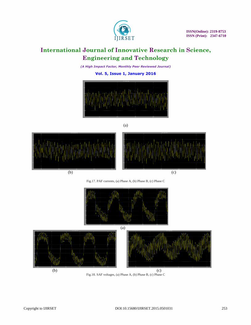
Fig. 17 shows the currents through the PAF. The PAF indirectly supplies the load harmonic currents because the SAF
only drains the fundamental current component from the source.
In a similar manner, Fig. 18 shows the voltages synthesized by the SAF. The SAF indirectly processes the harmonic
grid voltages because the PAF imposes a synchronized sinusoidal voltage on the load.
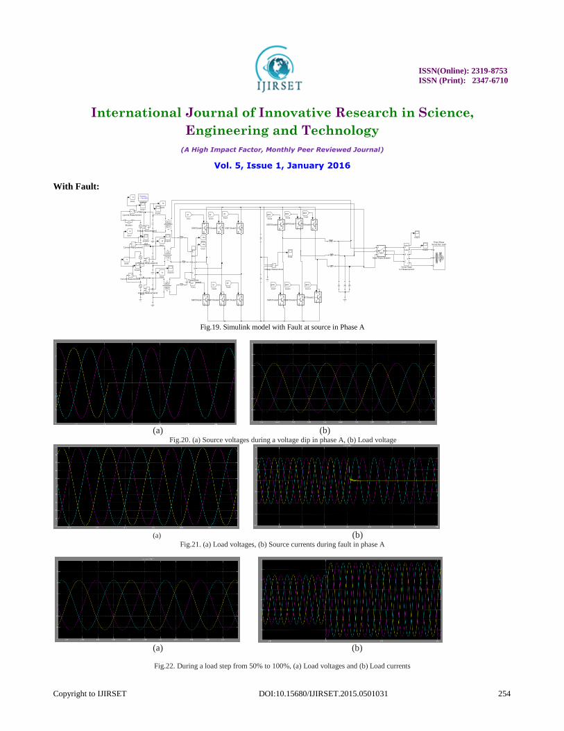
In order to verify the dynamic response of the iUPQC, Fig. 20 shows the source and load voltages during a voltage
interruption in phase A. Fig. 21 shows the source currents during a fault in phase A. It is possible to see that the source
currents in the other phases have the amplitudes increased in order to keep the nominal power of the load.
Fig. 22 shows the load voltages and the load currentsduring a load step from 50% to 100%. The load voltages andthe
load currents are shown in Fig. 23 during a load step from 100% to 50%.
Without Fault:
Fig.16. Simulink model without Fault
Discrete,Ts = 5e-005 s.
powergui
v+-
Voltage Measurement3
v+-
Voltage Measurement2
v+-
Voltage Measurement1
v+-
Voltage Measurement
IabcA
B
C
a
b
c
VabcA
B
C
a
b
c
Three-PhaseV-I Measurement2
A
B
C
a
b
c
Three-PhaseV-I Measurement1
Vabc
Iabc
A
B
C
a
b
c
Three-PhaseV-I Measurement
A
B
C
Three-PhaseSeries RLC Load
Scope9
Scope8
Scope7
Scope4
Scope3
Scope2
Scope18
Scope17
Scope16
Scope15
Scope14 Scope13
Scope12
Scope11
Scope10
Scope1
Scope
SAF CONTROLLER PAF CONTROLLER
12
12
12
gm
CE
IGBT/Diode9
gm
CE
IGBT/Diode8
gm
CE
IGBT/Diode7
gm
CE
IGBT/Diode6
gm
CE
IGBT/Diode5
gm
CE
IGBT/Diode4
gm
CE
IGBT/Diode3
gm
CE
IGBT/Diode2
gm
CE
IGBT/Diode11
gm
CE
IGBT/Diode10
gm
CE
IGBT/Diode1
gm
CE
IGBT/Diode
ipfa
Goto5
vsfa
Goto4
vc
Goto3
vb
Goto2
va
Goto1
[g52]
From9
[g32]
From8
[g22]
From7
[g12]
From6
g6
From5
g5
From4
g4
From3
g2
From2
ipfa
From13
vsfa
From12
[g62]
From11
[g42]
From10
g3
From1
g1
From
i+
-
Current Measurement2
i+
-
Current Measurement1
i+
-
Current Measurement
ISSN(Online): 2319-8753
ISSN (Print): 2347-6710
International Journal of Innovative Research in Science,
Engineering and Technology
(A High Impact Factor, Monthly Peer Reviewed Journal)
Vol. 5, Issue 1, January 2016
Copyright to IJIRSET DOI:10.15680/IJIRSET.2015.0501031 253
(a)
(b) (c)
Fig.17. PAF currents, (a) Phase A, (b) Phase B, (c) Phase C
(a)
(b) (c)
Fig.18. SAF voltages, (a) Phase A, (b) Phase B, (c) Phase C
ISSN(Online): 2319-8753
ISSN (Print): 2347-6710
International Journal of Innovative Research in Science,
Engineering and Technology
(A High Impact Factor, Monthly Peer Reviewed Journal)
Vol. 5, Issue 1, January 2016
Copyright to IJIRSET DOI:10.15680/IJIRSET.2015.0501031 254
With Fault:
Fig.19. Simulink model with Fault at source in Phase A
(a) (b)
Fig.20. (a) Source voltages during a voltage dip in phase A, (b) Load voltage
(a) (b)
Fig.21. (a) Load voltages, (b) Source currents during fault in phase A
(a) (b)
Fig.22. During a load step from 50% to 100%, (a) Load voltages and (b) Load currents
Discrete,Ts = 5e-005 s.
powergui
v+-
Voltage Measurement3
v+-
Voltage Measurement2
v+-
Voltage Measurement1
v+-
Voltage Measurement
A
B
C
a
b
c
Three-Phase Breaker
Vabc
Iabc
A
B
C
a
b
c
Three-PhaseV-I Measurement2
Vabc
Iabc
A
B
C
a
b
c
Three-PhaseV-I Measurement
A
B
C
Three-PhaseSeries RLC Load
Scope5
Scope4
Scope3
Scope2
Scope16
Scope15
Scope14 Scope13
Scope10
Scope1
Scope
SAF CONTROLLER PAF CONTROLLER
12
12
12
gm
CE
IGBT/Diode9
gm
CE
IGBT/Diode8
gm
CE
IGBT/Diode7
gm
CE
IGBT/Diode6
gm
CE
IGBT/Diode5
gm
CE
IGBT/Diode4
gm
CE
IGBT/Diode3
gm
CE
IGBT/Diode2
gm
CE
IGBT/Diode11g
m
CE
IGBT/Diode10
gm
CE
IGBT/Diode1
gm
CE
IGBT/Diode
ic
Goto8
ib
Goto7
ia
Goto6
isfa
Goto5
vsfa
Goto4
vc
Goto3
vb
Goto2
va
Goto1
[g52]
From9
[g32]
From8
[g22]
From7
[g12]
From6
g6
From5
g5
From4
g4
From3
g2
From2
ic
From17
ib
From16vc
From15
vb
From14
va
From13ia
From12
[g62]
From11
[g42]
From10
g3
From1
g1
From
i+
-
Current Measurement2
i+
-
Current Measurement1
i+
-
Current Measurement
Breaker
ISSN(Online): 2319-8753
ISSN (Print): 2347-6710
International Journal of Innovative Research in Science,
Engineering and Technology
(A High Impact Factor, Monthly Peer Reviewed Journal)
Vol. 5, Issue 1, January 2016
Copyright to IJIRSET DOI:10.15680/IJIRSET.2015.0501031 255
(a) (b)
Fig.23. During a load step from 100% to 50%, (a) Load voltage and (b) Load currents
VII.CONCLUSION
The results acquired through the iUPQC confirms that the recommendedABC reference mount control works very fine
and thatit was capable to compensate the nonlinear load currents and similarlyensure the sinusoidal voltage for the load in
all three phases. The control too had excessive performance during the load steps and voltage disorders at the source.
The main benefits of this proposed control in relativeto the other proposed systems were the consumption of
sinusoidalreferences for both series and shunt active filtercontrols without the need for complex calculations or
synchronizetransformations. The iUPQC references do not require harmonic contents, and the only constraint is the synchronism with the grid
voltage. Additional positive aspect of the iUPQC in low-voltage applications(Distribution system network) is the non-
interference of the leakage impedance voltage of the series active filter (SAF) connection transformer in the load voltage
compensation since the load voltage is directly controlled by the PAF. On the other hand, the leakage impedance affects in
the current loop bandwidth, reducing its frequency response below distorted grid voltages.
The results confirm the proposed iUPQC control arrangement, evidencing that the power quality can be expressively
better with a simple control method which uses only synchronized sinusoidal references.
REFERENCES
[1] M. Aredes, K. Heumann, and E. Watanabe, ―An universal active powerline conditioner,‖ IEEE Trans. Power Del., vol. 13, no. 2, pp. 545–551,Apr. 1998.
[2] H. Fujita and H. Akagi, ―The unified power quality conditioner: The integration of series and shunt-active filters,‖ IEEE Trans. Power Electron., vol.
13, no. 2, pp. 315–322, Mar. 1998.
[3] B. Han, B. Bae, S. Baek, and G. Jang, ―New configuration of UPQC formedium-voltage application,‖ IEEE Trans. Power Del., vol. 21, no. 3,pp. 1438–
1444, Jul. 2006.
[4] S.Chakraborty, M.Weiss, and M.Simoes, ―Distributed intelligent energymanagement system for a single-phase high-frequency ac microgrid,‖IEEE Trans. Ind. Electron., vol. 54, no. 1, pp. 97–109, Feb. 2007.
[5] M. Forghani and S. Afsharnia, ―Online wavelet transform-based control strategy for UPQC control system,‖ IEEE Trans. Power Del., vol. 22, no. 1,
pp. 481–491, Jan. 2007. [6] A. Jindal, A. Ghosh, and A. Joshi, ―Interline unified power quality conditioner,‖ IEEE Trans. Power Del., vol. 22, no. 1, pp. 364–372, Jan. 2007.
[7] Y. Kolhatkar and S. Das, ―Experimental investigation of a single-phase UPQC with minimum VA loading,‖ IEEE Trans. Power Del., vol. 22, no. 1,
pp. 373–380, Jan. 2007. [8] M. Basu, S. Das, and G. Dubey, ―Investigation on the performance of UPQC-Q for voltage sag mitigation and power quality improvement at critical
load point,‖ IET Gen. Transmiss. Distrib., vol. 2, no. 3, pp. 414– 423, May 2008.
[9] V. Khadkikar and A. Chandra, ―A new control philosophy for a unified power quality conditioner (UPQC) to coordinate load-reactive power demand between shunt and series inverters,‖ IEEE Trans. Power Del., vol. 23, no. 4, pp. 2522–2534, Oct. 2008.
[10] M. Aredes and R. Fernandes, ―A dual topology of unified power quality conditioner: The iUPQC,‖ in Proc. 13th Eur. Conf. Power Electron. Appl.,
Sep. 2009, pp. 1–10.
ISSN(Online): 2319-8753
ISSN (Print): 2347-6710
International Journal of Innovative Research in Science,
Engineering and Technology
(A High Impact Factor, Monthly Peer Reviewed Journal)
Vol. 5, Issue 1, January 2016
Copyright to IJIRSET DOI:10.15680/IJIRSET.2015.0501031 256
[11] M. Brenna, R. Faranda, and E. Tironi, ―A new proposal for power quality and custom power improvement: OPEN UPQC,‖ IEEE Trans. Power Del.,
vol. 24, no. 4, pp. 2107–2116, Oct. 2009.
[12] S. Chakraborty and M. Simoes, ―Experimental evaluation of active filtering in a single-phase high-frequency ac microgrid,‖ IEEE Trans. EnergyConvers., vol. 24, no. 3, pp. 673–682, Sep. 2009.
[13] V. Khadkikar and A. Chandra, ―A novel structure for three-phase four-wire distribution system utilizing unified power quality conditioner (UPQC),‖
[14] K. H. Kwan, Y. C. Chu, and P. L. So, ―Model-based H
8unified power quality conditioner,‖ IEEE Trans. Ind. Electron., vol. 56,no. 7, pp. 2493–2504, Jul. 2009.
[15] J. Munoz, J. Espinoza, L. Moran, and C. Baier, ―Design of a modular UPQC configuration integrating a components economic analysis,‖ IEEE Trans. Power Del., vol. 24, no. 4, pp. 1763–1772, Oct. 2009.
[16] I. Axente, J. Ganesh, M. Basu, M. Conlon, and K. Gaughan, ―A 12-kVA DSP-controlled laboratory prototype UPQC capable of mitigating unbalance
in source voltage and load current,‖ IEEE Trans. Power Electron., vol. 25, no. 6, pp. 1471–1479, Jun. 2010. [17] I. Axente, M. Basu, M. Conlon, and K. Gaughan, ―Protection of unified power quality conditioner against the load side short circuits,‖ IET
PowerElectron., vol. 3, no. 4, pp. 542–551, Jul. 2010.
[18] S. Karanki, M. Mishra, and B. Kumar, ―Particle swarm optimizationbased feedback controller for unified power-quality conditioner,‖ IEEETrans. Power Del., vol. 25, no. 4, pp. 2814–2824, Oct. 2010.
[19] W. C. Lee, D. M. Lee, and T.-K. Lee, ―New control scheme for a unified power-quality compensator-Q with minimum active power injection,‖ IEEE
Trans. Power Del., vol. 25, no. 2, pp. 1068–1076, Apr. 2010. [20] B. Franca and M. Aredes, ―Comparisons between the UPQC and its dual topology (iUPQC) in dynamic response and steady-state,‖ in Proc. 37thIEEE
IECON/IECON, Nov. 2011, pp. 1232–1237.
[21] M. Kesler and E. Ozdemir, ―Synchronous-reference-frame-based control method for UPQC under unbalanced and distorted load conditions,‖ IEEETrans. Ind. Electron., vol. 58, no. 9, pp. 3967–3975, Sep. 2011.
[22] V. Khadkikar and A. Chandra, ―UPQC-S: A novel concept of simultaneous voltage sag/swell and load reactive power compensations utilizing series
inverter of UPQC,‖ IEEE Trans. Power Electron., vol. 26, no. 9, pp. 2414–2425, Sep. 2011.
[23] V. Khadkikar, A. Chandra, A. Barry, and T. Nguyen, ―Power quality enhancement utilising single-phase unified power quality conditioner: Digital
signal processor-based experimental validation,‖ IET Power Electron., vol. 4, no. 3, pp. 323–331, Mar. 2011.
[24] V. Kinhal, P. Agarwal, and H. Gupta, ―Performance investigation of neural-network-based unified power-quality conditioner,‖ IEEE Trans.Power Del., vol. 26, no. 1, pp. 431–437, Jan. 2011.
[25] A. Leon, S. Amodeo, J. Solsona, and M. Valla, ―Non-linear optimal controller for unified power quality conditioners,‖ IET Power Electron., vol. 4,
no. 4, pp. 435–446, Apr. 2011.
BIOGRAPHY
N.Manjunath Naidu received B.Tech degree Form (Electrical & Electronics Engineering) in Sri
Venkateswara College of engineering and technology, Chittoor (JNTUA) in 2013. Pursuing M.Tech
(power Electronics) from KEC, Kuppam (JNTUA), and his research areas Include Power Electronics,
UPQC, active filters in Transmission system.
S.Zabiullah M.Tech. Working as Assistant Professor, he was awarded M.Tech(Power Electronics and
Electrical drives) from SriVenkateswara College of Engineering & Technology in Chittoor (JNTUA) in
2011, he was awarded B.Tech from (JNTUA) in 2009. He has 5 years of teaching experience. His area
of interest is Power Electronics &its applications.