Abstract: Integer addition is one of the most importantoperations in digital computer systems because theperformance of processors is significantly influenced by thespeed of their adders. This paper describe the design of a 16-bitparallel self-timed adder (PASTA) &Parallel self-timedsubtractor (PASTS) using VHDL.PASTA design usesmultiplexers along with half adders. PASTS design usesmultiplexers along with half subtractor. Subtraction wasimplemented by PASTS &2’s complement addition usingPASTA. It is based on a recursive formulation for performingmultibit binary addition. The operation is parallel for thosebits that do not need any carry chain propagation. Thesimulation results show the proposed model attains with lesstime and with less complexity.
Index Terms- asynchronous circuits, binary adders, binarysubtractor
I. INTRODUCTIONThe most important operation of processor that can
perform is binary addition. The operation is based on therecursive formulation for performing multibit binary addition.The binary subtraction is another arithmetic operation.The serial adder has slower, uses shift registers, requires onefull adder circuit, Time required for addition depends onnumber of bits and it is sequential circuit. But the paralleladder is Faster, It uses registers with parallel load capacity,No. of full adder circuit is equal to No. of bits in binary adderand time required does not depend on the number of bits.Here half adders are used instead of full adder .Here theoperation is parallel for those bits so that no need any carrychain propagation.
In cellular phones, PDA and other high performance,the clockless chip processor approach must be needed.Clockless processors also called asynchronous or self -timed.In self timed system, that doesn’t use the oscillating crystalthat serves as the regularly “ticking” clock [2]. So the clockless chip will run faster than clock chip in order to avoid theneed of clock tick. Also in clockless chip, the majoradvantage that have of low electromagnetic interference.
Asynchronous circuits do not assume anyquantization of time. In absence of clocks, the logic flow in
asynchronous circuit is controlled byrequest –acknowledgement handshaking protocol. Buthandshaking block for small elements, such as bit adders andbit subtractions are expensive. So these managed using dualrail carry propagation in adders and borrow propagation insubtractor.
The system presents an asynchronous parallel selftimed subtractor (PASTS) proposed using the PASTA [1].The algorithm of PASTA is mainly depends on cellularautomata [4]. This system also implements 2’s complementaddition for subtraction. The design of PASTA&PASTS isregular and uses half adders and half subtractor along withmultiplexers requiring minimal inter connectionsrespectively.
II.LITERATURE SURVEYAddition is a fundamental operation for any digital
system, digital signal processing or control system. A fast andaccurate operation of a digital system is greatly influenced bythe performance of the resident adders. Adders are also veryimportant component in digital systems because of theirextensive use in other basic digital operations such assubtraction, multiplication and division.
A. Ripple Carry AdderThe ripple carry adder is constructed by cascading
full adders (FA) blocks in series. One full adder isresponsible for the addition of two binary digits at any stageof the ripple carry. The carryout of one stage is fed directly tothe carry-in of the next stage. A number of full adders may beadded to the ripple carry adder or ripple carry adders ofdifferent sizes may be cascaded in order to accommodatebinary vector strings of larger sizes. For an n-bit paralleladder, it requires n computational elements (FA). One of themost serious drawbacks of this adder is that the delayincreases linearly with the bit length. As mentioned before,each full adder has to wait for the carry out of the previousstage to output steady-state result. Therefore even if the adderhas a value at its output terminal, it has to wait for thepropagation of the carry before the output reaches a correctvalue
A PARALLEL SELF-TIMED ADDER(PASTA) AND SUBTRACTOR (PASTS)
USING VHDL
1Jismy Theresa,PG Scholar in VLSI Design,
2Manju V.MAssistant Professor, ECE Department,
3Veena KAssistant Professor, ECE Department,
IES college of Engineering, Thrissur, Kerala
ISSN: 2278 – 909XInternational Journal of Advanced Research in Electronics and Communication Engineering (IJARECE)
B. Carry Look-Ahead AdderIn the ripple-carry adder, its limiting factor is the
time it takes to propagate the carry. The carry look-aheadadder [3] solves this problem by calculating the carry signalsin advance, based on the input signals. The result is a reducedcarry propagation time. The Propagate P and generate G in afull-adder, is given as:Pi = Carry propagate
Carry generate
Both propagate and generate signals depend only on the inputbits and thus will be valid after one gate delay. The newexpressions for the output sum and the carryout are given by:
These equations show that a carry signal will be generated intwo cases:1) If both bits and are 1
2) If either or is 1 and the carry-in is 1.
Let's apply these equations for a 4-bit adder:
These expressions show that and do not depend on
its previous carry-in. Therefore does not need to wait for
to propagate. As soon as is computed can reach
steady state. The same is also true for and .The general
expression is
C Asynchronous Adders
C.1 Carry-Completion Sensing AddersA Carry-Completion Sensing Adder (CCSA) [3] may be
regarded as an asynchronous version of an RCA. Instead ofusing clock pulses to synchronize adder operation, a CCSAuses some extra circuitry to implement the start andcompletion signals.. The CCSA scheme computes the inthe following way:
Where
The primary inputs, Ai and Bi, are single rail. The carrybits are encoded by using two separate signals (dual-railsignaling): means that no carry emerges from theith one-bit adder and means that a carry emergesfrom the ith one-bit adder. The completion or acknowledgesignal ( ) for each stage is turned on by the arrival ofeither .This is most economically detected by anOR-gate. If desired, an AND-gate can be added to flag theerror condition . Once all the stages havecomputed their carries, the addition is completed. An n-inputAND gate may be used to signal the completion(i.e, . The enable signal is used to startthe computation and to ensure that no false completion signalwill be generated. When enable = 0, all (i = 1…n)signals are set to zero. The completion signal, finish, must bezero, too. Thus, no false completion can be asserted. After allthe input data have arrived at the input ports of the CCSA, theenable signal is turned on to start the addition operation.Upon the completion of the addition, the finish signal isturned on.
III.DESIGN OF PASTA&PASTSAdders have a special significance in VLSI designs
and it is used in computer and many other processors toperform the arithmetic functions. The adder first accepts twoinput operands to perform half additions for each bit.Subsequently, it iterates using earlier generated carry andsum to perform half additions repeatedly until all carry bitsare consumed and settled at zero level [1].
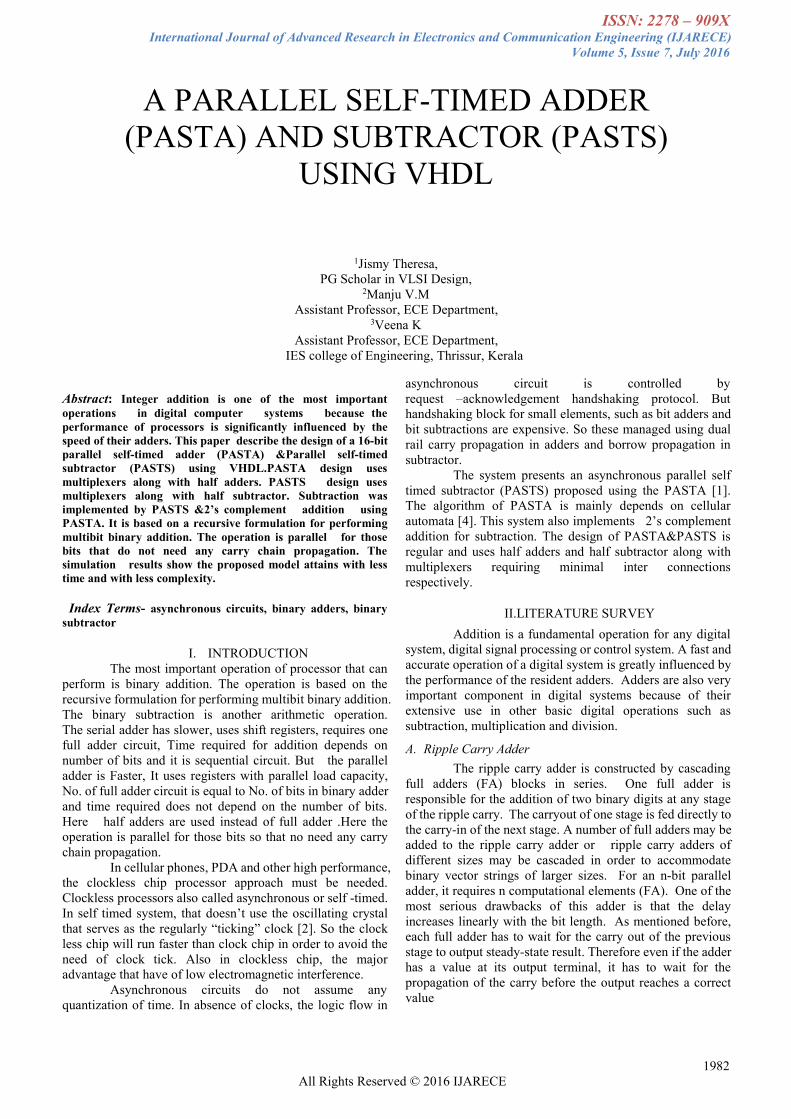
A .ARCHITECTURE OF PASTAThe system mainly includes mux, half adder, and
completion detection unit as shown in fig2. The system dealsVHDL implementation of two 16-bit number additions usingexisting technique PASTA [1]. Here completion detectionunit directly checking all carry bits is zero or not. If all carrybits are zero the output can be displayed.
Fig 1: state diagram [1] (a) initial phase(b) iterative phase
ISSN: 2278 – 909XInternational Journal of Advanced Research in Electronics and Communication Engineering (IJARECE)
The selection input for two input multiplexerscorresponds to the Req-handshake signal and will be a single0 to 1 transition denoted by Sel. It will initially select theactual operands during Sel=0and will switch tofeedback/carry paths for subsequent iterations using Sel=1.The feedback path from the HAs enable the multipleiterations to continue until the completion when all carrysignals will assume zero values. The main working principlerelated with quantum cellur automata[4]
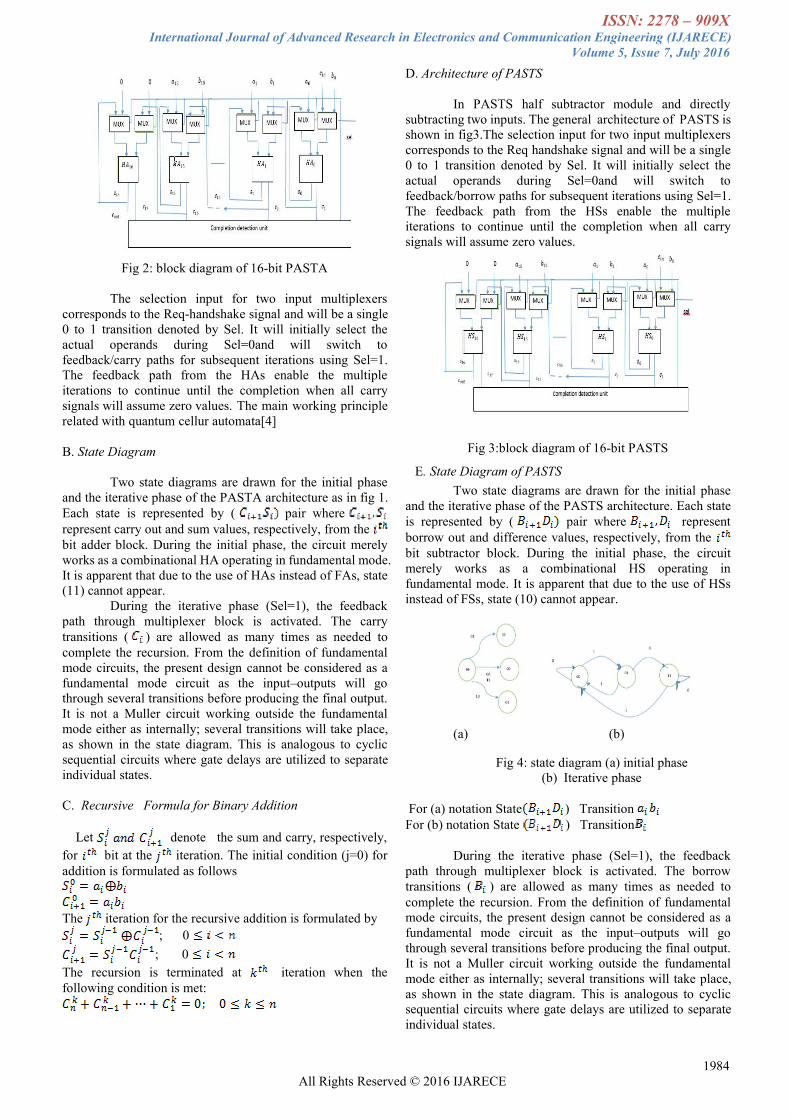
B. State Diagram
Two state diagrams are drawn for the initial phaseand the iterative phase of the PASTA architecture as in fig 1.Each state is represented by ( pair whererepresent carry out and sum values, respectively, from thebit adder block. During the initial phase, the circuit merelyworks as a combinational HA operating in fundamental mode.It is apparent that due to the use of HAs instead of FAs, state(11) cannot appear.
During the iterative phase (Sel=1), the feedbackpath through multiplexer block is activated. The carrytransitions ( ) are allowed as many times as needed tocomplete the recursion. From the definition of fundamentalmode circuits, the present design cannot be considered as afundamental mode circuit as the input–outputs will gothrough several transitions before producing the final output.It is not a Muller circuit working outside the fundamentalmode either as internally; several transitions will take place,as shown in the state diagram. This is analogous to cyclicsequential circuits where gate delays are utilized to separateindividual states.
C. Recursive Formula for Binary Addition
Let denote the sum and carry, respectively,for bit at the iteration. The initial condition (j=0) foraddition is formulated as follows
The iteration for the recursive addition is formulated by; 0; 0
The recursion is terminated at iteration when thefollowing condition is met:
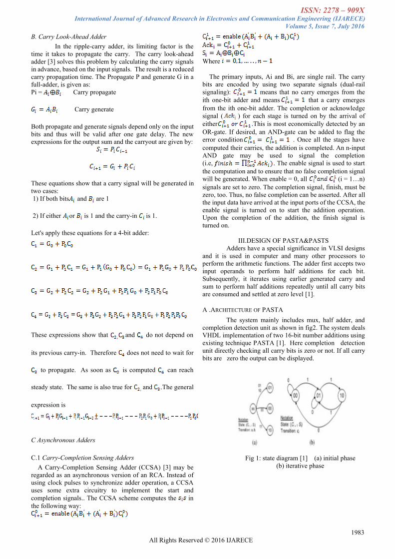
D. Architecture of PASTS
In PASTS half subtractor module and directlysubtracting two inputs. The general architecture of PASTS isshown in fig3.The selection input for two input multiplexerscorresponds to the Req handshake signal and will be a single0 to 1 transition denoted by Sel. It will initially select theactual operands during Sel=0and will switch tofeedback/borrow paths for subsequent iterations using Sel=1.The feedback path from the HSs enable the multipleiterations to continue until the completion when all carrysignals will assume zero values.
Fig 3:block diagram of 16-bit PASTS
E. State Diagram of PASTSTwo state diagrams are drawn for the initial phase
and the iterative phase of the PASTS architecture. Each stateis represented by ( pair where representborrow out and difference values, respectively, from thebit subtractor block. During the initial phase, the circuitmerely works as a combinational HS operating infundamental mode. It is apparent that due to the use of HSsinstead of FSs, state (10) cannot appear.
(a) (b)
Fig 4: state diagram (a) initial phase(b) Iterative phase
For (a) notation State ) TransitionFor (b) notation State ) Transition
During the iterative phase (Sel=1), the feedbackpath through multiplexer block is activated. The borrowtransitions ( ) are allowed as many times as needed tocomplete the recursion. From the definition of fundamentalmode circuits, the present design cannot be considered as afundamental mode circuit as the input–outputs will gothrough several transitions before producing the final output.It is not a Muller circuit working outside the fundamentalmode either as internally; several transitions will take place,as shown in the state diagram. This is analogous to cyclicsequential circuits where gate delays are utilized to separateindividual states.
ISSN: 2278 – 909XInternational Journal of Advanced Research in Electronics and Communication Engineering (IJARECE)
Let denote the sum and carry, respectively,for bit at the jth iteration. The initial condition (j=0) foraddition is formulated as follows
The iteration for the recursive subtraction is formulatedby
; 0; 0
The recursion is terminated at iteration when thefollowing condition is met:
G.Subtraction Using PASTASubtraction of two 16 bit numbers using 2’s
complement addition technique using PASTA and alsochanging half adder module. In this system one of the inputswill be complemented. Adding one with the given output byusing method PASTA. A t last the another input and outputget from the just earliest stage again added using PASTA.
Fig 5: Flow graph of binary subtraction of 2 input usingPASTA
IV. EXPERIMENT RESULT AND DISCUSSION
The system is implemented using Xilinx ISE DesignSuite 14.2.using VHDL language. The Xilinx® ISESimulator (ISim) is a Hardware Description Language (HDL)simulator that enables you to perform functional and timingsimulations for VHDL, Verilog and mixed language designs.The ISE design suit 14.2 supports the devices like Kintex-7325T, Kintex-7 410T, Virtex®-7 X485T.Performanceincrease of ~3.5% for the -2 speed grades for Kintex-7 andVirtex-7 FPGAs.
VHDL LanguageVHDL (VHSIC Hardware Description Language) is
a hardware description language used in electronic designautomation to describe digital and mixed-signal systems suchas field-programmable gate arrays and integrated circuits.VHDL can also be used as a general purpose parallelprogramming language.
VHDL is commonly used to write text models thatdescribe a logic circuit. Such a model is processed by a
synthesis program, only if it is part of the logic design. Asimulation program is used to test the logic design usingsimulation models to represent the logic circuits that interfaceto the design. This collection of simulation models iscommonly called a test bench. VHDL is strongly typed and isnot case sensitive. When a VHDL model is translated into the"gates and wires" that are mapped onto a programmable logicdevice such as a CPLD or FPGA, then it is the actualhardware being configured, rather than the VHDL code being"executed" as if on some form of a processor chip.
The key advantage of VHDL, when used forsystems design, is that it allows the behavior of the requiredsystem to be described (modeled) and verified (simulated)before synthesis tools translate the design into real hardware(gates and wires).Another benefit is that VHDL allows thedescription of a concurrent system. VHDL is a dataflowlanguage, unlike procedural computing languages such asBASIC, C, and assembly code, which all run sequentially,one instruction at a time.
A VHDL project is multipurpose. Being createdonce, a calculation block can be used in many other projects.However, many formational and functional block parameterscan be tuned (capacity parameters, memory size, elementbase, block composition and interconnection structure).AVHDL project is portable. Being created for one elementbase, a computing device project can be ported on anotherelement base, for example VLSI with various technologies.
Fig 6: Addition and subtraction of two 16 bit number
Fig 7: RTL schematic of two 16 –bit number addition andsubtraction
ISSN: 2278 – 909XInternational Journal of Advanced Research in Electronics and Communication Engineering (IJARECE)
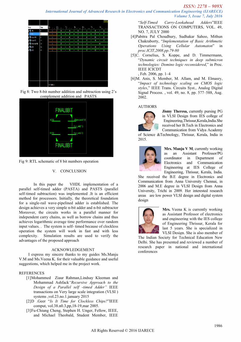
Fig 8: Two 8-bit number addition and subtraction using 2’scomplement addition and PASTS
Fig 9: RTL schematic of 8 bit numbers operation
In this paper the VHDL implementation of aparallel self-timed adder (PASTA) and PASTS (parallelself-timed subtraction) was implemented .It is an efficientmethod for processors. Initially, the theoretical foundationfor a single-rail wave-pipelined adder is established. Thedesign achieves a very simple n-bit adder and n-bit subtractorMoreover, the circuits works in a parallel manner forindependent carry chains, as well as borrow chains and thusachieves logarithmic average time performance over randominput values. . The system is self- timed because of clocklessoperation the system will work in fast and with lesscomplexity. Simulation results are used to verify theadvantages of the proposed approach
ACKNOWLEDGEMENTI express my sincere thanks to my guides Ms.Manju
V.M and Ms.Veena K. for their valuable guidance and usefulsuggestions, which helped me in the project work.
REFERENCES[1]Mohammed Ziaur Rahman,Lindsay Kleeman and
Mohammad Ashfack“Recursive Approach to theDesign of a Parallel self -timed Adder” IEEEtransactions on Very large scale integration (VLSI )systems ,vol.23.no.1.january 2015
[2]D .Geer “Is It Time for Clockless Chips?”IEEEcomput, vol.38.n0.3,pp,18-19,mar 2005.
[3]Fu-Chiung Cheng, Stephen H. Unger, Fellow, IEEE,and Michael Theobald, Student Member, IEEE
“Self-Timed Carry-Lookahead Adders”IEEETRANSACTIONS ON COMPUTERS, VOL. 49,NO. 7, JULY 2000
[4]Pabitra Pal Choudhury, Sudhakar Sahoo, MithunChakraborty, “Implementation of Basic ArithmeticOperations Using Cellular Automaton” inproc.ICIT,2008.pp.79-80
[5]C. Cornelius, S. Koppe, and D. Timmermann,“Dynamic circuit techniques in deep submicrontechnologies: Domino logic reconsidered,” in Proc.IEEE ICICDT, Feb. 2006, pp. 1–4
[6]M. Anis, S. Member, M. Allam, and M. Elmasry,“Impact of technology scaling on CMOS logicstyles,” IEEE Trans. Circuits Syst., Analog DigitalSignal Process. , vol. 49, no. 8, pp. 577–588, Aug.2002.
AUTHORSJismy Theresa, currently pursing PGin VLSI Design from IES college ofEngineering,Thrissur,Kerala,India.Shereceived her B.Tech in Electronics andCommunication from Vidya Academy
of Science &Technology, Thrissur, Kerala, India in2015.
Mrs. Manju V M, currently workingas an Assistant Professor/PGcoordinator in Department ofElectronics and CommunicationEngineering at IES College ofEngineering, Thrissur, Kerala, India.
She received the B.E degree in Electronics andCommunication from Anna University Chennai, in2006 and M.E degree in VLSI Design from AnnaUniversity, Trichi in 2009. Her interested researchareas are low power VLSI design and digital systemdesign
Mrs. Veena K is currently workingas Assistant Professor of electronicsand engineering with the IES collegeof Engineering Thrissur, Kerala forlast 5 years. She is specialized inVLSI Design. She is also member of
The Indian Society for Technical Education NewDelhi. She has presented and reviewed a number ofresearch paper in national and internationalconferences


![M.Sc. Electronicskswu.ac.in/Uploads/Syllabus/PG/Science/M.Sc-Electronics... · 2018-07-24 · 3. a] Implement half adder, half subtractor, full adder and full subtractor using universal](https://static.documents.pub/doc/80x56/5e73386923ac1003d05a8505/msc-2018-07-24-3-a-implement-half-adder-half-subtractor-full-adder-and-full.jpg)


