1Telecommunication Engineering group, University of Twente, PO Box 217, Enschede.7500 AE, the Netherlands 2LioniX BV, PO Box 456, Enschede, 7500 AL, the Netherlands
(060.5625) Radio frequency photonics; (070.6020) Signal processing; (130.3120) Integrated
optics devices; (350.4010) Microwave.
References and links
1. E. I. Ackerman, G. E. Betts, W. K. Burns, J. C. Campbell, C. H. Cox, N. Duan, J. L. Prince, M. D. Regan, and H.
V. Roussell, “Signal-to-noise performance of two analog photonic links using different noise reduction
techniques,” in Proc. IEEE/MTT-S Int. Microwave Symp., pp. 51–54 (2007)
2. D. Marpaung, C. Roeloffzen, and W. van Etten, “Enhanced dynamic range in a directly modulated analog
photonic link,” IEEE Photon. Technol. Lett. 21(24), 1810–1812 (2009).
3. Y. Li, R. Wang, G. Ding, J. Klamkin, L. Johansson, P. Herczfeld, and J. E. Bowers, “Novel phase modulator
linearity measurement,” IEEE Photon. Technol. Lett. 21(19), 1405–1407 (2009).
4. M. J. LaGasse, and S. Thaniyavarn, “Bias-free high-dynamic-range phase-modulated fiber-optic link,” IEEE
Photon. Technol. Lett. 9(5), 681–683 (1997).
5. T. E. Darcie, J. Zhang, P. F. Driessen, and J.-J. Eun, “Class-B microwave- photonic link using optical frequency
modulation and linear frequency discriminators,” J. Lightwave Technol. 25(1), 157–164 (2007).
6. J. Wyrwas, and M. Wu, “Dynamic range of frequency modulated direct-detection analog fiber optic link,” J.
Lightwave Technol. 27(24), 5552–5562 (2009).
7. J. Wyrwas, and M. Wu, “High dynamic range microwave photonic links using maximally linear FIR optical
filters,” OFC/NFOEC, Los Angeles, CA, 2010, paper JWA43.
8. X. Xie, J. Khurgin, J. Kang, and F. Choa, “Compact linearized optical FM discriminator,” IEEE Photon. Technol.
Lett. 14(3), 384–386 (2002).
9. X. Xie, J. Khurgin, J. Kang, and F. Choa, “Ring-assisted frequency discriminator with improved linearity,” IEEE
Photon. Technol. Lett. 14(8), 1136–1138 (2002).
10. F. Liu, T. Wang, Z. Zhang, M. Qiu, and Y. Su, “On-chip photonic generation of ultra-wideband monocycle
pulses,” Electron. Lett. 45(24), 1247–1248 (2009).
11. D. Marpaung, C. Roeloffzen, R. Timens, A. Leinse, and M. Hoekman, “Design and realization of an integrated
optical frequency modulation discriminator for a high performance microwave photonic link,” IEEE Topical
meeting in Microwave Photonics (MWP 2010), Montreal, Canada, 131–134, (2010).
12. F. Morichetti, A. Melloni, M. Martinelli, R. É. G. Heideman, A. Leinse, D. H. Geuzebroek, and A. Borreman,
“Box-shaped dielectric waveguides: A new concept in integrated optics?” J. Lightwave Technol. 25(9), 2579–
2589 (2007).
13. C. G. H. Roeloffzen, L. Zhuang, R. G. Heideman, A. Borreman, and W. van Etten, “Ring resonator-based
tunable optical delay line in LPCVD waveguide technology,” in Proc. IEEE/LEOS Benelux Chapter, 10th Symp.,
pp. 71–74, (2005).
#137011 - $15.00 USD Received 21 Oct 2010; revised 7 Dec 2010; accepted 7 Dec 2010; published 13 Dec 2010(C) 2010 OSA 20 December 2010 / Vol. 18, No. 26 / OPTICS EXPRESS 27359
14. R. G. Heideman, A. Leinse, W. Hoving, R. Dekker, D. H. Geuzebroek, E. J. Klein, R. Stoffer, C. G. H.
Roeloffzen, L. Zhuang, and A. Meijerink, “Large-Scale Integrated Optics using TriPleX Waveguide Technology:
From UV to IR,” Proc. SPIE 7221, 72210R–1 - 72210R–15 (2009).
15. J. Zhang, and T. E. Darcie, “Two-tone analysis of distortion suppression in microwave photonic links using
phase modulation and fiber-Bragg grating filters,” International Symposium on Signals, Systems and Electronics,
Montreal, Quebec, (2007).
16. J. D. McKinney, K. Colladay, and K. J. Williams, “Linearization of phase-modulated analog optical links
employing interferometric detection,” J. Lightwave Technol. 27(9), 1212–1220 (2009).
17. V. Urick, M. Godinez, P. Devgan, J. McKinney, and F. Bucholtz, “Analysis of an analog fiber-optic link
employing a low-biased Mach–Zehnder modulator followed by an erbium-doped fiber amplifier,” J. Lightwave
Technol. 27(12), 2013–2019 (2009).
1. Introduction
Nowadays there are increasing interests towards high performance microwave photonic links
(MPLs) for a number of applications like antenna remoting, radio over fiber and phased-array
antenna. To serve these applications the MPLs need to fulfill several criteria namely high link
gain, low noise figure and high spurious-free dynamic range (SFDR). High SFDR dictates
high linearity and low noise in the MPLs. In intensity modulated direct detection (IMDD)
MPL the SFDR is mainly limited by the laser relative intensity noise (RIN) and the third order
intermodulation distortion (IMD) either from the directly modulated laser or the electro-optic
modulator (EOM). In such IMDD links, the SFDR can be increased in several ways. An MPL
with a Mach-Zehnder EOM benefits from low biasing the EOM that reduces the link noise
[1], while an MPL with directly modulated lasers might achieve high SFDR using balanced
push-pull architecture that removes even-order IMDs in the balanced photodetector [2].
A type of MPL that gains significant interest recently is the phase-modulated direct
detection (PM DD) link. In such a link, a phase modulated signal is converted to intensity
modulation (PM-IM conversion) using an optical discriminator, thereby allowing a simple
direct detection scheme instead of the complicated coherent detection. The interest in such a
scheme stems from two reasons; first, a phase modulator (for example a conventional lithium
niobate PM) can provide high linearity [3] and its operation does not require biasing [4]. The
second reason is that there is an additional degree of freedom in tailoring the characteristic of
the optical filter discriminator to enhance the MPL performance. Thus, in such an approach,
the photonic discriminator is designed for increasing the link linearity and/or suppressing the
noise in the MPL. In previously reported investigations, different filter types have been
proposed as the photonic discriminator [4–9]. The simplest one, being a Mach-Zehnder
interferometer (MZI), suffers from large nonlinearities [4]. Fiber Bragg-gratings (FBGs) have
also been widely considered for the FM discriminator, notably with the potential of noise
reduction [5]. However these FBGs and the circulators needed for such solutions are bulky
and thus, preventing a compact discriminator. Moreover, the FBGs are lacking in
programmability. Integrated optics solutions have also been proposed [6–9] but, to our
knowledge, these are limited to concept and have not been realized yet. On the other hand a
photonic chip approach has been reported for PM-IM conversion albeit for ultrawideband
(UWB) monocycle pulses generation [10].
In this paper, we report a complete design, realization and characterization of a phase
modulation direct detection MPL employing a fully tunable and programmable photonic chip
discriminator. This is for the first time to our knowledge such a photonic chip is employed in
an MPL. The rest of the paper is organized as follows; the MPL architecture and the principle
of operation of the photonic chip are presented in Section 2. The chip fabrication and
packaging is discussed in Section 3. In Section 4 the MPL characterization is thoroughly
presented. The paper closes with conclusions.
#137011 - $15.00 USD Received 21 Oct 2010; revised 7 Dec 2010; accepted 7 Dec 2010; published 13 Dec 2010(C) 2010 OSA 20 December 2010 / Vol. 18, No. 26 / OPTICS EXPRESS 27360
Fig. 1. The schematic of a phase modulation direct-detection microwave photonic link
employing a balanced frequency discriminator photonic chip. BPD: balanced photodetector.
2. The MPL architecture and the photonic chip characteristics
The architecture of the MPL is shown in Fig. 1. The modulated optical signal from a phase
modulator is routed to the receiver site using a single optical fiber. The receiver consists of the
discriminator photonic chip and the balanced photodetector (BPD). The filter has one optical
input and two optical outputs where the ideal transfer functions from the input to the two
outputs are mirror images of each other, as shown in Fig. 1. The transfer function has a sharp
transition at the angular frequency of the optical carrier (ωc). Ideally, at the upper branch, for
frequencies below ωc the magnitude filter response is zero while above the ωc it is linear up to
a maximum frequency. This also applies to the other output for frequencies below ωc. A phase
modulated direct detection MPL with this transfer function falls in the category of a class-B
MPL, initially proposed by Darcie et al. in [5]. The MPL benefits from shot noise and RIN
reduction for SFDR enhancement.
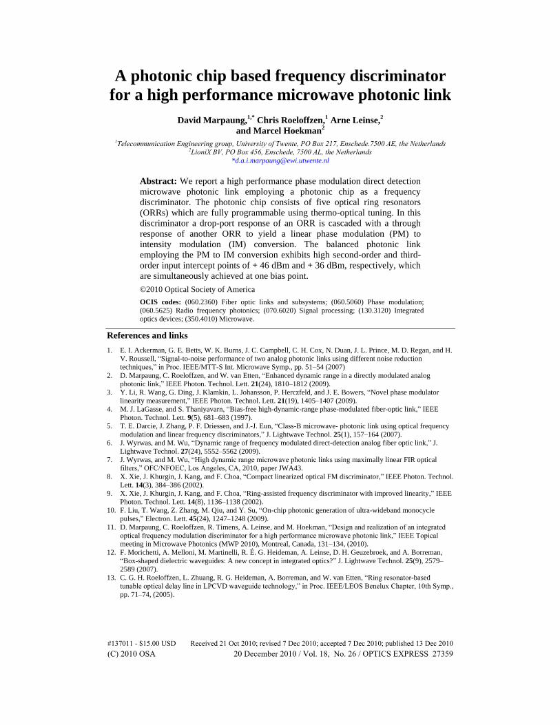
To obtain the desired filter response we use on-chip photonic discriminator consisting of
five optical ring resonators (ORRs) all in an add-drop configuration. The ORRs considered
are racetrack structures connected with a pair of tunable couplers to two straight optical
waveguides, as depicted in Fig. 2. Using heaters placed on top of the ORRs the resonance
frequency and the coupling coefficients (and subsequently the Q-factor) of all ORRs can be
tuned via thermo-optics effects. The principle of operation of the photonic chip is illustrated
with the simulation results depicted in Figs. 2A-2D. A cascade of responses from the through
ports of ORRs is used to linearize and to increase the suppression of a response from a drop
port of another ORR. In this way, one obtains a linear slope for a PM-IM conversion. The
detailed explanation of the chip operation is described in [11]. In this paper, we focus on the
fabrication of the photonic discriminator and the performance of an MPL employing the
discriminator.
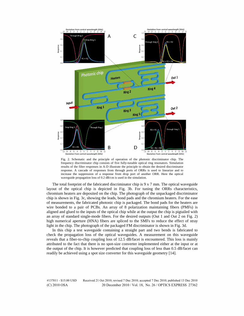
3. Chip fabrication, packaging and characterization
The designed filter is fabricated in the CMOS compatible TriPleXTM waveguide technology
with a high contrast box shaped waveguide structure [12]. The schematic image of the
waveguide structure is shown in the inset of Fig. 3a, where Si3N4 is shown in pink and SiO2 is
shown in blue. The SEM image of the realized waveguide structure is shown in Fig. 3a. The
fabricated ring resonators have a round trip length of 8 mm (16 mm for rings 4 and 5) and the
bend radius of the curved part of the ORR is 150 μm. For this bending radius, the group index
of the lowest order mode for TE polarized light with a wavelength of 1550 nm is simulated to
be 1.746. It can be calculated that the ORRs have a free spectral range of 21.5 GHz (for Rings
1 to 3 and 10.7 GHz for Rings 4 and 5). We measured the propagation loss in the waveguide
with the technique described in [13]. It is assumed that the measurement is dominated by the
waveguide loss instead of the bend loss, as confirmed by simulations. The measured
waveguide loss amounts to 1.2 dB/cm. The loss mainly contributed from sidewall roughness
in the waveguide. This loss directly limits the Q-factor of the resonators. However, we have
recently obtained a propagation loss as low as 0.2 dB/cm with a new waveguide geometry.
The detailed measurements of this propagation loss will be published elsewhere.
#137011 - $15.00 USD Received 21 Oct 2010; revised 7 Dec 2010; accepted 7 Dec 2010; published 13 Dec 2010(C) 2010 OSA 20 December 2010 / Vol. 18, No. 26 / OPTICS EXPRESS 27361
Fig. 2. Schematic and the principle of operation of the photonic discriminator chip. The
frequency discriminator chip consists of five fully-tunable optical ring resonators. Simulation
results of the filter responses in A-D illustrate the principle to obtain the desired discriminator
response. A cascade of responses from through ports of ORRs is used to linearize and to
increase the suppression of a response from drop port of another ORR. Here the optical
waveguide propagation loss of 0.2 dB/cm is used in the simulation.
The total footprint of the fabricated discriminator chip is 9 x 7 mm. The optical waveguide
layout of the optical chip is depicted in Fig. 3b. For tuning the ORRs characteristics,
chromium heaters are deposited on the chip. The photograph of the unpackaged discriminator
chip is shown in Fig. 3c, showing the leads, bond pads and the chromium heaters. For the ease
of measurements, the fabricated photonic chip is packaged. The bond pads for the heaters are
wire bonded to a pair of PCBs. An array of 8 polarization maintaining fibers (PMFs) is
aligned and glued to the inputs of the optical chip while at the output the chip is pigtailed with
an array of standard single-mode fibers. For the desired outputs (Out 1 and Out 2 on Fig. 2)
high numerical aperture (HNA) fibers are spliced to the SMFs to reduce the effect of stray
light in the chip. The photograph of the packaged FM discriminator is shown in Fig. 3d.
In this chip a test waveguide containing a straight part and two bends is fabricated to
check the propagation loss of the optical waveguides. A measurement on this waveguide
reveals that a fiber-to-chip coupling loss of 12.5 dB/facet is encountered. This loss is mainly
attributed to the fact that there is no spot-size converter implemented either at the input or at
the output of the chip. It is however predicted that coupling loss of less than 0.5 dB/facet can
readily be achieved using a spot size converter for this waveguide geometry [14].
#137011 - $15.00 USD Received 21 Oct 2010; revised 7 Dec 2010; accepted 7 Dec 2010; published 13 Dec 2010(C) 2010 OSA 20 December 2010 / Vol. 18, No. 26 / OPTICS EXPRESS 27362
Fig. 3. Realization of the photonic chip discriminator. (a) SEM picture of the box-shaped
optical waveguide cross section. (b) Optical waveguide layout of the discriminator. (c)
Photograph of the photonic chip showing the leads and bondpads of the heaters. (d) The
packaged photonic chip with fiber array units and wirebonded PCBs.
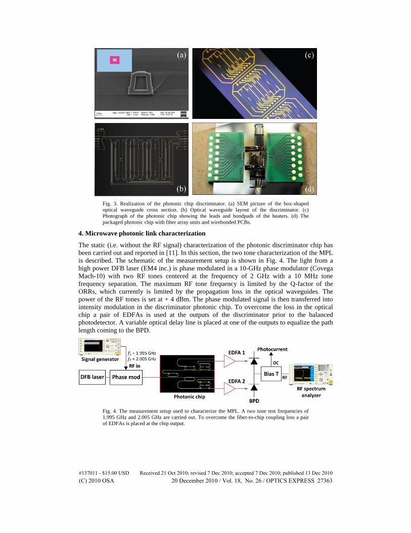
4. Microwave photonic link characterization
The static (i.e. without the RF signal) characterization of the photonic discriminator chip has
been carried out and reported in [11]. In this section, the two tone characterization of the MPL
is described. The schematic of the measurement setup is shown in Fig. 4. The light from a
high power DFB laser (EM4 inc.) is phase modulated in a 10-GHz phase modulator (Covega
Mach-10) with two RF tones centered at the frequency of 2 GHz with a 10 MHz tone
frequency separation. The maximum RF tone frequency is limited by the Q-factor of the
ORRs, which currently is limited by the propagation loss in the optical waveguides. The
power of the RF tones is set at + 4 dBm. The phase modulated signal is then transferred into
intensity modulation in the discriminator photonic chip. To overcome the loss in the optical
chip a pair of EDFAs is used at the outputs of the discriminator prior to the balanced
photodetector. A variable optical delay line is placed at one of the outputs to equalize the path
length coming to the BPD.
Fig. 4. The measurement setup used to characterize the MPL. A two tone test frequencies of
1.995 GHz and 2.005 GHz are carried out. To overcome the fiber-to-chip coupling loss a pair
of EDFAs is placed at the chip output.
#137011 - $15.00 USD Received 21 Oct 2010; revised 7 Dec 2010; accepted 7 Dec 2010; published 13 Dec 2010(C) 2010 OSA 20 December 2010 / Vol. 18, No. 26 / OPTICS EXPRESS 27363
4.1 Nonlinearity
To characterize the filter transfer function, the laser bias current is changed every 0.2 mA. The
change in the central frequency of the laser is measured to be 0.75 GHz/mA. For every bias
current, the power of the signal, second-order (IMD2) and third order (IMD3) intermodulation
products at the frequency of 2.005 GHz, 4.0 GHz and 2.015 GHz, respectively, are measured
in the RF signal analyzer (Agilent MXA N9020A). Meanwhile the detected photocurrent is
measured using a multimeter connected to the DC output of the bias T.
The photonic chip is tuned such that only the drop response of Ring 3 (Fig. 2) is observed
at Out 2 of the chip and no light is coupled to the drop port of Ring 1. The bias current of the
laser is varied from 457 mA to 477 mA, which results in a total frequency shift of 15 GHz.
The measured signal, IMD2 and IMD3 powers as well as the detected photocurrent as
functions of the laser bias current are depicted in Fig. 5a. The corresponding laser frequency
change with respect to the central frequency is also indicated at the top axis of the figure. The
measured photocurrent clearly depicts the drop response of the corresponding ring. The signal
power is maximized in the region where the slope of the response is the highest, which occurs
in the region of 464 mA to 465 mA for the positive slope. As expected the signal power and
subsequently the IMD power are minimized in the region where the peak of the drop response
occurs. This is similar to the characteristic of the Mach-Zehnder modulator (MZM) at the
peak of the transmission point. However, the notable difference with the MZM, in this
demodulation using the drop response there is no bias point where the even-order distortion
product is minimized. Thus only with a drop response an obvious bias point of operation will
be where the signal power is maximized.
Starting from the drop response described earlier, Ring 1 is tuned to the resonance
frequency to yield a through response. By means of tuning the phase shifter on the ring, the
resonance frequency of Ring 1 can be brought closer to the resonance frequency of the drop
from Ring 3. The through response of Ring 1 increases the suppression of the drop response
and, more importantly, linearized the response. This is depicted in Fig. 5b where the RF and
the photocurrent measurement results on the combined drop and through responses are
depicted. The addition of the through response introduces bias regions where the IMD2 and
the IMD3 powers are minimized. The bias point where the IMD2 power is suppressed
coincides with the region where the signal is maximized. As for the IMD3, the “symmetry”
between the signal and the IMD3 is broken, such that the bias point where the IMD3 is
suppressed is off-set from the bias point where the signal extinct. Thus, by introducing the
through response, there are two optimized bias points for the MPL; the one where the IMD2 is
suppressed (at 464.8 mA at Fig. 5b) and the one where the IMD3 is suppressed (at 462.8 mA).
#137011 - $15.00 USD Received 21 Oct 2010; revised 7 Dec 2010; accepted 7 Dec 2010; published 13 Dec 2010(C) 2010 OSA 20 December 2010 / Vol. 18, No. 26 / OPTICS EXPRESS 27364
Fig. 5. Two tone test measurement results depicting signal and IMD powers and the
photocurrent as functions of the laser bias current for (a) Drop response of Ring 3, (b) A
cascade of drop response of Ring 3 and through of Ring 1. (c) A cascade of drop response of
Ring 3 and through responses of Rings 1 and 5. (d) A balanced response from Ring 1, 3 and 5.
The frequency change of the laser is 0.75GHz/mA.
Introducing a second through response from Ring 5 to the previously described response
contributes to the same effect. However, the bias point where the signal extinct is pushed
further from the bias point where the IMD3 product is suppressed (Fig. 5c). Thus, the MPL
biased for minimum IMD3 will have more robustness against bias current instabilities relative
to the previously described link. The main characteristic of this link and the one previously
described is that the bias point where the IMD2 product is minimized does not coincide with
the bias point where the IMD3 is suppressed. In the former, the IMD3 is maximized while in
the latter the IMD2 power is maximized. Thus, the MPL user needs to choose either to
maximize the IMD2 limited SFDR or the IMD3 limited SFDR. In most cases the desired MPL
characteristic is both low IMD2 and IMD3 powers obtained simultaneously at a single bias
point. This characteristic has not been achieved, limited to our knowledge, either with Mach-
Zehnder modulator, electroabsorption modulators or directly modulated laser MPLs. But this
characteristic can be achieved by means of operating the photonic discriminator chip in the
balanced mode, where both the desired outputs of the chip are activated. For this purpose,
Rings 1, 2 and 3 are tuned properly. This means that the through response of Ring 1 is used to
linearized the drop response of Ring 3 at Out 2 of the chip. At the same time, the through
response of Ring 2 is used to linearize the drop response of Ring 1. With this arrangement the
use of a 3-dB optical splitter is avoided. This in principal avoids the unnecessary loss that
occurs in splitting the light from the input into two branches.
#137011 - $15.00 USD Received 21 Oct 2010; revised 7 Dec 2010; accepted 7 Dec 2010; published 13 Dec 2010(C) 2010 OSA 20 December 2010 / Vol. 18, No. 26 / OPTICS EXPRESS 27365
The optical power at the desired outputs are equalized and subsequently detected and
subtracted in the balanced detector. The subtracted photocurrent as well as the signal power
and the IMD products are depicted in Fig. 5d, as evident from this figure, the bias region of
both IMD2 and IMD3 products coincides at approximately 452.4 mA. Thus for this balanced
link, there is a single optimized bias point where both IMD products are suppressed and the
SFDR is maximized.
To determine the linearity improvement obtained by the schemes explained above, the two
tone measurements are repeated for specific bias points and for increasing RF power levels
from 6 dBm up to 10 dBm. From the measured data, the signal, IMD2 and IMD3 powers are
extrapolated to yield the second-order and the third-order input intercept points (IIP2 and
IIP3) defined as the input RF power where the output IMD product power is equal to the
output signal power. The results are summarized in Table 1.
Table 1. MPL characteristics for the responses in Fig. 5
Response Bias current IIP2 IIP3 Photocurrent Noise PSD
(mA) (dBm) (dBm) (mA) (dBm/Hz)
Drop (Fig. 5 a) 464.4 24 25 7.00 135.9
Drop + through (Fig. 5b) 462.8 14 26 4.42 132.8
464.8 36 23 6.37 134.0
3-ring cascade (Fig. 5c) 459.6 23 33 4.50 132.7
461.6 39 24 6.28 134.0
Balanced (Fig. 5d) 452.6 46 36 0.36 131.5
As expected, both the drop + through and the 3-ring cascade responses exhibit two bias
points where the IIP2 and IIP3, respectively, are maximized. The balanced MPL has the
highest IIP2 and IIP3 values relative to the other responses. As a comparison, an MPL with a
Mach-Zehnder modulator with a half-wave voltage (Vπ) of 3 V will yield an IIP3 of +
18 dBm. In such an MPL to achieve a higher IIP3, one must reside to higher half-wave
voltage modulator (Vπ = 20 V for IIP3 = + 36 dBm) which in turn will significantly reduce the
MPL gain (a factor of 16 dB gain reduction relative to the case where Vπ = 3 V). Note that for
the balanced MPL the highest IIP3 can be obtained together with the optimum MPL gain, as
depicted in Fig. 5d. Moreover, in an ideal case where the phase and amplitude of the IMD2
components at each branch of the MPL are matched, the IMD2 product at the BPD output can
be completely suppressed and the MPL will exhibit an infinite IIP2.
4.2 Bandwidth
In order to verify the instantaneous bandwidth of operation of the MPL, the two tone
measurements are performed for different modulation frequencies. Figure 6 shows the
measurement results versus the laser bias current (and the laser frequency change) for the
fundamental tone and the IMD3. In this measurement, the photonic chip is configured to yield
a cascade of a drop response of Ring 1 and a through response of Ring 2 observed at Out 1.
The RF tones power and frequency separation are kept as in the previous measurement but
their central frequency is varied from 1 GHz to 4 GHz with a step of 1 GHz.
#137011 - $15.00 USD Received 21 Oct 2010; revised 7 Dec 2010; accepted 7 Dec 2010; published 13 Dec 2010(C) 2010 OSA 20 December 2010 / Vol. 18, No. 26 / OPTICS EXPRESS 27366
Fig. 6. Two tone test measurement results for a varying RF tone frequency for a Drop +
through response from Out 1 of the photonic chip depicted against the laser bias current. (a)
Fundamental tone. (b) Third order IMD.
In Fig. 6a the fundamental frequency response is shown and a similar response as
observed in Fig. 5b is obtained. At the bias current of 469.2 mA (indicated by the dashed-
line), where the signal is maximized, the fundamental power variation between 1 GHz to
4 GHz is approximately 3 dB. Thus, at this bias point it can be predicted that the 3 dB
bandwidth of the MPL frequency response is 4 GHz. This indicates that instantaneous
bandwidth of operation for the MPL is relatively broad. As mentioned earlier, this bandwidth
is currently limited by the quality factor of the ORRs and can be increased by reducing the
waveguide propagation loss.
In Fig. 6b the IMD3 frequency response is shown. For each modulation frequency the
IMD3 suppression occurs albeit at a slightly shifted bias point with respect to each other. We
believe this indicates that the suppression can be achieved in a broadband manner, as also
suggested in [15] where a similar scheme was investigated. Since the bias point that
minimized the IMD3 is shifted for each frequency, the MPL would be biased at a point where
the IMD3 powers are the same over the entire band. In this case this bias current is 470.8 mA
which is indicated by the dotted-line in Fig. 6. At this bias point the shot noise limited IMD3-
SFDR for frequencies of 1, 2, 3 and 4 GHz are 99 dB∙Hz2/3, 103 dB∙Hz2/3, 101 dB∙Hz2/3, and
101 dB∙Hz2/3, respectively. Thus, within the considered signal band, the SFDR varies by 4 dB.
Thus, the bandwidth of linearization in this MPL is relatively wide. For the sake of
comparison, the SFDR variation in the linearization technique applied in a phase modulated
system reported in [16] is more than 20 dB over a frequency range of 2 GHz.
4.3 Noise
The measured noise power spectral density of the link in the selected bias points are listed in
Table 1. This noise PSD comprises of various noise sources, namely the thermal noise, the
shot noise, relative intensity noise (RIN), amplified spontaneous emission from the EDFA and
the phase noise from the laser that is transferred to intensity noise by the filter. The PSD of the
thermal noise electrical power delivered to a matched load expressed in W/Hz can be written
as,
th MPL B1S g k T (1)
where gMPL is the MPL gain, kB is the Boltzmann constant and T is the ambient temperature in
Kelvin. The shot noise PSD is proportional to the detected photocurrent, Id, and can be written
as
shot d L2S qI R (2)
#137011 - $15.00 USD Received 21 Oct 2010; revised 7 Dec 2010; accepted 7 Dec 2010; published 13 Dec 2010(C) 2010 OSA 20 December 2010 / Vol. 18, No. 26 / OPTICS EXPRESS 27367
where q is the electron charge and RL is the load resistance. The noise contribution from the
EDFA can be regarded as the additional RIN to the system [17]. This is also true for the phase
noise converted to intensity noise [6]. Thus, we define the system RIN (RINsys) as the sum of
the RIN from the laser (RINlaser), the ASE noise (RINASE) and the phase noise (RINphase),
sys laser ASE phaseRIN RIN RIN RIN . (3)
The noise PSD of the system RIN can thus be written as
2
RINsys sys d LRIN .S I R (4)
For a system where a passive impedance matching is imposed on the output of the
photodetector, the total noise PSD is
noise th shot RIN total
1.
4S S S S (5)
Using Eqs. (1), (2), (4) and (5) and the measured values of the noise PSD and the average
photocurrent listed on Table 1, one can extract the value of RINsys for each configuration. In
general, the system suffers from relatively high system RIN. For example, the 3-ring cascade
configuration biased at 459.6 mA RINsys = 126.7 dB/Hz, while at bias current of 461.6 mA
the system RIN reduces to 131 dB/Hz. As mentioned earlier, this system RIN comprises of
the contribution of the laser RIN, the RIN from the EDFA and the additional RIN from phase
to intensity noise conversion in the filter. A measurement performed on the laser shows that
the value of RINlaser biased at the current beyond 450 mA is better than 170 dB/Hz. Thus the
dominant RIN source is either the EDFA or the PM-IM conversion.
In order to separate the contribution from RINASE and RINphase, noise measurements with
and without the discriminator chip were performed and the results are compared. In the latter
measurement, the loss of the photonic chip is emulated by a variable optical attenuator (VOA)
such that the detected photocurrents in both measurements are identical. In the measurement
without the presence of the optical discriminator it can be assumed that the RINphase
contribution is absent. Thus, by means of subtracting the two measurement results, one can
identify the contribution of RINphase to the total system noise. Moreover, given the knowledge
that RINlaser is lower than 170 dB/Hz the other RIN values in Eq. (3) can be determined. The
measured RINsys, RINASE, RINphase and the photocurrent as function of the laser bias current is
depicted in Fig. 7.
Fig. 7. Components of the system RIN extracted from the noise measurements. The RIN
contribution from the laser amounts to 170 dB/Hz.
It is evident from Fig. 7 that the system RIN is dominated by the ASE noise from the
EDFA. The contribution from the phase to intensity noise conversion is smaller relative to the
#137011 - $15.00 USD Received 21 Oct 2010; revised 7 Dec 2010; accepted 7 Dec 2010; published 13 Dec 2010(C) 2010 OSA 20 December 2010 / Vol. 18, No. 26 / OPTICS EXPRESS 27368
EDFA noise but dominates over the laser RIN. This RINphase is proportional to the linewidth
(Δν) of the laser [6], which is in the order of 1 MHz for the DFB laser used in the
experiments. Thus, for a laser with narrower linewidth, the RINphase contribution to the system
noise can be reduced. As an example, with a laser with a linewidth of 5 kHz, which is already
commercially available, the RINphase can be reduced from 145 dB/Hz to 168 dB/Hz.
4.4 Spurious-free dynamic range (SFDR)
The IMDn-SFDR is defined as the signal-to-noise ratio in a 1-Hz bandwidth for the input
power where the power of the IMDn product is equal to the noise power. Here n = 2 for the
second-order IMD or n = 3 for the third-order IMD. The IMDn-SFDR can be expressed in
terms of the MPL n-th order input intercept point and the noise PSD via the relation
MPL noise
1IMD -SFDR IIP dBm/Hz .
nn n G S
n
(6)
where GMPL is the MPL link gain expressed in decibels and the noise PSD is expressed in
dBm/Hz. The IMD2-SFDR and the IMD3-SFDR for the balanced configuration biased at
452.6 mA (Fig. 5d) is depicted in Fig. 7. Here, two values of the noise PSD are used; the
measured value using the setup in Fig. 4, where two EDFAs are used, and the predicted value
in arrangement where the EDFAs are removed and a laser with better linewidth (Δν = 5 kHz)
is used.
Fig. 8. The measured SFDR for the balanced MPL biased at 452.6 mA (Fig. 5d). The
measured values correspond to the measured noise PSD of 131 dBm/Hz while the predicted
values are calculated with noise PSD of 166 dBm/Hz.
As evident from Fig. 8, the balanced MPL exhibit only moderate values of IMD2-SFDR
and IMD3-SFDR which are 73 dB∙Hz1/2 and 90 dB∙Hz2/3, respectively. This is due to the high
system RIN which results in a high noise PSD in the MPL. This effects stems from the high
losses in the chip, mainly contributed from the fiber-to-chip coupling loss (12.5 dB/facet).
Although a relatively high power laser is used (Plaser > 100 mW) the losses in the chip dictate a
use of two EDFAs prior to the BPD, which will introduce a high RINASE in the system, as
suggested in Fig. 7. Although the loss does not influence the IIP characteristics of the MPL
and the use of EDFA improves the MPL gain, the MPL noise figure is severely deteriorated.
Thus, one can expect a significant improvement in the MPL SFDR if the effect of RINASE can
be removed from the MPL. This can be done by reducing the fiber-to-chip coupling such that
solely using a high power laser is enough to achieve a sufficient MPL gain.
In Table 2, the predicted SFDR values of the balanced MPL in various cases are listed
together with the measured values (Case 1). Supposed that the fiber-to-chip coupling loss can
#137011 - $15.00 USD Received 21 Oct 2010; revised 7 Dec 2010; accepted 7 Dec 2010; published 13 Dec 2010(C) 2010 OSA 20 December 2010 / Vol. 18, No. 26 / OPTICS EXPRESS 27369
be reduced significantly, the EDFAs can be removed while keeping the MPL gain and the
photocurrent the same as the measured values. In this case, the noise PSD is reduced by 19 dB
relative to the measured value. The RINsys in this case is dominated by RINphase (related to Δν
= 1 MHz), which amounts to 145 dB/Hz. As predicted in Eq. (6), a 19 dB improvement in
the noise PSD will translate to roughly 9 dB and 12 dB of IMD2-SFDR and IMD3-SFDR
improvements, respectively (case 2). In the third case, a lower linewidth laser is considered
(Δν = 5 kHz) as the source. In this case, the RINphase contribution (168 dB/Hz) is comparable
to the RINlaser contribution (170 dB/Hz). The noise PSD, IMD2-SFDR and IMD3-SFDR are
improved by 16 dB, 8 dB and 11dB, respectively. Finally, in the fourth case a shot noise
limited MPL. This corresponds to the situation where the RINsys is suppressed in the BPD as
in an ideal situation where the optical path lengths to the BPD are perfectly matched [1]. In
this case the calculated noise PSD is roughly the same as in the third case. Thus, if a laser with
RIN as low as 170 dB/Hz and a linewidth of 5 kHz is used in the MPL, the system will be
shot noise limited. The resulting IMD2 and IMD3-SFDRs are shown as the predicted values
in Fig. 8.
Table 2. Calculated SFDR for various cases (RINlaser = 170 dB/Hz)
# Case RINsys Noise PSD IMD2-SFDR IMD3-SFDR
(dB/Hz) (dBm/Hz) (dB∙Hz1/2) (dB∙Hz2/3)
1 EDFA is used; Δν = 1 MHz 127 131 73 90
2 No EDFA; Δν = 1 MHz 145 150 82 102
3 No EDFA; Δν = 5 kHz 168 166 90 113
4 Shot noise limited - 166.5 90 113
A further improvement to the system performance can be expected with a current
technology that leads to a novel optical waveguide with a propagation loss below 0.2 dB/cm
and employing a spot size converter in the discriminator chip to reduce the fiber-to-chip
coupling loss to below 0.5 dB/facet. In this way, and using a better laser source, an ultra high
SFDR can be demonstrated. Moreover, with low loss photonic discriminator the concept of
class-B optical link, where the shot noise reduction is also expected can be demonstrated.
5. Conclusions
The design, fabrication and characterization of a photonic chip frequency discriminator have
been reported. Cascading a through response of an ORR to drop response of another ORR will
yield a linear response. A phase-modulated direct detection MPL employing this photonic
discriminator chip exhibit IIP2 and IIP3 of 46 dBm and 36 dBm, respectively. Improving the
laser characteristics (RINlaser = 170 dB/Hz, Δν = 5 kHzϛ) and reducing the fiber-to-chip
coupling loss will lead to a high SFDR of 113 dB∙Hz2/3. Further improvement can be expected
with the current chip technology with the waveguide propagation loss below 0.2 dB/cm and
using a spot-size converter to reduce the coupling loss to below 0.5 dB/facet.
Acknowledgment
The research described in this paper is partly funded by the European Commission in the 7th
Framework Program. The SANDRA project is a Large Scale Integrating Project for the FP7
Topic AAT.2008.4.4.2 (Integrated approach to network centric aircraft communications for
global aircraft operations).
#137011 - $15.00 USD Received 21 Oct 2010; revised 7 Dec 2010; accepted 7 Dec 2010; published 13 Dec 2010(C) 2010 OSA 20 December 2010 / Vol. 18, No. 26 / OPTICS EXPRESS 27370