50
Philips Semiconductors TP97036.2/W97 TRAD APPLICATION NOTE A printer adapter power supply for 90 Watt peak with TEA1532 AN10316_1

Philips Semiconductors
TP97036.2/W97 TRAD
APPLICATION NOTE
A printer adapter power supply for 90 Watt peak with TEA1532
AN10316_1

A printer adapter power supply for 90 Watt peak with TEA1532
Application Note
AN10316_1
Philips Semiconductors
2
This application note describes a typical printer / notebook adapter power supply, based on a GreenchipTMII controller, the TEA1532. The features of this controller are elaborated in full detail and a possible design strategy for both discontinuous and continuous conduction mode is given to obtain the basic component values. This is demonstrated by the example design of an adapter power supply.
Abstract
© Royal Philips Electronics N.V. 2004 All rights are reserved. Reproduction in whole or in part is prohibited without the prior written consent of the copy-right owner. The information presented in this document does not form part of any quotation or contract, is believed to be accurate and reliable and may be changed without notice. No liability will be accepted by the publisher for any consequence of its use. Publication thereof does not convey nor imply any license under patent- or other industrial or intellectual property rights.
© Royal Philips Electronics N.V. 2004 All rights are reserved. Reproduction in whole or in part is prohibited without the prior written consent of the copy-right owner. The information presented in this document does not form part of any quotation or contract, is believed to be accurate and reliable and may be changed without notice. No liability will be accepted by the publisher for any consequence of its use. Publication thereof does not convey nor imply any license under patent- or other industrial or intellectual property rights.

A printer adapter power supply for 90 Watt peak with TEA1532
Application Note
AN10316_1
Philips Semiconductors
3
APPLICATION NOTE
A printer adapter power supply for 90 Watt peak with TEA1532
AN10316_1
Author(s): Hans Verhees
Kees Schetters [email protected]
Philips Semiconductors
Business Unit Power Management Product Line Integrated Power
Nijmegen The Netherlands
Keywords
TEA1532 GreenchipTMII
Flyback converter Quasi resonant
Continuous conduction mode Low power standby
Valley locking Printer adapter
Date: 2004-06-10
Number of pages: 50

A printer adapter power supply for 90 Watt peak with TEA1532
Application Note
AN10316_1
Philips Semiconductors
4
The present application note describes a typical printer / notebook adapter power supply, based on a GreenchipTMII controller, the TEA1532. The features of this controller are elaborated in full detail and a possible design strategy is given to obtain the basic component values. This is demonstrated by two example designs of a printer adapter power supply: one design operates always in discontinuous conduction mode, while the other one changes smoothly to continuous conduction mode at the high end of the output power range. The design is laid out for a continuous output power of 60 Watt with a peak power capability of 90 Watt. Finally, measurement results and waveforms and a fault finding tree help locate problems.
Summary

A printer adapter power supply for 90 Watt peak with TEA1532
Application Note
AN10316_1
Philips Semiconductors
5
TABLE OF CONTENTS
1. INTRODUCTION.....................................................................................................................................7
2. FUNCTIONAL DESCRIPTION OF THE TEA1532 ............................................................................9
2.1 General description .............................................................................................................................9 2.2 Start-up sequence ...............................................................................................................................9 2.3 Safe-restart mode..............................................................................................................................11 2.4 Operating modes...............................................................................................................................11
2.4.1 Discontinuous conduction mode...........................................................................................12 2.4.2 Continuous conduction mode ...............................................................................................12
2.5 Low Power mode...............................................................................................................................13 2.6 Protections ........................................................................................................................................13
2.6.1 Mains enabling threshold level .............................................................................................13 2.6.2 Brown out Protection ............................................................................................................13 2.6.3 Over current protection .........................................................................................................14 2.6.4 Soft start................................................................................................................................14 2.6.5 Maximum on-time .................................................................................................................14 2.6.6 Maximum duty cycle .............................................................................................................14 2.6.7 Demagnetization ...................................................................................................................14 2.6.8 Over temperature protection on the die................................................................................14 2.6.9 Vcc under voltage lock-out level ............................................................................................15 2.6.10 Protect pin.............................................................................................................................15
2.7 IC pin description...............................................................................................................................16
3. DESIGN OF AN ADAPTER SUPPLY FOR GLOBAL MAINS IN DCM........................................17 3.1 Introduction to design ........................................................................................................................17 3.2 Supply specification...........................................................................................................................17 3.3 Design data .......................................................................................................................................19 3.4 Input and output power .....................................................................................................................19 3.5 Main supply capacitor........................................................................................................................19 3.6 Transformer turns ratio......................................................................................................................20 3.7 Maximum duty cycle..........................................................................................................................20 3.8 Transformer primary inductance .......................................................................................................21 3.9 Transformer definition .......................................................................................................................22 3.10 Auxiliary winding................................................................................................................................22
3.10.1 dV/dt Limiter (resonance capacitor)......................................................................................22 3.11 Driver output and dissipation of the MOSFET ..................................................................................22
3.11.1 Switching losses ...................................................................................................................23 3.11.2 Conduction losses.................................................................................................................23 3.11.3 Total losses...........................................................................................................................24
3.12 Current sense resistor .......................................................................................................................24 3.13 Soft-start circuit .................................................................................................................................24 3.14 Peak clamp........................................................................................................................................25 3.15 Demag sensing .................................................................................................................................26 3.16 Brown out protection .........................................................................................................................26 3.17 Over temperature protection .............................................................................................................26 3.18 Over voltage protection .....................................................................................................................27 3.19 VCC supply .........................................................................................................................................27 3.20 Secondary diode ...............................................................................................................................27 3.21 Secondary capacitor..........................................................................................................................28

A printer adapter power supply for 90 Watt peak with TEA1532
Application Note
AN10316_1
Philips Semiconductors
6
3.22 Voltage feedback circuit ....................................................................................................................28 3.22.1 Error amplifier .......................................................................................................................28 3.22.2 Opto-coupler .........................................................................................................................29 3.22.3 Loop response ......................................................................................................................29
3.23 Miscellaneous....................................................................................................................................29 3.24 Complete circuit diagram ..................................................................................................................30
4. DESIGN OF AN ADAPTER SUPPLY FOR GLOBAL MAINS IN CCM........................................31 4.1 Introduction to design ........................................................................................................................31 4.2 Transformer turns ratio......................................................................................................................31 4.3 Maximum duty cycle..........................................................................................................................31 4.4 Primary peak current .........................................................................................................................32 4.5 Transformer definition .......................................................................................................................32 4.6 Auxiliary winding................................................................................................................................33 4.7 Power switch .....................................................................................................................................33
4.7.1 Switching losses ...................................................................................................................33 4.7.2 Conduction losses.................................................................................................................33 4.7.3 Total losses...........................................................................................................................34
4.8 Current sense resistor .......................................................................................................................34 4.9 Over voltage protection .....................................................................................................................34 4.10 Vcc supply ..........................................................................................................................................34 4.11 Secondary diode ...............................................................................................................................34 4.12 Secondary capacitors........................................................................................................................35 4.13 Loop response...................................................................................................................................35 4.14 Complete circuit diagram ..................................................................................................................37
5. MEASUREMENTS.................................................................................................................................38
5.1 Discontinuous conduction mode .......................................................................................................38 5.1.1 Start up .................................................................................................................................38 5.1.2 Ripple rejection .....................................................................................................................38 5.1.3 Pulse load .............................................................................................................................39 5.1.4 Drain voltage and current .....................................................................................................39 5.1.5 Output short circuit................................................................................................................40 5.1.6 Efficiency...............................................................................................................................40
5.2 Continuous conduction mode............................................................................................................40 5.2.1 Start up .................................................................................................................................40 5.2.2 Ripple rejection .....................................................................................................................41 5.2.3 Pulse load .............................................................................................................................41 5.2.4 Drain voltage and current .....................................................................................................42 5.2.5 Output short circuit................................................................................................................42 5.2.6 Efficiency...............................................................................................................................43
6. FAULT FINDING TREE .......................................................................................................................44
6.1 Main tree ...........................................................................................................................................44 6.2 Output tree ........................................................................................................................................45 6.3 MosFet stage tree .............................................................................................................................45 6.4 Vcc tree .............................................................................................................................................46 6.5 Feedback loop tree............................................................................................................................47
7. REFERENCES........................................................................................................................................48
8. APPENDIX 1: BROWN OUT IN CONTINUOUS CONDUCTION MODE. ...................................49

A printer adapter power supply for 90 Watt peak with TEA1532
Application Note
AN10316_1
Philips Semiconductors
7
1. INTRODUCTION The TEA1532 is a new member of the GreenChipTMII family. This switched mode power supply controller has all the outstanding features of the present range of GreenChipTMII controllers plus some new features: a versatile protection pin and the choice of operating in discontinuous or continuous conduction mode. The GreenChipTMII (TEA1507, TEA1532) is a variable frequency SMPS controller designed for a Quasi-Resonant flyback converter operating directly from the rectified universal mains. The topology is in particular suitable for TV and Monitor Supplies, but can be used for high efficient Consumer Electronics SMPS as well. Applications with the TEA1532 can operate either in discontinuous conduction mode or continuous conduction mode. In the discontinuous conduction mode, the controller operates in quasi resonant mode. This means that the power switch is always switched on in the valley of the resonant waveform of the Drain voltage; peak current as well as switching frequency vary depending upon output load and input voltage. This leads to the lowest possible switching losses. A novel feature of this controller is the fact that the switching behavior is such that under most conditions, the power switch will be switched on in the same valley every period again. The result of this "locked-valley" feature is that the possible low-frequency noise, due to changing valley every period, is avoided. This means that the transformer can be made as cheap as possible without the risk of audible noise. In continuous conduction mode, the controller operates in fixed frequency mode. When the output load drops, the controller will smoothly change to discontinuous mode; the cross-over point is determined by the design of the transformer and the actual input voltage. The control method used in the GreenChipTMII is of the Current Mode Control type. This method inherently compensates for variations of the input voltage (100 Hz ripple rejection). The control loop compares the sensed primary current with the error voltage that is present on the Ctrl pin (VCTRL) to generate the primary "on" time. For low output power, the Reduced Frequency Mode of Operation is used: the controller runs at the minimum on-time, and the output power is controlled by varying the switching frequency. By reducing the switching frequency, the switching losses are reduced to a minimal value. For even lower output powers, stand-by and no-load condition, the controller will enter the cycle skipping mode: the controller will skip cycles i.e. the power switch will not be turned on, if the control loop identifies the output voltage is still high enough. This feature enables the possibility for "no load" power consumption levels below 300mW with no additional circuitry needed. The key features of the GreenChipTMII are summarized below in no special order: Distinctive features
o Operates from universal mains input 90 –265 VAC o High level of integration leads to a very low external component count o Soft (re-) Start to prevent audible noise (externally adjustable) o Leading Edge Blanking (LEB) for current sense noise immunity o Mains dependent operation enabling level (Mlevel; externally adjustable) o Choice of discontinuous QR or continuous FF mode of operation
Green features
o On-chip start-up current source, which is switched "off" after start-up to reduce the power consumption

A printer adapter power supply for 90 Watt peak with TEA1532
Application Note
AN10316_1
Philips Semiconductors
8
o Valley (zero/low voltage) switching for minimal switching losses o Valley locking to prevent audible noise with varying input voltage (ripple) o Frequency Reduction at low output powers for improved system efficiency (output power <
2W) o Cycle skipping mode operation for extremely low power levels
Protection features
o Safe-Restart mode for system fault conditions o Under Voltage Protection (UVLO) for foldback during overload o Continuous mode protection by means of demagnetization detection (only in discontinuous
mode) o Brown-out Protection (external adjustable; only in discontinuous mode) o Cycle-by cycle Over Current Protection (OCP) o Maximum Ton (discontinuous mode) / maximum duty-cycle (continuous mode) Protection o Over Temperature Protection (OTP) o Separate Protection input pin for detection of open loop, over-voltage, over temperature with
latch function. These features enable the power supply engineer to design a reliable and cost effective SMPS with a minimum number of external components and the possibility to deal with the high efficiency requirements.

A printer adapter power supply for 90 Watt peak with TEA1532
Application Note
AN10316_1
Philips Semiconductors
9
2. FUNCTIONAL DESCRIPTION OF THE TEA1532
2.1 General description The TEA1532 GreenchipTMII SMPS control IC is a current mode control IC. It can start up from the rectified mains voltage by means of an internal current source. The control pin, fed with information from the output voltage, compares this with the peak current in the primary winding of the transformer; this determines the on-time of the output driver. The driver stage can drive an external power switch. For discontinuous conduction mode operation, the IC senses the auxiliary voltage to determine the state of the transformer. In continuous conduction mode, this demagnetization sensing is suppressed by connecting the appropriate pin to ground. The peak current in the transformer is limited to a safe value by the Over Current Protection, using the current sense level information. An open loop is detected by sensing the voltage level of the control pin: outside the normal range, a current source in the protect pin is activated. This is timed and eventually causes a safe restart. In case the input voltage drops below a critical value, the IC, operating in discontinuous conduction mode, senses this and performs a safe restart. In discontinuous conduction mode, the maximum on-time is restricted to prevent abnormal behavior. In continuous conduction mode, the maximum duty-cycle is limited. In both cases, the fact will cause a safe restart. A special feature of the TEA1532 is the valley locking facility. This behavior refers to the quasi-resonant switching of the output stage in discontinuous conduction mode where the controller decides to operate at a certain frequency with an applicable peak current depending upon input voltage and output power. This may cause the power switch to be switched on in the first, second, third, etc valley of the resonant waveform at the drain of the power switch. When different valleys are used each period, this can cause audible noise in the transformer due to the modulation of the current (that will cause varying magnetization levels which can be heard with less well glued transformer core-halves). The TEA1532 however will not change the valley over a wider range of input voltage variation and output power and can therefore be used with cheaper transformers without the risk of audible noise.
2.2 Start-up sequence As soon as the rectified line voltage VDC has increased up to the Mains Dependent Operation Level (Mlevel), the internal Mlevel switch will be opened and the high voltage start-up current source will be enabled. This current source will charge the VCC capacitor as depicted in Figure 1. The soft start switch is closed at the moment the VCC capacitor voltage level reaches 7V (typ.). This level initiates the charging of the soft start capacitor CSS, up to a voltage level of 500mV with a typical current of 60µA. In the mean time the charging of the VCC capacitor is continued by the internal high voltage current source in order to reach the VCC start-up level. Once the VCC capacitor is charged to the start-up voltage level (11V typical) the TEA1532 controller starts driving the external power switch and both the high voltage and the soft start current sources are switched off. Resistor RSS will discharge the soft start capacitor CSS, resulting in an amplitude increase of the primary peak current to its steady state value in normal mode of operation. This smooth transition in current level will limit audible noise caused by magnetostriction of the transformer core material. The time constant of the voltage decrease across CSS, which is representing the increase of the primary peak current, can be controlled with the RC combination RSSCSS.

A printer adapter power supply for 90 Watt peak with TEA1532
Application Note
AN10316_1
Philips Semiconductors
10
Vin
V-protect
Vcurrent sense
Vcc
M-level
Vcc-start
520 mV
2.5 Volt
T1 T2 T3 T4 T5
GND
GND
GND
GND
Figure 1: Start up procedure
T1: input power is applied. T2: Mlevel is reached. T3: Vcc reaches the start up level. T4: the auxiliary Vcc winding takes over. T5: output voltage is stable. The soft start time and the time to reach a stable output voltage may be different, depending upon application and output load.
Maximum advantage of the soft start feature can be gained by determining RSS such that the capacitor CSS charges to the maximum voltage of 500 mV: This is the minimum value for RSS to start with peak currents near zero. A higher value for this resistor increases the soft start time (at constant CSS) or decreases the value of the soft start capacitor CSS (at constant soft start time). The maximum value of RSS should be kept below 100 kΩ to prevent problems with offset voltage. A suitable value for CSS is between 47 and 470 nF. The lower limit however is only determined by the demand that the resistor RSS must be short-circuited by this CSS in order to prevent any delay from the current sense signal to the sense input of the IC. The higher limit is the maximum time before the VCC is taken over by the auxiliary winding before under voltage lock out is reached. With the given range of CSS values and a resistor value of 12 kΩ, the soft start time is between (CSS discharged to 10% of the start value): By increasing RSS, the soft start time can be further increased. The discharging of CSS should be chosen such that the supply voltage VCC is taken over by the transformer winding before the supply voltage has dropped below the under voltage lock out level. The VCC capacitor therefore must be chosen such that the supply voltage level does not drop below the under voltage lock out level. The VCC capacitor value shown in the table above is based upon a maximum load current of 1.5 mA and a minimum hysteresis (start up voltage minus under voltage lock out). It must be noted here however that this time is not the complete start up time. This period is the part where the primary current slowly increases to its maximum value. If the output voltage then is still below the desired value, the converter will run on maximum current until the nominal output voltage is reached. There are however some extra requirements for the VCC capacitor. This capacitor must also be able to maintain the supply voltage under extreme low load conditions where the controller enters the cycle
mstmsCRt SSSSSSSS 133.13.2 ≤≤⇒××=
Ω>⇒=> kRA
mVI
VR SS
SSSS 33.8
60500max
µ

A printer adapter power supply for 90 Watt peak with TEA1532
Application Note
AN10316_1
Philips Semiconductors
11
skipping mode. Therefore the value must not be chosen too low to prevent an under voltage lock out situation.
2.3 Safe-restart mode The safe restart mode is entered when the device is triggered by an abnormal condition. These conditions will be explained in chapter 2.6. The effect of entering this mode is:
o The output driver is forced continuously low o The VCC capacitor will gradually discharge to the under voltage lock out level o The high voltage current source is switched on to charge the VCC capacitor again to the
start level o The IC starts again.
If the error persists, the safe restart will be repeated until the error is removed or the input voltage drops below the minimum level.
2.4 Operating modes The controller can operate in two modes, the discontinuous conduction mode and the continuous conduction mode. Apart from changes in values of various components, the designer can select the operating mode by means of the following two pins: Pin nr. Name Discontinuous Continuous 4 Control To emitter opto-coupler Via slope comp. resistor to em. o/c 5 Demagnetization Via resistor to VCC winding To ground 8 Drain To midtap of primary winding To DC supply voltage The continuous conduction mode smoothly changes to discontinuous conduction when the output load drops. This is illustrated in the next figure:
65
F (k
Hz)
Power
QR first valley
QR third valley
QR second valley
FF DCM FF CCM
Cycle
skippingOCP
QR fourth valley
Figure 2: Frequency versus Power

A printer adapter power supply for 90 Watt peak with TEA1532
Application Note
AN10316_1
Philips Semiconductors
12
The figure shows the operating frequency as a function of the input power (i.e. the power delivered by the mains smoothing capacitor). In continuous conduction mode, the operating frequency is fixed at 65 kHz. In discontinuous conduction mode, the frequency varies depending upon the input voltage and the input power. As can be seen in the figure, one input power can be delivered at various operating frequencies using the first, second, third, etc. valley to switch the power switch on again. This depends upon the input voltage and the valley that is used to switch on the power switch. The line OCP represents the over current protection limit at the right hand side. No operation is possible on the right hand side of this line. If a load is slowly increased, the circuit will persist operating in the same valley up to the point where the over current protection is hit. The IC will then reset the valley counter and again search for a valid operating mode. This will result in a lower valley number count and a corresponding new frequency and peak current. The calculation of the inductance of the primary winding in case of a discontinuous conducting transformer is done for a point on the line “valley = 1”, close to the OCP line and close to the maximum frequency line. The additional constraints here are minimum input voltage (minus ripple voltage) and maximum output power. For a continuous conduction transformer design, the inductance of the primary winding is determined by the minimum output power that has to be delivered in continuous conduction mode at maximum input voltage.
2.4.1 Discontinuous conduction mode In the discontinuous conduction mode the current in the primary winding of the transformer returns to zero every cycle again before a new cycle begins. The controller senses the magnetization of the transformer by means of a resistor connected between the auxiliary VCC winding and the demagnetization input. The controller will only start a new cycle after the transformer core has fully demagnetized and a valley is sensed on the drain pin 8. In this mode the transferred power of the converter equals: FILP ppout ***5.0 2= Lp primary inductance of the transformer
Ip peak current in the primary winding of the transformer F the operating frequency
This formula can be rewritten as follows:
p
sout L
TUP
*2** 22 δ
= Lp primary inductance of the transformer Us supply voltage on top of the primary winding of the
transformer T the period time d the duty cycle of the converter
The drain pin of the controller is connected to a tap of the primary winding to enable the valley switching: the controller recognizes the valleys (the minimum voltage level) present on the drain of the power switch and will switch on the power switch in the valley for the lowest possible switching losses. The frequency can vary between 30 and 65 kHz in this mode, depending upon the load and the input voltage.
2.4.2 Continuous conduction mode In the continuous conduction mode, connecting pin 5 to ground disables the sensing of the demagnetization of the transformer core. The operating frequency is now fixed to 65 kHz. In this mode the output power is given by the following formula:

A printer adapter power supply for 90 Watt peak with TEA1532
Application Note
AN10316_1
Philips Semiconductors
13
p
sstsout L
TUIUP
*2**
**22 δ
δ += Lp primary inductance of the transformer Us supply voltage on top of the primary winding of the
transformer Ist value of the primary current at start of the period T the period time d the duty cycle of the primary stroke of the converter
From this equation, one can see that, for the same output power and operating conditions, the primary inductance of the transformer in CCM is (much) larger than in DCM.
2.5 Low Power mode When the required output power drops, the frequency of the converter, operating in discontinuous conduction mode, will automatically increase (while reducing the duty cycle) until the maximum frequency of 65 kHz is reached. At this point only the duty cycle will be further decreased until the minimum possible on-time is reached. With a minimum on-time of 500 ns, the minimum amount of energy per cycle is determined. This means that for an even lower output power the frequency will be reduced. In continuous conduction mode, the frequency is fixed at 65 kHz. This means that only the duty cycle can be reduced to decrease the output power. At a certain power the circuit will smoothly change over to discontinuous conduction mode. At the minimum on-time, the frequency will be reduced to enable the decreasing output power.
2.6 Protections The TEA1532 is equipped with a number of protections to safeguard the application.
2.6.1 Mains enabling threshold level This function safeguards the application for an unwanted start-up at too low input voltages. The typical level is 80 VDC, measured on the drain pin 8 of the IC. This level is called the Mlevel. The level can be shifted upwards however by inserting a series resistor with this pin, due to the fact that this pin also carries the start-up current. The voltage across the series resistor in fact decreases the actual voltage on pin 8 with respect to the voltage across the main supply capacitor. In other words, the voltage for start-up as measured on the main supply capacitor is increased. The following formula shows this: With a typical Ii(Drain) of 1.2 mA, a resistor of 8.2 kΩ will increase the Mlevel with 10 Volt. Once the input voltage has crossed the Mlevel the circuit becomes inactive. This means that when the input voltage, after starting up, drops below the Mlevel, the IC will not stop operating.
2.6.2 Brown out Protection The brown out protection is realized via the demagnetization winding and is therefore not active during continuous conduction mode. This can be overcome with some extra components to realize brown out protection in continuous conduction mode also. The demagnetization sensing resistor is connected between the auxiliary winding and the demag pin 6 of the IC. During the primary stroke of the conversion cycle, the transformed input voltage is present across the auxiliary winding. This causes a defined current in the demag resistor, since the voltage at the IC pin is clamped at approximately -250 mV. The IC measures the current flowing out of the pin, which can be chosen by the designer by means of the resistor value. The current actually represents
8_)(_._ pinserieDrainiICLevelApplLevel RIMM ×+=

A printer adapter power supply for 90 Watt peak with TEA1532
Application Note
AN10316_1
Philips Semiconductors
14
the amplitude of the input voltage and is therefor compared to a reference current in the IC. The current representing the input voltage must be larger than the reference current, otherwise the IC will shut down. In this way, the IC prevents the converter from operating at too low input voltages. The designer can choose the value of the resistor and in doing so, he chooses the minimum operating voltage. It is advised to choose the minimum operating voltage below the Mlevel. Otherwise there is an area where the IC tries to start-up but immediately is stopped again, depending upon the decrease in drain voltage pin 8 due to series impedance. This will cause a repeated start-up / shut down / safe-restart condition.
2.6.3 Over current protection The sense input is connected to the current sensing resistors to close the current control loop. This pin is in the IC also connected to the over current protection comparator. At an input level of 520 mV, the driver is switched in the low state to prevent too high currents in the output stage. The over current protection function incorporates a so called “Leading Edge Blanking” to prevent the function from triggering at the spike at the start of each stroke. This implies that the application does not need any filter at the input. This improves the protection function because there is no delay anymore between actual current and the sense signal.
2.6.4 Soft start Before the IC starts up, a current is sourced out of the sense pin 6. This current can be used to charge a capacitor in the current sensing circuit. The voltage across the capacitor is then effectively lowering the current sense level, in fact lowering the maximum peak current during start-up. By gradually discharging the voltage across aforementioned capacitor, the soft start is realized after which the normal current protection level is applicable.
2.6.5 Maximum on-time In discontinuous conduction mode, the converter is protected for too long on times by an internal maximum timer. This timer will shut down the converter whenever the on-time exceeds the internal limit. When this situation is recognized, the IC will perform a safe restart.
2.6.6 Maximum duty cycle In continuous conduction mode, the converter is protected for too long duty cycles by an internal maximum timer. This timer will shut down the converter whenever the duty cycle exceeds the internal limit. When this situation is recognized, the IC will perform a safe restart.
2.6.7 Demagnetization The demagnetization sensing prevents the converter from running in continuous conduction mode by sensing the magnetization state of the transformer.
2.6.8 Over temperature protection on the die The IC has a built in temperature protection. When the temperature of the die exceeds 140 °C, the IC will shut down. The die temperature then has to drop at least 8 °C before a new start-up is performed. The new start up is only possible after the input voltage has dropped below the Mlevel.

A printer adapter power supply for 90 Watt peak with TEA1532
Application Note
AN10316_1
Philips Semiconductors
15
2.6.9 Vcc under voltage lock-out level The supply voltage of the IC is monitored continuously. When the VCC drops below the under voltage lock out level VCC(UVLO) the IC stops immediately assuming a fault condition. A safe restart is performed:
o The power switch is imediately shut off. o The high voltage start up current source is enabled to charge the VCC capacitor to the start
level. o The soft start circuit in the current sense circuit is enabled. o Switching of the power switch is enabled.
If the error persists, the above sequence is repeated.
2.6.10 Protect pin The protect pin can be used in two different manners:
o Open loop protection timer pin o Input for external protection circuits.
The open loop protection timer functions as follows: An internal comparator monitors the voltage on the control pin. This comparator has a reference voltage of 630 mV. In case the control voltage drops to a level below this threshold, a current is sourced out the protect pin. This current indicates an abnormal level on the control pin, for instance an open feedback loop or an overload condition. These conditions can normally happen for short intervals without damaging the circuit. However if this situation continues, it is assumed that something is wrong. By charging a capacitor connected to the protect pin with the source current, a timer function is realized. The level on the protect pin increases and eventually will trigger one of the internal comparators. The protect pin 3 may also be used by external circuits as an input to shut down the IC in case of an abnormal situation. The voltage on the protect pin is sensed by two comparators:
o At 2.5 Volt, the IC stops and performs a safe restart. o At 3.0 Volt, the IC stops and is latched in this off state until the voltage on the Vcc pin drops
below 4.5 Volt typical.

A printer adapter power supply for 90 Watt peak with TEA1532
Application Note
AN10316_1
Philips Semiconductors
16
2.7 IC pin description Name Pin Description VCC 1 This pin is connected to the internal supply rail. An internal current source charges the
VCC capacitor (from pin 8) and a start-up sequence is initiated when the voltage reaches a level of 11.0V. The output driver is disabled when the voltage drops below VCC(UVLO): 8.7V. Operating range is between 9.5V and 20V. In case the pin is open-circuit, the voltage is limited to a save value and the device will not start.
Ground 2 The ground reference pin of the IC. Protect 3 The protect pin can be used:
• To detect an open control loop / output short circuit. • As input for external protection circuits.
Control 4 This input controls the current in the power switch. The normal operating range is from 1V to 1.5V. Below 630 mV, the current source in the Protect pin is switched on.
Demag 5 In discontinuous conduction mode, this pin is connected to the VCC winding via a resistor. It has two functions: • During magnetization the auxiliary or VCC winding voltage causes a current
through the resistor that is compared with a reference current. If the input current falls below the reference current the input voltage is too low and the device is switched off (brown-out);
• After demagnetization has started, the winding voltage must drop below a pre-defined level to prevent the converter from continuous conduction mode.
In continuous conduction mode, this pin is connected to ground. Sense 6 This pin is connected to the current sensing resistors via a soft start circuit. The
functions performed via this pin are: • Soft start: by connecting a resistor RSS parallel to a capacitor CSS between the
sense resistor and this pin; • protection for over current (OCP) 0.52V.
Driver 7 Driver output of the IC to the gate of the power switch. Drain 8 The start up current source is connected to this pin. It is also the input of the valley
detector circuit.

A printer adapter power supply for 90 Watt peak with TEA1532
Application Note
AN10316_1
Philips Semiconductors
17
3. DESIGN OF AN ADAPTER SUPPLY FOR GLOBAL MAINS IN DCM
3.1 Introduction to design This chapter shows a way of design of an adapter power supply operating in the discontinuous conduction mode. From the specification, all critical components are treated and finally measurement results are given.
3.2 Supply specification 1. INPUT • Input voltage range : 90…264 VAC • Rated input voltage range : 100…240 VAC • Line frequency range : 47…63 Hz • Inrush current at 250C : 25 A maximum at 115 VAC
50 A maximum at 230 VAC • Input current : 1.5 Arms max. 2. OUTPUT • Output voltage : 20 VDC ± 4% • Ripple (Po: 10 to 90%; tr < 0.1 ms) : < 350 mVpp • Noise (F < 640 kHz) : < 200 mVpp • Nominal output power : 60 W • Peak output power : 90 W 3. Efficiency • Po = 60 W : >80% (including power losses in input filters) 4. Protections • Over Power Protection (OPP) : 150% of Pomax, auto restart • Short Circuit Protection (SCP) : Auto restart type, Pin < 7 W • Over Voltage Protection (OVP) : < 26 V(safe restart) 5. Soft start • Settling time : < 15ms to within 1% at nominal load • Overshoot : < 3% 6. Turn on time • Nom. load; Vin = 90 VAC : < 0.5 s 7. Hold up time • Vin = 110VAC / 60 Hz, Po = 60 W : >16.7ms 8. Leakage current • Input to output : < 5 µA (100MΩ minimum at 500VDC) • Input to ground : < 5 µA (100MΩ minimum at 500VDC)
A printer adapter power supply for 90 Watt peak with TEA1532
Application Note
AN10316_1
Philips Semiconductors
18
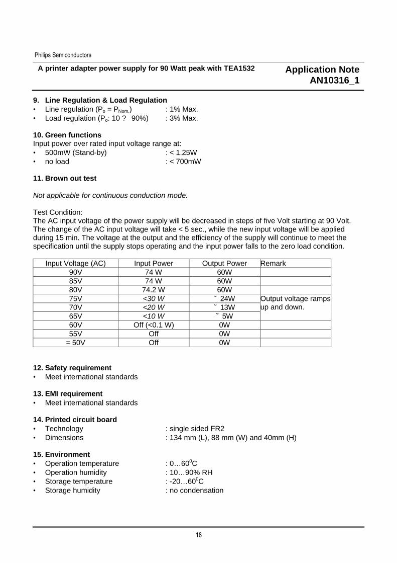
9. Line Regulation & Load Regulation • Line regulation (Po = PNom.) : 1% Max. • Load regulation (Po: 10 ? 90%) : 3% Max. 10. Green functions Input power over rated input voltage range at: • 500mW (Stand-by) : < 1.25W • no load : < 700mW 11. Brown out test Not applicable for continuous conduction mode. Test Condition: The AC input voltage of the power supply will be decreased in steps of five Volt starting at 90 Volt. The change of the AC input voltage will take < 5 sec., while the new input voltage will be applied during 15 min. The voltage at the output and the efficiency of the supply will continue to meet the specification until the supply stops operating and the input power falls to the zero load condition.
Input Voltage (AC) Input Power Output Power Remark 90V 74 W 60W 85V 74 W 60W 80V 74.2 W 60W 75V <30 W ˜ 24W 70V <20 W ˜ 13W 65V <10 W ˜ 5W
Output voltage ramps up and down.
60V Off (<0.1 W) 0W 55V Off 0W
= 50V Off 0W
12. Safety requirement • Meet international standards 13. EMI requirement • Meet international standards 14. Printed circuit board • Technology : single sided FR2 • Dimensions : 134 mm (L), 88 mm (W) and 40mm (H) 15. Environment • Operation temperature : 0…600C • Operation humidity : 10…90% RH • Storage temperature : -20…600C • Storage humidity : no condensation

A printer adapter power supply for 90 Watt peak with TEA1532
Application Note
AN10316_1
Philips Semiconductors
19
3.3 Design data The following parameters are used in the next chapters for calculation: Name Value Dim. Description VAC_min 90 V The minimum AC input voltage from the mains VAC_max 265 V The maximum AC input voltage from the mains fl_min 47 Hz The minimum line frequency fl_max 63 Hz The maximum line frequency VDC_min 77 V The minimum DC voltage across the input capacitor VDC_max 373 V The maximum DC voltage across the input capacitor VAC_nom 115 V The nominal AC input voltage for mains interruptions and lifetime
calculations Vo 20 V Output voltage Po_min 0 W Minimum output power Po_nom 60 W Nominal output power Po_max 90 W Maximum output power η > 83 % Target efficiency of the power supply at Pout = nominal Bmax 280 mT Maximum core excitation Ae 139 mm2 Effective core cross-sectional area Vf 500 mV Forward voltage drop of the secondary diode
3.4 Input and output power The output power of the circuit is 90 W peak, at a continuous output rating of 60 W. The thermal rating of the transformer has been calculated such that the peak power can be delivered during 10% of the time in 1 second intervals. The total input power of the circuit has therefore been determined to be less than 75 W, so there is no need for power factor correction.
3.5 Main supply capacitor The AC input voltage is peak rectified and buffered by a large main supply capacitor. There are two constraints determining the value of the capacitor:
o Minimum input voltage on top of the transformer: this is the peak rectified minimum AC input voltage minus the peak-peak ripple voltage;
o Nominal low input voltage interrupted during 16.7 ms The value of the input capacitor is given by the next formula in case of maximum load (75 W - “input filters” - “rectifiers” = 73 W) at minimum input voltage (90 VAC):
( ) ( )min_min_min_min_
min_
min_max_
22
2arccos
2
DCACDCACline
AC
DCo
mains VVVVf
V
VP
C+××−×××
×+×
=π
πPo_max 90 WVdc_min 77 VVac_min 90 Vf_line 50 HzC_mains 139 µF

A printer adapter power supply for 90 Watt peak with TEA1532
Application Note
AN10316_1
Philips Semiconductors
20
A simple verification can be done with respect to the mains interrupt requirement: For simplicity I assume an average current, based upon a nominal input voltage of 115 VAC at an average output power of 75 W, is drawn from the supply capacitor during one missing cycle:
A value of 150 µF is chosen.
3.6 Transformer turns ratio The two major factors here are:
o Drain to source voltage of the power switch: at the start of the demagnetization, the leakage inductance causes a voltage spike. The voltage spike due to the leakage inductance is taken here 60 Volts for the calculation.
o Reverse voltage across the secondary rectifier diode. The first factor sets a maximum to the transfer ratio, while the second factor sets a minimum.
MosFet Secondary diode STP7NB60FB PBYR20100CT
VDS-max. 540 End-of-life Vrev. 100 Vspike 60 Vforw. 0.5 Vi-max. 373 240VAC + 10% Vo 20
22.5max.
maxmaxmax =⇒
+−−
= −− NVV
VVVN
forwo
ispikeDS 66.4.min.
.max.min =⇒
−= − N
VVV
Norev
i
For the calculation, N=5 is used, but this may be changed between the above limits if the number of windings make this favorable.
3.7 Maximum duty cycle The maximum duty cycle can be calculated from the following formula: This is valid at the lowest possible supply voltage as stated in the table above. Another limitation is the maximum operating frequency of the IC. The lower maximum is 50 kHz. This gives the following result for the maximum allowed on time of the power switch:
( ) ( ) sTTTT onoscperon µδ 7.1011.12057.0max =⇒−×=−×=
N 5Vo 20 VoltVf 0.5 VoltVdc_min 77 VoltDuty 0.57
( )( ) DCFo
Fop VVVN
VVN++
+=δ
Vdc_min
Vac 115 VVdc_min 77 VPo 75 Wfrequency 60 HzCmains 168 µF
Figure 3 AC input voltage with one missing cycle

A printer adapter power supply for 90 Watt peak with TEA1532
Application Note
AN10316_1
Philips Semiconductors
21
In discontinuous operating mode, the on-time of the power switch is bound to an internal maximum of 25 µs. Since the maximum on time in normal operation is 10.7µs, this internal limit is no problem.
3.8 Transformer primary inductance The primary inductance of the transformer is determined by the requirements for minimum input voltage and maximum output power. At that operating point, the converter should run close to the maximum frequency and peak current. By designing so, the maximum power is also limited. The circuit is then switching on in the first valley after demagnetization as shown in the figure. T-on : primary stroke T-off : secondary stroke T-osc. : half cycle of the oscillation
of primary inductance and drain capacitance.
T-per. : the sum of all previous parts
V-in : supply voltage NVo : transferred secondary
voltage V-leak : voltage spike due to
leakage inductance Vds : total drain to source
voltage
The frequency of the resonant waveform after the demagnetization is determined by the primary inductance and the total capacitance present on the drain of the power switch. The frequency range of the IC for detection LVS is limited to approximately 700 kHz. Here we chose an oscillation frequency of 450 kHz, in order to reserve some headroom and limit the dV/dT of the drain voltage. The primary inductance can now be calculated according to the following formula: As a design value we choose the primary inductance 200 µH.
max
22
2 PFTV
L oni
×××
=
Vi 77 VoltTon 10.7 µsF 57 kHzPmax 98 WL 197 µH
T-on T-offT-per.
V-in
NVo Vds
V-leak
T-osc
Figure 4 Waveform on drain of power switch

A printer adapter power supply for 90 Watt peak with TEA1532
Application Note
AN10316_1
Philips Semiconductors
22
3.9 Transformer definition The peak power that has to be handled by the transformer includes the losses in the transformer and the secondary diode. The peak power is therefore increased with 5 W. The peak current in the primary loop is given by: The transformer core has been chosen a PQ26 type. The number of turns for the primary can now be calculated: The maximum magnetization of the core for the calculation has been decreased somewhat in order to create some margin at high operating temperature. The number of secondary turns then becomes:
3.10 Auxiliary winding The supply voltage of the IC has to be at least 13 Volt (max. is 20 Volt) for sufficient drive voltage of the power switch. This means that the output voltage of the auxiliary winding must be one diode voltage drop higher: 13.6 Volt. The volts per winding can be calculated from the secondary output: The auxiliary winding then must have: A number of 5 turns gives a Vcc voltage of:
93.27
5.020=⇒
+=
+= w
s
fow v
n
VVv
64.493.2
6.013min ≥⇒+
=+
≥ −aux
w
fccaux n
v
VVn
VoltVVvnV ccfwscc ⋅=⇒−×=−×= 1.146.093.25
3.10.1 dV/dt Limiter (resonance capacitor) For EMI reasons, one should limit the switch off drain-source slew voltage rate to < 8 kV / µs. The chosen resonance capacitor and the peak current in the primary winding of the transformer result in a slew rate of
3.11 Driver output and dissipation of the MOSFET The driver output of the IC has different source and sink capabilities. The maximum source current is chosen such that the power switch is turned on at a controlled rate. This causes the discharging of the drain to source capacitance in such a way that large current spikes (extreme high peak in an extreme short time) cannot occur. This helps reduce the EMI of the circuit.
L 200 µHIp 4.15 ABmax 220 mTAe 109 mm2Np 35 turns
Pmax 98 WattL 200 µHF 57 kHzIpeak 4.15 A
FLP
I p ××
= max2
e
pp AB
ILN
××
=max
7535
=⇒== ss
s nNn
n
µskVdtdV
pFC
I
dtdV
ds
p /3.7570
15.4⋅=⇒==

A printer adapter power supply for 90 Watt peak with TEA1532
Application Note
AN10316_1
Philips Semiconductors
23
The maximum sink current of the driver stage is much larger than the source capability to allow for a rapid turn-off without causing extra dissipation. The voltage slew rate must then be fixed by adding an extra capacitor across the drain-source terminals of the power switch.
3.11.1 Switching losses
The switching losses of the power switch refer to the losses due to the discharging of the capacitance that is present on the drain terminal of the device. These losses are minimized due to the valley detection of the IC. This means that the power switch will be switched on exactly at the minimum voltage of the resonant voltage swing that is present on the drain terminal. This resonance is caused by the primary inductance of the transformer and the capacitance on the drain terminal.
As can be seen in the figure, the losses are influenced by the valley where the IC switches on the power switch. The resonant voltage swing is damped somewhat which causes the amplitude to drop with each cycle. Therefore, the switching losses increase with each next cycle. The formula for the switching losses is: As one can see, the losses depend on the actual switching frequency, which again is dependent upon the output power and the input voltage. See also the application note for the TEA1507 (ref. 1). In the next table these losses are given for two input voltages and three output powers: Switching losses Input voltage Remark Output power 115 VAC 230 VAC 10 242 mW 1.33 W 60 114 mW 1.0 W 90 135 mW 0.95 – 1.12 W 230 VAC: nv = 5 or 3 The influence of the higher input voltage is of course significant: a three times higher drain voltage (“Vi – N*Vo”; where N*Vo; is attenuated more and more for a higher number of valleys nv) causes a nine times higher dissipation. Also the valley that is used to switch on the power switch influences the switching losses. In the measurements given above, at 90 W and 230 VAC, the voltage increase for the higher valley number is completely cancelled by the corresponding frequency decrease.
3.11.2 Conduction losses The conduction losses are the losses due to the RDS-on of the power switch. These losses can be calculated from the RMS current through the device:
V-in
NVo
Vds
12
34
5
Figure 5 Switching losses as a function of output valley
swDsw FVCP ×××= 2
21
onDSRMScond RIP −×= 2

A printer adapter power supply for 90 Watt peak with TEA1532
Application Note
AN10316_1
Philips Semiconductors
24
The RMS current can be calculated from the peak current using the formula: The peak current is dependant upon the input voltage and output power. However, in the case of TEA1532 there is one other point to be kept in mind: the IC uses LVS and may switch on in the first , second, third etc. valley. This means that there is more than one solution for a certain output power and input voltage combination. The peak current is given by the formula: In which nv is the number of the valley that the power switch is turned on. From the peak current, the frequency can be determined: The switching frequency must lie between the minimum and maximum limits of 31 and 65 kHz. If the frequency is outside the limits, a higher or lower valley number nv must be chosen. If we assume an average output power of 75 W with an average input voltage of 100 VDC, it can be found that with nv = 2, the peak current is 3.6 Ampere with an operating frequency of 56 kHz. The RMS current becomes 1.34 Ampere. This results in conduction losses of 4.3 W (Tj = 125 °C and Rds-on = 1.2 O max at 25 °C)
3.11.3 Total losses The sum of switching and conduction losses is the total power dissipation of the power switch. The maximum power dissipation is 4.5 W at minimum input voltage and maximum output power.
3.12 Current sense resistor When the peak current is known, the value of the current sense resistor can be calculated. From the transformer calculations, a peak current of 4.15 Ampere was determined. This gives a current sense resistor of: Because the sense voltage of the IC has some tolerance (+/- 8%) and there is some headroom necessary, the actual value for the resistor is decreased with 20%. Furthermore, to lower the total inductance of this measuring resistor, three devices are connected in parallel: Rcs = 0.39 Ω // 0.39 Ω // 0.22 Ω. All resistors should be types with low inductance. The power dissipation is worst case is when the peak current is reached with the highest duty cycle:
3.13 Soft-start circuit The soft start circuit is established by means of a reduced peak current during start up. The reduced peak current is realized by means of a decreasing voltage source between current sense resistor and current sense input of the IC.
3δ
peakRMS II =
( )1222
−+
++
+= v
P
D
io
io
io
iopeak n
LC
PPVNVVNV
PVNVVNV
I π
( )1
12−
−+
+= DPv
io
ioP CLn
VNVVNV
LIF π
mWPRrmsV
Pcscs R
cs
csR ⋅=⇒
×== 500
103.0
)357.0
52.0()(2
2
Ω⋅=== 125.015.452.0
p
cscs I
VR

A printer adapter power supply for 90 Watt peak with TEA1532
Application Note
AN10316_1
Philips Semiconductors
25
For soft-start, the RC components R113 and C111 are calculated as follows: • with the soft start current, the voltage drop across the resistor must be larger than the over current
protection level of 520 mV:
Ω⋅==≥ 86666052.
113 µIV
RSS
CS Take R113 =12 kΩ.
• the soft start timing is determined by R113 x C111; This time should be chosen short enough to avoid the activation of the protection pin. During the start up, the protection pin sources a current due to the fact that the control voltage is still below the limit of 630 mV (Control detect level). This means that in this application the soft start time should be below 40 ms ( see chapter 2.6.10 for the protection timing calculations):
FCR
C µτ
⋅<⇒=< 3.312000
04.0111
113111
To enable a rapid start up, we choose C111 = 220nF: this will cause a short start up time of less than 3 ms. NB: the soft start circuit time has nothing to do with the start up of the Vcc. The VCC is first charged up to the start level, then the IC initiates the soft start timing.
3.14 Peak clamp The peak clamp circuit consists of D105, C106 and R104 optionally an additional R103. Since the power switch is a 600 Volt device, the diode must have the same voltage specification. The peak current rating must exceed the peak current in the primary of the transformer: 4.4 A. The average current however is much smaller. Important is also the switching behavior: the diode should have very low forward recovery voltage and low reverse recovery time. The voltage across C106 is assumed to be constant, under the condition: The dissipation of R104 can be calculated using: As a rule of thumb the dissipation level in a resistor should be half its rated value. For a 500 mW resistor, this results in: The voltage across the power switch after switch off equals: This is higher than Vin-dc so the diode will conduct and the voltage UR across the resistor R104 equals the voltage difference: leading to: Solving for R104 results in: Given the initial boundary condition:
switchfCR
1106104 >>⋅
104
2
RV
P RR =
WPR 25.0=
leakagespikeodcinoffDS VNVVV ___ ++=
leakagespikeoR VNVV _+=
( )25.0
2_ =
+=
R
VNVP leakagespikeo
R
( ) ( )Ω=
+⋅=
+= k
P
VNVR
R
leakagespikeo 10025.0
60205 22_
104
min_106104
1
switchfCR >>⋅=τ

A printer adapter power supply for 90 Watt peak with TEA1532
Application Note
AN10316_1
Philips Semiconductors
26
The capacitor value can be found:
pFRf
Cswitch
323101001031
1133
104min_106 >>
⋅⋅⋅>>
⋅>>
The capacitor however is in first instance charged by the peak current of the primary winding of the transformer. This causes momentarily a large increase of the voltage that must be limited in order to meet the maximum voltage limitation of the power switch. Therefore the value of C106 is taken 10 nF. The voltage rating is 200 Volt. The diode D8 should be a fast type to effectively clamp the voltage spike of the leakage inductance. The reverse voltage rating of diode D8 should be the same as the maximum voltage rating of the power switch. The minimum reverse voltage rating is therefore 650 V. The peak forward current can be equal to the peak current in the transformer primary (and this is a repetitive current), i.e. 4.15 A. The average current is however rather low, Iav < 1 A.
3.15 Demag sensing The demag sensing is a simple resistor tied between pin 5 and the VCC winding. This value of this resistor however is determined by the brown out protection function, which will be discussed next.
3.16 Brown out protection The brown out protection can be calculated by the following formula:
threshold
DCi
p
aux
threshold
cc
I
V
nn
IV
R _122 ×==
n_aux 5 turnsn_prim. 35 turnsVdc_min 80 VIthr. 66 µAR122 173 kΩ
The minimum input voltage limit must be chosen below the lowest ripple voltage at minimum AC input. In other words, if the minimum operating voltage, as measured on the mains smoothing capacitor C105, under peak load conditions, is 80 Volt, then the value of R122 must be less than 173 kΩ. We choose R122 = 150 kΩ, which sets the value for the minimum supply voltage to 63 +/- 6.3 Volt (excluding tolerances in the transformer and the resistor).
3.17 Over temperature protection The over temperature protection is realized with an external NTC resistor R105. This NTC is thermally connected to the heatsink of the power switch. The temperature sensing circuit has a built in threshold D108 and D109, to decouple it from the rest of the protection circuit. A 6.2 Volt zenerdiode is chosen for it’s excellent performance: low leakage current, sharp zenering behaviour and low temperature dependancy. The total threshold is now: VoltVVVVvV ththotectDDth ⋅=⇒++=⇒++= 1.95.24.02.6Pr109108 The resistance of the NTC with respect to temperature is given in the datasheet of the device. From these data it can be derived that with the threshold of 9.1 Volt, a supply voltage of 12.4 Volt, resistor R106 should be 6200 O for a protection level of 140 °C.

A printer adapter power supply for 90 Watt peak with TEA1532
Application Note
AN10316_1
Philips Semiconductors
27
3.18 Over voltage protection The overvoltage protection uses the auxiliary winding to detect an overvoltage. The winding voltage is attenuated (R118 / R119) and the leakage inductance spikes are filtered out of the signal to prevent false triggering (C112). The output is rectified (D111) and smoothed with the already present timing capacitor (C109). The presence of R108 is to add a small discharge current to prevent charging of C109 due to increased leakage current of D111 at high temperatures. Capacitive feedthrough by D111 is reduced by means of resistor R109. This protection however functions only well if the auxiliary and the secondary winding are well coupled. The OVP level can be determined with the following formula:
( ).Pr111_119
119118secotDF
aux
VVR
RRNN
OVP +×+
×=
n_sec 7 turnsn_aux 5 turnsR_118 13 kΩR_119 2.7 kΩVf_D111 0.5 VV_prot 2.5 V
OVP 24.4 V
3.19 VCC supply The windings in this transformer design are such that the coupling between the auxiliary winding and the secondary winding is quite low. This results in a large voltage spike on the auxiliary winding and that causes a large variation in winding output voltage with respect to the secondary load. This variation is such that the maximum voltage on the IC pin 1 is exceeded. The VCC supply is therefore equipped with a series stabilizer to prevent too high voltages on pin 1 of the IC.The extra series stabilizer consists of Q102 / D110 / R107 and supplies a constant voltage of 12.4 V to the IC. Capacitor C108 is the buffer for the start up current. Capacitor C113 must have a high voltage rating due to the peak rectification. This can give an output voltage of upt 37 Volt depending upon the coupling of primary and secondary winding and the output power.
3.20 Secondary diode The design of the transformer regarding the turns ratio is such that the maximum reverse voltage for D201 is limited to 100 Volt. This means that we can use a Schottky barrier type, which gives low forward voltage drop and subsequent low power dissipation. The peak current in the diode is:
.201ˆˆ
prims
pD I
n
nI ×=
The RMS current is then:
3ˆ)( 201201
δ×= DD IRMSI
And an average current of:
2
ˆ)( 201
201
δ×= D
D
IAVI
np 35 turnsns 7 turnsIprim. 4.15 AI(D201) 20.75 A
duty 0.4I(RMS) 7.58 A
I(AV) 4.15 A

A printer adapter power supply for 90 Watt peak with TEA1532
Application Note
AN10316_1
Philips Semiconductors
28
The parallel connection of the two diodes of one PBYR20100 is adequate for the application, both in reverse voltage and forward current. From the datasheet, we find the equivalent series resistance of the diode is 11 mΩ (at 125 °C) and a forward voltage drop of 0.63 Volt; leakage current at this temperature is < 150 µA. The power dissipation therefore is:
δ××+×+×= RRRMSavFD IVRIIVP 2201
Vf 0.63 VIav 4.15 AIrms 7.58 AR 0.011 ΩVr 100Ir 150 µAduty 0.4P 3.25 W
The high power dissipation of the diode makes it necessary to mount the diode on a heatsink.
3.21 Secondary capacitor The value of the secondary capacitor(s) is mainly determined by the ripple current, the voltage rating must comply with the maximum value in case of an error situation (open feedback loop). The ripple current is determined for an average output power of 75 W:
According to the data sheet, 2 capacitors in parallel of 1000 µF from the ZL series of Rubycon are allowed up to 2.5 Ampere each at 105 °C. Therefore, caution should be taken when using the design at maximum load during longer periods of time and/or at higher ambient temperature.
3.22 Voltage feedback circuit The voltage feedback circuit is kept very simple but nevertheless achieves high accuracy. No adjustment is available nor necessary, therefore the value of the output voltage can vary 2 – 3 % from sample to sample. The inclusion of the TL431 in the feedback loop however certifies good stability and high ripple and load rejection.
3.22.1 Error amplifier The output voltage division with R204 and R205 exactly matches the requirement for a 20 Volt output. In standby conditions (no load) the resistors also form a minimum load of 40 mW. This minimum load assures the continued operation of the circuit under no load conditions without performing restarts. The values for the feedback around the TL431 (R203 / C203 / C204) are determined in the actual working circuit by means of a network analyzer. These values depend on a large number of factors due to the fact that the gain of the circuit varies with load. For details on designing this part of the circuit, the author wishes to refer to the existing literature on this part.
Vin_DC 100 200 300 373 VF 56210 64400 59114 61492 HzIp_prim 3.62 3.38 3.53 3.46 AN 5 5 5 5Ip_sec 18.1 16.9 17.65 17.3 Aduty(sec) 0.41 0.44 0.42 0.43Ic_RMS 5.66 5.39 5.56 5.48 A
134
__ −=δDCORMSC II

A printer adapter power supply for 90 Watt peak with TEA1532
Application Note
AN10316_1
Philips Semiconductors
29
3.22.2 Opto-coupler The LED of the opto-coupler is directly fed from the output voltage since this is the only available source on the secondary side. An extra low pass filter to remove disturbing components from this supply is not necessary. The value of R201 is chosen such that at higher frequencies, where the TL431 acts as a voltage source, the loop transfer is already low enough without disturbing the stability. The transistor of the opto-coupler is connected to the supply via a resistor R121. In case of a short circuit of the collector to emitter of the opto-coupler transistor, this resistor prevents the voltage on the control pin 4 from reaching too high (damaging) values. If necessary, in case of large ripple voltages on the supply, capacitor C114 can be added to reduce feedthrough of especially high frequency spikes.
3.22.3 Loop response The loop response was measured using a network analyzer. The result is a bandwidth of 4.2 kHz and a phase margin of 58 degrees at 60 Watt load and 230VAC.
3.23 Miscellaneous A printed circuit board was designed with the circuit as shown in Error! Reference source not found.. A complete sample board can be requested from the sales department. For a new design, some points should be kept in mind for the layout:
o Mains input part: keep input tracks close together to reduce possible pick-up. o Primary current loop: keep area as small as possible to minimize stray field. o Secondary current loop: keep area as small as possible to minimize stray field. o Feedback sensing point: connect the sensing points of the erorr amplifier part to the output
connector directly. This will compensate for possible voltage drop of copper tracks. o Current sense input: place a resistor in series with the soft start RC combination to prevent
charging of the soft start capacitor during normal operation. This causes an offset voltage that effectively reduces the peak current and the maximum output power. See also reference 1.

A printer adapter power supply for 90 Watt peak with TEA1532
Application Note
AN10316_1
Philips Semiconductors
30
3.24 Complete circuit diagram
Figure 6 Circuit diagram for discontinuous conduction mode

A printer adapter power supply for 90 Watt peak with TEA1532
Application Note
AN10316_1
Philips Semiconductors
31
4. DESIGN OF AN ADAPTER SUPPLY FOR GLOBAL MAINS IN CCM
4.1 Introduction to design This chapter shows a way of design of an adapter power supply operating in the continuous conduction mode. As in the previous chapter, all critical components will be treated and measurement results will be given. Since the specification is the same, reference is made to chapter 3.2. The same holds for the design data, see chapter 3.3.
4.2 Transformer turns ratio The maximum turns ratio of the transformer is limited by the maximum voltage of the power switch. On the lower side, the reverse voltage of the secondary diode is limiting the turns ratio of the transformer. One other point the designer has to keep in mind is the minimum output power in continuous conduction mode: when the load drops, the current in the transformer will also decrease and at a certain load the current will not be continuous anymore and the converter changes to discontinuous conduction mode. A fair design criterion is to choose the lower continuous conduction power output around ¼ to ½ of the maximum output power. A lower minimum value increases the primary inductance that increases the core size. In this design the following start values have been chosen:
The reverse voltage for the secondary diode has been increased to 150 Volt to allow a smaller turns ratio that is beneficial for the switching losses. Otherwise the primary inductance increases significantly (resulting in a large core size) or the lower limit of continuous conduction operation increases to an unacceptable value. Given above data, the turns ratio must be between 2.87 and 5.17. For this design is chosen for N = 3.
4.3 Maximum duty cycle In this application, the duty cycle is given by the range of the input voltage (fixed turns ratio):
Oi
O
VNVVN×+
×=δ
N 3Vo 20.6 VoltVi_min 77 Volt Vi_max 373 Voltduty_max 0.45 duty_min 0.14
The maximum duty cycle of the IC is 70 %. Therefore there is no conflict with the IC limit.
373 V maximum bridge voltage80 V minimum bridge voltage
20.0 V nominal output voltage37.0 W minimum output power for CCM90.0 W maximum output power540 V breakdown voltage MOSFet excl. leakage spike; end of life150 V reverse voltage sec. diode63 kHz fixed switching frequency TEA1532 data
Global mains range minus capacitor ripple voltage

A printer adapter power supply for 90 Watt peak with TEA1532
Application Note
AN10316_1
Philips Semiconductors
32
4.4 Primary peak current The primary peak current is defined now and can be calculated using the following formula:
p
DC
DC
oP LF
V
V
PI
××
×+
×=
2maxmin_
maxmin_
max_ δ
δ
)
Po_max 90 WVdc_min 77 VDuty max 0.446F 63 kHzLp 682 µHIpeak 3.02 A
4.5 Transformer definition The primary inductance can now be calculated from the minimum CCM power (= 37 W) at maximum AC input voltage:
FI
NVL
out
inp ××
××=
min_
minmax_
2
δ
Vi_max 373 VN 3Duty_min 0.14Iout_min 1.85 AFreq. 63 kHzLp 682 µH
The core for this design was chosen a PQ type. The PQ26 core, as used in the design in discontinuous conduction mode, cannot be used due to insufficient winding space with the desired inductance. Therefore a one size bigger core, the PQ32 is used. The turns ratio was chosen as stated above due to the available winding area and preference for triple insulated wire for this sample transformer. This gives the following winding data:
e
ppp AB
ILn
×
×=
max
ˆ
Lp 682 µHIp 3.02 ABmax 280 mTAe 169 mm2np 43.5 turns
With 42 turns of primary windings, the winding fits on two layers. This will increase the magnetization somewhat, but this is not such a big problem due to the continuous conduction mode that uses only a small modulation range of the magnetization. For a turns ratio N = 3, the secondary winding then becomes 14 turns. The current amplitudes are shown in the next table: Item value Formula Remark Primary peak current 3.02 A See above Primary start current 2.22 A
FLV
IIP
iPStartP
δ×−= min_
_
)
Secondary start current 9.05 A PS INI
))×=
Secondary end current 6.73 A
FLV
IIS
outSEndS
δ−−=
1_
)
Output power is 90 Watt, which may drive the core close to saturation.

A printer adapter power supply for 90 Watt peak with TEA1532
Application Note
AN10316_1
Philips Semiconductors
33
4.6 Auxiliary winding With reference to chapter 3.10: 47.1
146.020
=⇒+
=+
= ws
fow v
n
VVv
The auxiliary winding then must have: 25.9
47.16.013min ≥⇒
+=
+≥ −
auxw
fccaux n
v
VVn
A number of 10 turns gives a Vcc voltage of: VoltVVvnV ccfwscc ⋅=⇒−×=−×= 1.146.047.110
4.7 Power switch
4.7.1 Switching losses The power switch is in continuous conduction mode hard switching. This means that for the switching losses, the most unfavorable situation: maximum drain voltage; must be used. Since the frequency is fixed at 65 kHz, the switching losses are maximal at the highest input voltage.
4.7.2 Conduction losses The conduction losses depend upon the current through the device and therefore upon the output power. The losses are maximal during maximum load, however for this calculation I assume an average load of 75 W. The current in the power switch is:
SWPoi
oi
oi
oiEndStart FLNVV
NVVNVVNVV
PI2
1/_ ++−
+×=
For IStart take “-“ and for IEnd take “+” in the calculation. The RMS value of this waveform is: ( )
322 δEndEndStartStartRMS IIIII ++=
I_start
I_end
0d
With an average power of 75 W the result is as stated in the next table: Lp 682 µH Fsw 63 kHz N 3 Vout 20.6 VPout 75 W Rds(25) 1.2 Ω Rds(125) 2.41 ΩVdc 100 V Vdc 200 V Vdc 300 V Vdc 373 Vduty 0.38 duty 0.24 duty 0.17 duty 0.14Istart 1.52 A Istart 1.04 A Istart 0.87 A Istart 0.80 AIend 2.41 A Iend 2.14 A Iend 2.06 A Iend 2.03 AIrms 1.22 A Irms 0.79 A Irms 0.62 A Irms 0.55 AP(25) 1.80 W P(25) 0.74 W P(25) 0.46 W P(25) 0.36 WP(125) 3.61 W P(125) 1.49 W P(125) 0.93 W P(125) 0.73 W The conduction losses decrease with increasing input voltage. The losses are maximal with minimum input voltage and maximum output power.
swDsw FVCP ×××= 2
21
Cd 570 pF N 3 Vo 20.6 V F 63 kHzVdc 100 V Vdc 200 V Vdc 300 V Vdc 373 VPsw 0.5 W Psw 1.2 W Psw 2.4 W Psw 3.4 W

A printer adapter power supply for 90 Watt peak with TEA1532
Application Note
AN10316_1
Philips Semiconductors
34
4.7.3 Total losses The total losses can be retrieved from the sum of switching and conduction losses. Since the switching losses are maximal when the conduction losses are minimum and vice versa, the result is the same at minimum and maximum input voltage. The maximum power dissipation by the power switch is therefore 4.1 W. The heatsink has been chosen for this power dissipation.
4.8 Current sense resistor The current sense resistor is defined by the formula: Ω⋅=== 172.0
02.352.0
p
cscs I
VR
The actual resistor is corrected for tolerances. A combination of three resistors in parallel has been chosen: Rcs = 0.39 Ω // 0.39 Ω // 0.68 Ω The worst case is when the peak current is reached with the highest duty cycle:
mWPRrmsV
Pcscs R
cs
csR ⋅=⇒
×== 267
152.0
)345.0
52.0()(2
2
All resistors should be types with low inductance.
4.9 Over voltage protection The OVP level can be determined with the following formula:
( ).Pr111_119
119118secotDF
aux
VVR
RRNN
OVP +×+
×=
n_sec 14 turnsn_aux 10 turnsR_118 13 kΩR_119 2.7 kΩVf_D111 0.5 VV_prot 2.5 V
OVP 24.4 V
4.10 Vcc supply The voltage spike on the auxiliary winding is quite low due to a very good coupling of primary and secondary winding and also between auxiliary and secondary winding. Therefore the supply voltage variation on pin 1 with respect to the load variation of the secondary output is quite low. This means that there is no extra series stabilizer necessary.
4.11 Secondary diode The secondary diode must not only be able to handle the secondary current and the applicable reverse voltage, but a further requirement is fast switching: the power switch is turned on while the secondary diode is still conducting. Fast reverse recovery is therefore of utmost importance. During this reverse recovery time, the primary current is only restricted by the leakage inductance of the transformer. Carefully choosing the secondary diode type is therefore important. The average current in the diode can be determined from the average output power. With an average output power of 75 W and a forward voltage drop of 600 mV, the average power dissipation of the diode is 2.25 W.

A printer adapter power supply for 90 Watt peak with TEA1532
Application Note
AN10316_1
Philips Semiconductors
35
4.12 Secondary capacitors The ripple current in the capacitors is given by the following formula:
( ) 222_ 3
1AVEndEndStStRMSC IIIIII δ
δ++×+
−=
I_start
I_end0
dI_out
In the next table, the current in the capacitors is calculated at four different input voltages: Lp 682 µH Fsw 63 kHz N 3 Vout 20 VPout 77.6 W Vf 0.7 VVdc 100 V Vdc 200 V Vdc 300 V Vdc 373 Vduty(pr) 0.38 duty(pr) 0.24 duty(pr) 0.17 duty(pr) 0.14Istart 7.41 A Istart 6.57 A Istart 6.32 A Istart 6.23 AIend 4.74 A Iend 3.26 A Iend 2.73 A Iend 2.51 AIav 3.75 A Iav 3.75 A Iav 3.75 A Iav 3.75 AI_RMS 3.02 A I_RMS 2.25 A I_RMS 1.95 A I_RMS 1.82 A
Output capacitor current
With two capacitors of 1000 µF in parallel, each having a ripple current rating of 2.36 A, the above calculated values are well within limits.
4.13 Loop response It is well known that a continuous conduction mode converter may become unstable with duty cycles exceeding 50%. Even at 30 % duty cycle, the so-called high-low mode may be observed: the duty cycle switches between a shorter and a longer one every two cycles. To overcome this problem, slope compensation is added to make the loop stable again. Adding slope compensation is made easy with the TEA1532: only one extra resistor is necessary. In the circuit diagram on page 37, this is R125. The IC sources a current out of pin 4 with an amplitude of 1 µA / µs; starting each cycle again at zero. This means that the control voltage increases with an amplitude that can be set by the value of R125. The increasing voltage on the control pin means a decreasing peak current in the primary of the transformer which stabilizes the control loop. The following formula is well known from the theory about slope compensation for continuous conduction mode:
2
UpDownSC
KKK
−=
The above slopes are defined by:
SCSCSC
CSP
InUp
CSP
OutDown
RIK
RLV
K
RL
NVK
=
=
=
ISC is a sawtooth shaped current! Filling last three definitions in the first equation and solving for the slope compensation resistor:

A printer adapter power supply for 90 Watt peak with TEA1532
Application Note
AN10316_1
Philips Semiconductors
36
( )SCP
CSinoutSC IL
RVNVR
2−=
Vout 20.6 VVin 150 VRcs 0.15 ΩLp 682 µHIsc 1 µA/µsRsc 10 kΩ
PS: In this design I have chosen for a minimum duty cycle of 30 % to start the slope compensation. The 30 % duty cycle resembles an input voltage of 150 VDC. In practice a value of 11 kΩ is working fine.

A printer adapter power supply for 90 Watt peak with TEA1532
Application Note
AN10316_1
Philips Semiconductors
37
4.14 Complete circuit diagram
Figure 7 Circuit diagram for continuous conduction mode

A printer adapter power supply for 90 Watt peak with TEA1532
Application Note
AN10316_1
Philips Semiconductors
38
5. MEASUREMENTS
5.1 Discontinuous conduction mode The following measurements were done in a sample demo board as they are available.
5.1.1 Start up 115 VAC 230 VAC
Ch. 1: Vcc Ch. 2: Vout Ch. 3: Main supply capacitor C105 Ch. 4: Aux supply capacitor C113 Output load is 60 Watt
5.1.2 Ripple rejection 115 VAC 230 VAC
Ch. 2: Vout Ch. 3: Main supply capacitor C105 Output load is 60 Watt

A printer adapter power supply for 90 Watt peak with TEA1532
Application Note
AN10316_1
Philips Semiconductors
39
5.1.3 Pulse load 115 VAC 230 VAC
Ch. 1: Iout Ch. 2: Vout
5.1.4 Drain voltage and current 115 VAC 230 VAC
Ch. 3: Drain voltage Ch. 4: Drain current as measured across the sense resistor Output load is 60 Watt

A printer adapter power supply for 90 Watt peak with TEA1532
Application Note
AN10316_1
Philips Semiconductors
40
5.1.5 Output short circuit 115 VAC 230 VAC
Ch. 3: Drain voltage Ch. 4: Drain current as measured across the sense resistor
5.1.6 Efficiency
Output load 115 VAC 230 VAC No load 250 mW 385 mW 60 W 71.6 W 83.8 % 71.5 W 83.9 % 90 W 108.7 82.8 % 105.1 85.6 %
5.2 Continuous conduction mode The following measurements were done in a sample demo board as they are available.
5.2.1 Start up 115 VAC 230 VAC
Ch. 1: Vcc Ch. 2: Vout Ch. 3: Main supply capacitor C105 Output load is 60 Watt

A printer adapter power supply for 90 Watt peak with TEA1532
Application Note
AN10316_1
Philips Semiconductors
41
5.2.2 Ripple rejection 115 VAC 230 VAC
Ch. 2: Vout Ch. 3: Main supply capacitor C105 Output load is 60 Watt
5.2.3 Pulse load 115 VAC 230 VAC
Ch. 1: Iout Ch. 2: Vout

A printer adapter power supply for 90 Watt peak with TEA1532
Application Note
AN10316_1
Philips Semiconductors
42
5.2.4 Drain voltage and current 115 VAC 230 VAC
Ch. 3: Drain voltage Ch. 4: Drain current as measured across the sense resistor Output load is 60 Watt
5.2.5 Output short circuit 115 VAC 230 VAC
Ch. 3: Drain voltage Ch. 4: Drain current as measured across the sense resistor

A printer adapter power supply for 90 Watt peak with TEA1532
Application Note
AN10316_1
Philips Semiconductors
43
Ch. 1: Control pin 4 voltage Ch. 2: Vcc pin 1 supply line Ch. 3: Drain voltage Ch. 4: Protect pin 3 voltage The picture on the left hand shows the moment of short circuiting the output: The feedback voltage immediately drops to zero volt; The protect pin voltage is at 2 Volt due to the OVP circuit and starts to increases smoothly. This increase is due to the current sourced by the protect pin, charging the capacitor C109. When the protect pin voltage hits the 2.5 V level, the protect is activated an a safe-restart sequence is initiated. The picture on the right hand side slows the respective voltages at a continued short circuit. Mind the different time scales for both pictures!
5.2.6 Efficiency
Output load 115 VAC 230 VAC No load 190 mW 230 mW 60 W 69.9 W 85.8 % 67.9 W 88.4 % 90 W 108.1 W 83.3 % 102.3 W 88.0 %

A printer adapter power supply for 90 Watt peak with TEA1532
Application Note
AN10316_1
Philips Semiconductors
44
6. FAULT FINDING TREE
6.1
Mai
n tr
ee
Start
Mains NOTconnected
Visual check oforientation ofdiodes andcapacitors
Check D201, C201and C202
Connect themains
supply (115/ 230 VAC).
19.5V< Uout <20.5V?
no
Connect 3A DCload to output.
Connect dynamicload to output:
3.0A: duty = 90%4.5A: duty = 10%
F = 100 Hz
Output ripple< 100mVpp ?
Disconnect allloads.
Input power< 1 Watt?
yes
yes
yes
Supply oké
no
no
yes
19.5V< Uout <20.5V?
no
Check feedbackloop.Check output part.
Measureimpedance on
outputconnector:
>100Ω
no
Connect outputload of 1 A.
Input power:70 W<Pi<80 W
Check MosFetpart.
no
yes
Check Vcc part.
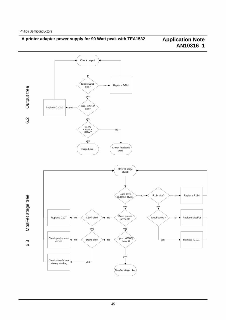
A printer adapter power supply for 90 Watt peak with TEA1532
Application Note
AN10316_1
Philips Semiconductors
45
6.2
Out
put t
ree
Diode D201oke? Replace D201
Replace C201/2Cap. C201/2
oke?
yes
yes
Check output.
19.5V< Uout <20.5V?
yes
yes
no
Output oke. Check feedbackpart.
no
6.3
Mos
Fet
sta
ge tr
ee Gate drive
pulses > 8Vp? R114 oke? Replace R114
Replace C107 Drain pulsespresent?
Check transformerprimary winding.
yes
yes
no
yes
no
MosFet stagecheck
Up = U(C105)+ Nvout?
C107 oke?
D105 oke?
yes
no
no
yes
Check peak clampcircuit.
no
no
yes
Replace IC101.
MosFet oke?
MosFet stage oke.
no
yes
Replace MosFet

A printer adapter power supply for 90 Watt peak with TEA1532
Application Note
AN10316_1
Philips Semiconductors
46
6.4
Vcc
tree
11.5 V< Vcc < 15 V?
Vcc: sawtoothwaveform?
Check C108,C113, D112,
D110, Q102, R107and R120.
Check R111.Drain voltage> 90 Volt DC?
Check F101, L101,D101/2/3/4, and
R102.
yes
yes
no
yes
no
Check Vcc Pin 1.
Protect pin 3:U < 2.3 V?
Voltage onC105 > 90 V
DC?
Mains voltage> 90 V AC?
no
yes
Check cathodeD108:
U < 8 V?no
yes
Increase mainsvoltage.
no
no
yes
Replace resistor.
yes
Gate pulses pin7 present?
R112 - R117oke?
no
Check MosFetpart.
Uctrl pin 4< 1.5 V?
Vcc oke.
no
yes
Replace IC101.
yes
Check feedbackpart.
no

A printer adapter power supply for 90 Watt peak with TEA1532
Application Note
AN10316_1
Philips Semiconductors
47
6.5
Fee
dbac
k lo
op tr
ee
Check ref. PinIC201: 2.5 V Check R204/5
Check C108,C113, D112,
D110, Q102, R107and R120.
Replace R201CathodeIC201:
3V<U<18V?
Check R121,C114.
correct
yes
no
yes
no
Feedback loop.
IC101 pin 4:0.9<U<1.5V?
R201 oke?
Opto-coupleroke?
no
yes
Check cathodeD108:
U < 8 V?no
yes
Replace opto-coupler. no
no
correct
Replace R201.yes
Check C204
R201 oke no
Ripple oke?
Feedback oke.
no
yes
Replace IC101.
yes
noCheck C110,
R110, C203 andR203.
Opto-couplersupply oke?
Check C110,R110.

A printer adapter power supply for 90 Watt peak with TEA1532
Application Note
AN10316_1
Philips Semiconductors
48
7. REFERENCES 1. 75 W SMPS with TEA1507 Quasi-Resonant Flyback Controller AN00047 2. A 45 Watt adapter power supply AN1033

A printer adapter power supply for 90 Watt peak with TEA1532
Application Note
AN10316_1
Philips Semiconductors
49
8. APPENDIX 1: BROWN OUT IN CONTINUOUS CONDUCTION MODE. In continuous conduction mode, the demagnetization sensing pin 5 is short circuited to ground normally. This not only disables the demagnetization sensing, but also the brown out protection circuit. However, with a trick, the brown out protection can be used in the continuous conduction mode as well. The circuit diagram below shows part of the CCM application circuit (see Figure 7) but with the additional parts for the realization of the brown out protection:
Figure 8 Circuit diagram for continuous conduction mode with additional brown out circuit
Explanation of brown out circuit: D113: To rectify the AC waveform in order to use only the negative part which is a measure for
the input voltage. R120: Any leakage current from D113 is led to ground otherwise C113 would be charged
positive which would bias the input. R121: This resistor determines the actual brown-out point/voltage. R122: Due to the high value of R121, this resistor is necessary to fix the voltage on the demag
pin 5 at 0 Volt during the positive part of the waveform. C113: Acts as a leading edge blanking: the first part of the negative part of the waveform shows
some ringing that must be filtered out to prevent false triggering. Design rules for the component ratings and values:
D113 The reverse voltage rating of this diode equals the positive part of the waveform; therefore the rating equals the Vcc voltage of the IC; a 20 Volt device should be sufficient. The current rating is < 10 mA.
R120 A more or less fixed value; to be determined in the actual application, but 18 kΩ is a good starting value.
R121 Vi_min The minimum input voltage that must be detected.

A printer adapter power supply for 90 Watt peak with TEA1532
Application Note
AN10316_1
Philips Semiconductors
50
N_aux Number of windings of the auxiliary or Vcc winding.
N_p Number of primary windings. V(D113) Forward voltage drop of the diode at a
current of 60 µA. Vneg-clamp
Negative clamping voltage of the demag input pin 5 of the TEA1532: typical 450 mV.
122
113min_
121
RV
I
VVnn
VR
clampnegoutBrown
clampnegDp
auxi
−−
−
+
−−×≤
I(brown-out)
Brown-out current specification of the demag input pin 5 of the TEA1532: typical 60 µA.
R122 Should not be chosen larger to prevent false “magnetization” sensing! A lower value will further decrease the value of R121. This can be less favorable for the efficiency during stand-by.
C113 The time constant R122//R121 x C113 should be chosen approximately 1.5 µs. However this depends strongly on the transformer used in the application (ringing period).


