IEEE TRANSACTIONS ON CIRCUITS AND SYSTEMS FOR VIDEO TECHNOLOGY, VOL. 21, NO. 2, FEBRUARY 2011 101 A Priority-Based 6T/8T Hybrid SRAM Architecture for Aggressive Voltage Scaling in Video Applications Ik Joon Chang, Debabrata Mohapatra, and Kaushik Roy, Fellow, IEEE Abstract —We present a voltage-scalable and process-variation resilient, hybrid memory architecture, suitable for use in MPEG- 4 video processors such that power dissipation can be traded for graceful degradation in “quality.” The key innovation in our proposed work is a hybrid memory array, which is a mixture of conventional 6T and 8T SRAM bit-cells. The fundamental premise of our approach lies in the fact that the human visual system is mostly sensitive to higher order bits of luminance pixels in video data. We implemented a preferential storage policy in which the higher order luma bits are stored in robust 8T bit- cells while the lower order bits are stored in conventional 6T bit-cells. This facilitates aggressive scaling of supply voltage in memory as the important luma bits, stored in 8T bit-cells, remain relatively unaffected by voltage scaling. The not-so-important lower order luma bits, stored in 6T bit-cells, if affected, contribute insignificantly to the overall degradation in output video quality. Simulation results show that under iso-area condition, we can obtain at least 32% power savings in the hybrid memory array compared to the conventional 6T SRAM array. Index Terms—Aggressive voltage scaling in SRAM, hybrid SRAM array, low power SRAM design, process variation resilient SRAM, video memory. I. Introduction T HE WIDESPREAD availability of 3G communication networks, coupled with the growing popularity of power- ful smart-phones, has fueled the exponential growth of demand for multimedia services in wireless communications. As more and more functionality is integrated into hand-held mobile devices such as cell phones and personal digital assistants, the corresponding power dissipation associated with these devices is increasing as well. Hence, it is of paramount impor- tance for mobile devices supporting multimedia applications to provide lower power dissipation to prolong the battery life of these devices. The Moving Pictures Experts Group (MPEG-4) audio visual standard [1] has been instrumental in bringing several multimedia applications (primarily video) to Manuscript received July 8, 2009; revised November 16, 2009 and May 19, 2010; accepted July 6, 2010. Date of publication January 13, 2011; date of current version March 2, 2011. This work was supported by Semiconductor Research Corporation and the Focused Center Research Program—Gigascale Systems Research Center. This paper was presented in part at the Design Automation Conference, 2009. This paper was recommended by Associate Editor S.-Y. Chien. The authors are with Purdue University, West Lafayette, IN 47907 USA (e-mail: [email protected]; [email protected]; [email protected]). Color versions of one or more of the figures in this paper are available online at http://ieeexplore.ieee.org. Digital Object Identifier 10.1109/TCSVT.2011.2105550 the mobile devices and is the current de-facto standard for wireless multimedia communications. Due to its widespread prevalence, it forms the basis of our motivation to investigate low power techniques for MPEG-4 hardware. The primary source of power dissipation in MPEG-4 video processors is memory access power [2]. In previous literature [2], re- searchers have employed algorithm level techniques to reduce the memory access power. In digital circuits, switching power dissipation is expressed as “αCV DD 2 f” (α: activity factor, C: effective capacitance, V DD : supply voltage, and f: operating frequency) [3]. The algorithm level techniques mainly decrease the number of basic arithmetic operations per second and/or the number of memory accesses by data reuse. In the other words, the switching power is improved by reducing α and f for the memory accesses. Due to the quadratic dependence of switching power dissi- pation on V DD , we can also lower power by supply voltage scaling. Unfortunately, failure probability of conventional 6T SRAM bit-cell increases considerably as the supply voltage is scaled down [4], imposing a lower bound on the supply voltage. It should be noted that read failure, which occurs due to lack of read static noise margin (SNM) [8], is one of the major failures impeding supply scaling of a 6T SRAM array [4]. Recently, Chang et al. [5] proposed an 8T SRAM bit-cell (Fig. 9) to overcome the above issue. In the 8T bit-cell, data nodes are decoupled from bitline access during read, showing significant improvement in the read SNM. The 8T bit-cell is promising for storage of CIF/QCIF [1] format data in mobile devices displaying video, where processors are operated at low frequency (less than 10 MHz) [6], [7]. In such a situation, performance degradation resulting from supply scaling can be considered as a minor issue. Hence, we can lower the supply voltage of video memories more aggressively using the 8T bit- cell. However, the 8T bit-cell incurs large area penalty (larger than 30% compared to the conventional 6T bit-cell), limiting application of the 8T bit-cell in video memory. The key innovation in our proposed work is the concept of hybrid SRAM architecture, for video memory, which is mixture of conventional 6T and 8T SRAM bit-cells [13]. The hybrid SRAM array enables us to scale down the operating voltage of memory to as low as 600 mV (100–150 mV more scaling than the allowed supply voltage of conventional 6T SRAM in 65 nm under iso-area condition) without degrading the output video quality significantly. Concurrently, the hybrid 1051-8215/$26.00 c 2011 IEEE
Transcript
IEEE TRANSACTIONS ON CIRCUITS AND SYSTEMS FOR VIDEO TECHNOLOGY, VOL. 21, NO. 2, FEBRUARY 2011 101
A Priority-Based 6T/8T Hybrid SRAM Architecturefor Aggressive Voltage Scaling in
Video ApplicationsIk Joon Chang, Debabrata Mohapatra, and Kaushik Roy, Fellow, IEEE
Abstract—We present a voltage-scalable and process-variationresilient, hybrid memory architecture, suitable for use in MPEG-4 video processors such that power dissipation can be traded forgraceful degradation in “quality.” The key innovation in ourproposed work is a hybrid memory array, which is a mixtureof conventional 6T and 8T SRAM bit-cells. The fundamentalpremise of our approach lies in the fact that the human visualsystem is mostly sensitive to higher order bits of luminance pixelsin video data. We implemented a preferential storage policy inwhich the higher order luma bits are stored in robust 8T bit-cells while the lower order bits are stored in conventional 6Tbit-cells. This facilitates aggressive scaling of supply voltage inmemory as the important luma bits, stored in 8T bit-cells, remainrelatively unaffected by voltage scaling. The not-so-importantlower order luma bits, stored in 6T bit-cells, if affected, contributeinsignificantly to the overall degradation in output video quality.Simulation results show that under iso-area condition, we canobtain at least 32% power savings in the hybrid memory arraycompared to the conventional 6T SRAM array.
Index Terms—Aggressive voltage scaling in SRAM, hybridSRAM array, low power SRAM design, process variation resilientSRAM, video memory.
I. Introduction
THE WIDESPREAD availability of 3G communicationnetworks, coupled with the growing popularity of power-
ful smart-phones, has fueled the exponential growth of demandfor multimedia services in wireless communications. As moreand more functionality is integrated into hand-held mobiledevices such as cell phones and personal digital assistants,the corresponding power dissipation associated with thesedevices is increasing as well. Hence, it is of paramount impor-tance for mobile devices supporting multimedia applicationsto provide lower power dissipation to prolong the batterylife of these devices. The Moving Pictures Experts Group(MPEG-4) audio visual standard [1] has been instrumental inbringing several multimedia applications (primarily video) to
Manuscript received July 8, 2009; revised November 16, 2009 and May 19,2010; accepted July 6, 2010. Date of publication January 13, 2011; date ofcurrent version March 2, 2011. This work was supported by SemiconductorResearch Corporation and the Focused Center Research Program—GigascaleSystems Research Center. This paper was presented in part at the DesignAutomation Conference, 2009. This paper was recommended by AssociateEditor S.-Y. Chien.
Color versions of one or more of the figures in this paper are availableonline at http://ieeexplore.ieee.org.
Digital Object Identifier 10.1109/TCSVT.2011.2105550
the mobile devices and is the current de-facto standard forwireless multimedia communications. Due to its widespreadprevalence, it forms the basis of our motivation to investigatelow power techniques for MPEG-4 hardware. The primarysource of power dissipation in MPEG-4 video processorsis memory access power [2]. In previous literature [2], re-searchers have employed algorithm level techniques to reducethe memory access power. In digital circuits, switching powerdissipation is expressed as “αCVDD
2f” (α: activity factor, C:effective capacitance, VDD: supply voltage, and f: operatingfrequency) [3]. The algorithm level techniques mainly decreasethe number of basic arithmetic operations per second and/orthe number of memory accesses by data reuse. In the otherwords, the switching power is improved by reducing α and ffor the memory accesses.
Due to the quadratic dependence of switching power dissi-pation on VDD, we can also lower power by supply voltagescaling. Unfortunately, failure probability of conventional 6TSRAM bit-cell increases considerably as the supply voltageis scaled down [4], imposing a lower bound on the supplyvoltage. It should be noted that read failure, which occurs dueto lack of read static noise margin (SNM) [8], is one of themajor failures impeding supply scaling of a 6T SRAM array[4]. Recently, Chang et al. [5] proposed an 8T SRAM bit-cell(Fig. 9) to overcome the above issue. In the 8T bit-cell, datanodes are decoupled from bitline access during read, showingsignificant improvement in the read SNM. The 8T bit-cell ispromising for storage of CIF/QCIF [1] format data in mobiledevices displaying video, where processors are operated at lowfrequency (less than 10 MHz) [6], [7]. In such a situation,performance degradation resulting from supply scaling can beconsidered as a minor issue. Hence, we can lower the supplyvoltage of video memories more aggressively using the 8T bit-cell. However, the 8T bit-cell incurs large area penalty (largerthan 30% compared to the conventional 6T bit-cell), limitingapplication of the 8T bit-cell in video memory.
The key innovation in our proposed work is the conceptof hybrid SRAM architecture, for video memory, which ismixture of conventional 6T and 8T SRAM bit-cells [13]. Thehybrid SRAM array enables us to scale down the operatingvoltage of memory to as low as 600 mV (100–150 mV morescaling than the allowed supply voltage of conventional 6TSRAM in 65 nm under iso-area condition) without degradingthe output video quality significantly. Concurrently, the hybrid
102 IEEE TRANSACTIONS ON CIRCUITS AND SYSTEMS FOR VIDEO TECHNOLOGY, VOL. 21, NO. 2, FEBRUARY 2011
nature of the proposed memory alleviates the area overheadassociated with 8T SRAM array. The fundamental premise ofour approach lies in the fact that the human visual systemis sensitive mainly to higher order bits of luminance pixelsin video data. We exploit this property of video data toimplement a preferential storage policy in which the higherorder luma bits are stored in robust 8T bit-cells while thelower order bits are stored in conventional 6T bit-cells. Thisfacilitates aggressive supply voltage scaling in memory as theimportant luma bits, stored in 8T bit-cells, remain unaffectedby voltage over-scaling. The not-so-important lower orderluma bits stored in 6T bit-cells, despite the possibility of beingaffected by the over-voltage scaling, contribute insignificantlyto the overall degradation in output video quality.
The rest of this paper is organized as follows. In Section II,the impact of voltage scaling on SRAM bit-cell stability ispresented. In Section III, we present a brief overview ofMPEG-4 encoder and decoder architecture. Section IV showsthe worst case output video quality in the presence of memoryfailures. A detailed description of our hybrid SRAM arraydesign, along with optimal choice of ratio between 8T and6T bit-cells, is given in Section V. Simulation results andcomparison between 6T-only array and hybrid SRAM arrayare drawn in Section VI, while Section VII concludes thispaper. Throughout this paper, we employ 65 nm technologyfor all simulations.
II. Failure Analysis in SRAM Bit-Cells
SRAM bit-cells experience possible failures under processvariations. The failures can be broadly categorized as delayand functional failures. As discussed in the introduction,CIF/QCIF formats require low operating frequency (below10 MHz). This delay constraint can be easily satisfied in the65 nm technology (even with 600 mV of VDD). However, undersuch low voltage operation, bit-cell arrays may suffer fromfunctional failures (under parameter variations) due to negativeread SNM [8] and negative write margin [9], as shown inFig. 1. Since read SNM and write margin have conflictingdesign requirements [4], we can ignore the probability thatboth have negative values simultaneously for a bit-cell. Con-sequently, the failure probability (PF ) of a SRAM bit-cell canbe expressed as follows:
PF ≈ P(RF ) + P(WF ) : P(RF ) = P(read SNM < 0),
P(WF ) = P(write margin < 0) (1)
where P(RF ) and P(WF ) represent read failure probability andwrite failure probability of a bit-cell, respectively. Using thecritical point sampling based method [8], one can accuratelyderive P(RF ) of the 6T and the 8T bit-cells. In order to deter-mine P(WF ), we employed extensive Monte-Carlo simulations.Since P(RF ) and P(WF ) are strongly dependent on inter-dievariations, we estimated them at every process corner, whichare “typical NMOS and typical PMOS” (TT), “fast NMOSand slow PMOS” (FS), “slow NMOS and fast PMOS” (SF),“slow NMOS and slow PMOS” (SS), and “fast NMOS andfast PMOS” (FF). Fig. 2 shows P(RF ) of a 6T bit-cell, where
Fig. 1. Mechanism of read and write failures in an SRAM bit-cell. Negativeread SNM and write margin result in functional failures in the operation ofSRAM bit-cells.
Fig. 2. 6T read failure probability at T = 25 °C and 65 nm CMOS (cell size:0.64 µm2).
the worst corner is found to be the FS corner. In case of the 8Tbit-cell, memory nodes are fully decoupled from bitline access.Hence, P(RF ) of an 8T bit-cell is almost negligible except inthe worst corner, which incidentally is also observed at the FScorner. It is due to the fact that at FS corner, voltage transfercharacteristic curves of the SRAM bit-cell are skewed to pull-down, degrading read SNM of SRAM bit-cells considerably.The comparison between P(RF ) of 6T and 8T bit-cells at theFS corner is shown in Fig. 3. It demonstrates that the P(RF ) ofan 8T bit-cell improves almost by three orders of magnitudecompared to that of a 6T bit-cell at 600 mV VDD. In state-of-the-art video encoders and decoders [6], [7], SRAM array sizeis less than 32 kbits. We ran 30 000 Monte-Carlo simulationsfor the estimation of P(WF ) at each process corner. The resultobtained from these simulations shows that write failures occuronly at SF corner. Fig. 4 illustrates the number of write failuresat this process corner. It should be noted that P(WF ) of an 8Tbit-cell is 0.001 at 600 mV, which is significantly larger thanP(RF ) (= 3.41 × 10⁻⁴) of this bit-cell at the FS corner. Thisimplies that due to improved read stability, write failure is thedominant failure mechanism in the 8T bit-cell.
From the above discussions, we can calculate overall failureprobability PF for FS and SF corner. At the FS corner, P(RF )
CHANG et al.: A PRIORITY-BASED 6T/8T HYBRID SRAM ARCHITECTURE FOR AGGRESSIVE VOLTAGE SCALING IN VIDEO APPLICATIONS 103
Fig. 3. Read failure probability at T = 25 °C, 65 nm CMOS, and FS corner(6T size: 0.64 µm2, 8T size: 0.832 µm2).
Fig. 4. Number of write failures at T = 25 °C, 65 nm CMOS, and SF corner(6T size: 0.64 µm2, 8T size: 0.832 µm2).
is much larger than P(WF ). Hence, PF can be approximated asP(RF ). On the other hand, PF can be approximated to P(WF )at the SF corner. It is because P(RF ) is almost negligiblecompared to P(WF ) at this corner. In the following sections,we discuss the impact of memory failures on the quality ofreconstructed frames in an MPEG-4 video decoder. We showhow errors in individual bits of luminance pixel affects theoverall quality and exploit the special characteristics of videodata to implement a hybrid SRAM consisting of mixture of6T and 8T bit-cells. The worst PF of the 6T and 8T bit-cellsappears at FS and SF corner, respectively. Hence, we simulatethe overall quality at these process corners.
III. MPEG-4 Encoder and Decoder Architecture
Before we proceed to show the impact of SRAM failures (atscaled supply voltages) on output video quality, we present abrief overview of MPEG-4 encoding and decoding processes.First, we discuss the salient features of compression on theencoder side. The MPEG encoder achieves compression byexploiting spatial and temporal redundancy existing withinand between video frames. Discrete cosine transform (DCT),followed by quantization, is used to exploit the spatial redun-dancy within a frame, while motion estimation (ME) [10] isemployed for taking advantage of temporal redundancy acrossmultiple frames. In the MPEG encoding process, there arethree basic types of frames, namely I, P, and B frames. TheI-frames are fundamental in nature, which undergo spatialcompression only. The P-frames are predicted from I-frames,and B-frames are predicted from both I and P-frames by theME process. Hence, the P and B-frames experience temporal
compression. ME is done by dividing the video frame intoblocks of non-overlapping 16 × 16 pixels known as a macro-block (MB). For each of the MB in the current frame, thereis a search area allocated in the reference frame. The sizeof this search area is determined by the algorithm used andsearch area of 31×31 pixels is most popular [10]. The MB inthe current frame is then moved within the search area in thereference frame with the objective of minimizing one of thedistance criterions. The sum of absolute difference (SAD) ismost widely used distance criteria due to its accuracy and easeof implementation in hardware. In the SAD distance criteria, apixel-by-pixel difference is accumulated for the 16 × 16 pixelMB at each position of the search area. The displacementof the MB from its position in the current frame within thesearch area that minimizes the SAD, yields the motion vectorinformation (stored as displacement in x and y coordinates).The information stored as motion vector is transmitted to thedecoder side along with the DCT coded frame data.
The MPEG decoder has a stream buffer to store the incom-ing data which is then fed to the variable length coding (VLC)decoder. Inverse quantization and inverse DCT is performedon the output of the VLC to reconstruct the prediction error inthe spatial domain. The motion compensation (MC) block usesthe past reconstructed frames stored in the frame memory andthe transmitted motion vectors to compute subsequent frames.The final reconstructed frame of luma pixels is obtained byadding the motion compensated frame to the spatial predictionerror (the output of IDCT block). Since MC involves recon-struction of present frames from past reconstructed frames, weneed to transfer images from SDRAM to the on-chip SRAM.
In this paper, the VDD of the on-chip SRAM is over-scaledto reduce memory access power during motion compensation,as shown in Fig. 5. The size of the on-chip SRAM requiredto accommodate a single CIF/QCIF frame is 792/198 kbits(352 × 288 pixels for CIF and 176 × 144 pixels for QCIF),respectively. However, the SRAM array size in state-of-the-art,low power video decoder [7] is below 32 kbits. Hence, framedata has to be reloaded continuously to the on-chip SRAMarray from the off-chip SDRAM in order to perform MC. Theuse of SRAM, prone to bit-cell failures under scaled voltage,degrades output quality in two ways. First, it degrades thequality of the I-frame being reconstructed. Second, as P andB-frames are derived from I-frames, the quality degradation ismore severe in case of reconstructed P and B-frames. This isdue to the propagation of error in the reconstructed I-frames.In the following section, we show the degradation in outputquality in the presence of SRAM bit-cell failures at scaledvoltage.
IV. Output Quality of MPEG-4 Decoder in the
Presence of Memory Errors
As mentioned in the above sections, SRAM bit-cells ex-perience failures under parameteric variations, degrading theoverall output quality in video decoders. In this section, weexplore the effect of memory failures on output peak signal-to-noise ratio (PSNR) using PF values obtained for 6T and8T bit-cells in Section II. For this purpose, we use 50 frames
104 IEEE TRANSACTIONS ON CIRCUITS AND SYSTEMS FOR VIDEO TECHNOLOGY, VOL. 21, NO. 2, FEBRUARY 2011
TABLE I
Average Output PSNR as a Function of 8T Bit-Cells and VDD at FS Corner
As we increase the number of 8T bit-cell, the output PSNR improve gradually. However, it also incurs more area penalty.
Fig. 5. Architecture of MPEG-4 video decoder. We over-scaled the VDD ofon-chip SRAM in the video decoder.
of the standard CIF video sequence Akiyo at 30 frames/s. Itshould be noted that luma pixel bits are dominant (66%) in avideo image frame [10]. Moreover, since motion vectors arederived from luma pixels in MPEG standard [10], luma bitshave more profound impact on video image than chroma bits.Hence, in this paper, we focused on the case of luma pixelarray.
From earlier discussions, we know that FS is the worststability corner for conventional 6T bit-cells. Using the valueof PF at the FS corner, we simulate a hypothetical scenario inwhich SRAM failures occur only at one particular bit positionof the 8-bit luminance pixel. This gives us an idea about thesensitivity of the output quality to errors in specific bit positionof luma pixels. The simulation results are shown in Fig. 6.The key observation from Fig. 6 is that the first few higherorder bits contribute significantly to the output quality (PSNR)compared to the lower order bits. This analysis forms the basisfor implementing the more significant bits (MSB) as 8T bit-cells [as P8T (RF ) << P6T (RF )] and the less significant bits(LSB) as 6T bit-cells.
In the discussion of Section II, we showed that write failuresare more dominant than read failures in 8T bit-cells and theworst process corner for write failures is found at SF corner.Hence, we need to jointly consider the FS and SF corner fail-ure probabilities in the hybrid SRAM design. In order to obtainthe worst case PSNR, we perform simulations at both FS andSF corner. We assume the memory errors to be uniformlydistributed throughout the array in our simulation. The averagePSNR results of three video sequences (Akiyo, Foreman, andFootball) are summarized in Tables I and II for FS and SF
Fig. 6. Average PSNR versus error position in 6T SRAM array (Akiyo). Theerror on MSB bits contributes more to the output quality compared to that ofthe LSB bits.
corners, respectively. The worst case PSNR is obtained as theminimum of values at the two corners. Interestingly, as thenumber of 8T bit-cells is increased in hybrid SRAM, the worstPSNR is bounded by the write failure probability of 8T bit-cells at the SF corner. This stresses the importance of hybridmemory concept—a fully 8T SRAM implementation may notimprove the worst case PSNR beyond a certain point sincethe output PSNR is limited by write failure probability in 8TSRAM at scaled VDD. Fig. 7 plots the worst case output PSNR(considering FS and SF corners), as a function of the numberof 8T bit-cells (8-bit representation of luminance pixel values).The results agree fairly well with the sensitivity analysis ofoutput quality shown in Fig. 6. It should be noted that whenfew MSBs of the luminance pixel are implemented as 8T bit-cells, we can achieve significant improvement in output PSNR.For example, when we implement three MSBs in 8T bit-cells,the output PSNR at VDD = 600 mV is comparable to that ofVDD = 800 mV in fully 6T SRAM. The key observation hereis that we can over-scale the supply voltage in memory by200 mV for the same output quality achievable by 6T SRAMwhile incurring roughly 11% area overhead. It is due to thefact that the proposed hybrid video memory allows memoryfailures (under scaled VDD) to occur, but at the same timeensures that the failures minimally affect the output videoquality.
CHANG et al.: A PRIORITY-BASED 6T/8T HYBRID SRAM ARCHITECTURE FOR AGGRESSIVE VOLTAGE SCALING IN VIDEO APPLICATIONS 105
Fig. 7. Worst case PSNR as a function of the number of 8T bit-cells in an8-bit luma. (a) Akiyo. (b) Foreman. (c) Football.
TABLE II
Average Output PSNR as a Function of VDD at SF Corner
At this process corner, PF is approximated as P(WF ). Since P(WF ) ofan 8T bit-cell is almost same as that of a 6T bit-cell, the number of 8Tbit-cells does not affect the value of output PSNRs.
V. Hybrid SRAM Array Architecture
A. Optimal Ratio of 6T and 8T Bit-Cells in a Luma Pixel
The most important parameter in the design of a hybridSRAM array is the ratio of 6T bit-cells to 8T bit-cells inthe representation of a luminance pixel. We can achievemore robustness by implementing more MSBs as 8T bit-cells. However, the area penalty associated with it increasesproportionally. Thus, we need to jointly optimize the qualityof output frames and the area of hybrid SRAM as a functionof number of 8T bit-cells. In order to formulate the aboveproblem in an optimization framework, we define a new metric
Hybrid Memory Metric (HMM) =Quality(PSNR)
Array Area(2)
which provides the quality of reconstructed frame per unitarea. Then, we denote the number of 8T bit-cells per lu-minance pixel as η. The optimization problem can now beformulated as
ηopt = argmax0≤η≤8
[min(HMMFS(η), HMMSF (η))] (3)
where subscripted indices (FS and SF) denote the processcorners and ηopt is the optimal number of 8T bit-cells thatmaximizes the minimum of HMM values at different processcorners. Since the worst error probabilities are found at FS(read dominated) and SF (write dominated) corners, we haveincluded both of them in our problem formulation.
Here, we define Quality(PSNR) = 10 log102552
MSEin which
MSE denotes the mean square error per pixel between the lumapixels of the motion compensated frame without SRAM fail-ures and the motion compensated frame with SRAM failures.The MSE per pixel is expressed as the following relation:
MSEpixel(η) = 1η=0
(7∑
i=0
p6T 22i
)+ 1η=8
(7∑
i=0
p8T 22i
)
+1η∈[1,7]
⎛⎝7−η∑
m=0
p6T 22m +7∑
n=8−η
p8T 22n
⎞⎠ (4)
where p6T and p8T denote the 6T and 8T bit-cell failureprobability in hybrid SRAM, respectively and 1η=0, 1η=8,1η∈[1,7] are indicator functions that are equal to 1 when thesubscripted condition is true and equal to 0 otherwise. Thefirst term in the equation denotes the MSE for η = 0 (fully 6Tcase) while the second term gives the MSE for η = 8 (fully8T case) and the last term represents the MSE for hybridSRAM case. In the third term, the first summation withinparentheses represents MSE due to failures in 6T bit-cellswhile the second summation gives the MSE due to 8T bit-cellfailures. In our expression for MSE, we assume that all thebits implemented as 6T bit-cells have failure probability p6T
and those implemented as 8T bit-cells have failure probabilityp8T . The derivation of (4) is discussed in Appendix II.
The hybrid SRAM array area is given by Array Area =[8−η
8 + η
8 (8/6)], which is normalized to the conventional 6T
SRAM area. Using the above equations for MSE, Quality, andSRAM area in the expression for HMM, we plotted minimumHMM as a function of η in Akiyo video image, as shown
106 IEEE TRANSACTIONS ON CIRCUITS AND SYSTEMS FOR VIDEO TECHNOLOGY, VOL. 21, NO. 2, FEBRUARY 2011
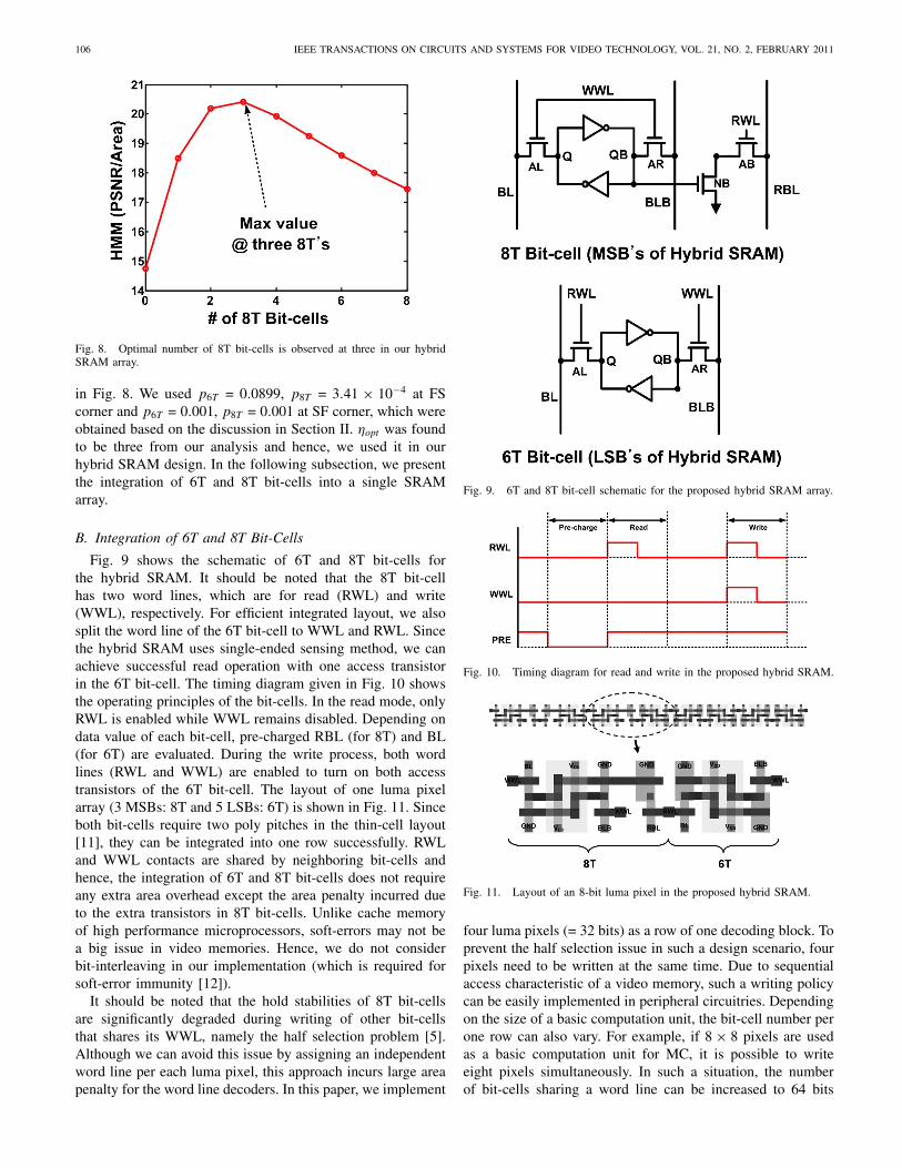
Fig. 8. Optimal number of 8T bit-cells is observed at three in our hybridSRAM array.
in Fig. 8. We used p6T = 0.0899, p8T = 3.41 × 10⁻⁴ at FScorner and p6T = 0.001, p8T = 0.001 at SF corner, which wereobtained based on the discussion in Section II. ηopt was foundto be three from our analysis and hence, we used it in ourhybrid SRAM design. In the following subsection, we presentthe integration of 6T and 8T bit-cells into a single SRAMarray.
B. Integration of 6T and 8T Bit-Cells
Fig. 9 shows the schematic of 6T and 8T bit-cells forthe hybrid SRAM. It should be noted that the 8T bit-cellhas two word lines, which are for read (RWL) and write(WWL), respectively. For efficient integrated layout, we alsosplit the word line of the 6T bit-cell to WWL and RWL. Sincethe hybrid SRAM uses single-ended sensing method, we canachieve successful read operation with one access transistorin the 6T bit-cell. The timing diagram given in Fig. 10 showsthe operating principles of the bit-cells. In the read mode, onlyRWL is enabled while WWL remains disabled. Depending ondata value of each bit-cell, pre-charged RBL (for 8T) and BL(for 6T) are evaluated. During the write process, both wordlines (RWL and WWL) are enabled to turn on both accesstransistors of the 6T bit-cell. The layout of one luma pixelarray (3 MSBs: 8T and 5 LSBs: 6T) is shown in Fig. 11. Sinceboth bit-cells require two poly pitches in the thin-cell layout[11], they can be integrated into one row successfully. RWLand WWL contacts are shared by neighboring bit-cells andhence, the integration of 6T and 8T bit-cells does not requireany extra area overhead except the area penalty incurred dueto the extra transistors in 8T bit-cells. Unlike cache memoryof high performance microprocessors, soft-errors may not bea big issue in video memories. Hence, we do not considerbit-interleaving in our implementation (which is required forsoft-error immunity [12]).
It should be noted that the hold stabilities of 8T bit-cellsare significantly degraded during writing of other bit-cellsthat shares its WWL, namely the half selection problem [5].Although we can avoid this issue by assigning an independentword line per each luma pixel, this approach incurs large areapenalty for the word line decoders. In this paper, we implement
Fig. 9. 6T and 8T bit-cell schematic for the proposed hybrid SRAM array.
Fig. 10. Timing diagram for read and write in the proposed hybrid SRAM.
Fig. 11. Layout of an 8-bit luma pixel in the proposed hybrid SRAM.
four luma pixels (= 32 bits) as a row of one decoding block. Toprevent the half selection issue in such a design scenario, fourpixels need to be written at the same time. Due to sequentialaccess characteristic of a video memory, such a writing policycan be easily implemented in peripheral circuitries. Dependingon the size of a basic computation unit, the bit-cell number perone row can also vary. For example, if 8 × 8 pixels are usedas a basic computation unit for MC, it is possible to writeeight pixels simultaneously. In such a situation, the numberof bit-cells sharing a word line can be increased to 64 bits
CHANG et al.: A PRIORITY-BASED 6T/8T HYBRID SRAM ARCHITECTURE FOR AGGRESSIVE VOLTAGE SCALING IN VIDEO APPLICATIONS 107
Fig. 12. Array architecture of a 32 kbit hybrid SRAM.
(= 8 pixels), further reducing overall area penalty of the wordline decoder.
C. Array Architecture of the Proposed Hybrid SRAM
Fig. 12 shows the array architecture of the proposed hybridSRAM. We assume that total array size is 32 kbit. As discussedin the previous subsection, we placed four luma pixels (= 32bits) on a row of one decoding block. To write these bit-cells at the same time, an independent write driver is assignedeach column of the bit-cell array. Our design consists offour decoding blocks and each block has eight sub-arrays.Since the proposed hybrid SRAM array uses single-ended readscheme, its architecture is implemented based on full-swingread method instead of sense amplifier approach. In such ascheme, read performance is mainly dependent on the numberof bit-cells per local read bitline. As mentioned earlier, thehybrid SRAM is proposed to achieve lower power dissipationwhen displaying CIF/QCIF format. Since these formats requirelow operating speed, we can add large number of bit-cells to alocal read bitline. However, in this paper, we assume that thevideo processor can switch its display mode to high qualityformat such as 1080p/720p (per 30 frames/s) [6]. In such ascenario, the SRAM needs to be operated at high frequencyof several hundred MHz. Hence, we determined the number ofbit-cells on a sub-array column to be 32. The simulation resultsof the following section show that this array architecturesatisfies the performance requirements successfully.
It should be noted that the “BL” node of a 6T bit-cell isused for both read and write unlike that of an 8T bit-cell(Fig. 9). For the read, the “BL” nodes of 6T bit-cells on a sub-array column are connected to a local read bitline (rbl#[31:0]).Meanwhile, they also need to be connected to a global writebitline (wbl#[31:0]) for the write. As a result, the global writebitline will be connected to the local bitline. However, in sucha situation, read performance is considerably degraded dueto large parasitic caps of the global write bitline. To handlethis issue, we insert transmission gates between bitlines of asub-array (bl#[31:0]) and global write bitlines (wbl#[31:0]),as shown in the figure, and turn on the transmission gates
Fig. 13. PSNR curves of 32 kbit 6T-only array at FS corner. (a) Akiyo.(b) Foreman. (c) Football.
during writes only. Under such a circumstance, the parasiticcaps of global write bitlines hardly affect read performance ofour design. The “BLB” nodes of bit-cells were not used forread and hence, we directly connected them to complementaryglobal write bitlines (wblb#[7:0]).
VI. Simulation Results
A. Output Quality Comparison (6T-Only Versus Hybrid)
Figs. 13 and 14 show video sequence simulation results oftwo designs (6T-only and the proposed hybrid), respectively.Here, we estimated PSNR values over whole sequences ofthree videos (Akiyo, Foreman, and Football). In the abovediscussions, we only considered errors in luma pixels. How-ever, in the simulations of Figs. 13 and 14, we also tookinto account the errors in motion vectors since motion vectorshave profound impact on video output quality. It should benoted that required array size for motion vectors is much
108 IEEE TRANSACTIONS ON CIRCUITS AND SYSTEMS FOR VIDEO TECHNOLOGY, VOL. 21, NO. 2, FEBRUARY 2011
Fig. 14. PSNR curves of 32 kbit hybrid SRAM array at VDD = 600 mV.(a) Akiyo. (b) Foreman. (c) Football.
smaller compared to that of luma pixels (0.7–0.8% of lumabits in a video image frame) [10]. Hence, in the proposedhybrid SRAM, we assume that the array of motion vectorswill be implemented as 8T-only. In such a scenario, overallarea penalty of the hybrid SRAM becomes 11.64% comparedto 6T-only array.
In Fig. 13, we used 6T-only array for the video memoryand considered two cases of supply power: VDD of 1-V and600 mV, respectively. We generated errors in the memoryarray with PF of FS corner, which is the worst case forthe 6T bit-cell, and obtained PSNR values from MATLABsimulations. At 600 mV VDD and FS corner, 6T bit-cells sufferfrom large read failure probability (= 0.0899) and hence,PSNR values are significantly degraded. Fig. 14 shows PSNRresults of the proposed hybrid SRAM array, which are alsosimulated at 600 mV. Since the worst PF of 6T and 8T appearsat different process corners (FS and SF respectively), weestimated PSNR values at these two corners. In spite of being
Fig. 15. Video output comparison under iso-area condition (6T-only versusthe proposed hybrid arrays). (a) Akiyo. (b) Foreman. (c) Football.
as low supply as 600 mV, the proposed hybrid SRAM arrayprovides high PSNR value. We captured video images duringthe simulations of Figs. 13 and 14, the results of which areshown in Appendix II. At 600 mV VDD, the video image of6T-only design suffers from impulse-like noises within macroblocks, resulting from the bit-cell failure of luma pixel array.Moreover, the errors of motion vector lead to corruptionsof entire macro-blocks. On the other hand, the proposedhybrid SRAM array delivers good output quality at 600 mV.The results successfully demonstrate that the proposed hybridSRAM array enables us to scale down VDD more aggressivelythan 6T-only array.
It should be noted that simple up-sizing of bit-cell tran-sistors can improve memory stability. As discussed above,the proposed hybrid SRAM incurs 11.64% area penalty. Forfair comparison, we should compare output qualities of twodesigns (6T-only versus the proposed hybrid arrays) under
CHANG et al.: A PRIORITY-BASED 6T/8T HYBRID SRAM ARCHITECTURE FOR AGGRESSIVE VOLTAGE SCALING IN VIDEO APPLICATIONS 109
Fig. 16. Read and write power comparisons for a 32 kbit bit-cell array underiso-area condition (6T-only versus hybrid).
iso-area condition. Fig. 15 shows PSNR comparison resultsunder iso-area condition, which also include the effect ofmotion vector errors. Due to grid problems, we cannot exactlyincrease transistor sizes by 11.64%. Hence, we used 1.15xlarger 6T bit-cells for the PSNR simulations of Fig. 15. Theresults show that the proposed hybrid SRAM array allowsroughly 100–150 mV supply over-scaling compared to the 6T-only array under iso-area condition.
B. Power Comparison (6T-Only Versus Hybrid)
Fig. 16 shows power comparison results for two designs(6T-only versus the proposed hybrid arrays) under iso-areacondition. Throughout the power simulations, memory oper-ating frequency was fixed to 10 MHz. Power dissipation ishighly correlated to process corner and temperature. Here,we estimated the power dissipation at TT corner and 25°C. For iso-area condition, large transistors are used for 6T-only array, resulting in the increase of load capacitances ofSRAM decoders. Hence, the power dissipation of 6T-onlyarray is a little larger compared to that of the proposedhybrid SRAM array. Moreover, our hybrid SRAM array allows100–150 mV over-scaling of VDD for similar image quality,providing significant power savings for both read and write (atleast 32% at 10 MHz frequency). The over-scaling contributesto reducing active leakage also. As shown in Fig. 17, leakagepower of the hybrid SRAM array at 600 mV is 28% less thanthat of the 6T-only array at 700 mV VDD.
C. Performance Simulation Results
Fig. 18 shows performance simulation results for the pro-posed hybrid SRAM array. We obtained these results at the
Fig. 17. Leakage power comparison for a 32 kbit bit-cell array under iso-area condition (6T-only versus hybrid).
Fig. 18. Performance simulation results of the 32 kbit hybrid SRAM array(at SS corner).
worst case process corner, which is SS corner for performance.For this simulation, we also considered temperature variationsacross −30 °C to 120 °C. At voltage as low as 600 mV VDD,diffusion current [14] is a substantial portion of the MOSFETdrive current. The diffusion current exponentially decreasesas the temperature is lowered [14] and hence, the worsttemperature for the performance is found at −30 °C. Theworst temperature corner for supply voltage of 800 mV and1-V is shown to be at 120 °C since drift current [14] mainlydetermines the performance at these voltage regions.
As mentioned in the above sections, CIF/QCIF displayformats require tens of MHz of operating frequency. It shouldbe noted that despite the worst process and temperature corner,our design shows 50 MHz performance at 600 mV VDD. Itdemonstrates that delay degradation resulting from loweringsupply to 600 mV can be considered as a minor issue forCIF/QCIF display formats. At 1-V VDD, our design couldbe operated at 600 MHz, which also successfully delivers theperformance requirements of high quality video formats suchas 1080p/720p.
VII. Conclusion
Large numbers of memory access is one of the majorsources of power dissipation of MPEG-4 video processor. Wecan significantly reduce the power by scaling down the supplyvoltage in memory. However, read stability of conventional6T SRAM bit-cells impedes supply scaling below a certain
110 IEEE TRANSACTIONS ON CIRCUITS AND SYSTEMS FOR VIDEO TECHNOLOGY, VOL. 21, NO. 2, FEBRUARY 2011
point. Although we can obtain more supply scaling using 8TSRAM bit-cells, large area overhead (beyond 30%) of the8T bit-cell limits its application. In this paper, we proposeda hybrid SRAM for video memory, where we implementedonly few MSB bits as 8T bit-cells and other bits as 6T bit-cells in a luma pixel. This approach allowed us to alleviatethe area overhead associated with 8T bit-cell only array. Itshould be noted that the human visual system is sensitivemainly to higher order bits of luminance pixels in videodata. Hence, we can scale down the supply voltage of videomemory more aggressively using the hybrid SRAM arraywithout compromising the output video quality significantly.We developed an algorithm to find an optimal number of 8Tbit-cells in a luma pixel. Using this algorithm, we found thatthree MSB bits are optimal for the 8T bit-cells in the 65 nmCMOS. Simulation results show that under iso-area condition,such a scheme provides 100–150 mV over-scaling comparedto 6T-only array. We implemented 32 kbit hybrid SRAM arrayin 65 nm CMOS and compared its power dissipation to that ofthe 6T-only array under iso-area condition. Due to the supplyover-scaling, we can achieve at least 32% power savings inthe hybrid SRAM array as compared to the 6T-only array (at10 MHz frequency).
Appendix I
The derivation of MSE per pixel in (4) is as follows. Letus consider an 8-bit luminance pixel without any error as A =∑7
i=0 ai2i and its counterpart with error as B =∑7
i=0 bi2i . TheMSE per pixel for number of 8T bit-cells equal to η is givenby the expression
MSEpixel(η) = E[(A − B)2
]= E
⎡⎣
(7∑
i=0
ai2i −
7∑i=0
bi2i
)2⎤⎦
= E
⎡⎣
(7∑
i=0
(ai − bi)2i
)2⎤⎦ .
Rewriting the expression within the expectation operator assum of error due to 6T bit-cells and 8T bit-cells, we have
MSEpixel(η) = E
⎡⎢⎣
⎛⎝7−η∑
i=0
(ai − bi)2i +
7∑j=8−η
(aj − bj)2j
⎞⎠
2⎤⎥⎦
where the first summation represents error due to 6T bit-cellsand the second term the error due to 8T bit-cells. Assumingindependence of Xi(= ai − bi) and Yj(= aj − bj), we have
MSEpixel(η) = E
⎡⎢⎣
⎛⎝7−η∑
i=0
Xi2i +
7∑j=8−η
Yj2j
⎞⎠
2⎤⎥⎦
(Xi = ai − bi, Yj = aj − bj)
= E
⎡⎣
(7−η∑i=0
Xi2i
)2⎤⎦ + E
⎡⎢⎣
⎛⎝ 7∑
j=8−η
Yj2j
⎞⎠
2⎤⎥⎦
+2E
⎡⎣
(7−η∑i=0
Xi2i
)⎛⎝ 7∑
j=8−η
Yj2j
⎞⎠
⎤⎦
= E
⎡⎣
(7−η∑i=0
Xi2i
)2⎤⎦ + E
⎡⎢⎣
⎛⎝ 7∑
j=8−η
Yj2j
⎞⎠
2⎤⎥⎦
+2E
[(7−η∑i=0
Xi2i
)]∗ E
⎡⎣
⎛⎝ 7∑
j=8−η
Yj2j
⎞⎠
⎤⎦
= E
⎡⎣
(7−η∑i=0
X2i 22i
)+
∑m
∑n �=m
(Xm2m)(Xn2n)
⎤⎦
+E
⎡⎣
⎛⎝ 7∑
j=8−η
Y 2j 22j
⎞⎠ +
∑m
∑n �=m
(Ym2m)(Yn2n)
⎤⎦
+2E
[(7−η∑i=0
Xi2i
)]∗ E
⎡⎣
⎛⎝ 7∑
j=8−η
Yj2j
⎞⎠
⎤⎦
=7−η∑i=0
E(X2i )22i +
7∑j=8−η
E(Y 2j )22j
+2
(7−η∑i=0
E(Xi)2i
)∗
⎛⎝ 7∑
j=8−η
E(Yj)2j
⎞⎠
⎛⎝ E
⎡⎣∑
m
∑n�=m
(Xm2m)(Xn2n)
⎤⎦
=∑m
∑n�=m
E[(Xm2m)]E[(Xn2n)] = 0
⎞⎠
(Xm, Xn and Ym, Yn are independent and E[Xm] =E[Xn] =0)
E(Xi) =∑
XipXi= 0 ∗ (1 − p6T ) + (+1) ∗ (p6T /2) + (−1)
(p6T /2) = 0
E(Yj) =∑
YjpYj= 0 ∗ (1 − p8T ) + (+1) ∗ (p8T /2) + (−1)
∗(p8T /2) = 0
E(X2i ) =
∑X2
i pXi= 02 ∗ (1 − p6T ) + (+1)2 ∗ (p6T /2) + (−1)2
∗(p6T /2) = p6T
E(Y 2j ) =
∑Y 2
j pYj= 02 ∗ (1 − p8T ) + (+1)2 ∗ (p8T /2) + (−1)2
∗(p8T /2) = p8T
(p6T = the 6T bit-cell failure probability,
p8T = the 8T bit-cell failure probability).
We substitute the above expectation values into the MSEexpression and use indicator functions to include the specialcases of η = 0 and η = 8. This yields the final expression forMSE as follows:
MSEpixel(η) = 1η=0
(7∑
i=0
p6T 22i
)+1η=8
(7∑
i=0
p8T 22i
)+1η∈[1,7]
⎛⎝7−η∑
m=0
p6T 22m +7∑
n=8−η
p8T 22n
⎞⎠
CHANG et al.: A PRIORITY-BASED 6T/8T HYBRID SRAM ARCHITECTURE FOR AGGRESSIVE VOLTAGE SCALING IN VIDEO APPLICATIONS 111
[1] MPEG [Online]. Available: http://www.mpeg4.org[2] C. Lin, P. Tseng, Y. Chiu, S. Lin, C. Cheng, H. Fang, W. Chao, and
L. Chen, “A 5 mW MPEG4 SP encoder with 2-D bandwidth-sharingmotion estimation for mobile application,” in Proc. ISSCC Dig. Tech.Papers, Feb. 2006, pp. 1626–1635.
[3] J. Rabaey, A. Chandrakasan, and B. Nicolic, Digital Integrated Circuits.Englewood Cliffs, NJ: Prentice-Hall, 2003.
[4] S. Mukhopadhyay, H. Mahmoodi, and K. Roy, “Statistical design andoptimization of SRAM cell for yield enhancement,” in Proc. IEEE/ACMInt. Conf. Comput.-Aided Design, Nov. 2004, pp. 10–13.
[5] L. Chang, R. K. Montoye, Y. Nakamura, K. A. Batson, R. J. Eicke-meyer, R. H. Dennard, W. Haensch, and D. Jamsek, “An 8T-SRAMfor variability tolerance and low-voltage operation in high-performancecaches,” IEEE J. Solid State Circuits, vol. 43, no. 4, pp. 956–963, Apr.2008.
[6] Y. Lin, D. Li, C. Lin, T. Kuo, S. Wu, W. Tai, W. Chang, and T. Chang,“A 242 mW 10 mm2 1080p H.264/AVC high-profile enocder chip,” inProc. ISSCC Dig. Tech. Papers, Feb. 2008, pp. 314–315.
[7] T. Liu, T. Lin, S. Wang, W. Lee, K. Hou, J. Yang, and C. Lee, “A125 µW, fully scalable MPEG-2 and H.264/AVC video decoder formobile applications,” IEEE J. Solid State Circuits, vol. 42, no. 1, pp.161–169, Jan. 2007.
[8] I. J. Chang, K. Kang, C. H. Kim, S. Mukhopadhyay, and K. Roy, “Fastand accurate estimation of nano-scaled SRAM read failure probabilityusing critical point sampling,” in Proc. CICC, Sep. 2005, pp. 439–442.
[9] K. Takeda, H. Ikeda, Y. Hagihara, M. Nomura, and H. Kobatake,“Redefinition of write margin for next-generation SRAM and write-margin monitoring circuit,” in Proc. ISSCC Dig. Tech. Papers, Feb. 2006,pp. 630–631.
[10] V. Bhaskaran and K. Konstantinides, Image and Video CompressionStandards, 2nd ed. Norwell, MA: Kluwer, 1997.
[11] K. Nii, Y. Tsukamoto, T. Yoshizawa, S. Imaolka, and H. Makino, “A90 nm dual-port SRAM with 2.04/spl mu/m/sup 2/8T-thin cell usingdynamically-controlled column bias scheme,” in Proc. ISSCC Dig. Tech.Papers, Feb. 2004, pp. 508–543.
[12] I. J. Chang, J. Kim, S. P. Park, and K. Roy, “A 32 kb 10T sub-thresholdSRAM array with bit-interleaving and differential read scheme in 90 nmCMOS,” IEEE J. Solid State Circuits, vol. 44, no. 2, pp. 650–658, Feb.2009.
112 IEEE TRANSACTIONS ON CIRCUITS AND SYSTEMS FOR VIDEO TECHNOLOGY, VOL. 21, NO. 2, FEBRUARY 2011
[13] I. J. Chang, D. Mohapatra, and K. Roy, “A voltage-scalable andprocess variation resilient hybrid SRAM architecture for MPEG-4 videoprocessors,” in Proc. DAC, Jul. 2009, pp. 670–675.
[14] Y. Taur and T. H. Ning, Fundametals of Modern VLSI Devices. Cam-bridge, U.K.: Cambridge Univ. Press, 2002.
Ik Joon Chang received the B.S. degree, withsumma cum laude, in electrical engineering fromSeoul National University, Seoul, Korea, and theM.S. degree from the School of Electrical andComputer Engineering, Purdue University, WestLafayette, IN, in 2002 and 2005, respectively. Cur-rently, he is pursuing the Ph.D. degree from PurdueUniversity.
In 2003, he was a Software Engineer with LGElectronics, Seoul. During 2007, he had an intern-ship with Qualcomm, San Diego, CA, where he
performed research related to low-power circuit techniques. His currentresearch interests include robust and low-power circuit design in nanoscaledcomplementary metal-oxide-semiconductor technologies.
Mr. Chang was awarded by the Samsung Scholarship Foundation in 2005.
Debabrata Mohapatra received the B.Tech. degreewith honors in electrical engineering and a minor inelectronic communication engineering from the In-dian Institute of Technology Kharagpur, Kharagpur,India, in 2005. He is currently pursuing the Ph.D.degree from the School of Electrical and ComputerEngineering, Purdue University, West Lafayette, IN.
He was with the Memory Design Group, Qual-comm, San Diego, CA, in 2008. His current researchinterests include low-power, process-variation awarecircuit, and system design for multimedia hardware
in nanometer technologies.
Kaushik Roy (F’01) received the B.Tech. degreein electronics and electrical communications en-gineering from the Indian Institute of Technol-ogy Kharagpur, Kharagpur, India, and the Ph.D.degree from the Department of Electrical and Com-puter Engineering, University of Illinois at Urbana-Champaign, Urbana, in 1990.
He was with the Semiconductor Process and De-sign Center, Texas Instruments, Dallas, where heworked on field-programmable gate array architec-ture development and low-power circuit design. He
joined the Department of Electrical and Computer Engineering, PurdueUniversity, West Lafayette, IN, in 1993, as a Faculty Member, where he iscurrently a Professor and the Roscoe H. George Chair with the Department ofElectrical and Computer Engineering. He has published more than 500 papersin refereed journals and conferences, holds 15 patents, graduated more than45 Ph.D. students, and is the co-author of two books, Low Power CMOS VLSIDesign (New York: Wiley and McGraw-Hill). His current research interestsinclude spintronics, very large-scale integrated (VLSI) design/computer-aideddesign for nanoscale silicon and non-silicon technologies, low-power elec-tronics for portable computing and wireless communications, VLSI testingand verification, and reconfigurable computing.
Dr. Roy received the National Science Foundation Career DevelopmentAward in 1995, the IBM Faculty Partnership Award, the ATT/Lucent Founda-tion Award, the SRC Technical Excellence Award in 2005, the SRC InventorsAward, the Purdue College of Engineering Research Excellence Award, theHumboldt Research Award in 2010, and the Best Paper Awards at the Inter-national Test Conference in 1997, IEEE International Symposium on Qualityof IC Design in 2000, IEEE Latin American Test Workshop in 2003, IEEENano in 2003, IEEE International Conference on Computer Design in 2004,IEEE/ACM International Symposium on Low Power Electronics and Designin 2006, and the IEEE Circuits and System Society Outstanding Young AuthorAward (Chris Kim) in 2005, and the IEEE Transactions on VLSI SystemsBest Paper Award in 2006. He is the Purdue University Faculty Scholar.He was a Research Visionary Board Member of Motorola Laboratories in2002. He has been on the Editorial Board of IEEE Design and Test, IEEETransactions on Circuits and Systems, and IEEE Transactions on
Very Large Scale Integration Systems. He was the Guest Editor fora special issue on “low-power VLSI” in IEEE Design and Test in 1994,IEEE Transactions on Very Large Scale Integration Systems inJune 2000, and IEE Proceedings—Computers and Digital Techniques in July2002.