Page 1
© Prismark Partners LLC
1
PRISMARK PRESENTATION
PREPARED FOR:
13th EUROPEAN MANUFACTURING TEST CONFERENCE
(EMTC) October 8, 2014
A RAPIDLY CHANGING TEST LANDSCAPE
PREPARED BY:
Brian Swiggett Managing Partner
PRISMARK PARTNERS LLC 130 Main Street Cold Spring Harbor NY 11724
Tel: 631 367-9187 Fax: 631 367-9223 e-mail: [email protected]
www.prismark.com
Page 2
© Prismark Partners LLC
2
N514.239bes-drivers2
$0
$500
$1,000
$1,500
$2,000
$2,500
$Bn
2009 2010 2011 2018F201720162012 2013 2014E 2015
THE DRIVERS OF THE ELECTRONICS INDUSTRY HAVE CHANGED
23%19% 6.5%
2.9%10% 0%
4.1%82%
91%
37% 29.1%10.2%
2.8%
5.1%
-0.1%
-1% 0.8%
3% 4.1%
-7%-3.3%
13%
9%
4.3%
$1,269Bn
$1,458Bn14.9%
$1,602Bn9.9%
$1,616Bn0.9%
$1,678Bn3.8%
$1,731Bn3.2%
$2,020Bn2013-2018
CAAGR 3.8%
Note: Includes value of PV modules in total electronics
Automotive Electronics
Other Electronics
Servers/Storage/Comm infrastructure
Smartphones and Tablets
Page 3
© Prismark Partners LLC
3
A MATURE ELECTRONICS INDUSTRY
GROWS FASTER AT THE PERIPHERY
• Electronics Infrastructure Builds Out First – Computing and communications convergence – Continuing evolution and improvement – performance driven – Cloud and fog backbone
• Access at the Periphery Accelerates Later – Greater proportion of “consumer” and portable products drives integration – Explosion of new access points (ubiquitous networks) – Sensors and microsystems – “Internet of Things”
514.9/280bes
Page 4
© Prismark Partners LLC
4
MOBILE PHONES: MORE FUNCTION PER AREA
260x
4x
100x
2,300x
3x
4,000x
35x
25x
9x
15x
4x
1x
0.3x
0.8x
0.25x
2x
1x
2003
Nokia 6650
2013
Apple iPhone 5S Wireless Data Rate
Wireless Bands/Modes
Processor Speed
User Memory
Display Size
Display Colors
Display Pixels
Camera Resolution
Sensors
Battery Size
Battery Life
Price
Volume
Weight
PCB Area
Silicon Area
Silicon Area (excl. Memory)
514.4/407mvc
The space and cost constraints associated with consumer devices drives electronic integration
Page 5
© Prismark Partners LLC
5
N314.146mvc-Segmentation
>$600
Apple
Samsung
LG
Lenovo
Huawei
Coolpad
ZTE
% of Smartphones
$450 - $600
$300 - $450
$150 - $300
<$150
2011
Smartphone ASPUnits
Premium segment remains But most growth in low-cost smartphones
475M$366
680M$338
1,190M$270
980M$295
1,700M$200
1,600M$210
1,500M$220
1,400M$240
2012 2013 2014F 2015F 2016F 2018F2017F
SMARTPHONE ASP SEGMENTATION
Center of gravity shifts to lower-priced smartphones
Page 6
© Prismark Partners LLC
6
Markets evolve and opportunity (units) increase
Internet of Computers
Mainframe Networking Cloud Fog
Internet of People Internet of Things
THE NEXT PHASE OF GROWTH
Devices becoming smaller and thinner
Infrastructure becomes pervasive
Minicomputer
1980 1990 2000 2010 2020
10M+Units
100M+Units
1Bn+Units
5Bn+Units
30Bn+
UnitsPC
Desktop
Internet
Mobile
Internet
Wearable/IoT
814.10/416rd
Page 7
© Prismark Partners LLC
7
DRIVERS FOR INTERNET OF THINGS
AND WEARABLE ELECTRONICS
• Factors Driving Demand for Connected Devices:
– Convenience
• Get info or act/react now, wherever you are
– Health
• Monitor vitals continuously, detect and react to emergencies
– Safety
• Monitor and detect processes (home, car, factory,
environment) and respond
– Efficiency
• Streamline processes, save energy (avoid traffic,
turn heat/lights on/off)
• Technology Drivers
– MCU price/performance
– Low cost MEMS sensors
– Wireless connectivity costs – WiFi, Bluetooth, Zigbee, cellular
– Smart phone (or automobile) as a gateway
– Cloud-based infrastructure
– High energy density power sources
814.10/416rd
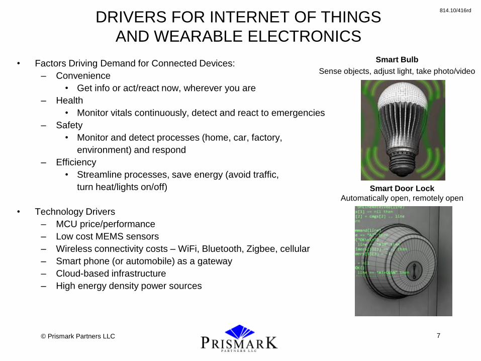
Smart Bulb
Sense objects, adjust light, take photo/video
Smart Door Lock
Automatically open, remotely open
Page 8
© Prismark Partners LLC
8
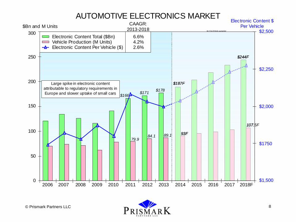
AUTOMOTIVE ELECTRONICS MARKET
0
50
100
150
250
200
300
$1,500
$1750
$2,000
$2,250
$2,500
2007 2009 2011 2013 2014 2017 2018F2015 20162006 2008 2010 2012
$Bn and M UnitsElectronic Content $
Per VehicleCAAGR:
2013-2018
Electronic Content Total ($Bn) 6.6%Vehicle Production (M Units) 4.2%Electronic Content Per Vehicle ($) 2.6%
Large spike in electronic content
attributable to regulatory requirements in
Europe and slower uptake of small cars
79.984.1
$171$166
Kc314.016rd-automkt
89.1
$178
$187F
$244F
107.5F
93F
Page 9
© Prismark Partners LLC
9
CHANGING IC TEST LANDSCAPE
• Consequences of growth at the “periphery”
– Increasing small form factor IC content – WLP, FC, 3D, embedded
– SiP integration
– Wireless access
– Sensors proliferate
– High volume, low-cost pressure, time-to-market driven
– More complex packaging and test challenges
Page 10
© Prismark Partners LLC
10
300
Bn UnitsKc1013.088bp-ic shipments
250
150
50
0
1980 1985 1990 1995 2000 2005 2010 2020
By 2020, non-leaded packages will account formore than 50% of all ICs
2015
100
200
IC SHIPMENTS BY PACKAGE CATEGORY
3D
Bare Die (COB)
Through Hole (DIP)
Surface Mount (SO, QFP)
Modified Leadframe (QFN, MLF)
Wire Bond Array Package (BGA, CSP, LGA)
Flip Chip Array Package
Direct Flip Chip (DCA, WLCSP)
Page 11
© Prismark Partners LLC
11
314.1/267bp
IC PACKAGE UNIT GROWTH
Package Type
(Bn Units) 2011
% of
Total 2013 2018
% of
Total
CAAGR
2013-2018
Traditional Leadframe
(SO, TSOP, QFP) 101 54% 102 108 40% 1.2%
QFN 21 11% 27 56 21% 16%
Wire Bond CSP
(includes stacked & BOC/DRAM) 28 15% 27 29 11% 0.9%
Wire Bond BGA
(> 19mm package size) 1.1 0.6% 0.9 0.8 0.3% -2.3%
Wire Bond Bare Die
(COB) 11 6% 12 16 6% 5.3%
Flip Chip CSP
(includes DRAM) 1.5 0.8% 4.4 13.4 5% 25%
Flip Chip BGA/PGA/LGA
(> 19mm Package Size) 1.1 0.6% 1.0 1.0 0.4% 0%
Wafer CSP 15 8% 19 35 13% 13%
COF/COG for Display Drivers 7.9 4% 8.7 11.1 4% 4.1%
TOTAL 186.7 100% 202.1 269.4 100% 5.9%
Page 12
© Prismark Partners LLC
12
Kc314.088bp-pitch trends
ARRAY PACKAGE PITCH TRENDS (BGA, CSP, PGA, LGA, WLCSP)(Excludes Small Die DCA, Display Drivers, and RF Modules)
1.27mm0
2008 2009 2010 2011 2012 2013 2014 2015 2016 2017 2018
10
20
30
40
50
60
70
Bn Units
1.0mm
0.5mm
0.65-0.8mm
0.4-0.45mm
0.3-0.35mm
DCA in Module
Sub 0.5mm was 2% of overall volume in 2008. By 2018 this will increase to 28% or 19Bn units
Page 13
© Prismark Partners LLC
13
APPLE A7 PROCESSOR
• Found in iPhone 5S – 28nm, 1.3GHz – 1GB LPDDR3 as PoP (64-bit) – Top package has 456 balls @0.35mm pitch
• ~14 x 15.5 x 1.0mm PoP
– ~1330 balls @ 0.4mm pitch – LDP/TMV PoP with die back side exposed – Molded underfill
• 10.3 x 9.9mm die – 95µm thick – 150/170µm Sn bump pitch – 65µm bump height, 75µm bump diameter
• 2-2-2 substrate – 360µm thick – 75µm vias, 27µm L/S – Laser via in glass reinforced core – 25µm dielectric and copper thickness
1013.6/193bp
Photo source: Prismark/Binghamton University
400µm
650µm
Page 14
© Prismark Partners LLC
14
0Bn
5Bn
10Bn
15Bn
20Bn
Annual Volume
1995 2000 2005 2010 2015 2020
WLCSP/DCA TIMELINE
kc313.085bp-timeline
5x5-7x7mm5x5-6x6mm
4x4mm
Die Size
4x4mm
1x1-2x3mm
EEPROM, MCU,
Security Chips, Watches
AdditionalDevice Types:Analog, IPD,
MOSFET
Bluetooth,WLAN, TV Chip,
Transceiver
Transceiver, Power
Manager, Image Sensor, Audio Codec
Combo/Connectivity, MCU
Wider adoption outside portable products,
expect up to 8x9mm die size
Wide adoption in
smartphones
Nokia phones with 7-8WLCSP
Page 15
© Prismark Partners LLC
15
BUMPED WAFER PRODUCTION BY PITCH(300mm Equivalent)
2013 2018
50-80 m(TCB)
3%
µ50-80 m(TCB)
1%
µ
100-150 m35%
µ
130-170 m(Solder or
Copper Bump)20%
µ
150-200 m20%
µ
175-250 m
30%
µ(Solder or Copper Bump)
200-800 m30%
µ
300-800 m
30%
µ(Ball Placement)
20-40 m12%
µ30-50 m
(19%
µGold Bump)
Note: Excludes microbump for TSV applications
TOTAL: 14M Wafers TOTAL: 27M Wafers
CAAGR 14%
Kc314.261bp-pitch
Page 16
© Prismark Partners LLC
16
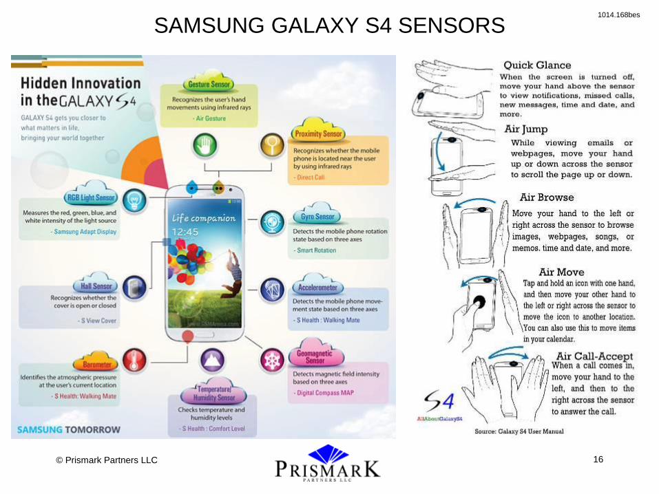
SAMSUNG GALAXY S4 SENSORS 1014.168bes
Page 17
© Prismark Partners LLC
17
GLOBAL MEMS MARKET
2013 2018 CAAGR
2013 – 2018
Units (Bn)
Value ($Bn)
Units (Bn)
Value ($Bn)
Units Value
Inkjet Heads 0.8 1.8 0.8 1.7 0% -1%
DLP 0.01 0.7 0.01 0.7 0% 0%
Pressure Sensors 0.7 1.9 1 2.5 7% 6%
MicroFluidics 0.5 1.2 1.2 2 19% 11%
Accelerometers 2.3 1.8 1.7 1.3 -6% -6%
Gyroscopes 0.65 1.5 0.7 1.5 1% 0%
Digital Compass 0.7 0.6 0.05 0.03 -41% -45%
Combo (Gyro/Accel/Compass) 0 0 1.9 3.7
MEMS Microphones 2.6 0.9 4 1.1 9% 4%
BAW Filters 1 0.3 1.5 0.4 8% 6%
RF MEMS 0.05 0.08 0.3 0.3 43% 30%
Others 0.2 0.3 0.5 0.6 20% 15%
TOTAL 9.51 11.1 13.7 15.8 8% 7%
613.6/099bp
Page 18
© Prismark Partners LLC
18
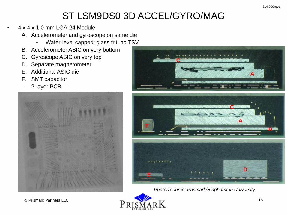
ST LSM9DS0 3D ACCEL/GYRO/MAG • 4 x 4 x 1.0 mm LGA-24 Module
A. Accelerometer and gyroscope on same die
• Wafer-level capped; glass frit, no TSV
B. Accelerometer ASIC on very bottom
C. Gyroscope ASIC on very top
D. Separate magnetometer
E. Additional ASIC die
F. SMT capacitor
– 2-layer PCB
A
C
C
A
B F
Photos source: Prismark/Binghamton University
E D
814.099mvc
Page 19
© Prismark Partners LLC
19
0214.1/105bp
SiP/MCP FORECAST
Product/Package Type Volume (Bn Units)
2013 2018
Forecast Leading Suppliers/Players
Stacked Die In Package and Memory Card
8 11 ASE, SPIL, Amkor, STATS ChipPAC, Samsung,
Micron, SKHynix, Toshiba, SanDisk
Stacked Package on Package – Bottom Package Only
0.8 1.3 Amkor, STATS ChipPAC, ASE, SPIL, Samsung,
Apple, Qualcomm, Sony, Panasonic
PA Centric RF Module 4.3 6.3 RFMD, Skyworks, Anadigics, Renesas,
TriQuint, Avago
Connectivity Module (Bluetooth/WLAN)
0.4 0.5 Murata, Taiyo Yuden, ACSIP, ALPS
Graphics/CPU or ASIC MCP 0.2 0.2 Intel, IBM, Fujitsu, Xlinx, Altera
Leadframe Module (Power/Other)
3 5 NXP, STMicro, TI, Freescale, Toshiba,
Infineon, Renesas, IR, ON Semi
MEMS and Controller 5 8 ST, Analog, Bosch, Freescale, Knowles,
SKHynix, InvenSense Denso
TOTAL 21.7 32.3
Page 20
© Prismark Partners LLC
20
DEVICE LEVEL TRENDS SUMMARY
• Package size reduction is ongoing, but pitch limitations draw a logical path
towards modular and 3D approaches
• A few clear trends are enabling miniaturization
– Fine Pitch Array Packages (0.5 0.4 0.35 0.3/0.25mm)
– Stacked Die (Memory) and Package Stacks (Logic/Memory)
– Wafer Level CSP
– Reduced Z-height Packages (0.3 to 0.6mm)
• 3D-TSV and Silicon Interposer approaches are still in development, with high-
volume products expected in the next three to five years
– Process integration and materials challenges remain
– Thermal, test, and logistics issues
1014.267bes
Page 21
© Prismark Partners LLC
21
PCB EMBEDDED COMPONENTS
• In Volume Production for Modules
Integration of passives and active die
Focus on camera, power management, connectivity, and RF modules
Over one decade of low-volume examples coming from Japan
Continued challenges in process (yield) and infrastructure
No current known production of embedded in main PCB
Embedded passives in IC packages now common for Samsung, Qualcomm, Apple; others such as MediaTek are following suit
• Market Estimates
Embedded actives approaching 200M modules on annual basis
Embedded passives in substrate will become standard practice in mobile products
A few key design wins drive high volumes
• Major Players
DNP, Unimicron, TDK-EPC, Taiyo Yuden, AT&S, SEMCO, CMK, Kyocera Circuit Solutions, Panasonic, Oki, Kinsus, Ibiden, Shinko, etc
Imbera-Daeduck JV lost funding and shut down; IP sold to GE
Historic Leaders such as DNP, CMK, and Kyocera Circuit Solutions have reduced focus
514.7/333bp
Page 22
© Prismark Partners LLC
22
EPCOS BLUETOOTH LE MODULE
• Smallest Module Using PCB Embedding Technology
– Bluetooth Smart (Bluetooth 4.0 Low Energy)
– Only needs power supply and antenna
– 4.6 x 5.6 x 1.0mm
– Targeted at wearable devices
• TDK’s Proprietary SESUB Technology
– Four-layer, 0.3mm thick SESUB substrate
– 0.1mm thick IC embedded between layers two and three
– Quartz resonator, bandpass filter, passives on top
– In volume production at 0.3M units per month
614.333mvc
11 x 6.8 x 1.85mm
Page 23
© Prismark Partners LLC
23
RAPIDLY CHANGING TEST LANDSCAPE
• Tester interfaces and handling systems will need to continue to adapt to evolving IC functional and physical packaging changes driven by high-volume consumer portables and emerging IoT applications
• Within five years, more than 50% of all devices will be delivered in non-traditional packages, WLP, bare die, or modules
• Sensor integration within high-volume, cost-sensitive applications will create especially difficult test challenges
• The good news is that these changes are creating opportunities for new test-related equipment and software solutions
Page 24
© Prismark Partners LLC
24
THANK YOU
The Ultimate Test Methodology?