173


A RECONFIGURABLE HARDWARE IMPLEMENTATION OF
GENETIC ALGORITHMS FOR VLSI CAD DESIGN
A Thesis
Presented to
The Faculty of Graduate Studies
of
The University of Guelph
by
GURWANT KAUR KOONAR
In partial fulfilment of requirements
for the degree of
Master of Science
July, 2003
c©Gurwant Kaur Koonar, 2004

2

ABSTRACT
A RECONFIGURABLE HARDWARE IMPLEMENTATION OF
GENETIC ALGORITHMS FOR VLSI CAD DESIGN
Gurwant Kaur Koonar
University of Guelph, 2003
Advisor:
Professor Shawki Areibi
The use of integrated circuits in high-performance computing, telecommunications
and consumer electronics has been growing at a very fast pace. Due to increasing com-
plexity of VLSI circuits, there is a growing need for efficient CAD tools. Partitioning is
a technique, widely used to solve diverse problems occuring in VLSI CAD. Several tech-
niques (heuristics) are available to solve the circuit partitioning problem ranging from
local search technique to advanced Meta-heuristics.
A Genetic Algorithm (GA) is a robust problem solving method based on natural
selection and can be used for solving a wide range of problems, including the problem of
circuit partitioning. Although, a GA can provide very good solutions for the problem of
circuit partitioning, the amount of computations and iterations required for this method
is enormous. As a result, software implementations of GA can become extremely slow for
large circuit partitioning problems. An emerging technology capable of providing high
computational performance on a diversity of applications is reconfigurable computing, also
known as adaptive computing, and FPGA-based computing. Implementing algorithms

directly in hardware, on the level of circuits, significantly reduces the control overhead
and large speedups can be obtained.
In this research, an architecture for implementing Genetic Algorithms on an FPGA
is proposed. The architecture employs a combination of pipelining and parallelization to
achieve speedups over software based GA. The proposed design was coded in VHDL and
was functionally verified by writing a testbench and simulating it using ModelSim. The
design was synthesized on Virtex part xcv2000e using Xilinx ISE 5.1. The GA processor
proposed in this thesis achieves more than 100× improvement in processing speed as
compared to the software implementation. The proposed architecture is discussed in
detail and the results are presented and analyzed.

Acknowledgements
I would like to express my gratitude to my advisors Dr. Shawki Areibi and Dr. Med-
hat Moussa for their invaluable assistance with this thesis and guidance throughout
my graduate studies. I would also like to thank Dr. Bob Dony for being in my com-
mittee. Special thanks to my loving husband for his support and advice throughout
this research. Without his help, this work would never have been possible. Finally,
I would like to thank my parents who encouraged me and gave me the will to
continue.
i

To
my family
whose love and encouragement helped accomplish this
thesis.
ii
Contents
1 Introduction 2
1.1 Reconfigurable Hardware . . . . . . . . . . . . . . . . . . . . . . . . 4
1.2 Genetic Algorithms . . . . . . . . . . . . . . . . . . . . . . . . . . . 7
1.3 Motivation . . . . . . . . . . . . . . . . . . . . . . . . . . . . . . . . 9
1.4 Contributions . . . . . . . . . . . . . . . . . . . . . . . . . . . . . . 12
1.5 Thesis Outline . . . . . . . . . . . . . . . . . . . . . . . . . . . . . . 13
2 Background 14
2.1 Overview of Circuit Partitioning(CP) . . . . . . . . . . . . . . . . . 14
2.1.1 0-1 Linear Programming Formulation of Netlist Partitioning 16
2.1.2 Complexity of Circuit Partitioning . . . . . . . . . . . . . . 18
2.1.3 Heuristic Search Techniques . . . . . . . . . . . . . . . . . . 19
2.1.4 Benchmarks . . . . . . . . . . . . . . . . . . . . . . . . . . . 21
2.2 Genetic Algorithm (GA) as an optimization method . . . . . . . . . 23
2.2.1 Characteristics of Genetic Search . . . . . . . . . . . . . . . 23
2.2.2 Main Components of Genetic Search . . . . . . . . . . . . . 24
2.2.3 GA Implementation . . . . . . . . . . . . . . . . . . . . . . . 30
iii

2.2.4 Mapping Genetic Algorithm to Hardware . . . . . . . . . . . 34
2.3 Overview of Field Programmable Gate Arrays . . . . . . . . . . . . 34
2.4 Overview of Reconfigurable Computing Systems . . . . . . . . . . . 38
2.5 Previous work in Hardware based GA . . . . . . . . . . . . . . . . . 41
2.5.1 Specific Architectures to speed GA . . . . . . . . . . . . . . 42
2.6 Summary . . . . . . . . . . . . . . . . . . . . . . . . . . . . . . . . 50
3 Architecture 51
3.1 System Specifications and Constraints . . . . . . . . . . . . . . . . 51
3.2 System Architecture . . . . . . . . . . . . . . . . . . . . . . . . . . 54
3.2.1 Detailed Internal Architecture . . . . . . . . . . . . . . . . . 57
3.2.2 Core Generics . . . . . . . . . . . . . . . . . . . . . . . . . . 63
3.2.3 Core Memories . . . . . . . . . . . . . . . . . . . . . . . . . 64
3.2.4 Pin Description . . . . . . . . . . . . . . . . . . . . . . . . . 65
3.3 Representation for Circuit-Partitioning . . . . . . . . . . . . . . . . 68
3.4 Selection Module . . . . . . . . . . . . . . . . . . . . . . . . . . . . 69
3.4.1 Pin Description . . . . . . . . . . . . . . . . . . . . . . . . . 70
3.4.2 Functional Description . . . . . . . . . . . . . . . . . . . . . 70
3.5 Crossover and Mutation Module . . . . . . . . . . . . . . . . . . . . 74
3.5.1 Pin Description . . . . . . . . . . . . . . . . . . . . . . . . . 74
3.5.2 Functional Description . . . . . . . . . . . . . . . . . . . . . 74
3.6 Fitness Module . . . . . . . . . . . . . . . . . . . . . . . . . . . . . 80
3.6.1 Pin Description . . . . . . . . . . . . . . . . . . . . . . . . . 80
3.6.2 Functional Description . . . . . . . . . . . . . . . . . . . . . 82
iv

3.7 Main Controller Module . . . . . . . . . . . . . . . . . . . . . . . . 85
3.7.1 Pin Description . . . . . . . . . . . . . . . . . . . . . . . . . 85
3.7.2 Functional Description . . . . . . . . . . . . . . . . . . . . . 85
3.8 Simulation and Verification . . . . . . . . . . . . . . . . . . . . . . 93
3.9 Summary . . . . . . . . . . . . . . . . . . . . . . . . . . . . . . . . 98
4 Implementation and Mapping 99
4.1 Overview and System Operation of RPP . . . . . . . . . . . . . . . 99
4.2 Implementation Details . . . . . . . . . . . . . . . . . . . . . . . . . 101
4.2.1 System Description for Top level Implementation . . . . . . 102
4.2.2 Functional description of the Logic-module FPGA design . . 104
4.2.3 Address Mapping . . . . . . . . . . . . . . . . . . . . . . . . 109
4.3 Results and Conclusions . . . . . . . . . . . . . . . . . . . . . . . . 109
4.4 Summary . . . . . . . . . . . . . . . . . . . . . . . . . . . . . . . . 111
5 Conclusions and Future Directions 113
5.1 Future Work . . . . . . . . . . . . . . . . . . . . . . . . . . . . . . . 114
5.1.1 Architecture Enhancements . . . . . . . . . . . . . . . . . . 114
5.1.2 Platform-mapping Enhancements . . . . . . . . . . . . . . . 115
A Introduction to AMBA Buses 116
A.1 Overview of the AMBA specification . . . . . . . . . . . . . . . . . 116
A.2 A typical AMBA-based microcontroller . . . . . . . . . . . . . . . . 117
A.3 Terminology . . . . . . . . . . . . . . . . . . . . . . . . . . . . . . . 119
A.4 Introducing the AMBA AHB . . . . . . . . . . . . . . . . . . . . . 120
v

A.4.1 Overview of AMBA AHB operation . . . . . . . . . . . . . . 122
A.4.2 Basic Transfer . . . . . . . . . . . . . . . . . . . . . . . . . . 123
A.4.3 Address Decoding . . . . . . . . . . . . . . . . . . . . . . . . 125
A.4.4 AHB Bus Slave . . . . . . . . . . . . . . . . . . . . . . . . . 126
A.4.5 AMBA AHB signal list . . . . . . . . . . . . . . . . . . . . . 126
B Overview of Rapid Prototyping Platform 130
B.1 Overview of the Integrator/AP . . . . . . . . . . . . . . . . . . . . 130
B.2 Overview of Core Module . . . . . . . . . . . . . . . . . . . . . . . 134
B.3 Overview of Logic Module . . . . . . . . . . . . . . . . . . . . . . . 137
B.4 Rapid Prototyping Platform Design Flow . . . . . . . . . . . . . . . 138
C VHDL Code 141
C.1 GaTop.vhd . . . . . . . . . . . . . . . . . . . . . . . . . . . . . . . 141
C.2 test bench.vhd . . . . . . . . . . . . . . . . . . . . . . . . . . . . . . 147
Bibliography 156
vi
List of Tables
2.1 Benchmarks used as test cases . . . . . . . . . . . . . . . . . . . . . 22
2.2 Statistical information of benchmarks . . . . . . . . . . . . . . . . . 22
3.1 Register address map . . . . . . . . . . . . . . . . . . . . . . . . . . 60
3.2 Generics used in the design . . . . . . . . . . . . . . . . . . . . . . . 63
3.3 Core Memories . . . . . . . . . . . . . . . . . . . . . . . . . . . . . 64
3.4 Pin description of Top level GA processor(part1) . . . . . . . . . . . 66
3.5 Pin description of Top level GA processor(part2) . . . . . . . . . . . 67
3.6 Pin description of Selection Module . . . . . . . . . . . . . . . . . . 71
3.7 Pin description of Crossover Module . . . . . . . . . . . . . . . . . 75
3.8 Pin description of fitness Module . . . . . . . . . . . . . . . . . . . 81
3.9 Pin description of Main Controller(part1) . . . . . . . . . . . . . . . 86
3.10 Pin description of Main Controller(part2) . . . . . . . . . . . . . . . 87
3.11 Default GA parameters . . . . . . . . . . . . . . . . . . . . . . . . . 93
3.12 Software Fitness Results . . . . . . . . . . . . . . . . . . . . . . . . 94
3.13 Hardware Fitness Results . . . . . . . . . . . . . . . . . . . . . . . 94
3.14 Performance results for Hardware GA and Software GA for different
Generation Count . . . . . . . . . . . . . . . . . . . . . . . . . . . . 95
vii

3.15 Performance results for Hardware GA and Software GA for different
population size . . . . . . . . . . . . . . . . . . . . . . . . . . . . . 96
3.16 Synthesis Report . . . . . . . . . . . . . . . . . . . . . . . . . . . . 97
4.1 RPP test results with different generation counts for different Bench-
marks . . . . . . . . . . . . . . . . . . . . . . . . . . . . . . . . . . 110
A.1 AMBA AHB signals(part1) . . . . . . . . . . . . . . . . . . . . . . 128
A.2 AMBA AHB signals(part2) . . . . . . . . . . . . . . . . . . . . . . 129
viii

List of Figures
1.1 Trade-off between flexibility and performance. . . . . . . . . . . . . 5
1.2 Overall Design Flow . . . . . . . . . . . . . . . . . . . . . . . . . . 10
2.1 Illustration of circuit partitioning . . . . . . . . . . . . . . . . . . . 15
2.2 Representation schemes and genetic operators . . . . . . . . . . . . 26
2.3 Genetic Operators . . . . . . . . . . . . . . . . . . . . . . . . . . . 29
2.4 A generic Genetic Algorithm . . . . . . . . . . . . . . . . . . . . . . 31
2.5 Field Programmable Gate Arrays . . . . . . . . . . . . . . . . . . . 35
2.6 FPGA with a two dimensional array of logic blocks. . . . . . . . . . 36
2.7 Configurable Logic Block. . . . . . . . . . . . . . . . . . . . . . . . 37
2.8 Design Steps for Reconfigurable Computing. . . . . . . . . . . . . . 40
3.1 Hardware software Design Comparison. . . . . . . . . . . . . . . . . 55
3.2 Architecture for the Genetic Algorithm Processor. . . . . . . . . . . 58
3.3 Interaction of Host with Genetic Algorithm Processor. . . . . . . . 59
3.4 CMlength Register . . . . . . . . . . . . . . . . . . . . . . . . . . . 60
3.5 NetNum Register . . . . . . . . . . . . . . . . . . . . . . . . . . . . 61
3.6 PopSiz Register . . . . . . . . . . . . . . . . . . . . . . . . . . . . . 61
ix

3.7 GenNum Register . . . . . . . . . . . . . . . . . . . . . . . . . . . . 62
3.8 CrossoverRate Register . . . . . . . . . . . . . . . . . . . . . . . . . 62
3.9 MutationRate Register . . . . . . . . . . . . . . . . . . . . . . . . . 63
3.10 Pin description of top level GA Processor . . . . . . . . . . . . . . . 65
3.11 Representation of chromosome and netlist for circuit-partitioning. . 68
3.12 Pin description of Selection Module . . . . . . . . . . . . . . . . . . 69
3.13 Detailed description of Selection Module. . . . . . . . . . . . . . . . 72
3.14 State Diagram of Selection Module . . . . . . . . . . . . . . . . . . 73
3.15 Pin description of Crossover and Mutation Module . . . . . . . . . 76
3.16 Address generation for the Chromosome Memory. . . . . . . . . . . 77
3.17 Detailed Description of Crossover and Mutation Module. . . . . . . 78
3.18 Detailed Description of Crossover and Mutation Module logic. . . . 79
3.19 Pin description of Fitness Module . . . . . . . . . . . . . . . . . . . 80
3.20 Fitness Calculation. . . . . . . . . . . . . . . . . . . . . . . . . . . . 83
3.21 Detailed Description of Fitness . . . . . . . . . . . . . . . . . . . . 84
3.22 Pin description of Main Controller Module . . . . . . . . . . . . . . 88
3.23 Control Register write Timings . . . . . . . . . . . . . . . . . . . . 89
3.24 Control Input data and control Timings . . . . . . . . . . . . . . . 89
3.25 Core output data and control timings . . . . . . . . . . . . . . . . . 89
3.26 Single port memory access timings . . . . . . . . . . . . . . . . . . 90
3.27 Dual port memory access timings . . . . . . . . . . . . . . . . . . . 90
3.28 Detailed Description of Main Controller. . . . . . . . . . . . . . . . 91
3.29 State Diagram of Main Controller Module . . . . . . . . . . . . . . 92
x

1
4.1 Connection of Host to Rapid Prototyping Platform . . . . . . . . . 101
4.2 System Description for Top Level Implementation . . . . . . . . . . 103
4.3 System Description of the Logic-module FPGA . . . . . . . . . . . 105
4.4 AHB Top Level Controller . . . . . . . . . . . . . . . . . . . . . . . 106
4.5 System level Implementation Flow Diagram . . . . . . . . . . . . . 108
4.6 Address Mapping In Logic Module . . . . . . . . . . . . . . . . . . 109
4.7 Fitness plots for different benchmarks. . . . . . . . . . . . . . . . . 111
A.1 A typical AMBA System. . . . . . . . . . . . . . . . . . . . . . . . 118
A.2 Basic Transfer . . . . . . . . . . . . . . . . . . . . . . . . . . . . . . 124
A.3 Address Decoding System. . . . . . . . . . . . . . . . . . . . . . . . 126
A.4 AHB Bus Slave Interface . . . . . . . . . . . . . . . . . . . . . . . . 127
B.1 ARM Integrator/AP Block Diagram . . . . . . . . . . . . . . . . . 131
B.2 Functional Block Diagram of System Controller FPGA on ARM In-
tegrator/AP . . . . . . . . . . . . . . . . . . . . . . . . . . . . . . 132
B.3 System Bus Architecture For Rapid Prototyping Platform . . . . . 134
B.4 Block Diagram For Core Module . . . . . . . . . . . . . . . . . . . 135
B.5 FPGA functional Diagram for Core Module . . . . . . . . . . . . . 136
B.6 FPGA functional Diagram for Logic Module . . . . . . . . . . . . . 137

Chapter 1
Introduction
The last decade has brought an explosive growth in the technology for manufac-
turing integrated circuits. Integrated circuits with several million transistors are
now common place. This manufacturing capability, combined with the economic
benefits of large electronic systems, is forcing a revolution in the design of these
systems and providing a challenge to those people interested in integrated system
design. As the size and complexity of digital systems increases, more computer
aided design (CAD) tools are introduced into the hardware design process. The
early paper-and-pencil design methods have given way to sophisticated design en-
try, verification, and automatic hardware generation tools. The use of interactive
and automatic design tools has significantly increased the designer’s productivity
with an efficient management of the design project and by automatically perform-
ing a huge amount of time-extensive tasks. The designer heavily relies on software
tools for nearly every aspect of the development cycle, from the circuit specification
and design entry to the performance analysis, layout generation and verification.
2

CHAPTER 1. INTRODUCTION 3
A large subset of problems in VLSI CAD is computationally intensive, and future
CAD tools will require even more accuracy and computational capabilities. The
complexity of digital systems imposes two main limitations in design implementa-
tion: (a) due to the huge size of a digital circuit, it cannot be implemented as single
device, (b) electronic design automation (EDA) tools often cannot handle the com-
plexity of the digital circuits with hundreds of thousands of gates and flip flops or
the runtime of the software may become unreasonable large. A way to solve these
problems is to partition the entire circuit into a set of sub-circuits, which are then
further processed with other design tools or are implemented as a single device.
Since these problems are NP-hard, they consume a lot of CPU time to partition
a circuit with millions of transistors. Therefore, there is need to accelerate this
process which is achieved by mapping algorithms in hardware.
An emerging technology capable of providing high computational performance
on a diversity of applications is reconfigurable computing, also known as adaptive
computing, or FPGA-based computing. The evolution of reconfigurable computing
systems has been mainly considered as a hardware-oriented design. Research has
been focusing on configuring the hardware to implement a particular algorithm and
on developing hardware devices that can be efficiently reconfigured for particular
applications. The advances in reconfigurable computing architecture, in algorithm
implementation methods, and in automatic mapping methods of algorithms into
hardware and processor spaces form together a new paradigm of computing and
programming that has often been called ‘Computing in Space and Time’ or ‘Com-
puting without Computer’.

CHAPTER 1. INTRODUCTION 4
1.1 Reconfigurable Hardware
Computer designers are faced with the fundamental trade-off between flexibility
and performance. The architectural choices for computing elements span a wide
spectrum, with general purpose (GP) processors and application-specific integrated
circuits (ASICs) at opposite ends. GP processors are not optimized to a specific
application; they are flexible due to their versatile instruction sets. ASICs are
dedicated hardware devices as they are designed specifically to perform a given
computation. For a given task, ASICs achieve higher performance, require less
silicon area, and are less power-consuming than processors. They lack, however, in
flexibility. Whenever the applications changes, a new ASIC must be developed.
In the last decade, a new class of architectures has emerged that promises to
overcome this traditional trade-off and achieve both the high performance of ASICs
and the flexibility of GP processors. The hardware of these reconfigurable comput-
ers is not static but adapted to each individual application. The first commer-
cially available devices for implementing such computers were SRAM-based field-
programmable gate arrays (FPGAs)[Hauc98].The main characteristic of Reconfig-
urable Computing (RC) is the presence of hardware that can be reconfigured to
implement specific functionality more suitable for specially tailored hardware than
on a simple uniprocessor. RC systems join microprocessors and programmable
hardware in order to take advantage of the combined strengths of hardware and
software. They have been used in applications ranging from embedded systems to
high performance computing.
The principal benefits of reconfigurable computing are the ability to execute

CHAPTER 1. INTRODUCTION 5
GP PROCESSORS
ASICs
RECONFIGURABLE COMPUTING
PERFORMANCE
FLEXIBILITY
Figure 1.1: Trade-off between flexibility and performance.
larger hardware designs with fewer gates and to realize the flexibility of a software-
based solution while retaining the execution speed of a more traditional, hardware-
based approach. This makes doing more with less a reality. The significant ad-
vantage of reconfigurable computing has been achieved mainly because of three
reasons:
1. Implementing of algorithms directly in hardware, on the level of circuits,
thus, without control overhead. As a result, the performance is better than
in conventional processors.
2. Parallelism is the nature of hardware. Implementing algorithms in hardware
means the massive use of parallelism. As the computing space is large and
reconfigurable, the high degree of parallelism and efficient implementation are
easily achievable.
3. The flexible, fast and risk-minimized way to synthesize application-specific
CHAPTER 1. INTRODUCTION 6
multi-purpose hardware (“time-to-market”).
Therefore, reconfigurable computing [Comp02] is intended to fill the gap be-
tween the hardware(ASICs) and software(General Purpose(GP) Processors), achiev-
ing potentially much higher performance than software, while maintaining a higher
level of flexibility than hardware as shown in Figure 1.1.
Reconfigurable hardware refers to the use of any electronic hardware system
that can be changed in structure either statically(between applications) or dynam-
ically (during an application) without the addition of physical hardware elements.
It can be implemented using any technology that allows the structure of hardware
to change using only electrical signals. Early examples of reconfigurable hardware
can be seen in the application of programmable logic devices (PLDs) and systems
incorporating sets of fixed components whose interconnections can be changed by
reconfiguring a crossbar or interconnection device. In the context of this thesis,
reconfigurable hardware refers to the use of Field Programmable Gate Array as
the basic hardware element to be reconfigured. FPGAs generally consist of sets of
flexible gates, registers, and memories whose function and interconnection are con-
trolled through the loading of SRAMs(Static Random Access Memory). FPGAs are
able to support both static (reconfiguration between applications) and dynamic (re-
configuration during application execution) reconfiguration since all that is needed
to change the hardware is to reload the controlling SRAMs with the appropriate
configuration bits.

CHAPTER 1. INTRODUCTION 7
1.2 Genetic Algorithms
A Genetic Algorithm (GA) is an optimization method based on natural selection
[Gold89]. It effectively seeks solutions from a vast search space at reasonable com-
putation costs. Before a GA starts, a set of candidate solutions, represented as
binary bit strings, are prepared. This set is referred to as a population, and each
candidate solution within the set as a chromosome. A fitness function is also defined
which represents the problem to be solved in terms of criteria to be optimized. The
chromosomes then undergo a process of evaluation, selection, and reproduction.
In the evaluation stage, the chromosomes are tested according to the fitness func-
tion. The results of this evaluation are then used to weight the random selection
of chromosome in favor of the fitter ones for the final stage of reproduction. In this
final stage, a new generation of the chromosomes are ”evolved” through genetic
operations which attempt to pass on better characteristics to the next generation.
Through this process, which can be repeated as many times as required, less fit
chromosomes are gradually expelled from a population and the fitter chromosomes
become more likely to emerge as the final solution.
Genetic Algorithms have been recognized as a robust general-purpose optimiza-
tion technique. But application of GAs to complex problems can overwhelm soft-
ware implementations of GAs, which may cause unacceptable delays in the opti-
mization process. This is true in various applications of GA where the search space
is very large. Therefore, hardware implementation of GA would be applicable to
problems too complex for software-based GAs. Moreover, the nature of GAs and
their applicability naturally leads them for hardware implementation, thus obtain-

CHAPTER 1. INTRODUCTION 8
ing a great speedup over software implementation [Koza97].
Since a GA engine requires certain parts of its design to be easily changed
(e.g. the function to be optimized, different sets of parameters), a hardware-based
Genetic Algorithm was not feasible until field-programmable gate arrays [Brow92]
were developed. Reprogrammable FPGAs are essential for the development of a
hardware genetic algorithm system.
Various empirical analysis of software-based GAs indicates that a small number
of simple operations and the function to be optimized are executed frequently during
the run. These operations account for 80-90% of the total execution time. If m is
the population size (number of strings manipulated by the GA in one iteration) and
g is the number of generations, a typical GA would execute each of its operations
mg times. For complex problems, large values of m and g are required, so it is
imperative to make the operations as efficient as possible. Work by Spears and De
Jong [Jong89] indicates that for NP-complete problems, m=100 and values of g on
the order of 104-105 may be necessary to obtain a good result and avoid premature
convergence to a local optimum. Pipelining and parallelization can help provide
the desired efficiency, and these are easily done in hardware. This is made possible
with reconfigurable hardware.
The main goal of the research reported in this thesis is to propose an architec-
ture for implementing Genetic Algorithm(GA) that can employ a combination of
pipelining and parallelization to achieve speed-ups. This research demonstrates the
feasibility of solving the circuit-partitioning problem using a hardware based GA. It
also demonstrates the usefulness of a GA processor by comparing the performance
of a hardware based GA with that of a software-based GA.

CHAPTER 1. INTRODUCTION 9
This work builds upon other research in reconfigurable hardware systems, which
improve system performance by mapping some or all software components to hard-
ware using reprogrammable FPGAs. The design flow for this thesis is shown in
Figure 1.2
1.3 Motivation
Partitioning is a technique widely used to solve diverse problems occurring in VLSI
CAD. Applications of partitioning can be found in logic synthesis, logic optimiza-
tion, testing, and layout synthesis [?]. This work has been motivated by the need to
provide digital system designers with the capability of implementing large circuits
that either cannot be processed with the optimization tools or do not fit into a single
device. Therefore, in this research, the circuit partitioning problem is solved using
GA and the wide range of applications of circuit partitioning, which motivated this
work are described below.
High-quality partitioning is critical in high-level synthesis. To be useful, high-
level synthesis algorithms should be able to handle very large systems. Typically,
designers partition high-level design specifications manually into procedures, each
of which is then synthesized individually. However, logic decomposition of the
design into procedures may not be appropriate for high-level and logic-level synthe-
sis. Different partitionings of the high-level specifications may produce substantial
differences in the resulting IC chip areas and overall system performance.
Some technology mapping programs use partitioning techniques to map a circuit
specified as a network of modules performing simple Boolean operations onto a

CHAPTER 1. INTRODUCTION 10
Software Implementation of GA for Circuit Partitioning
Synthesis
System Verification
Mapping on RPP
Architecture Functional
Adjustments
Profiling, Identifying Bottlenecks
System Specifications
Design of Internal Architecture for GA
Simulation Adjust System Architecture
Specifications met?
Verification O.K?
Verification O.K?
NO
NO
YES
YES
YES
NO
Figure 1.2: Overall Design Flow

CHAPTER 1. INTRODUCTION 11
network composed of specific modules available in an FPGA.
Since the test generation problem for large circuits may be extremely intensive
computationally, circuit partitioning may provide the means to speed it up. Gen-
erally, the problem of test pattern generation is NP-complete. To date, all test
generation algorithms that guarantee finding a test for a given fault exhibit the
worst-case behavior requiring CPU times exponentially increasing with the circuit
size. If the circuit can be partitioned, then the worst-case test generation time
would be reduced.
Partitioning is often utilized in layout synthesis to produce and/or improve
the placement of the circuit modules. Partitioning is used to find strongly con-
nected sub-circuits in the design, and the resulting information is utilized by some
placement algorithms to place in mutual proximity components belonging to such
sub-circuits, thus minimizing delays and routing lengths.
Another important class of partitioning problems occurs at the system design
level. Since IC packages can hold only a limited number of logic components and ex-
ternal terminals, the components must be partitioned into sub-circuits small enough
to be implemented in the available packages.
Therefore, it is very clear from the above mentioned applications, that circuit
partitioning is very useful in present day scenario. Moreover a GA can effectively
explore the solution space. Therefore, GA optimization techniques help in finding
optimal solutions for the circuit partitioning problem. Although, a GA can provide
very good solutions for the problem of circuit partitioning, the amount of compu-
tations and iterations required for this method is enormous. As a result, software
implementations of a GA can become extremely slow for large circuit partitioning

CHAPTER 1. INTRODUCTION 12
problems. But larger speedups have been observed when frequently used software
routines are implemented in hardware by way of FPGAs. This design is also im-
plemented on FPGAs. FPGAs were used because they are reprogrammable and
thus can be easily changed to fit the current application. This reprogrammability
is essential in a general purpose GA engine because certain GA modules require
changeability. Thus a hardware based GA is both feasible and desirable.
Therefore, this research focusses on designing the hardware for a GA (GA Pro-
cessor), which is used for the circuit partitioning problem. Also, this GA Processor
developed for circuit partitioning, can be used as an accelerator for other problems
with small modifications.
1.4 Contributions
The main contributions of this research can be summarized as follows:
• Development of a Genetic Algorithm Processor in hardware that is used to
solve the problem of circuit partitioning.
• Achievement of more than 100 times improvement in processing speed as
compared to software implementation with GA Processor.
• Use of pipelined architectures in order to improve speed.
• Implementation and mapping of this architecture on Rapid Prototyping Plat-
form to verify its functionality in actual hardware.
• Flexibility of the architecture as some of the modules in this design can be

CHAPTER 1. INTRODUCTION 13
re-used for other problems as well. Therefore, this design can be extended for
other applications, other than circuit partitioning.
• Use of configurable parameters (generics) which can easily change the memory
address and data bus widths during compilation time. This enables the use
of almost any memory chip along with the design.
• Achievement of the speed of hardware, while retaining the flexibility of a
software by this architecture, due to reprogrammability of FPGAs.
• The research done in this thesis has resulted in publications which have been
included in technical reports [?] and conference proceedings [?].
1.5 Thesis Outline
This thesis is organized as follows. In Chapter 2 more background on Genetic
Algorithm, FPGAs, Circuit partitioning and Reconfigurable Computing is pre-
sented. Previous hardware implementations of Genetic Algorithms are also de-
scribed. Chapter 3 describes an architecture for implementing a GA in hardware
for the circuit partitioning problem in detail. Chapter 4 explains the mapping and
implementation of the proposed architecture. Finally, Chapter 5 presents conclu-
sions and possible avenues for future work. Details of AMBA specification and
Rapid Prototyping Platform are given in Appendix A and Appendix B, respec-
tively. The VHDL code for the testbench and the top level file is given in Appendix
C and the code for rest of the modules is in [?].

Chapter 2
Background
This chapter begins with a more detailed description of circuit partitioning, genetic
algorithms, Field Programmable Gate Arrays (FPGAs) and reconfigurable com-
puting. Earlier work in mapping frequently used software routines to hardware for
speed purposes is described. Finally, previous work in hardware based GAs with
specific architectures is presented.
2.1 Overview of Circuit Partitioning(CP)
Circuit partitioning is the task of dividing a circuit into smaller parts [?]. It is
an important aspect of layout for several reasons. Partitioning can be used di-
rectly to divide a circuit into portions that are implemented on separate physical
components, such as printed circuit boards or chips. The objective is to partition
the circuit into parts such that the sizes of the components are within prescribed
ranges and the complexity of connections between the components is minimized [?].
14

CHAPTER 2. BACKGROUND 15
Figure 2.1 consists of six modules and five nets. Nets connect different modules.
The circuit is to be partitioned into two blocks. Before swapping modules, three
nets were cut. As can be seen in Figure 2.1, after swapping modules between the
two blocks we end up minimizing the number of signal nets that interconnect the
components between the blocks(i.e. one cut).
Figure 2.1: Illustration of circuit partitioning
A natural way of formalizing the notion of wiring complexity is to attribute to
each net in the circuit some connection cost, and to sum the connection costs of all
nets connecting different components. A more important use of circuit partitioning
is to divide up a circuit hierarchically into parts with divide-and-conquer algorithms
for placement, floorplanning, and other layout problems. Here, cost measures to
be minimized during partitioning may vary, but mainly they are similar to the
connection cost measures for general partitioning problems.
As the size of present-day computer chips become larger (i.e., chips containing
more than ten million transistors in sub-micron areas), the importance of obtaining
near-optimal layouts that efficiently place and route the signals becomes increas-
ingly important. Partitioning is a ”key” approach in reducing the connectivity

CHAPTER 2. BACKGROUND 16
between areas of the chip so that modules can be more efficiently ”placed” and
”routed” to reduce wire-length, congestion, and increase the speed of the overall
design. Among the different objectives that may be satisfied by the desired parti-
tioning are:
1. The minimization of the number of cuts,
2. The minimization of the deviation in the number of elements (inputs, logical
gates, outputs and fanout points) assigned to each partition.
In this research, GAs are used to solve the circuit-partitioning problem.
2.1.1 0-1 Linear Programming Formulation of Netlist Par-
titioning
A standard mathematical model in VLSI layout associates a graph G = (V, E)
with the circuit netlist, where vertices in V represent modules, and edges in E
represent signal nets. The netlist is more generally represented by a hypergraph
H = (V, E ′), where hyperedges in E ′ are the subsets of V contained by each net
(since nets often are connected to more than two modules). In this formulation,
we attempt to partition a circuit with nm modules and nn nets into nb blocks
containing approximately nm
nbmodules each; (i.e. we attempt to equi-partition the
V modules among the nb blocks), such that the number of uncut nets in the nb
blocks is maximized.
Defining:
xik =
1 if module i is placed in block k
0 otherwise

CHAPTER 2. BACKGROUND 17
yjk =
1 if net j is placed in block k
0 otherwise
So the linear integer programming (LIP) model of the netlist partitioning problem
is given by maximizing the number of uncut nets in each block;
Maxnn∑
j=1
nb∑
k=1
yjk (2.1)
s.t. (i) Module placement constraints:
nb∑
k=1
xik = 1, ∀i = 1, 2, . . . , nm
(ii) Block size constraints:
nm∑
i=1
xik ≤nm
nb
, ∀k = 1, 2, . . . , nb
(iii) Netlist constraints:
yjk ≤ xik, where
1 ≤ j ≤ nn
1 ≤ k ≤ nb
i ∈ Net j
(iv) 0-1 constraints:
xik ∈ {0, 1}, 1 ≤ i ≤ nm; 1 ≤ k ≤ nb
yjk ∈ {0, 1}, 1 ≤ j ≤ nn; 1 ≤ k ≤ nb

CHAPTER 2. BACKGROUND 18
The net placement constraints determine if a net (wire) j is placed entirely in block
k or if it is not. In problem (LIP) we maximize the number of uncut nets in the nb
blocks. This is equivalent to the netlist partitioning problem where we minimize
the number of wires connecting the nb blocks.
2.1.2 Complexity of Circuit Partitioning
At the basis of all partitioning problems are variations of the following combinatorial
problem.
Hypergraph Partitioning [?]
Instance: An undirected hypergraph G = (V,E)
with vertex weights w : V → IN ,
edge weights l : E → IN ,
and a maximum cluster size B ∈ IN
Configurations: All partitions of V into subsets V1, . . . , Vm where m ≥ 2.
Legal configurations: All partitions such that
∑
v∈Viw(v) ≤ B, ∀i = 1, . . . , m.
Cost functions: c(V1, . . . , Vm) =
∑
e∈E(|{i ∈ {1, . . . , m}|Vi ∩ e 6= φ}| − 1)l(e)
The legal configurations are the partitions in which each cluster Vi has a total
vertex weight not exceeding B. The weights of the vertices represent the block sizes,
and the weights on the edges represent connection costs. The maximum cluster size
B is a parameter that controls the balance of the partitions.
The Hypergraph Partitioning problem is NP-complete even if B ≥ 3 is fixed and
w ≡ 1, l ≡ 1 [?]. The problem is only weakly NP-complete if G is restricted to be

CHAPTER 2. BACKGROUND 19
a tree [?]. In this case there is a pseudo-polynomial time algorithm that solves the
problem in time O(nB2). If G is a tree and all edge weights are identical, or if G
is a tree and all vertex weights are identical [?], then the problem is in P.
2.1.3 Heuristic Search Techniques
It has been shown that graph and network partitioning problems are NP-Complete[?].
Therefore, attempts to solve these problems have concentrated on finding heuristics
which yield approximate solutions in polynomial time. Heuristic methods can pro-
duce good solutions (possibly even an optimal solution) quickly. Often in practical
applications, several good solutions are of more value than one optimal one. The
first and foremost consideration in developing heuristics for combinatorial prob-
lems of this type is finding a procedure that is powerful and yet sufficiently fast
to be practical (many real life problems contain more than 100,000K modules and
nets). For the circuit partitioning problem several classes of algorithms were used
to generate good partitions. Kernighan and Lin (KL) [?] described a successful
heuristic procedure for graph partitioning which became the basis for most mod-
ule interchange-based improvement partitioning heuristics used in general. Their
approach starts with an initial bisection and then involves the exchange of pairs of
vertices across the cut of the bisection to improve the cut-size. The main contri-
bution of the Kernighan and Lin algorithm is that it reduces the danger of being
trapped in local minima that face greedy search strategies. The algorithm deter-
mines the vertex pair whose exchange results in the largest decrease of the cut-size
or in the smallest increase, if no decrease is possible. The exchange of vertices is
made only tentatively where vertices involved in the exchange are locked temporar-

CHAPTER 2. BACKGROUND 20
ily. The locking of vertices prohibits them from taking part in any further tentative
exchanges. A pass in the Kernighan and Lin algorithm attempts to exchange all
vertices on both sides of the bisection. At the end of a pass the vertices that yield
the best cut-size are the only vertices to be exchanged. Computing gains in the KL
heuristic is expensive; O(n2) swaps are evaluated before every move, resulting in a
complexity per pass of O(n2 log n) (assuming a sorted list of costs).
Fiduccia and Mattheyses (FM) [?] modified the Kernighan and Lin algorithm
by suggesting to move one cell at a time instead of exchanging pairs of vertices,
and also introduced the concept of preserving balance in the size of blocks. The
FM method reduces the time per pass to linear in the size of the netlist (i.e O(p),
where p is the total number of pins) by adopting a single-cell move structure, and
a gain bucket data structure that allows constant-time selection of the highest-gain
cell and fast gain updates after each move.
Krishnamurthy [?] introduced a refinement of the Fiduccia and Mattheyses
method for choosing the best cell to be moved. In Krishnamurthy’s algorithm
the concept of look-ahead is introduced. This allows one to distinguish between
such vertices with respect to gains they make possible in later moves. Sanchis
[?] uses the above technique for multiple way network partitioning. Under such a
scheme, we should consider all possible moves of each free cell from its home block
to any of the other blocks, at each iteration during a pass the best move should be
chosen. As usual, passes should be performed until no improvement in cutset size
is obtained. This strategy seems to offer some hope of improving the partition in
a homogeneous way, by adapting the level gain concept to multiple blocks. In gen-
eral, node interchange methods are greedy or local in nature and get easily trapped

CHAPTER 2. BACKGROUND 21
in local minima. More important, it has been shown that interchange methods fail
to converge to “optimal” or “near optimal” partitions unless they initially begin
from “good” partitions [?]. Sechen [?] shows that over 100 trials or different runs
(each run beginning with a randomly generated initial partition) are required to
guarantee that the best solution would be within twenty percent of the optimum
solution. Hadley, et al. [?] also show that starting from good partitions that are
generated by an eigenvector approach, using this interchange method on the one
partition yields better results than starting from 30 random partitions.
2.1.4 Benchmarks
Some of the benchmarks used in this thesis to evaluate the performance of the GA
partitioning are presented in Table 2.1. Chip1-Chip4 circuits are taken from the
work of Fiduccia & Mattheyses [?]. The rest are taken from the MCNC gate array
and standard cell test suite benchmarks [?]. As seen in the table these netlists vary
in size from 200 to 15000 nodes and 300 to 20000 nets. Tables 2.1-2.2 provide some
information on the number of nets incident on each cell and the number of cells
that are contained within a net, and the average and maximum node degree and
net sizes. Node Degree describes the max number of nets connected to a module
and Net Size describes the maximum number of modules connected with a net.
In Table 2.2, the column (Nets Incident on Cell) summarizes and describes the
statistics of cells with only 1 net, cells with 2 nets cells and so on . The second
column describes the statistics of nets with 2, 3 modules connected and so on.

CHAPTER 2. BACKGROUND 22
Circuit Nodes Nets Pins Node Degree Net SizeMAX x σ MAX x σ
net9 mod10 10 9 22 3 2.2 0.4 3 2.4 0.49net12 mod15 15 12 30 3 2.0 0.5 3 2.5 0.50net15 mod10 10 15 48 9 4.8 2.3 10 3.2 1.94
Pcb1 24 32 84 7 3.5 1.35 8 2.63 1.19Chip3 199 219 545 5 2.73 1.28 9 2.49 1.25Chip4 244 221 571 5 2.34 1.13 6 2.58 1.00Chip2 274 239 671 5 2.45 1.14 7 2.80 1.12Chip1 300 294 845 6 2.82 1.15 14 2.87 1.39Prim1 832 901 2906 9 3.50 1.29 18 3.22 2.59Prim2 3014 3029 11219 9 3.72 1.55 37 3.70 3.82Bio 6417 5711 20912 6 3.26 1.03 860 3.66 20.92
Table 2.1: Benchmarks used as test cases
Circuit Nets Incident on Cell Cells Incident on Net1 2 3 ≥ 5 2 3 4 5-19 ≥ 20
net9 mod10 55% 55% 44% 44% 80% 20% 20% 20% 20%net12 mod15 50% 50% 50% 50% 13% 73% 13% 13% 13%net15 mod10 40% 40% 40% 6% 20% 10% 20% 30% 20%
Pcb1 20% 62.5% 28.1% 3.1% 29.1% 25% 25% 12.5% 0.0%Chip3 20% 31% 14% 8.5% 83% 1.8% 6.8% 8.6% 0.0%Chip4 23% 47% 7% 3.3% 64% 24% 4.5% 7.2% 0.0%Chip2 20% 41% 20% 6.6% 57% 17% 18% 8.5% 0.0%Chip1 11% 37% 17% 5.3% 55% 24% 8.5% 12.1% 0.0%Prim1 5.6% 18% 25% 19.3% 55% 26% 6.9% 12.1% 0.0%Prim2 1.4% 15% 42% 23.9% 61% 12% 6.7% 19.9% 0.4%Bio 0.03% 13% 70% 10.5% 69% 16% 7.5% 5.3% 2.2%
Table 2.2: Statistical information of benchmarks

CHAPTER 2. BACKGROUND 23
2.2 Genetic Algorithm (GA) as an optimization
method
A genetic algorithm is a natural selection-based optimization technique [?]. The
basic goal of GA is to optimize fitness functions. The algorithms are called genetic
because the manipulation of possible solutions resembles the mechanics of natu-
ral selection. These algorithms which were introduced by Holland [?] in 1975 are
based on the notion of propagating new solutions from parent solutions, employ-
ing mechanisms modeled after those currently believed to apply in genetics. The
best offspring of the parent solutions are retained for a next generation of mating,
thereby proceeding in an evolutionary fashion that encourages the survival of the
fittest.
2.2.1 Characteristics of Genetic Search
There are four major differences between GA-based approaches and conventional
problem-solving methods [?]:
1. GAs work with a coding of the parameter set, not the parameters themselves.
2. GAs search for optima from a population of points, not a single point.
3. GAs use payoff (objective function) information, not other auxiliary knowl-
edge such as derivative information used in calculus-based methods.
4. GAs use probabilistic transition rules, not deterministic rules.

CHAPTER 2. BACKGROUND 24
These four properties make GAs robust, powerful, and data-independent [Gold89].
A GA is a stochastic technique with simple operations based on the theory of nat-
ural selection. A simple GA starts with a population of solutions encoded in one
of many ways. Binary encodings are quite common and are used in this thesis for
circuit partitioning problem. The GA determines each string’s strength based on
an objective function and performs one or more of the genetic operators on certain
strings in the population. The basic operations are selection of population members
for the next generation, “mating” these members via crossover of “chromosomes,”
and performing mutations on the chromosomes to preserve population diversity so
as to avoid convergence to local optima. The crossover and mutation operators are
crucial to any GA implementations as will be explained in section 2.2.2.3. Finally,
the fitness of each member in the new generation is determined using an evalu-
ation (fitness) function. This fitness influences the selection process for the next
generation. The GA operations selection, crossover and mutation primarily involve
random number generation, copying, and partial string exchange. Thus they are
powerful tools which are simple to implement. Its basis in natural selection allows
a GA to employ a “survival of the fittest” strategy when searching for optima. The
use of a population of points helps the GA avoid converging to false peaks (local
optima) in the search.
2.2.2 Main Components of Genetic Search
There are essentially four basic components necessary for the successful implemen-
tation of a Genetic Algorithm. At the outset, there must be a code or scheme that
allows for a bit string representation of possible solutions to the problem. Next, a
CHAPTER 2. BACKGROUND 25
suitable function must be devised that allows for a ranking or fitness assessment of
any solution. The third component, contains transformation functions that create
new individuals from existing solutions in a population. Finally, techniques for
selecting parents for mating, and deletion methods to create new generations are
required.
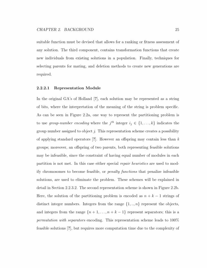
2.2.2.1 Representation Module
In the original GA’s of Holland [?], each solution may be represented as a string
of bits, where the interpretation of the meaning of the string is problem specific.
As can be seen in Figure 2.2a, one way to represent the partitioning problem is
to use group-number encoding where the j th integer ij ∈ {1, . . . , k} indicates the
group number assigned to object j. This representation scheme creates a possibility
of applying standard operators [?]. However an offspring may contain less than k
groups; moreover, an offspring of two parents, both representing feasible solutions
may be infeasible, since the constraint of having equal number of modules in each
partition is not met. In this case either special repair heuristics are used to mod-
ify chromosomes to become feasible, or penalty functions that penalize infeasible
solutions, are used to eliminate the problem. These schemes will be explained in
detail in Section 2.2.3.2. The second representation scheme is shown in Figure 2.2b.
Here, the solution of the partitioning problem is encoded as n + k − 1 strings of
distinct integer numbers. Integers from the range {1, .., n} represent the objects,
and integers from the range {n + 1, . . . , n + k − 1} represent separators; this is a
permutation with separators encoding. This representation scheme leads to 100%
feasible solutions [?], but requires more computation time due to the complexity of

CHAPTER 2. BACKGROUND 26
M7M6M5M3M8M4M2M1
BLOCK 1BLOCK 0
(b) Permutation with Separator Encoding.
(a) Group Number Encoding
01110100
M8M7M6M5M4M3M2M1
Figure 2.2: Representation schemes and genetic operators
the unary operator involved.
2.2.2.2 Evaluation Module
Genetic Algorithms work by assigning a value to each string in the population
according to a problem-specific fitness function. It is worth noting that nowhere
except in the evaluation function is there any information (in the Genetic Algo-
rithm) about the problem to be solved. For the circuit partitioning problem, the
evaluation function measures the worth (number of cuts) of any chromosome (par-
tition) for the circuit to be solved and this is the most time consuming function for
this problem.
2.2.2.3 Reproduction Module
This module is perhaps the most significant component in the Genetic Algorithm.
Operators in the reproduction module, mimic the biological evolution process, by

CHAPTER 2. BACKGROUND 27
using unary (mutation type) and higher order (crossover type) transformation to
create new individuals. Mutation as shown in Figure 2.3c is simply the introduction
of a random element, that creates new individuals by a small change in a single
individual. When mutation is applied to a bit string, it sweeps down the list of bits,
replacing each by a randomly selected bit, if a probability test is passed. On the
other hand, crossover recombines the genetic material in two parent chromosomes
to make two children. It is the structured yet random way that information from
a pair of strings is combined to form an offspring.
Crossover begins by randomly choosing a cut point K where 1 ≤ K ≤ L, and L is
the string length. The parent strings are both bisected so that the leftmost partition
contains K string elements, and the rightmost partition contains L − K elements.
The child string is formed by copying the rightmost partition from parent P1 and
then the leftmost partition from parent P2. Figure 2.3 shows an example of applying
the standard crossover operator (sometimes called one-point crossover) to the group
number encoding scheme. Increasing the number of crossover points is known
to be multi-point crossover. The mutation and crossover operators as described
above, apply for the first representation scheme “group number encoding”. These
operators are modified for the “permutation with separator encoding” scheme. A
mutation in this case, would swap two objects (separators excluded). The crossover
operator considered is the partially matched crossover (PMX) [?]. As shown in
Figure 2.3d, PMX builds an offspring by choosing a sub-partition of a solution from
one parent, and preserving the position of as many modules as possible from the
other parent. A sub-partition of the solution is selected by choosing two random cut
points, which serve as boundaries for swapping operations. Figure 2.3e illustrates

CHAPTER 2. BACKGROUND 28
this process in detail. Generally, the results of the Genetic Algorithms based on
permutation with separators encoding are better than those based on group-number
encoding, but take a longer time to converge [?].
2.2.2.4 Population Module
This module contains techniques for population initialization, generation replace-
ment, and parent selection techniques. The initialization techniques generally used
are based on pseudo-random methods. The algorithm will create its starting pop-
ulation by filling it with pseudo-randomly generated bit strings.
Strings are selected for mating based on their fitness, those with greater fit-
ness are awarded more offspring than those with lesser fitness. Parent selection
techniques that are used, vary from stochastic to deterministic methods. The prob-
ability that a string i is selected for mating is pi, the ratio of the fitness of string
i to the sum of all string fitness values, pi = fitnessi∑
jfitnessj
. The ratio of individual
fitness to the fitness sum denotes a ranking of that string in the population. The
Roulette Wheel Selection method is conceptually the simplest stochastic selection
technique used. The ratio pi is used to construct a weighted roulette wheel, with
each string occupying an area on the wheel in proportion to this ratio. The wheel
is then employed to determine the string that participates in the reproduction. A
random number generator is invoked to determine the location of the spin on the
roulette wheel. In Deterministic Selection methods, reproduction trials (selection)
are allocated according to the rank of the individual strings in the population rather
than by individual fitness relative to the population average.
Generation replacement techniques are used to select a member of the old pop-

CHAPTER 2. BACKGROUND 29
(c) PMX Operator (for permutation with separators encoding)
Unknown
Mapping
=X
=
STEP4: Use Mapping to fill the rest of PositionsSTEP3: Fill Posistions (no Conflict)
)2843,71
5
56(O2
O1
O2 (
O1 (
O2 (
O1 (
)3618,472(
)2x43,75x6
One point crossover
STEP2: Swap Segments Between Cut Points
)x618,472x
STEP1: Two Cut Points
10-
111
000
111
000
(b) Standard Crossover Operator (for group number encoding)
110Child2:
001Child1:
000Parent1:
11
(a) Standard Mutation Operator
1100
0011
0101
.001.894.473.760
.840.005.096.120
.373.266.102.801
0100
0011
0101
ChromosomeNew
BitNew
NumbersRandom
ChromosomeOld
Parent1: 1
P1 ( 1 2 5 7 , 3 4 6 8 ) x x 7 4 , 8 1 x x )
)xx43,75xx)2318,4756P2 (
Figure 2.3: Genetic Operators

CHAPTER 2. BACKGROUND 30
ulation and replace it with the new offspring. The quality of solutions obtained
depends on the replacement scheme used. Some of the replacement schemes used
are based on: (i) deleting the old population and replacing it with new offsprings
(GA-dop), (ii) replacing parent solutions with sibling (GA-rps), (iii) replacing the
most inferior members (GA-rmi) in a population by new offsprings. Variations to
the second scheme use an incremental replacement approach, where at each step
the new chromosome replaces one randomly selected from those which currently
have a below-average fitness. The quality of solutions improve using the second
replacement scheme. The reason is that this replacement scheme maintains a large
diversity in the population.
2.2.3 GA Implementation
Figure 2.4 shows a simple Genetic Algorithm. The algorithm begins with an encod-
ing and initialization phase during which each string in the population is assigned a
uniformly distributed random point in the solution space. Each iteration of the ge-
netic algorithm begins by evaluating the fitness of the current generation of strings.
A new generation of offspring is created by applying crossover and mutation to pairs
of parents who have been selected based on their fitness. The algorithm terminates
after some fixed number of iterations.
2.2.3.1 Parameters affecting the performance of Genetic Search
Running a Genetic Algorithm entails setting a number of parameter values. Finding
settings that work well on one’s problem is not a trivial task. If poor settings are
used, a Genetic Algorithm’s performance can be severely impacted. Central to

CHAPTER 2. BACKGROUND 31
GENETIC ALGORITHM1. Encode Solution Space2.(a) set pop size, max gen, gen=0;
(b) set cross rate, mutate rate;3. Initialize Population.4. While max gen ≥ gen
Evaluate FitnessFor (i=1 to pop size)Select (mate1,mate2)if (rnd(0,1) ≤ cross rate)child = Crossover(mate1,mate2);
if (rnd(0,1) ≤ mutate rate)child = Mutation();
Repair child if necessaryEnd ForAdd offsprings to New Generation.gen = gen + 1
End While5. Return best chromosomes.
Figure 2.4: A generic Genetic Algorithm
these components are questions pertaining to appropriate representation schemes,
lengths of chromosome strings, optimal population sizes, and frequency with which
the transformation functions are invoked.
Choosing the population size for a Genetic Algorithm is a fundamental decision
faced by all GA users. On the one hand, if too small a population size is selected, the
Genetic Algorithm will converge too quickly to a poor solution. On the other hand,
a population with too many members results in long waiting times for significant
improvement, especially when evaluation of individuals within a population must
be performed wholly or partially in serial. Regarding the reproduction module,
experimental data confirms that mutation rates above 0.04 are generally harmful

CHAPTER 2. BACKGROUND 32
with respect to on-line performance. The absence of mutation is also associated
with poorer performance, which suggests that mutation performs an important
service in refreshing lost values. Good on-line performance is associated with high
crossover rate combined with low mutation rate.
Therefore, GA has many variables associated with its implementation. Many
of the parameters available to a GA are:
1. The initial population members (usually randomly generated),
2. The initial population size,
3. The size of the population members,
4. The population’s encoding scheme,
5. The stopping criterion (e.g. number of generations),
6. The scheme used for selection and replacement of population members,
7. The initial seed for pseudo-random number generator,
8. The mutation and crossover probabilities,
9. The fitness function.
2.2.3.2 Performance of Genetic Algorithm
Two methods for solving the problem of producing infeasible solutions using the Ge-
netic Algorithm were introduced in section 2.2.2.1. The first is based on a penalty
function, where infeasible solutions are penalized such that their fitness is decreased

CHAPTER 2. BACKGROUND 33
according to the deviation from the feasible solution required. The second method
is based on repairing the infeasible solutions produced by crossover and mutation.
To repair a corrupted chromosome, one could either use a simple repair scheme
where extra genes belonging to a certain block are randomly moved to other un-
balanced blocks, or a more efficient repair scheme is used, where genes are moved
to unbalanced blocks such that the gain is increased (cut-net size is decreased).
Many other operators and variations of genetic algorithms exist. Some other
GA operators are:
1. Multi-Point crossover which allows more than two strings to mate and gener-
ate offsprings,
2. Inversion which reverses a substring of a given string,
3. PMX, OX and CX which are permutation crossover operators used in the
travelling salesman problem.
Finally, hybrid schemes can be used to improve GA performance by using the GA
to approach a fit solution but using specialized local optimization methods armed
with problem specific knowledge to arrive at a final solution. Therefore, GA is an
efficient optimization algorithm. It explores to investigate new and unknown areas
in the search space to find global maximum. Genetic Algorithms have been applied
to many areas. Some successful GA applications include VLSI layout optimization,
job shop scheduling, function optimization and the travelling salesman problem
(TSP).

CHAPTER 2. BACKGROUND 34
2.2.4 Mapping Genetic Algorithm to Hardware
The nature of GA operators is such that GAs lends themselves well to pipelining and
parallelization. For example, selection of population members can be parallelized
to the practical limit of area of the chip(s) on which selection modules are imple-
mented. Once these modules have made their selections, they can pass the selected
members to the modules, which perform crossover and mutation, which in turn
pass the new members to the fitness modules for evaluation. Thus a coarse-grained
pipeline is easily implemented. This capability for parallelization and pipelining
helps in mapping GA to hardware.
2.3 Overview of Field Programmable Gate Ar-
rays
Field Programmable Gate Arrays(FPGAs) are an inexpensive user-programmable
device, which allows rapid design prototyping [Brow92]. The user programmability
allows for short time to market of hardware designs. They offer more dense logic
and less tedious wiring work than discrete chip designs and faster turn around than
sea-of-gates, standard cell, or full-custom design fabrication. FPGAs are generally
composed of logic blocks which implement the design’s logic, I/O cells which connect
the logic blocks to the chip pins and interconnection lines which connect logic blocks
together with I/O cells as shown in Figure 2.5.
The input/output blocks (IOBs) provide the interface between the package pins
and internal signal lines. The programmable interconnect resources provide routing

CHAPTER 2. BACKGROUND 35
Figure 2.5: Field Programmable Gate Arrays
paths to connect the inputs and outputs of the Configurable logic blocks (CLBs)
and IOBs onto the appropriate networks. Customized configuration is established
by programming internal static memory cells that determine the logic functions
and internal connections implemented in the FPGA.
Figure 2.6 depicts a FPGA with a two-dimensional array of logic blocks that
can be interconnected by interconnect wires. All internal connections are composed
of metal segments with programmable switching points to implement the desired
routing. An abundance of different routing resources is provided to achieve efficient
automated routing. There are four main types of interconnect, of which three are
distinguished by the relative length of their segments: single-length lines, double-
length lines and Longlines. (NOTE: The number of routing channels shown in the
figure is for illustration purposes only; the actual number of routing channels varies

CHAPTER 2. BACKGROUND 36
Figure 2.6: FPGA with a two dimensional array of logic blocks.
with the array size.) In addition, eight global buffers drive fast, low-skew nets most
often used for clocks or global control signals. The principal CLB elements are
shown in Figure 2.7. Each CLB contains a pair of flip-flops(FF), logic for boolean
functions(H) and two independent 4-input function generators(F,G). These function
generators have a good deal of flexibility as most combinatorial logic functions need
less than four inputs. Configurable Logic Blocks implement most of the logic in
an FPGA. The flexibility and symmetry of the CLB architecture facilitates the
placement and routing of a given application.
Programming of these components is allowed with the use of static RAM cells,
anti-fuses, EPROM transistors or EEPROM transistors.
Xilinx FPGAs use static RAM technology to implement hardware designs. Be-
cause of this they are reprogrammable and frequently used in prototyping and other
areas where reprogrammability is useful. Commonly used Xilinx FPGAs today are
from the Virtex-II Pro family, which is Xilinx’s most advanced line of FPGAs.
Although field programmable gate arrays were introduced a decade ago, they

CHAPTER 2. BACKGROUND 37
Figure 2.7: Configurable Logic Block.
have only recently become more popular. This is not only due to the fact that
programmable logic saves development cost and time over increasingly complex
ASIC designs, but also because the gate count per FPGA chip has reached numbers
that allow for the implementation of more complex applications (e.g. VirtexE,
Virtex-II Pro etc. FPGAs have million of gates).
Many present day applications utilize a processor and other logic on two or more
separate chips. However, with the anticipated ability to build chips with over ten
million transistors, it has become possible to implement a processor within a sea of
programmable logic, all on one chip. Such a design approach allows a great degree
of programmability freedom, both in hardware and in software. CAD tools could
decide which parts of a source code program are actually to be executed in software
and which other parts are to be implemented with hardware. The hardware may be
needed for application interfacing reasons or may simply represent a co-processor
used to improve execution time.
FPGA designs can be created in a number of ways, including graphical schematic

CHAPTER 2. BACKGROUND 38
component layout (Powerview) and hardware description languages such as ABEL,
VHDL, and Verilog. VHDL (VHSIC hardware description language) can be used
either for behavioral modeling of circuit designs or for logic synthesis using either
behavioral or structural descriptions [Skah96], [Yala01], [Bhas99]. Since writing
structural circuit descriptions is like trying to describe a circuit using text instead
of a schematic editor, the real advantage of VHDL is seen only in its behavioral
synthesis potential.
2.4 Overview of Reconfigurable Computing Sys-
tems
Due to its potential to greatly accelerate a wide variety of applications, reconfig-
urable computing has become a subject of a great deal of research. Its key feature
is the ability to perform computations in hardware to increase performance, while
retaining much of the flexibility of a software solution.
Reconfigurable systems [Comp02] are usually formed with a combination of
reconfigurable logic and a general purpose microprocessor. The processor performs
the operations that cannot be done efficiently in reconfigurable logic, while the
computational cores are mapped to reconfigurable hardware. This reconfigurable
logic can be supported by either FPGAs or other custom configurable hardware.
Reconfigurable computing involves manipulation of the logic within the FPGA at
run-time. In other words, the design of the hardware may change in response to
the demands placed upon the system while it is running. Here, the FPGA acts as
an execution engine for a variety of different hardware functions, some executing

CHAPTER 2. BACKGROUND 39
in parallel, others in serial.
The design process in a reconfigurable hardware involves first partitioning the
design into sections to be implemented on hardware and software. The portion of
design which is to be implemented on hardware is synthesized into a gate level or
register transfer level circuit description. This circuit is mapped onto logic blocks
within the reconfigurable hardware during the technology mapping phase. These
mapped blocks are then placed into a specific physical block within the hardware,
and the pieces of the circuit are connected using the reconfigurable routing. After
compilation, the circuit is ready for configuration onto the hardware at run-time.
Nowdays, various tools are available which can automatically compile all these steps
and the designer requires very little effort to use the reconfigurable hardware. The
complete design process is shown in the Figure 2.8.
Reconfigurable architectures [Bond00] have mostly evolved from FPGAs. But
FPGAs use fine grained architectures with pathwidths of 1 bit. These architectures
are much less efficient because of huge routing area overhead and poor routability.
Due to single bit wide configurable logic block, it includes just a few gates. For
function selection it needs 4 or more flip flops with at least 4 gates per flip flop
of configuration RAM. Using FPGA as a computing element several CLBs are
united to form a several bit-wide datapath. Therefore, fine granularity FPGAs use
only about 1% chip area for active logic circuits and about 90% for wiring, from
which major part is used for reconfigurable routing areas. It has shown that on
applications with large data elements, fine grained devices pay much more area
for interconnect than coarse-grained devices which have pathwidths greater than 1
bit. Coarse-grained architectures can be more area efficient. These architectures

CHAPTER 2. BACKGROUND 40
DESIGN SPECIFICATIONS
ALGORITHM DESIGN & ANALYSIS
SYSTEM ARCHITECTURE DESIGN
(HW/SW Partitioning)
HDL CODING
FUNCTIONAL SIMULATION
SYNTHESIS
PLACE/ ROUTE
SW DEVELOPMENT
HW/SW INTEGRATION
DESIGN CONSTRAINTS
HW IP LIBRARY
SW IP LIBRARY
CO-VERIFIVATION
TIMING SIMULATION
Figure 2.8: Design Steps for Reconfigurable Computing.

CHAPTER 2. BACKGROUND 41
provide word level datapaths and powerful and very area-efficient datapath routing
switches. A major benefit is the massive reduction of configuration memory and
configuration time, as well as drastic complexity reduction of the placement and
routing problem. Several architectures are outlined in [RHar97], [Cher94], [RKre95]
Reconfigurable computing has several advantages. First, it is possible to achieve
greater functionality with a simpler hardware design. Because not all of the logic
must be present in the FPGA at all times, the cost of supporting additional features
is reduced to the cost of the memory required to store the logic design.
The second advantage is lower system cost. On a low-volume product, there will
be some production cost savings, which result from the elimination of the expense of
ASIC design and fabrication. However, for higher-volume products, the production
cost of fixed hardware may actually be lower. Systems based on reconfigurable
computing are upgradable in the field. Such changes extend the useful life of the
system, thus reducing lifetime costs.
The final advantage of reconfigurable computing is reduced time-to-market.
There are no chip design and prototyping cycles, which eliminates a large amount
of development effort. In addition, the logic design remains flexible right up until
(and even after) the product ships. Therefore, reconfigurable platforms and their
applications are heading from niche to mainstream, bridging the gap between ASICs
and microprocessors.

CHAPTER 2. BACKGROUND 42
2.5 Previous work in Hardware based GA
The past several years have seen a sharp increase in work with reconfigurable hard-
ware systems. Reconfigurability is essential in a general-purpose GA engine because
certain GA modules require changeability (e.g. the function to be optimized by the
GA). Thus a hardware-based GA is both feasible and desirable. In the present sur-
vey, a set of research papers on hardware implementations of GA have been studied
and analyzed. The results of the analysis are presented here-forth.
2.5.1 Specific Architectures to speed GA
The key to the hardware implementation of the GA is to divide the algorithm into
sub-sections and perform the latter using dedicated hardware modules in parallel.
The various architectures are discussed in the following sections.
2.5.1.1 Splash 2 reconfigurable Computer
In [Paul95], the GA is implemented in hardware on a Splash 2 reconfigurable com-
puter. The problem selected for implementation is the famous Traveling Salesman
Problem. Splash2 is a reconfigurable computer consisting of an interface board and
a collection of processor array boards. Its basic unit of computation is the pro-
cessor, which consists of four Xilinx 4010 FPGA’s and associated memories. The
functions performed by various FPGA’s are as follows:
1. FPGA-1 performs the Roulette Wheel Selection, which involves choosing pairs
from the memory, based upon fitness.
2. FPGA-2 performs the crossover depending upon crossover probability.

CHAPTER 2. BACKGROUND 43
3. FPGA-3 calculates the new fitness of tours formed by crossover and randomly
selects tours for mutation and sends the tour pairs and their fitness to FPGA4.
4. FPGA-4 writes the new population into the memory.
A 4-processor island model of parallel computation is developed for parallelizing
the algorithm, which outperformed the performance of 1-processor, 4-processor
Trivial, and 8-processor trivial architecture [Paul95]. The architecture proposed in
[Paul95] has the following advantages:
1. The individual data objects manipulated by the algorithm are small.
2. The requirements for Splash 2 parallel GA (SPGA) are modest, consisting of
small word addition, subtractions, and comparisons.
3. The additional work required to create parallel implementations of the algo-
rithm is minimal.
In [Paul96] Paul Graham and Brent Nelson further analyzed the performance dif-
ferences between Hardware and Software versions of Genetic Algorithm in solving
TSP. The hardware implementation consisted of 4 FPGA’s and associated mem-
ories arranged in bi-directional pipeline as explained in [Paul95]. C++ code was
used for software implementation of SPGA and comparisons of two implementa-
tions showed that the hardware performs up to 50 times the work per cycle. The
hardware features responsible for its advantages are:
1. Hard-wired control
2. Memory hierarchy efficiency

CHAPTER 2. BACKGROUND 44
3. Parallelism
The factors having the most effect on the improved hardware performance are as
follows:
1. Parallel execution of selection operation used in the hardware implementa-
tions as opposed to a serial selection in software version.
2. Address instructions, branching instructions introduce a lot of overhead in
software implementation. In hardware, this overhead is eliminated by use of
dedicated state machines and address counters.
3. Parallelism in performing the crossover and mutation operations results in a
1.5 to 2 times increase in performance for hardware.
4. A little bit of the performance increase comes as a result of faster generation
of random numbers in the hardware implementation.
2.5.1.2 The Xilinx XC6216
The Xilinx XC6216 was used to accelerate the GA performance in [Koza97]. It
accelerated the most time-consuming fitness task of GA by embodying each indi-
vidual of evolving population into hardware. A 16 step-sorting network for seven
items was evolved using XC6216 in which sequence of comparison exchange opera-
tors were executed in fixed order. FPGA was used for fitness measurement task and
the host computer performed all the tasks. The use of Xilinx XC6216 has several
advantages over previously available FPGA’s for fitness measurement task of GA.
They are:

CHAPTER 2. BACKGROUND 45
1. It streamlines the downloading task because of the configuration bits in the
address space of host processor.
2. Encoding scheme for configuration bits is public.
3. Encoding Scheme for configuration bits is simple thereby accelerating the
technology mapping, placement, routing, and bit creation tasks.
4. It is invulnerable to damage. Most FPGAs are vulnerable to damage caused
by combinations of configurations bits that connect contending digital signals
to the same line. Invulnerability to damage is needed in order to make FPGAs
practical for inner loop of the genetic algorithm.
Therefore, this research demonstrated how massive parallelism of rapidly recon-
figurable Xilinx XC6216 FPGA can be exploited to accelerate the computationally
bundersome task of fitness calculation of genetic programming.
2.5.1.3 ARMSTRONG III-The MIMD Multicomputer
Complex and expensive hardware is employed to attain the speedups. For exam-
ple, SPLASH2 uses a collection of processor array boards connected to Sun Spark
workstation via an interface card [Paul95]. Another example is the ARMSTRONG,
which is a MIMD (Multiple Instruction Multiple Data) multicomputer with recon-
figurable resources [Sitc]. It consists of an array of processor boards. Each board
consists of microprocessor, memory, and FPGAs. These machines are regarded as
reconfigurable computers, developed for general computation. The implementa-
tion still suffers from memory latency limiting the operating clock frequency. The
CHAPTER 2. BACKGROUND 46
memory bottleneck is inevitable since GA requires a large memory to store the
population. As a result, high-speed memory may be used making the hardware ex-
pensive or low-cost memory reducing performance. The purpose of Armstrong III
projects is to show that an architecture consisting of a small set of reconfigurable
resources augmenting a host microprocessor has real advantages. In particular, it
has been shown that this architecture is well-suited for computationally intensive
algorithms. The results show that Armstrong III node can perform three times
faster than a 60 Mhz workstation.
2.5.1.4 Compact GA
In contrast to the Simple GA, the Compact GA is more suitable for hardware imple-
mentation [Chat01]. The Compact GA represents a population as an L-dimensional
vector, where L is the chromosome length. Thus the compact GA manipulates this
vector instead of the actual population. This dramatically reduces a number of bits
required to store the population. With this representation, it is practical to use
registers for a probability vector. The Compact GA executes one generation per
three clock cycles for one-max problem. So design, though simple, runs about 1000
times faster than the software executing on a workstation. The compact GA theo-
retically simulates the oder-one behaviour of Simple GA using binary tournament
selection and uniform crossover. Therefore the Compact GA cannot absolutely
replace Simple GA for all classes of problems.

CHAPTER 2. BACKGROUND 47
2.5.1.5 Systolic Architectures
Though FPGA’s helped in solving the implementation issues associated with spe-
cial purpose systems but the costs associated with designing such systems are still
significant. So design of systolic architecture was proposed in [IMBla] as a means
of mitigating the costs. Systolic Array is an arrangement of processors in an array
(often rectangular) where data flows synchronously across the array between neigh-
bours, usually with different data flowing in different directions. Each processor at
each step takes in data from one or more neighbours (e.g. North and West), pro-
cesses it and, in the next step, outputs results in the opposite direction (South and
East). Special appeal of systolic arrays is that they can be derived mechanically
by provably correct and (in a sense) optimal synthesis methods. These methods
transform algorithmic descriptions that do not specify concurrency or commmuni-
cation, usually functional or imperative programs, into functions that distribute the
program’s operations over time and space. This process is called systolic design.
The distribution functions can then be refined further and translated into a de-
scription for fabrication of a VLSI chip or into a distributed program for execution
on a programmable processor array. Also there were many advantages of using this
approach:
1. Architectures are modular and expandable.
2. Design route is fast and manageable.
3. Large or small instantiations of a particular design can be implemented by
reconfiguring the FPGA.

CHAPTER 2. BACKGROUND 48
4. The design is massively parallel and significant throughput can be achieved.
In this design four systolic arrays formed a macro-pipeline, which were used
to implement the operators. But the design does not concentrate on the fitness
function calculation, which in general proves to take the majority of time.
In [IMBlb] a parallel hardware random number generator for use with a VLSI
genetic algorithm-processing device was proposed. The design uses a systolic array
of mixed congruential random number generators. The generators are constantly
re-seeded with the outputs of the proceeding generators to avoid significant biasing
of the randomness of the array, which would result in longer times for the algorithm
to converge to the solution. The design uses a number of custom systolic arrays
to achieve the selection and reproduction of a population of chromosomes. The
advantages of using the design are:
1. Massive parallelism
2. Data re-use
3. Uni-directional data flow between cells
4. Preserves independence of random sequences generated by re-seeding each
element with the output of each element after each number has been produced.
2.5.1.6 PAM (Programmable Active Memory) Architecture
Bertin et.al. [PBer93] worked with a programmable active memory (PAM) archi-
tecture which composed of a 55 array of Xilinx XC3090 FPGAs and supporting

CHAPTER 2. BACKGROUND 49
hardware, all combined to act as a co-processor to a host system. Compiling and
running an application on PAM architecture consisted of:
1. Identifying the critical computations best suited for hardware implementa-
tions.
2. Implementing and optimizing the hardware part on the PAM.
3. Implementing and optimizing the software part on the host system.
After testing on different applications it was found that the performance of PAM
implementation was competitive with supercomputer implementation of the same
application but was upto 100 times cheaper in dollars per operation per second.
But many complex applications are beyond the reach of current PAM technology.
2.5.1.7 Other Reconfigurable Architectures
In evolutionary computation, evolutionary operations are applied to a large number
of individuals (genes) repeatedly. The computation can be pipelined (evolutionary
operators) and parallelized ( a large number of individuals) by dedicated hardware,
and high performance is expected. However, details of the operators depend on
given problems and vary considerably. Systems with Field Programmable Gate
Arrays can be reconfigured and realize the most suitable circuits for given prob-
lems. In [Maru00], it was shown that a co-processor system with a Virtex FPGA
can achieve high performance in evolutionary computations by utilizing the two fea-
tures of FPGA. First, agents in evolutionary computation models which are usually
expressed using short bit-strings can be stored in distributed select RAMs of Virtex
CHAPTER 2. BACKGROUND 50
FPGAs very efficiently. Second, the partial reconfiguration and readback functions
of the FPGAs make it possible to exploit parallelism without thinking about cir-
cuits for data I/O. Gokhale [MGok91] developed a programmable linear logic array
called SPLASH that was applied to many areas, including one-dimensional pattern
matching between DNA sequence and a library sequences. Splash greatly outper-
formed several more expensive alternatives, including the P-NAC, a CM-2 and a
Cray-2. It consisted of 32 Xilinx XC3090 and 32 memory chip. Also in [Maru01],
it was shown that a hardware system with two FPGAs and SRAMs, achieved 50
times of speedup compared with a workstation (200MHz) in some evolutionary
computation problems.
The use of reconfigurable hardware for the design of GA was also seen in projects
such as [Scot94], [Rint00], [Wirb84]. In Stephan Scott’s behavioral-level implemen-
tation of a GA [Scot94], the targeted application was optimization of an input
function. In [Rint00], a GA was designed and implemented on a PLD, using Al-
tera hardware description language(AHDL). In [Wirb84], a number of GAs were
designed and implemented in a text compression chip.
2.6 Summary
In this chapter, it is concluded from the literature that hardware GA yields a signif-
icant speedup over software GA due to pipelining, parallelization and no function
call overhead. This is useful when GA is used for real-time applications. Thus
a hardware implementation exploits the reprogrammability of FPGA’s, which are
programmed via a bit pattern stored in a static RAM and are thus easily reconfig-

CHAPTER 2. BACKGROUND 51
ured.
Genetic Algorithms have been applied to many areas. Some successful GA appli-
cations include VLSI layout optimization, function optimization and the travelling
salesman problem (TSP). In the next chapter, the architecture used for mapping
genetic algorithms into hardware for circuit partitioning is explained.

Chapter 3
Architecture
This chapter describes an architecture of a genetic algorithm processor along with
the functional description of each module. The design is used to solve the problem of
circuit-partitioning. The representation used to solve circuit-partitioning problem
is also described. The VHDL code for top-level file and testbench for the design is
given in Appendix C and the code for other modules explained in this chapter is in
[?].
3.1 System Specifications and Constraints
The GA Processor proposed in this research, was designed as per the following
system specifications and constraints.
1. One of the main goals of the hardware based GA is to reduce the processing
time as compared to the software implementations. In [Scot94], a hardware
design for the GA is proposed which can be implemented on a single FPGA.
52

CHAPTER 3. ARCHITECTURE 53
The processing time for this hardware implementation is approximately 3-4
times less than the time taken by the software implementation. The architec-
ture proposed in this research should be able to reduce the processing time
by at-least the same factor. The improvement in processing speed acheived
by the proposed architecture is provided in Section 3.8.
2. An equally important contraint for the hardware implementation is the amount
of hardware resources needed. Although there are architectures available in
literature which use multiple FPGA’s to perform the different GA operations
in parallel, such a hardware solution may become too costly, and hence much
less practical to use. The architecture proposed in this research should be im-
plemented on a single FPGA, thus reducing the hardware resources needed.
In order to further minimize the hardware resources, the area/gate utilization
of the FPGA should be as small as possible. This would enable the imple-
mentation to be performed on a small-sized FPGA or additional blocks to be
implemented on the same large-sized FPGA.
3. The design should be easily configured for different sized problems during
synthesis. This ensures that the same RTL code can be used for a wide
range of applications, thus making it easier for portability. In RTL code, this
can be acheived by using generics or parameters, of which the hardware can
be changed based upon the size of the application. These generics can be
changed at the time of digital synthesis. The generics used in the proposed
design are given in Table 3.2.
4. The design should be modular. This means that the design should be split

CHAPTER 3. ARCHITECTURE 54
up into smaller modules, each designed to perform a well defined and well-
partitioned function. This makes the design easier to debug, understand, and
also helps in the design-reuse methodology such as a local search accelerator
can be integrated with it in the future to act as a memetic processor.
5. The design should have control registers with simple read/write interface for
changing operational parameters during run-time. The parameters that can
be changed for different problem-sets are population size, generation count,
number of modules in the netlist, number of nets in the netlist, crossover rate,
and mutation rate. In order to solve problems with large number of nets and
modules, the registers for number of nets and modules are each chosen to
be 16-bit wide. This allows support for problems with number of nets and
modules, each less than or equal to 65536. All other registers are chosen to
be 8-bit wide. This allows population size and generation count to be less
or equal to 256, and crossover and mutation rates to vary between 0 and
255/256, with any increments of 1/256. Details about the control registers
are provided in Section 3.2.1.1.
6. In order to store the input netlist and intermediate populations, memory
blocks have to be used. These memory blocks should be external to the core
(main proposed architecture), and can be implemented either as on-board
memory chips, or block-RAMs that are available on the FPGA. As explained
in Section 3.3, each chromosome and each net is represented using the number
of bits which is equal to the number of modules. Since the number of modules
can be as high as 65536, each chromosome and net-representations have to
CHAPTER 3. ARCHITECTURE 55
be split into memory words, widths of which are determined by the data-bus
widths of the available memory blocks. Although, this results in a much more
complex architecture, it allows the design to solve large problems while taking
into account the practical limitations of memory blocks.
7. The concept of this architecture can be extended to hardware-software co-
design approach by utilizing an ARM processor with an FPGA module.
Therefore, this design is implemented on RPP, which has VirtexE xcv2000E,
FPGA on it.
8. The fitness function is the most time consuming operation in GA, therefore
it should be implemented in hardware.
3.2 System Architecture
The architecture for the GA processor is designed by identifying the various steps
used in the GA and finding a mapping for each of these steps in hardware. The
comparison between the software steps and the equivalent hardware steps followed
in this research are shown in Figure 3.1.
The proposed architecture (core) for implementing the genetic algorithm in
hardware uses a processing-pipeline for performing the computationally extensive
parts of the algorithm. The current design is specifically optimized towards solving
the circuit-partitioning problem.
The design partitioning is performed in such a way that each block performs
a well-defined function, thus making it easier to re-use some of the blocks for a

CHAPTER 3. ARCHITECTURE 56
Initialize the GA parameters
Create Initial Population and
calculate Fitness
Select two parents
Perform Crossover and
Mutation
Replace initial population with the
new population
End of Population?
End of Generation Count?
Output the final population and
final fitness
Yes
No
Yes
No
Loads GA parameters in GA Processor
Loads the netlist data to the GA Processor
GA Processor generates the random initial population and loads them into the Parent Address Space of Chromosome Memory
Fitness module in GA Processor calculates the fitness of Parent chromosomes and
loads the fitness memory
Selection module in GA Processor performs Tournament Selection and generates addresses of two parents
Crossover/Mutation module generates two offsprings using the selected parents and stores them into Child
Address Space of Chromosome Memory
Population Count Done?
Swap the Parent and Child Address Spaces
Generation Count Done?
Fitness module in GA Processor calculates the fitness of Parent chromosomes and
loads the fitness memory
GA Processor outputs the final chromosomes with the corresponding
fitness values
Read netlist from benchmark data
HARDWARE IMPLEMENTATION
SOFTWARE IMPLEMENTATION
No
No
Yes
Yes
Figure 3.1: Hardware software Design Comparison.

CHAPTER 3. ARCHITECTURE 57
different type of optimization problem. A common controller approach is followed
in which a central main controller generates the control signals for all the other
blocks in the design. Separate blocks are used to perform the selection, crossover
and mutation, and fitness calculation. The main controller is used to schedule the
operations of these blocks using an “enable/disable” signal for each block. Each
block notifies the main controller when the task is completed using a “done” signal.
Please note that contrary to some of the architectures proposed in the past, the
fitness module is also implemented in hardware. Since fitness calculation is the
most time consuming operation in the GA, the added complexity arising from the
hardware implementation of fitness is out-weighed by the improvement in processing
speed acheived over the software implementation of fitness calculation.
The design waits for an active high pulse on the “StartGA” input before per-
forming any computations. After receiving a “StartGA” pulse, the main con-
troller generates a random initial population and stores it into the chromosome
memory (Section 3.2.3). Following this, the main controller enables the selection,
crossover/mutation, and fitness modules in sequence, until all the generations are
complete. When all the generations are processed, the main controller outputs the
chromosomes with the corresponding fitness values for the final population. Af-
ter all the results are generated by the core, an active high pulse on the output
“GADone” is generated by the core, signalling the end of processing for the corre-
sponding problem. Since different blocks share the accesses to the same memories,
a memory-mux is used to multiplex the memory-accesses from different blocks. In
addition to these, the control registers are implemented as an independent block.
These registers are accessible through the simple CPU interface (Section 3.2.1.1).
CHAPTER 3. ARCHITECTURE 58
In order to make the implementation easier, the memory blocks required by
the core are implemented as block-RAMs on the xcv2000E FPGA. If the data-
bus widths of the memory blocks are increased (based upon the generic input),
the processing time is reduced. This is because the core is able to process wider
data-words in parallel. However, if the data-widths of block-RAMs are increased,
the address-bus widths are decreased, thus limiting the size of the problems that
can be solved. This reduction in the address-bus width as a result of increase
in the data-bus width, is characteristic to the block-RAM instantiation in Xilinx
FPGA’s. Therefore, there has to be a trade-off between the increase in processing
speed and the size of problem that can be solved by the GA processor. During
implementation, the block-RAMs are chosen to have 8-bit wide data-bus. This is
due to the relatively small size of benchmarks, increasing the data-bus widths to
16-bits does not have a big impact to the processing speed.
Theoretically, there is no limit on the size of the problem the core can handle,
but since the core requires external RAM for storing the netlist information, the
size of the RAM is directly proportional to the product of number of nets and cells
(modules) in the design. Too big problems would require a correspondingly large
amount of external RAM.
3.2.1 Detailed Internal Architecture
The block diagram of the GA processor is shown in Figure 3.2. The selection
module selects the parents with good fitness from Fitness memory and sends the
addresses of the parents selected to Crossover and Mutation module. The Crossover
and Mutation module performs crossover and mutation on the parents. The Fitness

CHAPTER 3. ARCHITECTURE 59
Module generates fitness values for each of the generated chromosomes. The Main
Controller generates control signals for all the blocks,
Figure 3.2: Architecture for the Genetic Algorithm Processor.
meanwhile the Control Registers have to be loaded with ‘legal’ values using the
CPU interface. After loading the control registers, an active high pulse on the Start
control input starts the GA process.
After receiving the Start signaling, the core accepts the netlist from the top-
level inputs. The input netlist is stored in the Netlist memory, from where it is
read repeatedly by the core to compute the fitness. After receiving the input netlist
(based upon the number of nets stored in Control Registers), the core generates the
initial population randomly and stores it into the Chromosome memory. The Selec-
tion module uses Tournament Selection to select two parents. Memory addresses of
these two parents are used by the Crossover and Mutation module to perform the
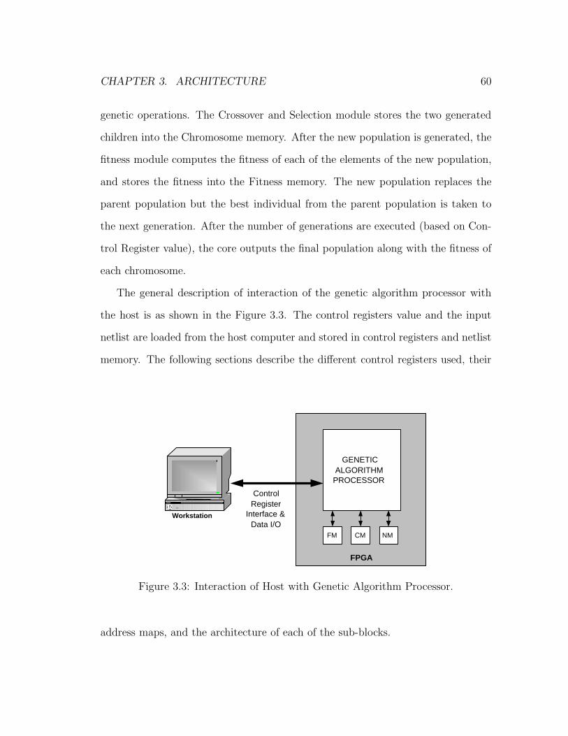
CHAPTER 3. ARCHITECTURE 60
genetic operations. The Crossover and Selection module stores the two generated
children into the Chromosome memory. After the new population is generated, the
fitness module computes the fitness of each of the elements of the new population,
and stores the fitness into the Fitness memory. The new population replaces the
parent population but the best individual from the parent population is taken to
the next generation. After the number of generations are executed (based on Con-
trol Register value), the core outputs the final population along with the fitness of
each chromosome.
The general description of interaction of the genetic algorithm processor with
the host is as shown in the Figure 3.3. The control registers value and the input
netlist are loaded from the host computer and stored in control registers and netlist
memory. The following sections describe the different control registers used, their
Workstation
GENETIC ALGORITHM
PROCESSOR
FM CM NM
Control Register
Interface & Data I/O
FPGA
Figure 3.3: Interaction of Host with Genetic Algorithm Processor.
address maps, and the architecture of each of the sub-blocks.

CHAPTER 3. ARCHITECTURE 61
3.2.1.1 Control Registers
The core uses a set of control registers, which can be programmed using the CPU
interface. The register address map is provided in Table 3.1.
Table 3.1: Register address map
Address Register Size Description
0x00-0x01 CMLength 2x8 Chromosome Length0x02-0x03 NetNum 2x8 Number of nets0x04 PopSiz 1x8 Population size0x05 Gen Num 1x8 Generation Count0x06 CrossoverRate 1x8 Crossover rate0x07 MutationRate 1x8 Mutation rate
1. CMLength Register
Description: This register stores the chromosome length in terms of number
D7 D6 D5 D4 D3 D2 D1 D0
CMLength
CMLength
D15 D14 D13 D12 D11 D10 D9 D8
Figure 3.4: CMlength Register
of Chromosome memory data words CMDataWidth.
Address: 0x00-0x01
Reset Value: 0x0000
Access: Write
2. NetNum Register
Description: This register stores the number of nets in terms of Netlist
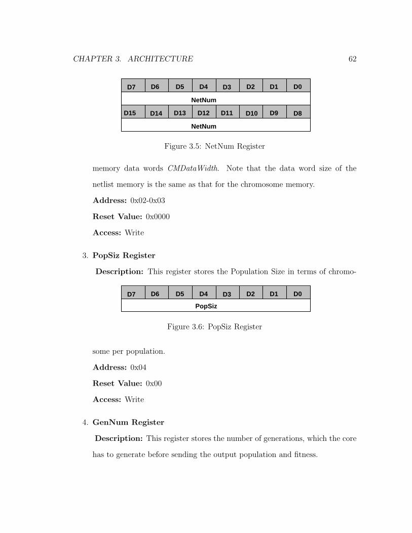
CHAPTER 3. ARCHITECTURE 62
D7 D6 D5 D4 D3 D2 D1 D0
NetNum
NetNum
D15 D14 D13 D12 D11 D10 D9 D8
Figure 3.5: NetNum Register
memory data words CMDataWidth. Note that the data word size of the
netlist memory is the same as that for the chromosome memory.
Address: 0x02-0x03
Reset Value: 0x0000
Access: Write
3. PopSiz Register
Description: This register stores the Population Size in terms of chromo-
D7 D6 D5 D4 D3 D2 D1 D0
PopSiz
Figure 3.6: PopSiz Register
some per population.
Address: 0x04
Reset Value: 0x00
Access: Write
4. GenNum Register
Description: This register stores the number of generations, which the core
has to generate before sending the output population and fitness.

CHAPTER 3. ARCHITECTURE 63
D7 D6 D5 D4 D3 D2 D1 D0
GenNum Not Used
Figure 3.7: GenNum Register
Address: 0x05
Reset Value: 0x00
Access: Write
5. CrossoverRate Register
Description: This register stores the Crossover rate ranging from 0 to 255.
D7 D6 D5 D4 D3 D2 D1 D0
CrossoverRate
Figure 3.8: CrossoverRate Register
Percentage crossover rate is obtained by dividing this register value by 255.
Therefore, 0 represents 0 percentage, and 255 represents 100 percent crossover
rate.
Address: 0x06
Reset Value: 0x00
Access: Write
6. MutationRate Register
Description: This register stores the Mutation rate ranging from 0 to 255.
Percentage Mutation rate is obtained by dividing this register value by 255.
Therefore, 0 represents 0 percentage, and 255 represents 100 percent Mutation
rate.

CHAPTER 3. ARCHITECTURE 64
D7 D6 D5 D4 D3 D2 D1 D0
Mutation Rate
Figure 3.9: MutationRate Register
Address: 0x07
Reset Value: 0x00
Access: Write
3.2.2 Core Generics
The design is coded in VHDL and uses the generics shown in Table 3.2. These
generics helped in making general models instead of making specific models for
many different configurations of inputs and outputs. Generics pass the information
into a design description from its enviornment and helps to reconfigure. Therefore,
testing can be done with different sets of data(different benchmarks).
Table 3.2: Generics used in the design
Generic Name Description Default
FMAddrWidth Fitness memory address width. 9This gives two times maximumsize supported.
FMDataWidth Fitness memory data width. 8CMDataWidth Chromosome memory data width. 8
This represents word size ofchromosome memory.
CMField Number of bits used to represent 8the length of chromosome.
MaxNetNumBits Number of bits used to represent 8maximum number of nets.

CHAPTER 3. ARCHITECTURE 65
3.2.3 Core Memories
The external RAM modules used by the core are listed in Table 3.3. The netlist
memory stores the input netlist, chromosome memory stores the randomly gener-
ated chromosomes for parent and child population and fitness memory stores fitness
of parent and child population.
Table 3.3: Core Memories
Memory Size Description
Netlist 2(MaxNetNumBits+CMField) It stores a binary sequence of length ofMemory ×CMDataWidth chromosome for each net. Each bit in the
sequence denotes if that net is connectedto corresponding cell in the netlist or not.This is single address port synchronousRAM.
Chromosome 2(FMAddrWidth+CMField+1) It stores population elements for theMemory ×CMDataWidth parent as well as child population. The
address space is divided into two halves.Each half stores either parent or childpopulation. This is dual address portsynchronous RAM.
Fitness 2(FMAddrWidth+1) It stores fitness of parent and childMemory ×CMDataWidth population. This is also divided into
two parts for storing parent and childpopulation. This is single addressport synchronous RAM.

CHAPTER 3. ARCHITECTURE 66
3.2.4 Pin Description
The pin description of top level GA processor is described in Table 3.4 and Table 3.5
and shown in Figure 3.10. It describes all the top level inputs and outputs of the
GA Processor.
Clk
ResetN
StartGA
NetlistVld
NetlistIn
PopOut
PopOutVld
FitnessOut
GADone
CP
UA
dd
r
CP
UD
ata
CP
UW
r
NM
Ad
dr
NM
Dat
aRd
NM
Dat
awr
NM
Rd
En
b
NM
WrE
nb
CM
Ad
drR
d
CM
Ad
drW
r
CM
Dat
aRd
CM
Dat
aWr
CM
Rd
En
b
CM
WrE
nb
FM
Ad
dr
FM
Dat
aRd
FM
Dat
aWr
FM
Rd
En
b
FM
WrE
nb
GENETICALGORITHMPROCESSOR
NetlistMemory
ChromosomeMemory
FitnessMemory
Figure 3.10: Pin description of top level GA Processor

CHAPTER 3. ARCHITECTURE 67
Table 3.4: Pin description of Top level GA processor(part1)
Pin Name Direction Description
Clk Input System ClockResetN Input Active low asynchronous reset
Control Register Interface
CPUWr Input Control Register write enableCPUAddr[3:0] Input Control register address busCPUData[7:0] Input Control register data bus
Top-level control and data interface signals
StartGA Input Active high input signal to start GANetlistVld Input Active high control input indicating
that input data NetlistIn is valid.NetlistIn Input Input netlist in words. For eachCMDataWidth-1:0 net, the netlist contains a sequence of
1’s and 0’s which is of size of a chromosome.PopOut Output Final generated population elementsCMDataWidth-1:0 in form of words.PopOutVld Output Output control signal indicating that
PopOut and FitnessOut are valid.FitnessOut Output Output fitness of each outputFMDataWidth-1:0 chromosome.GADone Output Active high pulse indicating end of GA
Chromosome Memory Interface
CMAddrRd Output Chromosome memory read address busFMAddrWidth+CMField-1:0CMDataRd Input Chromosome memory read data busCMDataWidth-1:0CMRdEnb Output Active high read enable for the
Chromosome memoryCMAddrWd Output Chromosome memory write address busFMAddrWidth+CMField-1:0CMDataWr Output Chromosome memory write data busCMDataWidth-1:0CMWrEnb Output Active high write enable for the
Chromosome memory

CHAPTER 3. ARCHITECTURE 68
Table 3.5: Pin description of Top level GA processor(part2)
Pin Name Direction Description
Netlist Memory Read Interface
NMAddr Output Netlist memory address busFMAddrWidth+CMField-1:0NMDataRd Input Netlist memory read data busCMDataWidth-1:0NMRdEnb Output Active high read enable for the
Netlist memoryNMDataWr Output Netlist memory write data busCMDataWidth-1:0NMWrEnb Output Active high write enable for the
Netlist memory
Fitness Memory Write Interface
FMAddr Output Fitness memory address busFMAddrWidth-1:0FMDataRd Input Fitness memory read data busFMDataWidth-1:0FMRdEnb Output Active high read enable for the
Fitness memoryFMDataWr Output Fitness memory write data busFMDataWidth-1:0FMWrEnb Output Active high write enable for the
Fitness memory

CHAPTER 3. ARCHITECTURE 69
3.3 Representation for Circuit-Partitioning
In order to solve the circuit-partitioning problem using GA, the following repre-
sentation is used. Each chromosome contains a sequence of 1’s and 0’s, each bit
corresponding to a distinct cell in the netlist. A ‘1’ at a location in the sequence
means that the corresponding cell lies in the partition number 1. Similarly, a ‘0’
implies that the cell is present in the partition number 0 as shown in Figure 3.11.
Therefore, the length of the chromosome is the number of modules in the circuit.
1 1 1 1 0 0 0
M0 M1 M2 M3 M6 M4 M5 M7
PARTITION 0
NET 1
0 1 0 1 1 1 0 0
0 CHROMOSOME
REPRESENTATION
NET 1 REPRESENTATION
M0 M1 M2 M3 M4 M5 M6 M7
PARTITION 1
Figure 3.11: Representation of chromosome and netlist for circuit-partitioning.
Since there are practical limitations to word sizes of physical memories, the chro-
mosome is stored in the memory in the form of smaller words, words corresponding
to one chromosome being stored consecutively. The netlist is stored into the netlist
memory in a similiar manner. Each net in the netlist has an entry in the netlist
memory which is as wide as the number of modules. For each net, 1’s are placed
in the bit positions corresponding to the modules to which the net is connected
as shown in Figure 3.11. A detailed description of how the proposed netlist and
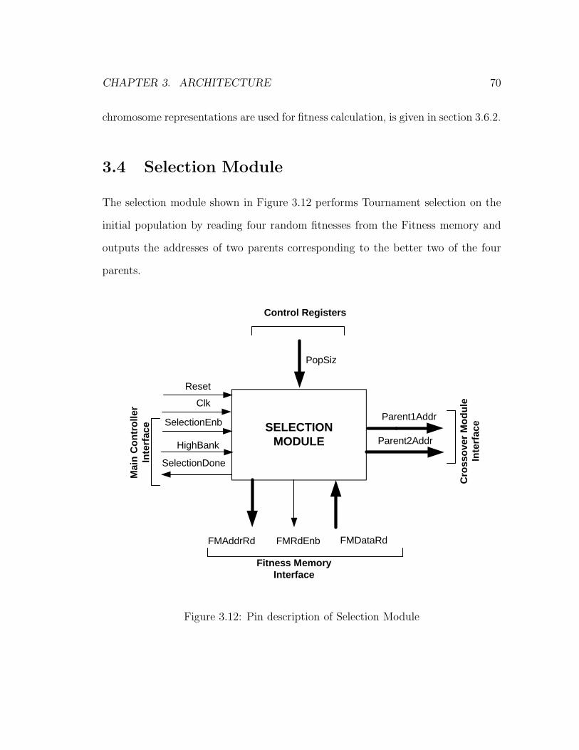
CHAPTER 3. ARCHITECTURE 70
chromosome representations are used for fitness calculation, is given in section 3.6.2.
3.4 Selection Module
The selection module shown in Figure 3.12 performs Tournament selection on the
initial population by reading four random fitnesses from the Fitness memory and
outputs the addresses of two parents corresponding to the better two of the four
parents.
SELECTIONMODULE
SelectionEnb
HighBank
Reset
ClkParent1Addr
Parent2Addr
FMDataRdFMRdEnbFMAddrRd
PopSiz
Fitness MemoryInterface
Cro
sso
ver
Mo
du
leIn
terf
ace
Control Registers
Mai
n C
on
tro
ller
Inte
rfac
e
SelectionDone
Figure 3.12: Pin description of Selection Module

CHAPTER 3. ARCHITECTURE 71
3.4.1 Pin Description
Pin diagram and pin description of Selection Module are shown in Figure 3.12 and
Table 3.6.
3.4.2 Functional Description
The Selection module upon receiving an active high SelectionEnb signal from Main
Controller performs the following functions:
1. Generates four random addresses for the fitness memory and reads four fitness
values from either the low or high memory bank indicated by the HighBank
signal. The selection module uses an instantiation of an LFSR based Random
Number Generator [IMBlb].
2. The Selection Module compares two pairs of fitnesses and selects the best
from each pair.
3. The addresses of the best two fitnesses are latched and held stable on the out-
put signals Parent1Addr and Parent2Addr until the next time when selection
module is enabled.
4. These two addresses (with zeros padded in LSB’s) represent the starting ad-
dresses of the two-parent chromosome stored in the Chromosome memory.
5. At the end of selection of two parents, the selection module generates an
active high pulse on the SelectionDone output signal.

CHAPTER 3. ARCHITECTURE 72
Table 3.6: Pin description of Selection Module
Pin Name Direction Description
Clk Input System ClockResetN Input Active low asynchronous reset
Control Register Interface
PopSiz Input Population size from control registers
Main Controller Interface
SelectionEnb Input Selection enable from main controller(Active high)
SelectionDone Output Selection done signal generated by the selectionmodule signifying the end of selection processfor two parents. (Active high)
HighBank Input Signal from main controller indicating if thethe parent population is stored in the loweror the higher bank in memory. If HighBankhigh, it indicates that the parent population isstored in the second half of the chromosomememory. In this case the children are storedin the first half of the memory.
Crossover Module Interface
Parent1Addr Output Starting address of first selected parent[FMAddrWidth-2:0] chromosome in the Chromosome
memory.Parent2Addr Output Starting address of second selected parent[FMAddrWidth-2:0] chromosome in the Chromosome memory.
Fitness Memory Read Interface
FMAddrRd Output Fitness memory read address bus fromFMAddrWidth-1:0 selection moduleFMDataRd Input Fitness memory read data busFMDataWidth-1:0FMRdEnb Output Active high read enable for the
Fitness memory

CHAPTER 3. ARCHITECTURE 73
Internally, the Selection Module consists of a Random Number Generator, a
Comparator for comparing unsigned integers, registers to latch the generated ran-
dom addresses, and a control state machine as shown in Figure 3.13. The control
state machine generates control/enable signals for different blocks in the module.
The state diagram for the Selection Module is shown in Figure 3.14.
RANDOM NUMBER GENERATOR
ADDRESS REGISTER1
ADDRESS REGISTER2
FITNESS REGISTER1
FITNESS REGISTER2
PARENT REGISTER1
PARENT REGISTER2
SELECTION CONTROL
STATE MACHINE
FITNESS COMPARATOR
FMDataRd
FMAddrRd
FMRdEnb
Parent1Addr Parent2Addr
FITNESS REGISTER DEMUX
ADDRESS SELECTION MUX
PARENT REGISTER DEMUX
ADDRESS REGISTER DEMUX
Main Controller Interface
Control Registers
Figure 3.13: Detailed description of Selection Module.

CHAPTER 3. ARCHITECTURE 74
stIdle
stGenerateAddr1
stGenerateAddr2
stReadFitness1
stReadFitness2
stCompareFitness
stStoreParent
Reset
Parent2Rst = '1'
SelectionEnb = '1'
FMAddrRdInt = Rand;FMRdEnbInt = '1';
GenerateRand = '1';Addr1WrEnb ='1';Addr1In = Rand;
FMAddrRdInt = Rand;FMRdEnbInt = '1';
GenerateRand = '1';Addr2WrEnb ='1';Addr2In = Rand;
Fitness1WrEnb ='1';Fitness1In = FMDataRd;
Fitness2WrEnb ='1';Fitness2In = FMDataRd;
Parent2Set = '1';if(Parent2 ='0') Parent1WrEnb ='1';else Parent2WrEnb='1'endIf(Fitness1LTFitness2) ParentIn = Addr1;else ParentIn = Addr2;
stPreIdle
Parent2 = '1'
Parent2 = '0'
SelectionDoneInt ='1'
Figure 3.14: State Diagram of Selection Module

CHAPTER 3. ARCHITECTURE 75
3.5 Crossover and Mutation Module
The Crossover Module performs the crossover and mutation operations on the two
parent chromosomes, the starting addresses of which are generated by the Selection
Module. The chromosome memory is divided into two parts, namely the low bank,
and the high bank. The parent population is stored into one of the banks and the
child population generated by the crossover and mutation module is stored into the
other bank.
3.5.1 Pin Description
The pin diagram and pin description are shown in Figure 3.15 and Table 3.7.
3.5.2 Functional Description
When an active high pulse on CrossoverEnb input is received, the following func-
tions are performed by the Crossover and Mutation module:
1. One word of the chromosome for each of the parents is read from the Chro-
mosome memory based upon theParent1Addr and Parent2Addr generated
by the Selection Module. After reading one word of chromosome for each
of the parents, the chromosome-word counter is incremented. The Chro-
mosome memory address for each of the parents is generated by appending
the chromosome-word counter value to the Parent1Addr and Parent2Addr as
shown in Figure 3.16.
2. The crossover module generates a random crossover mask for each word of the

CHAPTER 3. ARCHITECTURE 76
Table 3.7: Pin description of Crossover Module
Pin Name Direction Description
Clk Input System ClockResetN Input Active low asynchronous reset
Control Register Interface
CrossoverRate[7:0] Input Crossover RateMutation Rate[7:0] Input Mutation RateCMLength[CMField-1:0] Input Chromosome length
Main Controller Interface
CrossoverEnb Input Crossover enable from main controller(Active high)
CrossoverDone Output Crossover done signal generated by theCrossover and mutation module signifyingthe end of Crossover and mutation process.(Active high)
HighBank Input Signal from main controller indicating if theparent population is stored in the lower orthe higher bank in memory.‘1’ indicates Highbank is used for the parent population.
Selection Module Interface
Parent1Addr Output Starting address of first selected parent[FMAddrWidth-2:0] chromosome in the chromosome
memory.Parent2Addr Output Starting address of second selected parent[FMAddrWidth-2:0] chromosome in the Chromosome memory.
Chromosome Memory Read/Write Interface
CMAddrRd Output Chromosome memory read address busFMAddrWidth+CMField-1:0 from crossover moduleCMDataRd Input Chromosome memory read data busCMDataWidth-1:0CMRdEnb Output Active high read enable for the
Chromosome memoryCMAddrWr Output Chromosome memory write address busFMAddrWidth+CMField-1:0 from crossover moduleCMDataWr Output Chromosome memory write data busCMDataWidth-1:0CMWrEnb Output Active high write enable for the
Chromosome memory

CHAPTER 3. ARCHITECTURE 77
CROSSOVER/MUTATIONMODULE
Clk
CrossoverDone
ChildAddr1
ChildAddr2
CM
Dat
aRd
CM
RdE
nb
CM
Add
rRd
Parent1Addr
Parent2AddrC
MA
ddrW
r
CM
WrE
nb
CM
Dat
aWr
CrossoverRate
MutationRate
CMLength
HighBank
CrossoverEnb
ResetN
Control Registers
Sel
ecti
on
Mo
du
leIn
terf
ace
Chromosome MemoryInterface
Main
Co
ntro
llerIn
terface
Figure 3.15: Pin description of Crossover and Mutation Module
parents. The crossover and mutation rates supplied by the control registers
are compared to an internally generated random number of 8 bits as shown
in Figure 3.17. If the value of this random number is less than the crossover
and mutation rates, these operations are performed, otherwise the parents are
copied to the children. The resulted chromosomes are repaired based upon
the number of cells present in each partition. This is done by reading the
chromosome word-by-word as it is stored in the chromosome memory and
counting the numbers of 1’s and 0’s. A random number is generated which
will select a random bit in a chromosome. The bit is flipped based upon the
difference of number of 1’s and 0’s. The results of the crossover and mutation

CHAPTER 3. ARCHITECTURE 78
Parent1Addr Word Counter
FMAddrWidth-1 bits CMField bits
HighBank
1 bit
Parent2Addr Word Counter HighBank
Figure 3.16: Address generation for the Chromosome Memory.
are stored word-by-word into the Chromosome memory. The starting child
addresses Child1Addr and Child2Addr are obtained from the Main Control
State Machine. Write addresses for the Chromosome memory are generated
in a similar manner as depicted in Figure 3.16, except that the HighBank
is inverted, and Parent1Addr and Parent2Addr are replaced with Child1Addr
and Child2Addr, respectively.
3. Steps 1 and 2 are repeated until the chromosome word counter reaches the
length of the chromosome denoted by the control register CMLength. The sig-
nal CrossoverDone is asserted high signaling the Main Control State Machine
the end of crossover process.
Internally, the crossover module consists of a chromosome word counter, which
is CMField bits wide and trivial combinatorial logic to perform the crossover and
mutation operations as shown in Figure 3.18. Also, the module contains an instan-
tiation of the Random Number Generator. The same random number is used as a
mask for uniform crossover as well as for determining the crossover and mutation
probabilities as shown in Figure 3.17.

CHAPTER 3. ARCHITECTURE 79
DELAY
CROSSOVER LOGIC
MODULE
X-OVER COMPA- RATOR
MUTATION COMPA- RATOR
RANDOM NUMBER
GENERATOR
MUTATION LOGIC
MODULE
MUTATION LOGIC
MODULE
DELAY
MUX
MUX
MUX
MUX
MUX
XoverMask
CMDataRd
MutationRate
CrossoverRate
CMDataWr
MutationMask
Xover- Enable
Mutation- Enable
Child1Word
Child2Word
CHROMOSOME WORD
COUNTER
Parent1Addr
Parent2Addr
Child1Addr
Child2Addr
CMAddrRd
CMAddrWr
Concatenation Operator
Figure 3.17: Detailed Description of Crossover and Mutation Module.
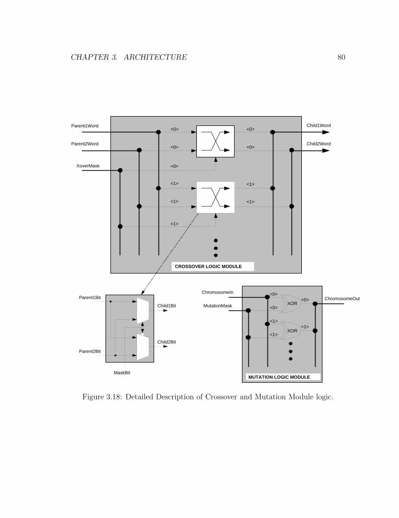
CHAPTER 3. ARCHITECTURE 80
Parent1Word
Parent2Word
XoverMask
Child1Word
Child2Word
<0> <0>
<0> <0>
<0>
<1>
<1>
<1>
<1>
<1>
CROSSOVER LOGIC MODULE
Parent1Bit
Parent2Bit
MaskBit
Child1Bit
Child2Bit
XOR
XOR
MUTATION LOGIC MODULE
ChromosomeIn ChromosomeOut
MutationMask
<1>
<1>
<0>
<1>
<0> <0>
Figure 3.18: Detailed Description of Crossover and Mutation Module logic.

CHAPTER 3. ARCHITECTURE 81
3.6 Fitness Module
The fitness module computes the fitness of the randomly generated population
during initialization. Also, once a complete new population is generated by the
crossover and mutation module, the Fitness module generates fitness values for
each of the generated chromosomes.
3.6.1 Pin Description
The pin diagram of Fitness module is shown in Figure 3.19 and Table 3.8 gives the
pin description.
FITNESSMODULE
HighBankReset
Clk
CM
Dat
aRd
CM
RdE
nb
CM
Add
rRd
NM
Add
rRd
NM
RdE
nb
NM
Dat
aRd
Num
OfN
ets
Psi
ze
Cle
ngth
Control Registers
FitnessEnb
FM
Add
rWr
FM
WrE
nb
FM
Dat
aWr
Fitness MemoryWrite Interface
ChromosomeMemory Read
Interface
Netlist MemoryRead Interface
FitnessDone Main
Co
ntro
llerIn
terface
Figure 3.19: Pin description of Fitness Module

CHAPTER 3. ARCHITECTURE 82
Table 3.8: Pin description of fitness Module
Pin Name Direction Description
Clk Input System ClockResetN Input Active low asynchronous reset
Control Register Interface
NetNum Input Number of nets[MaxNetNumBits-1:0]PopSiz[7:0] Input Population SizeCMLength[CMField-1:0] Input Chromosome length
Main Controller Interface
FitnessEnb Input Fitness enable from main controller(Active high)
FitnessDone Output Fitness done signal generated by theFitness module (Active high)
HighBank Input Signal from main controller indicating ifthe parent population is stored in the loweror the higher bank in memory. ‘1’ indicatesHigh bank is used for the parent population.
Chromosome Memory Read Interface
CMAddrRd Output Chromosome memory read address busFMAddrWidth+CMField-1:0 from crossover moduleCMDataRd Input Chromosome memory read data busCMDataWidth-1:0CMRdEnb Output Active high read enable for the
Chromosome memory
Netlist Memory Read Interface
NMAddr Output Netlist memory address busFMAddrWidth+CMField-1:0NMDataRd Input Netlist memory read data busCMDataWidth-1:0NMRdEnb Output Active high read enable for the
Netlist memory
Fitness Memory Write Interface
FMAddr Output Fitness memory address busFMAddrWidth-1:0 from fitness moduleFMDataWr Output Fitness memory write data busFMDataWidth-1:0FMWrEnb Output Active high write enable for the
Fitness memory
CHAPTER 3. ARCHITECTURE 83
3.6.2 Functional Description
Upon receiving the FitnessEnb signal from the Main Controller, the Fitness module
performs the following functions:
1. For each net, determine if the present chromosome partitioning generates a
cut. For each chromosome the fitness accumulator is reset to 0. The chro-
mosome and the net are read word-by-word from the Chromosome and the
Netlist memory, respectively. For each word of the chromosome and the net,
a simple bit-wise AND operation followed by OR operation is performed as
shown in Figure 3.20.
This generates the information that based upon the present word of chromo-
some, which partition does the net lie in. At any point if the net is found
to be present in a particular partition, the bit representing the presence of
net in that partition is latched, and not overwritten for any subsequent word
operations. At any time, if both of these bits are a ‘1’, that determines a
cut. In this case the fitness accumulator is incremented by one. This pro-
cess is repeated for each word, until the word counter reaches the length of
chromosome.
2. At any time during the computations of a net, if it is found that there is a
cut, no further words are read from the memory. This eliminates the time
wasted by reading redundant information from the Chromosome and Netlist
memories.
3. A chromosome counter keeps track of the number of chromosomes processed.

CHAPTER 3. ARCHITECTURE 84
AND
AND
OR
OR
Latch
Latch
AND
Chromosome
Netlist
Partition 1 Result
Partition 0 Result
NetIn Partition1
NetIn Partition2
EN
EN
NetIsCut
0 0
0 0
0 0 0 0
0 0
0 0
0 0 0 0
1 1 1 1 1 1 1 1
1 1 1 1 1 1 1 1
0 0 0 0 0 1 1 1 1 0 0 0 0 0 0 0
Bit-Wise AND Bit-Wise AND
Net 1
Chromosome 1
Net 1
Chromosome 1
8
8
8
8
Bit-Wise OR Bit-Wise OR
NetIn Partition1 NetInPartition2
+ Fitness
Figure 3.20: Fitness Calculation.

CHAPTER 3. ARCHITECTURE 85
If this counter reaches PopSiz, FitnessDone signal is asserted signaling the
end of Fitness generation to the Main Controller. No further processing is
done until the FitnessEnb signal is asserted again by the Main Controller.
Internally, the Fitness module consists of a word counter of width CMField,
a net counter of width MaxNetNumBits, a population counter of width 8 bits, a
fitness accumulator, and a state machine, which generates control signals to these
blocks as shown in Figure 3.21. In addition to these, there are register flags for
each partition, which indicate if the chromosome is present in the corresponding
partition. Fitness module also keeps track of the best fitness encountered along
with the corresponding chromosome. Both the best fitness and the chromosome
are stored and updated in the fitness memory. These are downloaded, when GA
processor finishes the computations.
CHROMOSOME WORD
COUNTER
NETLIST COUNTER
POPULATION COUNTER
FITNESS CONTROL STATE MACHINE
FITNESS CALCULATION
Control Register Interface
Main Controller Interface
Netlist Memory Interface
Chromosome Memory Interface
Fitness Memory Interface
Figure 3.21: Detailed Description of Fitness

CHAPTER 3. ARCHITECTURE 86
3.7 Main Controller Module
The main controller generates control signals for rest of the blocks of the design. It
also reads the input netlist from the top-level inputs and loads it into the Netlist
memory. At the end of all the generations, the main controller outputs the final
population along with fitness of each chromosome.
3.7.1 Pin Description
Pin description is shown in Table 3.9 and Table 3.10 and pin diagram in Figure 3.22.
It depicts the top level interface, memory interface, selection module interface,
crossover module interface and fitness module interface.
3.7.2 Functional Description
The Main Controller performs the following functions:
1. After receiving the active high pulse on StartGA, the Main Controller starts
reading the input netlist using the input handshake signals. For timing dia-
grams refer to Figure 3.23, Figure 3.24, Figure 3.25, Figure 3.26, Figure 3.27.
2. After loading the netlist into the Netlist memory, the Main Controller gen-
erates random chromosomes and initializes the Chromosome memory with
random population.
3. Next, the main Controller enters a loop in which the three functions of Fitness
calculation, chromosome selection, and crossover and mutation operations are
carried out in sequence until the generation counter inside the Main controller
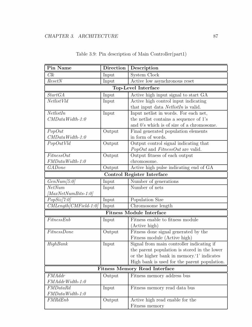
CHAPTER 3. ARCHITECTURE 87
Table 3.9: Pin description of Main Controller(part1)
Pin Name Direction Description
Clk Input System ClockResetN Input Active low asynchronous reset
Top-Level Interface
StartGA Input Active high input signal to start GANetlistVld Input Active high control input indicating
that input data NetlistIn is valid.NetlistIn Input Input netlist in words. For each net,CMDataWidth-1:0 the netlist contains a sequence of 1’s
and 0’s which is of size of a chromosome.PopOut Output Final generated population elementsCMDataWidth-1:0 in form of words.PopOutVld Output Output control signal indicating that
PopOut and FitnessOut are valid.FitnessOut Output Output fitness of each outputFMDataWidth-1:0 chromosome.GADone Output Active high pulse indicating end of GA
Control Register Interface
GenNum[5:0] Input Number of generationsNetNum Input Number of nets[MaxNetNumBits-1:0]PopSiz[7:0] Input Population SizeCMLength[CMField-1:0] Input Chromosome length
Fitness Module Interface
FitnessEnb Input Fitness enable to fitness module(Active high)
FitnessDone Output Fitness done signal generated by theFitness module (Active high)
HighBank Input Signal from main controller indicating ifthe parent population is stored in the loweror the higher bank in memory.‘1’ indicatesHigh bank is used for the parent population.
Fitness Memory Read Interface
FMAddr Output Fitness memory address busFMAddrWidth-1:0FMDataRd Input Fitness memory read data busFMDataWidth-1:0FMRdEnb Output Active high read enable for the
Fitness memory

CHAPTER 3. ARCHITECTURE 88
Table 3.10: Pin description of Main Controller(part2)
Pin Name Direction Description
Crossover and Mutation Module Interface
CrossoverEnb Input Crossover enable to crossover module(Active high)
CrossoverDone Input Crossover done signal generated by theCrossover and mutation module signifyingthe end of Crossover and mutation process.(Active high)
Child1Addr Output Starting address in chromosome memory[FMAddrWidth-2:0] where child1 has to be stored.Child2Addr Output Starting address in chromosome memory[FMAddrWidth-2:0] where child2 has to be stored
Selection Module Interface
SelectionEnb Output Selection enable to Selection module(Active high)
SelectionDone Input Selection done signal generated by theselection module signifying the end ofselection process for two parents.(Active high)
Chromosome Memory Read/Write Interface
CMAddrRd Output Chromosome memory read address busFMAddrWidth+CMField-1:0CMDataRd Input Chromosome memory read data busCMDataWidth-1:0CMRdEnb Output Active high read enable for the
Chromosome memoryCMAddrWd Output Chromosome memory write address busFMAddrWidth+CMField-1:0CMDataWr Output Chromosome memory write data busCMDataWidth-1:0CMWrEnb Output Active high write enable for the
Chromosome memory
Netlist Memory Write Interface
NMAddr Output Netlist memory address busFMAddrWidth+CMField-1:0NMDataWr Output Netlist memory write data busCMDataWidth-1:0NMWrEnb Output Active high write enable for the
Netlist memory

CHAPTER 3. ARCHITECTURE 89
Main Controller
CM
Dat
aRd
CM
RdE
nb
CM
Add
rRd
NM
Add
rRd
NM
RdE
nb
NM
Dat
aRd
FM
Add
rWr
FM
WrE
nb
FM
Dat
aWr
Fitness MemoryWrite Interface
ChromosomeMemory Read
Interface
Netlist MemoryRead Interface
Clk
ResetN
StartGA
Netlist Vld
Netlist In
PopOut
PopOutVld
FitnessOut
GADone
CM
Dat
aWr
CM
WrE
nb
CM
Add
rWr
Pop
Siz
Gen
Num
Net
Num
CM
Leng
th
HighBank
SelectionEnb
SelectionDone
CrossoverEnb
CrossoverDone
Child1Addr
Child2Addr
FitnessEnb
FitnessDone
To
p-l
evel
IO's
Control Registers
Fitn
essM
od
ule
Interface
Cro
ssover
Mo
du
leIn
terface
Selectio
nM
od
ule
Interface
Figure 3.22: Pin description of Main Controller Module
reaches the generation count loaded into GenNum control register. With each
generation, the generation count is incremented by one.
4. At the end of the last generation, the Main Controller enables the Fitness
module for one last time and outputs the final population and final fitness
using the top-level output signals.
The state diagram of the main controller state machine is shown in Figure 3.29
and the detailed description is shown in Figure 3.28.

CHAPTER 3. ARCHITECTURE 90
Clk
CPUWr
CPUAddr
CPUData
Register Write
Operation
Din
Figure 3.23: Control Register write Timings
Clk
NetlistVld
NetlistIn
StartGA
Figure 3.24: Control Input data and control Timings
Clk
GADone
StartGA
PopOutVld
PopOut
FitnessOut
Figure 3.25: Core output data and control timings

CHAPTER 3. ARCHITECTURE 91
Clk
WrEnb
AddrWr Addr AddrRd
Valid Data DataWr
RdEnb
DataRd Valid Data
Memory Write
Operation
Memory Read
Operation
Figure 3.26: Single port memory access timings
Clk
WrEnb
AddrWr AddrWr
Valid Data DataWr
RdEnb
DataRd Valid Data
Memory Write
Operation
Memory Read
Operation
AddrRd AddrRd
Figure 3.27: Dual port memory access timings

CHAPTER 3. ARCHITECTURE 92
CHROMOSOME COUNTER
POPULATION COUNTER
NETLIST COUNTER
GENERATION COUNTER
CHILD COUNTER
MAIN CONTROLLER STATE MACHINE
RANDOM NUMBER
GENERATOR
Top Level IO’s
Selection Module Interface
Crossover Module Interface
Fitness Module Interface
Control Register Interface
Fitness Memory Interface
Chromosome Memory Interface
Netlist Memory Interface
Figure 3.28: Detailed Description of Main Controller.

CHAPTER 3. ARCHITECTURE 93
stIdle
Reset
stload Netlist
stInitializePop
stFitness
stSelection
stCrossover
StartGA ='1'
AddrCntDone='1'PopCntDone='1'
FitnessDone='1'&&
GenCntDone = '0'
SelectionDone='1'
if (NetlistVld =1) AddrCntEnb ='1'; NMAddrWrInt = AddrCnt; NMWrEnbInt ='1'; NMDataWrInt = Netlist;
AddrCntRst ='1';LoadAddrCnt = '1';AddrCntMax=PSize*CLength;
AddrCntEnb ='1';GenerateRand ='1'CMAddrWrInt ='1';CMWrEnbInt ='1';CMDataWrInt=Rand(7:0);
RstHighBank ='1';Rst all CountersLoadAddrCnt ='1';AddrCntMax= NumOfNets*Clength;
FitnessEnb ='1';GenerationCntEnb ='1';
ChildCntRst ='1';
SelectionEnb ='1';
CrossoverEnb ='1';
stOutputResults
stPreIdle
CrossoverDone='1'&&
ChildCntDone='0'
CrossoverDone='1'&&
ChildCntDone='1'
ToggleHighBank ='1';ChildCntEnb ='1';GenCntEnb ='1';
ChildCntEnb ='1';
CMCntEnb='1'PopCntEnb='1'CMRdEnbInt='1'PopOutInt=CMDataRdFMRdEnbInt='1'FitnessOutInt= FMDataRdPopOutVldInt=CMRdEnbIntD2
FitnessDone='1'&&
GenCntDone = '1'
GADoneInt= '1'
AddrCntDone='1'
Figure 3.29: State Diagram of Main Controller Module
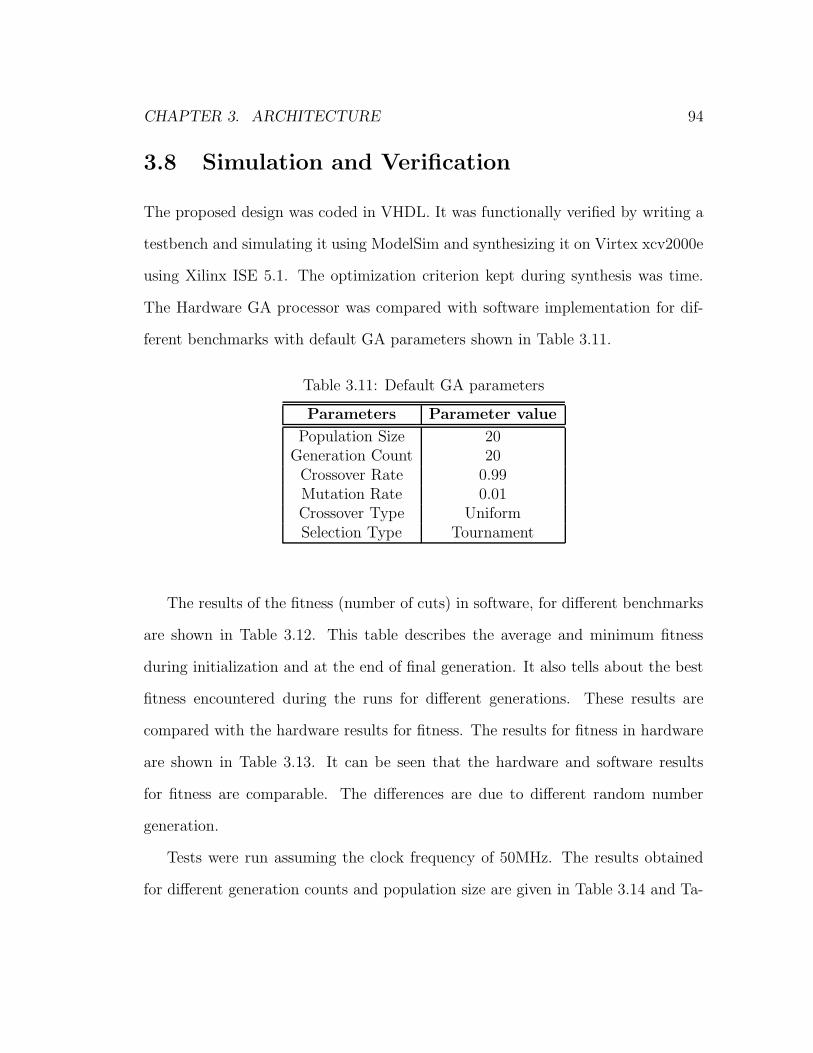
CHAPTER 3. ARCHITECTURE 94
3.8 Simulation and Verification
The proposed design was coded in VHDL. It was functionally verified by writing a
testbench and simulating it using ModelSim and synthesizing it on Virtex xcv2000e
using Xilinx ISE 5.1. The optimization criterion kept during synthesis was time.
The Hardware GA processor was compared with software implementation for dif-
ferent benchmarks with default GA parameters shown in Table 3.11.
Table 3.11: Default GA parameters
Parameters Parameter value
Population Size 20Generation Count 20Crossover Rate 0.99Mutation Rate 0.01Crossover Type UniformSelection Type Tournament
The results of the fitness (number of cuts) in software, for different benchmarks
are shown in Table 3.12. This table describes the average and minimum fitness
during initialization and at the end of final generation. It also tells about the best
fitness encountered during the runs for different generations. These results are
compared with the hardware results for fitness. The results for fitness in hardware
are shown in Table 3.13. It can be seen that the hardware and software results
for fitness are comparable. The differences are due to different random number
generation.
Tests were run assuming the clock frequency of 50MHz. The results obtained
for different generation counts and population size are given in Table 3.14 and Ta-

CHAPTER 3. ARCHITECTURE 95
Table 3.12: Software Fitness Results
Benchmarks Initial Initial Final Final BestAverage Minimum Average Minimum FitnessFitness Fitness Fitness Fitness
net9 mod10 6 3 1 1 1net12 mod15 7 4 1 1 1net15 mod10 11 8 4 4 4
Pcb1 20 16 9 9 9Chip3 123 107 17 12 10Chip4 130 119 46 37 35Chip2 152 136 46 39 39Chip1 184 172 38 27 20Prim1 564 538 109 93 87Prim2 1942 1897 255 200 188Bio 3388 3313 295 223 216
Table 3.13: Hardware Fitness Results
Benchmarks Initial Initial Final Final Best BestSoftware Software Software Software Software HardwareAverage Minimum Average Minimum Fitness FitnessFitness Fitness Fitness Fitness
net9 mod10 6.4 3.0 1.0 1.0 1.0 1.0net12 mod15 7.5 4.0 1.0 1.0 1.0 2.0net15 mod10 11.5 8.0 4.2 4.0 4.0 4.0
Pcb1 20.0 16.0 9.0 9.0 9.0 10.0Chip1 184 172 38 27 20 22Chip3 123 107 17 12 10 12

CHAPTER 3. ARCHITECTURE 96
Table 3.14: Performance results for Hardware GA and Software GA for differentGeneration Count
Benchmarks Generation Software Hardware e Time(ms)Count Time (ms) CMDataWidth CMDataWidth
(8bit) (16 bit)
net9 mod10 20 100 0.53 0.45Nnets=9 60 300 1.60 1.35
Nmods=10 100 600 2.60 2.26
net12 mod15 20 200 0.67 0.57Nnets=12 60 400 2.03 1.71Nmods=15 100 600 3.38 2.86
net15 mod10 20 200 0.82 0.69Nnets=15 60 400 2.46 2.07Nmods=10 100 800 4.10 3.46
Pcb1 20 200 1.86 1.63Nnets=32 60 600 5.58 4.91Nmods=24 100 900 9.30 7.20
Chip1 20 1700 73.56 40.50Nnets=294 60 4800 222.82 121.25Nmods=300 100 8100 373.63 202.32
Chip3 20 1200 38.41 23.23Nnets=239 60 3400 115.06 69.52Nmods=274 100 5900 190.55 116.23

CHAPTER 3. ARCHITECTURE 97
Table 3.15: Performance results for Hardware GA and Software GA for differentpopulation size
Benchmarks Population Software Hardware Time(ms)Size Time (ms) CMDataWidth CMDataWidth
(8bit) (16 bit)
net9 mod10 20 100 0.53 0.45Nnets=9 60 300 1.59 1.34
Nmods=10 100 600 2.58 2.24
net12 mod15 20 200 0.67 0.57Nnets=12 60 400 2.01 1.70Nmods=15 100 700 3.36 2.84
net15 mod10 20 200 0.82 0.69Nnets=15 60 500 2.44 2.06Nmods=10 100 800 4.08 3.44
Pcb1 20 200 1.86 1.63Nnets=32 60 700 5.58 4.82Nmods=24 100 1100 9.30 7.20
Chip1 20 1700 73.56 40.50Nnets=294 60 4900 218.24 122.25Nmods=300 100 8800 362.92 203.60
Chip3 20 1200 38.41 23.23Nnets=239 60 3800 114.32 69.36Nmods=274 100 5700 189.21 115.32

CHAPTER 3. ARCHITECTURE 98
ble 3.15, respectively. Smaller benchmarks (Table 3.13 are used because size of the
memory governs the size of benchmark data. In order to prove the concept and
verify the design, smaller benchmarks are used, thus removing the requirement of
using large FPGA. The remaining GA parameters were assigned the default values
given in Table 3.11. From the simulations results, it is clear that the hardware im-
plementation is much faster than the software version. The software results shown
in Table 3.14 and Table 3.15 were achieved using SUN ULTRA10 440 MHz proces-
sor system. As seen, the speed increases to approximately 50 times the software
implementation. This tremendous increase in speed for hardware implementation is
mainly attributed to the fact that, during fitness evaluation, if a cut is determined
for a net at any time, the remaining words for that net and the chromosome are
not read from the memory. This eliminates the time wasted by reading redundant
information from the Chromosome and Netlist memories. The hardware processing
speed can further be increased by increasing the Chromosome memory data bus
width because this enables more computations to be performed in parallel.
Table 3.16: Synthesis Report
Device Virtex xcv2000eSlices 334 out of 19200 (1.7%)CLB’s 167Equivalent Gate Count 6044Max Clock Frequency 123 MHz
Synthesis results are shown in Table 3.16. It is evident from Table 3.16 that
minimal hardware resources are utilized. Since the simulation results shown in
Table 3.14 and Table 3.15 are obtained by assuming a 50 MHz clock frequency,

CHAPTER 3. ARCHITECTURE 99
the improvement in speed can be increased to more than 100 times the software
implementation with a maximum tolerable clock frequency of 123 MHZ.
3.9 Summary
In this research, a GA Processor is designed which is used to solve circuit parti-
tioning problem. The architecture employs a combination of pipelining and par-
allelization to achieve speedups over software based GA. Results produced by the
proposed architecture are very encouraging. At a frequency of 123 MHz, 100 times
improvement in processing speed over software implementation is achieved. Min-
imal amount of hardware resources are utilized. The area/gate utilization of the
FPGA is small (Table 3.16), thus reduces the hardware resources needed. More-
over, the architecture proposed is implemented on a single FPGA. The design uses
the configurable parameters (generics), using which the hardware can be changed
based upon the size of the application the hardware is required to support. This
makes the architecture flexible. Since some of the modules in the design can be re-
used for other problems as well, the design is modular. The operational parameters
like population size, generation count etc. can be easily changed during run-time,
as the design has control registers with simple read/write interface. Therefore, it is
clear from the discussion that the proposed design was able to meet all the system
specifications and requirements.
After simulation and synthesis this architecture was mapped onto CMCs Rapid
Prototyping Platform(RPP) to verify its functionality on actual hardware. The
implementation and mapping of the design is explained in the next chapter.

Chapter 4
Implementation and Mapping
In the previous chapter a detailed architecture of a GA Processor was presented
and verified. This architecture can be mapped onto reconfigurable hardware plat-
form. This chapter describes the system operation of the Rapid Prototyping Plat-
form(RPP) and discuses the implementation details for the proposed architecture
on this platform. It is crucial to understand the architecture of the RPP, in order
to efficiently implement and map the GA processor. The detail functionality of
each block of RPP is explained in Appendix B. In order to implement and map the
GA Processor onto RPP, more modules were designed. The functionality of each
module is described in this chapter and the VHDL code for these modules is in [?].
4.1 Overview and System Operation of RPP
In this section, the CMC’s Rapid-Prototyping Platform (RPP) is explained which
was used to map the Genetic Algorithm Processor on actual hardware. CMC’s
100

CHAPTER 4. IMPLEMENTATION AND MAPPING 101
Rapid-Prototyping Platform (RPP) consists of hardware and software components
to enable the prototyping and design of complex, embedded systems based around
an ARM7TDMI microprocessor. The RPP features two daughtercards, both housed
on the same motherboard (ARM’s Integrator/AP board). The two daughtercards
are:
1. The ARM7TDMI microprocessor core(core module)
2. The ARM Integrator LM-XCV600E+ module which is a re-programmable
hardware module, featuring a Xilinx Virtex-2000E FPGA that enables designs
of up to 2 million FPGA gates(Logic module).
The ARM’s Integrator/AP board(motherboard) allows stacking multiple core
(e.g., ARM7, ARM9) and logic (Xilinx or Altera) modules, as well as the addition
of PCI cards for I/O. CMC provides and supports the RPP as a single ARM7TDMI
and Xilinx module system. Because the RPP provides a software-programmable
microprocessor as well as a hardware module, the design flow for the RPP involves
both software and hardware design flows and tools.
In addition, there is the ARM Multi-ICE unit which is used to communicate
between the host PC and either the logic module or core module as shown in Fig-
ure 4.1. Multi-ICE is the Embedded-ICE logic debug solution for ARM. It enables
to debug software running on ARM processor cores that include the Embedded-ICE
logic. It provides the software and hardware interface between a Joint Test Action
Group (JTAG) port on the hardware using a small interface unit and a Windows
or UNIX debugger using the ARM Debug Interface (RDI) running on the work-
station. It consists of an interface unit that connects the parallel port of the host

CHAPTER 4. IMPLEMENTATION AND MAPPING 102
Workstation
CORE MODULE
LOGIC MODULE
MULTI-ICE Connection
Integrator/AP Motherboard
Figure 4.1: Connection of Host to Rapid Prototyping Platform
PC to the JTAG interface of an ASIC that includes the debug and Embedded-ICE
capability. Also, a 128 MB SRAM DIMM is installed on the core module to expand
the available processor memory.
In brief, Multi-ICE is used to communicate between the host PC and either the
logic module or core module. It programs the ARM processor by downloading the
programs in C and also downloads the design to FPGA in logic module which is
written in VHDL code from the host PC. The communication between the core
module, the motherboard and logic module is through the standard AMBA buses
(AHB, APB and ASB). The different components are explained briefly in Appendix
B.
4.2 Implementation Details
In the previous chapter, the details of the architecture of GA processor were ex-
plained. In order to implement and map the GA Processor on RPP, additional

CHAPTER 4. IMPLEMENTATION AND MAPPING 103
modules are required for interfacing system bus with GA Processor. This section
describes the implementation details for the GA Processor.
4.2.1 System Description for Top level Implementation
The GA Processor is tested and implemented on CMC’s Rapid prototyping Plat-
form. The main blocks which are involved during implementation are shown in
Figure 4.2
1. The core module: The core module contains the ARM processor and a
memory controller FPGA. The host computer programs the ARM processor
using the Multi ICE. The ARM processor configures the memory controller
and tests the ZBT SRAM which is located on logic module. The core module
FPGA implements the system bus bridge. The system bus bridge provides
the AMBA interface between the memory bus on the core module and the
system bus on the motherboard. It allows the processor to access the interface
resources on other modules and the motherboard. The details of AMBA
specification is given in Appendix A. SDRAM is used for memory expansion
and it also provides support for Dual In Line Memory Modules(DIMMs).
2. The Logic module: The Logic Module contains Xilinx xcv2000E VirtexE
FPGA and 1MB ZBT SRAM. When the complete system for GA Processor
is synthesized for Xilinx VirtexE family and target device of xcv2000E , a .bit
file is generated. This file is implemented to logic module FPGA using Multi
ICE. In addition there is a 1MB ZBT SRAM, which stores the complete data
for the design(including netlist and GA parameters).

CHAPTER 4. IMPLEMENTATION AND MAPPING 104
SYSTEM CONTROLLER FPGA
ARM PROCESSOR
MEMORY CONTROLLER
FPGA
SD - RAM
ZBT SRAM
XILINX- xcv2000E FPGA
AMBA System Bus Communication
CORE MODULE LOGIC MODULE
Integrator/AP Motherboard
Figure 4.2: System Description for Top Level Implementation

CHAPTER 4. IMPLEMENTATION AND MAPPING 105
3. The Integrator/AP(motherboard): These two modules(core module and
logic module) are stacked on Integrator/AP. The motherboard contains sys-
tem controller FPGA that implements the system bus interface to core and
logic modules. It also provides clock generators that supplies clock for the
system bus.
4.2.2 Functional description of the Logic-module FPGA de-
sign
In order to test and implement the GA Processor as part of complete system, it
is implemented on VirtexE FPGA xcv2000E, along with GA Controller, AHB Top
Level Controller, and a multiplexer as shown in Figure 4.3. A description of the
modules inside the FPGA is explained below:
1. AHB Top Level Controller: This block receives the input from the ARM
processor via AMBA system bus. The netlist and GA parameters are loaded
into ZBT SRAM. ARM processor writes to the control register which en-
ables the bit called EnbGACtl in this register to start the GA process. After
enabling theEnbGACtl bit, ARM keeps on polling the value of this bit via
AMBA. If this bit is ‘0’, the ARM processor starts reading the output data
(population and fitness) from the ZBT SRAM. This data is then displayed
on the standard output-monitor of the host, where it can be verified. The
connection between the host and Rapid Prototyping Platform is with Multi
ICE.
The AHB Top Level controller contains all high speed peripherals, decoder

CHAPTER 4. IMPLEMENTATION AND MAPPING 106
GA PROCESSOR GA
CONTROLLER
AMBA TOP LEVEL
CONTROLLER
MULTIPLEXER
ZBT SRAM
CM FM NM
FPGA
Input From
System Bus
AMBA
Figure 4.3: System Description of the Logic-module FPGA

CHAPTER 4. IMPLEMENTATION AND MAPPING 107
and all necessary support and glue logic to make a working system as shown
in Figure 4.4.
ADDRESS DECODER
AHB TO APB BRIDGE
AHB SSRAM CONTROLLER
REGISTER PERIPHERAL
INTERRUPT CONTROLLER
AHB SYSTEM
BUS
Figure 4.4: AHB Top Level Controller
2. GA Controller: This block communicates between GA Processor, ZBT
SRAM and AHB Top Level Controller. When the ARM processor enables the
bit EnbGACtl of the control register through the AHB Top Level Controller,
GA controller starts loading the GA parameters and netlist from ZBT SRAM
to GA processor after generating theStartGA signal for GA Processor and
executes all its operations. Finally, it sends the output data to GA Controller,
which further sends the data to ZBT SRAM for storage. After data has been
stored completely in ZBT RAM, GACtlReset signal is sent to AHB Top Level
controller. This signal disables the EnbGACtl signal and the output is sent
to the host computer.
3. Multiplexer: It multiplexes the control and data signals generated by GA

CHAPTER 4. IMPLEMENTATION AND MAPPING 108
Controller and AHB Top Level Controller for ZBT RAM. It also multiplexes
the data and control signals of ZBT SRAM generated for these two blocks.
Select is done based upon the EnbGACtl signal which indicates that GA
Controller is active.
Figure 4.5 shows the system level flow diagram for implementation on RPP.

CHAPTER 4. IMPLEMENTATION AND MAPPING 109
Load Netlist and Control Register values into ZBTRAM
Write ‘1' into ‘EnableGACtl’ bit of GA Controller Register
Read Enable GA Controller Register
Read Final Population from ZBTRAM
START
END
Check ‘EnableGACtl’ bit of GA Controller Register
Read Control Register values from ZBTRAM and load GA Processor
registers
Generate ‘StartGA’ pulse to start GA Processor
Load Netlist data into GA Processor from ZBTRAM
Read Final Population from GA Processor and write into ZBTRAM
Reset ‘EnableGACtl’ bit in Control Register
SOFTWARE
YES
NO
NO
YES
Is ‘EnableGACtl’ bit =’1' ?
Is ‘EnableGACtl’ bit =’1' ?
HARDWARE
Figure 4.5: System level Implementation Flow Diagram

CHAPTER 4. IMPLEMENTATION AND MAPPING 110
4.2.3 Address Mapping
The memory map for the logic module is shown in the Figure 4.6. This shows the
locations to which the logic module are assigned by the main address decoder on
motherboard. The diagram also shows how the whole design decodes the address
space for logic module.
LOGIC MODULE 0
LOGIC MODULE 1
LOGIC MODULE 2
LOGIC MODULE 3
CORE MODULE ALIAS MEMORY
PCI
CORE MODULE / MOTHERBOARD MEMORY
AND PERIPHERALS
BUS ERROR RESPONSE
SSRAM
INTERRUPT CONTROLLER
LM REGISTERS
0XF0000000
0XE0000000
0XD0000000
0XC0000000
0XC0000000
0XC1000000
0XC2000000
0XC20FFFF
0XCFFFFFF
Figure 4.6: Address Mapping In Logic Module
4.3 Results and Conclusions
The complete system was tested and verified on the RPP for different benchmarks
data. Tests were performed for different generation counts and average and best

CHAPTER 4. IMPLEMENTATION AND MAPPING 111
fitness results were obtained. The implementation results obtained on the RPP were
verified for best fitness, average fitness, and solution feasibility by writing a result-
checker program in C. Table 4.1 shows the test results for different benchmarks
with population size of 16 and different generation counts.
Table 4.1: RPP test results with different generation counts for different Bench-marks
Benchmarks Generation Count Average Fitness Best Fitness
Pcb1 2 16.8 14.0Nnets=32 4 18.5 14.0Nmods=24 6 15.0 11.0
8 13.7 11.010 12.0 10.012 10.4 10.014 10.0 10.0
net9-mod10 2 4.8 1.0Nnets=9 4 3.7 1.0
Nmods=10 6 1.6 1.08 1.0 1.010 1.0 1.0
net12-mod15 2 6.7 3.0Nnets=12 4 5.3 3.0Nmods=15 6 4.2 2.0
8 2.5 2.010 2.0 2.012 2.0 2.0
net15-mod10 2 9.4 6.0Nnets=15 4 7.9 6.0Nmods=10 6 6.7 4.0
8 5.8 4.010 4.4 4.012 4.0 4.014 4.0 4.0
The plots for average and best fitness results for the different benchmarks are

CHAPTER 4. IMPLEMENTATION AND MAPPING 112
shown in Figure 4.7.
2 4 6 8 10 12 148
10
12
14
16
18
20
22
Fitn
ess
Generation Count
pcb1 Results
Average FitnessBest Fitness
2 4 6 8 100
1
2
3
4
5
6
Fitn
ess
Generation Count
net9_mod10 Results
Average FitnessBest Fitness
2 4 6 8 10 120
2
4
6
8
Fitn
ess
Generation Count
net12_mod15 Results
Average FitnessBest Fitness
2 4 6 8 10 12 143
4
5
6
7
8
9
10
11F
itnes
s
Generation Count
net15_mod10 Results
Average FitnessBest Fitness
Figure 4.7: Fitness plots for different benchmarks.
4.4 Summary
In this chapter, GA processor is implemented and mapped onto RPP. Since block-
RAMs internal to the FPGA are used as chromosome, netlist, and fitness memories,
there is a restriction on the size of problems that can be solved by the RPP im-
CHAPTER 4. IMPLEMENTATION AND MAPPING 113
plementation. However, just to prove the concept and to verify that the design is
implemented correctly in hardware, the sizes of the block-RAMs used are sufficient.
A more practical way of implementing would be to use memories external to the
FPGA, as in this case there would not be a strict restriction on the size of problem
that can be solved by the implemented design. However, such an implementation
would require a more complex memory-interface timing constraints and maybe a
dedicated circuit-board designed specifically for the GA hardware.
One of the major challanges in hardware implementation is that the observabil-
ity of the internal signals in the design is greatly reduced. In order to facilitate
debugging of the design, internal states of the state-machines were made observ-
able to the ARM processor through the AMBA interface. These debug signals
were implemented in the form of a control register in the peripheral address space
of the APB. Having such debug signals greatly helped the debugging stage of the
implementation.

Chapter 5
Conclusions and Future Directions
In view of the increasing complexity of VLSI circuits[?], there is a growing need for
sophisticated CAD tools to automate the synthesis, analysis, and verification steps
in the design of VLSI systems.
In this research a new architecture for implementing the genetic algorithm in
hardware is proposed. Although the architecture is designed specifically to solve
the circuit-partitioning problem, some of the modules in the design can be re-used
for other problems as well which makes the design to be modular. These include the
Selection Module, Crossover Module, the LFSR based random number generator,
and most of the Main Controller. The design takes into account the practical
limitations of memory data bus imposed by the memory chips available. In order
to enable the use of almost any memory chip along with the design, the design uses
configurable parameters (generics) which can easily change the memory address
and data bus widths during compilation time.
The functional correctness of the design was verified by using Modelsim simula-
114

CHAPTER 5. CONCLUSIONS AND FUTURE DIRECTIONS 115
tor. The simulation was used to analyze its performance and identify its bottleneck.
The design was synthesized for a maximum clock frequency of 123 MHz on Virtex
xcv2000e. At this frequency the design achieves more than 100 times improvement
in processing speed over the software implementation. These improvements were
due to pipelined architectures. It is also evident from the synthesis results that min-
imal hardware resources are utilized. The architecture proposed in this research is
implemented on a single FPGA, thus reducing the hardware resources needed.
Therefore, due to reprogrammability of FPGAs, the proposed architecture pos-
sessed the speed of hardware while retaining the flexibility of a software implemen-
tation. This GA processor can be useful in many applications where software-based
GA implementations are too slow.
5.1 Future Work
There are many ways to extend the proposed design by simple modifications in the
internal architecture and the platform implementation.
5.1.1 Architecture Enhancements
This design was used to solve two-way circuit partitioning problem with tourna-
ment selection and uniform crossover. Other Genetic Algorithm operators could be
implemented like, multi-point cross-over, partially mapped crossover and different
selection methods as well. The design can be extended to solve multi-way circuit
partitioning problem. The design can also be enhanced by incorporating a local
search engine to create a hybrid memetic GA. The chromosome representation used

CHAPTER 5. CONCLUSIONS AND FUTURE DIRECTIONS 116
in this project requires a relatively large amount of external memory to store the
population and netlist. Alternate chromosome representations can be explored in
order to reduce the memory requirements.
5.1.2 Platform-mapping Enhancements
Hardware/software co-design can be implemented in which the reconfigurable pro-
cessors will integrate processor cores and reconfigurable units, much closer than
today’s devices do. The results of such an implementation can be compared with
those of the current implementation.
In the present implementation, the different memories used by the GA processor
are implemented using FPGA’s block-RAMs. This limits the size of the problem
that can be solved using this hardware. In order to design a more generic hardware
which can solve large-sized problems, these memories can be implemented external
to the FPGA using on-board memory chips.

Appendix A
Introduction to AMBA Buses
A.1 Overview of the AMBA specification
The Advanced Microcontroller Bus Architecture (AMBA) specification defines an
on chip communications standard for designing high-performance embedded micro-
controllers.
Three distinct buses are defined within the AMBA specification:
1. The Advanced High-performance Bus (AHB).
2. The Advanced System Bus (ASB).
3. The Advanced Peripheral Bus (APB).
A test methodology is included with the AMBA specification which provides an
infrastructure for modular macrocell test and diagnostic access.
1. Advanced High-performance Bus (AHB):
117

APPENDIX A. INTRODUCTION TO AMBA BUSES 118
The AMBA AHB is for high-performance, high clock frequency system mod-
ules. The AHB acts as the high-performance system backbone bus. AHB
supports the efficient connection of processors, on-chip memories and off-chip
external memory interfaces with low-power peripheral macrocell functions.
AHB is also specified to ensure ease of use in an efficient design flow using
synthesis and automated test techniques.
2. Advanced System Bus (ASB):
The AMBA ASB is for high-performance system modules. AMBA ASB is
an alternative system bus suitable for use where the high-performance fea-
tures of AHB are not required. ASB also supports the efficient connection
of processors, on-chip memories and off-chip external memory interfaces with
low-power peripheral macrocell functions.
3. Advanced Peripheral Bus (APB):
The AMBA APB is for low-power peripherals. AMBA APB is optimized
for minimal power consumption and reduced interface complexity to support
peripheral functions. APB can be used in conjunction with either version of
the system bus.
A.2 A typical AMBA-based microcontroller
An AMBA-based microcontroller typically consists of a high-performance system
backbone bus (AMBA AHB or AMBA ASB), able to sustain the external memory
bandwidth, on which the CPU, on-chip memory and other Direct Memory Ac-
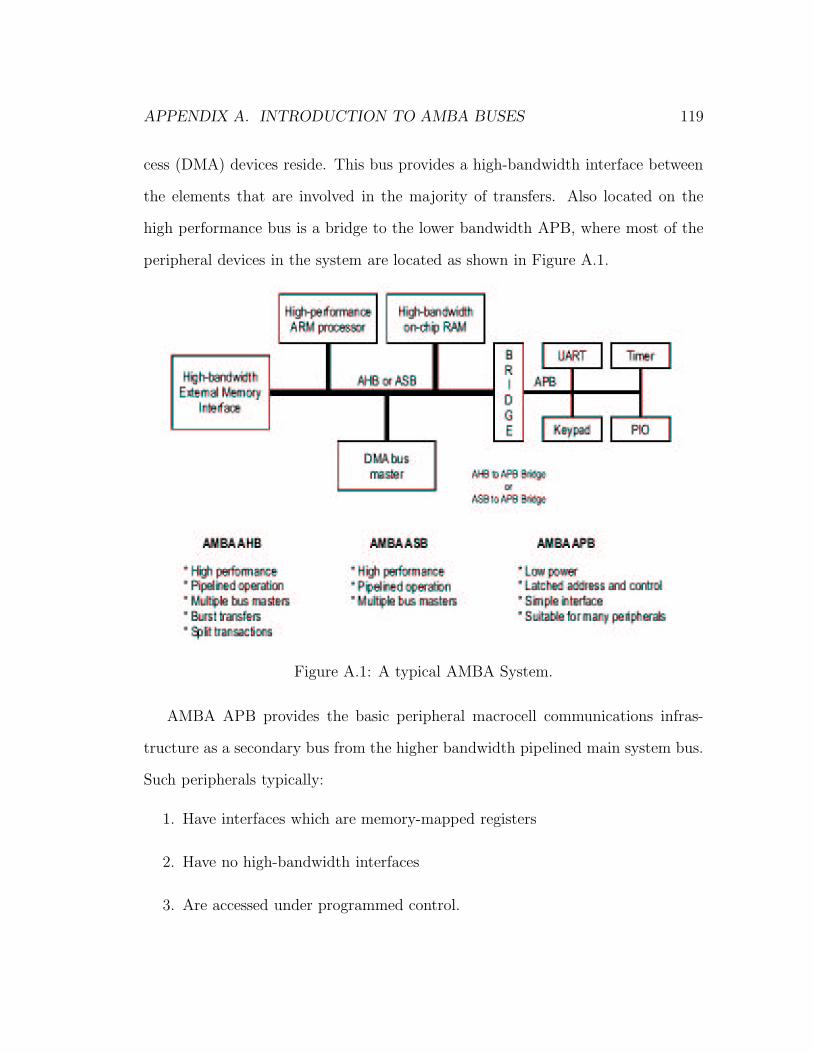
APPENDIX A. INTRODUCTION TO AMBA BUSES 119
cess (DMA) devices reside. This bus provides a high-bandwidth interface between
the elements that are involved in the majority of transfers. Also located on the
high performance bus is a bridge to the lower bandwidth APB, where most of the
peripheral devices in the system are located as shown in Figure A.1.
Figure A.1: A typical AMBA System.
AMBA APB provides the basic peripheral macrocell communications infras-
tructure as a secondary bus from the higher bandwidth pipelined main system bus.
Such peripherals typically:
1. Have interfaces which are memory-mapped registers
2. Have no high-bandwidth interfaces
3. Are accessed under programmed control.

APPENDIX A. INTRODUCTION TO AMBA BUSES 120
The external memory interface is application-specific and may only have a narrow
data path, but may also support a test access mode which allows the internal AMBA
AHB, ASB and APB modules to be tested in isolation with system-independent
test sets.
A.3 Terminology
The following terms are used throughout this specification.
1. Bus cycle: A bus cycle is a basic unit of one bus clock period and for the
purpose of AMBA AHB or APB protocol descriptions is defined from rising-
edge to rising-edge transitions. An ASB bus cycle is defined from falling-edge
to falling-edge transitions. Bus signal timing is referenced to the bus cycle
clock.
2. Bus transfer: An AMBA ASB or AHB bus transfer is a read or write
operation of a data object, which may take one or more bus cycles. The bus
transfer is terminated by a completion response from the addressed slave. The
transfer sizes supported by AMBA ASB include byte (8-bit), halfword (16-bit)
and word (32-bit). AMBA AHB additionally supports wider data transfers,
including 64-bit and 128-bit transfers. An AMBA APB bus transfer is a read
or write operation of a data object, which always requires two bus cycles.
3. Burst operation: A burst operation is defined as one or more data transac-
tions, initiated by a bus master, which have a consistent width of transaction
to an incremental region of address space. The increment step per transac-

APPENDIX A. INTRODUCTION TO AMBA BUSES 121
tion is determined by the width of transfer (byte, halfword, word). No burst
operation is supported on the APB.
A.4 Introducing the AMBA AHB
AHB is a new generation of AMBA bus which is intended to address the require-
ments of high-performance synthesizable designs. It is a high-performance system
bus that supports multiple bus masters and provides high-bandwidth operation.
AMBA AHB implements the features required for high-performance, high clock
frequency systems including:
1. Burst transfers
2. Split transactions
3. Single-cycle bus master handover
4. Single-clock edge operation
5. Non-tristate implementation
6. Wider data bus configurations (64/128 bits).
Bridging between this higher level of bus and the current ASB/APB can be done
efficiently to ensure that any existing designs can be easily integrated. An AMBA
AHB design may contain one or more bus masters, typically a system would contain
at least the processor and test interface. However, it would also be common for a
Direct Memory Access (DMA) or Digital Signal Processor (DSP) to be included as

APPENDIX A. INTRODUCTION TO AMBA BUSES 122
bus masters. The external memory interface, APB bridge and any internal memory
are the most common AHB slaves. Any other peripheral in the system could also be
included as an AHB slave. However, low-bandwidth peripherals typically reside on
the APB. A typical AMBA AHB system design contains the following components:
1. AHB Master: A bus master is able to initiate read and write operations by
providing an address and control information. Only one bus master is allowed
to actively use the bus at any one time.
2. AHB slave: A bus slave responds to a read or write operation within a given
address-space range. The bus slave signals back to the active master the
success, failure or waiting of the data transfer.
3. AHB arbiter: The bus arbiter ensures that only one bus master at a time
is allowed to initiate data transfers. Even though the arbitration protocol is
fixed, any arbitration algorithm, such as highest priority or fair access can
be implemented depending on the application requirements. An AHB would
include only one arbiter, although this would be trivial in single bus master
systems.
4. AHB decoder: The AHB decoder is used to decode the address of each transfer
and provide a select signal for the slave that is involved in the transfer. A
single centralized decoder is required in all AHB implementations.

APPENDIX A. INTRODUCTION TO AMBA BUSES 123
A.4.1 Overview of AMBA AHB operation
Before an AMBA AHB transfer can commence the bus master must be granted
access to the bus. This process is started by the master asserting a request signal
to the arbiter. Then the arbiter indicates when the master will be granted use of the
bus. A granted bus master starts an AMBA AHB transfer by driving the address
and control signals. These signals provide information on the address, direction
and width of the transfer, as well as an indication if the transfer forms part of a
burst. Two different forms of burst transfers are allowed:
1. Incrementing bursts, which do not wrap at address boundaries.
2. Wrapping bursts, which wrap at particular address boundaries. A write data
bus is used to move data from the master to a slave, while a read data bus is
used to move data from a slave to the master.
Every transfer consists of:
1. An address and control cycle
2. One or more cycles for the data.
The address cannot be extended and therefore all slaves must sample the address
during this time. The data, however, can be extended using the HREADY signal.
When LOW this signal causes wait states to be inserted into the transfer and allows
extra time for the slave to provide or sample data.
During a transfer the slave shows the status using the response signals, HRESP[1:0]:

APPENDIX A. INTRODUCTION TO AMBA BUSES 124
1. OKAY: The OKAY response is used to indicate that the transfer is progress-
ing normally and when HREADY goes HIGH this shows the transfer has
completed successfully.
2. ERROR: The ERROR response indicates that a transfer error has occurred
and the transfer has been unsuccessful.
3. RETRY and SPLIT: Both the RETRY and SPLIT transfer responses indicate
that the transfer cannot complete immediately, but the bus master should
continue to attempt the transfer.
In normal operation a master is allowed to complete all the transfers in a particular
burst before the arbiter grants another master access to the bus. However, in order
to avoid excessive arbitration latencies it is possible for the arbiter to break up a
burst and in such cases the master must re-arbitrate for the bus in order to complete
the remaining transfers in the burst.
A.4.2 Basic Transfer
An AHB transfer consists of two distinct sections:
1. The address phase, which lasts only a single cycle.
2. The data phase, which may require several cycles. This is achieved using the
HREADY signal.
Figure A.2 shows the simplest transfer, one with no wait states.

APPENDIX A. INTRODUCTION TO AMBA BUSES 125
Figure A.2: Basic Transfer

APPENDIX A. INTRODUCTION TO AMBA BUSES 126
A.4.3 Address Decoding
A central address decoder is used to provide a select signal, HSELx, for each slave
on the bus. The select signal is a combinatorial decode of the high-order address
signals, and simple address decoding schemes are encouraged to avoid complex
decode logic and to ensure high-speed operation. A slave must only sample the
address and control signals and HSELx when HREADY is HIGH, indicating that
the current transfer is completing. Under certain circumstances it is possible that
HSELx will be asserted when HREADY is LOW, but the selected slave will have
changed by the time the current transfer completes. The minimum address space
that can be allocated to a single slave is 1kB. All bus masters are designed such that
they will not perform incrementing transfers over a 1kB boundary, thus ensuring
that a burst never crosses an address decode boundary. In the case where a system
design does not contain a completely filled memory map an additional default
slave should be implemented to provide a response when any of the nonexistent
address locations are accessed. If a NONSEQUENTIAL or SEQUENTIAL transfer
is attempted to a nonexistent address location then the default slave should provide
an ERROR response. IDLE or BUSY transfers to nonexistent locations should
result in a zero wait state OKAY response. Typically the default slave functionality
will be implemented as part of the central address decoder. Figure A.3 shows a
typical address decoding system and the slave select signals.

APPENDIX A. INTRODUCTION TO AMBA BUSES 127
Figure A.3: Address Decoding System.
A.4.4 AHB Bus Slave
An AHB bus slave responds to transfers initiated by bus masters within the system.
The slave uses a HSELx select signal from the decoder to determine when it should
respond to a bus transfer. All other signals required for the transfer, such as the
address and control information, will be generated by the bus master and are shown
in Figure A.4.
A.4.5 AMBA AHB signal list
This section contains an overview of the AMBA AHB signals (see Table A.1 and
Table A.2). All signals are prefixed with the letter H, ensuring that the AHB signals
are differentiated from other similarly named signals in a system design.
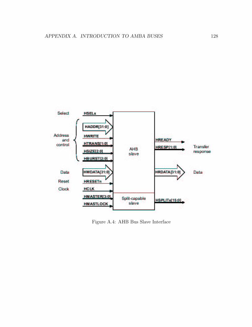
APPENDIX A. INTRODUCTION TO AMBA BUSES 128
Figure A.4: AHB Bus Slave Interface

APPENDIX A. INTRODUCTION TO AMBA BUSES 129
Table A.1: AMBA AHB signals(part1)
Name Source Description
HCLK Clock source This clock times all bus transfers. All signaltimings are related to the rising edge of HCLK.
HRESETn Reset controller The bus reset signal is active LOW and isused to reset the system and the bus.This isthe only active LOW signal.
HADDR[31:0] Master The 32-bit system address bus.HTRANS[1:0] Master Indicates the type of the current transfer,which
can be NONSEQUENTIAL, SEQUENTIAL, IDLEor BUSY.
HWRITE Master When HIGH this signal indicates a write transferand when LOW a read transfer.
HSIZE[2:0] Master Indicates the size of the transfer, which istypically byte (8-bit), halfword (16-bit) orword (32-bit). The protocol allows for largertransfer sizes up to a maximum of 1024 bits.
HBURST[2:0] Master Indicates if the transfer forms part of aburst. Four, eight and sixteen beat bursts aresupported and the burst may be eitherincrementing or wrapping.
HPROT[3:0] Master The protection control signals provideadditional information about a bus accessand are primarily intended for use by anymodule that wishes to implement some levelof protection. The signals indicate ifthe transfer is an opcode fetch or dataaccess, as well as if the transfer is aprivileged mode access or user mode access.For bus masters with a memory managementunit these signals also indicate whetherthe current access is cacheable or bufferable.

APPENDIX A. INTRODUCTION TO AMBA BUSES 130
Table A.2: AMBA AHB signals(part2)
Name Source Description
HWDATA[31:0] Master The write data bus is used to transferdata from the master to the bus slavesduring write operations. A minimum databus width of 32 bits is recommended.However, this may easily be extendedto allow for higher bandwidth operation.
HSELx Decoder Each AHB slave has its own slave selectsignal and this signal indicates thatthe current transfer is intended for theselected slave. This signal is simplya combinatorial decode of the address bus.
HRDATA[31:0] Slave The read data bus is used to transferdata from bus slaves to the bus masterduring read operations. A minimum databus width of 32 bits is recommended.However, this may easily be extendedto allow for higher bandwidth operation.
HREADY Slave When HIGH the HREADY signal indicates thata transfer has finished on the bus.This signal may be driven LOW toextend a transfer.
HRESP[1:0] Slave The transfer response provides additionalinformation on the status of a transfer.Four different responses are provided,OKAY,ERROR, RETRY and SPLIT.

Appendix B
Overview of Rapid Prototyping
Platform
B.1 Overview of the Integrator/AP
The Integrator/AP is the motherboard and supports up to four processors on plug-
in modules and provides clocks, bus arbitration and interrupt handling for them.
It also provides operating system support with flash memory, boot ROM and input
and output resources. The major features on the Integrator/AP (motherboard) are
as follows and the architecture is shown in Figure B.1
The system controller FPGA provides system control and interface as shown in
Figure B.2.
1. System controller FPGA that implements:
• System bus interface to core and logic module from the motherboard.
131

APPENDIX B. OVERVIEW OF RAPID PROTOTYPING PLATFORM 132
Figure B.1: ARM Integrator/AP Block Diagram

APPENDIX B. OVERVIEW OF RAPID PROTOTYPING PLATFORM 133
Figure B.2: Functional Block Diagram of System Controller FPGA on ARM Inte-grator/AP
• System bus arbiter provides bus arbitration for a total of six bus
masters, five of which can be core and logic modules.
• Interrupt controller handles interrupts which originate from periph-
eral controllers, from PCI bus, and from devices on any attached logic
modules.
• Peripheral input and output controllers
• Three counter/timers
• Reset controller initializes the Integrator/AP when the system is reset.
• System status and control registers allows software configuration
and control of the operation of Integrator/AP.

APPENDIX B. OVERVIEW OF RAPID PROTOTYPING PLATFORM 134
2. Clock generator that supply clocks for system bus, UARTs etc.
3. 32MB flash memory
4. 256KB boot ROM
5. 512KB SSRAM
6. Two serial ports (RS232DTE)
7. System expansion, supporting core and logic modules
8. PCI bus interface, supporting expansion on board
9. External bus interface (EBI), supporting memory expansion
In the system bus as shown in Figure B.3, there are three main system buses
(A [31:0], C [31:0], D [31:0]) routed between system controller FPGA on the ARM
Integrator/AP and FPGA’s on core and logic modules. In addition there is a fourth
bus B [31:0] routed between connectors.

APPENDIX B. OVERVIEW OF RAPID PROTOTYPING PLATFORM 135
Figure B.3: System Bus Architecture For Rapid Prototyping Platform
B.2 Overview of Core Module
The major components on the core module are as follows and the block diagram is
shown in figure B.4
1. ARM7TDMI microprocessor core
2. Core module FPGA that implements:
• SDRAM controller
• System bus bridge
• Reset controller
• Interrupt controller

APPENDIX B. OVERVIEW OF RAPID PROTOTYPING PLATFORM 136
Figure B.4: Block Diagram For Core Module
• Status, configuration and interrupt registers
3. Volatile memory comprising:
• Up to 256MB of SDRAM (optional)
• 256KB SSRAM
4. SSRAM controller
5. Clock generator
6. System bus connectors to motherboard and other modules
7. Multi-ICE, logic analyzer and optional trace connectors.
The core module FPGA contains five main functional blocks as shown in Fig-
ure B.5:

APPENDIX B. OVERVIEW OF RAPID PROTOTYPING PLATFORM 137
Figure B.5: FPGA functional Diagram for Core Module
1. SDRAM controller: The core module provides support for a single 16,32,64,128
or 256 MB SDRAM DIMM(Dual In Line Memory Modules).
2. Reset controller: This enables the core module to be reset as a standalone
unit or as part of an Integrator development system.
3. System bus bridge: It provides an asynchronous bus interface between the
local memory bus and system bus connecting the motherboard and other
modules.
4. Core module registers: These are status, configuration and interrupt registers.
5. Debug communication interrupts: The ARM7TDMI processor core incorpo-
rates EmbeddedICE hardware and provides a debug communications data
register that is used to pass data between the processor and JTAG equip-
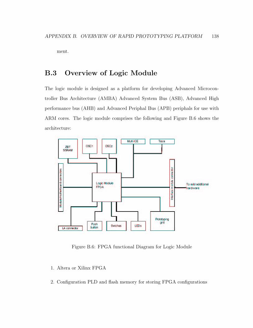
APPENDIX B. OVERVIEW OF RAPID PROTOTYPING PLATFORM 138
ment.
B.3 Overview of Logic Module
The logic module is designed as a platform for developing Advanced Microcon-
troller Bus Architecture (AMBA) Advanced System Bus (ASB), Advanced High
performance bus (AHB) and Advanced Periphal Bus (APB) periphals for use with
ARM cores. The logic module comprises the following and Figure B.6 shows the
architecture:
Figure B.6: FPGA functional Diagram for Logic Module
1. Altera or Xilinx FPGA
2. Configuration PLD and flash memory for storing FPGA configurations

APPENDIX B. OVERVIEW OF RAPID PROTOTYPING PLATFORM 139
3. 1MB ZBT SSRAM
4. Clock generators and reset sources
5. JTAG, trace and logic analyzers connectors
6. System bus connectors to motherboard and other modules which is imple-
mented according to AHB or APB specifications.
B.4 Rapid Prototyping Platform Design Flow
1. Design Specifications: The design flow starts with a set of design re-
quirments and system specifications, detailing the function of the system, as
well as the constraints such as clock speed, power, and operating conditions.
2. Algorithmic Design and Analysis: In the next step, the specifications
are translated into a high-level, algorithmic description of the system. This
algorithmic design and analysis step is usually implemented in C/C++. The
algorithmic description helps to fully understand the function of the system,
before architectural details are developed.
3. System Architecture Design: After optimizing the algorithm at high level,
the implementation process begins, where functional units are mapped to
various architectural units. This design process requires tools like Cadence’s
virtual Component Co-design(VCC). In a parallel activity, system architec-
ture is modeled with appropriate estimates on timing, power etc.In brief,
hardware/software partitioning partitioning is done at this stage.
APPENDIX B. OVERVIEW OF RAPID PROTOTYPING PLATFORM 140
4. Hardware:
• HDL Coding: The hardware design flow uses a hardware description
language (HDL), VHDL or Verilog, to create that portion of system
design. The complete hardware sub-system is specified as individual
blocks, interconnected by wires/buses. Design blocks can be regular
RTL code, state diagrams, flow charts, truth tables, or hierarchical block
diagrams.
• Functional Simulation: Once HDL is coded, it is verified through
functional simulation(using a simulator such as Synopsys VSS or Ca-
dence NC-Sim or Mentor Graphics Modelsim). The Testbench is cre-
ated alongside the HDL. This simulation is technology-independent, and
contains no timing or power data. The HDL code is modified and re-
simulated until the function is verified.
• Synthesis: After, functional simulation synthesis maps the RTL code
to logic gates. Tools like FPGA Compiler II from Synopsys perform
this task, using the constraints on timing etc., to optimize the design.
Using gate-level delays, designers can perform back-annotated timing
simulation. Re-using the functional testbench, this step confirms that
synthesis has not altered the design’s functionality. This simulation also
contains accurate timing information, therefore it can be determined if
actual design will operate within the constraints.
• Place and Route: After synthesis placement and routing is done using
Xilinx Design tools. This step maps the logic gates from synthesis to
APPENDIX B. OVERVIEW OF RAPID PROTOTYPING PLATFORM 141
functional units on the FPGA. The output of this step is a bitstream
file, which is a complete map of the design, configured for a particular
Xilinx part (e.g., Virtex 2000E-PQ540-6). This file can be downloaded
to the corresponding Xilinx part for the operation.
5. Software: Occuring parallel to the hardware design flow, the software de-
velopment design flow creates the code that runs on the microprocessor in
the system ( in the RPP case, this is an ARM7TDMI microprocessor). Soft-
ware development can involve several tools, including a real-time operating
system (RTOS), instruction-set simulator (ISS), and code development tools
(C/C++ compiler, linker, and assembler).

Appendix C
VHDL Code
C.1 GaTop.vhdlibrary ieee;library work;use ieee.std_logic_1164.all;use ieee.std_logic_unsigned.all;use work.components.all;
entity GaTop isgeneric(-- Fitness memory address/data widthFMAddrWidth : integer := 9;FMDataWidth : integer := 8;-- Chromosome memory data widthCMDataWidth : integer := 8;-- Width of chromosome field in CMAddr busCMField : integer := 3;-- Maximum bits used for number of netsMaxNetNumBits : integer := 8
);port(ResetN : in std_logic;Clk : in std_logic;-- CPU InterfaceCPUWr : in std_logic;CPUAddr : in std_logic_vector(3 downto 0);CPUData : in std_logic_vector(7 downto 0);-- Data and Control IO’sStartGA : in std_logic;
142

APPENDIX C. VHDL CODE 143
NetlistVld : in std_logic;NetlistIn : in std_logic_vector(CMDataWidth-1 downto 0);PopOut : out std_logic_vector(CMDataWidth-1 downto 0);PopOutVld : out std_logic;FitnessOut : out std_logic_vector(FMDataWidth-1 downto 0);GADone : out std_logic;-- Netlist Memory access signalsNMAddr : out std_logic_vector(MaxNetNumBits+CMField-1 downto 0);NMDataWr : out std_logic_vector(CMDataWidth-1 downto 0);NMWrEnb : out std_logic;NMDataRd : in std_logic_vector(CMDataWidth-1 downto 0);NMRdEnb : out std_logic;-- Chromosome Memory access signalsCMAddrRd : out std_logic_vector(FMAddrWidth+CMField-1 downto 0);CMDataRd : in std_logic_vector(CMDataWidth-1 downto 0);CMRdEnb : out std_logic;CMAddrWr : out std_logic_vector(FMAddrWidth+CMField-1 downto 0);CMDataWr : out std_logic_vector(CMDataWidth-1 downto 0);CMWrEnb : out std_logic;-- Fitness Memory access signalsFMAddr : out std_logic_vector(FMAddrWidth-1 downto 0);FMDataRd : in std_logic_vector(FMDataWidth-1 downto 0);FMRdEnb : out std_logic;FMDataWr : out std_logic_vector(FMDataWidth-1 downto 0);FMWrEnb : out std_logic
);end entity GaTop;
architecture rtl of GaTop is
-- Selection Module signalssignal SelectionEnb : std_logic;signal HighBank : std_logic;signal SelectionDone : std_logic;signal Parent1Addr : std_logic_vector(FMAddrWidth-2 downto 0);signal Parent2Addr : std_logic_vector(FMAddrWidth-2 downto 0);
-- Crossover Module signalssignal CrossoverEnb : std_logic;signal CrossoverDone : std_logic;signal Child1Addr : std_logic_vector(FMAddrWidth-2 downto 0);signal Child2Addr : std_logic_vector(FMAddrWidth-2 downto 0);
-- Fitness module signalssignal FitnessEnb : std_logic;signal FitnessDone : std_logic;
-- CPU Registerssignal CMLength : std_logic_vector(CMField-1 downto 0);signal NetNum : std_logic_vector(MaxNetNumBits-1 downto 0);signal PopSiz : std_logic_vector(FMAddrWidth-2 downto 0);signal GenNum : std_logic_vector(5 downto 0);

APPENDIX C. VHDL CODE 144
signal CrossoverRate : std_logic_vector(7 downto 0);signal MutationRate : std_logic_vector(7 downto 0);
-- Memory Controller signals-- Selection Module memory accesssignal FMAddrRdSM : std_logic_vector(FMAddrWidth-1 downto 0);signal FMDataRdSM : std_logic_vector(FMDataWidth-1 downto 0);signal FMRdEnbSM : std_logic;-- Crossover Module memory interfacesignal CMAddrRdCM : std_logic_vector(FMAddrWidth+CMField-1 downto 0);signal CMAddrWrCM : std_logic_vector(FMAddrWidth+CMField-1 downto 0);signal CMDataRdCM : std_logic_vector(CMDataWidth-1 downto 0);signal CMDataWrCM : std_logic_vector(CMDataWidth-1 downto 0);signal CMRdEnbCM : std_logic;signal CMWrEnbCM : std_logic;-- Fitness module memory interfacesignal NMAddrRdFM : std_logic_vector(MaxNetNumBits+CMField-1 downto 0);signal NMDataRdFM : std_logic_vector(CMDataWidth-1 downto 0);signal NMRdEnbFM : std_logic;signal CMAddrRdFM : std_logic_vector(FMAddrWidth+CMField-1 downto 0);signal CMDataRdFM : std_logic_vector(CMDataWidth-1 downto 0);signal CMRdEnbFM : std_logic;signal FMAddrWrFM : std_logic_vector(FMAddrWidth-1 downto 0);signal FMDataWrFM : std_logic_vector(FMDataWidth-1 downto 0);signal FMWrEnbFM : std_logic;-- Main Controller memory interfacesignal NMAddrWrMC : std_logic_vector(MaxNetNumBits+CMField-1 downto 0);signal NMDataWrMC : std_logic_vector(CMDataWidth-1 downto 0);signal NMWrEnbMC : std_logic;signal CMAddrRdMC : std_logic_vector(FMAddrWidth+CMField-1 downto 0);signal CMDataRdMC : std_logic_vector(CMDataWidth-1 downto 0);signal CMRdEnbMC : std_logic;signal CMAddrWrMC : std_logic_vector(FMAddrWidth+CMField-1 downto 0);signal CMDataWrMC : std_logic_vector(CMDataWidth-1 downto 0);signal CMWrEnbMC : std_logic;signal FMAddrRdMC : std_logic_vector(FMAddrWidth-1 downto 0);signal FMDataRdMC : std_logic_vector(FMDataWidth-1 downto 0);signal FMRdEnbMC : std_logic;
begin
U0_selection : selectiongeneric map(FMAddrWidth => FMAddrWidth,FMDataWidth => FMDataWidth
)port map(ResetN => ResetN,Clk => Clk,PopSiz => PopSiz,

APPENDIX C. VHDL CODE 145
SelectionEnb => SelectionEnb,HighBank => HighBank,SelectionDone => SelectionDone,Parent1Addr => Parent1Addr,Parent2Addr => Parent2Addr,FMAddrRd => FMAddrRdSM,FMDataRd => FMDataRdSM,FMRdEnb => FMRdEnbSM
);
U0_crossover: crossovergeneric map(FMAddrWidth => FMAddrWidth,CMDataWidth => CMDataWidth,CMField => CMField
)port map(ResetN => ResetN,Clk => Clk,CMLength => CMLength,CrossoverRate => CrossoverRate,MutationRate => MutationRate,CrossoverEnb => CrossoverEnb,HighBank => HighBank,CrossoverDone => CrossoverDone,Child1Addr => Child1Addr,Child2Addr => Child2Addr,Parent1Addr => Parent1Addr,Parent2Addr => Parent2Addr,CMAddrRd => CMAddrRdCM,CMAddrWr => CMAddrWrCM,CMDataRd => CMDataRdCM,CMDataWr => CMDataWrCM,CMRdEnb => CMRdEnbCM,CMWrEnb => CMWrEnbCM
);
U0_Fitness: Fitnessgeneric map(FMAddrWidth => FMAddrWidth,FMDataWidth => FMDataWidth,CMDataWidth => CMDataWidth,CMField => CMField,MaxNetNumBits => MaxNetNumBits
)port map
ResetN => ResetN,Clk => Clk,

APPENDIX C. VHDL CODE 146
CMLength => CMLength,NetNum => NetNum,PopSiz => PopSiz,FitnessEnb => FitnessEnb,HighBank => HighBank,FitnessDone => FitnessDone,NMAddrRd => NMAddrRdFM,NMDataRd => NMDataRdFM,NMRdEnb => NMRdEnbFM,CMAddrRd => CMAddrRdFM,CMDataRd => CMDataRdFM,CMRdEnb => CMRdEnbFM,FMAddrWr => FMAddrWrFM,FMDataWr => FMDataWrFM,FMWrEnb => FMWrEnbFM
);
U0_ControlReg: ControlReggeneric map(FMAddrWidth => FMAddrWidth,CMField => CMField,MaxNetNumBits => MaxNetNumBits
)port map(Clk => Clk,ResetN => ResetN,CPUWr => CPUWr,CPUAddr => CPUAddr,CPUData => CPUData,CMLength => CMLength,NetNum => NetNum,PopSiz => PopSiz,GenNum => GenNum,CrossoverRate => CrossoverRate,MutationRate => MutationRate
);
U0_MemMux: MemMuxgeneric map(FMAddrWidth => FMAddrWidth,FMDataWidth => FMDataWidth,CMDataWidth => CMDataWidth,CMField => CMField,MaxNetNumBits => MaxNetNumBits
)port map(SelectionActive => SelectionEnb,CrossoverActive => CrossoverEnb,

APPENDIX C. VHDL CODE 147
FitnessActive => FitnessEnb,FMAddrRdSM => FMAddrRdSM,FMDataRdSM => FMDataRdSM,FMRdEnbSM => FMRdEnbSM,CMAddrRdCM => CMAddrRdCM,CMAddrWrCM => CMAddrWrCM,CMDataRdCM => CMDataRdCM,CMDataWrCM => CMDataWrCM,CMRdEnbCM => CMRdEnbCM,CMWrEnbCM => CMWrEnbCM,NMAddrRdFM => NMAddrRdFM,NMDataRdFM => NMDataRdFM,NMRdEnbFM => NMRdEnbFM,CMAddrRdFM => CMAddrRdFM,CMDataRdFM => CMDataRdFM,CMRdEnbFM => CMRdEnbFM,FMAddrWrFM => FMAddrWrFM,FMDataWrFM => FMDataWrFM,FMWrEnbFM => FMWrEnbFM,NMAddrWrMC => NMAddrWrMC,NMDataWrMC => NMDataWrMC,NMWrEnbMC => NMWrEnbMC,CMAddrRdMC => CMAddrRdMC,CMDataRdMC => CMDataRdMC,CMRdEnbMC => CMRdEnbMC,CMAddrWrMC => CMAddrWrMC,CMDataWrMC => CMDataWrMC,CMWrEnbMC => CMWrEnbMC,FMAddrRdMC => FMAddrRdMC,FMDataRdMC => FMDataRdMC,FMRdEnbMC => FMRdEnbMC,NMAddr => NMAddr,NMDataWr => NMDataWr,NMWrEnb => NMWrEnb,NMDataRd => NMDataRd,NMRdEnb => NMRdEnb,CMAddrRd => CMAddrRd,CMDataRd => CMDataRd,CMRdEnb => CMRdEnb,CMAddrWr => CMAddrWr,CMDataWr => CMDataWr,CMWrEnb => CMWrEnb,FMAddr => FMAddr,FMDataRd => FMDataRd,FMRdEnb => FMRdEnb,FMDataWr => FMDataWr,FMWrEnb => FMWrEnb
);
U0_MainController: MainControllergeneric map(

APPENDIX C. VHDL CODE 148
FMAddrWidth => FMAddrWidth,FMDataWidth => FMDataWidth,CMDataWidth => CMDataWidth,CMField => CMField,MaxNetNumBits => MaxNetNumBits
)port map(ResetN => ResetN,Clk => Clk,StartGA => StartGA,NetlistVld => NetlistVld,NetlistIn => NetlistIn,PopOut => PopOut,PopOutVld => PopOutVld,FitnessOut => FitnessOut,GADone => GADone,CMLength => CMLength,NetNum => NetNum,PopSiz => PopSiz,GenNum => GenNum,SelectionEnb => SelectionEnb,HighBank => HighBank,SelectionDone => SelectionDone,CrossoverEnb => CrossoverEnb,CrossoverDone => CrossoverDone,Child1Addr => Child1Addr,Child2Addr => Child2Addr,FitnessEnb => FitnessEnb,FitnessDone => FitnessDone,NMAddrWr => NMAddrWrMC,NMDataWr => NMDataWrMC,NMWrEnb => NMWrEnbMC,CMAddrRd => CMAddrRdMC,CMDataRd => CMDataRdMC,CMRdEnb => CMRdEnbMC,CMAddrWr => CMAddrWrMC,CMDataWr => CMDataWrMC,CMWrEnb => CMWrEnbMC,FMAddrRd => FMAddrRdMC,FMDataRd => FMDataRdMC,FMRdEnb => FMRdEnbMC
);end architecture rtl;
C.2 test bench.vhdlibrary ieee;use ieee.std_logic_1164.all;use ieee.std_logic_arith.all;use ieee.std_logic_unsigned.all;

APPENDIX C. VHDL CODE 149
use std.textio.all;library work;use work.components.all;
entity test_bench isgeneric(-- Generic valuesFMAddrWidth : integer := 9;FMDataWidth : integer := 8;CMDataWidth : integer := 16;CMField : integer := 8;MaxNetNumBits : integer := 10;CMSize : integer := 131072; -- 2^17FMSize : integer := 512;NMSize : integer := 131072*2; -- 2^18-- Input filesNetlistInFile : string := "./dat/chip3.dat";-- Output filesFitnessOutFile : string := "./dat/FitnessOut.dat";PopulationOutFile : string := "./dat/PopulationOut.dat"
);end test_bench;
architecture behav of test_bench is
constant Clk_period : time := 20 ns;
-- Component declaration
component SpRamgeneric(AddrWidth : integer := 9;DataWidth : integer := 9;MemSize : integer := 512
);port(Clk : in std_logic;RdEnb : in std_logic;WrEnb : in std_logic;Addr : in std_logic_vector(AddrWidth-1 downto 0);DataRd : out std_logic_vector(DataWidth-1 downto 0);DataWr : in std_logic_vector(DataWidth-1 downto 0)
);end component;
component DpRamgeneric(AddrWidth : integer := 9;
APPENDIX C. VHDL CODE 150
DataWidth : integer := 9;MemSize : integer := 512
);port(Clk : in std_logic;RdEnb : in std_logic;WrEnb : in std_logic;AddrRd : in std_logic_vector(AddrWidth-1 downto 0);AddrWr : in std_logic_vector(AddrWidth-1 downto 0);DataRd : out std_logic_vector(DataWidth-1 downto 0);DataWr : in std_logic_vector(DataWidth-1 downto 0)
);end component;
-- Function declarationsfunction ceil(x,y : integer) return integer isbeginif(x = y*(x/y)) then
return (x/y);else
return (x/y + 1);end if;
end;
type tnetvec is array(25600 downto 0) of std_logic;
-- Signal declaration
signal Clk : std_logic := ’0’;signal ResetN : std_logic;-- CPU Interfacesignal CPUWr : std_logic;signal CPUAddr : std_logic_vector(3 downto 0);signal CPUData : std_logic_vector(7 downto 0);-- Data and Control IO’ssignal StartGA : std_logic;signal NetlistVld : std_logic;signal NetlistIn : std_logic_vector(CMDataWidth-1 downto 0);signal PopOut : std_logic_vector(CMDataWidth-1 downto 0);signal PopOutVld : std_logic;signal FitnessOut : std_logic_vector(FMDataWidth-1 downto 0);signal GADone : std_logic;-- Netlist Memory access signalssignal NMAddr : std_logic_vector(MaxNetNumBits+CMField-1 downto 0);signal NMDataWr : std_logic_vector(CMDataWidth-1 downto 0);signal NMWrEnb : std_logic;signal NMDataRd : std_logic_vector(CMDataWidth-1 downto 0);signal NMRdEnb : std_logic;-- Chromosome Memory access signalssignal CMAddrRd : std_logic_vector(FMAddrWidth+CMField-1 downto 0);signal CMDataRd : std_logic_vector(CMDataWidth-1 downto 0);

APPENDIX C. VHDL CODE 151
signal CMRdEnb : std_logic;signal CMAddrWr : std_logic_vector(FMAddrWidth+CMField-1 downto 0);signal CMDataWr : std_logic_vector(CMDataWidth-1 downto 0);signal CMWrEnb : std_logic;-- Fitness Memory access signalssignal FMAddr : std_logic_vector(FMAddrWidth-1 downto 0);signal FMDataRd : std_logic_vector(FMDataWidth-1 downto 0);signal FMRdEnb : std_logic;signal FMDataWr : std_logic_vector(FMDataWidth-1 downto 0);signal FMWrEnb : std_logic;
begin
Clk <= not Clk after Clk_period/2;
pStim:processfile FitnessF : text is out FitnessOutFile;file PopOutF : text is out PopulationOutFile;file NetlistInF : text is in NetlistInFile;variable tline : line;variable toutline : line;variable JUST : SIDE := right;variable FIELD : WIDTH := 7;variable val,i,j,k : integer;variable vnets : string(10 downto 1) := " nets = ";variable vmodules : string(13 downto 1) := " modules = ";--variable vcolon : character := ’:’;variable vcolon : string(3 downto 1) := " : ";-- GA parametersvariable vCMLength : integer := 100;variable vNetNum : integer := 100;-- Supported values of PopSiz are 2,4,8,16,32,64,128,256variable vPopSiz : integer := 40;variable vGenNum : integer := 20;variable vCrossoverRate : integer := 200; --0.78%variable vMutationRate : integer := 1; -- 0.0039%
variable vtmpvec : std_logic_vector(15 downto 0);variable vnetvec : tnetvec;variable vflag : integer;variable vcmcnt : integer;
beginCPUWr <= ’0’;CPUAddr <= conv_std_logic_vector(0,4);CPUData <= conv_std_logic_vector(0,8);StartGA <= ’0’;NetlistVld <= ’0’;NetlistIn <= conv_std_logic_vector(0,CMDataWidth);
-- Supply resetResetN <= ’0’;
APPENDIX C. VHDL CODE 152
wait until(Clk’event and Clk = ’1’);wait until(Clk’event and Clk = ’1’);
ResetN <= ’1’;wait until(Clk’event and Clk = ’1’);wait until(Clk’event and Clk = ’1’);
-- Read parameters from filereadline(NetlistInF, tline);readline(NetlistInF, tline);read(tline,vnets);read(tline,vNetNum);readline(NetlistInF, tline);read(tline,vmodules);read(tline,vCMLength);vCMLength := ceil(vCMLength,CMDataWidth);
readline(NetlistInF, tline);readline(NetlistInF, tline);readline(NetlistInF, tline);--------------------------------- Load control registers-------------------------------CPUWr <= ’1’;-- Load vNetNum LSB (Addr 2)
vtmpvec := conv_std_logic_vector(vNetNum-1,16);CPUAddr <= conv_std_logic_vector(2,4);CPUData <= vtmpvec(7 downto 0);wait until(Clk’event and Clk = ’1’);-- Load vNetNum MSB (Addr 3)CPUAddr <= conv_std_logic_vector(3,4);CPUData <= vtmpvec(15 downto 8);wait until(Clk’event and Clk = ’1’);-- Load vCMLength LSB (Addr 0)vtmpvec := conv_std_logic_vector(vCMLength-1,16);CPUAddr <= conv_std_logic_vector(0,4);CPUData <= vtmpvec(7 downto 0);wait until(Clk’event and Clk = ’1’);-- Load CMLength MSB (Addr 1)CPUAddr <= conv_std_logic_vector(1,4);CPUData <= vtmpvec(15 downto 8);wait until(Clk’event and Clk = ’1’);
-- Load vPopSiz (Addr 4)vtmpvec := conv_std_logic_vector(vPopSiz-1,16);CPUAddr <= conv_std_logic_vector(4,4);CPUData <= vtmpvec(7 downto 0);wait until(Clk’event and Clk = ’1’);
-- Load vGenNum (Addr 5)vtmpvec := conv_std_logic_vector(vGenNum-1,16);CPUAddr <= conv_std_logic_vector(5,4);CPUData <= vtmpvec(7 downto 0);
APPENDIX C. VHDL CODE 153
wait until(Clk’event and Clk = ’1’);-- Load vCrossoverRate (Addr 6)vtmpvec := conv_std_logic_vector(vCrossoverRate,16);CPUAddr <= conv_std_logic_vector(6,4);CPUData <= vtmpvec(7 downto 0);wait until(Clk’event and Clk = ’1’);
-- Load vMutationRate(Addr 7)vtmpvec := conv_std_logic_vector(vMutationRate,16);CPUAddr <= conv_std_logic_vector(7,4);CPUData <= vtmpvec(7 downto 0);wait until(Clk’event and Clk = ’1’);CPUWr <= ’0’;CPUAddr <= conv_std_logic_vector(0,4);CPUData <= (others => ’0’);wait until(Clk’event and Clk = ’1’);
-- Start genetic algorithmStartGA <= ’1’;wait until(Clk’event and Clk = ’1’);StartGA <= ’0’;wait until(Clk’event and Clk = ’1’);--------------------------------- Load netlist data-------------------------------for i in vNetNum-1 downto 0 loop
-- Initialize vnetvec to zerosfor j in vCMLength*CMDataWidth-1 downto 0 loopvnetvec(j) := ’0’;
end loop;
-- Read net from the filereadline(NetlistInF, tline);read(tline,val);read(tline,vcolon);vflag := 0;while (vflag = 0) loopread(tline,val);if(val /= -1) thenvnetvec(val) := ’1’;
elsevflag := 1;
end if;end loop;for i in vCMLength-1 downto 0 loopNetlistVld <= ’1’;for j in CMDataWidth-1 downto 0 loopNetlistIn(j) <= vnetvec(CMDataWidth*i+j);
end loop;wait until(Clk’event and Clk = ’1’);
end loop;end loop;

APPENDIX C. VHDL CODE 154
NetlistVld <= ’0’;NetlistIn <= conv_std_logic_vector(0,CMDataWidth);wait until(Clk’event and Clk = ’1’);
-- Store the outputsvcmcnt:= 0;wait until(Clk’event and Clk = ’1’);while(GADone = ’0’) loop
if(PopOutVld = ’1’) then--write(tline, PopOut);--write(tline, "sdafgsdf");if(vcmcnt = vCMLength-1) thenvcmcnt := 0;-- Store population elementwriteline(PopOutF,tline);-- Store fitnesswrite(tline, conv_integer(’0’&FitnessOut));writeline(FitnessF,tline);
elsevcmcnt := vcmcnt + 1;
end if;end if;wait until (Clk’event and Clk = ’1’);
end loop;
assert(false) report"End of tb!!" severity failure;wait;
end process;
-- Component instantiationU0_GaTop: GaTopgeneric map(FMAddrWidth => FMAddrWidth,FMDataWidth => FMDataWidth,CMDataWidth => CMDataWidth,CMField => CMField,MaxNetNumBits => MaxNetNumBits
)port map(ResetN => ResetN,Clk => Clk,CPUWr => CPUWr,CPUAddr => CPUAddr,CPUData => CPUData,StartGA => StartGA,NetlistVld => NetlistVld,NetlistIn => NetlistIn,PopOut => PopOut,PopOutVld => PopOutVld,

APPENDIX C. VHDL CODE 155
FitnessOut => FitnessOut,GADone => GADone,NMAddr => NMAddr,NMDataWr => NMDataWr,NMWrEnb => NMWrEnb,NMDataRd => NMDataRd,NMRdEnb => NMRdEnb,CMAddrRd => CMAddrRd,CMDataRd => CMDataRd,CMRdEnb => CMRdEnb,CMAddrWr => CMAddrWr,CMDataWr => CMDataWr,CMWrEnb => CMWrEnb,FMAddr => FMAddr,FMDataRd => FMDataRd,FMRdEnb => FMRdEnb,FMDataWr => FMDataWr,FMWrEnb => FMWrEnb
);
-- Chromosome/population memoryCM_Mem: DpRamgeneric map(AddrWidth => FMAddrWidth+CMField,DataWidth => CMDataWidth,MemSize => CMSize
)port map(Clk => Clk,RdEnb => CMRdEnb,WrEnb => CMWrEnb,AddrRd => CMAddrRd,AddrWr => CMAddrWr,DataRd => CMDataRd,DataWr => CMDataWr
);
-- Fitness memoryFM_Mem: SpRamgeneric map(AddrWidth => FMAddrWidth,DataWidth => FMDataWidth,MemSize => FMSize
)port map(Clk => Clk,RdEnb => FMRdEnb,WrEnb => FMWrEnb,

APPENDIX C. VHDL CODE 156
Addr => FMAddr,DataRd => FMDataRd,DataWr => FMDataWr
);
-- Netlist memoryNM_Mem: SpRamgeneric map(AddrWidth => MaxNetNumBits+CMField,DataWidth => CMDataWidth,MemSize => NMSize
)port map(Clk => Clk,RdEnb => NMRdEnb,WrEnb => NMWrEnb,Addr => NMAddr,DataRd => NMDataRd,DataWr => NMDataWr
);end behav;

Bibliography
[Bhas99] J. Bhasker, A VHDL Primer, Prentice Hall, Upper Saddle River, NewJersey, 1999.
[Bond00] Kiran Bondalapati and Viktor K. Prasanna, “Reconfigurable computing:Architectures, models and algorithms,” 2000.
[Brow92] S.D. Brown, R.J. Francis, J. Rose, and Z.G. Vranesic, Field-Programmable Gate Arrays, Kluwer Academic Publishers, USA, 1992.
[Chat01] Chatchawit and Prabhas, “A hardware implementation of compace ge-netic algorithm,” In Proceedings of the 2001 IEEE Congress on Evolu-tionary Computation, pp. 624–629, Seoul, Korea, May 2001.
[Cher94] D. Cherepacha and D. Lewis, “A datapath oriented architecture for fp-gas.,” 1994.
[Comp02] Katherine Compton and Scott Hauck, “Configurable computing: A sur-vey of systems and software,” ACM Computing Surveys, vol. 34, No. 2,pp. 171–210, June 2002.
[Gold89] D.E. Goldberg, Genetic Algorithms in Search, Optimization, andMachine Learning, Addison-Welsey Publishing Company, Read-ing,Massachusetts, 1989.
[Hauc98] Scott Hauck, “The future of reconfigurable systems,” 1998.
[IMBla] I.M.Bland and G.M.Megson, “A systolic array genetic algorithm, anexample of systolic arrays as a reconfigurable design methodology,” .
[IMBlb] I.M.Bland and G.M.Megson, “Systolic random number generation forgenetic algorithms,” .
[Jong89] K.A. De Jong and W.M. Spears, “Using genetic algorithms to solve np-complete problems,” In J.David Schaffer, editor, Proceedings of the ThirdInternational Conference on Genetic Algorithms, pp. 124–132, MorganKaufmann Publishers, 1989.
157

BIBLIOGRAPHY 158
[Koza97] John R. Koza, Forrest h Bennett III, Stephen L Jeffrey L, Martin A, andDavid Andre, “Evolving computer programs using rapidly reconfigurablefield-programmable gate arrays and genetic programming,” 1997.
[Maru00] Tsutomu Maruyama, Yoshiki Yamaguchi, Akira Miyashita, and Tsu-tomu Hoshino, “A co-processor system with a virtex fpga for evolu-tionary computation,” pp. 240–249, Institute of Engineering Mechanics,University of Tsukuba, Japan, 2000.
[Maru01] Tsutomu Maruyama, Terunobu Funatsu, and Tsutomu Hoshino, “Afield-programmable gate-array system for evolutionary computation,”In IPSJ FPL98, editor, Special issue on parallel processing, Institute ofEngineering Mechanics, University of Tsukuba, Japan, 2001.
[MGok91] M.Gokhale, W.Holmes, A. Kosper, S.Lucas, R. Minnich, D. Sweely, andD. Lopresti, “Building and using a highly parallel programmable logicarray,” In IEEE Computers, pp. 81–89, January 1991.
[Paul95] PaulGraham and Brent Nelson, “A hardware genetic algorithm for thetravelling salesman problem on splash2,” 1995.
[Paul96] PaulGraham and Brent Nelson, “Genetic algorithms in software and inhardware- a performance analysis of workstation and custom computingmachine implementation,” In IEEE Symposium on FPGAs for customComputing Machines, pp. 216–225, Reconfigurable Logic Laboratory,Brigham Young University, Provo, UT, USA, 1996.
[PBer93] P.Bertin, D.Roncin, and J. Vuillemin, “Programmable active memories:A performance assessment,” 1993.
[RHar97] R.Hartenstein, “The microprocessor is no more general purpose.,” 1997.
[Rint00] Tommi Rintala, “Hardware implementation of ga,” September 20 2000.
[RKre95] R.Kress, “A datapath synthesis system for reconfigurable datapath ar-chitecture.,” 1995.
[Scot94] Stephen Donald Scott, A hardware based genetic algorithm Master’s the-sis, University of Nebraska, August 1994.
[Sitc] Sitcoff and Waazlowski, “Implementing a genetic algorithm on a parallelcustom computing machine,” .
[Skah96] K. Skahill, VHDL for Programmable Logic, Addison Wesley, Reading,Massuchusetts, 1996.
[Wirb84] Loring Wirbel, “Compression chip is first to use genetic algorithms,” pp.17, December 1984.
[Yala01] S. Yalamanchili, Introductory VHDL From Simulation to Synthesis,Prentice Hall, Upper Saddle River, New Jersey, 2001.


