A ROBUST PHASE DETECTION STRUCTURE FOR M-PSK: THEORETICAL DERIVATIONS, SIMULATION RESULTS, AND SYSTEM IDENTIFICATION ANALYSIS Yair Linn University of British Columbia 2111 Lower Mall, Vancouver, BC, Canada, V6T-1Z4 e-mail: [email protected]Abstract In this paper we shall present a new Non Data Aided (NDA) adaptive phase detection structure for carrier synchronization Phase Locked Loops (PLLs) in M-ary Phase Shift Keying (M-PSK) receivers. The structure’s principal novelty is in the fact that it dynamically adapts the phase detector’s S-curve to allow the PLL to perform optimally at virtually any input Signal-to-Noise Ratio (SNR) at which it can sustain lock. Investigation of the detector will commence with theoretical derivations of its S-curve, self-noise, and phase-error variance performance. These theoretical predictions will then be verified by computer simulations. As a third method of analysis, simulated PLLs employing the new detector will be investigated using the Steiglitz- McBride system identification algorithm, which will prove that those PLLs indeed perform optimally at every SNR. The theoretical, simulation, and system identification investigations of the proposed structure will be contrasted with results obtained using other NDA and Decision Directed (DD) phase detectors. As those comparisons will show, the proposed detection scheme offers greatly improved phase-error variance performance as well as superior resistance to fading and to Automatic Gain Control (AGC) imperfections. Moreover, the new detector has a very compact hardware implementation. Keywords - M-PSK, phase, detector, PLL, adaptive 1. Introduction Carrier synchronization PLLs in coherent M-PSK receivers are tasked with canceling the carrier phase error, an estimate of which is provided by a carrier Phase Detector (PD). There are two general categories of PDs: Non Data Aided (NDA) and Decision Directed (DD). The M th -order nonlinearity detector ([3],[6],[13]) and the multiphase NDA Costas loop ([3],[5],[13]) are examples of NDA phase detection. Examples of DD detectors can be found in [3],[6],[10]-[13], and [16]. An inherent problem of DD detectors is that at low SNRs (and, as well, during acquisition) they suffer from considerable self-noise due to erroneous decisions, something which also has an effect on their S-curves (see [6] Fig. 6-2, [10]-[12]). NDA detectors, while not susceptible to such a phenomenon, are nonetheless seldom used for higher order modulations. This is because at higher Ms NDA detectors experience high self- noise (due to the high-order nonlinearities which they include) and their implementations are significantly more complicated than their Decision Directed counterparts (see for example [5] p. 74, [13] fig. 5.54). An additional problem which afflicts the DD and NDA detectors just cited is that their gain is often strongly linked to the AGC circuit’s operating point and performance. As we shall see in this paper, the fact that the gain of the phase detector is not constant implies that - unless this change of gain is compensated for in some manner - the carrier PLL’s characteristics will change accordingly. This paper’s objective is the investigation of a robust NDA adaptive phase detector structure for M-PSK carrier synchronization. This structure will be shown to produce a constant-gain detector, which allows the carrier PLL to maintain optimality at virtually any SNR at which it can lock, throughout the whole gamut of 0 / S E N values 1 , AGC behaviors, and signal amplitude levels 2 . The self- noise and phase-error variance performance of the proposed structure will be shown to be superior to that of other NDA and DD detectors. Moreover, unlike other NDA phase detectors, the proposed structure has a 1 Throughout this paper, the terms SNR and 0 / S E N refer to the same thing and are used interchangeably. 2 The terms “signal level” or “signal amplitude level” must not be confused with the term 0 / S E N ratio. The formers refer to the total signal+noise power at the inputs of the samplers in Fig. 1, while the latter term refers to the signal-to-noise ratio of that signal. 869 CCECE/CCGEI, Saskatoon, May 2005 0-7803-8886-0/05/$20.00@2005 IEEE
Transcript
A ROBUST PHASE DETECTION STRUCTURE FOR M-PSK:
THEORETICAL DERIVATIONS, SIMULATION RESULTS, AND SYSTEM
In this paper we shall present a new Non Data Aided (NDA) adaptive phase detection structure for carrier synchronization Phase Locked Loops (PLLs) in M-ary Phase Shift Keying (M-PSK) receivers. The structure’s principal novelty is in the fact that it dynamically adapts the phase detector’s S-curve to allow the PLL to perform optimally at virtually any input Signal-to-Noise Ratio (SNR) at which it can sustain lock. Investigation of the detector will commence with theoretical derivations of its S-curve, self-noise, and phase-error variance performance. These theoretical predictions will then be verified by computer simulations. As a third method of analysis, simulated PLLs employing the new detector will be investigated using the Steiglitz-McBride system identification algorithm, which will prove that those PLLs indeed perform optimally at every SNR. The theoretical, simulation, and system identification investigations of the proposed structure will be contrasted with results obtained using other NDA and Decision Directed (DD) phase detectors. As those comparisons will show, the proposed detection scheme offers greatly improved phase-error variance performance as well as superior resistance to fading and to Automatic Gain Control (AGC) imperfections. Moreover, the new detector has a very compact hardware implementation. Keywords - M-PSK, phase, detector, PLL, adaptive
1. Introduction Carrier synchronization PLLs in coherent M-PSK receivers are tasked with canceling the carrier phase error, an estimate of which is provided by a carrier Phase Detector (PD). There are two general categories of PDs: Non Data Aided (NDA) and Decision Directed (DD). The Mth-order nonlinearity detector ( [3], [6], [13]) and the multiphase NDA Costas loop ( [3], [5], [13]) are examples
of NDA phase detection. Examples of DD detectors can be found in [3], [6], [10]- [13], and [16]. An inherent problem of DD detectors is that at low SNRs (and, as well, during acquisition) they suffer from considerable self-noise due to erroneous decisions, something which also has an effect on their S-curves (see [6] Fig. 6-2, [10]- [12]). NDA detectors, while not susceptible to such a phenomenon, are nonetheless seldom used for higher order modulations. This is because at higher Ms NDA detectors experience high self-noise (due to the high-order nonlinearities which they include) and their implementations are significantly more complicated than their Decision Directed counterparts (see for example [5] p. 74, [13] fig. 5.54). An additional problem which afflicts the DD and NDA detectors just cited is that their gain is often strongly linked to the AGC circuit’s operating point and performance. As we shall see in this paper, the fact that the gain of the phase detector is not constant implies that - unless this change of gain is compensated for in some manner - the carrier PLL’s characteristics will change accordingly. This paper’s objective is the investigation of a robust NDA adaptive phase detector structure for M-PSK carrier synchronization. This structure will be shown to produce a constant-gain detector, which allows the carrier PLL to maintain optimality at virtually any SNR at which it can lock, throughout the whole gamut of 0/SE N values1, AGC behaviors, and signal amplitude levels2. The self-noise and phase-error variance performance of the proposed structure will be shown to be superior to that of other NDA and DD detectors. Moreover, unlike other NDA phase detectors, the proposed structure has a 1 Throughout this paper, the terms SNR and 0/SE N refer to the same thing and are used interchangeably. 2 The terms “signal level” or “signal amplitude level” must not be confused with the term 0/SE N ratio. The formers refer to the total signal+noise power at the inputs of the samplers in Fig. 1, while the latter term refers to the signal-to-noise ratio of that signal.
869CCECE/CCGEI, Saskatoon, May 20050-7803-8886-0/05/$20.00@2005 IEEE
compact implementation for all M which is quite suitable for use within an FPGA or ASIC.
2. Signal and Receiver Models We define the baseband signal as
( ) ( )nn
m t a p t nT∞
=−∞
−∑ , with )(tp being the baseband
data pulse and ( )expn na jφ= , 2 nn
mM
= ⋅φ π , with
0,1,..., 1nm M∈ − being the actual data. The modulated signal is
[ ]( ) Re ( ) exp( )m i is t m t j t jω θ+ and that signal is corrupted by Additive White Gaussian Noise (AWGN). Fig. 1 shows a simplified diagram of the M-PSK receiver under discussion. In Fig. 1: 1) T/1 is the both the symbol rate and the sample rate. 2) ( )WNNtn 0,0~)( where W is the width of the bandpass IF filter (not shown). 3) K represents the physical gain associated3 with the circuit. In general, K is a slow function of time controlled by the AGC to achieve a desired signal level at the sampler inputs. A detailed discussion of K is presented in Appendix A. 4) When the carrier loop is locked around a stable equilibrium point, we have 0=∆ω and (since M-PSK carrier synchronization has an inherent M-fold phase ambiguity ( [3], [6])) 2 /o i k Mθ θ π∈ +
0,1,..., 1e k Mθ− = − , where Me /πθ < is the residual phase error. 5) The matched filter )(th is assumed ideal and the sampling at the outputs of matched filters is considered to be at the ideal time (i.e. the symbol synchronization loop is assumed locked).
6) From [3] we have ( ) 2( ) cosS i iE p t t dtω θ∞
−∞
= + ∫
21 12 2( ) pEp t dt
∞
−∞
≈ =∫ . Without loss of generality,
we assume for convenience 1PE = .
3 It is assumed that K has the same value in both the I and Q arms (i.e. the arms are “matched” to each other).
7) We assume a narrowband bandpass signal (i.e. 1/i Tω >> ) and that the Nyquist criterion for zero-ISI
[3] is obeyed regarding the output of the matched filters. 8) Throughout this paper we make the standard assumption made in synchronization texts, i.e. that the carrier PLL is a high-loop-gain second-order system, with a fixed loop filter. Hence, the linearized-model Laplace transfer function of the PLL is
2
2 2
2( ) ( ) ( )
2n n
o in n
sH s s ss s
ζω ωθ θζω ω
⋅ +=
+ ⋅ + where ζ is the
damping ratio and nω is the natural frequency.
3. Building Block #1 - a Lock Detector To arrive at the proposed adaptive detector, we shall adopt a “bottom-up” approach. There are two complementing and related structures - an M-PSK lock detector and an M-PSK phase detector - which form the main building blocks. Here we treat the first of those, namely the lock detector. In this section we shall review the derivations presented in [1]. As this is only a brief summary of the derivations presented there, the reader is urged to review reference [1] in order to attain a more complete understanding of the formulas presented here. We define the phase of the received complex sample as ( )1tan ( ) ( )n Q n I nϕ − . From [1], we have
( )0( ) 2 cos ( ) ( )S i n II n K E nT n nTω θ θ φ= −∆ ⋅ + − + + and
( )0( ) 2 sin ( ) ( )S i n QQ n K E nT n nTω θ θ φ= −∆ ⋅ + − + + ,
with 0( ), ( ) ~ (0, 2 )I Q Sn nT n nT N N E . When locked
nϕ thus reduces to:
( ) i iRe m(t) exp + n(t)jω t + jθ ⋅ ⋅
IF Input
90o
2 cos( )oi t tω ω θ⋅ +∆ ⋅ +
2sin( )i ot tω ω θ− ⋅ +∆ ⋅ +
I(t)
Q(t)
Ksample rate
1/T
LockDetector
Q(n)
I(n)
( )h t
sample rate1/T
K( )h t
PhaseDetector
LoopFilter
NCO/VCO
Fig. 1. Simplified diagram of M-PSK Receiver.
870
( )( )
1 sin( 2 ( ) / ) ( ) 2tan
cos( 2 ( ) / ) ( ) 2e n Q S
ne n I S
m k M n nT Em k M n nT E
θ πϕ
θ π− + − +
= + − + . (1)
Furthermore, in [1] Section IV it was found that the random process n n eφ ϕ θ∆ − has a Rician phase distribution, as follows:
( )
( ) ( )
( )0
2
0
2
0 0
2cos
/ 2
1( ) exp2
21 cos exp cos
S
Sn
S S
EN
x
Ep pN
E EN N
e dx
φ
φ φ φπ
φ φ
∆
−
−∞
−∆ ∆ = ∆ =
× + ∆ ⋅ ∆
⋅
∫
(2)
where φ π∆ ≤ . It was found [1] that at high SNR we have
( )high SNR 2
0 0
( ) expS SE EpN N
φ φπ
∆ ≈ − ∆
(3)
and that therefore:
( )( )high SNR
0~ 0, 2n SN N Eφ∆ . (4)
In [1] an auxiliary random process was introduced via
( )2 2 2( ) Re[( ( ) ( )) ] ( ) ( )M
MMx n I n j Q n I n Q n+ ⋅ +
( )/ 2
2 2 2 2 2
0( 1) ( ) ( ) ( ) ( )
2
MMk M k k
k
MI n Q n I n Q n
k−
==
− +
∑ .
Elementary rectangular-to-polar manipulations and the use of De Moivre’s theorem [8] yield [1]:
( )( )
2 2 2
Re[( ( ) ( )) ]( ) cos( ) ( )
M
M nMI n jQ nx n M
I n Q nϕ+= =
+.
(5)
As clearly seen in (5) and as elaborated upon in [1], the value of ( )Mx n is independent of K and, hence, of the AGC. Using ( )Mx n , a new lock detector was defined as
,1
1ˆ ( )2
N
M N Mn N
l x nN =− +
∑ . It was found in [1] that when
the carrier loop is unlocked ,ˆ[ ] 0M NE l = . Conversely,
when locked, a given 0/SE N χ= we have ( [1] Section IV):
( ) ( )
( ) ( ),
ˆ( ) [ ] cos cos
cos( ) ( ) cos
L M N n e
e
E l E M E M
M p d E Mπ
π
µ χ φ θ
φ φ φ θ−
= ∆
= ∆ ∆ ∆ ∫ . (6)
Due to ( )Mx n ’s independence vis-à-vis the AGC, the
same is true for ,M Nl . Regarding the distribution of ,M Nl , a good approximation is (see [1] Section III):
( )( )( )
, L 0
,
ˆ ~ 1/(2 )ˆ ~ 0 1/(2 )
,,
M N S
M N
l locked N E /N N
l unlocked N N
µ (7)
Further analysis of ,M Nl can be found in [1].
4. Building Block # 2 - a Phase Detector
4.1 Definition The second building block of our adaptive scheme is a (non-adaptive) M-PSK phase detector. This detector can be thought of as a modification of the Mth-order nonlinearity detectors ( [3], [6], [13]), which are
( ) Im[( ( ) ( )) ]MMc n I n j Q n+ ⋅ . The modified detector
is defined as follows:
( )
( )
2 2 2
12
2 1 2 1
0
2 2 2
Im[( ( ) ( )) ]( )( ) ( )
( 1) ( ) ( )2 1
( ) ( )
M
M M
M
k M k k
kM
I n jQ nd nI n Q n
MI n Q n
k
I n Q n
−− − +
=
+
+
− + =
+
∑.
(8)
The denominator term in (8) performs adaptive normalization on the numerator, and - as we shall see - this normalization makes ( )Md n behave quite differently
from ( )Mc n .
4.2 Stochastic Analysis It is easy to show, using De Moivre’s theorem [8], that:
( ) ( )
( )( )
2 2 2
2 2 2
( ) ( ) sin( ) sin
( ) ( )
M
nM nM
I n Q n Md n M
I n Q n
ϕϕ
+= =
+ (9)
which can be expanded to: ( ) sin( ) sin( ( ))
cos( )sin( ) sin( )cos( )M n n e
n e n e
d n M MM M M M
ϕ φ θφ θ φ θ
= = ∆ += ∆ + ∆ .
(10)
To find the expected detector output as a function of the phase error eθ (i.e., the S-curve) we have:
871
( )
( ) [ ( ) ] [sin( ( )) ]
[cos( )]sin( ) [sin( )]cos( )
sin( )cos( ) ( ) .
e M e n e e
n e n e
e
dS E d n E M
E M M E M M
MM p dπ
π
θ θ φ θ θ
φ θ φ θ
θφ φ φ−
= ∆ +
= ∆ + ∆
= ∆ ∆ ∆∫ (11)
We thus find that the S-curve of ( )Md n is sinusoidal with M stable equilibrium points4 and a maximal
amplitude of cos( ) ( )M p dπ
πφ φ φ
−∆ ∆ ∆∫ . Note that
since ( )φ∆p is independent of K , this is also true of
( )d eS θ . To arrive at a “quick-and-dirty” approximation formula for the S-curve we assume high SNR and use (4) in conjunction with integral 15.73 of [8] to yield:
( )( )20( ) exp 4 sin( )d e S eS M N E Mθ θ≈ − . (12)
An assessment of the correspondence
( )( )20cos( ) ( ) exp 4 SM p d M N E
π
πφ φ φ
−∆ ∆ ∆ ≈ −∫
can be found in [1] Fig. 3.
4.3 Hardware Realization
Since ( )( ) sin 1M nd n M ϕ= ≤ , )(ndM has an efficient fixed-point hardware implementation in the form of a lookup table. This is due to exactly the same reason [1] that enabled such an implementation for ( )Mx n , namely the small dynamic range that is needed to express
)(ndM . Lookup table #2 in Fig. 2 is an example of this implementation. To see why the existence of such an implementation is significant, we make note of the fact that other phase detectors suffer from a large dynamic range that often renders a similar implementation unfeasible. To highlight this point, consider the Mth-order nonlinearity ( )Mc n . It
is easily seen that ( ) MMc n K∝ , which means that a
phase detector lookup table and the ensuing datapath (in particular, the loop filter) must all be able to handle the dynamic range of MK . This is often prohibitive to implement in fixed-point hardware (see Appendix A). Moreover, the dependence on MK implies a nonlinear dependence upon the AGC, a dependence that ( )Md n does not exhibit (so long as the AGC ensures that the samplers are not overdriven nor severely underdriven). A similar conclusion can be reached with regards to Decision Directed detectors, which are defined by ( [10]- 4 This is consistent with the M-fold ambiguity present in all M-PSK phase synchronization circuits ( [3], [6], [13]).
[12]) ˆ ˆ( ) ( ) ( ) ( ) ( )MDD n I n Q n Q n I n⋅ − ⋅ (where ˆ( )I n
and ˆ( )Q n are decisions on the I and Q channels).
Simple substitution shows that ( )MDD n K∝ , so use of
( )MDD n means that a dependence upon the dynamic
range of K and the AGC would still exist. Indeed, we see that Md has many merits (more of which will be outlined in Section 6.1.1), and it is an excellent M-PSK phase detector that can be used instead of Mc or MDD . However, even better performance can be achieved by using Md within a simple adaptive phase detection structure that is introduced in the next section.
5. A Robust Adaptive Phase Detector Using ,M Nl and ( )Md n we now define the adaptive phase detection structure whose analysis is the primary goal of this paper. In this section, we confine ourselves to derivation of the S-curve of the adaptive detector. Performance analysis is relegated to subsequent sections.
5.1 Definition and Structure We define the adaptive phase detector as:
( ) ( )( ) ( )
,,
Carrier is locked
Carrier is unlocked
ˆ1/ ( ) ( )
1/ ( )
M M NM N
M SNR
M d n lV n
M d n α
⋅
⋅ (13)
where SNRα is a constant that is discussed in Section 7.3. A block diagram of a fixed-point hardware implementation structure for )(, nV NM is presented in
Fig. 2. Observe how the division by N2 is avoided, where it is assumed that N2 is a power of 2.
Lookup Table #2:
Inpu
t A
ddre
ss
( )
( )2 2 2
Im ( ) ( )
( ) ( )
M
M
I n j Q n
I n Q n
+ ⋅
+
Lookup Table #1:
Inpu
t Add
ress
( )
( )2 2 2
Re ( ) ( )
( ) ( )
M
M
I n j Q n
I n Q n
+ ⋅
+
I(n)
Q(n)
)(ndM
Out
put D
ata Integrate and
Dump Averager -sum 2N samples
and disregardlower log2(2N) bits
NMl ,ˆ)(nxM
Compare toThresholdLock Indication
SNRα )(, nV NM
Sel1
0
Out
put D
ata
SNRα
To LoopFilter
Lookup Table #3:
Inpu
t A
ddre
ss
Out
put
Dat
a
SNR
M ndM α
)(1MUX
Fig. 2. Hardware implementation of )(, nV NM .
872
5.2 Comments Regarding the Hardware Implementation
Regarding Fig. 2, the implementation of lookup table #1 was discussed in Section 3 and in [1], and the implementation of lookup table #2 was discussed in Section 4. There it was established that lookup tables #1 and #2 can be efficiently realized in fixed-point hardware. With regards to lookup table #3, we observe that the
lowest value of NMl ,ˆ that need be handled is the lock
decision threshold value, since below this value SNRα is used. Hence the largest absolute value that need be accommodated by lookup table #3 is
( ) ( )max ( ) min( , )M SNRd n M α⋅ Γ
( )1 min( , )SNRM α= ⋅ Γ , with Γ being the lock
threshold. Typically, SNRα ≥ Γ (see Section 7.3) and neither parameter would be less than about 0.04, since below that value the SNR is so low (see [1] Fig. 3) that there is scarcely a hope of the carrier loop locking without first applying a coarse (=open loop) frequency correction. This means that ( )1 min( , ) 25SNRM Mα⋅ Γ ≤ , which implies that dynamic range of the data in lookup table #3 can be sufficiently limited to allow for its compact fixed-point hardware implementation. Even these requirements upon lookup table #3 can be relaxed because the phase detector operates within a closed loop, so if the phase detector is clamped to within reasonable values this will have only a marginal effect on the closed-loop system performance. This is because successive phase detector outputs will progressively compensate for any undercorrection caused by clamping. Quantitative investigation of such clamping effects is beyond the scope of this paper.
5.3 S-Curve Determination First, we assume that the loop is locked (unlocked behaviour is treated in Section 7.3). We then have from (10) and (13):
,, ,
, ,
sin( )( )( ) ˆ ˆ
cos( ) sin( )sin( ) cos( )ˆ ˆ
nMM N
M N M N
n ne e
M N M N
Md nV nM l M l
M MM MM l M l
ϕ
φ φθ θ
= =⋅ ⋅
∆ ∆= +
⋅ ⋅. (14)
To find the S-curve of )(, nV NM when locked, we
choose to treat ,M Nl as a constant. This is justified by
noting that the rate of changes in the value of ,M Nl is
significantly lower than the rate of change of ( )Md n (it is lower by a factor of 2N, which typically [1] would be at least in the order of 100). With that assumption and since
[sin( )] 0nE M φ∆ = , we have from (14):
( ),
,
( ) [ ( )| ]
ˆ[cos( )]sin( )
V e M N e
n e M N
S E V n
E M M M l
θ θ
φ θ= ∆ ⋅ . (15)
6. Closed Loop Locked-State Analysis It is easy to see, even from a cursory inspection of (13), that the adaptive detector ,M NV will exhibit
behaviour that is tightly linked to that of Md . In this section, therefore, we shall first provide a theoretical analysis of Md , and then use those results to develop conclusions regarding ,M NV . These theoretical predictions will then be compared to theoretical calculations that pertain to other phase detectors. To conclude this section, closed-loop nonlinear model simulations will be used to verify the theoretical analysis. In all the derivations of this section we assume a locked loop (i.e., acquisition-related transient effects are not treated).
6.1 Analysis of the Linearized PLL Model PLLs are inherently nonlinear beings [9], an issue which presents great obstacles when theoretical analysis is attempted. In order to nonetheless arrive at theoretical predictions, a standard approach adopted by synchronization texts has been to assume that the PLL is locked and then analyze the linearized model of the loop. This will be the approach adopted in this subsection. First, we define the linearized gain or tracking-mode gain of a detector P as ( ), 0
( ) /L P P e ee
g Sθ
θ θ=
∂ ∂
where ( )P eS θ is the detector’s S-curve. For a given phase detector P we have [12]:
( ), 0( ) 2e P S PVar N N E ξ= ⋅ (16)
( )
2, ,
20 ,
( ) ( ) / 2
/ 2 / 2e e P SNR P L
S P SNR P L
Var Var N B T
N E B T
θ α
ξ α
= ⋅ ⋅
= ⋅ ⋅ ⋅ (17)
where: • ( )( )1
2 1/ 4L nB ω ζ ζ= + is the loop’s noise bandwidth5 5 This definition contains a factor of ½ w.r.t. the definition in [12]. This
factor has been inserted in order to make the definition of LB
compatible with the (arguably) more widely used definition, as in [6]
873
• Pξ is the phase detector’s self-noise [12] • , ( )e PN n is the equivalent loop noise ( [11], [12])
• ,SNR Pα is the amplitude suppression factor ( [10]- [12]). This factor is the multiplicative factor by which the expected linearized gain of the detector is reduced due to the presence of additive noise at its inputs, as compared to the phase detector’s expected linearized gain for noiseless inputs. From this definition it is clear that at
0/SE N χ= :
( ) ( ), , 0 , 0/ /P L P S L P Sg E N g E Nχα χ= = = ∞ (18)
The discussion in [12] as well as (implicitly) eq. (18) assume that K is constant (in [12] the assumption made is that 1K = identically). As seen in Appendix A, this is an unrealistic assumption that does not take into account the AGC’s operation. Here we shall model the AGC’s effects by defining an effective amplitude suppression factor, which we name ,SNR Pβ . This factor for a given phase detector P is the multiplicative factor by which the expected linearized gain of the phase detector is reduced due to the presence of additive noise and variations of K at its inputs, as compared to the phase detector’s expected linearized gain for noiseless inputs and 1K==== . Let us assume that K is a function of the SNR, i.e. that at 0/SE N χ= we have ( )AGCK χ= ϒ where ( )AGC χϒ is (as the subscript suggests) determined by the AGC. This definition implies that at 0/SE N χ= :
, 0,
, 0
/ and ( )
/ and 1L P S AGC
PL P S
g E N Kg E N Kχ
χ χβ
= = ϒ=
= ∞ =. (19)
When we wish to model AGC effects, we simply substitute ,SNR Pβ instead of ,SNR Pα in (17), yielding:
( ) 20 ,( ) / 2 / 2 .e S P SNR P LVar N E B Tθ ξ β= ⋅ ⋅ ⋅ (20)
The M-phase power loss of a given phase detector P refers to the multiplicative factor that quantifies the additional phase error jitter that is incurred because of noise adjoining to the signal that enters the nonlinearity constituting the phase detector (see [3] eq. 6.2-59, [10]- [12]). In many texts this quantity is called the “squaring loss”, a convention that, for succinctness, will also be adopted in this paper. In terms of previous definitions, the squaring loss is 2
,/P P SNR Pξ αΩ , or 2,/P P SNR Pξ βΩ if
modeling of the AGC’s effects is required.
and [9]. However, note that (17) incorporates a factor of 2 (w.r.t. the corresponding equation in [12]), so the aforementioned factor of ½ does not influence the phase-error variance results.
6.1.1 Linear Modeling of dM(n). Let us now resume our investigation ( )Md n by computing ,L dg , , ( )e dN n , dξ , ,SNR dα and ,SNR dβ . First,
using (11), we have that the linearized gain of ( )Md n is
( ), 0( ) / [cos( )]L d d e e n
eg S M E M
θθ θ φ
=∂ ∂ = ⋅ ∆ (21)
From inspection of (21) we see that:
( ), , [cos( )]
cos( ) ( )
SNR d SNR d nE M
M p dπ
π
β α φ
φ φ φ−
= = ∆
= ∆ ∆ ⋅ ∆∫ . (22)
Note that ,0 1SNR dα≤ ≤ and ,0 1SNR dβ≤ ≤ . The fact that
, ,SNR d SNR dβ α= is unsurprising, considering that we have
already established that ( )Md n is independent of K . To find , ( )e dN n we assume, for convenience, that the loop is operating around the equilibrium point corresponding to 0≈eMθ , whereupon from (10):
( ) sin( )cos( ) sin( )
1cos( ) sin( )
M n
n e n
n e n
d n MM M M
M M MM
ϕφ θ φ
φ θ φ
=≈ ∆ ⋅ + ∆
= ∆ + ∆ .
(23)
This corresponds to the output of a linear, unity gain phase detector degraded by a factor of
, [cos( )]SNR d nE Mα φ= ∆ , which is corrupted by additive
noise 1, ( ) sin( )Me d nN n M φ= ∆ , and this sum is
multiplied by M . This model is included in Fig. 4 (note: the fixed multiplicative factor of M can be compensated by design in the loop filter’s gain. Hence, this factor is incorporated into aK in the loop filter in Fig. 4). Observe that , ( )e dN n is not Gaussian, though it may be approximated by Gaussian noise at high 0/SE N , since (using (4)) we have
( )( )0 S 0/ high E /N
, 0( ) ~ 0, 2SE N
e d n SN n N N Eφ→∞
∆→ .
The self-noise of ( )Md n is then (from eq. (16)):
( ) ( )0 ,
210
2 / ( )
2 / sin( ) ( )
d S e d
S M
E N Var N
E N M p dπ
π
ξ
φ φ φ−
= ⋅
= ⋅ ∆ ∆ ⋅ ∆∫ . (24)
Quantitative judgments regarding the squaring loss of Md can be reached by comparing that loss to that which
is incurred when Mc or MDD is used. Such a comparison is shown in Fig. 3. Linear-model predictions
874
of closed-loop phase-error variance of Md can be made via (17). Results are shown in Fig. 4, with 0.95ζ = and
2 LB T⋅ fixed6 at all SNRs at 2 0.01LB T⋅ = , and it is
seen that Md regularly provides superior performance, in particular compared to Mc . Also plotted in Fig. 4 is the
Cramér-Rao bound [6] ( )0 / 2 2S LCRB N E B T= ⋅ ⋅ . The
necessary data required to plot the results for Mc and
MDD was obtained from Table 1.
6.1.2 Linear Modeling of VM,N(n). From (15) it follows that:
, 0
, ,
, ,0
( ) /
cos( )ˆ ˆ
e eL V Ve
eSN R d SN R d
M N M Ne
g S
M MM l l
θ
θ
θ θ
α θ α
=
=
∂ ∂
= =⋅
. (25)
Inspection of (25) reveals that:
, , , ,ˆ/SNR V SNR V SNR d M Nlβ α α= = . (26)
It is unsurprising that , ,SNR V SNR Vβ α= , since both the
building blocks of , ( )M NV n , namely ( )Md n and ,M Nl , are independent of K . When in lock, it is shown in [1] Section IV that at practical loop bandwidths we have to a good approximation 1)][cos( ≈eME θ . Therefore, we
have from (6) that , ,ˆ [cos( )]M N n SNR dl E M φ α≈ ∆ = , and
hence it follows from (26) that , 1L Vg ≈ and
, , 1SNR V SNR Vβ α= ≈ . It should be stressed that, to a good
approximation, we have that ,L Vg , ,SNR Vα , and ,SNR Vβ are unity independent of (a) the value of K and the AGC’s performance, and (b) the SNR and M (to be verified by simulations in Section 8).
Once again treating NMl ,ˆ as a constant (see Section
5.3), we see that the only random process in (13) is ( )Md n . Thus, the squaring loss of , ( )M NV n should be
identical to that of ( )Md n (as seen in Fig. 3). Furthermore, with regards to phase-error variance performance, , ( )M NV n should perform just like ( )Md n (as predicted in Fig. 4), provided (of course) that the loops employing each detector have the same nω and ζ when phase-error variance comparisons are made. The
6 See Section 6.2 for a discussion of how and why a fixed noise bandwidth is maintained.
heuristic arguments just given are easy to formally verify, and hence those derivations are omitted. The preceding discussion regarding the performance of
,M NV is verified by nonlinear model simulations undertaken in Section 7.2. In Table 1 we have summarized the linearized-model parameters for the phase detectors discussed thus far. Fig. 5 shows plots of
SNRα for the phase detectors discussed in this paper. Plots of SNRβ , assuming the example AGC parameters of Appendix A, are given in Fig. 6. When we compare Fig. 5
Fig. 3. Squaring loss as a function of 0/SE N .
Fig. 4. Calculated phase-error variance, using linearized baseband model. The loop bandwidth is held fixed at 2 0.01LB T⋅ = . AGC effects are ignored. 0.95ζ = .
875
to Fig. 6, we can see that the AGC’s effect upon MDD and Mc is quite pronounced.
6.2 Nonlinear Model Simulation Results In order to verify the linear-model phase-error variance predictions of Fig. 4, nonlinear simulations were conducted using the model presented in Fig. 7. Note that the noise bandwidth LB in Fig. 4 and Fig. 7 is maintained fixed by selecting the loop filter DC gain so that 2 0.01LB T = . Consider for example the PLLs which
employ MDD : if the loop gain needed to achieve
2 0.01LB T = in noiseless conditions is
, 0( )a DD SK E N =∞ , then (in order to maintain
2 0.01LB T = ) the loop filter DC gain at a given
0/SE N χ= needs to be
, 0( )a DD SK E N χ= , 0 ,( ) /a DD S DDK E N χα= = ∞ (see [10]- [12]). Maintaining a constant loop bandwidth is the practice adopted in most synchronization texts (e.g. [6], [13]), because it facilitates a meaningful comparison of the phase-error variance achievable by the compared detectors when employed in PLLs which have identical parameters. Yet, when inspecting Fig. 4 and Fig. 7, it is important to realize that since the loop filter’s gain is different at each SNR, the results for a given phase detector cannot be obtained using a single PLL with a fixed loop filter. The correct way to interpret Fig. 4 and Fig. 7 (and similar graphs in texts such as [6] and [13]) is, rather, by considering the results at each SNR as if they were obtained by measurements on PLLs unique to that
0/SE N that were optimized for operation at that
0/SE N to yield 0.95ζ = and 2 0.01LB T⋅ = at that
0/SE N . Indeed, a single PLL using ( )Mc n , ( )MDD n
or ( )Md n and a fixed loop filter cannot maintain a constant loop bandwidth and damping ratio over the entire SNR range, an issue that shall be discussed further in Section 7. Finally, recall that we have already noted in the previous subsection that ,M NV should have the same
phase-error variance characteristics of Md , as displayed
in Fig. 4 and Fig. 7. But, as a crucial difference of ,M NV
vis-à-vis Md (and, indeed, vis-à-vis Mc and MDD ),
Section 7 will show that ,M NV can achieve the results predicted in those figures, at every SNR, using a single PLL with a fixed loop filter.
7. What is the Novelty of VM,N(n)?
7.1 Locked State Analysis We have shown in Section 6 that, during lock, we have for ,M NV that , , 1SNR V SNR Vβ α= ≈ . To understand why this is significant, all one has to do is observe how the gain of a phase detector affects the PLL’s loop-gain and, consequently, the PLL’s behaviour. The most straightforward method with which one can arrive at a quantitative appreciation of this phenomenon is by studying the effect of the phase detector gain upon the PLL’s damping ratio ζ and its natural frequency nω . Changes in ζ and nω will bring about corresponding changes in the PLL’s noise bandwidth
Fig. 5. SNRα for various detectors.
Fig. 6. SNRβ for various detectors, assuming the AGC that is described in Appendix A. Also plotted is the AGC curve (i.e. 0( / )AGC SK E N= ϒ ).
876
( )( )12 1/ 4L nB ω ζ ζ= + , its settling time 2 /set nT π ω≈ ,
its lock range 2L nω ζω∆ ≈ , pull-out range
( )1.8 1PO nω ω ζ∆ ≈ + , and its cycle-slip statistics (see [4], [6], [9], [13]- [14]). Hence, by quantifying the effects of the phase detector gain upon ζ and nω , we can easily quantify the effects upon the rest of the PLL’s parameters. Suppose that the PLL uses a given phase detector
( )P n , and that in the absence of noise the natural
frequency is nω rads/sec and the damping ratio is ζ . Without loss of generality we assume that 1K = at noiseless conditions. At a given 0/SE N of χ the amplitude suppression factor of the phase detector (accounting for AGC effects) is ,Pχβ , and it can be shown (for example see eq. (15) in [11]) that at
0/SE N χ= the natural frequency nχω and damping
ratio χζ will be
,n n Pχ χω ω β= and ,Pχ χζ ζ β= . (27)
Hence (unless ,SNR Pβ is constant) we see that nω and ζ change as a function of the SNR. To address the above problem, an engineering approximation is often adopted, which is to optimize the loop for operation at a certain
0/SE N λ= with the optimal parameters nλω and λζ . For example, λ might be the lowest SNR for which the error correction decoder provides an acceptable coding gain. It then immediately follows from (27) that
, ,n n P Pχ λ χ λω ω β β= and , ,P Pχ λ χ λζ ζ β β= . (28)
Thus (if we assume ,SNR Pβ increases monotonically vs.
0/SE N ) we conclude from (28) that for χ λ> we have higher-than-optimal nω and ζ , and for χ λ< we have lower-than-optimal nω and ζ . Only at χ λ= does the PLL perform as desired. It thus follows that to achieve the same nω and ζ at all SNR and for all K , the phase detector must have an effective amplitude suppression factor which is identically unity. This is just the case for
,M NV , since , 1SNR Vβ ≈ . Hence, using ,M NV , the same carrier synchronization loop can be used to demodulate any M-PSK signal and achieve optimal performance at all
0/SE N ratios, signal-levels (i.e. all K ), AGC behaviours, and Ms. The only change in the loop structure when changing the modulation index M would be in the contents of the lookup tables which compute ( )Md n ,
)(nxM , and , ( )M NV n .
Table 1. Comparison of important tracking-mode phase detector characteristics
PD ( )0( ) 2e SVar N N E ξ= ⋅ Linearized Gain SNRα SNRβ
( )Mc n
( ) ( )
( )( )
10
001
0
/1 !
!
2 /
iMS
i
MS S
M E NM
i iNE M E N
−
=
−
− ⋅∑
Source: ξ from eq. (17) in [15]
,M
L cg M K= ⋅ Source: [6] eq. 6-116
, 1SNR cα = ,M
S N R c Kβ =
( )MDD n See eq. (3) in [12] , ,L DD SNR DDg K α= ⋅Source: [11]
,SN R D Dα from eq. (10),(11), (32) in [11]
,
,
SNR DD
SNR DDKβ
α= ⋅
( )Md n ( ) ( )21 sin( ) ( )M M p dπ
πφ φ φ
−∆ ∆ ∆∫ , ,L d SNR dg M α= ⋅
Source: eq. (21) , [cos( )]SNR d nE Mα φ= ∆ , ,SN R d SN R dβ α=
Notes: (a) Results for , ( )M NV n assume , ,M N SNR dl α≈ (b) While , ,( ) ( )e V e dVar N Var N≥ , this does not result in an increase in phase-error variance, as substitution of the appropriate variables into (17) and/or (20) shows.
877
Nonetheless, we must ensure that the delay TN ⋅2 incurred during the computation of NMl ,
ˆ does not substantially impact the validity of the approximation
, ,M N SNR dl α≈ when that lock detector value is used to
compute )(, nV NM . In Section 9, it is shown that a relatively small N is required to achieve good performance over most practical SNR ratios, so the delay may well be inconsequential for most systems (in particular those which have a high symbol rate as compared to the fading rate). One should also not forget that a further constraint exists for N , namely that it be determined so that the desired lock and false-alarm probabilities for
NMl ,ˆ are attained (see [1]). If this
constraint conflicts with those of Section 9, the Integrate-and-Dump module in Fig. 2 can be duplicated, with a different N being used in each module. One module would be used to generate
NMl ,ˆ for lock detection (and to
drive the “sel” input to the MUX), while the other would be used to drive the “1” input to the MUX.
7.2 Phase-Error Variance Comparison To validate the previously made predictions regarding the phase-error variance performance of , ( )M NV n (see end of Section 6.2), computer simulations were conducted using the nonlinear equivalent baseband model, assuming the AGC curve of Appendix A. The results are shown in Fig. 8. As is evident in that figure, the AGC has a profound effect upon Mc and MDD and causes the phase-error variance to visibly increase at high-SNR. This is due to the changes in nω and ζ as described in the previous subsection, changes which also manifest themselves at low SNR (see Section 8). For the same reasons, the CRBs for Mc and MDD become curved (for clarity those CRB curves are omitted from Fig. 8).
7.3 Unlocked State Operation Since 0ˆ
, ≈NMl in the unlocked state (see [1]), an
appropriately valued constant SNRα must be substituted
for NMl ,ˆ in (13) in order to facilitate carrier acquisition.
)(, nV NM will then exhibit behavior identical to that of
( )Md n during acquisition, as it is simply ( )Md n
multiplied by the constant ( )1 SNRM α⋅ . The effective phase detector gain is then
( ), , ,L V L d SNR SNR d SNRg g M α α α= ⋅ = . In order to maintain the optimal loop parameters during acquisition,
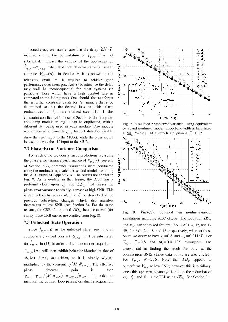
Fig. 7. Simulated phase-error variance, using equivalent baseband nonlinear model. Loop bandwidth is held fixed at 2 0.01LB T⋅ = . AGC effects are ignored. 0.95ζ = .
Fig. 8. ( )eVar θ , obtained via nonlinear-model simulations including AGC effects. The loops for MDD
and Mc are optimized for input SNRs of 1, 4, 15, and 17 dB, for M = 2, 4, 8, and 16, respectively, where at those SNRs we desire to have 0.8ζ = and 0.011/n Tω = . For
,M NV , 0.8ζ = and 0.011/n Tω = throughout. The
arrows aid in finding the result for ,M NV at the optimization SNRs (those data points are also circled). For ,M NV , 256N = . Note that MDD appears to
outperform ,M NV at low SNR; however this is a fallacy, since this apparent advantage is due to the reduction of
nω , ζ , and LB in the PLL using MDD . See Section 8.
878
we strive to have , 1L Vg = , which implies that we should
aspire to have ,SNR SNR dα α= . Thus, as a general rule, an
algorithm for deciding upon an appropriate SNRα would try, for example, to determine the latter either by (in order of increasing complexity): (a) using a worst case value (i.e. the value of ,SNR dα for the lowest SNR for which operation is desired), (b) using the last measured value of
NMl ,ˆ while locked (because , ,
ˆ[ ]M N SNR dE l α≈ ), or (c)
using some 0/SE N estimation technique (such as measurements on an auxiliary pilot signal) to estimate
,SNR dα . Methods (a) and (b) are quite simple to implement, though it is important to note that performance during acquisition is only partially addressed by using a constant SNRα , due to the fact that, since
,SNR dα varies with the SNR yet SNRα is constant,
, ,L V SNR d SNRg α α= will vary vs. the SNR.
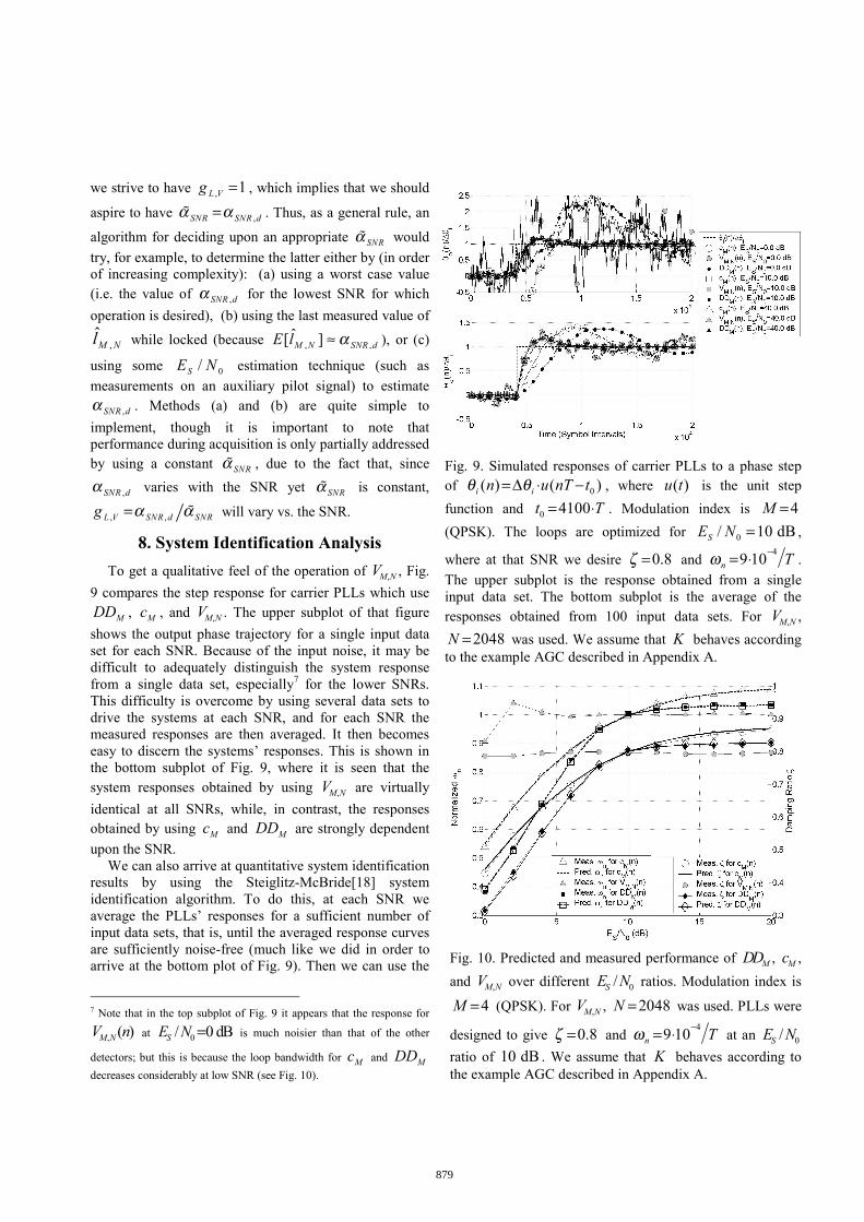
8. System Identification Analysis To get a qualitative feel of the operation of ,M NV , Fig. 9 compares the step response for carrier PLLs which use
MDD , Mc , and ,M NV . The upper subplot of that figure shows the output phase trajectory for a single input data set for each SNR. Because of the input noise, it may be difficult to adequately distinguish the system response from a single data set, especially7 for the lower SNRs. This difficulty is overcome by using several data sets to drive the systems at each SNR, and for each SNR the measured responses are then averaged. It then becomes easy to discern the systems’ responses. This is shown in the bottom subplot of Fig. 9, where it is seen that the system responses obtained by using ,M NV are virtually identical at all SNRs, while, in contrast, the responses obtained by using Mc and MDD are strongly dependent upon the SNR. We can also arrive at quantitative system identification results by using the Steiglitz-McBride [18] system identification algorithm. To do this, at each SNR we average the PLLs’ responses for a sufficient number of input data sets, that is, until the averaged response curves are sufficiently noise-free (much like we did in order to arrive at the bottom plot of Fig. 9). Then we can use the
7 Note that in the top subplot of Fig. 9 it appears that the response for
, ( )M NV n at 0/ 0 dBSE N = is much noisier than that of the other
detectors; but this is because the loop bandwidth for Mc and MDD decreases considerably at low SNR (see Fig. 10).
Fig. 9. Simulated responses of carrier PLLs to a phase step of 0( ) ( )=∆ ⋅ −i in u nT tθ θ , where ( )u t is the unit step function and 0 4100= ⋅t T . Modulation index is 4=M (QPSK). The loops are optimized for 0/ 10 dBSE N = ,
where at that SNR we desire 0.8=ζ and 49 10n Tω −= ⋅ .
The upper subplot is the response obtained from a single input data set. The bottom subplot is the average of the responses obtained from 100 input data sets. For ,M NV ,
2048=N was used. We assume that K behaves according to the example AGC described in Appendix A.
Fig. 10. Predicted and measured performance of MDD , Mc , and ,M NV over different 0/SE N ratios. Modulation index is
4M = (QPSK). For ,M NV , 2048N = was used. PLLs were
designed to give 0.8ζ = and 49 10n Tω −= ⋅ at an 0/SE N
ratio of 10 dB . We assume that K behaves according to the example AGC described in Appendix A.
879
Steiglitz-McBride algorithm upon the smoothed response in order to estimate nω and ζ . The results attained by following such a procedure are shown in Fig. 10. Also shown in Fig. 10 are curves of the expected ζ and nω as predicted in (28) for MDD and Mc . As was predicted in Section 7, ,M NV provides the desired damping ratio and
natural frequency over the entire input SNR range; MDD and Mc do not, and the parameters of their PLLs change according to (28).
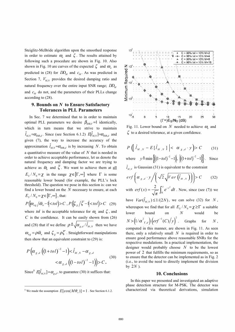
9. Bounds on N to Ensure Satisfactory Tolerances in PLL Parameters
In Sec. 7 we determined that to in order to maintain optimal PLL parameters we desire , 1SNR Vβ = identically, which in turn means that we strive to maintain
, ,M N SNR dl α= . Since (see Section 6.1.2) , ,ˆ[ ]M N SNR dE l α= and
given (7), the way to increase the accuracy of the approximation , ,M N SNR dl α≈ is by increasing N . To obtain a quantitative measure of the value of N that is needed in order to achieve acceptable performance, let us denote the natural frequency and damping factor we are trying to achieve as nω and ζ . We want to achieve them at all
0/SE N χ= in the range [ ],χ∈ Γ ∞ where Γ is some reasonable lower bound (for example, the PLL’s lock threshold). The question we pose in this section is: can we find a lower bound on the N necessary to ensure, at each
[ ]0/ ,SE N χ= ∈ Γ ∞ , that:
( )1n nP tol Cχω ω − < > , ( )1P tol Cχζ ζ − < > (29)
where tol is the acceptable tolerance for nω and ζ , and C is the confidence. It can be easily shown from (26)
and (28) that if we define , ,ˆ/d M Nlχρ α then we have
n nχω ρω= and χζ ρζ= . Straightforward manipulations then show that an equivalent constraint to (29) is:
( )( )(
( )( ))2
, , ,
2,
ˆ1 1
1 1
d M N d
d
P tol l
tol C
χ χ
χ
α α
α
−
−
+ − < −
< − − > . (30)
Since8 , ,ˆ[ ]M N dE l χα= , to guarantee (30) it suffices that:
8 We made the assumption [cos( )] 1eE M θ = . See Section 6.1.2.
( ), , ,ˆ ˆ [ ] M N M N dP l E l y Cχα− < ⋅ > (31)
where ( )( ) 2min 1 1 ,y tol −− − ( )( )21 1tol −+ − . Since
,M Nl is Gaussian (31) is equivalent to the constraint
( ), ,ˆ2d M Ne r f y V a r l Cχα ⋅ >
(32)
with 2
0
2( )
x terf x e dtπ
−= ∫ . Now, since (see (7)) we
have ,ˆ( ) 1/(2 )M NVar l N≤ , we can solve (32) for N ,
whereupon we find that for all 0/SE N χ= ≥Γ a suitable lower bound on N would be
( ) ( )22 1,1/ ( )dN erf C yα −
Γ> ⋅ . Graphs for N ,
computed in this manner, are shown in Fig. 11. As seen there, only a relatively small N is required in order to ensure good performance above reasonable SNRs for the respective modulations. In a practical implementation, the designer would probably choose N to be the lowest power of 2 that fulfills the minimum requirements, so as to ensure that the detector can be implemented as in Fig. 2 (i.e., to avoid the need to directly implement the division by 2N ).
10. Conclusions In this paper we presented and investigated an adaptive phase detection structure for M-PSK. The detector was characterized via theoretical derivations, simulation
Fig. 11. Lower bound on N needed to achieve nω and ζ to a desired tolerance, at a given confidence.
880
results, and system identification analysis. It was shown that the proposed structure allows for optimal PLL parameters to be maintained at any SNR at which the PLL can attain lock. Moreover, the detector has superior phase-error variance performance and has a compact implementation that is suitable for use within an FPGA or ASIC. Hence, the proposed structure has many immediate applications in M-PSK receivers.
Acknowledgments The author gratefully acknowledges the financial support provided to him by the National Sciences and Engineering Research Council of Canada (NSERC) through its Postgraduate Scholarship.
Appendix A: The AGC’s Operation
A.1 The Parameter K Obtaining a physical insight into the meaning of K is straightforward and should perhaps even be intuitively apparent to persons who have designed and built an M-PSK wireless receiver. To explicitly spell out this meaning, we assume that we are ideally locked (i.e.
0ω∆ = and 0eθ = ) and recall that throughout the paper we assumed for convenience and without loss of generality that 1pE = . We then have
( )( ) cos ( )n II n K n nTφ= + and ( )( ) sin ( )n QQ n K n nTφ= + .
Now, define the time-average operator • as
1
1( ) lim ( )2
N
N n N
x n x nN→∞ =− +
∑ . It is then easy to see
that:
02 2/ ( ) ( )SE NK I n Q n→∞→ + (33)
i.e. at high SNR we have that K is roughly the RMS (Root-Mean-Square) of the M-PSK signal. Now, to inject a little more real-world issues into the model, we know that samplers have a finite number of bits and the AGC’s job is, as already noted, to ensure that the samplers are not overdriven or underdriven. Consider, for example, a system which has 8-bit samplers, which give a range for
( )I n and ( )Q n of 127± . Let’s also assume that the AGC controls the input signal so that, to avoid sporadic overdriving of the samplers due to noise, the input signal’s RMS value is controlled to about 80% of the samplers’ dynamic range. Note that 8-bit samplers and 80% driving of the samplers are certainly real-world parameters. In terms of the signal model used in the paper (see Fig. 1) where unity gain samplers are assumed, it can
be seen that at high SNR the model of Fig. 1 applies with about 100K = (we rounded to 100K = . The exact number is 80% 127 101.6K = × = ). Let us now look at the situation at low SNR. Since we assumed for our model a constant SE , it follows that
0/ 0( ( )), ( ( )) SE NI QVar n nT Var n nT →→∞ . The AGC
still needs to control K so that the samplers are not
overdriven, and hence we must have 0/ 0 0SE NK →→ . In summary then, if b is the number of bits in the samplers (including sign bit) and the AGC attempts to control the RMS of the input signal to 100 r⋅ percent of
the samplers’ range, we have 0/ 0 0SE NK →→ and 0
1/ (2 1)SbE NK r −→∞→ ⋅ − . For example, for the 8-bit
samplers with 80% driving we discussed above, we have 8b= and 0.8r= , and the dynamic range of K is about
0 100K≤ ≤ . We can now easily see the problem with the implementation of the Mth-order nonlinearity NDA phase detector, i.e. Im[( ( ) ( )) ]M
Mc I n j Q n+ ⋅ , for which the phase detector implementation must accommodate the dynamic range of MK . Consider for example a 16-PSK receiver, i.e. a 16th order nonlinearity. With such an implementation and 0 100K≤ ≤ as detailed above, the PLL for Mc would have to accommodate at least the dynamic range of magnitudes of between 0 and
( ) 16 32max 100 10M
K = = . This would require the
output of a fixed-point lookup table to be
( )322log 10 1 107+ ≈ bits wide (!). Not only would this
be in itself unfeasible, but this means that the ensuing loop filter would also have to handle data that is 107 bits wide. Moreover, since the registers in the loop filter have typically many more bits than the input data width, this implies an entirely unrealizable loop filter. For the Mth power synchronizer, the only way to combat this explosion in logic resource usage is to artificially reduce K by discarding lower order bits of the samplers (thereby significantly worsening the effective sampler quantization), and to similarly discard the lower order bits of the output of the lookup table (thereby significantly limiting the dynamic range of the input I and Q signals that can be handled by the phase detector, and thus tightening the constraints on the AGC even more). Alternatively, floating-point implementations can be used; however, implementation of a floating-point
881
system in hardware (i.e. in an ASIC or FPGA) is always significantly more complex than implementation of a fixed-point system. Very similar problems afflict the implementation of the Mth-order nonlinearity NDA lock detector (see [1]). In contrast, for ( )Md n and ( )Mx n , the output of the
lookup tables is always in the interval [ ]1,1− , regardless
of K or M . Thus, with ( )Md n and ( )Mx n , a fixed-point lookup table with just an 8-bit output (quantization to 256 levels of the interval [ ]1,1− ) will usually be more
than sufficient, for any K and any M . As noted in Section 5.2, it then follows that a small dynamic range is needed for the lookup tables in Fig. 2. Again, as detailed in the previous paragraphs, this reduction in the necessary dynamic range has profound implications regarding the lookup table’s size, the size of the ensuing datapath and, in particular, the complexity of the loop filter. Finally, we could have just as easily adopted the convention that the binary point at the output of the samplers immediately follows the sign bit. For example, if the output of the sampler is 00000011b , this could
signify the value 3 or, alternatively, 3128 (if we think of
the binary point as being at the right of the sign bit, i.e. 0 0000011. b ). This decision is purely arbitrary and has no bearing upon the dynamic range considerations outlined above. Under the mathematically convenient assumption of the binary point being to the right of the sign bit of the sampler data, we have that 0 1K r≤ ≤ ≤ regardless of the number of bits in the sampler. This is the assumption made in this paper.
A.2 Understanding the AGC’s Operation
General analysis of AGC-induced effects is hindered by the fact that the constraints and parameters of AGC circuits are strongly dependent upon the specific communications system. It is thus, perhaps, less of a surprise that most contemporary synchronization texts ignore these effects (by assuming a constant 1K= ). This is the case, for example, in [6] and [13], which are some of the most comprehensive modern works on synchronization in wireless communications9. Here, we strive to attain an intuitive (rather than mathematically rigorous) understanding of the AGC’s operation. To that end, it is instructive to take a look at
9 Nonetheless, some treatment of AGC effects does exist. See for example [4] chap. 9 and [14] chap. 7, though the discussions there pertain to unmodulated carrier-wave synchronization.
the waveforms before and after the AGC. We assume as an example that our AGC attempts to control the waveform amplitudes at the input of the samplers so that the RMS value of the waveforms is 80% of the dynamic range of the samplers. We also assume, for simplicity, that the samplers’ full-scale input range is 1± volt, which means that our AGC tries to ensure that the pre-sampler waveforms have an RMS of 0.8 volt. We also make, for the purposes of the following demonstration, the same convenient assumptions as in the previous subsection, in particular, that the receiver is locked. Now, let as look at the pre-AGC (=post-matched-filter) and the post-AGC (=pre-sampler) waveforms at various SNRs. We shall look at the I -channel of a BPSK signal that has rectangular baseband pulses (remember that the signal has passed through a matched filter, so the signal waveform is now composed of the triangular pulses ( ) ( )p t h t⊗ ).
Fig. 12. Pre-AGC and post-AGC waveforms.
882
Fig. 12 shows the effects of the AGC upon the waveforms. In the bottom subplots, the dashed horizontal lines represent the samplers’ full-scale voltage. Of course, the AGC “sees” only the pre-AGC signal+noise waveform, and the samplers “see” only the post-AGC signal+noise waveform; the separation into separate signal and noise waveforms is only presented, courtesy of the computer simulation, for the benefit of the reader. As can be clearly seen in the graphs, the AGC insures that the signal+noise waveforms at the input of the samplers are such that the samplers are saturated infrequently, yet the 80% RMS driving level ensures that most of the dynamic range of the samplers is used at all SNRs. Clearly, had K not been reduced to accommodate for the noise power, the samplers would be saturated almost all the time, especially at low SNRs, as can be seen in the signal+noise waveforms before the AGC. Now, notice that the assumption made here is of a constant SE and a changing noise power. Put another
way, we assume that the 0/SE N changes because 0N changes. This is contrary to what happens in practice. In practice, the noise power is generally constant (we have
convention of a constant SE does not impact the analysis, and in fact simplifies it. The analysis is simplified because we can assume that true matched filters (with energy 2P SE E= ⋅ ) are present in the receiver. The receiver model adopted here is also the one used in most communications and synchronization texts (for example, see [6] and [13]). More importantly, the pre-sampler waveforms presented in Fig. 12 will be those that will indeed be encountered in practice, and, furthermore, the effective amplitude suppression factors in Fig. 6 are also those that will be encountered in practice. It is of paramount importance to realize that we are still assuming an ideal AGC, i.e. the example AGC circuit discussed above is assumed to be devoid of lag time and is assumed to control the RMS of the pre-sampler waveforms to precisely 80% of the samplers’ dynamic range. The assumption of a constant 1K= , though undertaken in the vast majority of synchronization texts, does not really describe an ideal AGC, but rather an atrophied AGC which operates within a system whose samplers have an infinite dynamic range and an infinite number of quantization bits. Clearly, the AGC discussed
here (though still “ideal”) is a much closer approximation of reality, as opposed to the assumption of a constant
1K= . The curve of K as a function of the SNR for our example AGC is given in Fig. 6.
References [1] Y. Linn and N. Peleg, “A family of self-normalizing carrier
lock detectors and ES/N0 estimators for M-PSK and other phase modulation schemes,” IEEE Trans. Wireless Commun., vol. 3, no. 5, pp.1659-1668, Sept. 2004.
[2] R. N. McDonough and A. D. Whalen, Detection of Signals in Noise, 2nd ed. San Diego, CA: Academic Press, 1995.
[3] J. G. Proakis, Digital Communications, 4th ed. New York: McGraw-Hill, 2001.
[4] Blanchard, Phase-Locked Loops Application to Coherent Receiver Design. New York: John Wiley & Sons, 1976.
[5] W. C. Lindsey and M. K. Simon, Telecommunication Systems Engineering. New Jersey: Prentice-Hall, 1973.
[6] H. Meyr, M. Moeneclaey, S. A. Fechtel, Digital Communication Receivers. New York: John Wiley & Sons, 1997.
[7] M. K. Simon, S. M. Hinedi, W. C. Lindsey, Digital Communication Techniques - Signal Design and Detection. Englewood Cliffs, NJ: Prentice Hall, 1994.
[8] M. R. Spiegel, Mathematical Handbook of Formulas and Tables. Singapore: McGraw-Hill, 1990.
[9] F. M. Gardner, Phaselock Techniques, 2nd ed., New York: John Wiley & Sons, 1979.
[10] W. P. Osborne and B. T. Kopp, “Synchronization in M-PSK modems”, Proc. ICC ’92, vol. 3, pp. 1436-1440
[11] W. P. Osborne and B. T. Kopp, “An analysis of carrier phase jitter in an M-PSK receiver utilizing MAP estimation”, in Proc. MILCOM ‘93, vol. 2, pp. 465-470.
[12] B. T. Kopp and W. P. Osborne, “Phase jitter in MPSK carrier tracking loops: Analytical, simulation, and laboratory results,” IEEE Trans. Commun., vol. 45, no. 11, pp. 1385-1388, Nov. 1997.
[13] U. Mengali and A. N. D’Andrea, Synchronization Techniques for Digital Receivers. New York: Plenum Press, 1997.
[14] H. Meyr and G. Ascheid, Synchronization in Digital Communications – Volume 1 Phase-, Frequency-Locked Loops, and Amplitude Control. New York: John Wiley & Sons, 1990.
[15] S. A. Butman and J. R. Lesh, “The effects of bandpass limiters on n-phase tracking systems,” IEEE Trans. Commun., vol. 25, no. 6, pp. 569 – 576, Jun. 1977.
[16] R. De Gaudenzi, T. Garde, V. Vanghi, “Performance analysis of decision-directed maximum-likelihood phase estimators for M-PSK modulated signals,” IEEE Trans. Commun., vol. 43, no. 12, pp. 3090-3100, Dec. 1995.
[17] R. E. Best, Phase-Locked Loops: Theory, Design, and Applications, 2nd ed. New York: McGraw-Hill, 1993.
[18] K. Steiglitz and L. E. McBride, “A technique for the identification of linear systems,” IEEE Trans. Automatic Control, vol. AC-10 (1965), p. 461-464.


![OUTER DERIVATIONS OF LIE ALGEBRAS · 1967] OUTER DERIVATIONS OF LIE ALGEBRAS 267 outer derivations is a linear sum of the outer derivations, which are obtained as in the first part](https://static.documents.pub/doc/80x56/5ec52027613ab73b287ddf89/outer-derivations-of-lie-algebras-1967-outer-derivations-of-lie-algebras-267-outer.jpg)


