A SELECTIVE ENCAPSULATION SOLUTION FOR PACKAGING AN OPTICAL MICROELECTROMECHANICAL SYSTEM by Amy Catherine Bowman A Thesis Submitted to the Faculty of the WORCESTER POLYTECHNIC INSTITUTE in partial fulfillment of the requirement for the Degree of Master of Science in Materials Engineering By _____________________________________ January 2002 APPROVED: _________________________________ Richard D. Sisson, Jr., Advisor Professor of Mechanical Engineering Materials Science & Engineering Program Head
Transcript
A SELECTIVE ENCAPSULATION SOLUTION FOR PACKAGING AN OPTICAL MICROELECTROMECHANICAL SYSTEM
by
Amy Catherine Bowman
A Thesis
Submitted to the Faculty
of the
WORCESTER POLYTECHNIC INSTITUTE
in partial fulfillment of the requirement for the
Degree of Master of Science
in
Materials Engineering
By
_____________________________________
January 2002
APPROVED:
_________________________________
Richard D. Sisson, Jr., Advisor
Professor of Mechanical Engineering
Materials Science & Engineering Program Head
i
ABSTRACT
This work developed a process to provide physical, electrical, and environmental
protection to the electrical lead system of an optical switch device. A literature review
was conducted to find materials and processes suitable to the stress-sensitive, high
voltage characteristics of many optical switch devices. An automatic dispensing dam and
fill process, and three candidate materials (two epoxy and one silicone) were selected for
investigation. Experimental and analytical techniques were used to evaluate the
materials. Methods applied included interferometric die warpage measurements,
electrochemical migration resistance tests (ECMT), thermal cycling, and finite element
analysis.
The silicone dam and fill system was selected based upon the results of die warpage and
electrochemical migration resistance tests. A modified, selective dam and fill process
was developed and preliminary reliability testing was performed. The paper provides
detailed instructions for successful encapsulation of the optical switch’s lead system.
ii
TABLE OF CONTENTS
Abstract ................................................................................................................................ i
Table of Contents................................................................................................................ ii
Table of Figures .................................................................................................................. v
Table of Tables ................................................................................................................viii
Table 6.1 Solutions to Key Processing Requirements ...................................................... 75
Table 6.2 Program Parameters for Selective Encapsulation Process................................ 84
1
1. INTRODUCTION
Microelectromechanical Systems (MEMS) are tiny electrically activated, mechanical
devices, ranging in size from microns to millimeters [1]. MEMS are typically fabricated on
silicon or glass wafers using adapted semiconductor processing techniques. The mechanical
components on MEMS devices are used in many common applications such as: pumping
within ink jet printer heads (Fig. 1.1 a), accelerometers to activate automobile airbags (Fig.
1.1 b), pressure sensors (Fig. 1.1 c), and a variety of sensors (chemical (Fig. 1.1 d), optical
(Fig. 1.1 e), electrical, or mechanical).
Figure 1.1 Examples of MEMS devices – a) SeaJet ink jet prinattached with FPC and printer head unit [2]; b) Analog Deviceaccelerometer; c) Accutire pressure sensor; d) Motorola gas se100-pixel IR sensor array [3]
e
d c
b
a
ter chip s nsor; and e)
2
1.1 Semiconductor Packaging
The technology used to manufacture and package MEMS devices is derived from the
processes developed for the semiconductor industry. By transferring these well characterized
and readily available materials and process technologies, the MEMS industry reduces the
time and cost of development [4]. Moreover, using the batch processing approach of the
semiconductor industry allows for low-cost, high volume manufacturing of MEMS devices.
A packaging hierarchy was established in the early days of mainframe computers to describe
the concept of different packaging levels [5]. Figure 1.2 shows the hierarchy of electronic
packaging from chip level to motherboard. Before packaging begins, the IC is diced from
the semiconductor wafer. Chip level interconnection refers to connecting the chip to the first
level package (e.g. solder bumps, or wires). A first level package refers to the IC,
encapsulated to provide mechanical/environmental protection, and its electrical contacts.
First level interconnection occurs when the first level package is connected to the second
level package. A populated printed circuit board (PCB) is an example of a second level
package. PCBs are ceramic or resin composite boards that interconnect active and passive
components onto a single board. Second level interconnection occurs when the second level
package is connected onto the third level package (e.g. the mother board). Higher levels of
packaging exist at the system level.
3
1st level packaging
2nd level packaging
3rd level packaging
Figure 1.2 First three levels of the tradit
Over the years, packaging hierarchy has evolve
MEMS. Many modern packages no longer fit d
its structure is useful in the understanding of g
the chip can be integrated directly into the sys
application in this work is a chip level package t
In order to choose a packaging solution, one
package, and the limitations of the chip and i
affect the packaging solution include: clo
1st level interconnection
Chip level interconnection
2nd level interconnection
ional packaging hierarchy [3]
d to fit the needs of new applications such as
irectly into the traditional hierarchy, although
eneral package functionality. In some cases,
tem. The solution proposed for the MEMS
o be integrated directly into the system.
must consider the required functions of the
ts application. Chip characteristics that will
ck speed, wafer thickness, dimensions,
4
environmental sensitivity, physical vulnerability, heat generation, and heat sensitivity. The
four basic functions performed by a package are to provide [6]:
1. Lead system (transfer/ connections),
2. Physical protection,
3. Environmental protection, and
4. Heat dissipation.
Examples of common lead systems are shown in Figure 1.3. The lead system is necessary to
allow electrical interconnection to the chip. It provides a pathway for electrical power and
read/write/signal data. For lead system design, it is important to keep in mind that signal
lines are more sensitive to electrical disruption (e.g. noise, cross-talk, leakage) than power or
ground lines. In fact, power and ground lines can be used to electrically shield signal lines
[7].
5
Figure 1.3 Plastic package configurations, featuring examples of common lead systems [8]
The completed package must provide physical protection to the semiconductor die as well as
the electrical connections. It should protect the brittle semiconductor die from harm such as
vibration or impact, and prevent breakage or crossing of the leads. In the case of the optical
switch, it must also protect the fragile mirror components on the surface of the device.
Environmental protection is necessary to keep the device free from harm by its surroundings.
The environmental protection requirements will vary depending upon the operating
environment and the needs of the device being packaged. For example, the optical switch is
sensitive to dust and particles, ionic contaminants, and moisture. A suitable packaging
solution will protect the device from any environmental factors that will cause the device to
fail, or reduce the lifetime of the device.
6
Heat dissipation is often required to remove the heat generated by powering the device.
Increasing the temperature of a device typically changes the electrical parameters, and may
eventually lead to permanent degradation and even failure of the device [7]. Temperature
changes also affect the physical construction of the device, due to CTE mismatch between
different materials. Figure 1.4 shows a heat fin and a heat spreader, two common methods
used to dissipate heat from electronic packages.
Figure 1.4 Heat fins and heat sinks - used in electronic packages to dissipate heat away from temperature sensitive components [9]
An enclosure is used to provide physical and environmental protection to the chip and the
chip level interconnects. The choice of enclosure depends upon requirements of the
application and reliability concerns. Common concerns include heat generation and
dissipation, chemical contaminants, mechanical stress, and electrical integrity [6]. Examples
of enclosures that address these concerns are polymeric encapsulation and polymer, metal,
ceramic, or glass sealed packages.
7
1.2 MEMS Packaging Challenges
The following quote from the National Research Council’s “Microelectromechanical
Systems: Advanced Materials and Fabrication Methods” summarizes the importance of
packaging to the MEMS industry:
“Packaging, which has traditionally attracted little interest compared to device and process development, represents a critical stumbling block to the development and manufacture of commercial and military MEMS. The imbalance between the ease with which batch-fabricated MEMS can be produced and the difficulty and cost of packaging them limits the speed with which new MEMS can be introduced to market. Expanding the small knowledge base in the packaging field and disseminating advances aggressively to workers in MEMS could have a profound influence on the rapid growth of MEMS.”
In most cases, semiconductor packaging technology cannot be directly transferred to MEMS.
The unique challenges of packaging MEMS are characteristic of the differences between
MEMS and typical semiconductor applications. Unlike ICs, MEMS often process non-
electrical signals (e.g. mechanical, optical, chemical). The package design must
accommodate the transmission of required electrical and non-electrical signals, while
protecting the MEMS from external influences that may be harmful to the device or
disruptive to the required signals. The micro components may be more adversely affected by
stress (e.g. pressure sensors or accelerometers), or subjected to more harsh environments than
ICs (e.g. chemical sensors). This deviance from typical processes and design rules tends to
reveal the limitations of current packaging technology, and may require the development of
new materials and processes [4]. A schematic representation of MEMS packaging
development is shown in Figure 1.5.
8
Figure 1.5 Block diagram of generic MEMS packaging requirements showing basic considerations of the package design [4]
The package design must accommodate the MEMS application, with respect to functionality
and operating environment. Interaction between the MEMS and their environment is often
required. Accordingly, the package needs to provide a protective enclosure with a “window
to the outside world” [10].
1.3 Polymeric Encapsulation
Polymeric encapsulation is a standard semiconductor process used to provide physical,
chemical, and electrical protection. Typically, the encapsulation process covers the entire
semiconductor surface. This thesis will focus on adapting a polymeric encapsulation process
to provide a “window to the outside world” to an optical MEMS (MOEMS) device.
There are three common types of polymeric encapsulation:
1. Transfer Molding (see Figure 1.6)
2. Potting
9
3. Glob Top Encapsulating
Figure 1.6 Schematic diagram of a transfer molding press [7]
1.3.1 Transfer Molding
Transfer molding is the most common IC encapsulation method for plastic packages [11]. It
was developed as a repeatable, high speed, high throughput process. In the transfer molding
process, a leadframe1 is loaded into the bottom half of a mold; a plunger forces molding
material from an auxiliary pot, through mold runners and gates, into a heated mold cavity;
pressure is held to be sure that the cavity is filled; the polymer resin is cured; the mold is
opened and the part ejected. An example of a selectively encapsulated, transfer-molded
package is shown in Figure 1.7. Table 1.1 highlights the advantages and disadvantages of
transfer molding.
1 A leadframe is a sheet metal connector framework used to connect the IC to the second level package.
10
Table 1.1 Advantages and Disadvantages of Transfer Molding Advantages Disadvantages
Low melt viscosity and “ram” pressure allow rapid encapsulation of many components simultaneously [12].
Parts must be able to withstand the elevated temperature and pressure of the transfer molding process. (This is a key problem for the MOEMS application.)
Encapsulated components have precise dimensions [12].
Filled resins used in transfer molding are highly viscous, threatening wire sweep, and necessitating high temperature and pressure [11].
Cycle times are fast [12]. The process tends to waste material, because material within the runners and pot are polymerized in the process, and cannot be re-used [11].
There is a uniform density of molded pieces [12]. The MEMS application requires a window to the outside world, which requires alteration of the standard transfer molding process and specialized equipment. High volume products, e.g. SensoNor’s pressure sensor have accomplished a signal window, but not an optically transparent window [13], [14]. See Fig. 1.7.
Process is very repeatable. High capital cost of mold and press [12].
Silicone plug provides a window to expose the pressure sensor
Leads for electrical interconnection
Figure 1.7 SensoNor SP28 tire pressure sensor - a transfer molded package with a silicone-filled window to expose the MEMS device [15]
1.3.2 Potting
Potting is the most simple encapsulation process [7]. The process involves placing the
electronic component into a container, pouring a liquid resin over the component to fill the
container, and curing the resin. The resin is a typically a thermoset polymer such as epoxy,
11
silicone, or polyurethane. The containers are made out of rugged materials, such as metal,
ceramic, or polymers. Potting results in rugged samples that are very conducive to
automated pick-and-place processes [7]. An example of a potted MEMS device is shown in
Figure 1.8. Conductive bumps for electrical interconnection
Injection molded outepackage
Figure 1.8 Seopening to ex
1.3.3 Glob Top En
Glob top encapsulati
used for chip on boa
The glob top provid
integrity of the wire
readily available and
There are single res
single resin process
wirebonds and cured
Exposed area for environmental exposure
r
Potted area in black
nsiron AH31 humidity sensor is a potted package, with an pose the sensor to the environment [16].
capsulation
on using epoxy resin is one of the most common IC packaging processes
rd (COB) applications. It is an inexpensive, easily automated process.
es physical and environmental protection, and helps to maintain the
s (see Figure 1.9 a). The process is well known and the materials are
well documented [7], [9], [11], [12].
in glob top processes and two-resin, “dam and fill” processes. In the
, the thixotropic glob top material is dispensed over the device and
(Figure 1.9 a). In the two-resin glob top process, a highly thixotropic
12
“dam” material is dispensed around the area to be encapsulated. Next, the “dam” is filled
with a lower viscosity material that covers the device and wirebonds (Figure 1.9 b).
a b
Figurresin
Like many p
sometimes re
modified to a
[19], [20], [21
wire bond ar
Figure 1.10 h
process (Fig.
Acsurdev
Bare devic
Figur
e 1.9 Two styles of glob top on ICs (a) single-resin pprocess
ackaging technologies, the transfer of the techno
quires alteration of the process. For example, th
ccommodate applications requiring an exposed dev
]. In order to allow a window for exposure, the glo
ea only, leaving the top surface of the MEMS ex
ighlights a “selective encapsulation” process that tra
1.9 b) to allow environmental exposure of MEMS de
Dispense dam material along inner and outer edges of wire-bonds
tive face of ice
Highly thixotropic dam material is deposited to protect the active area on device surface from the less viscous fill material.
wire-bonded e
e 1.10 Selective Glob Top Encapsulation Solution for
rocess; (b) two-
logy from ICs to MEMS
e glob top process can be
ice surface [3], [17], [18],
b top must be applied to the
posed to the environment.
nsfers the two-resin globtop
vices.
Dispense fill material inside of the dam area
High flow fill material is dispensed within the dam area, and allowed to flow around the delicate wire-bonds before curing.
MEMS Device
13
2. PROBLEM DEFINITION
The scope of this work is to investigate a particular MEMS packaging application.
Specifically, the thesis will provide an encapsulation solution for a MEMS-based, optical
switch device. The encapsulation process developed will provide electrical, physical, and
chemical protection to the delicate wirebonds and bond pads, while allowing a “window
to the outside world” for the optical switch. Figure 2.1 shows a flow chart summarizing
the steps that will be followed to develop the encapsulation solution.
Chapter 4: Review process and material options
Chapter 3: Define challenges of application
Chapter 7: Conclusions and Recommendations
Chapter 6: Develop Process Choose
Material
Chapter 5: Test materials to qualify them for basic requirements
Down-select process and materials
Figure 2.1 Thesis flow chart showing the process that will be used to develop an encapsulation solution
2.1 MEMS Device and Package
The MEMS device is used to optically switch between fiber optic telecommunication
channels. It consists of a 16 x 16 array of gold plated silicon mirror switches. Each ~
800 µm mirror is supported by two sets of gimbals (fabricated via a silicon etch process)
14
that allow the mirror to rotate along two axes. Electrodes beneath each mirror are used to
actuate an electrostatic charge, which deflects the mirror (see Figure 2.2).
Electrode pair
Figure 2.2 Two pixel, mirror switch in the Texas Instruments mirror array. The mirrors are shown as transparent. This array is used for an addressable electronic display, but it functions on the same concept as the telecommunications optical switch. [22]
The MEMS based optical switch device is a large, wirebond interconnected,
semiconductor die, housing electromechanical components. Parameters specific to this
device that will affect the encapsulation solution are a large die size (1 in.2 to 6.25 in.2),
sensitivity to stress (electromechanical device), high voltage (250 V), and high I/O
density (>1000 wirebonds). The mirrors on the device surface require optical exposure to
the environment (particularly within the wavelength range used for optical
telecommunications). Due to these limitations, it is critical that the encapsulant be kept
from the surface of the device, does not impart significant stress to the device, has a high
dielectric strength, and isolates the wirebonds, without causing wire sweep or breakage
(see Figure 2.3).
15
PCB for system level integration Large, stress
sensitive die
0.00125 in. Al wires require electrical isolation and mechanical protection
Application requires optical exposure
Figure 2.3 Overview of MEMS encapsulation concerns – The optical switch will require a low stress encapsulant that will meet the electrical requirements of the high voltage (~250 V), high wiring density (~1000 wirebonds over a 6.25 in.2 die) application.
After encapsulation, a cover plate and window will be sealed over the device, to protect
the exposed, active device surface (see Figure 2.4). The window will serve as
mechanical protection for the device. However, the encapsulant must protect the lead
system, withstand thermomechanical stress and high voltage, and provide corrosion and
electrochemical migration resistance to the wires and wirebond pads.
16
Anti-Reflection coated window mounted to cover plate to provide optical path and mechanical protection
PCB provides electrical interconnection from the MEMS to the system
Wire-bond area around device perimeter requires selective
2.2 Sel
Packagi
thermal
between
intercon
suscepti
Chapter
intercon
In the s
device
Aluminum coverplate provides mechanical protection to the device and wire-
A high dielectric constant is important for high-density applications, to prevent parasitic capacitances.
Process Results and Repeatability
Method of application, shelf life, pot life, moisture absorption, viscosity, wet ability, homogeneity, thixotropy
Changes in the material properties will affect processing.
Reliability CTE, modulus, shrinkage, moisture absorption, chemical resistance, adhesion to surfaces
Among other properties these significantly affect reliability.
3.1 Mechanical and Thermomechanical Stress
The encapsulant material must not exert high stress on the device. Stress leads to
warpage, which may be detrimental to the active components on MEMS devices. The
dependability of the device relies heavily on characterizing and accounting for possible
modes of warpage, and how that warpage affects the device [4].
For the optical switch application, warpage of the die makes it more difficult to align the
mirrors with optical fibers, and alters the mirror rotation angle necessary for switching. If
21
warpage exceeds the strength of the device passivation layer or of the die, it could crack
the passivation or the device itself. Other possible affects of warpage are lifting,
sweeping, or breaking of the wire bonds, and change in electrical and mechanical
properties, e.g. piezoresistance and resonant frequency [25]. The choice of encapsulant
material is a key decision that will significantly affect the amount of package warpage
[26].
A major contributor to the overall stress in many devices is thermo-mechanical stress.
Differences in the coefficient of thermal expansion (CTE) between substrate, silicon die
and encapsulant are a major reason for thermally induced stress [25]. The likeliness of
package warpage due to stress imposed by CTE mismatch increases dramatically with die
size. Thermal mismatch causes the materials to expand at different rates when exposed
to processing temperatures, inducing stress that causes the die to bend. The stress may
cause delamination of the encapsulant, or as the stress exceeds the ultimate tensile
strength (UTS) of the die, it will crack [27]. A low modulus of elasticity and good
adhesion to the die and substrate surfaces will enhance the encapsulant’s ability to
dissipate stress caused by thermal mismatch and reduce the risk of delamination,
respectively. The thermomechanical effects of cooling the encapsulant from its peak cure
temperature are demonstrated in Figure 3.2.
22
21
12
α = Coeficient of thermE = Young’s modulus
Figure 3.2 Warpage caused by cooldifferent CTE values
Large die, such as the one in this applica
than small die because of higher displac
between the encapsulant, MOEMS die
important. Matching the CTE will redu
curing, reflow, and other thermal process
MEMS devices are cure shrinkage, thermal
3.2 Electrical Performance
Specific electrical properties of interest are:
• Type and concentration of ionic con
• Volume resistivity, and
• Dielectric strength [29].
α1 > α2
Room Temperature
al expansion
ing two bonded mate
tion, are more affec
ement values. Th
, and packaging
ce thermomechanic
es. Other sources
gradients and moistu
taminants,
1
Unbonded 2
2 1
Bonded
Maximum Cure Temperature
1
2
E1 ~ E2
E1 << E2
rials with
ted by thermal mismatch
is makes CTE matching
components particularly
al stress induced during
of stress on encapsulated
re ingression [28].
23
The significance of electrical concerns (e.g. wire sweep, noise contamination, electrical
cross-talk, dendritic growth, and corrosion) increases with the density of the device’s
electrical contacts [11]. Fine wire pitch and high voltage bias increase the susceptibility
of the wire bonds and pads to electrostatic forces and electrochemical migration.
Electrochemical migration (dendritic growth as shown in Figure 3.3) can occur under
voltage bias, ionic contamination and humidity [5]. It leads to reliability failure when
the tiny dendrites grow to the next line, causing a short. The short pulls current very
quickly, and burns itself out. Electrochemical migration and galvanic corrosion is
avoided by keeping the package free of moisture and/or ionic contaminants.
a b Figure 3.3 Electrochemical Migration – (a) a schematthe electrochemical migration processes –[30]; (b) SEdendrites formed during electrochemical migration [31
An encapsulant material should be chosen that is low in i
moisture ingression. Moisture may lead to corrosion of the
are ionic contaminants remaining from processing or introduc
(e.g. chlorine or bromine) [32]. Corrosion due to ionic conta
ic representation of M image of ]
onic content, and prevents
device, particularly if there
ed by the glob top material
mination is a key reliability
24
issue with encapsulated electronic devices [33]. Most glob top manufacturers list type
and concentration of ionic contaminants (typically about 1 – 10 ppm) on the data sheets,
often highlighting “low ionic content” as a key feature of their products. In addition to
The encapsulant must provide electrical insulation to the wires, pads, and leads. It is
important to keep in mind that the optical switch will have a high voltage bias, ~250V.
The dielectric breakdown strength of the encapsulant is very important for high voltage,
high-density applications. High dielectric breakdown strength is important to prevent
leakage, arcing, and cross-talk between signal lines due to dielectric breakdown [11]. A
low dielectric constant would be important for high frequency devices with sensitive
signal lines, however, it does not apply to the MOEMS application.
3.3 Processing Considerations
The process refers to how the encapsulant is deposited onto the device and cured. An
initial set of process parameters must be defined to follow a few key objectives:
• Avoid wire damage (physical contact or wire sweep),
• Protect the device from electrostatic discharge (ESD),
• Avoid physical contact with the mirrors on the optical switch,
• Avoid contamination of the encapsulant or device,
• Ensure void free dispensing,
25
• Complete the dispensing within the time defined by the encapsulant’s pot life, and
• Do not exceed temperature limits of the device or package components.
After the initial set of process parameters is defined to fulfill the above objectives, the
process can be optimized.
Process repeatability is a key issue, particularly in the manufacturing world. The
process repeatability may be affected by the method of application, shelf life, pot life,
moisture absorption, and any change in material properties of the encapsulant.
Automated application methods make it much easier to apply the adhesive in a controlled
and repeatable manner. Automatic dispensing equipment (see Figure 3.4) controls
processing parameters such as temperature of the needle tip and substrate, dispensing
pressure, height of the needle above the substrate, velocity of needle movement, position,
and volume of material dispensed.
26
X, Y, Z gantry Dispensing valve
Heated work stage
Figure 3.4 Camalot 1818™ dispensing system
Encapsulation area and thickness are of particular importance to the optical MEMS
encapsulation solution. It is critical that the glob top be dispensed over the wirebonds
without contacting the delicate mirror devices on the surface of the die. Material
properties that will affect the area and thickness include thixotropy, wettability, and
homogeneity. The amount and type of filler material will also affect the encapsulation
area and thickness.
Voids in the encapsulation are an important electrical and reliability concern. Gas
enclosures may develop during the mixing of adhesive components; voids may form
during the cure cycle when the epoxy outgases; gas may be entrapped during dispensing,
e.g. in dead corners of the device; or wetting issues may contribute to void formation.
Voids are a source for moisture uptake, which may lead to a series of problems, e.g.
27
corrosion, delamination, electrochemical migration, or electrical cross talk [34]. A study
of the causes of voids in globtop found that materials cured at higher than recommended
temperatures have an increased tendency to form voids at the globtop-substrate interface
[35].
Another important processing consideration is the quality of the finished, encapsulated
surface. Properties and processes that affect the finished surface include viscosity, out-
gassing, fillers used, method of application, and cure schedule. Surface flatness is
important for components that are placed with vacuum pick-and-place equipment. It also
contributes to the physical appearance of the finished part, and to the ability to mask the
serial number, part number, and fiducials for automated pattern recognition systems or
automated optical inspection systems.
3.4 Reliability
“Reliability is the characteristic of an object that provides a required function whenever
such a function is sought. Failure to provide the function is a lack of reliability” [11].
Reliability can be estimated statistically as the probability that a component is still
functioning after operating for a specific amount of time. Key encapsulant parameters
affecting reliability are CTE, modulus, shrinkage, moisture absorption, chemical
resistance, and adhesion to surfaces [36].
Reliability tests are used to assess packaging components/systems. The tests involve
exposing the device to environmental stress according to a series of standards. Examples
28
of reliability tests include temperature cycling, highly accelerated stress test (HAST),
humidity bias life test and thermal shock (refer to Table 3.2). Test evaluations include
visual inspection, electrical, and mechanical testing [37].
Table 3.2 Typical Reliability Tests Used to Assess Glob-Top Assemblies Test Conditions Remarks Purpose
Temperature Cycling (JEDEC Standard JESD22-A104-A)
-55/+125oC
Transfer time < 1min.
> 10 min. dwell
Conditions vary per application;
At least 10 cycles
To accelerate thermal stress induced failures (dry test)
Thermal Shock (MIL-STD-883E Method 1011.9 Cond. A)
0/+100oC
Transfer time <10 sec
> 2 min. dwell
15 cycles To accelerate thermal stress induced failures (wet test)
Highly Accelerated Stress Test (HAST) (JEDEC Standard JESD22-A110-B)
130oC/ 85% R.H./
2.3 atm/ 96 hrs.
-5V, 0V, +5V bias To accelerate corrosion mechanisms and failures for early identification
Steady State Temperature Humidity Bias Life Test (JEDEC Standard JESD22-A101-B)
85oC/ 85% R.H.
1000 hr.
250 hr. test intervals
-5V, 0V, +5V bias
To accelerate corrosion mechanisms and failures for early identification
Resistance to Electrochemical Migration (IPC-TM-650 2.6.14.1)
Heat and humidity conditions vary
10 VDC bias 500 hr.
Conditions vary per application; Requires test specific board
To evaluate susceptibility to electrochemical migration
29
4. PROCESS AND MATERIAL SELECTION
There are many options to consider when choosing an encapsulant process and material
to fulfill a particular packaging requirement. Processing requirements/ limitations are an
integral part of the material selection process. Figure 4.1 is a flow chart, showing the
critical steps involved in choosing an encapsulant, and defining the encapsulation
process. The numbers in Figure 4.1 indicate the chapter and sections that will cover each
step of the material selection and process optimization.
Down-Select (4.3)
Select Encapsulant (5.3)
Evaluation Process Development (6)
Determine Available Materials (4.2)
List of Facility and Personnel Limitations
Method Consideration (4.1)
List of Device Performance Parameters
Testing andAnalysis (5.2 – 5.3)
Develop Experimental Matrix (5.1)
Define Procedure
Final Process Modification
Figure 4.1 Encapsulation process flow chart showing the critical steps toward choosing an encapsulant and defining an encapsulation process.
30
4.1 Method Consideration
Method consideration refers to the selection of an encapsulation process that is suitable to
the device. The method options will be narrowed by the device requirements, projected
cost of the device, the number to be manufactured, and the facility and personnel
limitations. The selection of a particular method will narrow the material options to those
appropriate to the process.
There are several common encapsulation methods as defined below [12]:
Encapsulate or “glob top”: Commonly used two ways: (1) the protection of an
electrical or electronic device with a plastic material; and (2) the forming of a thick
protective envelope (from 0.01 – 0.20 in. thick) around a device or component, applied
by dipping, spreading, or dispensing.
Pot: The placing of a device or component in a container (the “pot”), usually referred
to as a “can” if metal, or a “shell” if plastic. The container is then filled with the potting
material. The container thus becomes the exterior wear surface of the component or
device.
Cast: Same as pot except that the container is a temporary mold that is subsequently
removed and is usually reused. The insulation (potting material) thus becomes the
exterior wear surface of the component or device. The only difference between a cast
and a pot is removal of the container.
31
Conformal Coat: Application of a thin coating, usually 0.010 inches or less, most
often over a completed printed circuit (PC) board. Provides some environmental
protection and fixturing of the components on the board. Conformal coatings are applied
by spray, brush, or dip.
Mold: Placing a component or device in a metal mold, and forcing hot, molten plastic
into the mold. When cured, the mold is opened and the molded component or device is
ejected. The cycling times for molds are much faster than those for casts.
In order to select the appropriate encapsulation method, the device, facility, budget, and
personnel requirements and limitations need to be considered. The lists in Table 4.2
show the requirements and limitations of each.
The most suitable encapsulation method for the optical MEMS based device will address
the majority of the requirements and limitations listed in Table 4.1. Table 4.2 references
the compatibility of each encapsulation method to the relevant requirements and
limitations of the device, facility, budget and personnel.
32
Table 4.1 Requirements and Limitations Lists Device Requirements and Limitations
Must have optical exposure to the environment within the wavelengths used for fiber optic based telecommunication
Minimal die warpage (for optical alignment)
Minimal stress (device has stress sensitive components)
No contact should be made to the active area of the device
Encapsulant must provide mechanical support, electrical insulation and moisture barrier to 0.00125 inch diameter aluminum wire bonds
250 VDC voltage supply
20 years of functional reliability for qualified device
Available equipment:
Asymtec C-720M automatic dispenser with a pinch pump and an auger valve
Manual EFD dispenser
Budget:
No specific funding has been set aside for the encapsulation solution - standard prototype level budget restraints apply
Facility/ Personnel/ Budget Restrictions
Personnel/Safety:
Minimize health and safety risk to personnel and the environment
Table 4.2 Process Requirements vs. Encapsulation Methods Encapsulate
(“Glob Top”) Pot Cast Conformal
Coat Mold
Optical Exposure
Yes, with simple modification
Yes, with modification
Yes, with modification
Yes, if masked
Very difficult to achieve
Warpage/ Bow
Material dependant
Requires excellent CTE match
Requires excellent CTE match
Minimal Requires excellent CTE match
Minimal Stress
Yes, with attention to CTE and modulus
Requires excellent CTE match
Requires excellent CTE match
Yes Difficult to achieve
Wire Protection
Yes Yes Yes No Yes
Compatible with Available Equipment
Yes Requires a custom shell to allow optical exposure
Requires a custom mold to allow optical exposure
Yes – prototype only
No
Cost Expenditure
Minimal Minimal Minimal Minimal (prototype) High (mass production)
High
33
Table 4.2 compares the process requirements with each of the encapsulation systems.
The chart indicates that molding and conformal coating do not meet the basic
requirements for the MOEMS application. It would be very difficult to achieve optical
exposure with molding equipment. Although there are molding processes established to
allow mechanical exposure for small pressure sensors [14], they do not allow optical
exposure. The pressure sensor processes typically utilize a plug of silicone gel that
allows the transfer of mechanical signals, but would not be optically transparent [13],
[14], [15]. Conformal coating is a characteristically thin layer of material that would not
offer sufficient mechanical protection to the wire bonds. In addition, molding equipment
and production quality conformal coating equipment is not currently available at the
IntelliSense facility. Both molding and conformal coating equipment require a high
capital investment.
Potting and casting would require the design and fabrication of a custom shell or mold to
allow optical exposure. The mold would need to mask off the mirror array area from the
liquid, without physically contacting the delicate mirror area. Potting and casting
typically encapsulate the entire device, and are more suitable to small devices that are not
as susceptible to mechanical stress caused by CTE mismatch or shrinkage. Accordingly,
although a potting or casting process may be possible for the MOEMS device, both
would require substantial process modifications and extremely well matched
thermomechanical properties.
34
Through the process of elimination, glob top encapsulation has been selected as the best
match for the requirements and limitations of the MOEMS encapsulation process. Glob
top offers the most flexible and adaptable encapsulation method to allow optical exposure
and minimal stress, while protecting the delicate wire-bonds. Automatic dispensing
equipment can be used to define a glob top pattern that coats the wirebonds while
avoiding contact with the mirror area of the device. In addition, it is one of two methods
found to be compatible with available equipment.
A typical glob top is shown in Figure 4.2a. In the standard process, glob top is dispensed
over the top of the IC and wire bonds and cured to provide mechanical protection, and to
maintain the integrity of the wires. The process is well known and the materials are
readily available and well documented. Like many packaging technologies, the transfer
of the technology from ICs to MEMS often requires alteration of the process.
For the optical MEMS based application, the glob top process will be modified to allow
an optical opening for the device (see Figure 4.2b). The approach entails using a dam to
prevent the flow of encapsulant onto the active surface of the MEMS device, while
allowing protection of the metal areas (e.g. wires and bond pads). Potential areas of
concern for the glob top process modification include: wire sweep, increased mechanical,
thermal and thermomechanical stress, and process control (high precision is necessary, to
avoid covering device surface).
35
Dam material
Active surface of device
Fill material
a b
Figure 4.2 Comparison between (a) standard glob top used on ICs and (b) selective glob top encapsulation solution for MEMS device
4.2 Determine Available Materials
For the optical MEMS device, the choice of encapsulant is based upon its ability to
perform required functions. The optimal encapsulant will be able to provide mechanical,
electrical, thermal and chemical protection to wirebond interconnects. It must provide
such protection with minimal impact on the device parameters over an extended period of
time, and should be easily processed [29].
The most common encapsulant materials are epoxy-based [38]. Alternatives include
silicones, polyurethanes, phenolics and polyimides, among others [10]. In order to
choose an encapsulant, a literature review was performed to find the characteristic
properties of glob top options. Some of the key properties of the three most common
glob top materials are outlined in Table 4.3.
36
Table 4.3 Comparison of Encapsulant Properties* Epoxy Silicone Polyurethane
Adhesion Excellent Poor, often requires primer
Excellent
Mechanical protection
Excellent
Hardness ~ Shore D 80
Fair
Hardness ~ Shore A 47
Excellent
Hardness ~ Shore D 70
Thermal stability
Good
~ 200 oC
Excellent
~ 315 oC
Poor
~ 100 oC
Ionic Contaminants
Moderate
Cl- = <10 ppm
Na+ = <10 ppm
K+ = <10 ppm
Very Low High
CTE[10] Low
(10 - 70 ppm/ oC)
High
(150 - 1000 ppm/ oC)
High
(100 – 250 ppm/ oC)
Modulus [10] High
(3 – 10 GPa)
Low
(0.3 - 2 MPa)
Low – Medium
(2 – 16 MPa)
Electrical properties
Moderate
Resistivity~5x10¹⁶ ohm-cm
Dielectric Strength
~ 16 KV/mm
Excellent
Resistivity = 1x10¹⁵ ohm-cm
Dielectric Strength
~ 19.5 KV/mm
Good (poor at high temp.)
Resistivity ~ 4.2x10¹⁴ ohm-cm
Dielectric Strength
~ 15.1 KV/mm
Moisture Resistance
Good - Excellent
(0.0034% water absorption)
Excellent
(0.1% water absorption – refer to section 4.2.2 for explanation of silicone’s superior moisture resistance)
Poor
(2.1% water absorption)
*Quantitative values for CTE, electrical properties, moisture resistance, and hardness taken from MatWeb.com “The online materials information resource”, Copyright 1997-2001 by Automation Creations, Inc. MatWeb. The data have been taken from proprietary materials in the MatWeb database. Each property value reported is the average of appropriate MatWeb entries.
37
4.2.1 Epoxy
Epoxy was commercially introduced in 1947 [36]. It has a long history and has been
widely used, leading to a large database of information. Epoxies have been the most
common encapsulant material, and many formulations are available for glob top
applications through vendors such as Epoxy Technology, Dexter-Hysol, and Emerson
and Cuming [38].
Cure promoters or fillers may introduce ionic contaminants such as chloride to epoxy
materials during synthesis [29], [39]. The glob top specific epoxies have been carefully
formulated to contain very few ionic contaminants, have low dielectric constants and
high dielectric breakdown voltages.
Epoxies have excellent wetting characteristics, low permeability to water, and adhesion
to a wide variety of substrates under many environmental conditions [11], [10]. They
have high strength and are chemically resistant, providing good mechanical and chemical
protection [10], [11]. Epoxies are easy to process, suitable for all thermosetting
processing methods, and reproducible. They tend to have high dielectric breakdown
strength and volume resistivity.
Epoxy materials have a high modulus of elasticity [10]. They are known for high stress,
moisture sensitivity, and a short shelf life (can be extended if stored at low temperatures,
or as two separate components) [11]. The high modulus, high strength nature of epoxies
38
may cause warpage of the large MOEMS die. Warpage of the die will make the die more
difficult to optically align, and will alter the mechanical response of the active
components on the surface of the device. Epoxies tend to absorb moisture, which may
lead to reliability problems such as electrochemical migration, corrosion and popcorning
[40]. Electrochemical migration is a key concern for this high-density application, so
ionic contamination and moisture absorption would be particularly detrimental.
4.2.2 Silicone
Silicone is a low modulus alternative to epoxies. This low stress encapsulant has
excellent electrical properties, good chemical resistance, low water absorption, good
ultraviolet (UV) resistance, and high thermal stability (up to 315oC) [11]. The
combination of high thermal stability and a low modulus makes silicone superior to
epoxy in reliability tests such as thermal cycling and highly accelerated stress tests
(HAST) [39].
Superior silicone bonding to hydroxyl groups blocks adsorption of moisture films and
prevents conductive electrolyte paths between traces and modules [11]. This is a key
feature of silicones, and explains why they have performed very well under the highly
accelerated stress test (HAST) when used to protect silicon dies. The hydroxyl group
bond is the source of silicone’s moisture resistance. It is critical that contamination be
minimized for optimal hydroxyl group adhesion.
39
The disadvantages of silicones are the mechanical properties (e.g. lower adhesion and
strength than epoxies) and high CTE [33]. They are also less resistant to ion-
contaminated water than epoxies. Processability is also a key issue for silicones - they
tend to have batch-to-batch variations (not very reproducible); are very sensitive to
surface cleanliness; and can be poisoned by contaminants, inhibiting the cure process.
4.2.3 Polyurethane
Polyurethane glob tops are a second alternative to epoxies, and are less commonly used
for glob top applications. Like epoxies, polyurethanes require mixing a resin and a
hardener. However, their mix ratios are much more critical than epoxies, significantly
affecting material properties when ratios don’t follow specification [41].
Polyurethanes have good mechanical properties. Adhesion in lap shear and peel strength
are very strong. The hardness ranges from flexible to semi-rigid. This resiliency enables
them to accommodate differences in thermal expansion between materials and to absorb
mechanical shock [41]. Polyurethanes remain flexible at low temperatures, however their
physical and electrical properties are impaired at higher temperatures [12]. Use of
polyurethane should generally be limited to the –50 to 100o C range [10]. Within the
appropriate temperature range, polyurethanes have good electrical properties such as low
dielectric constant and dissipation factor and high dielectric strength and insulation
resistance [12].
40
One major difference between polyurethanes and silicones or epoxies is their moisture
sensitivity of the resin [9]. The urethane reacts preferentially with water, causing reduced
reactivity toward the curing agent, and sometime frothing (due to the evaluation of CO2)
[12], [41]. Other disadvantages of polyurethane include toxicity of the hardener
component, ionic contaminants, short pot life, and high CTE [12], [10], [41].
4.2.4 Filler Materials
Filler materials are often used to complement the properties of the encapsulant itself. The
choice of filler material depends on the requirements of the application. Advantages of
using fillers include: increased thixotropy, increased viscosity, reduced shrinkage,
improved toughness, improved abrasion resistance, reduced water absorption, increased
heat-deflection temperature, increased thermal and/ or electrical conductivity, and
reduced thermal expansion coefficient. Disadvantages of using fillers include increased
weight, increased dielectric constant, and added abrasiveness (may damage dispensing
equipment) [42]. Table 4.4 shows a comparison of some of the most common filler
materials.
Table 4.4 Common Fillers and Properties [42] Alumina Abrasion resistance, electrical resistivity, dimensional stability, toughness,
also list material property values that aid customers in choosing their most suitable
candidates within a particular group.
“Encapsulation of Electronic Devices and Components” by Edward Salmon gives an
excellent summary of how to approach the selection process for encapsulant materials.
The process begins with a review of the requirements and limitations of the device and
facility (refer to Table 4.2). In his book, Salmon makes the point that the best material
for the job may not be available or practical. The selection process is a balance between
device performance, facility and personnel capabilities, supply availability, and cost.
43
4.3.1 Epoxy Selection
Supplier tables, supplier’s applications engineers, and electronics industry literature were
consulted to select epoxy encapsulant materials to be evaluated in this work. The
candidates selected were chosen based upon their availability, cost and likeliness to fulfill
the specifications described in Table 4.2. Epoxy selection was narrowed down to two
dam and fill systems (see Table 4.6). It is important to have compatible materials for the
dam and fill, so that cure cycles, CTE, and shrinkage properties are compatible, thus
reducing thermally induced stress.
Table 4.6 Material Properties of Selected Epoxy Encapsulants CTE
(ppm/oC) Hardness
(Shore D)
Ionic Content (ppm)
Volume Resistivity
(ohm-cm)
Water Absorption
(wt. %)
Epoxy 1 - Dam and Fill
(Silica used as a filler to increase thixotropy of the dam)
40 89 N/A 5 x 10¹⁵ 0.1
Epoxy 2 -Dam
20 90 Cl- <10
Na+ <10
K+ <10
NH4+ <10
3.3 x 10¹⁴ < 0.4
Epoxy 2 - Fill
20 90 Cl- <10
Na+ <10
K+ <10
NH4+ <10
N/A N/A
Epoxy 1, is pertinent because it had been used to selectively encapsulate an IR micro
system device (see Figure 4.3). In that system, the epoxy had been selected for superior
44
electrical properties, including resistance to electrochemical migration [3]. Epoxy 1 is an
easily accessible, general purpose, two-part epoxy, with good adhesion. It has a low
viscosity, and is compatible with machine dispensing. The material’s low viscosity is
characteristic of a fill material. However, amorphous silica filler can be used to increase
thixotropy and dimensional stability, so that it can also be used as a dam.
Figure 4.3 An IR micro system device that has been selectively encapsulated with Epoxy 1
Both Epoxy 2 materials were designed for use as a system, having compatible material
properties. The Epoxy 2 dam and fill are single component epoxies, minimizing lot-to-
lot variation and voiding caused by air introduced during the mixing process. This
system features low stress (low CTE), high purity, and low ionics. The fill is intended for
situations where the number and density of the wire bonds require an especially easy
flowing glob top. Low stress and low ionics are key features that will minimize die
warpage and electrochemical migration between the dense wires and bond pads on the
device.
4.3.2 Silicone Selection
As in the epoxy selection process, supplier tables, supplier’s applications engineers, and
electronics industry literature were consulted to select silicone encapsulant materials to
45
be evaluated. Again, candidates selected were chosen based upon their likeliness to
fulfill the specifications described in Table 4.2, availability, and cost. Two silicone
candidate systems were selected for the study. Silicones are much more compliant than
epoxies, so thermal mechanical issues are less of a concern. Silicones are available
individually, rather than in dam and fill systems. A comparison of their properties is
shown in Table 4.7. Ionic content and water absorption values were not available for the
silicones.
Table 4.7 Material Properties of Selected Silicone Encapsulants
CTE (ppm/o C)
Hardness
(Shore A)
Volume Resistivity
(ohm-cm)
Silicone 1- Dam (1-part) N/A 39 7.7 x 10¹⁴
Silicone 1- Fill (2-part) 300 45 1.0 x 10¹⁴
Silicone 2 – Dam and Fill (2-part) 200 75 > 1014
Silicone 1 dam is a readily available, one-component, non-slumping silicone material
formulated for use with corrosion-sensitive electrical equipment. It is a general-purpose
sealant and adhesive, easily dispensed with automatic equipment. It has the consistency
of a paste, which renders useful as a dam material.
Silicone 1 dam reacts with moisture in the air to cure. As described in Section 4.2.2, the
key to silicone’s moisture resistance is the bonding of hydroxyl groups that block
adsorption of moisture films, preventing conductive electrolyte paths between traces and
modules [11]. Device cleanliness is more critical for silicone encapsulants than the
46
absorption of water. Contaminants may block the hydroxyl group bond between the
silicone and surface of the device, metallization, and wirebonds.
The Silicone 1 fill data sheet claims that it has excellent adhesion. Unlike most silicone
encapsulants that are available, it requires no primer. It has long shelf and pot lives (24
months and > 3 days, respectively), and a low viscosity (1500 cP), making it useful for
the high wire density of the MOEMS application.
Silicone 2 has very low shrinkage (0.002 cm/cm), is non-corrosive, and claims high
reliability of its encapsulated assemblies. However, the material requires a primer for
adhesion. The primer adds an additional step in the encapsulation process, which would
decrease the ease/ speed of manufacturability. Accordingly, it was not pursued further.
47
5. QUALIFICATION AND RELIABILITY TESTING
Considerations for qualification of a material include cost, availability of materials,
reproducibility of the process, and reliability of the finished product [7]. The goal of
qualification testing is to identify the capability of the encapsulants to function according
to the requirements of the device [9]. Qualification tests include accelerated tests to
indicate the reliability of different materials. Figure 5.1 is a flow chart, showing the steps
involved in qualifying an encapsulant material for the MOEMS application.
Testing and Analysis (5.3)
Choose Test Methods Based on Requirements (5.2)
Develop Experimental Matrix (5.1)
Select an Encapsulant
Figure 5.1 Process flow for qualifying and selecting an encapsulant material
5.1 Develop Experimental Matrix
The objective of this study’s experimental matrix, is to select a set of experiments that
will aid in the down-selection of a material for MOEMS development. This study does
not address testing extensively to qualify the materials at a manufacturing level. In
selecting a material, data is taken from many sources, such as test data from material
suppliers, qualification data for similar products, and accelerated test data from
subassemblies and materials [12]. [9] summarizes a plastic encapsulation qualification
process that will cost-effectively assure that the item will meet requirements:
“The qualification process includes the following steps:
48
• Determine the aim of the specific qualification process in terms of required nominal reliability.
• Determine the environmental and operational stresses at the upper and lower design limits. Typical qualification stresses include time and special dependent electrostatic discharge, current, and voltage.
• Identify the likely failure mechanisms and modes (during manufacture, system assembly, transportation, storage, and service), and determine the relevant acceleration models and factors.
• Conduct tests and collect the necessary failure data to assess reliability and durability of the product. Typically this involves accelerated testing. A sample size is chosen to achieve the qualification goals; complete electrical measurements may be required before and after each qualification test to uncover any failures.
• Interpret data, and report results and conclusions with feedback for continuous improvement.”
According to the qualification process plan outlined in [9], there are a few specific
questions that will help direct the qualification process to a suitable set of tests and
acceleration models. Table 5.1 answers the first three bullets in the qualification
process guideline, setting the stage to determine the most relevant set of tests. For
more detailed specifications and requirements, please refer to Chapters 2 and 3.
49
Table 5.1 Planning Qualification of MOEMS Encapsulant Material Electrical Mechanical/
Thermomechanical Processing
Goal of qualification process (nominal reliability)
- Minimize electrochemical migration
- Volume resistivity > 1 x 10¹⁴ ohm-cm
- Dielectric breakdown strength > 300 V/mil
- Minimize warpage and stress
- Encapsulant needs to be kept away from mirror area
- Fill material has to infiltrate the dense wirebonds without wire sweep or breakage
Environmental and operational stress
- 250 V operating bias
- Humidity
- Ionic contaminants
- Operating temperature range of -40oC – 85o C for telecommunication devices [9]
- Handling and exposures during the assembly process and test
- Viscosity and flow pressure of uncured fill material
• Dam material was deposited onto Pyrex die following the pattern shown in Figure
5.6, and cured according to the manufacturer’s suggested cure schedule. The
volume of each dam was kept uniform between encapsulant systems by
measuring the dispense rate of the dam material in grams per second, and
plugging the value into equation 5.1:
V = R/(ρ ⋅ v) (5.1)
Where:
V = Volume dispensed [cm3/in]
R = Dispense rate of material for specific needle, pressure, and auger
valve rotation speed [g/s]
ρ = Density of encapsulant material [g/cm3]
v = Velocity of dispense needle for specific needle, pressure, and auger
valve rotation speed [in/s]
60
Figure 5.6 The pattern used to dispense dam material onto Pyrex die mimics the selective encapsulation pattern that will be used to protect the wirebonds on the MOEMS device.
• A Zygo interferometer was used to evaluate the change in die bow caused by the
dam materials.
• Fill material was deposited onto the Pyrex die inside of the dam material as shown
in Figure 5.7, and cured according to the schedule assigned by the manufacturer
of the material. Equation 5.1 was used again, to keep the volume of material
dispensed uniform between samples.
Figure 5.7 The pattern used to dispense fill material onto Pyrex die mimics the selective encapsulation pattern intended to be used to protect the wirebonds on the MOEMS device.
61
• A stereoscope was used for optical inspection. Post-cure inspection revealed that
the epoxy dams spread out more than the silicone dam, resulting in larger contact
areas the silicone system.
• A Zygo interferometer was used to measure the change in die bow caused by the
fill materials.
• The encapsulant systems were compared to show which material caused the most
die warpage. The graph in Figure 5.8 summarizes the results of the measurements.
Die Warpage Experiments
-20
-10
0
10
20
30
40
50
60
70
80
90
a - x b - x a - y b - y a - x b - x a - y b - y a - x b - x a - y b - y
Sample - Axis(a = first sample; b = second sample; x = short axis of die; y = long axis of die)
Peak
to V
alle
y M
easu
rem
ent A
cros
s D
ie (m
icro
ns)
#3 -Fill
#3 - Dam
#2 - Fill
#2 - Dam
#1 - Fill
#1 - Dam
Figure 5.8 Zygo interferometer surface profile results, showing the change in die bow after encapsulant materials were cured onto Pyrex die
In Figure 5.8, a positive peak reflects a concave die bow, with the encapsulant side facing
the top. The results show that System 3, having the highest CTE and lowest modulus,
had the least amount of warpage. Although the same volume was used for each dam and
fill system, each took a different shape. The shape was dependant upon the thixotropy
and viscosity of each of the materials. The silicone dam in System 3 was the most
62
thixotropic, yielding to a tall, narrow dam topography. The System 2 dam was the least
thixotropic, and spread out, resulting in a higher contact area between the dam and glass
test die.
5.3.2 Electrochemical Migration Resistance Test and Result
The procedure used to evaluate electrochemical migration resistance was based upon
IPC-TM-650 2.6.14.1 Electrochemical Migration Resistance Test. In summary, IPC-TM-
650 2.6.14.1 specifies the use of a test board with a comb pattern of conductor lines
(Figure 5.4), having line widths and spaces of 0.0125 in. [0.318 mm]. The test method
specifies that the conductor lines be left as untreated, bare copper, unless another surface
finish is part of the evaluation. The method gives several temperature and humidity
options. Testing is performed under a 10 VDC voltage bias, after a 96-hour stabilization
period of temperature and humidity exposure.
The standard procedure was adapted to better represent the electrical field of the
MOEMS application. Changes made to the standard test simulated the fine pitch and
high voltage of the MOEMS application. The adapted comb pattern had a series of
0.004 in. [0.102 mm] copper conductor lines and spaces. Four comb patterns were used
per test coupon (see Figure 5.9a). The lines of the first comb pattern were covered with
solder mask, to be used as a reference. The remaining three had openings left in the
solder mask to simulate the Cu/Ni/Au wirebond pads that will be encapsulated (see
Figure 5.9b). The voltage bias was increased from 10VDC to 100VDC, to simulate the
high voltage used for this application. This amounts to a three-fold increase in line
63
density and 10-fold increase in bias. The lowest temperature/humidity combination of
40o C and 93% relative humidity was used to prolong the test long enough to have a
measurable comparison between systems.
a
Figure 5.9 (a) Electrochemical migration test coupon usedencapsulant systems’ ability to prevent dendritic growth unbias, at elevated temperature and humidity (b) encapsulantcover the exposed area on the ECMT coupons
The electrochemical migration testing was performed at Robisan
have the capability of simultaneously testing 64 comb patterns
resistance (SIR) meter set-up to run the test in an environmen
typically uses the IPC test to evaluate solder mask materials, wh
coating over conductor lines on printed circuit boards. IntelliSe
have a SIR meter, or a chamber capable of controlling temp
Although, it is possible to maintain a humid environment usi
introduce ionic contaminants to the system, potentially accele
migration.
b
to test the der a voltage pattern used to
Laboratory, Inc. They
on a surface insulation
tal chamber. Robisan
ich provide a dielectric
nse does not currently
erature and humidity.
ng salt solutions, they
rating electrochemical
64
Figure 5.10 shows the electrochemical migration test (ECMT) sample coupons hooked up
to the power source, in the test chamber. The coupons are hard-wired to the power
source using PTFE-insulated solid conductor wire, as specified in the test standard. They
are hanging from a rack that maintains spacing between the specimens, so that airflow is
parallel to the direction of the specimens in the chamber, per IPC-TM-650 2.6.14.1.
100 VDC power supply
Chamber maintained at 40o C/ 93% R.H.
Figure 5.10 Electrochemical migration resistance test set-up, showing test coupons inside of the environmental chamber, connected to a 100 VDC power supply [45]
Susan Mansilla, Technical Director of Robisan Laboratory described the typical criteria
necessary for a solder mask to pass IPC-TM-650 2.6.14.1. Typically, the resistance
measurement between conductor lines should be a minimum of 5x10⁸ ohms, with no
65
dendritic growth between lines, or the resistance drop between 0 and 500 hr. should not
exceed one decade. It is also very important that there is no delamination of the
insulating material after the ECMT is complete. Figure 5.11 compares the resistance
measurements taken before and after the 500-hour bias period in the environmental
chamber.
Figure 5.11 Comparison of the average insulation resistance (IRavg) of samples before and after the 500-hour voltage bias/ environmental exposure
The test results reflect the change in the average resistance of 64 sets of comb structures
after 500 hours of exposure to 100VDC bias, 40oC and 93% relative humidity. The
resistance values for the solder mask control, open bond pads, and System 3 increased
after the 500 hours of exposure. This is a common result for electrochemical migration
testing, and may be an affect of having surface volatiles burn off during the
environmental exposure [45]. All samples, including the open bond pads, performed well
Electrochemical Migration Test Results
4.13E
+10
3.46E
+11
1.36E
+11
6.61E
+09
3.72E
+10
5.33E
+10
1.09E
+10 1.2
7E+1
0
1.59E
+11
9.13E
+10
1.E+09
1.E+10
1.E+11
1.E+12
Solder mask control Open bond pads System 1 System 2 System 3
Res
ista
nce
(ohm
s)
0 hours
500 hours
66
under the adapted IPC-TM-650 2.6.14.1 test, indicating that the original printed circuit
boards were clean and had very little ionic contamination. System 1 showed the worst
performance, as the resistance dropped by slightly more than one decade, indicating
failure.
Visual inspection after the ECMT was limited to the uncoated area outside of the
encapsulation. Upon examination of the 64 line sets, two burns were found on control
channels, and three areas were found with dendritic growth between lines, outside of the
coated area. Figure 5.12 shows burn and dendritic growth examples. The dendritic
growth (Figure 5.12a) causes electrical shorts, which burn out under the applied voltage,
causing burns like the one in Figure 5.12b.
Figure 5.12 Optical examination of the 64 line sets after 500 hours exposure to 100 VDC bias, 40oC and 93% relative humidity revealed a few examples of (a) dendritic growth between metallized lines and (b) burns on the control lines
67
5.3.3 Optical Inspection
A stereoscope was used to inspect both die warpage and electrochemical migration test
samples after the encapsulant materials were cured. Optical inspection at 60X
magnification revealed voids in the two-component Fill 1 and Fill 3 materials (see Figure
5.13). No voids were found in the single-component Fill 2 material. Fills 1 and 3 were
hand mixed, two-component materials. The voids would most likely be avoidable
through improved mixing and outgasing techniques.
Figure 5.13 Photomicrograph of voids found in the silicone Fill 3 – may be avoidable through improved mixing and outgasing techniques
5.4 Finite Element Analysis
Finite element analysis (FEA) is a mathematic modeling technique that may be used to
complement laboratory experimentation to optimize a process. FEA requires updating
with laboratory results, so that the mathematical model is based on actual system
behavior. FEA may be used to select materials or optimize processes. A 3-D, quarter,
FEA was built to simulate the dam and fill encapsulation around the MOEMS device
[44]. The assumptions included: no heat convection in the thermal symmetric boundary;
68
a 30oC reference temperature; and the bottom of the substrate was fixed in the z direction.
The dam and fill materials were assumed to be soft elastic (Poisson’s ratio<0.5) to
simplify time-dependant and temperature-dependant visco-elastic behavior. The load
cycle was assumed to be stress free at the maximum cure temperature. The meshed
model is shown in Figure 5.14.
Figure 5.14 Finite element model used for analyzing the thermomechanical behavior of dam and fill materials [44]
The model showed that the dam and fill materials add stress to the assembly and cause
warpage, as shown in Figure 5.15.
69
Figure 5.15 Finite element model showing magnified deformation characteristic of the MOEMS die after the dam and fill process [44]
The model was used to compare the three dam and fill systems with regard to die
warpage. Dam and fill System 3 showed the least amount of die warpage. Although the
warpage values differ, the trend correlates with the results of profilometry experiments
discussed in section 5.3.1.
Different encapsulant geometries were input to the finite element model, to see the effect
of dam and fill shape on die warpage. The study showed that shape formed by the dam
and fill materials (refer to section 5.3.1) had a significant impact on the warpage. Die
bow can be reduced by minimizing the surface area covered by the encapsulant.
Accordingly, the more thixotropic dam materials (e.g. the silicone dam used in System 3)
have a geometric advantage, because they maintain a narrow profile. In addition, the
study showed that warpage could be further reduced by leaving the corners of the die, the
area of highest stress, free of encapsulant material. The open cornered pattern showed a
70
significant reduction in the finite element model’s warpage. Figure 5.16 shows the
Figure 5.16 Performance Comparison Between Dam and Fill Systems [44]
5.5 Select an Encapsulant
Table 5.4 shows the matrix used to down-select an encapsulant. The table demonstrates
each encapsulant system’s ability to meet requirements evaluated through experimental
testing. Each encapsulant system is rated with a value from 1 (poor) to 5 (excellent) for
the specifications that were evaluated in testing, and the system with the highest score
was selected for processing experiments and thermal cycling.
71
Table 5.4 Encapsulant Selection Matrix Minimal
Warpage Electrochemical Migration Resistance
Resistance to Voids and Cracking
Total Value
System 1 (Epoxy)
1 3 3 7
System 2 (Epoxy)
1 4 3 8
System 3 (Silicone)
5 5 4 14
All of the dam and fill encapsulation systems performed reasonably well for the
electrochemical migration testing. The test results for System 1 were just below the
typical criteria for IPC-TM-650 2.6.14.1, which is still fairly impressive when
considering that the voltage bias was ten-fold higher than in the standard test. The
ECMT results were favorable for dam and fill encapsulation systems 2 and 3.
The interferometry/surface profile results showed that System 3 is a considerably better
candidate than either System 1 or 2. The change in surface profile after curing System 3
was an order of magnitude lower than either of the other systems, so low that it was
within the 5 µm accuracy of the Zygo interferometer. Systems 1 and 2 caused
significant warpage of the die after cure. These results can be attributed to three
characteristics that gave System 3 a thermomechanical advantage over the other systems:
1. Low Young’s modulus of elasticity (3 – 5 MPa for System 3 versus 7000 – 9000
MPa for Systems 1 and 2),
2. Low cure temperature (85o C for System 3 versus 125 - 150o C for Systems 1 and
2), and
72
3. Geometry of dam and fill after cure (high thixotropy of System 3 minimized
contact area between encapsulant and die).
System 3 showed a significant superiority over the other two dam and fill systems in
thermomechanical interaction with the Pyrex test die. Thermomechanical FEA results
also suggested that system 3 would minimize encapsulant-induced die warpage,
particularly with the open-corner pattern. Accordingly, system 3 was the only one
chosen for processing experiments.
73
6. PROCESS DEVELOPMENT
The encapsulation process refers to how material is selectively deposited onto the device
and cured. There are several key requirements that make the process a success.
Referring back to Chapter 5, Table 5.1, the nominal requirements include infiltrating the
dense wirebonds without wire sweep or breakage, and avoiding physical contact with the
mirror area. Other important objectives are:
• Protect the device from electrostatic discharge (ESD) – High wiring
density and the design of the MOEMS make the device vulnerable to
ESD.
• Avoid contamination of the encapsulant or device – Particle contamination
could cause mechanical and optical failure of the MOEMS. The MOEMS
and encapsulation could electrically fail from ionic contamination,
whereas organic or inorganic contamination could decrease the adhesion
or inhibit the curing of the silicone material.
• Ensure void free dispensing – Voids entrapped in the encapsulation could
cause reliability issues for the device.
• Complete the dispensing within the time defined by the encapsulant’s pot
life - If the pot life has been exceeded, the properties of the material start
to change, impacting, e.g., the flow characteristics, curing, and adhesion of
the encapsulant.
74
• Keep within temperature limits of the device or package components -
Exceeding the temperature limits can introduce stress, degrade materials,
and cause damage to the device.
6.1 Processing Experiments
An automatic dispenser was used for the processing experiments. The parameters that
need to be defined for the process are e.g., geometry, valve type, needle gage, back
pressure, needle speed, and height of needle. The process can also be enhanced by
setting delays at the beginnings of the dispensed lines to allow the material time to flow,
and sweeping back along the line to remove strings of material. Table 6.1 highlights
specific actions considered in the process development to satisfy the above requirements.
75
Table 6.1 Solutions to Key Processing Requirements
Requirement Action
Infiltrating the dense wirebonds without wire sweep or breakage
Avoid needle contact with the wires by choosing a small needle size and maintaining sufficient height above bond pads and distance from wires)
Choose a low viscosity fill material
Heat may be applied to the needle and/or chuck to lower the viscosity of some materials
Avoid physical contact with the mirror area Avoid needle contact with mirror area
Choose a thixotropic dam material
Ensure that the dam prevents the fill material from entering the mirror area
Protect the device from electrostatic discharge (ESD)
Maintain a common ground between device and handler
Use static dissipative laboratory supplies
Ionize non-conductive materials that are in the area of the device, to avoid charge build-up
Avoid contamination of the encapsulant or device Perform work in a cleanroom environment
Keep the device covered and sealed in an ESD bag when not in use
Wipe the dispenser tip clean before dispensing
Ensure void free dispensing Be careful not to entrap air while mixing two-part adhesive systems
Apply a vacuum to de-gas materials before using
Purge the needle before dispensing
Complete the dispensing within the time defined by the encapsulant’s pot life
Be aware of the pot life, and work within the limits (count-down clocks can be used for the timing)
If the encapsulant’s consistency begins to vary, replace it with fresh material
Keep within temperature limits of the device or package components
Choose appropriate materials with low cure temperatures
To cure, use the lowest temperature recommended by the manufacturer
76
6.1.1 Defining the Selective Encapsulation Pattern
The initial set of processing experiments served to define the pattern of the selectively
encapsulated area. The first experiment defined an inner dam area on the device, halfway
between the wirebond pads and the edge of the mirror array (Figure 6.1a). The outer dam
was just outside of the bond pads on the printed circuit board. The advantage of this
arrangement was to keep the dam at a maximum distance from both the mirror array and
the wire bonds, to help avoid physical contact. The dam process was successful,
however, the fill material infiltrated to the mirror area along the channels for conductor
lines connecting the mirrors to the wirebonds. In order to prevent the capillary forces
from drawing the fill material into the mirror area, the dam was re-positioned to the
wirebond trench area (Figure 6.1b). The re-positioned dam seals the channels and fills
part of the trench, as shown in Figure 6.2. It has been found to cause no problems if the
dam covers the stitch area of the wirebonds. However, the dam must not cover the wire
loop. The dam material’s thixotropy would inhibit the impregnation of the wires and
cause voiding. Finally, the repositioned dam minimizes the area of MOEMS covered by
the encapsulant, thus, lowering the stress introduced by the encapsulation materials.
After experimentally specifying an encapsulation area, the pattern was further refined
through finite element analysis. The finite element simulation predicted a reduction in
die stress by reducing the amount of material, particularly at the corners of the die (refer
to Figure 5.10) [44].
77
Mirror area
Wirebond trenches
Inner Dam
Figure 6.1 Two positions for innetrenches and mirror array does narea along interconnect lines; (b)trenches to block fill material fromcontact between the dispensing ne
Mirror area
a
o
Wirebond trenches
Inner Dam
b
r dam (a) midway between wire bond t keep fill material from entering mirror dam moved to inner edge of wire bond conductor lines, while avoiding
edle and delicate wirebonds
78
needle
wirebond channels for conductor lines
dam
MOEMS
Figure 6.2: Schematic cross section of the dam position – The position was optimized to seal off the channels for the conductor lines, and prevent fill material from flowing into the mirror area.
6.1.2 Refining the Process
Selecting the pattern for the encapsulation is only the beginning of the process
development. The dispenser parameters, e.g. valve type, needle gage, needle height,
needle speed, have to be adjusted to accommodate the material properties and pattern
shape. The height of the dam material is dependant upon the material’s thixotropy, and
height, gage and speed of the needle.
An auger valve was selected to dispense the thixotropic dam material. Auger valves
combine back-pressure with a rotating auger to dispense the materials in a well
controlled, repeatable manner. In order to avoid contact between the needle or dam
material and the wires, the dam material should be deposited with the finest needle
capable of dispensing the viscous material. Pneumatic valve pressure and auger speed
have to be adjusted to allow the dam to flow consistently from the needle. Line width
can be controlled by the needle speed and height.
79
A pinch pump was selected for use with the fill material. The pinch pump features a
mechanical stop, which holds the dispensing tube shut until sufficient back-pressure is
applied. The pinched tube is advantageous to use with low viscosity fill materials, to
keep them from dripping at the needle tip. The auger valve is unnecessary for fill
materials, because they do not require fine volume control.
Further refinements include adjusting the dispenser parameters to avoid, e.g.,
inconsistency, widened lines, and line gaps. Examples of typical processing challenges
are illustrated below.
Wavy, inconsistent lines occur when the material is not flowing from the needle
consistently. This effect, shown in Figure 6.3, is often seen when material flowing from
the needle tip does not make immediate contact with the substrate. Possible solutions
include:
• Lowering needle height to allow the material to make contact with the
substrate;
• Slowing needle speed to dispense more material along the line;
• Increasing auger speed or back-pressure to dispense more material along the
line.
80
Figure 6.3 Wavy, inconsistent lines often occur when the needle is too high for the volume of material being dispensed.
Flat, widened lines are an indication that the distance between the needle and substrate is
too narrow for the volume of material being dispensed. Possible solutions include:
• Increasing needle height;
• Increasing needle speed so less material is dispensed over the line;
• Decreasing auger speed or back pressure.
Strings, as shown in Figure 6.4, indicate that the material is sticking to the needle after
the line has been dispensed. Possible solutions include:
• Programming the dispenser to have the needle backtrack over the lines,
sweeping the material from the needle. Backtrack parameters include
distance, height, and speed.
• If the backtracking does not work, the needle can be programmed to touch
down onto the substrate in a non-critical spot to break-off the string.
81
Figure 6.4 Strings occur when excess material sticks to the needle after the line has been dispensed.
Figure 6.5 shows an open line. Opens in the line indicate that the material is not flowing
from the needle, or that enough material has not been dispensed to make effective
contact. If they occur at the beginning of the line, it is likely that the material is still
working its way down the needle. If they occur in the middle of a line, it is likely that
there are voids in the syringe. Possible solutions include:
• Set the program to delay movement at the beginning of the line, to allow time
for the material to exit the needle tip and contact the substrate before motion
begins.
• If the opens occur in the middle of the lines, the material in the syringe may
contain voids, and should be de-gassed.
82
• If it is apparent that the material is flowing, but not sufficiently to make
effective contact, the needle speed should be slowed or the needle height
should be lowered.
• Check the valve and needle tip for clogged material. The valve should be kept
clean at all times. If the needle tip is clogging, switching to a conical tip or
using a larger needle may suffice to avoid material back-up.
Figure 6.5 Opens in the lines often occur when the material is not flowing adequately from the needle tip.
After adjusting the process, and making the refinements described above, the dispenser is
programmed to make a smooth consistent dam line, like the one shown in Figure 6.6.
83
Figure 6.6 Properly dispensed dam lines feature a smooth, rounded surface, no gaps, and no strings
The fill material is not required to hold tight geometric tolerances. After meeting the
electrical, mechanical, and thermo-mechanical specifications, the fill needs only to
remain void free, cover the wirebonds, and infiltrate between wires and within the entire
dammed space without overflowing the dam.
Upon completion of experiments to meet the specifications for both dam and fill,
dispensing programs were finalized. The dam program makes three passes over the
pattern. Each pass is at a consecutively higher needle position in order to match
wirebond height, maintain a narrow wall within the wirebond trench, and avoid contact
with the wire loops. The program parameters are shown in Table 6.2. Dispensed dam
and fill were cured according to manufacturer’s recommendations i.e., 24 hours at room
temperature for the dam material, and 3 hours at 85oC for the fill material.
84
Table 6.2 Program Parameters for Selective Encapsulation Process Backtrack Valve Settings Pump
Type Needle Size (gage)
Needle Height (in.)
Delay (s)
Needle Speed (in/s) Height
(in.)
Speed (in/s)
Length (in.)
Pressure (psi)
Auger Speed (rpm)
Dam Layer 1
Auger 25 0.018 0.5 0.37 0.018 0.2 0.4 10
3
Dam Layer 2
Auger 25 0.023 0.5 0.40 0.023 0.2 0.4 10
3
Dam Layer 3
Auger 25 0.031 0.5 0.41 0.031 0.2 0.4 10 3
Fill Pinch 18 0.040 0.1 0.16 0.043 2.0 0.1 16 N/A
6.2 Temperature Cycling Test
The process described in Table 6.2 was implemented for the selective encapsulation of
test devices. The availability of test devices was limited by the high cost of the MOEMS
devices and packaging materials. The devices available for experimentation were five
rejected parts, which failed inspection due to cracks, high die curvature, electrical failure,
or low device yield. Selective dam and fill encapsulation was performed according to the
parameters described in Section 6.1.
Temperature cycling tests were performed on the best three out of five low yield devices.
Prior to encapsulation, the devices were optically inspected for cracks. Devices 1 and 2
had no cracks, Device 3 had a small crack at one edge as shown in Figure 6.7.
85
Figure 6.7 One of the three thermal cycling test devices had a small crack (as shown) prior to encapsulation.
Temperature cycling tests were performed in accordance with the JEDEC test standard
JESD22-A104. The temperature was performed between two chambers held at –40oC
and 125oC, respectively. The samples were subjected to 10 cycles with 10 minutes soak
time and 1 minute transfer time between chambers.
After testing, the devices were optically inspected at 50X magnification. Electrical
testing was not performed, because the devices were low yield, rejects. Device 1 had no
visible cracks. Devices 2 and 3 had cracks as shown in Figure 6.8.
86
a b
Figure 6.8 Cracks found in Devices after thermal cycling (a) Device 2 and (b) Device 3
The results of temperature cycling tests were inconclusive. Device 1 survived thermal
cycling without cracking. The crack found in Device 3 grew from another crack that had
been found prior to temperature cycling. This indicates that the crack was due to a stress
concentration within the device, not necessarily related to the encapsulation. The crack
found in Device 2 was indicative of temperature cycling failure, however, not necessarily
caused by the encapsulation materials. Several packaged, non-encapsulated MOEMS
prototype devices have had cracking problems. Typically, cracks occur in devices from
the same lot, and are likely an indication of inferior material quality or processing
parameters. The devices used in testing were, by definition, substandard.
87
7. CONCLUSIONS AND RECOMMENDATIONS
Although optical switches ultimately require hermetic packaging for long-term reliability,
selective encapsulation offers several benefits to MOEMS applications. The non-hermetic
solution offers a simplified, low-cost, quick-turn alternative, ideally suited to the
research, development, and prototyping of MOEMS devices. A non-hermetic prototype
package results in cost and time-savings by allowing parallel development of the
MOEMS device and its final, hermetic package. In addition, selective encapsulation
techniques may improve cost and manufacturability of MOEMS packaging solutions. By
hermetically sealing a window directly to the active area of the device, selective
encapsulation may be used to protect interconnects in the final MOEMS package.
7.1 Results and Conclusions
A literature review was performed to select candidate processes and materials for
selective encapsulation. Process techniques and material properties were evaluated to
compare their ability to meet the MOEMS device’s primary requirements:
• Optical exposure to the mirror array of the device;
• Minimal thermomechanical, thermal, and mechanical stress on the device;
• Mechanical protection of the 0.00125 inch wirebond interconnects;
• Prevention of electrochemical migration and corrosion between wirebond pads;
and
• Prevention of dielectric breakdown.
88
Automatic dispensing of a selective dam and fill encapsulation pattern provides a process
suitable to protect MOEMS wirebonds, minimize stress, and provide optical exposure to
the mirror array of the device (refer to Table 4.3 for a comparison of processes). The
dam and fill process was chosen based upon literature review, device requirements, cost,
and equipment availability. Three candidate sets of dam and fill, two epoxies and one
silicone, were selected for analytical and experimental evaluation. Methods applied
included interferometric die warpage measurements, electrochemical migration tests, and
finite element analysis. Processing experiments were performed after material selection.
Thermal cycling and visual inspection were used to evaluate processing results.
7.1.1 Material Selection
The literature review revealed that epoxy and silicone materials were the best candidates
for the selective encapsulation process. Epoxy was selected because it is the most
common glob top material, offering many formulations. Properties that made epoxy an
attractive candidate include:
• Low CTE (compatible with silicon die),
• Excellent wetting and adhesion,
• Low water permeability,
• Low ionic contaminants (through specific formulations), and
• Ease of processing.
Silicone is a popular alternative to epoxy-based encapsulants, offering different
properties that make it suitable to the MOEMS application, including:
89
• Low elastic modulus,
• High dielectric strength,
• Low ionic contaminants, and
• Low cure temperature.
Two epoxy dam and fill systems and one silicone system were selected for further
evaluation, based upon device specifications, facility requirements, availability and cost.
7.1.2 Analytical and Experimental Evaluation
An experimental matrix was developed to choose relevant tests to evaluate dam and fill
materials. Packaging industry standards were included in the matrix, shown in Figure
5.2. Tests were selected from the matrix based upon their ability to provide information
on whether the encapsulants were able to withstand 250 V operating bias, and humidity
and temperature fluctuations. Selected tests included:
1. Optical inspection to evaluate voiding;
2. Interferometer profilometry to measure warpage;
3. Resistance to electrochemical migration to evaluate reliability under a voltage
bias and exposure to humidity (per a modification of IPC-TM-650-2.6.14); and
4. Temperature cycling to accelerate thermal stress induced failure after processing
(per JEDEC JESD22-A104).
A finite element analysis was performed to complement the experimental work, and to
aid material selection and process development.
90
Experimental and analytical results showed that die bow is minimized by choosing
materials with low modulus of elasticity, low cure temperatures, and by optimizing the
geometry of the encapsulation area. Specifically, the encapsulation area should be
limited to the wirebond area, avoiding areas most susceptible to stress concentration such
as the device corners. Figure 7.1 shows a schematic of the final dam and fill
encapsulation pattern.
Wirebond Trenches
Mirror Array
Silicon Die
PCB Fill
Dam
Figure 7.1 Final dam and fill encapsulation pattern
A modification of the electrochemical migration resistance standard was used to evaluate
the encapsulant materials under a high electrostatic field, reflecting the operating voltage
and device line spacing. Results showed that one of the two epoxy systems failed, by
having a resistance drop greater than one order of magnitude.
91
Of the three candidate systems, the silicone was the only one to pass both warpage and
electrochemical migration resistance experiments. The low modulus of elasticity and low
cure temperature of the silicone system resulted in minimal die warpage, an order of
magnitude lower than either epoxy system. Accordingly, it was the only encapsulant
selected for processing experiments.
7.1.3 Processing Experiments and Evaluation
Protection of the mirror area of the MOEMS device can be achieved through careful
positioning of the dam material. The dam material needs to be sufficiently thixotropic to
hold its shape after dispensing through a fine needle. Several fine strips of dam material
may be deposited on top of one another, to obtain a narrow dam with sufficient height to
protect the wirebond area. The dam should be dispensed inside of the wirebond trench,
because it is less susceptible to the capillary forces than the fill material. In so doing, the
watery fill material is prevented from flowing along electrical lines to the mirror array.
An auger valve and fine needle combination allow accurate and repeatable dam
dispensing results. The geometry of the fill material does not require as much precision
control, so a pinch pump and large needle is sufficient. The fill material may be
deposited in a single pass. The final dispenser program parameters are defined in Table
6.2. This recipe can be used to successfully encapsulate the lead system of the MEMS-
based optical switch device. Figure 7.2 shows the results of the final process.
92
Figure 7.2 Fi al Dam (a) and Fill (b) results ba
Optical inspection r
encapsulants were cu
area. Optical inspec
The fact that one o
cracking is a positive
7.2 Recommenda
The post-processing
Acoustic microscopy
Components IPC/JE
reveal whether there
the device/encapsula
sections may be hel
present outside of the
n
evealed several voids at the surface of th
red. This suggests that there may be mo
tion also revealed cracks in two of the thre
f the three devices survived temperature
indication for the silicone encapsulant mat
tions
voids found during optical inspection req
(Acoustic Microscopy for Non-Hermetic
DEC J-STD-035) is commonly used for p
are voids under the surface of the plastic
nt interface. In addition, optical exami
pful to reveal voids, but require critical a
cross-sectioned areas.
e fill material, after the
re voids in the wirebond
e thermal cycled devices.
cycling without visible
erial.
uire further investigation.
Encapsulated Electronic
ackaging applications, to
encapsulated area, and at
nation of polished cross
nalysis, as voids may be
93
There are several options available to help prevent voids from occurring:
1. After mixing components, add steps to the de-gassing process, to include vacuum
and back-pressure cycles, rather than a single vacuum step; or
2. Use pre-packaged, single component materials to avoid trapping air during the
mixing process;
3. Leave room at the edges when dispensing the fill within the dam area, so that
trapped air may escape; and
4. Pull vacuum on device after fill is applied, prior to cure (again, a vacuum/back-
pressure cycle may enhance the removal of trapped gas).
In addition to addressing the void problem, the selective encapsulation process requires
further reliability characterization. The testing performed in this work is suitable to a
prototype/ development scale package. In order to qualify the encapsulant materials for
inclusion to a production/ manufacturing level package, extensive tests would be
required. In particular, thermal cycling and long term reliability tests need to be
performed on more encapsulated devices, preferably devices that have satisfied
inspection requirements and can be electrically characterized.


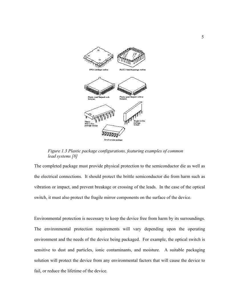


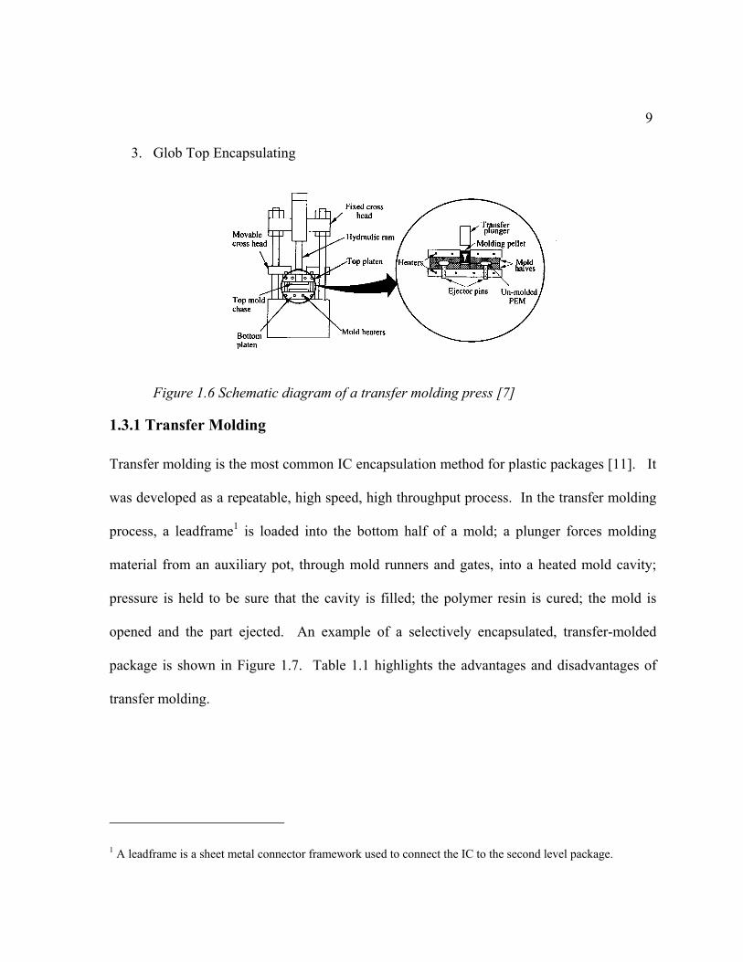


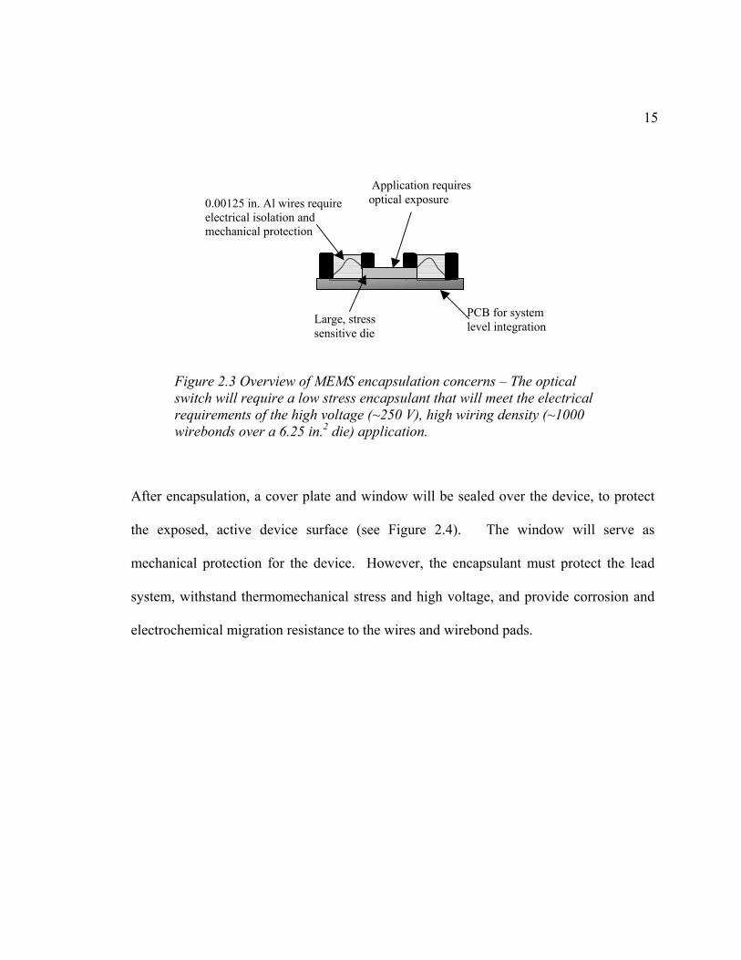


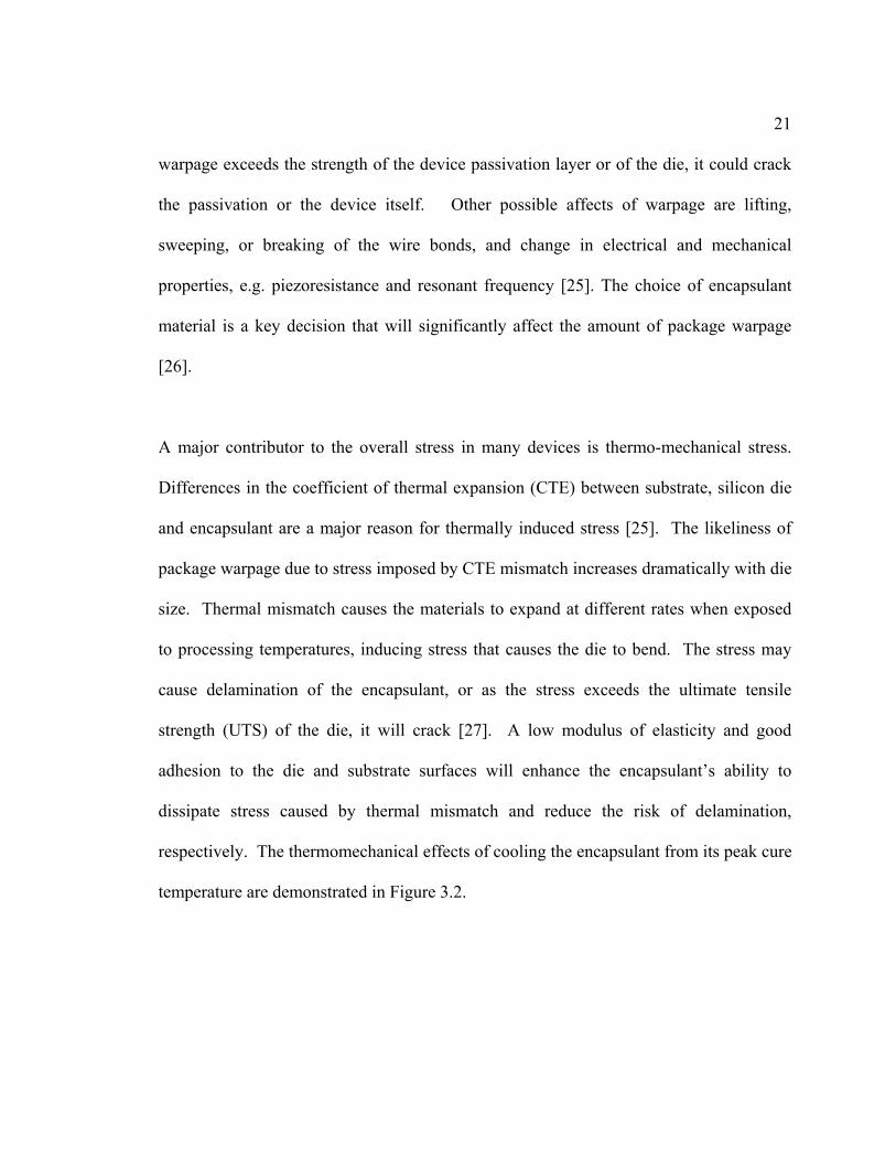


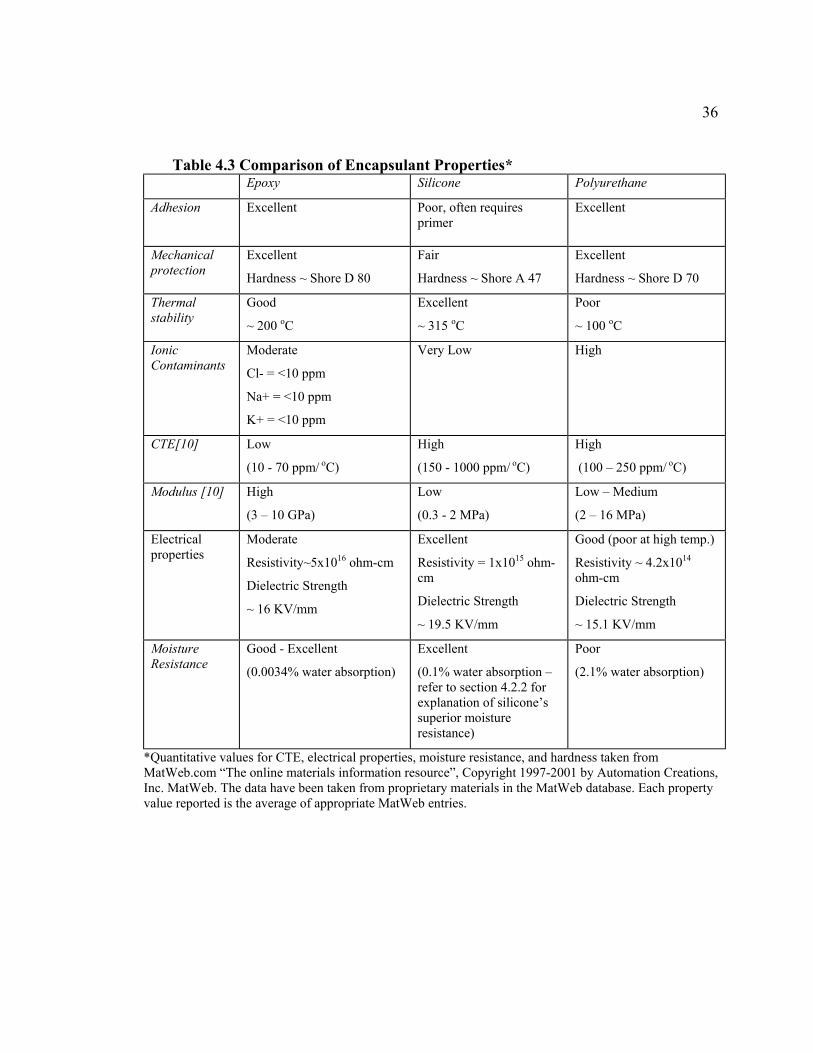
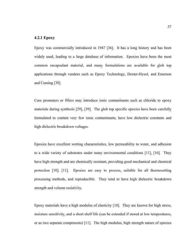


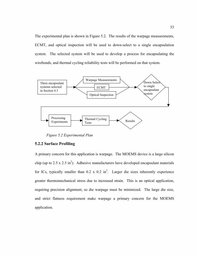
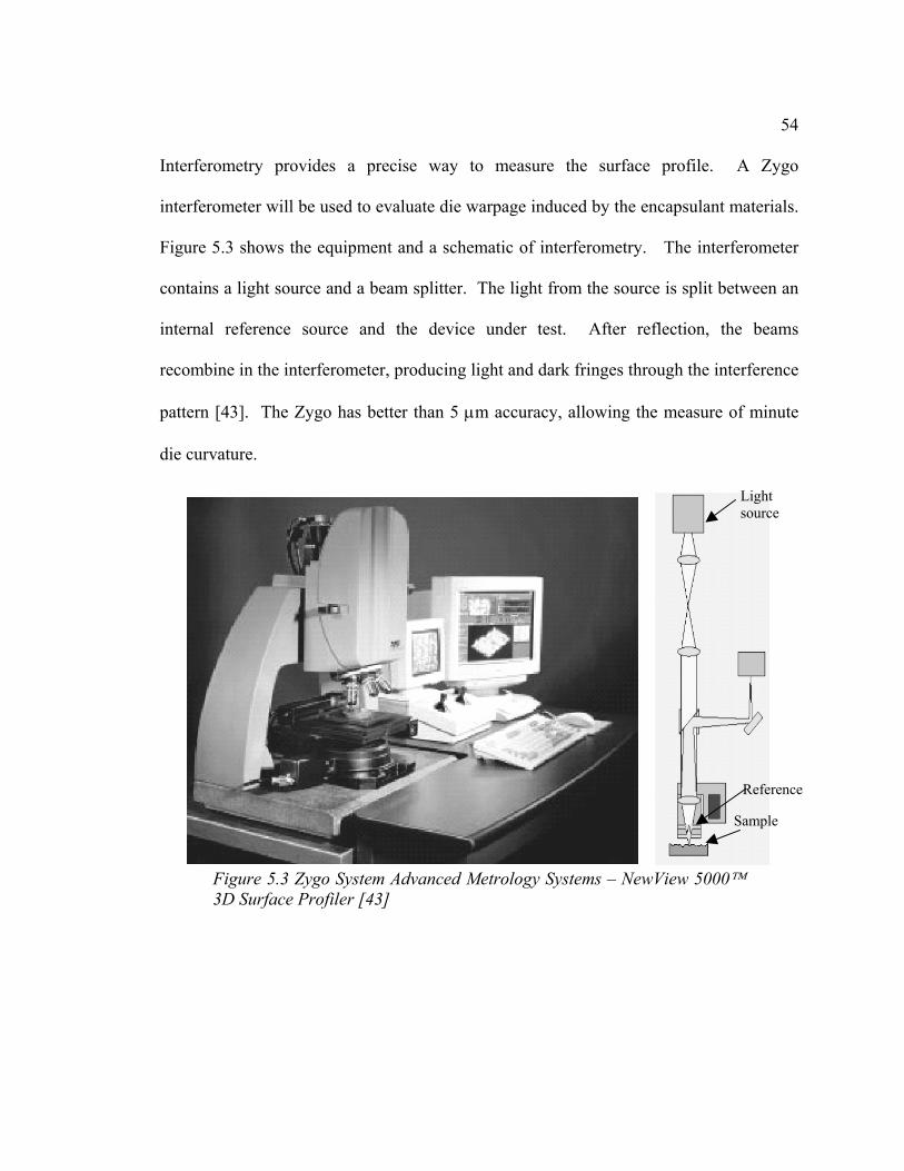
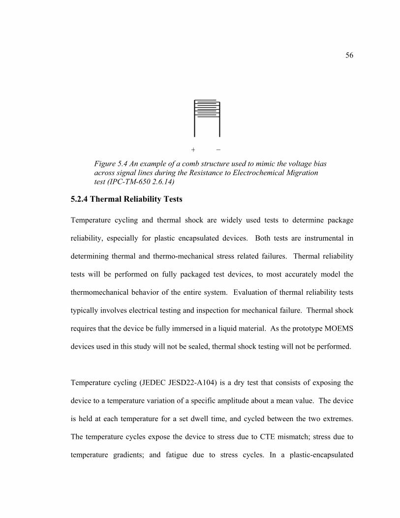


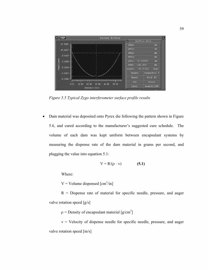

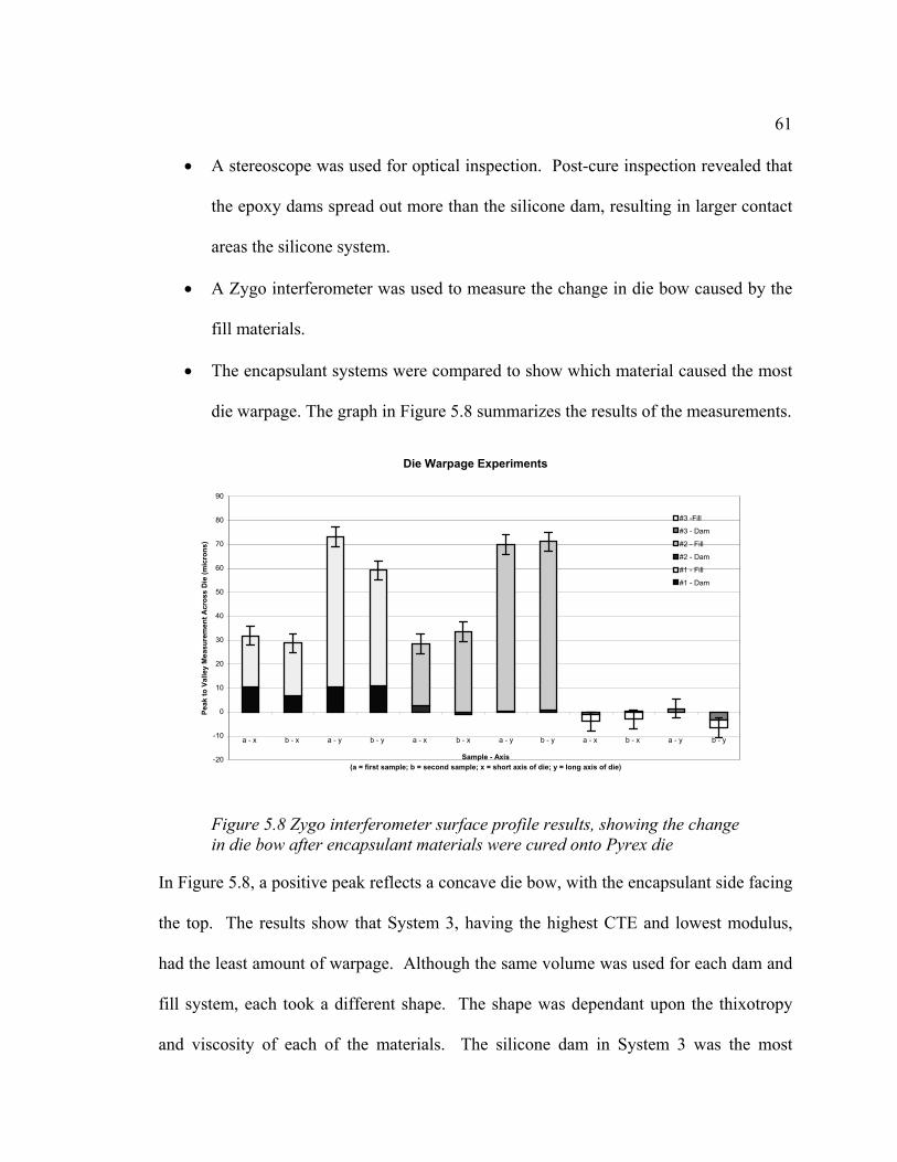


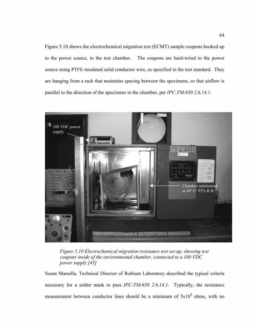


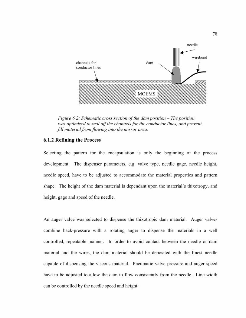

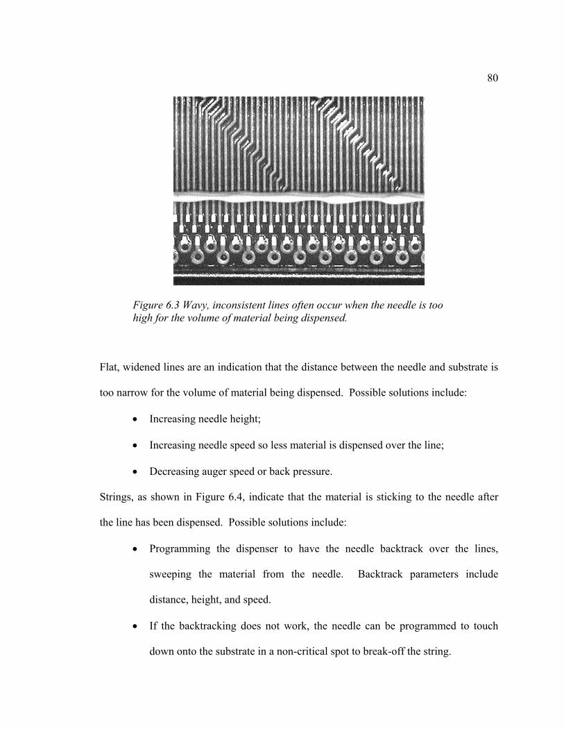


![Selective Opening Security from Simulatable Data Encapsulation · cently, security under receiver corruption gained some attention [20] while al- readydefinedin[1]. Work analysing](https://static.documents.pub/doc/80x56/5e7beedf3066dd18ec007516/selective-opening-security-from-simulatable-data-encapsulation-cently-security.jpg)


